US20030178120A1 - Working range setting method for bonding device for fabricating liquid crystal display devices - Google Patents
Working range setting method for bonding device for fabricating liquid crystal display devicesDownload PDFInfo
- Publication number
- US20030178120A1 US20030178120A1US10/259,698US25969802AUS2003178120A1US 20030178120 A1US20030178120 A1US 20030178120A1US 25969802 AUS25969802 AUS 25969802AUS 2003178120 A1US2003178120 A1US 2003178120A1
- Authority
- US
- United States
- Prior art keywords
- substrate
- working
- working range
- liquid crystal
- bonding device
- Prior art date
- Legal status (The legal status is an assumption and is not a legal conclusion. Google has not performed a legal analysis and makes no representation as to the accuracy of the status listed.)
- Granted
Links
Images


Classifications
- G—PHYSICS
- G02—OPTICS
- G02F—OPTICAL DEVICES OR ARRANGEMENTS FOR THE CONTROL OF LIGHT BY MODIFICATION OF THE OPTICAL PROPERTIES OF THE MEDIA OF THE ELEMENTS INVOLVED THEREIN; NON-LINEAR OPTICS; FREQUENCY-CHANGING OF LIGHT; OPTICAL LOGIC ELEMENTS; OPTICAL ANALOGUE/DIGITAL CONVERTERS
- G02F1/00—Devices or arrangements for the control of the intensity, colour, phase, polarisation or direction of light arriving from an independent light source, e.g. switching, gating or modulating; Non-linear optics
- G02F1/01—Devices or arrangements for the control of the intensity, colour, phase, polarisation or direction of light arriving from an independent light source, e.g. switching, gating or modulating; Non-linear optics for the control of the intensity, phase, polarisation or colour
- G02F1/13—Devices or arrangements for the control of the intensity, colour, phase, polarisation or direction of light arriving from an independent light source, e.g. switching, gating or modulating; Non-linear optics for the control of the intensity, phase, polarisation or colour based on liquid crystals, e.g. single liquid crystal display cells
- B—PERFORMING OPERATIONS; TRANSPORTING
- B32—LAYERED PRODUCTS
- B32B—LAYERED PRODUCTS, i.e. PRODUCTS BUILT-UP OF STRATA OF FLAT OR NON-FLAT, e.g. CELLULAR OR HONEYCOMB, FORM
- B32B38/00—Ancillary operations in connection with laminating processes
- B32B38/18—Handling of layers or the laminate
- B—PERFORMING OPERATIONS; TRANSPORTING
- B32—LAYERED PRODUCTS
- B32B—LAYERED PRODUCTS, i.e. PRODUCTS BUILT-UP OF STRATA OF FLAT OR NON-FLAT, e.g. CELLULAR OR HONEYCOMB, FORM
- B32B2309/00—Parameters for the laminating or treatment process; Apparatus details
- B32B2309/60—In a particular environment
- B32B2309/68—Vacuum
- B—PERFORMING OPERATIONS; TRANSPORTING
- B32—LAYERED PRODUCTS
- B32B—LAYERED PRODUCTS, i.e. PRODUCTS BUILT-UP OF STRATA OF FLAT OR NON-FLAT, e.g. CELLULAR OR HONEYCOMB, FORM
- B32B2457/00—Electrical equipment
- B32B2457/20—Displays, e.g. liquid crystal displays, plasma displays
- B—PERFORMING OPERATIONS; TRANSPORTING
- B32—LAYERED PRODUCTS
- B32B—LAYERED PRODUCTS, i.e. PRODUCTS BUILT-UP OF STRATA OF FLAT OR NON-FLAT, e.g. CELLULAR OR HONEYCOMB, FORM
- B32B2457/00—Electrical equipment
- B32B2457/20—Displays, e.g. liquid crystal displays, plasma displays
- B32B2457/202—LCD, i.e. liquid crystal displays
- Y—GENERAL TAGGING OF NEW TECHNOLOGICAL DEVELOPMENTS; GENERAL TAGGING OF CROSS-SECTIONAL TECHNOLOGIES SPANNING OVER SEVERAL SECTIONS OF THE IPC; TECHNICAL SUBJECTS COVERED BY FORMER USPC CROSS-REFERENCE ART COLLECTIONS [XRACs] AND DIGESTS
- Y10—TECHNICAL SUBJECTS COVERED BY FORMER USPC
- Y10S—TECHNICAL SUBJECTS COVERED BY FORMER USPC CROSS-REFERENCE ART COLLECTIONS [XRACs] AND DIGESTS
- Y10S414/00—Material or article handling
- Y10S414/135—Associated with semiconductor wafer handling
- Y10S414/136—Associated with semiconductor wafer handling including wafer orienting means
Definitions
- the present inventionrelates to a method for manufacturing a liquid crystal display (LCD) device, and more particularly, a working range setting method for a bonding device for manufacturing an LCD device.
- LCDliquid crystal display
- LCDliquid crystal display
- PDPplasma display panel
- ELDelectro-luminescent display
- VFDvacuum fluorescent display
- LCD devicesare commonly used because of their high resolution, light weight, thin profile, and low power consumption.
- LCD deviceshave been implemented in mobile devices, such as monitors for notebook computers, and have been developed for monitors of computers and televisions. Accordingly, efforts to improve image quality of LCD devices contrast with the benefits of their high resolution, light weight, thin profile, and low power consumption.
- image qualitysuch as fineness, brightness, large-sized area, for example, must be improved.
- LCD devicesare provided with an LCD panel for displaying image data and a driving unit for applying a driving signal to the LCD panel.
- the LCD panelis provided with first and second glass substrates bonded at a certain distance with liquid crystal material injected therebetween.
- a plurality of gate linesare formed along a first direction at fixed intervals on a first glass substrate (TFT array substrate), and a plurality of data lines are formed along a second direction perpendicular to the first direction, thereby defining a plurality of pixel regions.
- TFT array substratefirst glass substrate
- TFTthin film transistors
- black matrix filmsare commonly formed on a second glass substrate (color filter substrate) except at regions of the second glass substrate corresponding to the pixel regions of the first glass substrate. Also, a red, green, and blue color filter substrate is formed on the second glass substrate to generate colored light, and a common electrode is formed on the color filter substrate to produce images.
- Processes for manufacturing LCD devicesinclude injection and drop methods.
- the injection methodincludes steps of forming a sealant pattern on one of the first and second substrates to form an injection inlet, bonding the first and second substrates to each other within a vacuum processing chamber, and injecting liquid crystal material through the injection inlet.
- the drop method according to the related artwhich is disclosed in Japanese Patent Application Nos. 11-089612 and 11-172903, includes steps of dropping liquid crystal material on a first substrate, arranging a second substrate over the first substrate, and moving the first and second substrates to be adjacent to each other, thereby bonding the first and second substrates to each other.
- the injection methodrequired a considerably long process time since liquid crystal material is injected by osmotic pressure in a vacuum state. Accordingly, the injection method is inadequate for fabrication of large-sized LCD devices.
- the drop methodis a considerably shorter process time since the liquid crystal material is deposited on a first substrate and then bonded with a second substrate.
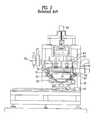
- FIG. 1is a cross sectional view of a bonding device for a liquid crystal display device according to the related art prior to a bonding process.
- a substrate bonding deviceincludes a frame 10 , an upper stage 21 , a lower stage 22 , a sealant dispenser (not shown), a liquid crystal material dispenser 30 , a processing chamber including an upper chamber unit 31 and a lower chamber unit 32 , a chamber moving system 40 , and a stage moving system 50 .
- the chamber moving system 40includes a driving motor driven to selectively move the lower chamber unit 32 to a location at which the bonding process is carried out, or to a location at which outflow of the sealant and dropping of the liquid crystal material occur.
- the stage moving system 50includes another driving motor driven to selectively move the upper stage 21 along a vertical direction perpendicular to the upper and lower stages 21 and 22 .
- a receiver-stopper systemtemporarily supports a substrate 52 , which is attached to the upper stage 21 , at both diagonal positions of the substrate 52 when an interior of the chamber is in a vacuum pressure state.
- the receiver-stopper systemincludes a rotation shaft 61 , a rotation actuator 63 , an elevation actuator 64 and support plates 62 for supporting corners of the substrate 52 .
- FIG. 2is a cross sectional view of a bonding device for a liquid crystal display device according to the related art during a bonding process
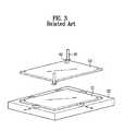
- FIG. 3is a perspective view of a substrate support system of a bonding device for a liquid crystal display device according to the related art.
- a second substrate 52is attached to the upper stage 21 , and a first substrate 51 is attached to the lower stage 22 .
- the lower chamber unit 32having the lower stage 22 , is moved by the chamber transfer means 40 to a working position for dispensing sealant and dropping liquid crystal material, as shown in FIG. 1.
- the lower chamber unit 32is moved again by the chamber transfer means 40 toward another working position for bonding between the substrates, as shown in FIG. 2 .
- the upper and lower chamber units 31 and 32are coupled together by the chamber transfer means 40 to enclose a space where the stages 21 and 22 are positioned, and the elevation actuator 64 and the rotation actuator 63 constituting the receiver-stopper system are actuated to place the support plates 62 under two corners of the second substrate, which is attached to the upper stage 31 . From this position, adsorptive force fixing the second substrate 52 is released to drop the second substrate 52 onto each of the support plates 62 of the receiver-stopper means as shown in FIG. 3.
- the bonding deviceincludes a number of working elements, specifically, working elements that require a considerable degree of precision, such as the stages and the substrate support means within the processing chamber. Accordingly, it is necessary to maintain the working elements at a precise distance according to the size and configuration of the first and second substrates. Moreover, since the first and second substrates may be different in their overall size and configuration and the substrates may have different cell configurations, it is necessary to carry out a selective operation according to the size and configuration of each substrate.
- each working elementpreferrably should be changed according to the size and configuration of each substrate. Moreover, it is necessary to prevent any damage in the cell area by the working elements supporting dummy areas rather than the cell area including the color filter or TFT arrays.
- the working elementmay need to be repositioned to a substrate having a second type of configuration different from the first configuration.
- the bonding devices according to the related artare disadvantageous since different configurations of substrates require changing the configuration of the working elements. Specifically, when bonding substrates have a configuration different from a previously processed set of substrates, the bonding device must be reconfigured to establish a new set of working ranges corresponding to the new bonded substrates. Accordingly, in order to perform the bonding process with a new configuration of substrates in the conventional bonding process the working range of the each working element must be reconfigured. Thus, a significant increase is production processing time is required.
- the present inventionis directed to a working range setting method of a working element for an LCD device that substantially obviates one or more problems due to limitations and disadvantages of the related art.
- An object of the present inventionis to provide a controlling method of a bonding device used in manufacturing an LCD device.
- a working range setting method of a bonding deviceincludes identifying a model of a first substrate, extracting a set value corresponding to a working range of working elements according to the identified model, and setting the working range of the corresponding working elements with the extracted set value.
- FIG. 1is a cross sectional view of a bonding device for a liquid crystal display device according to the related art prior to a bonding process
- FIG. 2is a cross sectional view of a bonding device for a liquid crystal display device according to the related art during a bonding process
- FIG. 3is a perspective view of a substrate support system of a bonding device for a liquid crystal display device according to the related art
- FIG. 4is a schematic view showing an exemplary arrangement of a bonding device for a liquid crystal display device according to the present invention
- FIG. 5is a flow chart showing an exemplary process of a bonding device for a liquid crystal display device according to the present invention
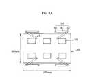
- FIG. 6Ais a plane view of an exemplary substrate support system for a bonding device according to the present invention.
- FIG. 6Bis a plane view of another exemplary substrate support system for a bonding device according to the present invention.
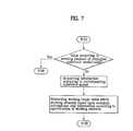
- FIG. 7is a flow chart showing an exemplary process of a bonding device for a liquid crystal display device according to the present invention.
- FIG. 4is a schematic view showing an exemplary arrangement of a bonding device for a liquid crystal display device according to the present invention.
- an arrangementmay include a substrate 100 , a controller 210 , a storage unit 220 , and a substrate reading unit 230 .
- the controller 210may control behaviors of various working elements of the bonding device and may collect various data from the storage unit 220 .
- the storage unit 220may set the working range of the working elements according to a configuration of each substrate 100 and may store set values for each of the working elements and substrates 100 .
- the substrate reading unit 230may identify a configuration of each substrate 100 that is transferred into the bonding device. For example, the substrate reading unit 230 may read out a code 110 positioned on the each substrate 100 to identify the specific configuration of the substrate 100 .
- FIG. 5is a flow chart showing an exemplary process of a bonding device for a liquid crystal display device according to the present invention
- FIG. 6Ais a plane view of an exemplary substrate support system for a bonding device according to the present invention
- FIG. 6Bis a plane view of another exemplary substrate support system for a bonding device according to the present invention.
- step S 110may include identifying a substrate configuration (i.e., model) using the substrate reading unit 230 (in FIG. 4) to read a code 110 (in FIG. 4) positioned on the substrate 100 (in FIG. 4).
- the code 110 (in FIG. 4)is stored in the controller 210 (in FIG. 4).
- step S 120if the code of the identified substrate 100 is identical to a code of the substrates that were used in a previous bonding process, the working elements are operated under the control of the controller to bond the corresponding substrates 100 without any change in the working range of the substrate support means 310 (in FIGS. 6A and 6B). However, if the code of the identified substrates 100 is different than a code of the substrates that were used in a previous bonding process, the controller 210 searches the storage unit 220 to extract a value set according to the working range of the substrate support means 310 with respect to the corresponding model.
- step S 130the controller 210 then re-sets the working range of the substrate support means 140 with the extracted value set.
- a rotation angle of the corresponding substrate support means 310is adjusted under the control of the controller 210 .
- the controller 210After resetting of the rotation angle of the substrate support means 310 with respect to the corresponding substrate model is completed, the controller 210 performs a control adjustment of the set values, so that the substrate support means 310 rotates at a rotation angle ⁇ different than a previous angle ⁇ to support the corresponding substrate 100 .
- FIG. 7is a flow chart showing an exemplary process of a bonding device for a liquid crystal display device according to the present invention.
- a new set of corresponding working ranges of the substrate support means 310 based upon various information according to the model of the corresponding substrate 100is produced. Then, this new working range is stored in the storage unit 220 , and is re-set as the working range of the substrate support means.
- the working range of the substrate support means 310for a new model of substrate, can be manually entered by an operator, it is also proposed that the rotation angle of the substrate support means 310 can be automatically set based upon the number and position of the cells 120 formed in the corresponding substrate 100 and values entered with respect to the position of dummy area formed in the corresponding substrate 100 . In particular, this may be done by extracting the rotation angle or the working range of the substrate support means 310 by using a virtual working simulation program.
- the virtual working simulation programis established to simulate and display the working position based upon the specification (i.e., length, height, and thickness) of each working element that was previously registered.
- Various informationis entered according to the model of the each substrate 100 , and may be provided in the form of a Computer Aided Design (CAD) program.
- CADComputer Aided Design
- the programuses information, such as the length of support parts 311 of the substrate support means 310 , the position of support projections 312 formed in the support parts 311 , and the position of rotation shafts 313 for rotating the support parts 311 to simulate the position of the support projections 312 that is varied as the support parts 311 are varied in angle.
- the programcan extract the position where the support projections 312 can stably support the corresponding substrate 100 without droop.
- a plurality of the support projections 312may be provided to enable correspondence with respect to the model of each substrate or varied in position according to the model of each substrate.
- the value extractedmay be entered into the storage unit 220 as the working range of the substrate support means 310 , which is sorted according to the model of the corresponding substrate 100 , so that control can be executed based upon the set value in the above entered working range when the corresponding model of substrate is transferred later.
- each working element presented in the inventionis not necessarily restricted to the substrate support means 310 , but may include various other elements such as the upper and lower stages for loading a pair of substrates to execute a bonding process between the substrates, auxiliary loading means for loading a substrate onto the lower stage when the substrate is transferred to be loaded onto the lower stage, alignment means for aligning the position between substrates loaded onto the stages, clamping means for loading or fixing the substrates which are respectively fixed to the stages, and auxiliary process means for assisting various procedures for bonding between the substrates.
Landscapes
- Physics & Mathematics (AREA)
- Nonlinear Science (AREA)
- Liquid Crystal (AREA)
- Chemical & Material Sciences (AREA)
- Crystallography & Structural Chemistry (AREA)
- General Physics & Mathematics (AREA)
- Optics & Photonics (AREA)
Abstract
Description
- The present invention claims the benefit of Korean Patent Application No. P2002-15960 filed in Korea on Mar. 25, 2002, which is hereby incorporated by reference.[0001]
- 1. Field of the Invention[0002]
- The present invention relates to a method for manufacturing a liquid crystal display (LCD) device, and more particularly, a working range setting method for a bonding device for manufacturing an LCD device.[0003]
- 2. Discussion of the Related Art[0004]
- In response to an increasing demand for various types of display devices, liquid crystal display (LCD), plasma display panel (PDP), electro-luminescent display (ELD), and vacuum fluorescent display (VFD) have been developed. In particular, LCD devices are commonly used because of their high resolution, light weight, thin profile, and low power consumption. In addition, LCD devices have been implemented in mobile devices, such as monitors for notebook computers, and have been developed for monitors of computers and televisions. Accordingly, efforts to improve image quality of LCD devices contrast with the benefits of their high resolution, light weight, thin profile, and low power consumption. In order to incorporate LCD devices as a general image display, image quality such as fineness, brightness, large-sized area, for example, must be improved.[0005]
- LCD devices are provided with an LCD panel for displaying image data and a driving unit for applying a driving signal to the LCD panel. The LCD panel is provided with first and second glass substrates bonded at a certain distance with liquid crystal material injected therebetween. A plurality of gate lines are formed along a first direction at fixed intervals on a first glass substrate (TFT array substrate), and a plurality of data lines are formed along a second direction perpendicular to the first direction, thereby defining a plurality of pixel regions. Then, a plurality of pixel electrodes are formed in a matrix arrangement at the pixel regions, and a plurality of thin film transistors (TFT) are formed at the pixel regions. Accordingly, the plurality of thin film transistors are enabled by signals transmitted along the gate lines and transfer signals transmitted along the data lines to each pixel electrode.[0006]
- In order to prevent light leakage, black matrix films are commonly formed on a second glass substrate (color filter substrate) except at regions of the second glass substrate corresponding to the pixel regions of the first glass substrate. Also, a red, green, and blue color filter substrate is formed on the second glass substrate to generate colored light, and a common electrode is formed on the color filter substrate to produce images.[0007]
- Processes for manufacturing LCD devices include injection and drop methods. The injection method, according to the related art, includes steps of forming a sealant pattern on one of the first and second substrates to form an injection inlet, bonding the first and second substrates to each other within a vacuum processing chamber, and injecting liquid crystal material through the injection inlet. The drop method according to the related art, which is disclosed in Japanese Patent Application Nos. 11-089612 and 11-172903, includes steps of dropping liquid crystal material on a first substrate, arranging a second substrate over the first substrate, and moving the first and second substrates to be adjacent to each other, thereby bonding the first and second substrates to each other.[0008]
- However, the injection method required a considerably long process time since liquid crystal material is injected by osmotic pressure in a vacuum state. Accordingly, the injection method is inadequate for fabrication of large-sized LCD devices. On the other hand, the drop method is a considerably shorter process time since the liquid crystal material is deposited on a first substrate and then bonded with a second substrate.[0009]
- FIG. 1 is a cross sectional view of a bonding device for a liquid crystal display device according to the related art prior to a bonding process. In FIG. 1, a substrate bonding device includes a[0010]
frame 10, anupper stage 21, alower stage 22, a sealant dispenser (not shown), a liquidcrystal material dispenser 30, a processing chamber including anupper chamber unit 31 and alower chamber unit 32, achamber moving system 40, and astage moving system 50. Thechamber moving system 40 includes a driving motor driven to selectively move thelower chamber unit 32 to a location at which the bonding process is carried out, or to a location at which outflow of the sealant and dropping of the liquid crystal material occur. Thestage moving system 50 includes another driving motor driven to selectively move theupper stage 21 along a vertical direction perpendicular to the upper andlower stages - A receiver-stopper system temporarily supports a[0011]
substrate 52, which is attached to theupper stage 21, at both diagonal positions of thesubstrate 52 when an interior of the chamber is in a vacuum pressure state. At this time, the receiver-stopper system includes arotation shaft 61, arotation actuator 63, anelevation actuator 64 andsupport plates 62 for supporting corners of thesubstrate 52. - A process of manufacturing a liquid crystal display device using the substrate assembly device according to the prior art will be described with reference to FIG. 2, which is a cross sectional view of a bonding device for a liquid crystal display device according to the related art during a bonding process, and FIG. 3 is a perspective view of a substrate support system of a bonding device for a liquid crystal display device according to the related art.[0012]
- First, a[0013]
second substrate 52 is attached to theupper stage 21, and afirst substrate 51 is attached to thelower stage 22. Then, thelower chamber unit 32, having thelower stage 22, is moved by the chamber transfer means40 to a working position for dispensing sealant and dropping liquid crystal material, as shown in FIG. 1. After the sealant dispensing process and the liquid crystal material dropping process are completed on thefirst substrate 51, thelower chamber unit 32 is moved again by the chamber transfer means40 toward another working position for bonding between the substrates, as shown in FIG.2. Then, the upper andlower chamber units stages elevation actuator 64 and therotation actuator 63 constituting the receiver-stopper system are actuated to place thesupport plates 62 under two corners of the second substrate, which is attached to theupper stage 31. From this position, adsorptive force fixing thesecond substrate 52 is released to drop thesecond substrate 52 onto each of thesupport plates 62 of the receiver-stopper means as shown in FIG. 3. - At this time, pressure in an interior of the processing chamber is reduced to produce a vacuum state by a vacuum system. When the interior of the processing chamber is evacuated, an electrostatic force is applied to the[0014]
upper stage 31 to attach thesecond substrate 52 while therotation actuator 63 and theelevation actuator 64 are actuated so that thesupport plates 62 and therotation shaft 61 do not obstruct bonding of the substrates. In the vacuum state, theupper stage 21 is moved downward by the stage transfer means50, and bonds thesecond substrate 52, which is attached to theupper stage 21, and thefirst substrate 51, which is fixedly settled on the lower stage, thereby completing manufacturing processes of an LCD device. - The bonding device according the related art includes a number of working elements, specifically, working elements that require a considerable degree of precision, such as the stages and the substrate support means within the processing chamber. Accordingly, it is necessary to maintain the working elements at a precise distance according to the size and configuration of the first and second substrates. Moreover, since the first and second substrates may be different in their overall size and configuration and the substrates may have different cell configurations, it is necessary to carry out a selective operation according to the size and configuration of each substrate.[0015]
- Considering that overall size of substrates are gradually increasing, there is a need to prevent drooping of the substrate by supporting an inside of the substrate rather than by supporting the corners during bonding processes. Accordingly, the working position of each working element preferrably should be changed according to the size and configuration of each substrate. Moreover, it is necessary to prevent any damage in the cell area by the working elements supporting dummy areas rather than the cell area including the color filter or TFT arrays.[0016]
- However, as overall size and configuration of the substrates changes, positions and overall size of the cell area on the substrate is altered. Thus, once the working element is reproducibly positioned for a substrate having a first type of configuration, the working element may need to be repositioned to a substrate having a second type of configuration different from the first configuration. The bonding devices according to the related art are disadvantageous since different configurations of substrates require changing the configuration of the working elements. Specifically, when bonding substrates have a configuration different from a previously processed set of substrates, the bonding device must be reconfigured to establish a new set of working ranges corresponding to the new bonded substrates. Accordingly, in order to perform the bonding process with a new configuration of substrates in the conventional bonding process the working range of the each working element must be reconfigured. Thus, a significant increase is production processing time is required.[0017]
- Accordingly, the present invention is directed to a working range setting method of a working element for an LCD device that substantially obviates one or more problems due to limitations and disadvantages of the related art.[0018]
- An object of the present invention is to provide a controlling method of a bonding device used in manufacturing an LCD device.[0019]
- Additional features and advantages of the invention will be set forth in the description which follows, and in part will become apparent from the description, or may be learned from practice of the invention. The objectives and other advantages of the invention will be realized and attained by the structure particularly pointed out in the written description and claims hereof as well as the appended drawings.[0020]
- To achieve these objects and other advantages and in accordance with the purpose of the invention, as embodied and broadly described herein, a working range setting method of a bonding device includes identifying a model of a first substrate, extracting a set value corresponding to a working range of working elements according to the identified model, and setting the working range of the corresponding working elements with the extracted set value.[0021]
- It is to be understood that both the foregoing general description and the following detailed description of the present invention are exemplary and explanatory and are intended to provide further explanation of the invention as claimed.[0022]
- The accompanying drawings, which are included to provide a further understanding of the invention and are incorporated in and constitute a part of this application, illustrate embodiments of the invention and together with the description serve to explain the principle of the invention. In the drawings:[0023]
- FIG. 1 is a cross sectional view of a bonding device for a liquid crystal display device according to the related art prior to a bonding process;[0024]
- FIG. 2 is a cross sectional view of a bonding device for a liquid crystal display device according to the related art during a bonding process;[0025]
- FIG. 3 is a perspective view of a substrate support system of a bonding device for a liquid crystal display device according to the related art;[0026]
- FIG. 4 is a schematic view showing an exemplary arrangement of a bonding device for a liquid crystal display device according to the present invention;[0027]
- FIG. 5 is a flow chart showing an exemplary process of a bonding device for a liquid crystal display device according to the present invention;[0028]
- FIG. 6A is a plane view of an exemplary substrate support system for a bonding device according to the present invention;[0029]
- FIG. 6B is a plane view of another exemplary substrate support system for a bonding device according to the present invention; and[0030]
- FIG. 7 is a flow chart showing an exemplary process of a bonding device for a liquid crystal display device according to the present invention.[0031]
- Reference will now be made in detail to the preferred embodiments of the present invention, examples of which are illustrated in the accompanying drawings.[0032]
- FIG. 4 is a schematic view showing an exemplary arrangement of a bonding device for a liquid crystal display device according to the present invention. In FIG. 4, an arrangement may include a[0033]
substrate 100, acontroller 210, astorage unit 220, and asubstrate reading unit 230. Thecontroller 210 may control behaviors of various working elements of the bonding device and may collect various data from thestorage unit 220. Thestorage unit 220 may set the working range of the working elements according to a configuration of eachsubstrate 100 and may store set values for each of the working elements andsubstrates 100. Thesubstrate reading unit 230 may identify a configuration of eachsubstrate 100 that is transferred into the bonding device. For example, thesubstrate reading unit 230 may read out acode 110 positioned on the eachsubstrate 100 to identify the specific configuration of thesubstrate 100. - FIG. 5 is a flow chart showing an exemplary process of a bonding device for a liquid crystal display device according to the present invention, FIG. 6A is a plane view of an exemplary substrate support system for a bonding device according to the present invention, and FIG. 6B is a plane view of another exemplary substrate support system for a bonding device according to the present invention. In FIG. 5, step S[0034]110 may include identifying a substrate configuration (i.e., model) using the substrate reading unit230 (in FIG. 4) to read a code110 (in FIG. 4) positioned on the substrate100 (in FIG. 4). The code110 (in FIG. 4) is stored in the controller210 (in FIG. 4).
- At step S[0035]120, if the code of the identified
substrate 100 is identical to a code of the substrates that were used in a previous bonding process, the working elements are operated under the control of the controller to bond the correspondingsubstrates 100 without any change in the working range of the substrate support means310 (in FIGS. 6A and 6B). However, if the code of the identifiedsubstrates 100 is different than a code of the substrates that were used in a previous bonding process, thecontroller 210 searches thestorage unit 220 to extract a value set according to the working range of the substrate support means310 with respect to the corresponding model. - At step S[0036]130, the
controller 210 then re-sets the working range of the substrate support means140 with the extracted value set. - For example, in a case where substrates each have twelve cells[0037]120 (i.e. a model different from the previous one), are transferred as shown in FIG. 6B in a state that the substrate support means310 is pre-set at a rotation angle to support
substrates 100 each having sixcells 120 and a size of 1000×1200 mm as shown in FIG. 6A, a rotation angle of the corresponding substrate support means310 is adjusted under the control of thecontroller 210. - After resetting of the rotation angle of the substrate support means[0038]310 with respect to the corresponding substrate model is completed, the
controller 210 performs a control adjustment of the set values, so that the substrate support means310 rotates at a rotation angle α different than a previous angle θ to support the correspondingsubstrate 100. - FIG. 7 is a flow chart showing an exemplary process of a bonding device for a liquid crystal display device according to the present invention. In FIG. 7, when the set value for the working range of the working element is not registered in the[0039]
storage unit 220 corresponding to the model of thesubstrate 100 carried in for the bonding process, a new set of corresponding working ranges of the substrate support means310 based upon various information according to the model of thecorresponding substrate 100 is produced. Then, this new working range is stored in thestorage unit 220, and is re-set as the working range of the substrate support means. - Although the working range of the substrate support means[0040]310, for a new model of substrate, can be manually entered by an operator, it is also proposed that the rotation angle of the substrate support means310 can be automatically set based upon the number and position of the
cells 120 formed in thecorresponding substrate 100 and values entered with respect to the position of dummy area formed in thecorresponding substrate 100. In particular, this may be done by extracting the rotation angle or the working range of the substrate support means310 by using a virtual working simulation program. - The virtual working simulation program is established to simulate and display the working position based upon the specification (i.e., length, height, and thickness) of each working element that was previously registered. Various information is entered according to the model of the each[0041]
substrate 100, and may be provided in the form of a Computer Aided Design (CAD) program. Accordingly, when the entire size of thecorresponding substrate 100 and the number and position of thecells 120 are entered into the working simulation program, the program uses information, such as the length ofsupport parts 311 of the substrate support means310, the position ofsupport projections 312 formed in thesupport parts 311, and the position ofrotation shafts 313 for rotating thesupport parts 311 to simulate the position of thesupport projections 312 that is varied as thesupport parts 311 are varied in angle. In this manner, the program can extract the position where thesupport projections 312 can stably support the correspondingsubstrate 100 without droop. In addition, a plurality of thesupport projections 312 may be provided to enable correspondence with respect to the model of each substrate or varied in position according to the model of each substrate. - The value extracted may be entered into the[0042]
storage unit 220 as the working range of the substrate support means310, which is sorted according to the model of thecorresponding substrate 100, so that control can be executed based upon the set value in the above entered working range when the corresponding model of substrate is transferred later. Moreover, each working element presented in the invention is not necessarily restricted to the substrate support means310, but may include various other elements such as the upper and lower stages for loading a pair of substrates to execute a bonding process between the substrates, auxiliary loading means for loading a substrate onto the lower stage when the substrate is transferred to be loaded onto the lower stage, alignment means for aligning the position between substrates loaded onto the stages, clamping means for loading or fixing the substrates which are respectively fixed to the stages, and auxiliary process means for assisting various procedures for bonding between the substrates. - It will be apparent to those skilled in the art that various modifications and variations can be made in the working range setting method for a bonding device for fabricating liquid crystal display devices of the present invention. Thus, it is intended that the present invention covers the modifications and variations of this invention provided they come within the scope of the appended claims and their equivalents.[0043]
Claims (10)
Applications Claiming Priority (2)
| Application Number | Priority Date | Filing Date | Title |
|---|---|---|---|
| KRP2002-15960 | 2002-03-25 | ||
| KR1020020015960AKR100720420B1 (en) | 2002-03-25 | 2002-03-25 | Operation control method of bonding apparatus for liquid crystal display device and apparatus therefor |
Publications (2)
| Publication Number | Publication Date |
|---|---|
| US20030178120A1true US20030178120A1 (en) | 2003-09-25 |
| US7214283B2 US7214283B2 (en) | 2007-05-08 |
Family
ID=28036175
Family Applications (1)
| Application Number | Title | Priority Date | Filing Date |
|---|---|---|---|
| US10/259,698Expired - LifetimeUS7214283B2 (en) | 2002-03-25 | 2002-09-30 | Working range setting method for bonding device for fabricating liquid crystal display devices |
Country Status (2)
| Country | Link |
|---|---|
| US (1) | US7214283B2 (en) |
| KR (1) | KR100720420B1 (en) |
Cited By (1)
| Publication number | Priority date | Publication date | Assignee | Title |
|---|---|---|---|---|
| US20060287960A1 (en)* | 2005-06-21 | 2006-12-21 | International Business Machines Corporation | System, method and program product to identify unutilized or underutilized software license |
Citations (39)
| Publication number | Priority date | Publication date | Assignee | Title |
|---|---|---|---|---|
| US3978580A (en)* | 1973-06-28 | 1976-09-07 | Hughes Aircraft Company | Method of fabricating a liquid crystal display |
| US4094058A (en)* | 1976-07-23 | 1978-06-13 | Omron Tateisi Electronics Co. | Method of manufacture of liquid crystal displays |
| US4653864A (en)* | 1986-02-26 | 1987-03-31 | Ovonic Imaging Systems, Inc. | Liquid crystal matrix display having improved spacers and method of making same |
| US4691995A (en)* | 1985-07-15 | 1987-09-08 | Semiconductor Energy Laboratory Co., Ltd. | Liquid crystal filling device |
| US4696712A (en)* | 1983-11-07 | 1987-09-29 | Disco Abrasive Systems, Ltd. | Semiconductor wafer mounting and cutting system |
| US4775225A (en)* | 1985-05-16 | 1988-10-04 | Canon Kabushiki Kaisha | Liquid crystal device having pillar spacers with small base periphery width in direction perpendicular to orientation treatment |
| US5247377A (en)* | 1988-07-23 | 1993-09-21 | Rohm Gmbh Chemische Fabrik | Process for producing anisotropic liquid crystal layers on a substrate |
| US5263888A (en)* | 1992-02-20 | 1993-11-23 | Matsushita Electric Industrial Co., Ltd. | Method of manufacture of liquid crystal display panel |
| US5379139A (en)* | 1986-08-20 | 1995-01-03 | Semiconductor Energy Laboratory Co., Ltd. | Liquid crystal device and method for manufacturing same with spacers formed by photolithography |
| US5406989A (en)* | 1993-10-12 | 1995-04-18 | Ayumi Industry Co., Ltd. | Method and dispenser for filling liquid crystal into LCD cell |
| US5499128A (en)* | 1993-03-15 | 1996-03-12 | Kabushiki Kaisha Toshiba | Liquid crystal display device with acrylic polymer spacers and method of manufacturing the same |
| US5507323A (en)* | 1993-10-12 | 1996-04-16 | Fujitsu Limited | Method and dispenser for filling liquid crystal into LCD cell |
| US5539545A (en)* | 1993-05-18 | 1996-07-23 | Semiconductor Energy Laboratory Co., Ltd. | Method of making LCD in which resin columns are cured and the liquid crystal is reoriented |
| US5548429A (en)* | 1993-06-14 | 1996-08-20 | Canon Kabushiki Kaisha | Process for producing liquid crystal device whereby curing the sealant takes place after pre-baking the substrates |
| US5642214A (en)* | 1991-07-19 | 1997-06-24 | Sharp Kabushiki Kaisha | Optical modulating element and electronic apparatus using it |
| US5742370A (en)* | 1996-09-12 | 1998-04-21 | Korea Institute Of Science And Technology | Fabrication method for liquid crystal alignment layer by magnetic field treatment |
| US5757451A (en)* | 1995-09-08 | 1998-05-26 | Kabushiki Kaisha Toshiba | Liquid crystal display device spacers formed from stacked color layers |
| US5852484A (en)* | 1994-09-26 | 1998-12-22 | Matsushita Electric Industrial Co., Ltd. | Liquid crystal display panel and method and device for manufacturing the same |
| US5861932A (en)* | 1997-03-31 | 1999-01-19 | Denso Corporation | Liquid crystal cell and its manufacturing method |
| US5875922A (en)* | 1997-10-10 | 1999-03-02 | Nordson Corporation | Apparatus for dispensing an adhesive |
| US5882451A (en)* | 1996-03-27 | 1999-03-16 | Matsushita Electric Industrial Co., Ltd. | Method and apparatus for applying an electronic component adhesive |
| US5952676A (en)* | 1986-08-20 | 1999-09-14 | Semiconductor Energy Laboratory Co., Ltd. | Liquid crystal device and method for manufacturing same with spacers formed by photolithography |
| US5956112A (en)* | 1995-10-02 | 1999-09-21 | Sharp Kabushiki Kaisha | Liquid crystal display device and method for manufacturing the same |
| US6001203A (en)* | 1995-03-01 | 1999-12-14 | Matsushita Electric Industrial Co., Ltd. | Production process of liquid crystal display panel, seal material for liquid crystal cell and liquid crystal display |
| US6011609A (en)* | 1996-10-05 | 2000-01-04 | Samsung Electronics Co., Ltd. | Method of manufacturing LCD by dropping liquid crystals on a substrate and then pressing the substrates |
| US6016178A (en)* | 1996-09-13 | 2000-01-18 | Sony Corporation | Reflective guest-host liquid-crystal display device |
| US6016181A (en)* | 1996-11-07 | 2000-01-18 | Sharp Kabushiki Kaisha | Liquid crystal device having column spacers with portion on each of the spacers for reflecting or absorbing visible light and method for fabricating the same |
| US6055035A (en)* | 1998-05-11 | 2000-04-25 | International Business Machines Corporation | Method and apparatus for filling liquid crystal display (LCD) panels |
| US6163357A (en)* | 1996-09-26 | 2000-12-19 | Kabushiki Kaisha Toshiba | Liquid crystal display device having the driving circuit disposed in the seal area, with different spacer density in driving circuit area than display area |
| US6219126B1 (en)* | 1998-11-20 | 2001-04-17 | International Business Machines Corporation | Panel assembly for liquid crystal displays having a barrier fillet and an adhesive fillet in the periphery |
| US6226067B1 (en)* | 1997-10-03 | 2001-05-01 | Minolta Co., Ltd. | Liquid crystal device having spacers and manufacturing method thereof |
| US6236445B1 (en)* | 1996-02-22 | 2001-05-22 | Hughes Electronics Corporation | Method for making topographic projections |
| US20010021000A1 (en)* | 2000-02-02 | 2001-09-13 | Norihiko Egami | Apparatus and method for manufacturing liquid crystal display |
| US6304311B1 (en)* | 1998-11-16 | 2001-10-16 | Matsushita Electric Industrial Co., Ltd. | Method of manufacturing liquid crystal display device |
| US6304306B1 (en)* | 1995-02-17 | 2001-10-16 | Sharp Kabushiki Kaisha | Liquid crystal display device and method for producing the same |
| US6337730B1 (en)* | 1998-06-02 | 2002-01-08 | Denso Corporation | Non-uniformly-rigid barrier wall spacers used to correct problems caused by thermal contraction of smectic liquid crystal material |
| US20020047983A1 (en)* | 2000-08-31 | 2002-04-25 | Hannstar Display Corp. | Apparatus and method for pressing and combining two substrates of a LCD panel |
| US6414733B1 (en)* | 1999-02-08 | 2002-07-02 | Dai Nippon Printing Co., Ltd. | Color liquid crystal display with a shielding member being arranged between sealing member and display zone |
| US20020117267A1 (en)* | 2001-02-01 | 2002-08-29 | Shibaura Mechatronics Corporation | Electric component compression bonding machine and method |
Family Cites Families (129)
| Publication number | Priority date | Publication date | Assignee | Title |
|---|---|---|---|---|
| JPS5165656A (en) | 1974-12-04 | 1976-06-07 | Shinshu Seiki Kk | |
| JPS52149725A (en) | 1976-06-07 | 1977-12-13 | Ichikoh Ind Ltd | Non contact system lamp checker for vehicle |
| JPS5738414A (en) | 1980-08-20 | 1982-03-03 | Showa Denko Kk | Spacer for display panel |
| JPS5788428A (en) | 1980-11-20 | 1982-06-02 | Ricoh Elemex Corp | Manufacture of liquid crystal display body device |
| JPS5827126A (en) | 1981-08-11 | 1983-02-17 | Nec Corp | Production of liquid crystal display panel |
| JPS5957221A (en) | 1982-09-28 | 1984-04-02 | Asahi Glass Co Ltd | Production of display element |
| JPS59195222A (en) | 1983-04-19 | 1984-11-06 | Matsushita Electric Ind Co Ltd | Manufacture of liquid-crystal panel |
| JPS60111221A (en) | 1983-11-19 | 1985-06-17 | Nippon Denso Co Ltd | Method and device for charging liquid crystal |
| JPS60164723A (en) | 1984-02-07 | 1985-08-27 | Seiko Instr & Electronics Ltd | Liquid crystal display device |
| JPS60217343A (en) | 1984-04-13 | 1985-10-30 | Matsushita Electric Ind Co Ltd | Liquid crystal display device and its preparation |
| JPS617822A (en) | 1984-06-22 | 1986-01-14 | Canon Inc | Production of liquid crystal element |
| JPS6155625A (en) | 1984-08-24 | 1986-03-20 | Nippon Denso Co Ltd | Manufacture of liquid crystal element |
| JPS6289025A (en) | 1985-10-15 | 1987-04-23 | Matsushita Electric Ind Co Ltd | Manufacturing method of liquid crystal display panel |
| JPS6290622A (en) | 1985-10-17 | 1987-04-25 | Seiko Epson Corp | liquid crystal display device |
| JPH0668589B2 (en) | 1986-03-06 | 1994-08-31 | キヤノン株式会社 | Ferroelectric liquid crystal element |
| JPS63109413A (en) | 1986-10-27 | 1988-05-14 | Fujitsu Ltd | Manufacturing method of LCD display |
| JPS63110425A (en) | 1986-10-29 | 1988-05-14 | Toppan Printing Co Ltd | Cell for liquid crystal filling |
| JPS63128315A (en) | 1986-11-19 | 1988-05-31 | Victor Co Of Japan Ltd | Liquid crystal display element |
| JPS63311233A (en) | 1987-06-12 | 1988-12-20 | Toyota Motor Corp | lcd cell |
| JPH05127179A (en) | 1991-11-01 | 1993-05-25 | Ricoh Co Ltd | Production of liquid crystal display element |
| JP2609386B2 (en) | 1991-12-06 | 1997-05-14 | 株式会社日立製作所 | Board assembly equipment |
| JPH05265011A (en) | 1992-03-19 | 1993-10-15 | Seiko Instr Inc | Production of liquid crystal display element |
| JP2939384B2 (en) | 1992-04-01 | 1999-08-25 | 松下電器産業株式会社 | Liquid crystal panel manufacturing method |
| JPH05281562A (en) | 1992-04-01 | 1993-10-29 | Matsushita Electric Ind Co Ltd | Manufacture of liquid crystal panel |
| JPH0651256A (en) | 1992-07-30 | 1994-02-25 | Matsushita Electric Ind Co Ltd | Device for discharging liquid crystal |
| JP3084975B2 (en) | 1992-11-06 | 2000-09-04 | 松下電器産業株式会社 | Liquid crystal display cell manufacturing equipment |
| JPH06160871A (en) | 1992-11-26 | 1994-06-07 | Matsushita Electric Ind Co Ltd | Liquid crystal display panel and manufacturing method thereof |
| JPH06235925A (en) | 1993-02-10 | 1994-08-23 | Matsushita Electric Ind Co Ltd | Manufacture of liquid crystal display element |
| JPH06265915A (en) | 1993-03-12 | 1994-09-22 | Matsushita Electric Ind Co Ltd | Discharge device for filling liquid crystal |
| JP3170773B2 (en) | 1993-04-28 | 2001-05-28 | 株式会社日立製作所 | Board assembly equipment |
| JP3260511B2 (en) | 1993-09-13 | 2002-02-25 | 株式会社日立製作所 | Sealant drawing method |
| JPH07128674A (en) | 1993-11-05 | 1995-05-19 | Matsushita Electric Ind Co Ltd | Liquid crystal display element manufacturing method |
| JPH07181507A (en) | 1993-12-21 | 1995-07-21 | Canon Inc | Liquid crystal display device and information transmission device including the liquid crystal display device |
| JPH086910A (en)* | 1994-06-23 | 1996-01-12 | Hitachi Ltd | Cluster computer system |
| JP3189591B2 (en) | 1994-09-27 | 2001-07-16 | 松下電器産業株式会社 | Manufacturing method of liquid crystal element |
| JPH08101395A (en) | 1994-09-30 | 1996-04-16 | Matsushita Electric Ind Co Ltd | Liquid crystal display element manufacturing method |
| JPH08106101A (en) | 1994-10-06 | 1996-04-23 | Fujitsu Ltd | Liquid crystal display panel manufacturing method |
| JPH08171094A (en) | 1994-12-19 | 1996-07-02 | Nippon Soken Inc | Liquid crystal injecting method and liquid crystal injecting device to liquid crystal display device |
| JP3545076B2 (en) | 1995-01-11 | 2004-07-21 | 富士通ディスプレイテクノロジーズ株式会社 | Liquid crystal display device and method of manufacturing the same |
| JP3534474B2 (en) | 1995-03-06 | 2004-06-07 | 富士通ディスプレイテクノロジーズ株式会社 | Liquid crystal display panel sealing method |
| JPH095762A (en) | 1995-06-20 | 1997-01-10 | Matsushita Electric Ind Co Ltd | Liquid crystal panel manufacturing method |
| JP3978241B2 (en) | 1995-07-10 | 2007-09-19 | シャープ株式会社 | Liquid crystal display panel and manufacturing method thereof |
| JPH0961829A (en) | 1995-08-21 | 1997-03-07 | Matsushita Electric Ind Co Ltd | Liquid crystal display element manufacturing method |
| JPH0973075A (en) | 1995-09-05 | 1997-03-18 | Matsushita Electric Ind Co Ltd | Liquid crystal display element manufacturing method and liquid crystal display element manufacturing apparatus |
| JP3161296B2 (en) | 1995-09-05 | 2001-04-25 | 松下電器産業株式会社 | Manufacturing method of liquid crystal display element |
| JP3658604B2 (en) | 1995-10-27 | 2005-06-08 | 富士通ディスプレイテクノロジーズ株式会社 | Manufacturing method of liquid crystal panel |
| JPH09197423A (en)* | 1996-01-18 | 1997-07-31 | Toshiba Corp | Coating device |
| JPH09230357A (en) | 1996-02-22 | 1997-09-05 | Canon Inc | Liquid crystal panel manufacturing method and liquid crystal cell used therefor |
| JP3790295B2 (en) | 1996-04-17 | 2006-06-28 | シャープ株式会社 | Manufacturing method of liquid crystal display panel |
| JP3234496B2 (en) | 1996-05-21 | 2001-12-04 | 松下電器産業株式会社 | Manufacturing method of liquid crystal display device |
| JPH10123537A (en) | 1996-10-15 | 1998-05-15 | Matsushita Electric Ind Co Ltd | Liquid crystal display device and method of manufacturing the same |
| JP3088960B2 (en) | 1996-10-22 | 2000-09-18 | 松下電器産業株式会社 | Manufacturing method of liquid crystal display element |
| JPH10142616A (en) | 1996-11-14 | 1998-05-29 | Ayumi Kogyo Kk | Liquid crystal injection method and liquid dispenser |
| JPH10177178A (en) | 1996-12-17 | 1998-06-30 | Matsushita Electric Ind Co Ltd | Manufacturing method of liquid crystal display element |
| JP3874871B2 (en) | 1997-02-10 | 2007-01-31 | シャープ株式会社 | Manufacturing method of liquid crystal display device |
| JP3773326B2 (en) | 1997-04-07 | 2006-05-10 | アユミ工業株式会社 | Liquid crystal injection method and dispenser used therefor |
| JPH10333157A (en) | 1997-06-03 | 1998-12-18 | Matsushita Electric Ind Co Ltd | Manufacturing method of liquid crystal display device |
| JPH10333159A (en) | 1997-06-03 | 1998-12-18 | Matsushita Electric Ind Co Ltd | Liquid crystal display |
| JPH1114953A (en) | 1997-06-20 | 1999-01-22 | Matsushita Electric Ind Co Ltd | Method of manufacturing multi-touch liquid crystal display panel and multi-touch liquid crystal display panel |
| JP3874895B2 (en) | 1997-07-23 | 2007-01-31 | シャープ株式会社 | Manufacturing method of liquid crystal display panel |
| JPH1164811A (en) | 1997-08-21 | 1999-03-05 | Matsushita Electric Ind Co Ltd | Method and apparatus for manufacturing liquid crystal display element |
| JPH11109388A (en) | 1997-10-03 | 1999-04-23 | Hitachi Ltd | Manufacturing method of liquid crystal display device |
| JPH11133438A (en) | 1997-10-24 | 1999-05-21 | Matsushita Electric Ind Co Ltd | Liquid crystal display device and its manufacturing method |
| JPH11142864A (en) | 1997-11-07 | 1999-05-28 | Matsushita Electric Ind Co Ltd | Manufacturing method of liquid crystal display device |
| JPH11174477A (en) | 1997-12-08 | 1999-07-02 | Matsushita Electric Ind Co Ltd | Manufacturing method of liquid crystal display device |
| JPH11212045A (en) | 1998-01-26 | 1999-08-06 | Matsushita Electric Ind Co Ltd | Liquid crystal panel manufacturing method |
| JPH11248930A (en) | 1998-03-06 | 1999-09-17 | Matsushita Electric Ind Co Ltd | Color filter substrate, method of manufacturing the color filter substrate, and liquid crystal display device using the color filter substrate |
| JPH11326922A (en) | 1998-05-14 | 1999-11-26 | Matsushita Electric Ind Co Ltd | Liquid crystal display panel manufacturing method |
| JPH11344714A (en) | 1998-06-02 | 1999-12-14 | Denso Corp | Liquid crystal cell |
| JP3148859B2 (en) | 1998-06-12 | 2001-03-26 | 松下電器産業株式会社 | Apparatus and method for assembling liquid crystal panel |
| JP2000029035A (en) | 1998-07-09 | 2000-01-28 | Minolta Co Ltd | Liquid crystal element and its manufacture |
| JP2000056311A (en) | 1998-08-03 | 2000-02-25 | Matsushita Electric Ind Co Ltd | Liquid crystal display |
| JP2000066165A (en) | 1998-08-20 | 2000-03-03 | Matsushita Electric Ind Co Ltd | Liquid crystal display panel manufacturing method |
| JP2000137235A (en) | 1998-11-02 | 2000-05-16 | Matsushita Electric Ind Co Ltd | Liquid crystal substrate bonding method |
| JP2000193988A (en) | 1998-12-25 | 2000-07-14 | Fujitsu Ltd | Method and apparatus for manufacturing liquid crystal display panel |
| JP2000241824A (en) | 1999-02-18 | 2000-09-08 | Matsushita Electric Ind Co Ltd | Manufacturing method of liquid crystal display device |
| JP2000310784A (en) | 1999-02-22 | 2000-11-07 | Matsushita Electric Ind Co Ltd | Liquid crystal panel, color filter and method for producing them |
| JP3535044B2 (en) | 1999-06-18 | 2004-06-07 | 株式会社 日立インダストリイズ | Substrate assembling apparatus and method, and liquid crystal panel manufacturing method |
| JP3410983B2 (en) | 1999-03-30 | 2003-05-26 | 株式会社 日立インダストリイズ | Substrate assembly method and apparatus |
| JP2000292799A (en) | 1999-04-09 | 2000-10-20 | Matsushita Electric Ind Co Ltd | Liquid crystal display device and method of manufacturing the same |
| JP2000310759A (en) | 1999-04-28 | 2000-11-07 | Matsushita Electric Ind Co Ltd | Liquid crystal display device manufacturing apparatus and method |
| JP2001013506A (en) | 1999-04-30 | 2001-01-19 | Matsushita Electric Ind Co Ltd | Liquid crystal display device and method of manufacturing the same |
| JP2001222017A (en) | 1999-05-24 | 2001-08-17 | Fujitsu Ltd | Liquid crystal display device and method of manufacturing the same |
| JP2000338501A (en) | 1999-05-26 | 2000-12-08 | Matsushita Electric Ind Co Ltd | Liquid crystal display panel manufacturing method |
| JP3486862B2 (en) | 1999-06-21 | 2004-01-13 | 株式会社 日立インダストリイズ | Substrate assembly method and apparatus |
| JP2001033793A (en) | 1999-07-21 | 2001-02-09 | Matsushita Electric Ind Co Ltd | Liquid crystal display panel and method of manufacturing the same |
| JP3422291B2 (en) | 1999-08-03 | 2003-06-30 | 株式会社 日立インダストリイズ | How to assemble a liquid crystal substrate |
| JP2001051284A (en) | 1999-08-10 | 2001-02-23 | Matsushita Electric Ind Co Ltd | Liquid crystal display device manufacturing equipment |
| JP2001091727A (en) | 1999-09-27 | 2001-04-06 | Matsushita Electric Ind Co Ltd | Method for manufacturing color filter substrate, color filter substrate and liquid crystal display device |
| JP3580767B2 (en) | 1999-10-05 | 2004-10-27 | 松下電器産業株式会社 | Liquid crystal display panel, manufacturing method and driving method thereof |
| JP2001117105A (en) | 1999-10-18 | 2001-04-27 | Toshiba Corp | Manufacturing method of liquid crystal display device |
| JP2001117109A (en) | 1999-10-21 | 2001-04-27 | Matsushita Electric Ind Co Ltd | Manufacturing method of liquid crystal display device |
| JP3583326B2 (en) | 1999-11-01 | 2004-11-04 | 協立化学産業株式会社 | Sealant for dripping method of LCD panel |
| JP2001133799A (en) | 1999-11-05 | 2001-05-18 | Fujitsu Ltd | Manufacturing method of liquid crystal display device |
| JP3574865B2 (en) | 1999-11-08 | 2004-10-06 | 株式会社 日立インダストリイズ | Substrate assembly method and apparatus |
| JP2001142074A (en) | 1999-11-10 | 2001-05-25 | Hitachi Ltd | Liquid crystal display |
| JP2001147437A (en) | 1999-11-19 | 2001-05-29 | Nec Corp | Liquid crystal display panel and method of producing the same |
| JP2001154211A (en) | 1999-11-30 | 2001-06-08 | Hitachi Ltd | Liquid crystal panel and method of manufacturing the same |
| JP2001166310A (en) | 1999-12-08 | 2001-06-22 | Matsushita Electric Ind Co Ltd | Liquid crystal display panel manufacturing method |
| JP3641709B2 (en) | 1999-12-09 | 2005-04-27 | 株式会社 日立インダストリイズ | Substrate assembly method and apparatus |
| JP4132528B2 (en) | 2000-01-14 | 2008-08-13 | シャープ株式会社 | Manufacturing method of liquid crystal display device |
| JP2001209052A (en) | 2000-01-24 | 2001-08-03 | Matsushita Electric Ind Co Ltd | Liquid crystal display device and method of manufacturing the same |
| JP2001235758A (en) | 2000-02-23 | 2001-08-31 | Fujitsu Ltd | Liquid crystal display panel and method of manufacturing the same |
| JP2001255542A (en) | 2000-03-14 | 2001-09-21 | Sharp Corp | Substrate bonding method and substrate bonding apparatus, and method and apparatus for manufacturing liquid crystal display element |
| JP2001264782A (en) | 2000-03-16 | 2001-09-26 | Ayumi Kogyo Kk | Filling method of mucous material between flat panel substrates |
| JP2001272640A (en) | 2000-03-27 | 2001-10-05 | Fujitsu Ltd | Liquid crystal dropping device and liquid crystal dropping method |
| JP3678974B2 (en) | 2000-03-29 | 2005-08-03 | 富士通ディスプレイテクノロジーズ株式会社 | Manufacturing method of liquid crystal display device |
| JP2001281675A (en) | 2000-03-29 | 2001-10-10 | Matsushita Electric Ind Co Ltd | Manufacturing method of liquid crystal display device |
| JP3707990B2 (en) | 2000-03-30 | 2005-10-19 | 株式会社 日立インダストリイズ | Board assembly equipment |
| JP3492284B2 (en) | 2000-04-19 | 2004-02-03 | 株式会社 日立インダストリイズ | Substrate bonding device |
| JP2001330840A (en) | 2000-05-18 | 2001-11-30 | Toshiba Corp | Manufacturing method of liquid crystal display element |
| JP2001330837A (en) | 2000-05-19 | 2001-11-30 | Matsushita Electric Ind Co Ltd | Hermetic structure, method of manufacturing the same, liquid crystal display device using the same, and method of manufacturing the same |
| JP2001356354A (en) | 2000-06-13 | 2001-12-26 | Matsushita Electric Ind Co Ltd | Manufacturing method of liquid crystal display element |
| JP2002014360A (en) | 2000-06-29 | 2002-01-18 | Matsushita Electric Ind Co Ltd | Method and apparatus for manufacturing liquid crystal panel |
| JP2002023176A (en) | 2000-07-05 | 2002-01-23 | Seiko Epson Corp | Liquid crystal injection device and liquid crystal injection method |
| JP2001066615A (en) | 2000-08-02 | 2001-03-16 | Matsushita Electric Ind Co Ltd | Manufacturing method of liquid crystal display device |
| JP2002049045A (en) | 2000-08-03 | 2002-02-15 | Nec Corp | Method for manufacturing liquid crystal display panel |
| JP2002082340A (en) | 2000-09-08 | 2002-03-22 | Fuji Xerox Co Ltd | Method for manufacturing flat panel display |
| JP2002090760A (en) | 2000-09-12 | 2002-03-27 | Matsushita Electric Ind Co Ltd | Liquid crystal display panel manufacturing apparatus and method |
| JP2002090759A (en) | 2000-09-18 | 2002-03-27 | Sharp Corp | Apparatus and method for manufacturing liquid crystal display element |
| JP2002107740A (en) | 2000-09-28 | 2002-04-10 | Sharp Corp | Method and apparatus for manufacturing liquid crystal display panel |
| JP2002122872A (en) | 2000-10-12 | 2002-04-26 | Hitachi Ltd | Liquid crystal display device and manufacturing method thereof |
| JP4841031B2 (en) | 2000-10-13 | 2011-12-21 | スタンレー電気株式会社 | Manufacturing method of liquid crystal device |
| JP4330785B2 (en) | 2000-10-31 | 2009-09-16 | シャープ株式会社 | Liquid crystal display device manufacturing method and liquid crystal display device manufacturing apparatus |
| JP3281362B2 (en) | 2000-12-11 | 2002-05-13 | 富士通株式会社 | Liquid crystal display panel manufacturing method |
| JP2002202514A (en) | 2000-12-28 | 2002-07-19 | Matsushita Electric Ind Co Ltd | Liquid crystal panel, method for manufacturing the same, and apparatus for manufacturing the same |
| JP2002202512A (en) | 2000-12-28 | 2002-07-19 | Toshiba Corp | Liquid crystal display device and manufacturing method thereof |
| JP2002214626A (en) | 2001-01-17 | 2002-07-31 | Toshiba Corp | Manufacturing method of liquid crystal display device and sealing material |
| JP3411023B2 (en) | 2001-04-24 | 2003-05-26 | 株式会社 日立インダストリイズ | Board assembly equipment |
- 2002
- 2002-03-25KRKR1020020015960Apatent/KR100720420B1/ennot_activeExpired - Lifetime
- 2002-09-30USUS10/259,698patent/US7214283B2/ennot_activeExpired - Lifetime
Patent Citations (43)
| Publication number | Priority date | Publication date | Assignee | Title |
|---|---|---|---|---|
| US3978580A (en)* | 1973-06-28 | 1976-09-07 | Hughes Aircraft Company | Method of fabricating a liquid crystal display |
| US4094058A (en)* | 1976-07-23 | 1978-06-13 | Omron Tateisi Electronics Co. | Method of manufacture of liquid crystal displays |
| US4696712A (en)* | 1983-11-07 | 1987-09-29 | Disco Abrasive Systems, Ltd. | Semiconductor wafer mounting and cutting system |
| US4775225A (en)* | 1985-05-16 | 1988-10-04 | Canon Kabushiki Kaisha | Liquid crystal device having pillar spacers with small base periphery width in direction perpendicular to orientation treatment |
| US4691995A (en)* | 1985-07-15 | 1987-09-08 | Semiconductor Energy Laboratory Co., Ltd. | Liquid crystal filling device |
| US4653864A (en)* | 1986-02-26 | 1987-03-31 | Ovonic Imaging Systems, Inc. | Liquid crystal matrix display having improved spacers and method of making same |
| US5379139A (en)* | 1986-08-20 | 1995-01-03 | Semiconductor Energy Laboratory Co., Ltd. | Liquid crystal device and method for manufacturing same with spacers formed by photolithography |
| US5952676A (en)* | 1986-08-20 | 1999-09-14 | Semiconductor Energy Laboratory Co., Ltd. | Liquid crystal device and method for manufacturing same with spacers formed by photolithography |
| US5247377A (en)* | 1988-07-23 | 1993-09-21 | Rohm Gmbh Chemische Fabrik | Process for producing anisotropic liquid crystal layers on a substrate |
| US5642214A (en)* | 1991-07-19 | 1997-06-24 | Sharp Kabushiki Kaisha | Optical modulating element and electronic apparatus using it |
| US5263888A (en)* | 1992-02-20 | 1993-11-23 | Matsushita Electric Industrial Co., Ltd. | Method of manufacture of liquid crystal display panel |
| US5511591A (en)* | 1992-04-13 | 1996-04-30 | Fujitsu Limited | Method and dispenser for filling liquid crystal into LCD cell |
| US5499128A (en)* | 1993-03-15 | 1996-03-12 | Kabushiki Kaisha Toshiba | Liquid crystal display device with acrylic polymer spacers and method of manufacturing the same |
| US5539545A (en)* | 1993-05-18 | 1996-07-23 | Semiconductor Energy Laboratory Co., Ltd. | Method of making LCD in which resin columns are cured and the liquid crystal is reoriented |
| US5680189A (en)* | 1993-05-18 | 1997-10-21 | Semiconductor Energy Laboratory Co., Ltd. | LCD columnar spacers made of a hydrophilic resin and LCD orientation film having a certain surface tension or alignment capability |
| US5548429A (en)* | 1993-06-14 | 1996-08-20 | Canon Kabushiki Kaisha | Process for producing liquid crystal device whereby curing the sealant takes place after pre-baking the substrates |
| US5406989A (en)* | 1993-10-12 | 1995-04-18 | Ayumi Industry Co., Ltd. | Method and dispenser for filling liquid crystal into LCD cell |
| US5507323A (en)* | 1993-10-12 | 1996-04-16 | Fujitsu Limited | Method and dispenser for filling liquid crystal into LCD cell |
| US5854664A (en)* | 1994-09-26 | 1998-12-29 | Matsushita Electric Industrial Co., Ltd. | Liquid crystal display panel and method and device for manufacturing the same |
| US5852484A (en)* | 1994-09-26 | 1998-12-22 | Matsushita Electric Industrial Co., Ltd. | Liquid crystal display panel and method and device for manufacturing the same |
| US6304306B1 (en)* | 1995-02-17 | 2001-10-16 | Sharp Kabushiki Kaisha | Liquid crystal display device and method for producing the same |
| US6001203A (en)* | 1995-03-01 | 1999-12-14 | Matsushita Electric Industrial Co., Ltd. | Production process of liquid crystal display panel, seal material for liquid crystal cell and liquid crystal display |
| US5757451A (en)* | 1995-09-08 | 1998-05-26 | Kabushiki Kaisha Toshiba | Liquid crystal display device spacers formed from stacked color layers |
| US5956112A (en)* | 1995-10-02 | 1999-09-21 | Sharp Kabushiki Kaisha | Liquid crystal display device and method for manufacturing the same |
| US6236445B1 (en)* | 1996-02-22 | 2001-05-22 | Hughes Electronics Corporation | Method for making topographic projections |
| US5882451A (en)* | 1996-03-27 | 1999-03-16 | Matsushita Electric Industrial Co., Ltd. | Method and apparatus for applying an electronic component adhesive |
| US5742370A (en)* | 1996-09-12 | 1998-04-21 | Korea Institute Of Science And Technology | Fabrication method for liquid crystal alignment layer by magnetic field treatment |
| US6016178A (en)* | 1996-09-13 | 2000-01-18 | Sony Corporation | Reflective guest-host liquid-crystal display device |
| US6163357A (en)* | 1996-09-26 | 2000-12-19 | Kabushiki Kaisha Toshiba | Liquid crystal display device having the driving circuit disposed in the seal area, with different spacer density in driving circuit area than display area |
| US6011609A (en)* | 1996-10-05 | 2000-01-04 | Samsung Electronics Co., Ltd. | Method of manufacturing LCD by dropping liquid crystals on a substrate and then pressing the substrates |
| US6016181A (en)* | 1996-11-07 | 2000-01-18 | Sharp Kabushiki Kaisha | Liquid crystal device having column spacers with portion on each of the spacers for reflecting or absorbing visible light and method for fabricating the same |
| US5861932A (en)* | 1997-03-31 | 1999-01-19 | Denso Corporation | Liquid crystal cell and its manufacturing method |
| US6226067B1 (en)* | 1997-10-03 | 2001-05-01 | Minolta Co., Ltd. | Liquid crystal device having spacers and manufacturing method thereof |
| US5875922A (en)* | 1997-10-10 | 1999-03-02 | Nordson Corporation | Apparatus for dispensing an adhesive |
| US6055035A (en)* | 1998-05-11 | 2000-04-25 | International Business Machines Corporation | Method and apparatus for filling liquid crystal display (LCD) panels |
| US6337730B1 (en)* | 1998-06-02 | 2002-01-08 | Denso Corporation | Non-uniformly-rigid barrier wall spacers used to correct problems caused by thermal contraction of smectic liquid crystal material |
| US6304311B1 (en)* | 1998-11-16 | 2001-10-16 | Matsushita Electric Industrial Co., Ltd. | Method of manufacturing liquid crystal display device |
| US6219126B1 (en)* | 1998-11-20 | 2001-04-17 | International Business Machines Corporation | Panel assembly for liquid crystal displays having a barrier fillet and an adhesive fillet in the periphery |
| US6414733B1 (en)* | 1999-02-08 | 2002-07-02 | Dai Nippon Printing Co., Ltd. | Color liquid crystal display with a shielding member being arranged between sealing member and display zone |
| US20010021000A1 (en)* | 2000-02-02 | 2001-09-13 | Norihiko Egami | Apparatus and method for manufacturing liquid crystal display |
| US20020047983A1 (en)* | 2000-08-31 | 2002-04-25 | Hannstar Display Corp. | Apparatus and method for pressing and combining two substrates of a LCD panel |
| US20020117267A1 (en)* | 2001-02-01 | 2002-08-29 | Shibaura Mechatronics Corporation | Electric component compression bonding machine and method |
| US6623577B2 (en)* | 2001-02-01 | 2003-09-23 | Shibaura Mechatronics Corporation | Electric component compression bonding machine and method |
Cited By (1)
| Publication number | Priority date | Publication date | Assignee | Title |
|---|---|---|---|---|
| US20060287960A1 (en)* | 2005-06-21 | 2006-12-21 | International Business Machines Corporation | System, method and program product to identify unutilized or underutilized software license |
Also Published As
| Publication number | Publication date |
|---|---|
| KR20030077068A (en) | 2003-10-01 |
| KR100720420B1 (en) | 2007-05-22 |
| US7214283B2 (en) | 2007-05-08 |
Similar Documents
| Publication | Publication Date | Title |
|---|---|---|
| JP4212930B2 (en) | Bonding apparatus for liquid crystal display element and substrate for manufacturing process of liquid crystal display element | |
| US7426010B2 (en) | Method for fabricating LCD | |
| US7460205B2 (en) | Method for cutting liquid crystal display panel and method for fabricating liquid crystal display panel using the same | |
| US7040525B2 (en) | Stage structure in bonding machine and method for controlling the same | |
| US7256860B2 (en) | Apparatus and method for manufacturing liquid crystal display device using unitary vacuum processing chamber | |
| US6953073B2 (en) | Apparatus and method for manufacturing liquid crystal display devices, method for using the apparatus, and device produced by the method | |
| US7022199B2 (en) | Method for fabricating LCD | |
| US7714978B2 (en) | Method for cutting liquid crystal display panel and method for fabricating liquid crystal display panel using the same | |
| US7349060B2 (en) | Loader and bonding apparatus for fabricating liquid crystal display device and loading method thereof | |
| US8325320B2 (en) | Method for repairing LCD device and LCD device with using the same method | |
| US7352430B2 (en) | Apparatus and method for manufacturing a liquid crystal display device, a method for using the apparatus, and a device produced by the method | |
| US20040131757A1 (en) | Apparatus for aligning dispenser and aligning method thereof | |
| US7230671B2 (en) | Method for fabricating liquid crystal display | |
| US7214283B2 (en) | Working range setting method for bonding device for fabricating liquid crystal display devices | |
| KR100904260B1 (en) | Stage and electrostatic chuck control device and control method of splicer | |
| US7270587B2 (en) | Apparatus and method for manufacturing liquid crystal display devices, method for using the apparatus, and device produced by the method | |
| JP4184943B2 (en) | Liquid crystal display panel dispensing method | |
| KR101308749B1 (en) | Method for fabricating liquid crystal display device | |
| KR100698038B1 (en) | Manufacturing method of liquid crystal display device |
Legal Events
| Date | Code | Title | Description |
|---|---|---|---|
| AS | Assignment | Owner name:LG.PHILIPS LCD CO., LTD., KOREA, REPUBLIC OF Free format text:ASSIGNMENT OF ASSIGNORS INTEREST;ASSIGNORS:LEE, SANG SEOK;PARK, SANG HO;REEL/FRAME:013345/0968 Effective date:20020925 | |
| FEPP | Fee payment procedure | Free format text:PAYOR NUMBER ASSIGNED (ORIGINAL EVENT CODE: ASPN); ENTITY STATUS OF PATENT OWNER: LARGE ENTITY Free format text:PAYER NUMBER DE-ASSIGNED (ORIGINAL EVENT CODE: RMPN); ENTITY STATUS OF PATENT OWNER: LARGE ENTITY | |
| STCF | Information on status: patent grant | Free format text:PATENTED CASE | |
| AS | Assignment | Owner name:LG DISPLAY CO., LTD., KOREA, REPUBLIC OF Free format text:CHANGE OF NAME;ASSIGNOR:LG.PHILIPS LCD CO., LTD.;REEL/FRAME:021754/0230 Effective date:20080304 Owner name:LG DISPLAY CO., LTD.,KOREA, REPUBLIC OF Free format text:CHANGE OF NAME;ASSIGNOR:LG.PHILIPS LCD CO., LTD.;REEL/FRAME:021754/0230 Effective date:20080304 | |
| FEPP | Fee payment procedure | Free format text:PAYOR NUMBER ASSIGNED (ORIGINAL EVENT CODE: ASPN); ENTITY STATUS OF PATENT OWNER: LARGE ENTITY Free format text:PAYER NUMBER DE-ASSIGNED (ORIGINAL EVENT CODE: RMPN); ENTITY STATUS OF PATENT OWNER: LARGE ENTITY | |
| FPAY | Fee payment | Year of fee payment:4 | |
| FPAY | Fee payment | Year of fee payment:8 | |
| MAFP | Maintenance fee payment | Free format text:PAYMENT OF MAINTENANCE FEE, 12TH YEAR, LARGE ENTITY (ORIGINAL EVENT CODE: M1553); ENTITY STATUS OF PATENT OWNER: LARGE ENTITY Year of fee payment:12 |