US20030177977A1 - Gas-admission element for CVD processes, and device - Google Patents
Gas-admission element for CVD processes, and deviceDownload PDFInfo
- Publication number
- US20030177977A1 US20030177977A1US10/395,948US39594803AUS2003177977A1US 20030177977 A1US20030177977 A1US 20030177977A1US 39594803 AUS39594803 AUS 39594803AUS 2003177977 A1US2003177977 A1US 2003177977A1
- Authority
- US
- United States
- Prior art keywords
- gas
- line
- guiding surface
- outlet opening
- susceptor
- Prior art date
- Legal status (The legal status is an assumption and is not a legal conclusion. Google has not performed a legal analysis and makes no representation as to the accuracy of the status listed.)
- Granted
Links
Images


Classifications
- C—CHEMISTRY; METALLURGY
- C23—COATING METALLIC MATERIAL; COATING MATERIAL WITH METALLIC MATERIAL; CHEMICAL SURFACE TREATMENT; DIFFUSION TREATMENT OF METALLIC MATERIAL; COATING BY VACUUM EVAPORATION, BY SPUTTERING, BY ION IMPLANTATION OR BY CHEMICAL VAPOUR DEPOSITION, IN GENERAL; INHIBITING CORROSION OF METALLIC MATERIAL OR INCRUSTATION IN GENERAL
- C23C—COATING METALLIC MATERIAL; COATING MATERIAL WITH METALLIC MATERIAL; SURFACE TREATMENT OF METALLIC MATERIAL BY DIFFUSION INTO THE SURFACE, BY CHEMICAL CONVERSION OR SUBSTITUTION; COATING BY VACUUM EVAPORATION, BY SPUTTERING, BY ION IMPLANTATION OR BY CHEMICAL VAPOUR DEPOSITION, IN GENERAL
- C23C16/00—Chemical coating by decomposition of gaseous compounds, without leaving reaction products of surface material in the coating, i.e. chemical vapour deposition [CVD] processes
- C23C16/44—Chemical coating by decomposition of gaseous compounds, without leaving reaction products of surface material in the coating, i.e. chemical vapour deposition [CVD] processes characterised by the method of coating
- C23C16/455—Chemical coating by decomposition of gaseous compounds, without leaving reaction products of surface material in the coating, i.e. chemical vapour deposition [CVD] processes characterised by the method of coating characterised by the method used for introducing gases into reaction chamber or for modifying gas flows in reaction chamber
- C23C16/45563—Gas nozzles
- C23C16/45574—Nozzles for more than one gas
- C—CHEMISTRY; METALLURGY
- C23—COATING METALLIC MATERIAL; COATING MATERIAL WITH METALLIC MATERIAL; CHEMICAL SURFACE TREATMENT; DIFFUSION TREATMENT OF METALLIC MATERIAL; COATING BY VACUUM EVAPORATION, BY SPUTTERING, BY ION IMPLANTATION OR BY CHEMICAL VAPOUR DEPOSITION, IN GENERAL; INHIBITING CORROSION OF METALLIC MATERIAL OR INCRUSTATION IN GENERAL
- C23C—COATING METALLIC MATERIAL; COATING MATERIAL WITH METALLIC MATERIAL; SURFACE TREATMENT OF METALLIC MATERIAL BY DIFFUSION INTO THE SURFACE, BY CHEMICAL CONVERSION OR SUBSTITUTION; COATING BY VACUUM EVAPORATION, BY SPUTTERING, BY ION IMPLANTATION OR BY CHEMICAL VAPOUR DEPOSITION, IN GENERAL
- C23C16/00—Chemical coating by decomposition of gaseous compounds, without leaving reaction products of surface material in the coating, i.e. chemical vapour deposition [CVD] processes
- C23C16/44—Chemical coating by decomposition of gaseous compounds, without leaving reaction products of surface material in the coating, i.e. chemical vapour deposition [CVD] processes characterised by the method of coating
- C23C16/455—Chemical coating by decomposition of gaseous compounds, without leaving reaction products of surface material in the coating, i.e. chemical vapour deposition [CVD] processes characterised by the method of coating characterised by the method used for introducing gases into reaction chamber or for modifying gas flows in reaction chamber
- C23C16/45502—Flow conditions in reaction chamber
- C23C16/45508—Radial flow
- C—CHEMISTRY; METALLURGY
- C23—COATING METALLIC MATERIAL; COATING MATERIAL WITH METALLIC MATERIAL; CHEMICAL SURFACE TREATMENT; DIFFUSION TREATMENT OF METALLIC MATERIAL; COATING BY VACUUM EVAPORATION, BY SPUTTERING, BY ION IMPLANTATION OR BY CHEMICAL VAPOUR DEPOSITION, IN GENERAL; INHIBITING CORROSION OF METALLIC MATERIAL OR INCRUSTATION IN GENERAL
- C23C—COATING METALLIC MATERIAL; COATING MATERIAL WITH METALLIC MATERIAL; SURFACE TREATMENT OF METALLIC MATERIAL BY DIFFUSION INTO THE SURFACE, BY CHEMICAL CONVERSION OR SUBSTITUTION; COATING BY VACUUM EVAPORATION, BY SPUTTERING, BY ION IMPLANTATION OR BY CHEMICAL VAPOUR DEPOSITION, IN GENERAL
- C23C16/00—Chemical coating by decomposition of gaseous compounds, without leaving reaction products of surface material in the coating, i.e. chemical vapour deposition [CVD] processes
- C23C16/44—Chemical coating by decomposition of gaseous compounds, without leaving reaction products of surface material in the coating, i.e. chemical vapour deposition [CVD] processes characterised by the method of coating
- C23C16/455—Chemical coating by decomposition of gaseous compounds, without leaving reaction products of surface material in the coating, i.e. chemical vapour deposition [CVD] processes characterised by the method of coating characterised by the method used for introducing gases into reaction chamber or for modifying gas flows in reaction chamber
- C23C16/45563—Gas nozzles
- C23C16/45568—Porous nozzles
- C—CHEMISTRY; METALLURGY
- C23—COATING METALLIC MATERIAL; COATING MATERIAL WITH METALLIC MATERIAL; CHEMICAL SURFACE TREATMENT; DIFFUSION TREATMENT OF METALLIC MATERIAL; COATING BY VACUUM EVAPORATION, BY SPUTTERING, BY ION IMPLANTATION OR BY CHEMICAL VAPOUR DEPOSITION, IN GENERAL; INHIBITING CORROSION OF METALLIC MATERIAL OR INCRUSTATION IN GENERAL
- C23C—COATING METALLIC MATERIAL; COATING MATERIAL WITH METALLIC MATERIAL; SURFACE TREATMENT OF METALLIC MATERIAL BY DIFFUSION INTO THE SURFACE, BY CHEMICAL CONVERSION OR SUBSTITUTION; COATING BY VACUUM EVAPORATION, BY SPUTTERING, BY ION IMPLANTATION OR BY CHEMICAL VAPOUR DEPOSITION, IN GENERAL
- C23C16/00—Chemical coating by decomposition of gaseous compounds, without leaving reaction products of surface material in the coating, i.e. chemical vapour deposition [CVD] processes
- C23C16/44—Chemical coating by decomposition of gaseous compounds, without leaving reaction products of surface material in the coating, i.e. chemical vapour deposition [CVD] processes characterised by the method of coating
- C23C16/455—Chemical coating by decomposition of gaseous compounds, without leaving reaction products of surface material in the coating, i.e. chemical vapour deposition [CVD] processes characterised by the method of coating characterised by the method used for introducing gases into reaction chamber or for modifying gas flows in reaction chamber
- C23C16/45563—Gas nozzles
- C23C16/45576—Coaxial inlets for each gas
- C—CHEMISTRY; METALLURGY
- C30—CRYSTAL GROWTH
- C30B—SINGLE-CRYSTAL GROWTH; UNIDIRECTIONAL SOLIDIFICATION OF EUTECTIC MATERIAL OR UNIDIRECTIONAL DEMIXING OF EUTECTOID MATERIAL; REFINING BY ZONE-MELTING OF MATERIAL; PRODUCTION OF A HOMOGENEOUS POLYCRYSTALLINE MATERIAL WITH DEFINED STRUCTURE; SINGLE CRYSTALS OR HOMOGENEOUS POLYCRYSTALLINE MATERIAL WITH DEFINED STRUCTURE; AFTER-TREATMENT OF SINGLE CRYSTALS OR A HOMOGENEOUS POLYCRYSTALLINE MATERIAL WITH DEFINED STRUCTURE; APPARATUS THEREFOR
- C30B25/00—Single-crystal growth by chemical reaction of reactive gases, e.g. chemical vapour-deposition growth
- C30B25/02—Epitaxial-layer growth
- C30B25/14—Feed and outlet means for the gases; Modifying the flow of the reactive gases
Definitions
- the inventionrelates firstly to a method for depositing in particular crystalline layers on in particular crystalline substrates, in which at least two process gases are introduced into a process chamber of a reactor separately from one another through a gas-admission element above a heated susceptor, the first process gas flowing through a central line having a central outlet opening, and the second process gas flowing through a line which is peripheral with respect to the central line and has a peripheral outlet opening formed by a gas-permeable gas-discharge ring, which gas-discharge ring surrounds an annular antechamber.
- the inventionalso relates to a gas-admission element for a device for depositing in particular crystalline layers on in particular crystalline substrates, by means of which two process gases can be introduced into a process chamber of a reactor separately from one another above a heated susceptor, having a central line with a central end-side outlet opening for the first process gas, and having a line which is peripheral with respect to the central line and has a peripheral outlet opening for the second process gas, which is formed by a gas-permeable gas-discharge ring which surrounds an annular antechamber, the radial width of which decreases toward the free end of the rotationally symmetrical gas-discharge element, on account of a back wall which does not run parallel to the central axis in longitudinal section.
- a gas-discharge element of this typeis known and is used to introduce the reaction gases, in particular for an MOCVD process, into a cylindrically symmetrical process chamber, through which the process gases flow in the radial direction, in order to emerge again through a ring which surrounds the process chamber.
- Substrates, which are coated with the decomposition products of the reaction gases introduced through the gas-admission element,are disposed in planetary fashion on the susceptor, which is heated from below in particular by means of high frequency.
- the process chamberIn the region of the gas-admission element or the region which immediately borders it in the radially outward direction, the process chamber has an admission zone in which the gaseous starting materials decompose. In the radially outward direction, this admission zone is adjoined by a deposition zone, within which the decomposition products diffuse toward the substrate, in order to condense there to form a single-crystalline layer.
- the second process gaspasses axially into the center of the process chamber through the peripheral feed line.
- the second process gas usedis, for example, TMG or TMI together with a carrier gas, for example hydrogen.
- the gascomes into contact with a rebounding wall which is formed by the back wall, which runs substantially in the shape of a bell, of the antechamber.
- the gas-discharge ringhas comb-like slots, through which the gas can flow from the antechamber into the admission zone of the process chamber, where it undergoes preliminary decomposition.
- the metal hydridesfor example phosphine or arsine, enter the process chamber together with a carrier gas through the central feed line. The central opening is disposed close to the heated susceptor.
- the end face of the gas-admission elementmay heat up.
- the entire quartz body which forms that portion of the gas-admission element which projects into the process chamberis heated up.
- portion of the antechamber which is associated with the free end of the gas-admission element and/or the adjoining portion of the gas-discharge ringmay in the process reach temperatures at which the metal-organic compounds of gallium or indium supplied through the peripheral line are decomposed, so that deposition of gallium arsenide or indium phosphide occurs in this region of the antechamber or at the gas-discharge ring.
- These parasitic depositionsare disadvantageous.
- the inventionis based on the object of proposing measures, in order on the one hand to counteract parasitic deposition in the region of the peripheral outlet opening and on the other hand to counteract condensation of the V component emerging through the central outlet opening on the radially outer peripheral portion of the end face of the gas-discharge element.
- Claim 1proposes that on account of a frustoconical or rotationally hyperboloid shape of a gas-guiding surface formed by the antechamber rear wall, that end portion of the gas-discharge ring which faces the susceptor and/or the radially outer portion of that end side of the gas-discharge element which surrounds the central outlet opening is cooled by the second process gas.
- the gas stream which is to be fed to the process chamber from the second feed lineis deflected by the gas-guiding surface, in such a manner that it is heated up at the rear wall, which is heated by the radiation of the susceptor, of that portion of the gas-admission element which projects into the process chamber.
- the heat which is dissipated in the processcools that portion of the antechamber or of the gas-discharge ring which is close to the susceptor.
- the shape of the gas-guiding surfacecan be selected in such a way that the cooling occurs only to an extent which is such that the temperature in the end portion of the gas-admission element is kept within a temperature window which is delimited at the bottom by the deposition temperature of the V component and at the top by the deposition temperature of the III-V compound.
- the pressure in the antechamberis preferably held at a higher level than the process-chamber pressure.
- the use of a porous gas-discharge ringhas the advantage compared to the comb-like gas-discharge ring that no turbulence which promotes parasitic deposition develops behind the comb tines.
- the gas-discharge elementconsists, for example, of a quartz frit
- the process gasemerges from the gas-discharge ring in homogenized form, the maximum flow of the flow profile lying eccentrically, specifically offset toward the free end of the gas-admission element.
- the radius of curvature of the guiding surfacewhich is concave in longitudinal section, is matched to the flow parameters. For higher volumetric flows, the radius of curvature is selected to be greater than for lower volumetric flows.
- the longitudinal-section contour of the gas-guiding surfacemay then in particular be a straight line, so that overall the gas-guiding surface is frustoconical in shape.
- the portion of the gas-admission element which projects into the process chamberis formed as an exchangeable part. This can be screwed to the feed line. It is preferably a quartz part which is also the carrier of the gas-discharge ring.
- the gas-discharge ringhas a gas-guiding surface which is formed by the antechamber rear wall, is configured to be frustoconical or rotationally hyperboloid in shape and links up with the feed line without any step.
- the gas stream flowing in laminar fashion along the gas-guiding surfaceeffects convective cooling.
- the increased outlet flow from the gas-discharge ring in the region close to the susceptoralso results in a purging effect.
- the temperature of that portion of the gas-admission element which is close to the susceptoris kept within a temperature window between approximately 200° C. and approximately 400° C.
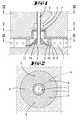
- FIG. 1shows a first exemplary embodiment of a gas-admission element
- FIG. 2shows a section on line II-II
- FIG. 3shows a section on line III-III
- FIG. 4shows a section on line IV-IV
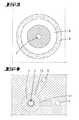
- FIG. 5shows a second exemplary embodiment according to FIG. 1,
- FIGS. 6 - 9show a conversion set with differently configured exchangeable parts.
- FIGS. 1 to 5presents an excerpt from an MOCVD reactor.
- the process chamberbears reference number 1 . It has a base 1 ′ and a ceiling 1 ′′.
- the base 1 ′is the surface of a susceptor 16 which is heated from below by means of high frequency and consists of graphite.
- the gas-admission elementis located in the center of the cylindrically symmetrical process chamber 1 .
- This gas-admission elementhas a central feed line 2 , which opens out in a central outlet opening 3 .
- This central outlet openinglies in an end-side chamber of the gas-admission element.
- the end sideis associated with a quartz body 14 .
- the latterhas a frustoconical wall which forms a gas-guiding surface 15 for the gas flowing out of a peripheral feed line 4 in the axial direction.
- the gas which flows out of the peripheral feed line 4flows into an annular antechamber 8 which is disposed between process-chamber ceiling 1 ′′ and process-chamber base 1 ′ and the rear wall of which is formed by the gas-guiding surface 15 .
- the annular antechamber 8is surrounded by a porous gas-discharge ring 6 , which is produced as quartz frit.
- the second process gas which flows in through the peripheral line 4can emerge through this gas-discharge ring in a homogenized flow profile.
- the annular throttle 7 illustrated in FIG. 5has a greater throttling action.
- the exchangeable parts 14 illustrated in FIGS. 6 to 9can be screwed to the upper part of the gas-admission element, which forms the central feed line 2 and the peripheral feed line 4 , by means of a screw connection 12 .
- a nut 11which carries a plate which forms the process-chamber ceiling 1 ′, is also screwed to this upper portion.
- the lower portion 6 ′ of the gas-discharge ring 6rests on a thin-walled radial annular projection which is formed by the edge portion 10 of the exchangeable part 14 .
- the gas-discharge ring 6is supported on the said plate or on the process-chamber ceiling 1 ′.
- the individual exchangeable parts 14 shown in FIGS. 6 to 9differ from one another substantially in terms of their diameter and in terms of the shape of their guiding surfaces.
- the guiding surfaces 15 of the exchangeable parts shown in FIGS. 6, 7 and 9are substantially in the shape of a rotational hyperboloid.
- the contour line of the gas-guiding surface 15is concave in shape, this surface linking up with the wall of the peripheral line 4 running in the axial direction without any sudden jumps, so that no turbulence develops along the gas-guiding surface 15 .
- the arrows illustrated outside the gas-discharge ring 6indicate the axial flow profile.
- the maximum of this profilelies closer to that end 6 ′ of the gas-discharge ring which is close to the susceptor than to that region of the gas-discharge ring which is close to the process-chamber ceiling 1 ′.
- the result of thisis that the region close to the susceptor and therefore also the edge portion 10 are more strongly cooled by convection.
- the width W of the annular chamber 8decreases in the axial direction from the ceiling 1 ′ to the susceptor 16 .
- the contour line of the gas-guiding surface 15 of the longitudinal sectionis in the form of a straight line, so that the guide surface 15 is frustoconical in shape. This shape is selected for high volumetric flows.
- the susceptor 16is heated from below by means of a high-frequency heating means (not shown).
- the susceptor 16radiates heat which heats the quartz body 14 of the gas-discharge element.
- the first process gaswhich consists of arsine or phosphine and hydrogen, flows through the central outlet opening 3 .
- the arsine or phosphine which emerges through the opening 3decomposes in the gap between the quartz body 14 and the surface of the susceptor 16 .
- the decomposition productsare transported onward in the radial direction.
- TMG or TMI together with hydrogen as second process gasinitially flows out of the peripheral line 4 into the antechamber 8 .
- the gas emerging from the axial line 4flows in laminar fashion along the guiding surface 15 and in the process is diverted through 90°. In the process, it flows over the edge portion 10 . Since the gas flowing out of the line 4 is not preheated, but rather is substantially at room temperature, it has a cooling action with respect to the quartz body 14 . The heat is taken up via the guiding surface 15 . The gas stream has its greatest cooling action in particular where the material thickness of the quartz part 14 is least, namely in the region of the edge portion 10 . This region and in particular the gas-discharge ring portion 6 ′ which is adjacent to the edge portion 10 are therefore cooled most strongly by the gas stream. The process-chamber ceiling 1 ′ is unheated.
- the region 6 ′ of the gas-discharge ring 6would be the hottest, since it is closest to the hot susceptor 16 .
- the region 6 ′ of the gas-discharge ring 6 which is close to the susceptoris kept at a temperature which substantially corresponds to the temperature of the remaining region of the gas-discharge ring 6 .
- This temperatureis higher than the condensation temperature of the arsenic or phosphorus formed in the gap between the susceptor 16 and the quartz body 14 .
- the temperatureis lower than the deposition temperature of the III-V compound.
- the flow parametersshould be set in such a way that the gas-discharge ring as far as possible has a constant temperature over its axial length.
- the profile of the gas-guiding surface 15is matched to the process parameters by substituting an exchangeable part.
Landscapes
- Chemical & Material Sciences (AREA)
- General Chemical & Material Sciences (AREA)
- Chemical Kinetics & Catalysis (AREA)
- Engineering & Computer Science (AREA)
- Materials Engineering (AREA)
- Metallurgy (AREA)
- Organic Chemistry (AREA)
- Mechanical Engineering (AREA)
- Crystallography & Structural Chemistry (AREA)
- Chemical Vapour Deposition (AREA)
Abstract
Description
- This application is a continuation of pending International Patent Application No. PCT/EP01/08139 filed Jul. 14, 2001, which designates the United States and claims priority of pending German Application Nos. 10061671, filed Sep. 22, 2000 and 10064941, filed Dec. 23, 2000.[0001]
- The invention relates firstly to a method for depositing in particular crystalline layers on in particular crystalline substrates, in which at least two process gases are introduced into a process chamber of a reactor separately from one another through a gas-admission element above a heated susceptor, the first process gas flowing through a central line having a central outlet opening, and the second process gas flowing through a line which is peripheral with respect to the central line and has a peripheral outlet opening formed by a gas-permeable gas-discharge ring, which gas-discharge ring surrounds an annular antechamber. The invention also relates to a gas-admission element for a device for depositing in particular crystalline layers on in particular crystalline substrates, by means of which two process gases can be introduced into a process chamber of a reactor separately from one another above a heated susceptor, having a central line with a central end-side outlet opening for the first process gas, and having a line which is peripheral with respect to the central line and has a peripheral outlet opening for the second process gas, which is formed by a gas-permeable gas-discharge ring which surrounds an annular antechamber, the radial width of which decreases toward the free end of the rotationally symmetrical gas-discharge element, on account of a back wall which does not run parallel to the central axis in longitudinal section.[0002]
- A gas-discharge element of this type is known and is used to introduce the reaction gases, in particular for an MOCVD process, into a cylindrically symmetrical process chamber, through which the process gases flow in the radial direction, in order to emerge again through a ring which surrounds the process chamber. Substrates, which are coated with the decomposition products of the reaction gases introduced through the gas-admission element, are disposed in planetary fashion on the susceptor, which is heated from below in particular by means of high frequency. In the region of the gas-admission element or the region which immediately borders it in the radially outward direction, the process chamber has an admission zone in which the gaseous starting materials decompose. In the radially outward direction, this admission zone is adjoined by a deposition zone, within which the decomposition products diffuse toward the substrate, in order to condense there to form a single-crystalline layer.[0003]
- In the known device, the second process gas passes axially into the center of the process chamber through the peripheral feed line. The second process gas used is, for example, TMG or TMI together with a carrier gas, for example hydrogen. The gas comes into contact with a rebounding wall which is formed by the back wall, which runs substantially in the shape of a bell, of the antechamber. The gas-discharge ring has comb-like slots, through which the gas can flow from the antechamber into the admission zone of the process chamber, where it undergoes preliminary decomposition. The metal hydrides, for example phosphine or arsine, enter the process chamber together with a carrier gas through the central feed line. The central opening is disposed close to the heated susceptor. This process gas emerging there flows through a gap between the surface of the heated susceptor and the end face of the free end of the gas-admission element. On account of the thermal radiation of the heated susceptor, the end face of the gas-admission element may heat up. As a corollary effect, the entire quartz body which forms that portion of the gas-admission element which projects into the process chamber is heated up. In particular that portion of the antechamber which is associated with the free end of the gas-admission element and/or the adjoining portion of the gas-discharge ring may in the process reach temperatures at which the metal-organic compounds of gallium or indium supplied through the peripheral line are decomposed, so that deposition of gallium arsenide or indium phosphide occurs in this region of the antechamber or at the gas-discharge ring. These parasitic depositions are disadvantageous.[0004]
- While gallium arsenide and/or indium phosphide are deposited on hot surfaces, if the outer peripheral portion of the end face surrounding the central feed line is too cold, condensation of phosphorus or arsenic may occur there. This too constitutes a drawback.[0005]
- The invention is based on the object of proposing measures, in order on the one hand to counteract parasitic deposition in the region of the peripheral outlet opening and on the other hand to counteract condensation of the V component emerging through the central outlet opening on the radially outer peripheral portion of the end face of the gas-discharge element.[0006]
- The object is achieved by the invention described in the claims.[0007]
Claim 1 proposes that on account of a frustoconical or rotationally hyperboloid shape of a gas-guiding surface formed by the antechamber rear wall, that end portion of the gas-discharge ring which faces the susceptor and/or the radially outer portion of that end side of the gas-discharge element which surrounds the central outlet opening is cooled by the second process gas. In this case, the gas stream which is to be fed to the process chamber from the second feed line is deflected by the gas-guiding surface, in such a manner that it is heated up at the rear wall, which is heated by the radiation of the susceptor, of that portion of the gas-admission element which projects into the process chamber. The heat which is dissipated in the process cools that portion of the antechamber or of the gas-discharge ring which is close to the susceptor. The shape of the gas-guiding surface can be selected in such a way that the cooling occurs only to an extent which is such that the temperature in the end portion of the gas-admission element is kept within a temperature window which is delimited at the bottom by the deposition temperature of the V component and at the top by the deposition temperature of the III-V compound. On account of a porous gas-discharge ring, the pressure in the antechamber is preferably held at a higher level than the process-chamber pressure. Moreover, the use of a porous gas-discharge ring has the advantage compared to the comb-like gas-discharge ring that no turbulence which promotes parasitic deposition develops behind the comb tines. If the gas-discharge element consists, for example, of a quartz frit, the process gas emerges from the gas-discharge ring in homogenized form, the maximum flow of the flow profile lying eccentrically, specifically offset toward the free end of the gas-admission element. The radius of curvature of the guiding surface, which is concave in longitudinal section, is matched to the flow parameters. For higher volumetric flows, the radius of curvature is selected to be greater than for lower volumetric flows. The longitudinal-section contour of the gas-guiding surface may then in particular be a straight line, so that overall the gas-guiding surface is frustoconical in shape. To enable the gas-guiding surface contour to be matched to the various process parameters, such as temperature and overall flow volume, it is provided, according to the invention, that the portion of the gas-admission element which projects into the process chamber is formed as an exchangeable part. This can be screwed to the feed line. It is preferably a quartz part which is also the carrier of the gas-discharge ring. The gas-discharge ring has a gas-guiding surface which is formed by the antechamber rear wall, is configured to be frustoconical or rotationally hyperboloid in shape and links up with the feed line without any step. The gas stream flowing in laminar fashion along the gas-guiding surface effects convective cooling. The increased outlet flow from the gas-discharge ring in the region close to the susceptor also results in a purging effect. In the case of a gallium arsenide deposition process, the temperature of that portion of the gas-admission element which is close to the susceptor is kept within a temperature window between approximately 200° C. and approximately 400° C. - Exemplary embodiments of the inventions are explained below with reference to accompanying drawings, in which:[0008]
- FIG. 1 shows a first exemplary embodiment of a gas-admission element,[0009]
- FIG. 2 shows a section on line II-II,[0010]
- FIG. 3 shows a section on line III-III,[0011]
- FIG. 4 shows a section on line IV-IV,[0012]
- FIG. 5 shows a second exemplary embodiment according to FIG. 1, and[0013]
- FIGS.[0014]6-9 show a conversion set with differently configured exchangeable parts.
- The exemplary embodiment shown in FIGS.[0015]1 to5 presents an excerpt from an MOCVD reactor. The process chamber bears
reference number 1. It has abase 1′ and aceiling 1″. Thebase 1′ is the surface of asusceptor 16 which is heated from below by means of high frequency and consists of graphite. The gas-admission element is located in the center of the cylindricallysymmetrical process chamber 1. This gas-admission element has acentral feed line 2, which opens out in a central outlet opening3. This central outlet opening lies in an end-side chamber of the gas-admission element. The end side is associated with aquartz body 14. The latter has a frustoconical wall which forms a gas-guidingsurface 15 for the gas flowing out of aperipheral feed line 4 in the axial direction. The gas which flows out of theperipheral feed line 4 flows into anannular antechamber 8 which is disposed between process-chamber ceiling 1″ and process-chamber base 1′ and the rear wall of which is formed by the gas-guidingsurface 15. - The[0016]
annular antechamber 8 is surrounded by a porous gas-discharge ring 6, which is produced as quartz frit. The second process gas which flows in through theperipheral line 4 can emerge through this gas-discharge ring in a homogenized flow profile. - Upstream of the[0017]
antechamber 8 there is anannular throttle 7 with a multiplicity ofpassage openings 9. Upstream of theannular throttle 7 there is in turn a mixing chamber, into which twogases feed lines reference numerals - On account of its increased thickness, the[0018]
annular throttle 7 illustrated in FIG. 5 has a greater throttling action. - The[0019]
exchangeable parts 14 illustrated in FIGS.6 to9 can be screwed to the upper part of the gas-admission element, which forms thecentral feed line 2 and theperipheral feed line 4, by means of ascrew connection 12. Anut 11, which carries a plate which forms the process-chamber ceiling 1′, is also screwed to this upper portion. Thelower portion 6′ of the gas-discharge ring 6 rests on a thin-walled radial annular projection which is formed by theedge portion 10 of theexchangeable part 14. At the top, the gas-discharge ring 6 is supported on the said plate or on the process-chamber ceiling 1′. - The individual[0020]
exchangeable parts 14 shown in FIGS.6 to9 differ from one another substantially in terms of their diameter and in terms of the shape of their guiding surfaces. The guiding surfaces15 of the exchangeable parts shown in FIGS. 6, 7 and9 are substantially in the shape of a rotational hyperboloid. In the longitudinal section plane illustrated, the contour line of the gas-guidingsurface 15 is concave in shape, this surface linking up with the wall of theperipheral line 4 running in the axial direction without any sudden jumps, so that no turbulence develops along the gas-guidingsurface 15. The arrows illustrated outside the gas-discharge ring 6 indicate the axial flow profile. It can be seen that the maximum of this profile lies closer to thatend 6′ of the gas-discharge ring which is close to the susceptor than to that region of the gas-discharge ring which is close to the process-chamber ceiling 1′. The result of this is that the region close to the susceptor and therefore also theedge portion 10 are more strongly cooled by convection. In all the exemplary embodiments, the width W of theannular chamber 8 decreases in the axial direction from theceiling 1′ to thesusceptor 16. - In the exemplary embodiment illustrated in FIG. 8, the contour line of the gas-guiding[0021]
surface 15 of the longitudinal section is in the form of a straight line, so that theguide surface 15 is frustoconical in shape. This shape is selected for high volumetric flows. - The[0022]
susceptor 16 is heated from below by means of a high-frequency heating means (not shown). Thesusceptor 16 radiates heat which heats thequartz body 14 of the gas-discharge element. The first process gas, which consists of arsine or phosphine and hydrogen, flows through thecentral outlet opening 3. The arsine or phosphine which emerges through theopening 3 decomposes in the gap between thequartz body 14 and the surface of thesusceptor 16. The decomposition products are transported onward in the radial direction. TMG or TMI together with hydrogen as second process gas initially flows out of theperipheral line 4 into theantechamber 8. The gas emerging from theaxial line 4 flows in laminar fashion along the guidingsurface 15 and in the process is diverted through 90°. In the process, it flows over theedge portion 10. Since the gas flowing out of theline 4 is not preheated, but rather is substantially at room temperature, it has a cooling action with respect to thequartz body 14. The heat is taken up via the guidingsurface 15. The gas stream has its greatest cooling action in particular where the material thickness of thequartz part 14 is least, namely in the region of theedge portion 10. This region and in particular the gas-discharge ring portion 6′ which is adjacent to theedge portion 10 are therefore cooled most strongly by the gas stream. The process-chamber ceiling 1′ is unheated. Accordingly, without a cooling gas stream, theregion 6′ of the gas-discharge ring 6 would be the hottest, since it is closest to thehot susceptor 16. On account of the convective cooling of the process gas emerging from theline 4, however, theregion 6′ of the gas-discharge ring 6 which is close to the susceptor is kept at a temperature which substantially corresponds to the temperature of the remaining region of the gas-discharge ring 6. This temperature is higher than the condensation temperature of the arsenic or phosphorus formed in the gap between the susceptor16 and thequartz body 14. However, the temperature is lower than the deposition temperature of the III-V compound. - The flow parameters should be set in such a way that the gas-discharge ring as far as possible has a constant temperature over its axial length.[0023]
- The profile of the gas-guiding[0024]
surface 15 is matched to the process parameters by substituting an exchangeable part. - All features disclosed are (inherently) pertinent to the invention. The disclosure content of the associated/appended priority documents (copy of the prior application) is hereby incorporated in its entirety in the disclosure of the application, partly with a view to incorporating features of these documents in claims of the present application.[0025]
Claims (10)
1. Method for depositing in particular crystalline layers on in particular crystalline substrates, in which at least two process gases are introduced into a process chamber (1) of a reactor separately from one another through a gas-admission element above a heated susceptor (16), the first process gas (16) flowing through a central line (2) having a central outlet opening (3), and the second process gas flowing through a line (4) which is peripheral with respect to the central line and has a peripheral outlet opening formed by a gas-permeable gas-discharge ring (6), which gas-discharge ring (6) surrounds an annular antechamber (8), characterized in that, on account of a frustoconical or rotationally hyperboloid shape of a gas-guiding surface formed by the antechamber rear wall (15), that end portion (6′) of the gas-discharge ring (6) which faces the susceptor and/or the radially outer portion of that end side of the gas-discharge element which surrounds the central outlet opening (3) is cooled by the second process gas.
2. Method according toclaim 1 or in particular according thereto, characterized in that the pressure in the antechamber (8) is greater than in the process chamber (1), on account of a porous gas-discharge ring (6).
3. Method according to one or more of the preceding claims or in particular according thereto, characterized in that the radius of curvature of the guiding surface (15), which is concave in longitudinal section, is selected to be larger for higher volumetric gas flows.
4. Method according to one or more of the preceding claims or in particular according thereto, characterized in that the maximum of the gas stream emerging from the gas-discharge ring (6), in the longitudinal section plane, lies eccentrically offset toward the free end (6′).
5. Method according to one or more of the preceding claims or in particular according thereto, characterized in that the flow parameters and the longitudinal-section contour line of the gas-guiding surface (16) are matched to one another in such a manner that the temperature of that portion of the gas-discharge element which is adjacent to the hot susceptor (16) is greater than the condensation temperature of the arsenic or phosphorus which is formed by pyrolytic decomposition from phosphine or arsine and is lower than the deposition temperature of gallium arsenide or indium phosphide.
6. Gas-admission element for a device for depositing in particular crystalline layers on in particular layers on in particular crystalline substrates, by means of which two process gases can be introduced into a process chamber (1) of a reactor separately from one another above a heatable susceptor (16), having a central line (2) with a central end-side outlet opening (3) for the first process gas, and having a line (4) which is peripheral with respect to the central line and has a peripheral outlet opening for the second process gas, which is formed by a gas-permeable gas-discharge ring (6) which surrounds an annular antechamber (8), the radial width (W) of which decreases toward the free end (6′) of the rotationally symmetrical gas-discharge element, on account of a back wall (15) which does not run parallel to the central axis in longitudinal section, characterized by a frustoconical or rotationally hyperboloid-shaped gas-guiding surface (15), which is formed by the antechamber rear wall, for convective cooling of that portion (6′) of the gas-discharge ring (6) which is close to the susceptor, by means of the gas flowing along the gas-guiding surface (15).
7. Gas-admission element according toclaim 6 or in particular according thereto, characterized in that the gas-discharge ring (6) consists of porous material and in particular is a quartz frit.
8. Gas-admission element according to claims6 and7 or in particular according thereto, characterized in that the gas-guiding surface (15) is associated with an exchangeable part (14).
9. Gas-admission element according toclaim 6 ,7 and8 or in particular according thereto, characterized in that the gas-guiding surface (15) links up with the feed line (4) without there being a step.
10. Gas-admission element according toclaim 6 ,7,8 and9 or in particular according thereto, characterized in that the exchangeable part (14) can be screwed to the feed line (2,4) or can be connected to the feed line (2,4) by way of a bayonet connection.
Applications Claiming Priority (5)
| Application Number | Priority Date | Filing Date | Title |
|---|---|---|---|
| DE10061671.2 | 2000-09-22 | ||
| DE10061671 | 2000-09-22 | ||
| DE10064941.6 | 2000-12-23 | ||
| DE10064941ADE10064941A1 (en) | 2000-09-22 | 2000-12-23 | Gas inlet element |
| PCT/EP2001/008139WO2002024985A1 (en) | 2000-09-22 | 2001-07-14 | Gas inlet mechanism for cvd-method and device |
Related Parent Applications (1)
| Application Number | Title | Priority Date | Filing Date |
|---|---|---|---|
| PCT/EP2001/008139ContinuationWO2002024985A1 (en) | 2000-09-22 | 2001-07-14 | Gas inlet mechanism for cvd-method and device |
Publications (2)
| Publication Number | Publication Date |
|---|---|
| US20030177977A1true US20030177977A1 (en) | 2003-09-25 |
| US7294207B2 US7294207B2 (en) | 2007-11-13 |
Family
ID=26007933
Family Applications (1)
| Application Number | Title | Priority Date | Filing Date |
|---|---|---|---|
| US10/395,948Expired - Fee RelatedUS7294207B2 (en) | 2000-09-22 | 2003-03-24 | Gas-admission element for CVD processes, and device |
Country Status (5)
| Country | Link |
|---|---|
| US (1) | US7294207B2 (en) |
| EP (1) | EP1322801B1 (en) |
| AU (1) | AU2001283944A1 (en) |
| TW (1) | TW555900B (en) |
| WO (1) | WO2002024985A1 (en) |
Cited By (22)
| Publication number | Priority date | Publication date | Assignee | Title |
|---|---|---|---|---|
| US20040005731A1 (en)* | 2000-09-01 | 2004-01-08 | Holger Jurgensen | Device and method for the depostion of, in particular, crystalline layers on, in particular, crystalline substrates |
| WO2005080631A1 (en)* | 2004-02-25 | 2005-09-01 | Aixtron Ag | Inlet system for an mocvd reactor |
| US20060130756A1 (en)* | 2004-12-17 | 2006-06-22 | Applied Materials, Inc., A Delaware Corporation | Self-cooling gas delivery apparatus under high vacuum for high density plasma applications |
| US20060196603A1 (en)* | 2005-03-07 | 2006-09-07 | Applied Materials, Inc. | Gas baffle and distributor for semiconductor processing chamber |
| WO2006094824A1 (en)* | 2005-03-11 | 2006-09-14 | Centrotherm Thermal Solutions Gmbh + Co. Kg | Gas-tight connecting element comprising a bayonet closure |
| US20070234956A1 (en)* | 2006-04-05 | 2007-10-11 | Dalton Jeremie J | Method and apparatus for providing uniform gas delivery to a reactor |
| US7294207B2 (en)* | 2000-09-22 | 2007-11-13 | Aixtron Ag | Gas-admission element for CVD processes, and device |
| US20080121179A1 (en)* | 2006-11-28 | 2008-05-29 | Applied Materials, Inc. | Gas baffle and distributor for semiconductor processing chamber |
| US20080121177A1 (en)* | 2006-11-28 | 2008-05-29 | Applied Materials, Inc. | Dual top gas feed through distributor for high density plasma chamber |
| US20080121178A1 (en)* | 2006-11-28 | 2008-05-29 | Applied Materials, Inc. | Dual top gas feed through distributor for high density plasma chamber |
| US20080308040A1 (en)* | 2005-11-25 | 2008-12-18 | Martin Dauelsberg | Cvd Reactor Comprising a Gas Inlet Member |
| US20090093129A1 (en)* | 2006-11-28 | 2009-04-09 | Applied Materials, Inc. | Gas Baffle and Distributor for Semiconductor Processing Chamber |
| US20110180001A1 (en)* | 2010-01-26 | 2011-07-28 | Japan Pionics Co., Ltd. | Vapor phase epitaxy apparatus of group iii nitride semiconductor |
| US20120111271A1 (en)* | 2007-10-11 | 2012-05-10 | Begarney Michael J | Chemical vapor deposition reactor |
| US20120164843A1 (en)* | 2007-11-20 | 2012-06-28 | Soitec | Transfer of high temperature wafers |
| CN105765115A (en)* | 2013-09-02 | 2016-07-13 | 原子能及能源替代委员会 | Method and device for treating the free surface of a material |
| US10403515B2 (en)* | 2015-09-24 | 2019-09-03 | Applied Materials, Inc. | Loadlock integrated bevel etcher system |
| CN112342529A (en)* | 2020-09-24 | 2021-02-09 | 杭州盾源聚芯半导体科技有限公司 | Injection pipe with connector |
| CN114105679A (en)* | 2021-11-25 | 2022-03-01 | 西安鑫垚陶瓷复合材料有限公司 | Chemical vapor infiltration flow guide equipment and method for preparing ceramic composite pipe fitting by using same |
| CN114164412A (en)* | 2020-09-10 | 2022-03-11 | 鑫天虹(厦门)科技有限公司 | Sprinkler structure of semiconductor atomic layer deposition device |
| CN116334596A (en)* | 2021-12-23 | 2023-06-27 | 湖南红太阳光电科技有限公司 | Glow discharge device of PECVD (plasma enhanced chemical vapor deposition) equipment |
| USD1080812S1 (en) | 2022-08-29 | 2025-06-24 | Applied Materials, Inc. | Gas mixer |
Families Citing this family (6)
| Publication number | Priority date | Publication date | Assignee | Title |
|---|---|---|---|---|
| DE102005045582B3 (en) | 2005-09-23 | 2007-03-29 | Fraunhofer-Gesellschaft zur Förderung der angewandten Forschung e.V. | Apparatus and method for continuous vapor deposition under atmospheric pressure and their use |
| TW201239129A (en)* | 2010-12-20 | 2012-10-01 | Samsung Led Co Ltd | Chemical vapor deposition apparatus and method of manufacturing LED using the same |
| TWI473903B (en) | 2013-02-23 | 2015-02-21 | Hermes Epitek Corp | Gas Injector and Cover Plate Assembly for Semiconductor Equipment |
| US10407771B2 (en)* | 2014-10-06 | 2019-09-10 | Applied Materials, Inc. | Atomic layer deposition chamber with thermal lid |
| US20240254653A1 (en)* | 2023-01-26 | 2024-08-01 | Applied Materials, Inc. | Cell architectural structures for enhanced thermal management in epitaxial growth processing chamber |
| CN116791065B (en)* | 2023-07-03 | 2024-06-14 | 拓荆科技(上海)有限公司 | Diffusion member and semiconductor process equipment |
Citations (38)
| Publication number | Priority date | Publication date | Assignee | Title |
|---|---|---|---|---|
| US3674453A (en)* | 1968-08-16 | 1972-07-04 | Pilkington Brothers Ltd | Production of float glass having an oxidized metal-modified surface |
| US3757733A (en)* | 1971-10-27 | 1973-09-11 | Texas Instruments Inc | Radial flow reactor |
| US4033287A (en)* | 1976-01-22 | 1977-07-05 | Bell Telephone Laboratories, Incorporated | Radial flow reactor including glow discharge limiting shield |
| USRE30244E (en)* | 1976-01-22 | 1980-04-01 | Bell Telephone Laboratories, Incorporated | Radial flow reactor including glow discharge limitting shield |
| US4207137A (en)* | 1979-04-13 | 1980-06-10 | Bell Telephone Laboratories, Incorporated | Method of controlling a plasma etching process by monitoring the impedance changes of the RF power |
| US4533410A (en)* | 1982-10-19 | 1985-08-06 | Matsushita Electric Industrial Co., Ltd. | Process of vapor phase epitaxy of compound semiconductors |
| US4590042A (en)* | 1984-12-24 | 1986-05-20 | Tegal Corporation | Plasma reactor having slotted manifold |
| US4612077A (en)* | 1985-07-29 | 1986-09-16 | The Perkin-Elmer Corporation | Electrode for plasma etching system |
| US4778559A (en)* | 1986-10-15 | 1988-10-18 | Advantage Production Technology | Semiconductor substrate heater and reactor process and apparatus |
| US4793975A (en)* | 1985-05-20 | 1988-12-27 | Tegal Corporation | Plasma Reactor with removable insert |
| US4993358A (en)* | 1989-07-28 | 1991-02-19 | Watkins-Johnson Company | Chemical vapor deposition reactor and method of operation |
| US5027746A (en)* | 1988-03-22 | 1991-07-02 | U.S. Philips Corporation | Epitaxial reactor having a wall which is protected from deposits |
| US5275976A (en)* | 1990-12-27 | 1994-01-04 | Texas Instruments Incorporated | Process chamber purge module for semiconductor processing equipment |
| US5366557A (en)* | 1990-06-18 | 1994-11-22 | At&T Bell Laboratories | Method and apparatus for forming integrated circuit layers |
| US5422139A (en)* | 1990-04-12 | 1995-06-06 | Balzers Aktiengesellschaft | Method for a reactive surface treatment of a workpiece and a treatment chamber for practicing such method |
| US5849088A (en)* | 1998-01-16 | 1998-12-15 | Watkins-Johnson Company | Free floating shield |
| US5954881A (en)* | 1997-01-28 | 1999-09-21 | Northrop Grumman Corporation | Ceiling arrangement for an epitaxial growth reactor |
| US6007633A (en)* | 1997-04-09 | 1999-12-28 | Tokyo Electron Limited | Single-substrate-processing apparatus in semiconductor processing system |
| US6039812A (en)* | 1996-10-21 | 2000-03-21 | Abb Research Ltd. | Device for epitaxially growing objects and method for such a growth |
| US6056824A (en)* | 1998-01-16 | 2000-05-02 | Silicon Valley Group Thermal Systems | Free floating shield and semiconductor processing system |
| US6246030B1 (en)* | 1998-07-22 | 2001-06-12 | Tokyo Electron Limited | Heat processing method and apparatus |
| US6352592B1 (en)* | 1998-01-16 | 2002-03-05 | Silicon Valley Group, Thermal Systems Llc | Free floating shield and semiconductor processing system |
| US6444042B1 (en)* | 1999-02-25 | 2002-09-03 | Hyundai Electronics Industries Co., Ltd. | Gas injection system for chemical vapor deposition device |
| US6487986B1 (en)* | 1998-09-12 | 2002-12-03 | Unaxis Deutschland Holding Gmbh | Device for the plasma deposition of a polycrystalline diamond |
| US6537418B1 (en)* | 1997-09-19 | 2003-03-25 | Siemens Aktiengesellschaft | Spatially uniform gas supply and pump configuration for large wafer diameters |
| US6539890B1 (en)* | 1998-05-28 | 2003-04-01 | Nano Scale Surface Systems, Inc. | Multiple source deposition plasma apparatus |
| US6576060B1 (en)* | 1999-05-21 | 2003-06-10 | Asml Us, Inc. | Protective gas shield apparatus |
| US6592771B1 (en)* | 1999-04-08 | 2003-07-15 | Sony Corporation | Vapor-phase processing method and apparatus therefor |
| US6676758B2 (en)* | 2000-08-09 | 2004-01-13 | Itt Manufacturing Enterprises, Inc. | Gas collector for epitaxial reactor |
| US6737812B2 (en)* | 2001-09-21 | 2004-05-18 | Tokyo Electron Limited | Plasma processing apparatus |
| US20040134429A1 (en)* | 1999-01-22 | 2004-07-15 | Hideo Yamanaka | Film forming method and film forming apparatus |
| US6770137B2 (en)* | 2000-11-10 | 2004-08-03 | Denso Corporation | Manufacturing method for producing silicon carbide crystal using source gases and apparatus for the same |
| US6786973B2 (en)* | 2000-09-22 | 2004-09-07 | Aixtron Ag | Method for depositing in particular crystalline layers, gas-admission element and device for carrying out the method |
| US20040182316A1 (en)* | 2002-12-26 | 2004-09-23 | Reiki Watanabe | Processing equipment and processing method |
| US6830618B2 (en)* | 2000-11-10 | 2004-12-14 | Denso Corporation | Manufacturing method for producing silicon carbide crystal using source gases and apparatus for the same |
| US20050000441A1 (en)* | 2001-10-30 | 2005-01-06 | Johannes Kaeppeler | Process and device for depositing in particular crystalline layers on in particular crystalline substrates |
| US6849241B2 (en)* | 2000-02-04 | 2005-02-01 | Aixtron Ag. | Device and method for depositing one or more layers on a substrate |
| US6890386B2 (en)* | 2001-07-13 | 2005-05-10 | Aviza Technology, Inc. | Modular injector and exhaust assembly |
Family Cites Families (7)
| Publication number | Priority date | Publication date | Assignee | Title |
|---|---|---|---|---|
| GB1056430A (en)* | 1962-11-13 | 1967-01-25 | Texas Instruments Inc | Epitaxial process and apparatus for semiconductors |
| FR2628984B1 (en)* | 1988-03-22 | 1990-12-28 | Labo Electronique Physique | PLANETARY EPITAXY REACTOR |
| WO1998045501A1 (en)* | 1997-04-10 | 1998-10-15 | Koninklijke Philips Electronics N.V. | Method of manufacturing a semiconductor device and a device for applying such a method |
| DE10043601A1 (en)* | 2000-09-01 | 2002-03-14 | Aixtron Ag | Device and method for depositing, in particular, crystalline layers on, in particular, crystalline substrates |
| EP1322801B1 (en)* | 2000-09-22 | 2010-01-06 | Aixtron Ag | Cvd-method and gas inlet mechanism for carrying out the method |
| DE10133914A1 (en)* | 2001-07-12 | 2003-01-23 | Aixtron Ag | Apparatus to deposit crystalline layers on semiconductor wafers comprises rotating wafer holders mounted on rotating mounting forming floor of process chamber whose roof contains central gas inlet |
| DE10247921A1 (en)* | 2002-10-10 | 2004-04-22 | Aixtron Ag | Hydride vapor phase epitaxy reactor, to produce pseudo-substrates for electronic components, deposits layers of crystalline substrates from a gas phase with increased growth rates |
- 2001
- 2001-07-14EPEP01962856Apatent/EP1322801B1/ennot_activeExpired - Lifetime
- 2001-07-14AUAU2001283944Apatent/AU2001283944A1/ennot_activeAbandoned
- 2001-07-14WOPCT/EP2001/008139patent/WO2002024985A1/enactiveApplication Filing
- 2001-09-10TWTW090122330Apatent/TW555900B/ennot_activeIP Right Cessation
- 2003
- 2003-03-24USUS10/395,948patent/US7294207B2/ennot_activeExpired - Fee Related
Patent Citations (38)
| Publication number | Priority date | Publication date | Assignee | Title |
|---|---|---|---|---|
| US3674453A (en)* | 1968-08-16 | 1972-07-04 | Pilkington Brothers Ltd | Production of float glass having an oxidized metal-modified surface |
| US3757733A (en)* | 1971-10-27 | 1973-09-11 | Texas Instruments Inc | Radial flow reactor |
| US4033287A (en)* | 1976-01-22 | 1977-07-05 | Bell Telephone Laboratories, Incorporated | Radial flow reactor including glow discharge limiting shield |
| USRE30244E (en)* | 1976-01-22 | 1980-04-01 | Bell Telephone Laboratories, Incorporated | Radial flow reactor including glow discharge limitting shield |
| US4207137A (en)* | 1979-04-13 | 1980-06-10 | Bell Telephone Laboratories, Incorporated | Method of controlling a plasma etching process by monitoring the impedance changes of the RF power |
| US4533410A (en)* | 1982-10-19 | 1985-08-06 | Matsushita Electric Industrial Co., Ltd. | Process of vapor phase epitaxy of compound semiconductors |
| US4590042A (en)* | 1984-12-24 | 1986-05-20 | Tegal Corporation | Plasma reactor having slotted manifold |
| US4793975A (en)* | 1985-05-20 | 1988-12-27 | Tegal Corporation | Plasma Reactor with removable insert |
| US4612077A (en)* | 1985-07-29 | 1986-09-16 | The Perkin-Elmer Corporation | Electrode for plasma etching system |
| US4778559A (en)* | 1986-10-15 | 1988-10-18 | Advantage Production Technology | Semiconductor substrate heater and reactor process and apparatus |
| US5027746A (en)* | 1988-03-22 | 1991-07-02 | U.S. Philips Corporation | Epitaxial reactor having a wall which is protected from deposits |
| US4993358A (en)* | 1989-07-28 | 1991-02-19 | Watkins-Johnson Company | Chemical vapor deposition reactor and method of operation |
| US5422139A (en)* | 1990-04-12 | 1995-06-06 | Balzers Aktiengesellschaft | Method for a reactive surface treatment of a workpiece and a treatment chamber for practicing such method |
| US5366557A (en)* | 1990-06-18 | 1994-11-22 | At&T Bell Laboratories | Method and apparatus for forming integrated circuit layers |
| US5275976A (en)* | 1990-12-27 | 1994-01-04 | Texas Instruments Incorporated | Process chamber purge module for semiconductor processing equipment |
| US6039812A (en)* | 1996-10-21 | 2000-03-21 | Abb Research Ltd. | Device for epitaxially growing objects and method for such a growth |
| US5954881A (en)* | 1997-01-28 | 1999-09-21 | Northrop Grumman Corporation | Ceiling arrangement for an epitaxial growth reactor |
| US6007633A (en)* | 1997-04-09 | 1999-12-28 | Tokyo Electron Limited | Single-substrate-processing apparatus in semiconductor processing system |
| US6537418B1 (en)* | 1997-09-19 | 2003-03-25 | Siemens Aktiengesellschaft | Spatially uniform gas supply and pump configuration for large wafer diameters |
| US5849088A (en)* | 1998-01-16 | 1998-12-15 | Watkins-Johnson Company | Free floating shield |
| US6056824A (en)* | 1998-01-16 | 2000-05-02 | Silicon Valley Group Thermal Systems | Free floating shield and semiconductor processing system |
| US6352592B1 (en)* | 1998-01-16 | 2002-03-05 | Silicon Valley Group, Thermal Systems Llc | Free floating shield and semiconductor processing system |
| US6539890B1 (en)* | 1998-05-28 | 2003-04-01 | Nano Scale Surface Systems, Inc. | Multiple source deposition plasma apparatus |
| US6246030B1 (en)* | 1998-07-22 | 2001-06-12 | Tokyo Electron Limited | Heat processing method and apparatus |
| US6487986B1 (en)* | 1998-09-12 | 2002-12-03 | Unaxis Deutschland Holding Gmbh | Device for the plasma deposition of a polycrystalline diamond |
| US20040134429A1 (en)* | 1999-01-22 | 2004-07-15 | Hideo Yamanaka | Film forming method and film forming apparatus |
| US6444042B1 (en)* | 1999-02-25 | 2002-09-03 | Hyundai Electronics Industries Co., Ltd. | Gas injection system for chemical vapor deposition device |
| US6592771B1 (en)* | 1999-04-08 | 2003-07-15 | Sony Corporation | Vapor-phase processing method and apparatus therefor |
| US6576060B1 (en)* | 1999-05-21 | 2003-06-10 | Asml Us, Inc. | Protective gas shield apparatus |
| US6849241B2 (en)* | 2000-02-04 | 2005-02-01 | Aixtron Ag. | Device and method for depositing one or more layers on a substrate |
| US6676758B2 (en)* | 2000-08-09 | 2004-01-13 | Itt Manufacturing Enterprises, Inc. | Gas collector for epitaxial reactor |
| US6786973B2 (en)* | 2000-09-22 | 2004-09-07 | Aixtron Ag | Method for depositing in particular crystalline layers, gas-admission element and device for carrying out the method |
| US6770137B2 (en)* | 2000-11-10 | 2004-08-03 | Denso Corporation | Manufacturing method for producing silicon carbide crystal using source gases and apparatus for the same |
| US6830618B2 (en)* | 2000-11-10 | 2004-12-14 | Denso Corporation | Manufacturing method for producing silicon carbide crystal using source gases and apparatus for the same |
| US6890386B2 (en)* | 2001-07-13 | 2005-05-10 | Aviza Technology, Inc. | Modular injector and exhaust assembly |
| US6737812B2 (en)* | 2001-09-21 | 2004-05-18 | Tokyo Electron Limited | Plasma processing apparatus |
| US20050000441A1 (en)* | 2001-10-30 | 2005-01-06 | Johannes Kaeppeler | Process and device for depositing in particular crystalline layers on in particular crystalline substrates |
| US20040182316A1 (en)* | 2002-12-26 | 2004-09-23 | Reiki Watanabe | Processing equipment and processing method |
Cited By (41)
| Publication number | Priority date | Publication date | Assignee | Title |
|---|---|---|---|---|
| US20040005731A1 (en)* | 2000-09-01 | 2004-01-08 | Holger Jurgensen | Device and method for the depostion of, in particular, crystalline layers on, in particular, crystalline substrates |
| US7147718B2 (en)* | 2000-09-01 | 2006-12-12 | Aixtron Ag | Device and method for the deposition of, in particular, crystalline layers on, in particular, crystalline substrates |
| US7294207B2 (en)* | 2000-09-22 | 2007-11-13 | Aixtron Ag | Gas-admission element for CVD processes, and device |
| WO2005080631A1 (en)* | 2004-02-25 | 2005-09-01 | Aixtron Ag | Inlet system for an mocvd reactor |
| US7625448B2 (en) | 2004-02-25 | 2009-12-01 | Aixtron Ag | Inlet system for an MOCVD reactor |
| US20080069953A1 (en)* | 2004-02-25 | 2008-03-20 | Aixtron Ag | Inlet system for an MOCVD reactor |
| US20060130756A1 (en)* | 2004-12-17 | 2006-06-22 | Applied Materials, Inc., A Delaware Corporation | Self-cooling gas delivery apparatus under high vacuum for high density plasma applications |
| US7510624B2 (en) | 2004-12-17 | 2009-03-31 | Applied Materials, Inc. | Self-cooling gas delivery apparatus under high vacuum for high density plasma applications |
| US20060196603A1 (en)* | 2005-03-07 | 2006-09-07 | Applied Materials, Inc. | Gas baffle and distributor for semiconductor processing chamber |
| US7722719B2 (en)* | 2005-03-07 | 2010-05-25 | Applied Materials, Inc. | Gas baffle and distributor for semiconductor processing chamber |
| WO2006094824A1 (en)* | 2005-03-11 | 2006-09-14 | Centrotherm Thermal Solutions Gmbh + Co. Kg | Gas-tight connecting element comprising a bayonet closure |
| US20080308040A1 (en)* | 2005-11-25 | 2008-12-18 | Martin Dauelsberg | Cvd Reactor Comprising a Gas Inlet Member |
| US8152924B2 (en)* | 2005-11-25 | 2012-04-10 | Aixtron Inc. | CVD reactor comprising a gas inlet member |
| TWI414624B (en)* | 2005-11-25 | 2013-11-11 | Aixtron Ag | Cvd-reaktor mit einem gaseinlassorgan |
| US7981472B2 (en) | 2006-04-05 | 2011-07-19 | Aixtron, Inc. | Methods of providing uniform gas delivery to a reactor |
| US20070234956A1 (en)* | 2006-04-05 | 2007-10-11 | Dalton Jeremie J | Method and apparatus for providing uniform gas delivery to a reactor |
| US20090324829A1 (en)* | 2006-04-05 | 2009-12-31 | Dalton Jeremie J | Method and apparatus for providing uniform gas delivery to a reactor |
| US7758698B2 (en) | 2006-11-28 | 2010-07-20 | Applied Materials, Inc. | Dual top gas feed through distributor for high density plasma chamber |
| US7740706B2 (en) | 2006-11-28 | 2010-06-22 | Applied Materials, Inc. | Gas baffle and distributor for semiconductor processing chamber |
| US20090042407A1 (en)* | 2006-11-28 | 2009-02-12 | Applied Materials, Inc. | Dual Top Gas Feed Through Distributor for High Density Plasma Chamber |
| US7799704B2 (en) | 2006-11-28 | 2010-09-21 | Applied Materials, Inc. | Gas baffle and distributor for semiconductor processing chamber |
| US20080121178A1 (en)* | 2006-11-28 | 2008-05-29 | Applied Materials, Inc. | Dual top gas feed through distributor for high density plasma chamber |
| US20090093129A1 (en)* | 2006-11-28 | 2009-04-09 | Applied Materials, Inc. | Gas Baffle and Distributor for Semiconductor Processing Chamber |
| US20080121177A1 (en)* | 2006-11-28 | 2008-05-29 | Applied Materials, Inc. | Dual top gas feed through distributor for high density plasma chamber |
| US20080121179A1 (en)* | 2006-11-28 | 2008-05-29 | Applied Materials, Inc. | Gas baffle and distributor for semiconductor processing chamber |
| US8778079B2 (en)* | 2007-10-11 | 2014-07-15 | Valence Process Equipment, Inc. | Chemical vapor deposition reactor |
| US20120111271A1 (en)* | 2007-10-11 | 2012-05-10 | Begarney Michael J | Chemical vapor deposition reactor |
| US20120164843A1 (en)* | 2007-11-20 | 2012-06-28 | Soitec | Transfer of high temperature wafers |
| US8455370B2 (en)* | 2007-11-20 | 2013-06-04 | Soitec | Transfer of high temperature wafers |
| US20110180001A1 (en)* | 2010-01-26 | 2011-07-28 | Japan Pionics Co., Ltd. | Vapor phase epitaxy apparatus of group iii nitride semiconductor |
| US8679254B2 (en)* | 2010-01-26 | 2014-03-25 | Japan Pionics Co., Ltd. | Vapor phase epitaxy apparatus of group III nitride semiconductor |
| CN105765115A (en)* | 2013-09-02 | 2016-07-13 | 原子能及能源替代委员会 | Method and device for treating the free surface of a material |
| US10112838B2 (en) | 2013-09-02 | 2018-10-30 | Commissariat A L'energie Atomique Et Aux Energies Alternatives | Method and device for treating the free surface of a material |
| US10403515B2 (en)* | 2015-09-24 | 2019-09-03 | Applied Materials, Inc. | Loadlock integrated bevel etcher system |
| US10636684B2 (en)* | 2015-09-24 | 2020-04-28 | Applied Materials, Inc. | Loadlock integrated bevel etcher system |
| US11031262B2 (en)* | 2015-09-24 | 2021-06-08 | Applied Materials, Inc. | Loadlock integrated bevel etcher system |
| CN114164412A (en)* | 2020-09-10 | 2022-03-11 | 鑫天虹(厦门)科技有限公司 | Sprinkler structure of semiconductor atomic layer deposition device |
| CN112342529A (en)* | 2020-09-24 | 2021-02-09 | 杭州盾源聚芯半导体科技有限公司 | Injection pipe with connector |
| CN114105679A (en)* | 2021-11-25 | 2022-03-01 | 西安鑫垚陶瓷复合材料有限公司 | Chemical vapor infiltration flow guide equipment and method for preparing ceramic composite pipe fitting by using same |
| CN116334596A (en)* | 2021-12-23 | 2023-06-27 | 湖南红太阳光电科技有限公司 | Glow discharge device of PECVD (plasma enhanced chemical vapor deposition) equipment |
| USD1080812S1 (en) | 2022-08-29 | 2025-06-24 | Applied Materials, Inc. | Gas mixer |
Also Published As
| Publication number | Publication date |
|---|---|
| WO2002024985A1 (en) | 2002-03-28 |
| AU2001283944A1 (en) | 2002-04-02 |
| US7294207B2 (en) | 2007-11-13 |
| EP1322801A1 (en) | 2003-07-02 |
| EP1322801B1 (en) | 2010-01-06 |
| TW555900B (en) | 2003-10-01 |
Similar Documents
| Publication | Publication Date | Title |
|---|---|---|
| US7294207B2 (en) | Gas-admission element for CVD processes, and device | |
| US7709398B2 (en) | Process and apparatus for depositing semiconductor layers using two process gases, one of which is preconditioned | |
| JP2012519239A (en) | Gas injector for a CVD system with a gas injector | |
| US11286566B2 (en) | Apparatus for deposition of a III-V semiconductor layer | |
| US5916369A (en) | Gas inlets for wafer processing chamber | |
| US5304247A (en) | Apparatus for depositing compound semiconductor crystal | |
| US6852168B2 (en) | Reactor for depositing thin film on wafer | |
| TWI570258B (en) | Gas distribution showerhead with high emissivity surface | |
| JP5837178B2 (en) | Liner assembly for chemical vapor deposition chambers | |
| US6500734B2 (en) | Gas inlets for wafer processing chamber | |
| EP0637058A1 (en) | Gas inlets for wafer processing chamber | |
| EP1271607A2 (en) | Chemical vapor deposition apparatus and method | |
| US6811614B2 (en) | CVD reactor with substrate holder which is rotatably driven and mounted by a gas stream | |
| JP4303966B2 (en) | In particular, a method for depositing a crystalline film and an apparatus for carrying out the method | |
| KR100797227B1 (en) | Method and gas inlet element for depositing a crystal layer on a crystal substrate | |
| US9481944B2 (en) | Gas injectors including a funnel- or wedge-shaped channel for chemical vapor deposition (CVD) systems and CVD systems with the same | |
| CN103320770A (en) | Gas spraying head and vapor phase deposition reaction cavity | |
| EP1076732B1 (en) | Injector for reactor | |
| US20030127050A1 (en) | Chemical vapor deposition apparatus | |
| EP0653500A1 (en) | CVD reactor for improved film thickness uniformity deposition | |
| JPH11152572A (en) | Gas expanding flow regulator | |
| JPH02109323A (en) | Barrel type vapor phase growth equipment | |
| JPH02268419A (en) | Manufacture of semiconductor |
Legal Events
| Date | Code | Title | Description |
|---|---|---|---|
| AS | Assignment | Owner name:AIXTRON AG, GERMANY Free format text:ASSIGNMENT OF ASSIGNORS INTEREST;ASSIGNORS:STRAUCH, GERHARD KARL;KAEPPELER, JOHANNES;DAUELSBERG, MARTIN;REEL/FRAME:014093/0575;SIGNING DATES FROM 20030428 TO 20030512 | |
| FPAY | Fee payment | Year of fee payment:4 | |
| REMI | Maintenance fee reminder mailed | ||
| LAPS | Lapse for failure to pay maintenance fees | ||
| STCH | Information on status: patent discontinuation | Free format text:PATENT EXPIRED DUE TO NONPAYMENT OF MAINTENANCE FEES UNDER 37 CFR 1.362 | |
| FP | Expired due to failure to pay maintenance fee | Effective date:20151113 |