US20030174879A1 - Overlay vernier pattern for measuring multi-layer overlay alignment accuracy and method for measuring the same - Google Patents
Overlay vernier pattern for measuring multi-layer overlay alignment accuracy and method for measuring the sameDownload PDFInfo
- Publication number
- US20030174879A1 US20030174879A1US10/063,077US6307702AUS2003174879A1US 20030174879 A1US20030174879 A1US 20030174879A1US 6307702 AUS6307702 AUS 6307702AUS 2003174879 A1US2003174879 A1US 2003174879A1
- Authority
- US
- United States
- Prior art keywords
- material layer
- alignment
- alignment mark
- mark
- distance
- Prior art date
- Legal status (The legal status is an assumption and is not a legal conclusion. Google has not performed a legal analysis and makes no representation as to the accuracy of the status listed.)
- Granted
Links
- 238000000034methodMethods0.000titleclaimsabstractdescription55
- 239000000463materialSubstances0.000claimsabstractdescription157
- 229920002120photoresistant polymerPolymers0.000claimsdescription31
- 239000000758substrateSubstances0.000claimsdescription12
- 239000004065semiconductorSubstances0.000claimsdescription10
- 229910021420polycrystalline siliconInorganic materials0.000claimsdescription5
- 229920005591polysiliconPolymers0.000claimsdescription5
- 238000004519manufacturing processMethods0.000abstractdescription4
- 238000005259measurementMethods0.000description5
- XUIMIQQOPSSXEZ-UHFFFAOYSA-NSiliconChemical compound[Si]XUIMIQQOPSSXEZ-UHFFFAOYSA-N0.000description3
- 229910052710siliconInorganic materials0.000description3
- 239000010703siliconSubstances0.000description3
- 238000012360testing methodMethods0.000description3
- 239000002699waste materialSubstances0.000description3
- 238000007689inspectionMethods0.000description2
- 238000000691measurement methodMethods0.000description2
- 230000000007visual effectEffects0.000description2
- 230000004075alterationEffects0.000description1
- 239000011248coating agentSubstances0.000description1
- 238000000576coating methodMethods0.000description1
- 230000008021depositionEffects0.000description1
- 238000000151depositionMethods0.000description1
- 238000011161developmentMethods0.000description1
- 238000005530etchingMethods0.000description1
- 230000000873masking effectEffects0.000description1
- 238000012986modificationMethods0.000description1
- 230000004048modificationEffects0.000description1
- 238000012545processingMethods0.000description1
Images


Classifications
- G—PHYSICS
- G03—PHOTOGRAPHY; CINEMATOGRAPHY; ANALOGOUS TECHNIQUES USING WAVES OTHER THAN OPTICAL WAVES; ELECTROGRAPHY; HOLOGRAPHY
- G03F—PHOTOMECHANICAL PRODUCTION OF TEXTURED OR PATTERNED SURFACES, e.g. FOR PRINTING, FOR PROCESSING OF SEMICONDUCTOR DEVICES; MATERIALS THEREFOR; ORIGINALS THEREFOR; APPARATUS SPECIALLY ADAPTED THEREFOR
- G03F7/00—Photomechanical, e.g. photolithographic, production of textured or patterned surfaces, e.g. printing surfaces; Materials therefor, e.g. comprising photoresists; Apparatus specially adapted therefor
- G03F7/70—Microphotolithographic exposure; Apparatus therefor
- G03F7/70483—Information management; Active and passive control; Testing; Wafer monitoring, e.g. pattern monitoring
- G03F7/70605—Workpiece metrology
- G03F7/70616—Monitoring the printed patterns
- G03F7/70633—Overlay, i.e. relative alignment between patterns printed by separate exposures in different layers, or in the same layer in multiple exposures or stitching
Definitions
- the present inventionrelates to an overlay vernier pattern and a method for measuring multi-layer overlay alignment accuracy on a substrate, and more particularly, to an overlay vernier pattern and a method that measures overlay alignment of a photoresist layer with a plurality of material layers.
- Registrationis typically used to measure layer-to-layer alignment accuracy for a semiconductor process. Registration involves comparing a position of a subsequent layer to a position of an existing layer by overlaying a distinct pattern on a matching pattern that is previously formed on the existing layer. At least an alignment mark is formed in the distinct pattern and the matching pattern. A distance between the alignment mark in the subsequent layer and the alignment mark in the existing layer provides a measure of misalignment between these two layers.
- Currently available registration structuresinclude Box-in-Box visual verniers and Bar-in-Bar visual verniers to determine the extent of registration, i.e., the amount of alignment offset.
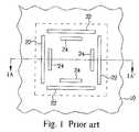
- FIG. 1shows a top view of a prior-art overlay vernier pattern for measuring layer-to-layer overlay alignment accuracy.
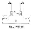
- FIG. 2shows a prior-art schematic cross-sectional view along line 1 A- 1 A′′ of the top view in FIG. 1.
- a typical Bar-in-Bar overlay vernier pattern 20is shown, for example by forming a plurality of alignment marks 22 in a material layer 10 and a plurality of alignment marks 24 in another material layer 12 over the material layer 10 , as depicted in the cross section in FIG. 2.
- the alignment marks 22 and 24are formed in a scribe line of a test wafer and are symmetric to a center of the overlay vernier pattern 20 .
- the material layer 10can be a silicon substrate, a conductive layer or an insulating layer.
- the material layer 12can be a conductive layer or an insulating layer.
- the alignment marks 22 and 24are formed by positive photoresist or negative photoresist, having a pattern such as a recess buried in the material layers 22 and 24 or as a column protruded from an underlying material layer.
- the alignment marks 22are after-etch-inspection (AEI) trench structures formed by methods known by those versed in the art.
- the alignment marks 24are after-development-inspection (ADI) photoresist column patterns.
- a distance B 1 between a midpoint of an alignment mark 24 and a midpoint of an alignment mark 22 adjacent to the alignment mark 24is measured using an alignment accuracy measurement tool, such as a scanning electron microscope.
- a distance B 2 between a midpoint of another alignment mark 24 and a midpoint of an alignment mark 22 adjacent to this alignment mark 24is also measured using the same alignment accuracy measurement tool.
- a difference between the distances B 1 and B 2is calculated, so as to get an alignment offset between the material layers 10 and 12 .
- another overlay vernier patternwhich includes a plurality of alignment marks in the material layer 12 and in the material layer over the material layer 12 , is formed in another region of the scribe line.
- the overlay vernier pattern for measuring multi-layer overlay alignment accuracycomprising: a plurality of first alignment marks positioned in a first material layer; a plurality of second alignment marks positioned in a second material layer over the first material layer; and a plurality of third alignment marks positioned in a third material layer over the second material layer; wherein a distance between a first alignment mark and a third alignment mark is a measure of misalignment of the first material layer to the third material layer, and a distance between the third alignment mark and a second alignment mark is a measure of misalignment of the third material layer to the second material layer.
- FIG. 1shows a top view of a prior-art overlay vernier pattern for measuring layer-to-layer overlay alignment accuracy.
- FIG. 2shows a prior-art schematic cross-sectional view along line 1 A- 1 A′′ of the top view in FIG. 1.
- FIG. 3shows a top view of an overlay vernier pattern for measuring multi-layer overlay alignment accuracy according to a first embodiment of the present invention.
- FIG. 4shows a cross-sectional view of an overlay vernier pattern along line 2 A- 2 A′′ of the top view in FIG. 3.
- FIG. 5shows a top view of an overlay vernier pattern for measuring multi-layer overlay alignment accuracy according to a second embodiment of the present invention.
- FIG. 6shows a cross-sectional view of an overlay vernier pattern along line 3 A- 3 A′′ of the top view in FIG. 5.
- FIG. 7shows a top view of an overlay vernier pattern for measuring multi-layer overlay alignment accuracy according to a third embodiment of the present invention.
- FIG. 8shows a cross-sectional view of an overlay vernier pattern along line 4 A- 4 A′′ of the top view in FIG. 7.
- FIG. 9shows a top view of an overlay vernier pattern for measuring multi-layer overlay alignment accuracy according to a fourth embodiment of the present invention.
- FIG. 10shows a cross-sectional view of an overlay vernier pattern along line 5 A- 5 A′′ of the top view in FIG. 9.
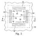
- FIG. 3shows a top view of an overlay vernier pattern for measuring multi-layer overlay alignment accuracy according to a first embodiment of the present invention.
- FIG. 4shows a cross-sectional view of the overlay vernier pattern along line 2 A- 2 A′′ of the top view in FIG. 3.
- a typical Bar-in-Bar overlay vernier pattern 40is shown, for example by forming a plurality of alignment marks 42 in a material layer 30 , a plurality of alignment marks 44 in a material layer 32 over the material layer 30 , and a plurality of alignment marks 46 in a material layer 34 over the material layer 32 , as depicted in the cross section in FIG. 4.
- a Box-in-Box overlay vernier pattern 40is susceptible in the present invention.
- the alignment marks 42 , 44 and 46are formed in a scribe line of a test wafer and are symmetric to a center of the overlay vernier pattern 40 .
- the material layer 30can be a silicon substrate, a conductive layer or an insulating layer.
- the material layers 32 and 34can be a conductive layer, such as a polysilicon layer.
- the alignment marks 42 , 44 , 46are formed by positive photoresist or negative photoresist, having a pattern such as a recess buried in the material layers 30 , 32 and 34 , or as a column protruded from an underlying material layer.
- the alignment marks 42 and 44are AEI trench structures formed by methods known by those versed in the art.
- the alignment marks 46are ADI photoresist column patterns.
- a meansconsisting of an algorithm stored in a permanent memory is provided to measure a distance C 1 between a midpoint of an alignment mark 42 and a midpoint of an alignment mark 44 adjacent to the alignment mark 42 .
- a distance C 2 between a midpoint of another alignment mark 42 and a midpoint of an alignment mark 44 adjacent to this alignment mark 42is also measured.
- the distances C 1 and C 2are compared to each other, and a difference between the distances C 1 and C 2 is calculated, so as to get an alignment offset between the material layers 30 and 32 .
- the same algorithm stored in the permanent memoryis provided to measure a distance D 1 between a midpoint of an alignment mark 44 and a midpoint of an alignment mark 46 adjacent to the alignment mark 44 .
- a distance D 2 between a midpoint of another alignment mark 44 and a midpoint of an alignment mark 46 adjacent to this alignment mark 44is also measured.
- the distances D 1 and D 2are compared to each other, and a difference between the distances D 1 and D 2 is calculated, so as to get an alignment offset between the material layers 32 and 34 .
- the alignment verniers for measuring the alignment accuracy between the material layer 30 and 32can be formed in the same region of the scribe line.
- the alignment marks 44can be repeatedly used when measuring the alignment accuracy between the material layers 30 and 32 , and measuring the alignment accuracy between the material layers 32 and 34 . Therefore, problems as waste of scribe line area and measuring time as happened in the prior art are effectively prevented in the present invention.
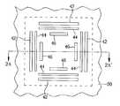
- FIG. 5 and FIG. 6A second embodiment of an overlay vernier pattern of the present invention is illustrated in FIG. 5 and FIG. 6.
- a three-layer overlay vernier pattern 60is shown.
- the overlay vernier pattern 60includes a plurality of alignment marks 62 in a material layer 50 , a plurality of alignment marks 64 in a material layer 52 over the material layer 50 , and a plurality of alignment marks 66 in a material layer 54 over the material layer 52 .
- the overlay vernier pattern 60is similar to the overlay vernier pattern 40 of the first embodiment, except the alignment marks 66 in the top material layer 54 are recesses etched in the material layer 54 .
- a distance E 1 between a midpoint of an alignment mark 62 and a midpoint of an alignment mark 64 adjacent to the alignment mark 62is measured.
- a distance E 2 between a midpoint of another alignment mark 62 and a midpoint of an alignment mark 64 adjacent to this alignment mark 62is also measured.
- the distances E 1 and E 2are compared to each other, and a difference between the distances E 1 and E 2 is calculated, so as to get an alignment offset between the material layers 50 and 52 .
- a distance F 1 between a midpoint of an alignment mark 64 and a midpoint of an alignment mark 66 adjacent to the alignment mark 64is measured.
- a distance F 2 between a midpoint of another alignment mark 64 and a midpoint of an alignment mark 66 adjacent to this alignment mark 64is also measured.
- the distances F 1 and F 2are compared to each other, and a difference between the distances F 1 and F 2 is calculated, so as to get an alignment offset between the material layers 52 and 54 .
- FIG. 7 and FIG. 8A third embodiment of an overlay vernier pattern of the present invention is illustrated in FIG. 7 and FIG. 8.
- the overlay vernier pattern 80includes a plurality of alignment marks 82 in a material layer 70 and a plurality of alignment marks 84 and 86 in a material layer 72 over the material layer 70 .
- the alignment marks 82 , 84 and 86are formed in a scribe line of a test wafer and are symmetric to a center of the overlay vernier pattern 80 .
- the material layer 70can be a conductive layer, such as a polysilicon layer or a silicon substrate. Alternatively, the material layer 70 can be an insulating layer.
- the material layer 72can be a developed photoresist layer.
- the alignment marks 82 , 84 , 86are formed by positive photoresist or negative photoresist, having a pattern such as a recess buried in the material layers 70 and 72 , or as a column protruded from an underlying material layer.
- the alignment marks 82are AEI trench structures formed by methods known by those versed in the art.
- the alignment marks 84are ADI photoresist trench structures formed by a first photolithographic process.
- the alignment marks 86are ADI photoresist trench structures formed by a second photolithographic process.
- a meansconsisting of an algorithm stored in a permanent memory is provided to measure a distance H 1 between a midpoint of an alignment mark 82 and a midpoint of an alignment mark 84 adjacent to the alignment mark 82 .
- a distance H 2 between a midpoint of another alignment mark 82 and a midpoint of an alignment mark 84 adjacent to this alignment mark 82is also measured.
- the distances H 1 and H 2are compared to each other, and a difference between the distances H 1 and H 2 is calculated, so as to get an alignment offset between the material layers 70 and 72 .
- the same algorithm stored in the permanent memoryis provided to measure a distance G 1 between a midpoint of an alignment mark 82 and a midpoint of an alignment mark 86 adjacent to the alignment mark 82 .
- a distance G 2 between a midpoint of another alignment mark 82 and a midpoint of an alignment mark 86 adjacent to this alignment mark 82is also measured.
- the distances G 1 and G 2are compared to each other, and a difference between the distances G 1 and G 2 is calculated, so as to get an alignment offset between the material layers 70 and 72 .
- the overlay vernier pattern 80also provides a measure of misalignment between the alignment marks 84 formed by the first photolithographic process and the alignment marks 86 formed by the second photolithographic process.
- a distance I 1 between a midpoint of an alignment mark 84 and a midpoint of an alignment mark 86 adjacent to the alignment mark 84is measured.
- a distance I 2 between a midpoint of another alignment mark 84 and a midpoint of an alignment mark 86 adjacent to this alignment mark 84is also measured.
- the distances I 1 and I 2are compared to each other, and a difference between the distances I 1 and I 2 is calculated, so as to get an alignment offset between the alignment marks 84 and 86 .
- the alignment verniers for measuring the alignment accuracy between the material layer 70 and the material layer 72 after the first photolithographic process is performed, the alignment verniers for measuring the alignment accuracy between the material layer 70 and the material layer 72 after the second photolithographic process is performed, and the alignment verniers for measuring the alignment accuracy of the first photolithographic process and the second photolithographic processcan be formed in the same region of the scribe line.
- the alignment marks 84 and 86can be repeatedly used when measuring the alignment accuracy between the material layers 70 and 72 , and measuring the alignment accuracy of the two photolithographic processes. Therefore, problems as waste of scribe line area and measuring time as happened in the prior art are effectively prevented in the present invention.
- FIG. 9 and FIG. 10A fourth embodiment of an overlay vernier pattern of the present invention is illustrated in FIG. 9 and FIG. 10.
- the overlay vernier pattern 100includes a plurality of alignment marks 102 in a material layer 90 , a plurality of alignment marks 104 in a material layer 92 over the material layer 50 , and a plurality of alignment marks 106 and 108 in a material layer 94 over the material layer 92 .
- the material layer 90is similar to the material layer 70 to be a conductive layer or an insulating layer
- the material layer 94is similar to the material layer 72 to be a developed photoresist layer.
- a difference between the overlay vernier pattern 80 and 100is that the material layer 92 is inserted between the material layers 90 and 94 .
- the material layer 92can be either a conductive layer or an insulating layer.
- the alignment marks 102 and 104are AEI trench structures formed by methods known by those versed in the art.
- the alignment marks 106are ADI photoresist trench structures formed by a first photolithographic process.
- the alignment marks 108are ADI photoresist trench structures formed by a second photolithographic process.
- a distance J between a midpoint of an alignment mark 102 and a midpoint of an alignment mark 106 adjacent to the alignment mark 102is measured.
- a distance J between a midpoint of 2 another alignment mark 102 and a midpoint of an alignment mark 106 adjacent to this alignment mark 102is also measured.
- the distances J 1 and J 2are compared to each other, and a difference between the distances J 1 and J 2 is calculated, so as to get an alignment offset between the material layers 90 and 94 .
- a distance J 1 ′′ between a midpoint of an alignment mark 102 and a midpoint of an alignment mark 108 adjacent to the alignment mark 102is measured.
- a distance J 2 ′′ between a midpoint of another alignment mark 102 and a midpoint of an alignment mark 108 adjacent to this alignment mark 102is also measured.
- the distances J 1 ′′ and J 2 ′′are compared to each other, and a difference between the distances J 1 ′′ and J 2 ′′ is calculated, so as to get an alignment offset between the material layers 90 and 94 .
- K 1 and K 2are measured to get an alignment offset between the material layers 92 and 94 after the first photolithographic process is performed.
- K 1 ′′ and K 2 ′′are measured to get an alignment offset between the material layers 92 and 94 after the second photolithographic process is performed.
- L 1 and L 2are measured to get an alignment offset between the alignment marks 106 formed by the first photolithographic process and the alignment marks 108 formed by the second photolithographic process.
- the present inventionforms alignment marks in each of the material layers in a region of the substrate. Therefore, layer-to-layer alignment accuracy measurement for any two of the material layers of the multi-layer structure can be simultaneously performed in the same region, so as to save a scribe line area and measuring time to increase the production throughput.
Landscapes
- Physics & Mathematics (AREA)
- General Physics & Mathematics (AREA)
- Exposure Of Semiconductors, Excluding Electron Or Ion Beam Exposure (AREA)
- Exposure And Positioning Against Photoresist Photosensitive Materials (AREA)
Abstract
Description
- 1. Field of the Invention[0001]
- The present invention relates to an overlay vernier pattern and a method for measuring multi-layer overlay alignment accuracy on a substrate, and more particularly, to an overlay vernier pattern and a method that measures overlay alignment of a photoresist layer with a plurality of material layers.[0002]
- 2. Description of the Prior Art[0003]
- Semiconductor integrated circuits undergo a variety of processing steps during manufacture, such as masking, resist coating, etching, and deposition. In many of these steps, material is overlaid or removed from the existing layer at specific locations in order to form the desired elements of the integrated circuit. Proper alignment of the various process layers is therefore critical.[0004]
- Registration is typically used to measure layer-to-layer alignment accuracy for a semiconductor process. Registration involves comparing a position of a subsequent layer to a position of an existing layer by overlaying a distinct pattern on a matching pattern that is previously formed on the existing layer. At least an alignment mark is formed in the distinct pattern and the matching pattern. A distance between the alignment mark in the subsequent layer and the alignment mark in the existing layer provides a measure of misalignment between these two layers. Currently available registration structures include Box-in-Box visual verniers and Bar-in-Bar visual verniers to determine the extent of registration, i.e., the amount of alignment offset.[0005]
- Please refer to FIG. 1, which shows a top view of a prior-art overlay vernier pattern for measuring layer-to-layer overlay alignment accuracy. FIG. 2 shows a prior-art schematic cross-sectional view along line[0006]1A-1A″ of the top view in FIG. 1. In FIG. 1, a typical Bar-in-Bar overlay vernier pattern20 is shown, for example by forming a plurality of
alignment marks 22 in amaterial layer 10 and a plurality ofalignment marks 24 inanother material layer 12 over thematerial layer 10, as depicted in the cross section in FIG. 2. Thealignment marks material layer 10 can be a silicon substrate, a conductive layer or an insulating layer. Thematerial layer 12 can be a conductive layer or an insulating layer. Thealignment marks material layers alignment marks 22 are after-etch-inspection (AEI) trench structures formed by methods known by those versed in the art. Thealignment marks 24 are after-development-inspection (ADI) photoresist column patterns. - When measuring misalignment of the[0007]
material layer 12 to thematerial layer 10, a distance B1between a midpoint of analignment mark 24 and a midpoint of analignment mark 22 adjacent to thealignment mark 24 is measured using an alignment accuracy measurement tool, such as a scanning electron microscope. In addition, a distance B2between a midpoint of anotheralignment mark 24 and a midpoint of analignment mark 22 adjacent to thisalignment mark 24 is also measured using the same alignment accuracy measurement tool. Following this, a difference between the distances B1and B2is calculated, so as to get an alignment offset between thematerial layers material layer 12 and a material layer (not shown) over thematerial layer 12, another overlay vernier pattern, which includes a plurality of alignment marks in thematerial layer 12 and in the material layer over thematerial layer 12, is formed in another region of the scribe line. - However, with the shrinking dimensions of modern integrated circuits, multi-layer structure is developed for a chip. For a three-layer structure or a more complicated structure, layer-to-layer alignment accuracy measurement is performed, respectively, for any two of the layers to occupy a scribe line area and waste measuring time. Therefore, development of an overlay vernier pattern and a measurement method to effectively measure the overlay alignment accuracy of the multi-layer structure has become important.[0008]
- It is an objective of the claimed invention to provide an overlay vernier pattern and a measurement method to effectively measure overlay alignment accuracy of a multilayer semiconductor structure, so as to improve the production throughput.[0009]
- According to the claimed invention, the overlay vernier pattern for measuring multi-layer overlay alignment accuracy comprising: a plurality of first alignment marks positioned in a first material layer; a plurality of second alignment marks positioned in a second material layer over the first material layer; and a plurality of third alignment marks positioned in a third material layer over the second material layer; wherein a distance between a first alignment mark and a third alignment mark is a measure of misalignment of the first material layer to the third material layer, and a distance between the third alignment mark and a second alignment mark is a measure of misalignment of the third material layer to the second material layer.[0010]
- It is an advantage of the present invention that alignment marks in each of the material layers in a three-layer structure or a more complicated structure are overlaid in a region of the substrate. Therefore, layer-to-layer alignment accuracy measurement for any two of the material layers can be simultaneously performed in the same region, so as to save a scribe line area and measuring time to increase the throughput of the semiconductor devices.[0011]
- These and other objectives of the claimed invention will no doubt become obvious to those of ordinary skill in the art after reading the following detailed description of the preferred embodiment that is illustrated in the various figures and drawings.[0012]
- FIG. 1 shows a top view of a prior-art overlay vernier pattern for measuring layer-to-layer overlay alignment accuracy.[0013]
- FIG. 2 shows a prior-art schematic cross-sectional view along line[0014]1A-1A″ of the top view in FIG. 1.
- FIG. 3 shows a top view of an overlay vernier pattern for measuring multi-layer overlay alignment accuracy according to a first embodiment of the present invention.[0015]
- FIG. 4 shows a cross-sectional view of an overlay vernier pattern along[0016]
line 2A-2A″ of the top view in FIG. 3. - FIG. 5 shows a top view of an overlay vernier pattern for measuring multi-layer overlay alignment accuracy according to a second embodiment of the present invention.[0017]
- FIG. 6 shows a cross-sectional view of an overlay vernier pattern along[0018]
line 3A-3A″ of the top view in FIG. 5. - FIG. 7 shows a top view of an overlay vernier pattern for measuring multi-layer overlay alignment accuracy according to a third embodiment of the present invention.[0019]
- FIG. 8 shows a cross-sectional view of an overlay vernier pattern along[0020]
line 4A-4A″ of the top view in FIG. 7. - FIG. 9 shows a top view of an overlay vernier pattern for measuring multi-layer overlay alignment accuracy according to a fourth embodiment of the present invention.[0021]
- FIG. 10 shows a cross-sectional view of an overlay vernier pattern along[0022]
line 5A-5A″ of the top view in FIG. 9. - Please refer to FIG. 3 and FIG. 4. FIG. 3 shows a top view of an overlay vernier pattern for measuring multi-layer overlay alignment accuracy according to a first embodiment of the present invention. FIG. 4 shows a cross-sectional view of the overlay vernier pattern along[0023]
line 2A-2A″ of the top view in FIG. 3. In FIG. 3, a typical Bar-in-Bar overlay vernier pattern40 is shown, for example by forming a plurality ofalignment marks 42 in amaterial layer 30, a plurality ofalignment marks 44 in amaterial layer 32 over thematerial layer 30, and a plurality ofalignment marks 46 in amaterial layer 34 over thematerial layer 32, as depicted in the cross section in FIG. 4. Alternatively, a Box-in-Box overlay vernier pattern40 is susceptible in the present invention. Thealignment marks material layer 30 can be a silicon substrate, a conductive layer or an insulating layer. Thematerial layers alignment marks material layers alignment marks alignment marks 46 are ADI photoresist column patterns. - When measuring misalignment of the[0024]
material layer 32 to thematerial layer 30, a means consisting of an algorithm stored in a permanent memory is provided to measure a distance C1between a midpoint of analignment mark 42 and a midpoint of analignment mark 44 adjacent to thealignment mark 42. A distance C2between a midpoint of anotheralignment mark 42 and a midpoint of analignment mark 44 adjacent to thisalignment mark 42 is also measured. Following this, the distances C1and C2are compared to each other, and a difference between the distances C1and C2is calculated, so as to get an alignment offset between thematerial layers - Similarly, when measuring misalignment of the[0025]
material layer 32 to thematerial layer 34, the same algorithm stored in the permanent memory is provided to measure a distance D1between a midpoint of analignment mark 44 and a midpoint of analignment mark 46 adjacent to thealignment mark 44. A distance D2between a midpoint of anotheralignment mark 44 and a midpoint of analignment mark 46 adjacent to thisalignment mark 44 is also measured. Following this, the distances D1and D2are compared to each other, and a difference between the distances D1and D2is calculated, so as to get an alignment offset between thematerial layers - According to the present invention, the alignment verniers for measuring the alignment accuracy between the[0026]
material layer material layer material layers material layers - A second embodiment of an overlay vernier pattern of the present invention is illustrated in FIG. 5 and FIG. 6. In the second embodiment, a three-layer overlay vernier pattern[0027]60 is shown. The overlay vernier pattern60 includes a plurality of alignment marks62 in a
material layer 50, a plurality of alignment marks64 in amaterial layer 52 over thematerial layer 50, and a plurality of alignment marks66 in amaterial layer 54 over thematerial layer 52. The overlay vernier pattern60 is similar to the overlay vernier pattern40 of the first embodiment, except the alignment marks66 in thetop material layer 54 are recesses etched in thematerial layer 54. - When measuring alignment accuracy of the overlay vernier pattern[0028]60, a distance E1between a midpoint of an
alignment mark 62 and a midpoint of analignment mark 64 adjacent to thealignment mark 62 is measured. A distance E2between a midpoint of anotheralignment mark 62 and a midpoint of analignment mark 64 adjacent to thisalignment mark 62 is also measured. Following this, the distances E1and E2are compared to each other, and a difference between the distances E1and E2is calculated, so as to get an alignment offset between thematerial layers - Similarly, when measuring misalignment of the[0029]
material layer 52 to thematerial layer 54, a distance F1between a midpoint of analignment mark 64 and a midpoint of analignment mark 66 adjacent to thealignment mark 64 is measured. A distance F2between a midpoint of anotheralignment mark 64 and a midpoint of analignment mark 66 adjacent to thisalignment mark 64 is also measured. Following this, the distances F1and F2are compared to each other, and a difference between the distances F1and F2is calculated, so as to get an alignment offset between thematerial layers - A third embodiment of an overlay vernier pattern of the present invention is illustrated in FIG. 7 and FIG. 8. In the third embodiment, a two-layer overlay vernier pattern[0030]80 is shown. The overlay vernier pattern80 includes a plurality of alignment marks82 in a
material layer 70 and a plurality of alignment marks84 and86 in amaterial layer 72 over thematerial layer 70. The alignment marks82,84 and86 are formed in a scribe line of a test wafer and are symmetric to a center of the overlay vernier pattern80. Thematerial layer 70 can be a conductive layer, such as a polysilicon layer or a silicon substrate. Alternatively, thematerial layer 70 can be an insulating layer. Thematerial layer 72 can be a developed photoresist layer. The alignment marks82,84,86 are formed by positive photoresist or negative photoresist, having a pattern such as a recess buried in the material layers70 and72, or as a column protruded from an underlying material layer. Ideally, the alignment marks82 are AEI trench structures formed by methods known by those versed in the art. The alignment marks84 are ADI photoresist trench structures formed by a first photolithographic process. The alignment marks86 are ADI photoresist trench structures formed by a second photolithographic process. - When measuring misalignment of the[0031]
material layer 70 to thematerial layer 72 after the first photolithographic process is performed, a means consisting of an algorithm stored in a permanent memory is provided to measure a distance H1between a midpoint of analignment mark 82 and a midpoint of analignment mark 84 adjacent to thealignment mark 82. A distance H2between a midpoint of anotheralignment mark 82 and a midpoint of analignment mark 84 adjacent to thisalignment mark 82 is also measured. Following this, the distances H1and H2are compared to each other, and a difference between the distances H1and H2is calculated, so as to get an alignment offset between thematerial layers - Similarly, when measuring misalignment of the[0032]
material layer 70 to thematerial layer 72 after the second photolithographic process is performed, the same algorithm stored in the permanent memory is provided to measure a distance G1between a midpoint of analignment mark 82 and a midpoint of analignment mark 86 adjacent to thealignment mark 82. A distance G2between a midpoint of anotheralignment mark 82 and a midpoint of analignment mark 86 adjacent to thisalignment mark 82 is also measured. Following this, the distances G1and G2are compared to each other, and a difference between the distances G1and G2is calculated, so as to get an alignment offset between thematerial layers - In addition, the overlay vernier pattern[0033]80 also provides a measure of misalignment between the alignment marks84 formed by the first photolithographic process and the alignment marks86 formed by the second photolithographic process.
- When measuring misalignment of the alignment marks[0034]84 to the alignment marks86, a distance I1between a midpoint of an
alignment mark 84 and a midpoint of analignment mark 86 adjacent to thealignment mark 84 is measured. A distance I2between a midpoint of anotheralignment mark 84 and a midpoint of analignment mark 86 adjacent to thisalignment mark 84 is also measured. Following this, the distances I1and I2are compared to each other, and a difference between the distances I1and I2is calculated, so as to get an alignment offset between the alignment marks84 and86. - According to the present invention, the alignment verniers for measuring the alignment accuracy between the[0035]
material layer 70 and thematerial layer 72 after the first photolithographic process is performed, the alignment verniers for measuring the alignment accuracy between thematerial layer 70 and thematerial layer 72 after the second photolithographic process is performed, and the alignment verniers for measuring the alignment accuracy of the first photolithographic process and the second photolithographic process, can be formed in the same region of the scribe line. Specifically, the alignment marks84 and86 can be repeatedly used when measuring the alignment accuracy between thematerial layers - A fourth embodiment of an overlay vernier pattern of the present invention is illustrated in FIG. 9 and FIG. 10. In the fourth embodiment, a three-layer overlay vernier pattern[0036]100 is shown. The overlay vernier pattern100 includes a plurality of alignment marks102 in a
material layer 90, a plurality of alignment marks104 in amaterial layer 92 over thematerial layer 50, and a plurality of alignment marks106 and108 in amaterial layer 94 over thematerial layer 92. Thematerial layer 90 is similar to thematerial layer 70 to be a conductive layer or an insulating layer, and thematerial layer 94 is similar to thematerial layer 72 to be a developed photoresist layer. A difference between the overlay vernier pattern80 and100 is that thematerial layer 92 is inserted between thematerial layers material layer 92 can be either a conductive layer or an insulating layer. - Ideally, the alignment marks[0037]102 and104 are AEI trench structures formed by methods known by those versed in the art. The alignment marks106 are ADI photoresist trench structures formed by a first photolithographic process. The alignment marks108 are ADI photoresist trench structures formed by a second photolithographic process.
- When measuring misalignment of the[0038]
material layer 90 to thematerial layer 94 after the first photolithographic process is performed, a distance J between a midpoint of analignment mark 102 and a midpoint of analignment mark 106 adjacent to thealignment mark 102 is measured. A distance J between a midpoint of2 anotheralignment mark 102 and a midpoint of analignment mark 106 adjacent to thisalignment mark 102 is also measured. Following this, the distances J1and J2are compared to each other, and a difference between the distances J1and J2is calculated, so as to get an alignment offset between thematerial layers - Similarly, when measuring misalignment of the[0039]
material layer 90 to thematerial layer 94 after the second photolithographic process is performed, a distance J1″ between a midpoint of analignment mark 102 and a midpoint of analignment mark 108 adjacent to thealignment mark 102 is measured. A distance J2″ between a midpoint of anotheralignment mark 102 and a midpoint of analignment mark 108 adjacent to thisalignment mark 102 is also measured. Following this, the distances J1″ and J2″ are compared to each other, and a difference between the distances J1″ and J2″ is calculated, so as to get an alignment offset between thematerial layers - K[0040]1and K2are measured to get an alignment offset between the
material layers material layers - In contrast to the prior art, the present invention forms alignment marks in each of the material layers in a region of the substrate. Therefore, layer-to-layer alignment accuracy measurement for any two of the material layers of the multi-layer structure can be simultaneously performed in the same region, so as to save a scribe line area and measuring time to increase the production throughput.[0041]
- Those skilled in the art will readily observe that numerous modifications and alterations of the device may be made while retaining the teachings of the invention. Accordingly, the above disclosure should be construed as limited only by the metes and bounds of the appended claims.[0042]
Claims (26)
1. An overlay vernier pattern for measuring multi-layer overlay alignment accuracy, the overlay vernier pattern comprising:
a plurality of first alignment marks positioned in a first material layer;
a plurality of second alignment marks positioned in a second material layer over the first material layer; and
a plurality of third alignment marks positioned in a third material layer over the second material layer;
wherein a distance between a first alignment mark and a third alignment mark is a measure of misalignment of the first material layer to the third material layer, and a distance between the third alignment mark and a second alignment mark is a measure of misalignment of the third material layer to the second material layer.
2. The overlay vernier pattern ofclaim 1 wherein the distance between a first alignment mark and a third alignment mark refers to a distance ranging from a midpoint of the first alignment mark to a midpoint of the third alignment mark.
3. The overlay vernier pattern ofclaim 1 wherein the distance between the third alignment mark and a second alignment mark refers to a distance ranging from a midpoint of the third alignment mark to a midpoint of the second alignment mark.
4. The overlay vernier pattern ofclaim 1 wherein when measuring misalignment between the first material layer and the third material layer, the distance between a first alignment mark and a third alignment mark is compared with another distance between an adjacent first alignment mark and an adjacent third alignment mark, and a difference between these two distances refers to an offset value for aligning the first material layer to the third material layer.
5. The overlay vernier pattern ofclaim 1 wherein when measuring misalignment between the third material layer and the second material layer, the distance between the third alignment mark and a second alignment mark is compared with another distance between an adjacent third alignment mark and an adjacent second alignment mark, and a difference between these two distances refers to an offset value for aligning the third material layer to the second material layer.
6. The overlay vernier pattern ofclaim 1 wherein a pattern of the first alignment marks and the second alignment marks is formed by positive photoresist.
7. The overlay vernier pattern ofclaim 1 wherein a pattern of the first alignment marks and the second alignment marks is formed by negative photoresist.
8. The overlay vernier pattern ofclaim 1 wherein the first material layer and the second material layer comprise polysilicon.
9. The overlay vernier pattern ofclaim 1 wherein the first material layer is a semiconductor substrate.
10. The overlay vernier pattern ofclaim 1 wherein the third material layer comprises a developed photoresist layer.
11. A method for measuring patterned multi-layer overlay alignment accuracy (AA) comprising:
providing a semiconductor substrate, the semiconductor substrate comprising a patterned first material layer, a patterned second material layer, and a patterned third material layer positioned on a surface of the semiconductor substrate, respectively, the first material layer comprising a plurality of first alignment marks, the second material layer comprising a plurality of second alignment marks, and the third material layer comprising a plurality of third alignment marks; and
providing a means consisting of an algorithm stored in permanent memory for measuring misalignment between a first alignment mark and a third alignment mark, and measuring misalignment between the third alignment mark and a second alignment mark.
12. The method ofclaim 11 wherein a method for measuring misalignment between the first alignment mark and the third alignment mark comprises measuring a distance between a midpoint of the first alignment mark and a midpoint of the third alignment mark, and comparing this distance with another distance between an adjacent first alignment mark and an adjacent third alignment mark, and a difference between these two distances refers to an offset value for aligning the first material layer to the third material layer.
13. The method ofclaim 11 wherein a method for measuring misalignment between the third alignment mark and the second alignment mark comprises measuring a distance between a midpoint of the third alignment mark and a midpoint of the second alignment mark, and comparing this distance with another distance between an adjacent third alignment mark and an adjacent second alignment mark, and a difference between these two distances refers to an offset value for aligning the third material layer to the second material layer.
14. The method of claim111 wherein a pattern of the first alignment marks and the second alignment marks is formed by positive photoresist.
15. The method of claim II wherein a pattern of the first alignment marks and the second alignment marks is formed by negative photoresist.
16. The method ofclaim 11 wherein the first material layer and the second material layer comprise polysilicon.
17. The method ofclaim 11 wherein the third material layer comprises a developed photoresist layer.
18. A method for measuring patterned multi-layer overlay alignment accuracy comprising:
providing a semiconductor substrate, the semiconductor substrate comprising at least a patterned material layer and a developed photoresist layer positioned on the patterned material layer, the material layer comprising a plurality of alignment marks and the photoresist layer comprising a plurality of first marks forming by a first photolithographic process and a plurality of second marks forming by a second photolithographic process; and
providing a means consisting of an algorithm stored in permanent memory for measuring misalignment between a first mark of the photoresist layer and a alignment mark in the material layer, and measuring misalignment between a second mark of the photoresist layer and the alignment mark in the material layer.
19. The method ofclaim 18 wherein a method for measuring misalignment between the first mark of the photoresist layer and the alignment mark in the material layer comprises measuring a distance between a midpoint of the first mark and a midpoint of the alignment mark, and comparing this distance with another distance between an adjacent first mark and an adjacent alignment mark, and a difference between these two distances refers to an offset value for aligning the material layer to photoresist layer after the first photolithographic process is performed.
20. The method ofclaim 18 wherein a method for measuring misalignment between the second mark of the photoresist layer and the alignment mark in the material layer comprises measuring a distance between a midpoint of the second mark and a midpoint of the alignment mark, and comparing this distance with another distance between an adjacent second mark and an adjacent alignment mark, and a difference between these two distances refers to an offset value for aligning the material layer to photoresist layer after the second photolithographic process is performed.
21. The method ofclaim 18 further comprises measuring a distance between a first mark and a second mark, and comparing this distance with another distance between an adjacent first mark and an adjacent second mark, and a difference between these two distances refers to an offset value for the first photolithographic process and the second photolithographic process.
22. The method ofclaim 18 wherein a pattern of the alignment marks is formed by positive photoresist.
23. The method ofclaim 18 wherein a pattern of the alignment marks is formed by negative photoresist.
24. The method ofclaim 18 wherein the material layer comprise polysilicon.
25. The method ofclaim 18 wherein the material layer comprise conductive layer.
26. The method ofclaim 18 wherein the material layer comprise insulating layer.
Priority Applications (3)
| Application Number | Priority Date | Filing Date | Title |
|---|---|---|---|
| US10/063,077US7190823B2 (en) | 2002-03-17 | 2002-03-17 | Overlay vernier pattern for measuring multi-layer overlay alignment accuracy and method for measuring the same |
| CNB031000835ACN1202559C (en) | 2002-03-17 | 2003-01-07 | Overlap vernier pattern and measurement method for measuring multi-layer overlay alignment accuracy |
| US11/162,028US7190824B2 (en) | 2002-03-17 | 2005-08-25 | Overlay vernier pattern for measuring multi-layer overlay alignment accuracy and method for measuring the same |
Applications Claiming Priority (1)
| Application Number | Priority Date | Filing Date | Title |
|---|---|---|---|
| US10/063,077US7190823B2 (en) | 2002-03-17 | 2002-03-17 | Overlay vernier pattern for measuring multi-layer overlay alignment accuracy and method for measuring the same |
Related Child Applications (1)
| Application Number | Title | Priority Date | Filing Date |
|---|---|---|---|
| US11/162,028DivisionUS7190824B2 (en) | 2002-03-17 | 2005-08-25 | Overlay vernier pattern for measuring multi-layer overlay alignment accuracy and method for measuring the same |
Publications (2)
| Publication Number | Publication Date |
|---|---|
| US20030174879A1true US20030174879A1 (en) | 2003-09-18 |
| US7190823B2 US7190823B2 (en) | 2007-03-13 |
Family
ID=28038684
Family Applications (2)
| Application Number | Title | Priority Date | Filing Date |
|---|---|---|---|
| US10/063,077Expired - LifetimeUS7190823B2 (en) | 2002-03-17 | 2002-03-17 | Overlay vernier pattern for measuring multi-layer overlay alignment accuracy and method for measuring the same |
| US11/162,028Expired - LifetimeUS7190824B2 (en) | 2002-03-17 | 2005-08-25 | Overlay vernier pattern for measuring multi-layer overlay alignment accuracy and method for measuring the same |
Family Applications After (1)
| Application Number | Title | Priority Date | Filing Date |
|---|---|---|---|
| US11/162,028Expired - LifetimeUS7190824B2 (en) | 2002-03-17 | 2005-08-25 | Overlay vernier pattern for measuring multi-layer overlay alignment accuracy and method for measuring the same |
Country Status (2)
| Country | Link |
|---|---|
| US (2) | US7190823B2 (en) |
| CN (1) | CN1202559C (en) |
Cited By (59)
| Publication number | Priority date | Publication date | Assignee | Title |
|---|---|---|---|---|
| US20030141606A1 (en)* | 2002-01-31 | 2003-07-31 | Hiroyuki Yusa | Resist pattern for alignment measurement |
| US20040092080A1 (en)* | 2002-11-08 | 2004-05-13 | Nanya Technology Corporation | Marks and method for multi-layer alignment |
| US20050094145A1 (en)* | 2003-11-05 | 2005-05-05 | Lin Yen Y. | Overlay mark for aligning different layers on a semiconductor wafer |
| US20050276465A1 (en)* | 2002-03-17 | 2005-12-15 | Tzu-Ching Chen | Overlay vernier pattern for measuring multi-layer overlay alignment accuracy and method for measuring the same |
| US20050286052A1 (en)* | 2004-06-23 | 2005-12-29 | Kevin Huggins | Elongated features for improved alignment process integration |
| US20060103034A1 (en)* | 2004-11-15 | 2006-05-18 | Kuo-Kuei Fu | Overlay mark for a non-critical layer of critical dimensions |
| US20060110070A1 (en)* | 2004-11-23 | 2006-05-25 | Picciotto Carl E | Multiple layer alignment sensing |
| US20060228816A1 (en)* | 2005-04-06 | 2006-10-12 | Taiwan Semiconductor Manufacturing Company, Ltd. | System and method for overlay measurement in semiconductor manufacturing |
| KR100650733B1 (en) | 2005-04-04 | 2006-11-27 | 주식회사 하이닉스반도체 | Measurement mark of semiconductor device |
| SG127790A1 (en)* | 2005-06-01 | 2006-12-29 | Mitsubishi Electric Corp | Inspection method, and manufacturing method for liquid crystal display using inspection method |
| US20070026543A1 (en)* | 2005-07-25 | 2007-02-01 | Takashi Sato | Method for forming misalignment inspection mark and method for manufacturing semiconductor device |
| US20070138388A1 (en)* | 2003-10-16 | 2007-06-21 | Ward Billy W | Ion sources, systems and methods |
| KR100739259B1 (en) | 2006-03-08 | 2007-07-12 | 주식회사 하이닉스반도체 | Nesting measurement vernier and its formation method |
| US20070158580A1 (en)* | 2003-10-16 | 2007-07-12 | Ward Billy W | Ion sources, systems and methods |
| US20070158581A1 (en)* | 2003-10-16 | 2007-07-12 | Ward Billy W | Ion sources, systems and methods |
| US20070158558A1 (en)* | 2003-10-16 | 2007-07-12 | Ward Billy W | Ion sources, systems and methods |
| US20070158556A1 (en)* | 2003-10-16 | 2007-07-12 | Ward Billy W | Ion sources, systems and methods |
| US20070158557A1 (en)* | 2003-10-16 | 2007-07-12 | Ward Billy W | Ion sources, systems and methods |
| US20070158582A1 (en)* | 2003-10-16 | 2007-07-12 | Ward Billy W | Ion sources, systems and methods |
| US20070187621A1 (en)* | 2003-10-16 | 2007-08-16 | Ward Billy W | Ion sources, systems and methods |
| US20070194226A1 (en)* | 2003-10-16 | 2007-08-23 | Ward Billy W | Ion sources, systems and methods |
| US20070194251A1 (en)* | 2003-10-16 | 2007-08-23 | Ward Billy W | Ion sources, systems and methods |
| WO2007067316A3 (en)* | 2005-12-02 | 2007-09-13 | Alis Corp | Ion sources, systems and methods |
| US20070210251A1 (en)* | 2003-10-16 | 2007-09-13 | Ward Billy W | Ion sources, systems and methods |
| US20070227883A1 (en)* | 2006-03-20 | 2007-10-04 | Ward Billy W | Systems and methods for a helium ion pump |
| US20070228287A1 (en)* | 2006-03-20 | 2007-10-04 | Alis Technology Corporation | Systems and methods for a gas field ionization source |
| US20070296935A1 (en)* | 2006-06-23 | 2007-12-27 | Joon-Sung Kim | Substrate having alignment marks and method of obtaining alignment information using the same |
| US20080003705A1 (en)* | 2006-06-28 | 2008-01-03 | Hynix Semiconductor Inc. | Overlay vernier key and method for fabricating the same |
| US7368727B2 (en) | 2003-10-16 | 2008-05-06 | Alis Technology Corporation | Atomic level ion source and method of manufacture and operation |
| US7504639B2 (en) | 2003-10-16 | 2009-03-17 | Alis Corporation | Ion sources, systems and methods |
| US7521693B2 (en) | 2003-10-16 | 2009-04-21 | Alis Corporation | Ion sources, systems and methods |
| US20090114840A1 (en)* | 2003-10-16 | 2009-05-07 | Ward Billy W | Ion sources, systems and methods |
| US7554096B2 (en) | 2003-10-16 | 2009-06-30 | Alis Corporation | Ion sources, systems and methods |
| US7557360B2 (en) | 2003-10-16 | 2009-07-07 | Alis Corporation | Ion sources, systems and methods |
| US7601953B2 (en) | 2006-03-20 | 2009-10-13 | Alis Corporation | Systems and methods for a gas field ion microscope |
| WO2009141720A1 (en)* | 2008-05-22 | 2009-11-26 | Micronic Laser Systems Ab | Method and apparatus for overlay compensation between subsequently patterned layers on workpiece |
| US7804068B2 (en) | 2006-11-15 | 2010-09-28 | Alis Corporation | Determining dopant information |
| US20110012271A1 (en)* | 2009-07-14 | 2011-01-20 | Chiu Chui-Fu | Integrated alignment and overlay mark |
| US8110814B2 (en) | 2003-10-16 | 2012-02-07 | Alis Corporation | Ion sources, systems and methods |
| JP2012124457A (en)* | 2010-12-09 | 2012-06-28 | Hynix Semiconductor Inc | Overlay vernier mask pattern, method of forming the same, semiconductor element containing overlay vernier pattern, and method of forming the same |
| US8288877B1 (en) | 2008-10-25 | 2012-10-16 | Hrl Laboratories, Llc | Actuator enhanced alignment of self-assembled microstructures |
| US20130017378A1 (en)* | 2009-05-29 | 2013-01-17 | Asml Netherlands B.V. | Apparatus and Method for Providing Resist Alignment Marks in a Double Patterning Lithographic Process |
| US8736082B1 (en)* | 2008-10-25 | 2014-05-27 | Hrl Laboratories, Llc | Key structure and expansion enhanced alignment of self-assembled microstructures |
| US20140285652A1 (en)* | 2013-03-22 | 2014-09-25 | Kabushiki Kaisha Toshiba | Method for measuring pattern misalignment |
| US20150009488A1 (en)* | 2013-07-08 | 2015-01-08 | Kabushiki Kaisha Toshiba | Mask distortion measuring apparatus and method of measuring mask distortion |
| US20150028500A1 (en)* | 2013-07-26 | 2015-01-29 | Globalfoundries Inc. | Forming alignment mark and resulting mark |
| US8970050B2 (en) | 2012-08-17 | 2015-03-03 | SK Hynix Inc. | Semiconductor memory device including alignment key structures |
| US9159527B2 (en) | 2003-10-16 | 2015-10-13 | Carl Zeiss Microscopy, Llc | Systems and methods for a gas field ionization source |
| KR101714616B1 (en) | 2016-05-30 | 2017-04-26 | (주)오로스 테크놀로지 | Method for measuring overlay between three layers |
| CN107305321A (en)* | 2016-04-21 | 2017-10-31 | 中芯国际集成电路制造(上海)有限公司 | A kind of method for examining lithography alignment accuracy |
| WO2018162316A1 (en) | 2017-03-09 | 2018-09-13 | Carl Zeiss Smt Gmbh | Method and apparatus for analyzing a defective location of a photolithographic mask |
| US10199330B2 (en) | 2013-12-23 | 2019-02-05 | Infineon Technologies Ag | Alignment mark arrangement, semiconductor workpiece, and method for aligning a wafer |
| US10461038B1 (en)* | 2018-08-31 | 2019-10-29 | Micron Technology, Inc. | Methods of alignment marking semiconductor wafers, and semiconductor packages having portions of alignment markings |
| US20200185335A1 (en)* | 2015-12-23 | 2020-06-11 | Infineon Technologies Austria Ag | Method of Manufacturing a Semiconductor Device with Epitaxial Layers and an Alignment Mark |
| CN112034677A (en)* | 2020-09-17 | 2020-12-04 | 合肥晶合集成电路有限公司 | Overlay mark, overlay mark method and overlay measuring method |
| US11037882B2 (en)* | 2012-06-28 | 2021-06-15 | Taiwan Semiconductor Manufacturing Company, Ltd. | Overlay mark |
| CN113109997A (en)* | 2021-03-18 | 2021-07-13 | 上海信及光子集成技术有限公司 | Method and structure for measuring photoetching overlay error before and after epitaxy |
| US11392044B2 (en) | 2016-12-23 | 2022-07-19 | Asml Netherlands B.V. | Method of determining a position of a feature |
| US20220320002A1 (en)* | 2021-04-02 | 2022-10-06 | Changxin Memory Technologies, Inc. | Structure for alignment measurement mark and method for alignment measurement |
Families Citing this family (53)
| Publication number | Priority date | Publication date | Assignee | Title |
|---|---|---|---|---|
| US20050244729A1 (en)* | 2004-04-29 | 2005-11-03 | United Microelectronics Corp. | Method of measuring the overlay accuracy of a multi-exposure process |
| KR100598988B1 (en)* | 2005-05-18 | 2006-07-12 | 주식회사 하이닉스반도체 | Overlay vernier and semiconductor device manufacturing method using the same |
| KR100689709B1 (en)* | 2005-08-10 | 2007-03-08 | 삼성전자주식회사 | Overlay Marks for Manufacturing Semiconductor Devices and Overlay Measurement Methods Using the Same |
| KR100715280B1 (en)* | 2005-10-01 | 2007-05-08 | 삼성전자주식회사 | How to measure overlay precision using overlay keys |
| US7952213B2 (en)* | 2006-03-29 | 2011-05-31 | Macronix International Co., Ltd. | Overlay mark arrangement for reducing overlay shift |
| US7449792B2 (en)* | 2006-04-25 | 2008-11-11 | Macronix International Co., Ltd. | Pattern registration mark designs for use in photolithography and methods of using the same |
| US7927960B2 (en)* | 2006-12-11 | 2011-04-19 | Macronix International Co., Ltd. | Method of improving overlay performance in semiconductor manufacture |
| US8609441B2 (en)* | 2006-12-12 | 2013-12-17 | Asml Netherlands B.V. | Substrate comprising a mark |
| US8722179B2 (en)* | 2006-12-12 | 2014-05-13 | Asml Netherlands B.V. | Substrate comprising a mark |
| KR100870316B1 (en)* | 2006-12-28 | 2008-11-25 | 주식회사 하이닉스반도체 | Overlay vernier of semiconductor device and manufacturing method thereof |
| US7599063B2 (en)* | 2007-03-29 | 2009-10-06 | Macronix International Co., Ltd. | Method for checking alignment accuracy using overlay mark |
| CN101398630B (en)* | 2007-09-25 | 2010-10-13 | 南亚科技股份有限公司 | Alignment and overlay mark, mask structure and using method thereof |
| US7948060B2 (en)* | 2008-07-01 | 2011-05-24 | Xmos Limited | Integrated circuit structure |
| US8786054B2 (en)* | 2009-11-16 | 2014-07-22 | Taiwan Semiconductor Manufacturing Company, Ltd. | Structure for integrated circuit alignment |
| US8329360B2 (en) | 2009-12-04 | 2012-12-11 | Taiwan Semiconductor Manufacturing Company, Ltd. | Method and apparatus of providing overlay |
| TWI470713B (en)* | 2010-07-08 | 2015-01-21 | United Microelectronics Corp | Semiconductor manufacturing process and monitoring method thereof |
| US9927718B2 (en)* | 2010-08-03 | 2018-03-27 | Kla-Tencor Corporation | Multi-layer overlay metrology target and complimentary overlay metrology measurement systems |
| CN102543954B (en)* | 2010-12-08 | 2016-05-04 | 无锡华润上华科技有限公司 | Overlay mark |
| CN102543956B (en)* | 2010-12-08 | 2016-07-06 | 无锡华润上华科技有限公司 | Multilayer overlay mark |
| CN102738121B (en)* | 2011-04-08 | 2016-06-08 | 中芯国际集成电路制造(上海)有限公司 | A kind of alignment deviation check mark and making method thereof |
| CN102809899A (en)* | 2011-05-31 | 2012-12-05 | 无锡华润上华半导体有限公司 | Position aligning parameter calculation method |
| CN102543684A (en)* | 2011-11-11 | 2012-07-04 | 上海华力微电子有限公司 | Graphic structure design integrated with measurement of line width and alignment precision |
| US8736084B2 (en)* | 2011-12-08 | 2014-05-27 | Taiwan Semiconductor Manufacturing Company, Ltd. | Structure and method for E-beam in-chip overlay mark |
| CN104576610A (en)* | 2013-10-10 | 2015-04-29 | 无锡华润上华科技有限公司 | Method for improving semiconductor metal overlay alignment measurement mark |
| US9054113B1 (en)* | 2013-12-30 | 2015-06-09 | Nanya Technology Corporation | Box-in-box overlay mark |
| CN104849525B (en)* | 2014-02-13 | 2017-12-01 | 上海和辉光电有限公司 | Use the method for testing of test suite |
| CN104952851B (en)* | 2014-03-28 | 2017-11-14 | 中芯国际集成电路制造(上海)有限公司 | Alignment mark and its alignment methods |
| CN104952846B (en)* | 2014-03-28 | 2018-07-20 | 中芯国际集成电路制造(上海)有限公司 | Overlay mark |
| KR102237698B1 (en)* | 2014-04-15 | 2021-04-08 | 삼성전자주식회사 | Method of detecting an asymmetric portion of an overlay mark and method of measuring an overlay including the same |
| CN105225978B (en)* | 2014-06-17 | 2019-06-04 | 联华电子股份有限公司 | Correction Method of Overlay Error |
| US9305884B1 (en) | 2014-09-26 | 2016-04-05 | United Microelectronics Corp. | Overlay mark and method for forming the same |
| EP3197807B1 (en)* | 2014-09-26 | 2019-12-11 | Hewlett-Packard Development Company, L.P. | Frame length adjustment |
| KR102421913B1 (en)* | 2014-12-29 | 2022-07-19 | 삼성디스플레이 주식회사 | Exposure method, exposure device for performing the method and manufacturing method of display substrate using the method |
| CN104698773B (en)* | 2015-03-31 | 2017-06-16 | 上海华力微电子有限公司 | Photoetching alignment mark structure and its manufacture method |
| CN106324996B (en)* | 2015-06-15 | 2017-10-20 | 中国科学院上海光学精密机械研究所 | Litho machine original position multi channel imaging quality detection device and method |
| WO2017009036A1 (en) | 2015-07-13 | 2017-01-19 | Asml Netherlands B.V. | Lithographic apparatus and device manufacturing method |
| NL2017120A (en)* | 2015-07-16 | 2017-01-17 | Asml Netherlands Bv | Lithographic apparatus and device manufacturing method |
| KR20170131802A (en)* | 2016-05-20 | 2017-11-30 | 삼성디스플레이 주식회사 | Display apparatus, method of driving the same and method of manufacturing the same |
| CN106323472B (en)* | 2016-08-24 | 2018-06-12 | 中国科学院西安光学精密机械研究所 | Spectrum restoration correction method based on polarization interferometer |
| CN106783672A (en)* | 2016-11-30 | 2017-05-31 | 武汉新芯集成电路制造有限公司 | A kind of standard film for verifying Overlay board precision, preparation method and verification method |
| CN106371294B (en)* | 2016-12-01 | 2018-10-26 | 京东方科技集团股份有限公司 | A kind of production method of display base plate, display base plate and display device |
| KR102401179B1 (en)* | 2017-12-12 | 2022-05-24 | 삼성전자주식회사 | Aperture system of electron beam apparatus, electron beam exposure apparatus, and electron beam exposure apparatus system |
| US10504851B2 (en) | 2018-02-26 | 2019-12-10 | Globalfoundries Inc. | Structure and method to improve overlay performance in semiconductor devices |
| CN108628107A (en)* | 2018-04-13 | 2018-10-09 | 上海华力集成电路制造有限公司 | Overlay error measurement method and overlay mark |
| CN108803264B (en)* | 2018-06-08 | 2020-06-16 | 上海华虹宏力半导体制造有限公司 | Method for centralized placement of multiple alignment marks on wafer and determination of lithography position |
| CN109411449B (en)* | 2018-11-21 | 2020-04-10 | 武汉新芯集成电路制造有限公司 | Wafer assembly and wafer alignment method |
| CN110676243B (en)* | 2019-09-30 | 2021-09-14 | 芯盟科技有限公司 | Chip and alignment method |
| CN113534626B (en)* | 2020-04-14 | 2024-07-16 | 中国科学院微电子研究所 | Marking system and measurement method for overlay accuracy measurement |
| CN113555345B (en)* | 2020-04-23 | 2024-02-06 | 长鑫存储技术有限公司 | Semiconductor mark and forming method thereof |
| CN111708254B (en)* | 2020-05-28 | 2021-06-01 | 长江存储科技有限责任公司 | Photoetching alignment method and system |
| CN112015061A (en)* | 2020-08-27 | 2020-12-01 | 上海华力集成电路制造有限公司 | Overlay precision measurement mark and use method thereof |
| CN113093479B (en)* | 2021-04-02 | 2022-10-28 | 长鑫存储技术有限公司 | Alignment measurement mark structure and alignment measurement method |
| CN118838119B (en)* | 2023-04-11 | 2025-09-19 | 长鑫存储技术有限公司 | Exposure compensation amount determining method |
Citations (24)
| Publication number | Priority date | Publication date | Assignee | Title |
|---|---|---|---|---|
| US5005046A (en)* | 1989-03-20 | 1991-04-02 | Fujitsu Limited | Pattern forming method |
| US5322593A (en)* | 1991-11-21 | 1994-06-21 | Nec Corporation | Method for manufacturing polyimide multilayer wiring substrate |
| US5614767A (en)* | 1993-12-10 | 1997-03-25 | Nec Corporation | Alignment accuracy check pattern |
| US5635336A (en)* | 1993-10-15 | 1997-06-03 | Hyundai Electronics Industries Co., Ltd. | Method for the preparation of a pattern overlay accuracy-measuring mark |
| US5783340A (en)* | 1995-09-06 | 1998-07-21 | Sandia Corporation | Method for photolithographic definition of recessed features on a semiconductor wafer utilizing auto-focusing alignment |
| US5866447A (en)* | 1996-09-06 | 1999-02-02 | Holtek Microelectonics, Inc. | Modified zero layer align method of twin well MOS fabrication |
| US5912983A (en)* | 1997-01-24 | 1999-06-15 | Oki Electric Industry Co., Ltd | Overlay accuracy measuring method |
| US5917205A (en)* | 1995-06-01 | 1999-06-29 | Kabushiki Kaisha Toshiba | Photolithographic alignment marks based on circuit pattern feature |
| US6077756A (en)* | 1998-04-24 | 2000-06-20 | Vanguard International Semiconductor | Overlay target pattern and algorithm for layer-to-layer overlay metrology for semiconductor processing |
| US6118517A (en)* | 1996-08-29 | 2000-09-12 | Nec Corporation | Mask pattern for alignment |
| US6172409B1 (en)* | 1997-06-27 | 2001-01-09 | Cypress Semiconductor Corp. | Buffer grated structure for metrology mark and method for making the same |
| US6218200B1 (en)* | 2000-07-14 | 2001-04-17 | Motorola, Inc. | Multi-layer registration control for photolithography processes |
| US6228705B1 (en)* | 1999-02-03 | 2001-05-08 | International Business Machines Corporation | Overlay process for fabricating a semiconductor device |
| US6309944B1 (en)* | 2000-05-26 | 2001-10-30 | Taiwan Semiconductor Manufacturing Company | Overlay matching method which eliminates alignment induced errors and optimizes lens matching |
| US6319791B1 (en)* | 1998-10-27 | 2001-11-20 | Nec Corporation | Semiconductor device manufacturing method and semiconductor device |
| US6362491B1 (en)* | 1999-10-01 | 2002-03-26 | Taiwan Semiconductor Manufacturing Company | Method of overlay measurement in both X and Y directions for photo stitch process |
| US6448147B2 (en)* | 1998-03-27 | 2002-09-10 | Masahiro Komuro | Semiconductor device and method for manufacturing the same |
| US6716653B2 (en)* | 2000-02-25 | 2004-04-06 | Xilinx, Inc. | Mask alignment structure for IC layers |
| US6801313B1 (en)* | 1999-07-28 | 2004-10-05 | Nec Electronics Corporation | Overlay mark, method of measuring overlay accuracy, method of making alignment and semiconductor device therewith |
| US6849957B2 (en)* | 2000-05-30 | 2005-02-01 | Renesas Technology Corp. | Photomask including auxiliary mark area, semiconductor device and manufacturing method thereof |
| US6864589B2 (en)* | 2001-03-30 | 2005-03-08 | Sharp Laboratories Of America, Inc. | X/Y alignment vernier formed on a substrate |
| US6897956B2 (en)* | 2002-02-25 | 2005-05-24 | Hitachi, Ltd. | Apparatus and method for measuring alignment accuracy, as well as method and system for manufacturing semiconductor device |
| US20050276485A1 (en)* | 2004-06-10 | 2005-12-15 | Hitachi Software Engineering Co., Ltd. | Pattern recognition system utilizing an expression profile |
| US20050276465A1 (en)* | 2002-03-17 | 2005-12-15 | Tzu-Ching Chen | Overlay vernier pattern for measuring multi-layer overlay alignment accuracy and method for measuring the same |
Family Cites Families (3)
| Publication number | Priority date | Publication date | Assignee | Title |
|---|---|---|---|---|
| TW436878B (en)* | 1998-09-08 | 2001-05-28 | Mosel Vitelic Inc | Method for checking accuracy of a measuring instrument for overlay machine |
| US6077766A (en)* | 1999-06-25 | 2000-06-20 | International Business Machines Corporation | Variable thickness pads on a substrate surface |
| US6636313B2 (en)* | 2002-01-12 | 2003-10-21 | Taiwan Semiconductor Manufacturing Co. Ltd | Method of measuring photoresist and bump misalignment |
- 2002
- 2002-03-17USUS10/063,077patent/US7190823B2/ennot_activeExpired - Lifetime
- 2003
- 2003-01-07CNCNB031000835Apatent/CN1202559C/ennot_activeExpired - Lifetime
- 2005
- 2005-08-25USUS11/162,028patent/US7190824B2/ennot_activeExpired - Lifetime
Patent Citations (25)
| Publication number | Priority date | Publication date | Assignee | Title |
|---|---|---|---|---|
| US5005046A (en)* | 1989-03-20 | 1991-04-02 | Fujitsu Limited | Pattern forming method |
| US5322593A (en)* | 1991-11-21 | 1994-06-21 | Nec Corporation | Method for manufacturing polyimide multilayer wiring substrate |
| US5635336A (en)* | 1993-10-15 | 1997-06-03 | Hyundai Electronics Industries Co., Ltd. | Method for the preparation of a pattern overlay accuracy-measuring mark |
| US5614767A (en)* | 1993-12-10 | 1997-03-25 | Nec Corporation | Alignment accuracy check pattern |
| US5917205A (en)* | 1995-06-01 | 1999-06-29 | Kabushiki Kaisha Toshiba | Photolithographic alignment marks based on circuit pattern feature |
| US5783340A (en)* | 1995-09-06 | 1998-07-21 | Sandia Corporation | Method for photolithographic definition of recessed features on a semiconductor wafer utilizing auto-focusing alignment |
| US6118517A (en)* | 1996-08-29 | 2000-09-12 | Nec Corporation | Mask pattern for alignment |
| US5866447A (en)* | 1996-09-06 | 1999-02-02 | Holtek Microelectonics, Inc. | Modified zero layer align method of twin well MOS fabrication |
| US5912983A (en)* | 1997-01-24 | 1999-06-15 | Oki Electric Industry Co., Ltd | Overlay accuracy measuring method |
| US6172409B1 (en)* | 1997-06-27 | 2001-01-09 | Cypress Semiconductor Corp. | Buffer grated structure for metrology mark and method for making the same |
| US6448147B2 (en)* | 1998-03-27 | 2002-09-10 | Masahiro Komuro | Semiconductor device and method for manufacturing the same |
| US6077756A (en)* | 1998-04-24 | 2000-06-20 | Vanguard International Semiconductor | Overlay target pattern and algorithm for layer-to-layer overlay metrology for semiconductor processing |
| US6319791B1 (en)* | 1998-10-27 | 2001-11-20 | Nec Corporation | Semiconductor device manufacturing method and semiconductor device |
| US6228705B1 (en)* | 1999-02-03 | 2001-05-08 | International Business Machines Corporation | Overlay process for fabricating a semiconductor device |
| US6801313B1 (en)* | 1999-07-28 | 2004-10-05 | Nec Electronics Corporation | Overlay mark, method of measuring overlay accuracy, method of making alignment and semiconductor device therewith |
| US6362491B1 (en)* | 1999-10-01 | 2002-03-26 | Taiwan Semiconductor Manufacturing Company | Method of overlay measurement in both X and Y directions for photo stitch process |
| US6716653B2 (en)* | 2000-02-25 | 2004-04-06 | Xilinx, Inc. | Mask alignment structure for IC layers |
| US6309944B1 (en)* | 2000-05-26 | 2001-10-30 | Taiwan Semiconductor Manufacturing Company | Overlay matching method which eliminates alignment induced errors and optimizes lens matching |
| US6849957B2 (en)* | 2000-05-30 | 2005-02-01 | Renesas Technology Corp. | Photomask including auxiliary mark area, semiconductor device and manufacturing method thereof |
| US6218200B1 (en)* | 2000-07-14 | 2001-04-17 | Motorola, Inc. | Multi-layer registration control for photolithography processes |
| US6864589B2 (en)* | 2001-03-30 | 2005-03-08 | Sharp Laboratories Of America, Inc. | X/Y alignment vernier formed on a substrate |
| US7008756B2 (en)* | 2001-03-30 | 2006-03-07 | Sharp Laboratories Of America, Inc. | Method of fabricating an X/Y alignment vernier |
| US6897956B2 (en)* | 2002-02-25 | 2005-05-24 | Hitachi, Ltd. | Apparatus and method for measuring alignment accuracy, as well as method and system for manufacturing semiconductor device |
| US20050276465A1 (en)* | 2002-03-17 | 2005-12-15 | Tzu-Ching Chen | Overlay vernier pattern for measuring multi-layer overlay alignment accuracy and method for measuring the same |
| US20050276485A1 (en)* | 2004-06-10 | 2005-12-15 | Hitachi Software Engineering Co., Ltd. | Pattern recognition system utilizing an expression profile |
Cited By (102)
| Publication number | Priority date | Publication date | Assignee | Title |
|---|---|---|---|---|
| US20070004059A1 (en)* | 2002-01-31 | 2007-01-04 | Hiroyuki Yusa | Method of measuring alignment of measurement pattern |
| US7670922B2 (en)* | 2002-01-31 | 2010-03-02 | Oki Semiconductor Co., Ltd. | Method of measuring alignment of measurement pattern |
| US20030141606A1 (en)* | 2002-01-31 | 2003-07-31 | Hiroyuki Yusa | Resist pattern for alignment measurement |
| US20050276465A1 (en)* | 2002-03-17 | 2005-12-15 | Tzu-Ching Chen | Overlay vernier pattern for measuring multi-layer overlay alignment accuracy and method for measuring the same |
| US7190823B2 (en)* | 2002-03-17 | 2007-03-13 | United Microelectronics Corp. | Overlay vernier pattern for measuring multi-layer overlay alignment accuracy and method for measuring the same |
| US7190824B2 (en) | 2002-03-17 | 2007-03-13 | United Microelectronics Corp. | Overlay vernier pattern for measuring multi-layer overlay alignment accuracy and method for measuring the same |
| US20040092080A1 (en)* | 2002-11-08 | 2004-05-13 | Nanya Technology Corporation | Marks and method for multi-layer alignment |
| US6962854B2 (en)* | 2002-11-08 | 2005-11-08 | Nanya Technology Corporation | Marks and method for multi-layer alignment |
| US7557358B2 (en) | 2003-10-16 | 2009-07-07 | Alis Corporation | Ion sources, systems and methods |
| US7368727B2 (en) | 2003-10-16 | 2008-05-06 | Alis Technology Corporation | Atomic level ion source and method of manufacture and operation |
| US7786451B2 (en) | 2003-10-16 | 2010-08-31 | Alis Corporation | Ion sources, systems and methods |
| US20070210251A1 (en)* | 2003-10-16 | 2007-09-13 | Ward Billy W | Ion sources, systems and methods |
| US7495232B2 (en) | 2003-10-16 | 2009-02-24 | Alis Corporation | Ion sources, systems and methods |
| US8110814B2 (en) | 2003-10-16 | 2012-02-07 | Alis Corporation | Ion sources, systems and methods |
| US7557360B2 (en) | 2003-10-16 | 2009-07-07 | Alis Corporation | Ion sources, systems and methods |
| US7557359B2 (en) | 2003-10-16 | 2009-07-07 | Alis Corporation | Ion sources, systems and methods |
| US7557361B2 (en) | 2003-10-16 | 2009-07-07 | Alis Corporation | Ion sources, systems and methods |
| US20070138388A1 (en)* | 2003-10-16 | 2007-06-21 | Ward Billy W | Ion sources, systems and methods |
| US7554097B2 (en) | 2003-10-16 | 2009-06-30 | Alis Corporation | Ion sources, systems and methods |
| US20070158580A1 (en)* | 2003-10-16 | 2007-07-12 | Ward Billy W | Ion sources, systems and methods |
| US20070158581A1 (en)* | 2003-10-16 | 2007-07-12 | Ward Billy W | Ion sources, systems and methods |
| US20070158558A1 (en)* | 2003-10-16 | 2007-07-12 | Ward Billy W | Ion sources, systems and methods |
| US20070158556A1 (en)* | 2003-10-16 | 2007-07-12 | Ward Billy W | Ion sources, systems and methods |
| US20070158557A1 (en)* | 2003-10-16 | 2007-07-12 | Ward Billy W | Ion sources, systems and methods |
| US20070158582A1 (en)* | 2003-10-16 | 2007-07-12 | Ward Billy W | Ion sources, systems and methods |
| US20070187621A1 (en)* | 2003-10-16 | 2007-08-16 | Ward Billy W | Ion sources, systems and methods |
| US20070194226A1 (en)* | 2003-10-16 | 2007-08-23 | Ward Billy W | Ion sources, systems and methods |
| US20070194251A1 (en)* | 2003-10-16 | 2007-08-23 | Ward Billy W | Ion sources, systems and methods |
| US7554096B2 (en) | 2003-10-16 | 2009-06-30 | Alis Corporation | Ion sources, systems and methods |
| US20090114840A1 (en)* | 2003-10-16 | 2009-05-07 | Ward Billy W | Ion sources, systems and methods |
| US7521693B2 (en) | 2003-10-16 | 2009-04-21 | Alis Corporation | Ion sources, systems and methods |
| US9236225B2 (en) | 2003-10-16 | 2016-01-12 | Carl Zeiss Microscopy, Llc | Ion sources, systems and methods |
| US7518122B2 (en) | 2003-10-16 | 2009-04-14 | Alis Corporation | Ion sources, systems and methods |
| US9159527B2 (en) | 2003-10-16 | 2015-10-13 | Carl Zeiss Microscopy, Llc | Systems and methods for a gas field ionization source |
| US9012867B2 (en) | 2003-10-16 | 2015-04-21 | Carl Zeiss Microscopy, Llc | Ion sources, systems and methods |
| US7786452B2 (en) | 2003-10-16 | 2010-08-31 | Alis Corporation | Ion sources, systems and methods |
| US7485873B2 (en) | 2003-10-16 | 2009-02-03 | Alis Corporation | Ion sources, systems and methods |
| US7488952B2 (en) | 2003-10-16 | 2009-02-10 | Alis Corporation | Ion sources, systems and methods |
| US8748845B2 (en) | 2003-10-16 | 2014-06-10 | Carl Zeiss Microscopy, Llc | Ion sources, systems and methods |
| US7504639B2 (en) | 2003-10-16 | 2009-03-17 | Alis Corporation | Ion sources, systems and methods |
| US7511279B2 (en) | 2003-10-16 | 2009-03-31 | Alis Corporation | Ion sources, systems and methods |
| US7511280B2 (en) | 2003-10-16 | 2009-03-31 | Alis Corporation | Ion sources, systems and methods |
| US7180593B2 (en)* | 2003-11-05 | 2007-02-20 | Macronix International Co., Ltd. | Overlay mark for aligning different layers on a semiconductor wafer |
| US20050094145A1 (en)* | 2003-11-05 | 2005-05-05 | Lin Yen Y. | Overlay mark for aligning different layers on a semiconductor wafer |
| US20050286052A1 (en)* | 2004-06-23 | 2005-12-29 | Kevin Huggins | Elongated features for improved alignment process integration |
| US20060103034A1 (en)* | 2004-11-15 | 2006-05-18 | Kuo-Kuei Fu | Overlay mark for a non-critical layer of critical dimensions |
| US7650029B2 (en)* | 2004-11-23 | 2010-01-19 | Hewlett-Packard Development Company, L.P. | Multiple layer alignment sensing |
| US20060110070A1 (en)* | 2004-11-23 | 2006-05-25 | Picciotto Carl E | Multiple layer alignment sensing |
| KR100650733B1 (en) | 2005-04-04 | 2006-11-27 | 주식회사 하이닉스반도체 | Measurement mark of semiconductor device |
| US20090294685A1 (en)* | 2005-04-06 | 2009-12-03 | Taiwan Semiconductor Manufacturing Company, Ltd. | System for overlay measurement in semiconductor manufacturing |
| US20060228816A1 (en)* | 2005-04-06 | 2006-10-12 | Taiwan Semiconductor Manufacturing Company, Ltd. | System and method for overlay measurement in semiconductor manufacturing |
| US7582538B2 (en)* | 2005-04-06 | 2009-09-01 | Taiwan Semiconductor Manufacturing Company, Ltd. | Method of overlay measurement for alignment of patterns in semiconductor manufacturing |
| US8119992B2 (en) | 2005-04-06 | 2012-02-21 | Taiwan Semiconductor Manufacturing Company, Ltd. | System for overlay measurement in semiconductor manufacturing |
| SG127790A1 (en)* | 2005-06-01 | 2006-12-29 | Mitsubishi Electric Corp | Inspection method, and manufacturing method for liquid crystal display using inspection method |
| US20070026543A1 (en)* | 2005-07-25 | 2007-02-01 | Takashi Sato | Method for forming misalignment inspection mark and method for manufacturing semiconductor device |
| JP2007035768A (en)* | 2005-07-25 | 2007-02-08 | Toshiba Corp | Method for forming misalignment inspection mark and method for manufacturing semiconductor device |
| US7648885B2 (en)* | 2005-07-25 | 2010-01-19 | Kabushiki Kaisha Toshiba | Method for forming misalignment inspection mark and method for manufacturing semiconductor device |
| WO2007067316A3 (en)* | 2005-12-02 | 2007-09-13 | Alis Corp | Ion sources, systems and methods |
| KR100739259B1 (en) | 2006-03-08 | 2007-07-12 | 주식회사 하이닉스반도체 | Nesting measurement vernier and its formation method |
| US20070212650A1 (en)* | 2006-03-08 | 2007-09-13 | Hynix Semiconductor Inc. | Overlay accuracy measurement vernier and method of forming the same |
| US7638263B2 (en) | 2006-03-08 | 2009-12-29 | Hynix Semiconductor Inc. | Overlay accuracy measurement vernier and method of forming the same |
| US20070228287A1 (en)* | 2006-03-20 | 2007-10-04 | Alis Technology Corporation | Systems and methods for a gas field ionization source |
| US20070227883A1 (en)* | 2006-03-20 | 2007-10-04 | Ward Billy W | Systems and methods for a helium ion pump |
| US7601953B2 (en) | 2006-03-20 | 2009-10-13 | Alis Corporation | Systems and methods for a gas field ion microscope |
| US7602072B2 (en)* | 2006-06-23 | 2009-10-13 | Samsung Electronics Co., Ltd. | Substrate having alignment marks and method of obtaining alignment information using the same |
| US20070296935A1 (en)* | 2006-06-23 | 2007-12-27 | Joon-Sung Kim | Substrate having alignment marks and method of obtaining alignment information using the same |
| US8288242B2 (en) | 2006-06-28 | 2012-10-16 | Hynix Semiconductor Inc. | Overlay vernier key and method for fabricating the same |
| US20080003705A1 (en)* | 2006-06-28 | 2008-01-03 | Hynix Semiconductor Inc. | Overlay vernier key and method for fabricating the same |
| US7999399B2 (en) | 2006-06-28 | 2011-08-16 | Hynix Semiconductor Inc. | Overlay vernier key and method for fabricating the same |
| US7804068B2 (en) | 2006-11-15 | 2010-09-28 | Alis Corporation | Determining dopant information |
| WO2009141720A1 (en)* | 2008-05-22 | 2009-11-26 | Micronic Laser Systems Ab | Method and apparatus for overlay compensation between subsequently patterned layers on workpiece |
| US20090325088A1 (en)* | 2008-05-22 | 2009-12-31 | Micronic Laser Systems Ab | Method and apparatus for overlay compensation between subsequently patterned layers on workpiece |
| US8137875B2 (en) | 2008-05-22 | 2012-03-20 | Micronic-Mydata AB | Method and apparatus for overlay compensation between subsequently patterned layers on workpiece |
| US8736082B1 (en)* | 2008-10-25 | 2014-05-27 | Hrl Laboratories, Llc | Key structure and expansion enhanced alignment of self-assembled microstructures |
| US8288877B1 (en) | 2008-10-25 | 2012-10-16 | Hrl Laboratories, Llc | Actuator enhanced alignment of self-assembled microstructures |
| US20130017378A1 (en)* | 2009-05-29 | 2013-01-17 | Asml Netherlands B.V. | Apparatus and Method for Providing Resist Alignment Marks in a Double Patterning Lithographic Process |
| US8143731B2 (en)* | 2009-07-14 | 2012-03-27 | Nanya Technology Corp. | Integrated alignment and overlay mark |
| US20110012271A1 (en)* | 2009-07-14 | 2011-01-20 | Chiu Chui-Fu | Integrated alignment and overlay mark |
| JP2012124457A (en)* | 2010-12-09 | 2012-06-28 | Hynix Semiconductor Inc | Overlay vernier mask pattern, method of forming the same, semiconductor element containing overlay vernier pattern, and method of forming the same |
| US11876054B2 (en) | 2012-06-28 | 2024-01-16 | Taiwan Semiconductor Manufacturing Company, Ltd. | Overlay mark and method of making |
| US11037882B2 (en)* | 2012-06-28 | 2021-06-15 | Taiwan Semiconductor Manufacturing Company, Ltd. | Overlay mark |
| US8970050B2 (en) | 2012-08-17 | 2015-03-03 | SK Hynix Inc. | Semiconductor memory device including alignment key structures |
| US9244365B2 (en)* | 2013-03-22 | 2016-01-26 | Kabushiki Kaisha Toshiba | Method for measuring pattern misalignment |
| US20140285652A1 (en)* | 2013-03-22 | 2014-09-25 | Kabushiki Kaisha Toshiba | Method for measuring pattern misalignment |
| US20150009488A1 (en)* | 2013-07-08 | 2015-01-08 | Kabushiki Kaisha Toshiba | Mask distortion measuring apparatus and method of measuring mask distortion |
| US9136223B2 (en)* | 2013-07-26 | 2015-09-15 | Globalfoundries Inc. | Forming alignment mark and resulting mark |
| US20150028500A1 (en)* | 2013-07-26 | 2015-01-29 | Globalfoundries Inc. | Forming alignment mark and resulting mark |
| US10199330B2 (en) | 2013-12-23 | 2019-02-05 | Infineon Technologies Ag | Alignment mark arrangement, semiconductor workpiece, and method for aligning a wafer |
| US10923432B2 (en)* | 2015-12-23 | 2021-02-16 | Infineon Technologies Austria Ag | Method of manufacturing a semiconductor device with epitaxial layers and an alignment mark |
| US20200185335A1 (en)* | 2015-12-23 | 2020-06-11 | Infineon Technologies Austria Ag | Method of Manufacturing a Semiconductor Device with Epitaxial Layers and an Alignment Mark |
| CN107305321A (en)* | 2016-04-21 | 2017-10-31 | 中芯国际集成电路制造(上海)有限公司 | A kind of method for examining lithography alignment accuracy |
| KR101714616B1 (en) | 2016-05-30 | 2017-04-26 | (주)오로스 테크놀로지 | Method for measuring overlay between three layers |
| US11392044B2 (en) | 2016-12-23 | 2022-07-19 | Asml Netherlands B.V. | Method of determining a position of a feature |
| WO2018162316A1 (en) | 2017-03-09 | 2018-09-13 | Carl Zeiss Smt Gmbh | Method and apparatus for analyzing a defective location of a photolithographic mask |
| US10756022B2 (en)* | 2018-08-31 | 2020-08-25 | Micron Technology, Inc. | Methods of alignment marking semiconductor wafers, and semiconductor packages having portions of alignment markings |
| JP2021535609A (en)* | 2018-08-31 | 2021-12-16 | マイクロン テクノロジー,インク. | A method of marking a semiconductor wafer with an alignment mark and a semiconductor package having an alignment mark portion. |
| WO2020046652A1 (en)* | 2018-08-31 | 2020-03-05 | Micron Technology, Inc. | Methods of alignment marking semiconductor wafers, and semiconductor packages having portions of alignment markings |
| JP7291207B2 (en) | 2018-08-31 | 2023-06-14 | マイクロン テクノロジー,インク. | METHOD FOR ADDING ALIGNMENT MARK TO SEMICONDUCTOR WAFER AND SEMICONDUCTOR PACKAGE HAVING ALIGNMENT MARK PART |
| US10461038B1 (en)* | 2018-08-31 | 2019-10-29 | Micron Technology, Inc. | Methods of alignment marking semiconductor wafers, and semiconductor packages having portions of alignment markings |
| CN112034677A (en)* | 2020-09-17 | 2020-12-04 | 合肥晶合集成电路有限公司 | Overlay mark, overlay mark method and overlay measuring method |
| CN113109997A (en)* | 2021-03-18 | 2021-07-13 | 上海信及光子集成技术有限公司 | Method and structure for measuring photoetching overlay error before and after epitaxy |
| US20220320002A1 (en)* | 2021-04-02 | 2022-10-06 | Changxin Memory Technologies, Inc. | Structure for alignment measurement mark and method for alignment measurement |
Also Published As
| Publication number | Publication date |
|---|---|
| US20050276465A1 (en) | 2005-12-15 |
| CN1445819A (en) | 2003-10-01 |
| US7190823B2 (en) | 2007-03-13 |
| US7190824B2 (en) | 2007-03-13 |
| CN1202559C (en) | 2005-05-18 |
Similar Documents
| Publication | Publication Date | Title |
|---|---|---|
| US7190823B2 (en) | Overlay vernier pattern for measuring multi-layer overlay alignment accuracy and method for measuring the same | |
| US5545570A (en) | Method of inspecting first layer overlay shift in global alignment process | |
| US6675053B2 (en) | Layout for measurement of overlay error | |
| US7817265B2 (en) | Alignment mark and defect inspection method | |
| US20090040536A1 (en) | Mark for alignment and overlay, mask having the same, and method of using the same | |
| US6589385B2 (en) | Resist mask for measuring the accuracy of overlaid layers | |
| US20200388577A1 (en) | Measurement method of overlay mark structure | |
| US7449792B2 (en) | Pattern registration mark designs for use in photolithography and methods of using the same | |
| CN101398630A (en) | Alignment and overlay mark, mask structure and using method thereof | |
| US6498401B2 (en) | Alignment mark set and method of measuring alignment accuracy | |
| US7602072B2 (en) | Substrate having alignment marks and method of obtaining alignment information using the same | |
| US7136520B2 (en) | Method of checking alignment accuracy of patterns on stacked semiconductor layers | |
| US7700946B2 (en) | Structure for reducing prior level edge interference with critical dimension measurement | |
| US6288452B1 (en) | Semiconductor device including registration accuracy marks | |
| JP2970473B2 (en) | Alignment method and alignment error inspection method | |
| US20020185753A1 (en) | Die corner alignment structure | |
| US20240297124A1 (en) | Flexible design and placement of alignment marks | |
| JPH1174189A (en) | Mark for detecting mis-alignment of mask | |
| KR100262667B1 (en) | A method for fabricating semiconductor device | |
| KR100349106B1 (en) | Method for measuring a pattern displacement in a photomasking process | |
| KR20060107653A (en) | Semiconductor device with overlay mark with multilayer structure | |
| KR20000003610A (en) | Method of forming alignment mark of semiconductor device | |
| KR20030003388A (en) | Manufacturing method of Alignment mark and overlay accuracy measurement mark of semiconductor device | |
| KR20050091869A (en) | A alignment mark of a semiconductor device and a method for forming the same | |
| JP2007184345A (en) | Semiconductor device and manufacturing method thereof, alignment inspection mark |
Legal Events
| Date | Code | Title | Description |
|---|---|---|---|
| AS | Assignment | Owner name:UNITED MICROELECTRONICS CORP., TAIWAN Free format text:ASSIGNMENT OF ASSIGNORS INTEREST;ASSIGNOR:CHEN, TZU-CHING;REEL/FRAME:012487/0281 Effective date:20020305 | |
| STCF | Information on status: patent grant | Free format text:PATENTED CASE | |
| FPAY | Fee payment | Year of fee payment:4 | |
| FPAY | Fee payment | Year of fee payment:8 | |
| MAFP | Maintenance fee payment | Free format text:PAYMENT OF MAINTENANCE FEE, 12TH YEAR, LARGE ENTITY (ORIGINAL EVENT CODE: M1553) Year of fee payment:12 |