US20030173675A1 - Semiconductor device, method of manufacturing the same, and phase shift mask - Google Patents
Semiconductor device, method of manufacturing the same, and phase shift maskDownload PDFInfo
- Publication number
- US20030173675A1 US20030173675A1US10/349,934US34993403AUS2003173675A1US 20030173675 A1US20030173675 A1US 20030173675A1US 34993403 AUS34993403 AUS 34993403AUS 2003173675 A1US2003173675 A1US 2003173675A1
- Authority
- US
- United States
- Prior art keywords
- wall part
- sub
- integrated circuit
- semiconductor device
- pattern
- Prior art date
- Legal status (The legal status is an assumption and is not a legal conclusion. Google has not performed a legal analysis and makes no representation as to the accuracy of the status listed.)
- Granted
Links
Images


Classifications
- G—PHYSICS
- G03—PHOTOGRAPHY; CINEMATOGRAPHY; ANALOGOUS TECHNIQUES USING WAVES OTHER THAN OPTICAL WAVES; ELECTROGRAPHY; HOLOGRAPHY
- G03F—PHOTOMECHANICAL PRODUCTION OF TEXTURED OR PATTERNED SURFACES, e.g. FOR PRINTING, FOR PROCESSING OF SEMICONDUCTOR DEVICES; MATERIALS THEREFOR; ORIGINALS THEREFOR; APPARATUS SPECIALLY ADAPTED THEREFOR
- G03F1/00—Originals for photomechanical production of textured or patterned surfaces, e.g., masks, photo-masks, reticles; Mask blanks or pellicles therefor; Containers specially adapted therefor; Preparation thereof
- G03F1/26—Phase shift masks [PSM]; PSM blanks; Preparation thereof
- G03F1/32—Attenuating PSM [att-PSM], e.g. halftone PSM or PSM having semi-transparent phase shift portion; Preparation thereof
- H—ELECTRICITY
- H01—ELECTRIC ELEMENTS
- H01L—SEMICONDUCTOR DEVICES NOT COVERED BY CLASS H10
- H01L23/00—Details of semiconductor or other solid state devices
- H01L23/562—Protection against mechanical damage
- H—ELECTRICITY
- H01—ELECTRIC ELEMENTS
- H01L—SEMICONDUCTOR DEVICES NOT COVERED BY CLASS H10
- H01L23/00—Details of semiconductor or other solid state devices
- H01L23/564—Details not otherwise provided for, e.g. protection against moisture
- H—ELECTRICITY
- H01—ELECTRIC ELEMENTS
- H01L—SEMICONDUCTOR DEVICES NOT COVERED BY CLASS H10
- H01L23/00—Details of semiconductor or other solid state devices
- H01L23/58—Structural electrical arrangements for semiconductor devices not otherwise provided for, e.g. in combination with batteries
- H01L23/585—Structural electrical arrangements for semiconductor devices not otherwise provided for, e.g. in combination with batteries comprising conductive layers or plates or strips or rods or rings
- H—ELECTRICITY
- H01—ELECTRIC ELEMENTS
- H01L—SEMICONDUCTOR DEVICES NOT COVERED BY CLASS H10
- H01L21/00—Processes or apparatus adapted for the manufacture or treatment of semiconductor or solid state devices or of parts thereof
- H01L21/70—Manufacture or treatment of devices consisting of a plurality of solid state components formed in or on a common substrate or of parts thereof; Manufacture of integrated circuit devices or of parts thereof
- H01L21/71—Manufacture of specific parts of devices defined in group H01L21/70
- H01L21/768—Applying interconnections to be used for carrying current between separate components within a device comprising conductors and dielectrics
- H01L21/76801—Applying interconnections to be used for carrying current between separate components within a device comprising conductors and dielectrics characterised by the formation and the after-treatment of the dielectrics, e.g. smoothing
- H01L21/76802—Applying interconnections to be used for carrying current between separate components within a device comprising conductors and dielectrics characterised by the formation and the after-treatment of the dielectrics, e.g. smoothing by forming openings in dielectrics
- H01L21/76807—Applying interconnections to be used for carrying current between separate components within a device comprising conductors and dielectrics characterised by the formation and the after-treatment of the dielectrics, e.g. smoothing by forming openings in dielectrics for dual damascene structures
- H01L21/76811—Applying interconnections to be used for carrying current between separate components within a device comprising conductors and dielectrics characterised by the formation and the after-treatment of the dielectrics, e.g. smoothing by forming openings in dielectrics for dual damascene structures involving multiple stacked pre-patterned masks
- H—ELECTRICITY
- H01—ELECTRIC ELEMENTS
- H01L—SEMICONDUCTOR DEVICES NOT COVERED BY CLASS H10
- H01L21/00—Processes or apparatus adapted for the manufacture or treatment of semiconductor or solid state devices or of parts thereof
- H01L21/70—Manufacture or treatment of devices consisting of a plurality of solid state components formed in or on a common substrate or of parts thereof; Manufacture of integrated circuit devices or of parts thereof
- H01L21/71—Manufacture of specific parts of devices defined in group H01L21/70
- H01L21/768—Applying interconnections to be used for carrying current between separate components within a device comprising conductors and dielectrics
- H01L21/76801—Applying interconnections to be used for carrying current between separate components within a device comprising conductors and dielectrics characterised by the formation and the after-treatment of the dielectrics, e.g. smoothing
- H01L21/76802—Applying interconnections to be used for carrying current between separate components within a device comprising conductors and dielectrics characterised by the formation and the after-treatment of the dielectrics, e.g. smoothing by forming openings in dielectrics
- H01L21/76807—Applying interconnections to be used for carrying current between separate components within a device comprising conductors and dielectrics characterised by the formation and the after-treatment of the dielectrics, e.g. smoothing by forming openings in dielectrics for dual damascene structures
- H01L21/76813—Applying interconnections to be used for carrying current between separate components within a device comprising conductors and dielectrics characterised by the formation and the after-treatment of the dielectrics, e.g. smoothing by forming openings in dielectrics for dual damascene structures involving a partial via etch
- H—ELECTRICITY
- H01—ELECTRIC ELEMENTS
- H01L—SEMICONDUCTOR DEVICES NOT COVERED BY CLASS H10
- H01L2221/00—Processes or apparatus adapted for the manufacture or treatment of semiconductor or solid state devices or of parts thereof covered by H01L21/00
- H01L2221/10—Applying interconnections to be used for carrying current between separate components within a device
- H01L2221/1005—Formation and after-treatment of dielectrics
- H01L2221/101—Forming openings in dielectrics
- H01L2221/1015—Forming openings in dielectrics for dual damascene structures
- H01L2221/1036—Dual damascene with different via-level and trench-level dielectrics
- H—ELECTRICITY
- H01—ELECTRIC ELEMENTS
- H01L—SEMICONDUCTOR DEVICES NOT COVERED BY CLASS H10
- H01L2924/00—Indexing scheme for arrangements or methods for connecting or disconnecting semiconductor or solid-state bodies as covered by H01L24/00
- H01L2924/0001—Technical content checked by a classifier
- H01L2924/0002—Not covered by any one of groups H01L24/00, H01L24/00 and H01L2224/00
- H—ELECTRICITY
- H01—ELECTRIC ELEMENTS
- H01L—SEMICONDUCTOR DEVICES NOT COVERED BY CLASS H10
- H01L2924/00—Indexing scheme for arrangements or methods for connecting or disconnecting semiconductor or solid-state bodies as covered by H01L24/00
- H01L2924/01—Chemical elements
- H01L2924/01078—Platinum [Pt]
- H—ELECTRICITY
- H01—ELECTRIC ELEMENTS
- H01L—SEMICONDUCTOR DEVICES NOT COVERED BY CLASS H10
- H01L2924/00—Indexing scheme for arrangements or methods for connecting or disconnecting semiconductor or solid-state bodies as covered by H01L24/00
- H01L2924/30—Technical effects
- H01L2924/301—Electrical effects
- H01L2924/3025—Electromagnetic shielding
Definitions
- the present inventionrelates to a semiconductor device in which moisture resistance in a multilayered wire structure is improved and a method of manufacturing the same, and a phase shift mask usable in manufacturing the semiconductor device.
- wireis formed by the etching
- W, Al or an Al alloyis often used as a wire material.
- Cuis sometimes used because of its low electric resistance and high resistance to electromigration.
- elementssuch as transistors, contacts, wires, pads are formed on a semiconductor wafer. Thereafter, the semiconductor wafer is divided into a plurality of chips, each of which is packaged using ceramic or plastic.
- a coefficient of thermal expansion of the above-described interlayer insulation film having the low dielectric constantis substantially different from coefficients of thermal expansion of other constituting materials such as a substrate. Because of this difference in the coefficient of thermal expansion, large thermal stress is generated by the heat treatment to follow. The thermal stress is concentrated on a corner of the chip to cause stress concentration, and peeling between layers or a crack may occur at the corner of the chip. When the crack is caused, moisture as a disturbance easily enters into the chip. The stress concentration due to the difference in the coefficient of thermal expansion like the above is especially significant in the semiconductor device to which the damascene method is adopted.
- the conventional semiconductor device to which the damascene method is adoptedhas a disadvantage that it is difficult to secure a sufficient moisture resistance.
- the present inventionis made in view of the above disadvantage, and its object is to provide a semiconductor device which can prevent the increase in chip area and secure a high moisture resistance while preventing peeling in a peripheral edge portion, and a method of manufacturing the same, and a phase shift mask usable in manufacturing and the like of the semiconductor device.
- a semiconductor devicecomprises an integrated circuit part in which an integrated circuit is formed, a main wall part including metal films surrounding the integrated circuit part, and a sub-wall part including metal films selectively formed between the integrated circuit part and the main wall part.
- the integrated circuit part, the main wall part and the sub-wall partshare a semiconductor substrate, and one or two or more interlayer insulation film(s) formed above the semiconductor substrate, in which openings are selectively formed.
- a part of wires constituting the integrated circuit and a part of the metal films which are provided to each of the main wall part and the sub-wall partare substantially formed as a same layer.
- a wall partselectively has a double structure of the main wall part and the sub-wall part. Therefore, even when large stress is concentrated on a corner of the semiconductor substrate or the like by adopting the damascene method, the stress is dispersed to the sub-wall part as well, by disposing the sub-wall part at the position where the stress is easily concentrated. Thereby, an elastic structure is formed at the position in which stress relaxation is not caused due to peeling between layers, a crack and the like. Consequently, it is possible to keep an entry ratio of moisture accompanied by the occurrence of the crack low, and to ensure a high moisture resistance. Further, since a part of the wires and a part of the metal films are substantially formed as the same layer, the metal film can be formed simultaneously with the wire. Hence, it is possible to avoid the increase in the number of processes.
- a method of manufacturing a semiconductor deviceis the method of manufacturing the semiconductor device including an integrated circuit part in which an integrated circuit is formed and a main wall part including metal films surrounding the integrated circuit part.
- the methodcomprises the step of selectively forming a sub-wall part including metal films between the integrated circuit part and the main wall part, in parallel to formation of the integrated circuit part and the main wall part.
- a phase shift mask according to the present inventionis a phase shift mask comprising a phase shifter film formed on a transparent substrate, and a light shield film formed in a scribe line region on the transparent substrate.
- a region surrounded by the scribe line regionis constituted of an integrated circuit region with which an integrated circuit part is to be formed and a peripheral edge region with which a peripheral edge part in a periphery of the integrated circuit part is to be formed.
- the light shield filmis further formed at least in a part of the peripheral edge region and the integrated circuit region.
- FIG. 1is a layout showing the structure of a semiconductor device according to a first embodiment of the present invention
- FIG. 2is a sectional view showing the structure of an integrated circuit part of the first embodiment
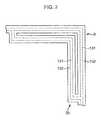
- FIG. 3is a sectional view showing a section taken along the I-I line in FIG. 1;
- FIG. 4is a layout showing the structure of a resistance value measuring part of the first embodiment
- FIG. 5is a sectional view taken along the II-II line in FIG. 4;
- FIG. 6is a layout showing the structure of wall parts of a semiconductor device according to a second embodiment of the present invention.
- FIG. 7is a layout showing the structure of wall parts of a semiconductor device according to a third embodiment of the present invention.
- FIG. 8is a layout showing the structure of wall parts of a semiconductor device according to a fourth embodiment of the present invention.
- FIG. 9is a layout showing the structure of wall parts of a semiconductor device according to a fifth embodiment of the present invention.
- FIG. 10is a layout showing the structure of wall parts of a semiconductor device according to a sixth embodiment of the present invention.
- FIG. 11is a layout showing the structure of wall parts of a semiconductor device according to a seventh embodiment of the present invention.
- FIG. 12is a layout showing the structure of wall parts of a semiconductor device according to an eighth embodiment of the present invention.
- FIG. 13is a layout showing the structure of wall parts of a semiconductor device according to a ninth embodiment of the present invention.
- FIG. 14is a layout showing the structure of wall parts of a semiconductor device according to a tenth embodiment of the present invention.
- FIG. 15is a layout showing the structure of wall parts of a semiconductor device according to an eleventh embodiment of the present invention.
- FIG. 16is a layout showing the structure of wall parts of a semiconductor device according to a twelfth embodiment of the present invention.
- FIG. 17is a layout showing the structure of wall parts of a semiconductor device according to a thirteenth embodiment of the present invention.
- FIG. 18A to FIG. 18Mare schematic sectional views showing a method of manufacturing the semiconductor device according to the first embodiment of the present invention in process order;
- FIG. 19is a plane view showing a wafer after pads are formed
- FIG. 20is a layout showing a region shown by the broken line in FIG. 19 by enlarging the region
- FIG. 21is a sectional view showing one example of the structure of a main wall part 2 and a sub-wall part 3 ;
- FIG. 22is a layout showing the structure when replacement is applied to the twelfth embodiment shown in FIG. 16.
- FIG. 23A and FIG. 23Bare a plan view and a cross sectional view showing a phase shift mask according to a fourteenth embodiment of the present invention.
- FIG. 24A and FIG. 24Bare enlarged views showing the phase shift mask according to the fourteenth embodiment of the present invention.
- FIG. 25A to FIG. 25Care a plan view and cross sectional views showing a phase shift mask according to a fifteenth embodiment of the present invention.
- FIG. 26A and FIG. 26Bare enlarged views showing the phase shift mask according to the fifteenth embodiment of the present invention.
- FIG. 27A and FIG. 27Bare a plan view and a cross sectional view showing a phase shift mask according to a sixteenth embodiment of the present invention.
- FIG. 28A and FIG. 28Bare a plan view and a cross sectional view showing a phase shift mask according to a seventeenth embodiment of the present invention.
- FIG. 29A and FIG. 29Bare a plan view and a cross sectional view showing a phase shift mask according to an eighteenth embodiment of the present invention.
- FIG. 30A and FIG. 30Bare a plan view and a cross sectional view showing a phase shift mask
- FIG. 31is a view showing a side lobe (No. 1).
- FIG. 32is a view showing a side lobe (No. 2).
- FIG. 1is a layout showing the structure of a semiconductor device according to the first embodiment of the present invention.
- FIG. 2is a sectional view showing the structure of an integrated circuit part of the first embodiment, and
- FIG. 3is a sectional view showing a section taken along the I-I line in FIG. 1.
- FIG. 4is a layout showing the structure of a resistance value measuring part of the first embodiment, and
- FIG. 5is a sectional view taken along the II-II line in FIG. 4.
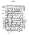
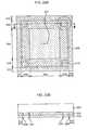
- a main wall part 2which is, for example, in a rectangular shape is provided so as to surround an integrated circuit part 1 in which a semiconductor integrated circuit is formed.
- the semiconductor device according to this embodimentis diced along the main wall part 2 outside the main wall part 2 , and is in a rectangular shape in plan view.
- a sub-wall part 3which is, for example, in an “L” shape is provided between each corner of the main wall part 2 and the integrated circuit part 1 . Portions of the sub-wall part 3 which are orthogonal to each other respectively extend in parallel to portions of the main wall part 2 which are orthogonal to each other, that is, the portions corresponding to its sides.
- a space between the main wall part 2 and the sub-wall part 3is, for example, about 1 ⁇ m. Further, a bend of the sub-wall part 3 is placed closest to a bend of the main wall part 2 , that is, a position corresponding to a vertex. Additionally, a resistance value measuring part (resistance value measuring means) 4 is provided between the sub-wall part 3 and the integrated circuit part 1 , for measuring a resistance value of the region.
- the sub-wall part 3is a first wall piece.
- a plurality of MOS transistors and the likeare formed as shown in FIG. 2.
- a semiconductor substrate 101such as a silicon substrate is demarcated into a plurality of element active regions by element isolation insulation films 102 .
- gate insulation films 103 and gate electrodes 104are formed on the semiconductor substrate 101 .
- sidewall insulation films 105are formed on the sides of the gate insulation films 103 and the gate electrodes 104 .
- source/drain diffusion layers 106are formed so as to sandwich the gate insulation films 103 and the gate electrodes 104 therebetween in plan view.
- a silicon nitride film 107 and a silicon oxide film 108are formed over the entire surface, and contact holes reaching the source/drain diffusion layers 106 are formed in the silicon nitride film 107 and the silicon oxide film 108 .
- the contact holeis, for example, about 0.10 to 0.20 ⁇ m in diameter.
- TiN films 109are formed as glue layers so as to cover the side surfaces and the bottom surfaces of the contact holes, in each of which a W film 110 is embedded.
- an organic insulation film 111 and a silicon oxide film 112are formed over the entire surface, and trenches 135 reaching the TiN films 109 and the W films 110 are formed in the organic insulation film 111 and the silicon oxide film 112 .
- Ta films 113are formed as barrier metal films so as to cover the side surfaces and the bottom surfaces of the trenches 135 , in each of which a wire 114 which is made of Cu or the like is embedded.
- a silicon nitride film 115 and a silicon oxide film 116are formed as interlayer insulation films over the entire surface, and contact holes 136 reaching the underlying wires, that is, the wires 114 , are formed in the silicon nitride film 115 and the silicon oxide film 116 .
- the contact holeis, for example, about 0.15 to 0.25 ⁇ m in diameter.
- an organic insulation film 117 and a silicon oxide film 118are formed over the entire surface, and trenches 137 which are connected to the contact holes 136 formed in the silicon nitride film 115 and the silicon oxide film 116 are formed in the organic insulation film 117 and the silicon oxide film 118 .
- Ta films 119are formed as barrier metal films so as to cover the side surfaces and the bottom surfaces of the contact holes 136 and the trenches 137 , in each of which a wire 120 which is made of Cu or the like is embedded.
- a plurality of basic structural bodies 121each of which is made of the silicon nitride film 115 , the silicon oxide film 116 , the organic insulation film 117 , the silicon oxide film 118 , the Ta films 119 and the wires 120 like the above, three of the basic structural bodies 121 in total in this embodiment, are provided.
- a silicon nitride film 122 and a silicon oxide film 123are formed on the uppermost basic structural body 121 , and contact holes 138 reaching the wires 120 , which constitute the uppermost basic structural body 121 , are formed in the silicon nitride film 122 and the silicon oxide film 123 .
- the contact holeis, for example, about 1.00 to 1.10 ⁇ m in diameter.
- barrier metal films 124are formed so as to cover the side surfaces and the bottom surfaces of the contact holes 138 and to cover a part of the surface of the silicon oxide film 123 , and Al or Al alloy films (hereinafter referred to as the Al film) 125 and barrier metal films 126 are formed on the barrier metal films 124 .
- a silicon oxide film 127is formed over the entire surface so as to cover the barrier metal films 124 , the Al films 125 and the barrier metal films 126 , and a silicon nitride film 128 , for example, is formed on the silicon oxide film 127 as a coating film.
- the two MOS transistors shown in FIG. 2constitute a CMOS transistor
- conduction types of the diffusion layers 106are different between the respective MOS transistors, and wells (not shown) are appropriately formed in the surface of the semiconductor substrate 101 .
- diffusion layers 106 aare formed in the surface of the semiconductor substrate 101 in the main wall part 2 and the sub-wall part 3 .
- Conduction types of the diffusion layers 106 aare not particularly limited.
- the silicon nitride film 107 and the silicon oxide film 108are formed over the entire surface, and trenches reaching the diffusion layers 106 a are formed in the silicon nitride film 107 and the silicon oxide film 108 .
- the trenchis, for example, about 0.15 to 0.30 ⁇ m in width.
- the TiN films 109are formed as the glue layers so as to cover the side surfaces and the bottom surfaces of the trenches, in each of which the W film 110 is embedded.
- the organic insulation film 111 and the silicon oxide film 112are formed over the entire surface, and trenches reaching the TiN films 109 and the W films 110 are formed in the organic insulation film 111 and the silicon oxide film 112 .
- the trenchis, for example, about 2 ⁇ m in width.
- Each of the trenchesis formed, for example, so that the TiN film 109 and the W film 110 are placed at its center.
- the Ta films 113are formed as the barrier metal films so as to cover the side surfaces and the bottom surfaces of the trenches, in each of which a metal film 114 a which is made of Cu or the like is embedded.
- the silicon nitride film 115 and the silicon oxide film 116are formed over the entire surface, and trenches reaching the underlying metal films, that is, the metal films 114 a , are formed in the silicon nitride film 115 and the silicon oxide film 116 .
- the trenchis, for example, about 0.20 to 0.35 ⁇ m in width.
- Each of the trenchesis formed to be placed at the center of the trench which is formed in the organic insulation film 111 and the silicon oxide film 112 , for example. Therefore, this trench is, for example, at the same position with the trench which is formed in the silicon nitride film 107 and the silicon oxide film 108 in plan view.
- the organic insulation film 117 and the silicon oxide film 118are formed over the entire surface, and trenches which are connected to the trenches formed in the silicon nitride film 115 and the silicon oxide film 116 are formed in the organic insulation film 117 and the silicon oxide film 118 .
- the trenchis, for example, about 2 ⁇ m in width. This trench is formed, for example, so that the trench formed in the silicon nitride film 115 and the silicon oxide film 116 is placed at its center. Therefore, this trench is, for example, at the same position with the trench which is formed in the organic insulation film 111 and the silicon oxide film 112 in plan view.
- the Ta films 119are formed as the barrier metal films so as to cover the side surfaces and the bottom surfaces of the trenches formed in the silicon nitride film 115 and the silicon oxide film 116 and the trenches formed in the organic insulation film 117 and the silicon oxide film 118 , in each of which a metal film 120 a which is made of a Cu film or the like is embedded.
- a plurality of basic structural bodies 121 aeach of which is made of the silicon nitride film 115 , the silicon oxide film 116 , the organic insulation film 117 , the silicon oxide film 118 , the Ta films 119 and the metal films 120 a like the above, three of the basic structural bodies 121 a in total in this embodiment, similarly to the integrated circuit part 1 , are provided.
- the silicon nitride film 122 and the silicon oxide film 123are formed on the uppermost basic structural body 121 a , and trenches reaching the metal films 120 a , which constitute the uppermost basic structural body 121 a , are formed in the silicon nitride film 122 and the silicon oxide film 123 .
- the trenchis, for example, about 1.15 to 1.25 ⁇ m in width.
- the barrier metal films 124are formed so as to cover the side surfaces and the bottom surfaces of the trenches and to cover a part of the surface of the silicon oxide film 123 , and the Al films 125 and the barrier metal films 126 are formed on the barrier metal films 124 .
- the silicon oxide film 127is formed over the entire surface so as to cover the barrier metal films 124 , the Al films 125 and the barrier metal films 126 , and the silicon nitride film 128 , for example, is formed on the silicon oxide film 127 as the coating film.
- the trench formed in the silicon nitride film 115 and the silicon oxide film 116 and a narrow trench 131 formed in the silicon nitride film 122 and the silicon oxide film 123are shorter than the trench formed in the organic insulation film 111 and the silicon oxide film 112 and a wide trench 132 formed in the organic insulation film 117 and the silicon oxide film 118 and, as shown in FIG. 1, both end parts of the narrow trench 131 are placed inside both end parts of the wide trench 132 .
- two comb-like electrodes 5 a and 5 bare provided in the resistance value measuring part 4 . Teeth of the comb-like electrodes 5 a and 5 b are arranged in an alternating manner. Each of monitor pads for checking to secure moisture resistance 6 a and 6 b is connected to one end of each comb-like electrode 5 a and 5 b . Further, in the region between the integrated circuit part 1 and the main wall part 2 where the sub-wall part 3 and the resistance value measuring part 4 are not formed, a plurality of evaluation pads 7 for inputting signals from the outside in evaluating the integrated circuit formed in the integrated circuit part 1 are provided at appropriate intervals.
- the sectional structure of the comb-like electrodes 5 a and 5 bis the same as that of the main wall part 2 and the sub-wall part 3 , except that the metal films are not connected to the substrate. However, the widths of the trenches are different.
- the trench formed in the silicon nitride film 115 and the silicon oxide film 116 and the narrow trench 133 formed in the silicon nitride film 122 and the silicon oxide film 123are, for example, about 0.20 to 0.35 ⁇ m in width
- the trench formed in the organic insulation film 111 and the silicon oxide film 112 and the wide trench 134 formed in the organic insulation film 117 and the silicon oxide film 118are, for example, about 0.6 ⁇ m in width.
- spaces between the teeth of the comb-like electrodes 5 a and 5 bare, for example, about 0.2 ⁇ m.
- a part of the Al films 125is exposed from the silicon nitride film 128 and the silicon oxide film 127 to make the pads 6 a and 6 b.
- the sub-wall part 3 in the “L” shapeis selectively provided inside the main wall part 2 in the rectangular shape in plan view, and at each of the four corners of the main wall part 2 , at which stress is most concentrated, and a plurality of the metal films constituting the main wall part 2 and the sub-wall part 3 are connected to the semiconductor substrate 101 , and hence, the stress is easily dispersed at the corners. Therefore, even if the stress is concentrated due to heat treatment or the like, peeling between layers and a crack are unlikely to occur, as compared with the conventional art.
- the position where the sub-wall part 3 is formedis the region where the pads and the like are not formed and the element particularly affecting the function of the semiconductor device does not exist in the conventional art, a chip area hardly increases even when the sub-wall part 3 is provided at this position.
- the main wall part 2 and the sub-wall part 3can be formed by changing mask shapes in forming the silicon nitride film, the silicon oxide film, the organic insulation film, the wire and the like which constitute the integrated circuit part 1 , and therefore, it is also possible to avoid the increase in the number of manufacturing processes.
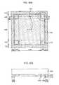
- FIG. 6is a layout showing the structure of wall parts of a semiconductor device according to the second embodiment of the present invention.
- the structure of a sub-wall partis different from that of the first embodiment.
- the length of a narrow trench 131 and the length of a wide trench 132 in a sub-wall part 3 aare the same with reference to a bending point, and, respective end parts are at the same positions in plan view.
- the structure of a section of each position of the sub-wall part 3 a which crosses perpendicularly to a direction toward which the trenches extendis the same as that of the sub-wall part 3 in the first embodiment, except for the lengths of the trenches as described above.
- the sub-wall part 3 ais a first wall piece.
- FIG. 7is a layout showing the structure of wall parts of a semiconductor device according to the third embodiment of the present invention.
- a sub-wall part 3 bhas a plan shape in which both end parts of the sub-wall part 3 of the first embodiment are bent perpendicularly toward the main wall part 2 side and are connected to the main wall part 2 .
- a narrow trench 131 in the sub-wall part 3 bis connected to a narrow trench 131 in the main wall part 2
- a wide trench 132 in the sub-wall part 3 bis connected to a wide trench 132 in the main wall part 2 .
- the structure of a section of each position of the sub-wall part 3 b which crosses perpendicularly to a direction toward which the trenches extendis the same as that of the sub-wall part 3 in the first embodiment, except for the plan shape as described above.
- the sub-wall part 3 bis a first wall piece.
- FIG. 8is a layout showing the structure of wall parts of a semiconductor device according to the fourth embodiment of the present invention.
- a plan shape of a sub-wall part 3 cis a rectangular shape.
- the structure of a section of each position of the sub-wall part 3 c which crosses perpendicularly to a direction toward which the trenches extendis the same as that of the sub-wall part 3 in the first embodiment, except for the plan shape as described above.
- comb-like electrodes 5 a and 5 b(not shown in FIG. 8) which constitute a resistance value measuring part 4 are arranged, for example, so as to sandwich the sub-wall part 3 c between the main wall part 2 and themselves.
- the comb-like electrodes 5 a and 5 bare arranged, for example, along two sides which are alienated from a vertex of the main wall part 2 , out of four sides constituting the sub-wall part 3 c in the rectangular shape in plan view.
- the sub-wall part 3 cis a fourth wall piece.
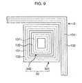
- FIG. 9is a layout showing the structure of wall parts of a semiconductor device according to the fifth embodiment of the present invention.
- the structure of a sub-wall partis different from that of the first embodiment.
- a plurality of wall pieces, two rectangular wall pieces 3 d 1 and 3 d 2 in this embodimentare provided as a sub-wall part 3 d .
- the wall piece 3 d 2is a fourth wall piece
- the wall piece 3 d 1is a fifth wall piece.
- the structure of a section of each position of the wall pieces 3 d 1 and 3 d 2 constituting the sub-wall part 3 d which crosses perpendicularly to a direction toward which the trenches of extendis the same as that of the sub-wall part 3 in the first embodiment, except for the plan shape as described above.
- the sub-wall part 3 dmay be structured by three or more of the wall pieces.
- FIG. 10is a layout showing the structure of wall parts of a semiconductor device according to the sixth embodiment of the present invention.
- the structure of a sub-wall partis different from that of the first embodiment.
- a plurality of, for example, three wall pieces 3 e 1 to 3 e 3are arranged at, for example, regular intervals from a corner of the main wall part 2 toward an integrated circuit part 1 side, to constitute a sub-wall part 3 e .
- Each of the wall pieces 3 e 1 to 3 e 3has the same structure as that of the sub-wall part 3 of the first embodiment.
- the wall pieces 3 e 1 to 3 e 3are first wall pieces.
- the sub-wall part 3 emay be structured by two or four or more wall pieces each of which has the same structure as that of the sub-wall part 3 .
- FIG. 11is a layout showing the structure of wall parts of a semiconductor device according to the seventh embodiment of the present invention.
- the structure of a sub-wall partis different from that of the first embodiment.
- a wall piece 3 f 1which is shorter than a wall piece 3 f 2 is arranged on an integrated circuit part 1 side from the wall piece 3 f 2 which has the same structure as that of the sub-wall part 3 of the first embodiment, to constitute a sub-wall part 3 f .
- the structure of a section of each position of the wall piece 3 f 1 which crosses perpendicularly to a direction toward which the trenches extendis the same as that of the sub-wall part 3 in the first embodiment.
- the wall piece 3 f 2is a first wall piece
- the wall piece 3 f 1is a second wall piece.
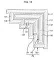
- FIG. 12is a layout showing the structure of wall parts of a semiconductor device according to the eighth embodiment of the present invention.
- the structure of a sub-wall partis different from that of the first embodiment.
- a wall piece 3 g 1which surrounds the wall pieces 3 f 1 and 3 f 2 of the seventh embodiment with the main wall part 2 is arranged to constitute a sub-wall part 3 g .
- the structure of a section of each position of the wall piece 3 g 1 which crosses perpendicularly to a direction toward which the trenches extendis the same as that of the sub-wall part 3 in the first embodiment.
- the wall piece 3 g 1is a third wall piece.
- FIG. 13is a layout showing the structure of wall parts of a semiconductor device according to the ninth embodiment of the present invention.
- the structure of a sub-wall partis different from that of the first embodiment.
- wide trenches 132 awhich are the same as the trenches 132 of the wall pieces 3 f 1 and 3 f 2 of the seventh embodiment are formed in the organic insulation film 117 and the silicon oxide film 118 which exist between the wall pieces 3 f 1 and 3 f 2 , and the Ta films 119 and the metal films 120 a are embedded in the trenches 132 a , to constitute a sub-wall part 3 h.
- FIG. 14is a layout showing the structure of wall parts of a semiconductor device according to the tenth embodiment of the present invention.
- the structure of a sub-wall partis different from that of the first embodiment.
- the wide trenches 132 awhich are the same as the trenches 132 of the wall pieces 3 f 1 and 3 f 2 of the seventh embodiment are formed in the organic insulation film 117 and the silicon oxide film 118 which exist between the wall pieces 3 f 1 and 3 f 2 .
- narrow trenches 131 awhich are the same as the trenches 131 of the wall pieces 3 f 1 and 3 f 2 are formed in the silicon nitride film 115 and the silicon oxide film 116 which exist between the wall pieces 3 f 1 and 3 f 2 .
- the Ta films 119 and the metal films 120 aare embedded in the trenches 131 a and 132 a , to constitute a sub-wall part 3 i.
- FIG. 15is a layout showing the structure of wall parts of a semiconductor device according to the eleventh embodiment of the present invention.
- the structure of a sub-wall partis different from that of the first embodiment.
- a sub-wall part 3 jwhich is in an “L” shape and both of whose ends are connected to the main wall part 2 is provided.
- the structure of a section of each position of the sub-wall part 3 j which crosses perpendicularly to a direction toward which the trenches extendis the same as that of the sub-wall part 3 in the first embodiment.
- the sub-wall part 3 jis a sixth wall piece.
- FIG. 16is a layout showing the structure of wall parts of a semiconductor device according to the twelfth embodiment of the present invention.
- a sub-wall parthas the structure in which the sub-wall part 3 d of the fifth embodiment and the sub-wall part 3 j of the eleventh embodiment are combined.
- the wall pieces 3 d 1 and 3 d 2 of the fifth embodimentare disposed in a square-shaped region existing between a wall piece 3 k 1 which has the same structure as that of the sub-wall part 3 j of the eleventh embodiment and the main wall part 2 , to constitute a sub-wall part 3 k .
- the wall piece 3 k 1is a sixth wall piece.
- FIG. 17is a layout showing the structure of wall parts of a semiconductor device according to the thirteenth embodiment of the present invention.
- the structure of a sub-wall partis different from that of the twelfth embodiment.
- the wide trench 132extends to the organic insulation film 117 and the silicon oxide film 118 which exist between the wall pieces 3 d 1 and 3 d 2 constituting the sub-wall part 3 k of the twelfth embodiment, and further to the inside of the square-shaped region in the wall piece 3 d 2 .
- the Ta film 119 and the metal film 120 aare embedded in the trench 132 , to constitute a sub-wall part 3 m.
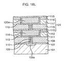
- FIG. 18A to FIG. 18Mare schematic sectional views showing the method of manufacturing the semiconductor device according to the first embodiment of the present invention in process order. Incidentally, only the region corresponding to the main wall part 2 will be illustrated in FIG. 18A to FIG. 18M.
- the element isolation insulation film 102is formed on the surface of the semiconductor substrate 101 in a state of a wafer by, for example, the LOCOS method, the STI method or the like. Thereafter, the gate insulation film 103 , the gate electrode 104 , the sidewall insulation film 105 and the source/drain diffusion layer 106 are formed in the integrated circuit part 1 . Further, in the main wall part 2 and the sub-wall part 3 , the diffusion layers 106 a and 106 b are selectively formed simultaneously with the formation of the source/drain diffusion layer 106 . Next, the silicon nitride film 107 and the silicon oxide film 108 are formed over the entire surface by, for example, the plasma CVD method.
- the silicon nitride film 107 and the silicon oxide film 108are, for example, 70 nm and 1000 nm in thickness, respectively.
- the silicon oxide film 108is flattened by, for example, the chemical mechanical polishing (CMP), thereby eliminating the difference in levels.
- CMPchemical mechanical polishing
- the silicon oxide film 108is, for example, 700 nm in thickness.
- a photoresist 201is applied onto the silicon oxide film 108 , and the photoresist 201 is exposed and developed. Thereby, a pattern 201 a for forming the contact hole in the integrated circuit part 1 and the narrow trenches 131 and 133 in the main wall part 2 and the sub-wall part 3 is formed in the photoresist 201 .
- the element isolation insulation filmmay be formed on the surface of the semiconductor substrate 101 over the entire region of the resistance value measuring part 4 , simultaneously with the formation of the element isolation insulation film 102 , for example.
- the element isolation insulation filmmay be formed on the surface of the semiconductor substrate 101 only in the region where the electrodes 5 a and 5 b are to be formed.
- the photoresist 201as a mask, the silicon oxide film 108 and the silicon nitride film 107 are subjected to anisotropic etching using a CF group gas. Thereby, the contact hole is formed in the integrated circuit part 1 , and the narrow trenches 131 and 133 are formed in the main wall part 2 , the sub-wall part 3 and the resistance value measuring part 4 . Thereafter, the photoresist 201 is removed, and the TiN film 109 is formed as the glue layer in the contact hole, the narrow trenches 131 and 133 and on the silicon oxide film 108 by, for example, the sputtering, the CVD method or the like.
- the W film 110is formed on the TiN film 109 by, for example, the CVD method or the like.
- the TiN film 109is, for example, 50 nm in thickness
- the W film 110is, for example, 400 nm in thickness.
- the TiN film 109 and the W film 110 on the silicon oxide film 108are removed by the CMP method or the like, so that the TiN film 109 and the W film 110 remain only in the contact hole and the narrow trenches 131 and 133 .
- an organic insulation film materialis applied by, for example, the spin coating over the entire surface. Then, the organic insulation film material undergoes heat treatment which is suitable for this material, for example, the heat treatment at 400° C. for 60 minutes. Thereby, the organic insulation film material is hardened and the organic insulation film 111 is formed. Further, the silicon oxide film 112 is formed on the organic insulation film 111 . Both of the organic insulation film 111 and the silicon oxide film 112 are, for example, 250 nm in thickness. Thereafter, a photoresist 202 is applied onto the silicon oxide film 112 , and the photoresist 202 is exposed and developed.
- a pattern 202 a for forming the trench 135 for the wire in the integrated circuit part 1 and the wide trenches 132 and 134 in the main wall part 2 , the sub-wall part 3 and the resistance value measuring part 4is formed in the photoresist 202 .
- the silicon oxide film 112is subjected to the anisotropic etching by using the photoresist 202 as a mask, and thereafter, the organic insulation film 111 is subjected to the etching using a mixed gas of H 2 and N 2 .
- the trench 135is formed in the integrated circuit part 1
- the wide trenches 132 and 134are formed in the main wall part 2 , the sub-wall part 3 and the resistance value measuring part 4 .
- the photoresist 202is removed together with the organic insulation film 111 , but the silicon oxide film 112 which exists underneath thereof is not subjected to the etching.
- the Ta film 113is formed as the barrier metal film in the trenches 135 , 132 and 134 and on the silicon oxide film 112 by, for example, the sputtering or the like. Further, a film for wire material to become the wire 114 and the metal film 114 a , for example, the Cu film, is formed on the Ta film 113 by, for example, the plating method or the like. It should be noted that, when the film for wire material is formed by the plating method, it is preferable to form a seed layer after forming the Ta film 113 by the sputtering, and thereafter, to form the film for wire material.
- the Ta film 113is, for example, 30 nm in thickness and the film for wire material is, for example, 1800 nm in thickness.
- the Ta film 113 and the film for wire material on the silicon oxide film 112are removed by the CMP method or the like, so that the Ta film 113 and the film for wire material remain only in the trenches 135 , 132 and 134 .
- the wire 114 and the metal film 114 aare formed.
- the silicon nitride film 115 and the silicon oxide film 116are formed over the entire surface in sequence.
- the silicon nitride film 115is, for example, 50 nm in thickness
- the silicon oxide film 116is, for example, 800 nm in thickness.
- the silicon nitride film 115functions as an etching stopper film and a diffusion preventing film.
- the silicon oxide film 116is flattened by, for example, the CMP, thereby eliminating the difference in levels.
- the silicon oxide film 116is, for example, 400 nm in thickness.
- the silicon oxide film 116 having the thickness of, for example, about 400 nmmay be formed on the silicon nitride film 115 in order to omit the process of the CMP.
- the organic insulation film 117 and the silicon oxide film 118are formed on the silicon oxide film 116 in sequence.
- the organic insulation film 117can be formed by applying, for example, the organic insulation film material by the spin coating, allowing the organic insulation film material to undergo the appropriate heat treatment and hardening the organic insulation film material.
- the organic insulation film 117 and the silicon oxide film 118are, for example, 250 nm in thickness.
- a metal film 203 which is used as a hard mask in forming the trenchis formed on the silicon oxide film 118 .
- the metal film 203is, for example, the TiN film, and its thickness is, for example, 100 nm.
- a photoresist 204is applied on the metal film 203 , and the photoresist 204 is exposed and developed. Thereby, a pattern 204 a for forming the trench 137 in the integrated circuit part 1 and the wide trenches 132 and 134 in the main wall part 2 , the sub-wall part 3 and the resistance value measuring part 4 is formed in the photoresist 204 .
- the metal film 203is subjected to the etching using a Cl type gas. Thereby, the pattern 204 a is transferred to the metal film 203 to form a pattern 203 a . Then, the photoresist 204 is removed by the ashing. Next, a photoresist 205 is applied over the entire surface, and the photoresist 205 is exposed and developed.
- a pattern 205 a for forming the contact hole 136 in the integrated circuit part 1 and the narrow trenches 131 and 133 in the main wall part 2 , the sub-wall part 3 and the resistance value measuring part 4is formed in the photoresist 205 .
- the silicon oxide film 118is subjected to the etching by using the photoresist 205 as a mask. Further, by using the silicon oxide film 118 as a mask, the organic insulation film 117 is subjected to the etching using a mixed gas of H 2 and N 2 , thereby forming the contact hole 136 in the integrated circuit part 1 and the narrow trenches 131 and 133 in the main wall part 2 , the sub-wall part 3 and the resistance value measuring part 4 . At this time, the photoresist 205 is removed together with the organic insulation film 117 , but the metal film 203 and the silicon oxide film 118 which exist underneath thereof are not subjected to the etching.
- the silicon oxide films 118 and 116are subjected to the etching by using the metal film 203 and the organic insulation film 117 as masks.
- the pattern 203 ais transferred to the silicon oxide film 118
- the patterns formed in the silicon oxide film 118 and the organic insulation film 117are transferred to the silicon oxide film 116 .
- the etching of the silicon oxide film 118stops on the organic insulation film 117
- the etching of the silicon oxide film 116stops on the silicon nitride film 115 , which functions as the etching stopper film.
- the organic insulation film 117is subjected to the anisotropic etching using the metal film 203 and the silicon oxide film 118 as masks. Thereafter, the silicon nitride film 115 is subjected to the anisotropic etching using the silicon oxide film 116 as a mask. Consequently, the contact hole 136 and the trench 137 are formed in the integrated circuit part 1 , the trenches 131 and 133 are formed in the main wall part 2 and the sub-wall part 3 , and the trenches 132 and 134 are formed in the resistance value measuring part 4 .
- the anisotropic etching of the organic insulation film 117may be carried out after the anisotropic etching of the silicon nitride film 115 .
- the Ta film 119is formed as the barrier metal film in the trenches 131 to 135 , the contact hole 136 and on the metal film 203 which come to the surface by, for example, the sputtering or the like.
- a film for wire material to become the wire 120 and the metal film 120 ais formed on the Ta film 119 by, for example, the plating method or the like. It should be noted that, when the film for wire material is formed by the plating method, it is preferable to form a seed layer after forming the Ta film 119 by the sputtering, and thereafter, to form the film for wire material.
- the Ta film 119is, for example, 30 nm in thickness and the film for wire material is, for example, 1800 nm in thickness.
- the metal film 203 , the Ta film 119 and the film for wire material on the silicon oxide film 118are removed by the CMP method or the like, so that the Ta film 119 and the film for wire material remain only in the trenches 131 to 135 and in the contact hole 136 which came to the surface.
- the metal film 120 ais formed in the main wall part 2 , the sub-wall part 3 , and the resistance value measuring part 4 , and the wire 120 (not shown in FIG. 18L) is formed in the integrated circuit part 1 .
- the silicon nitride film 115is formed again over the entire surface, and the process shown in FIG. 18F to the process shown in FIG. 18L are repeated for a predetermined number of times.
- the silicon nitride film 122 and the silicon oxide film 123are formed over the entire surface.
- the trenches 131 and 133 and the contact hole 138are formed in the silicon oxide film 123 and the silicon nitride film 122 using a photoresist (not shown) in which a predetermined pattern is formed.
- the barrier metal film 124 and the Al film 125are formed in the trenches 131 and 133 , the contact hole 138 and on the silicon oxide film 123 , and further, the barrier metal film 126 is formed on the Al film 125 .
- the barrier metal film 126 , the Al film 125 and the barrier metal film 124are patterned into predetermined shapes, on which the silicon oxide film 127 is formed over the entire surface. Then, the silicon nitride film 128 is formed on the silicon oxide film 127 as the coating film.
- FIG. 19is a plane view showing the wafer after the pads are formed
- FIG. 20is a layout showing a region shown by the broken line in FIG. 19 by enlarging the region.
- phase shift maskof, for example, a halftone type is used in patterning a photoresist.
- FIG. 30A and FIG. 30Bare a plan view and a cross sectional view showing a phase shift mask.
- FIG. 30Ais a plan view and FIG. 30B is a cross sectional view taken along the III-III line in FIG. 30A.
- a translucent phase shifter film 402is formed on a transparent substrate 400 .
- the phase shifter film 402for example, one which shifts the phase of lights transmitting therethrough by 180 degrees is used.
- the phase shifter film 402has contact hole patterns 407 formed therein.
- the contact hole patterns 407are intended for forming contact holes.
- the phase shifter film 402has a main wall part pattern 408 and a sub-wall part pattern 410 formed therein.
- the main wall part pattern 408is a pattern for forming the main wall part 2 (refer to FIG. 1).
- the sub-wall part pattern 410is a pattern for forming the sub-wall part 3 (refer to FIG. 1).
- a light shield film 414is formed on the phase shifter film 402 .
- the scribe line region 412is a region where adjacent shots overlap each other on a wafer when transfer and exposure are subsequently conducted using a stepper (multiple exposure region).
- the use of the halftone phase shift maskcauses a phase difference of 180 degrees between a light passing through the phase shifter film 402 and a light passing through a transmitting region so that the contrast in the vicinity of a pattern edge can be enhanced due to interference of light. This enables microscopic formation of the integrated circuit part.
- a side lobeis sometimes generated in the vicinity of these patterns.
- the side lobeis generated by mutual interference of lights passing through a pattern constituted of the translucent phase shifter film. Since the main wall part pattern 408 and the sub-wall part pattern 410 are formed to be linear, the exposure amount therein is larger compared with that in the contact hole patterns 407 . Accordingly, the side lobe is liable to occur in the vicinity of the main wall part and the sub-wall part.
- FIG. 31is a view showing a side lobe (No. 1).
- FIG. 32is a view showing a side lobe (No. 2) As shown by the arrows in FIG. 31 and FIG. 32, side lobes are generated in the vicinity of a part having an L-shaped pattern and a part having a T-shaped pattern. Further, a side lobe is sometimes generated also in a part having a linear shaped pattern, though not shown.
- Japanese Patent Laid-open No. 8-279452discloses a technique for preventing the generation of the side lobe by forming a dummy opening region.
- optimizationis necessary every time lighting conditions and so on of photolithography are varied, which requires an enormous amount of work.
- itis extremely difficult to prevent a side lobe generated in a part having a linear pattern.
- phase shift maskas structured below makes it possible to manufacture the aforesaid semiconductor device while preventing the occurrence of the side lobe.
- a phase shift mask according to a fourteenth embodiment of the present inventionwill be explained using FIG. 23A, FIG. 23B, FIG. 24A, and FIG. 24B.
- FIG. 23A and FIG. 23Bare a plan view and a cross sectional view showing the phase shift mask according to this embodiment.
- FIG. 23Ais a plan view and FIG. 23B is a cross sectional view taken along the III-III line in FIG. 23A.
- FIG. 24A and FIG. 24Bare enlarged views showing the phase shift mask according to this embodiment.
- FIG. 24A and FIG. 24Bshow enlarged views of a circled region in FIG. 23A.
- FIG. 24Ais a plan view and FIG. 24B is a cross sectional view taken along the III-III line in FIG. 24A.
- a part of wall part piece patterns 309 b(refer to FIG. 24A and FIG.
- FIG. 24Bthe wall part piece patterns 309 b omitted in FIG. 23A and FIG. 23B are also shown in FIG. 24A and FIG. 24B.
- the same reference numerals and symbolsare used to designate the same constituent elements as those of the semiconductor devices and the method of manufacturing the same according to the first to thirteenth embodiments shown in FIG. 1 to FIG. 22, and the explanation thereof will be omitted or simplified.
- a phase shift mask used in patterning the photoresist 201 shown in FIG. 18Awill be taken for example to explain this embodiment.
- a phase shift mask used in forming, in the photoresist 201 , the pattern 201 a and so on for forming the contact holes reaching the source/drain diffusion layer 106 (refer to FIG. 2) and the trenches 131 (refer to FIG. 1) reaching the diffusion layer 106 a (refer to FIG. 3)will be taken for example to explain this embodiment.
- phase shift mask for patterning the photoresist 201 shown in FIG. 18Awill be taken for example for explanation, but the principle of the present invention is applicable to a phase shift mask for patterning all the other photoresists such as the photoresist 202 (refer to FIG. 18C), the photoresist 204 (refer to FIG. 18F), the photoresist 205 (refer to FIG. 18G), and the like.
- a phase shifter film 302is formed on a transparent substrate 300 .
- a material of the phase shifter film 302for example, a material whose light transmittance is about 4% to about 30% and which shifts the phase of a light by 180 degrees is usable. More specifically, as the material of the phase shifter film 302 , for example, MoSi (molybdenum silicide) or the like is usable.
- the phase shifter film 302has contact hole patterns 307 formed therein.
- the contact hole patterns 307are patterns for forming contact holes as described above.
- the phase shifter film 302has a main wall part pattern 308 and a sub-wall part pattern 310 formed therein.
- the main wall part pattern 308is a pattern for forming the main wall part 2 (refer to FIG. 1) as described above.
- the sub-wall part pattern 310is a pattern for forming the sub-wall part 3 (refer to FIG. 1) as described above.
- the sub-wall part pattern 310is constituted of a wall part piece pattern 309 a and wall part piece patterns 309 b .
- the wall part piece pattern 309 a on the outer sideis formed in an L shape as a whole.
- the plurality of wall part piece patterns 309 b on the inner sideare formed.
- the shape of each of the wall part piece patterns 309 b on the inner sideapproximates that of the contact hole pattern 307 .
- the plural wall part piece patterns 309 bare arranged in a “square” shape as a whole.
- the plural wall part piece patterns 309 b arranged in the “square” shape as a wholeare arranged in a single square here, but the arrangement of the plural wall part piece patterns 309 b arranged in the “square” shape as a whole is not limited to a single square and may be arranged in a two squares or more.
- the wall part piece pattern 309 a on the outer sideis connected to the main wall part pattern 308 . Portions where the main wall part pattern 308 and the wall part piece pattern 309 a of the sub-wall part pattern 310 are connected to each other are formed in a T-shaped pattern.
- a light shield film 314consisting of, for example, Cr is formed.
- the light shield film 314is formed also in the peripheral edge region 306 .
- the reason for forming the light shield film 314 also in the peripheral edge region 306 in this embodimentis explained as follows.
- the light shield film 314prevents lights from passing through the phase shifter film 302 so that the occurrence of the interference of the lights in the peripheral edge region 306 can be reduced. This enables the prevention of the occurrence of the side lobe in the peripheral edge region 306 .
- the light shield film 314is formed so as to cover a range extending to, for example, about 1 ⁇ m to about 5 ⁇ m inward from corners of the sub-wall part pattern 310 .
- the size of patterns formed in the peripheral edge region 306is relatively larger than the size of patterns formed in the integrated circuit region 304 .
- the patterns formed in the peripheral edge region 306include, besides the main wall part pattern 308 and the sub-wall part pattern 310 , contact hole patterns (not shown) and so on. The reason for making the size of the patterns in the peripheral edge region larger than the size of the patterns in the integrated circuit region is explained as follows.
- the width of the main wall part 2 (refer to FIG. 1) and the sub-wall part 3 (refer to FIG. 1)is, for example, about 0.2 ⁇ m to about 10 ⁇ m on a wafer which is an image plane, and the diameter of a contact hole (not shown) of the integrated circuit part 1 (refer to FIG.
- the halftone phase shift mask according to this embodimentis structured.
- the main characteristic of the phase shift mask according to this embodimentlies in that the light shield film 314 is formed also in the peripheral edge region 306 as described above.
- phase shift mask shown in FIG. 30A and FIG. 30BWhen the phase shift mask shown in FIG. 30A and FIG. 30B is used, lights passing through the phase shifter film 302 interfere with each other in the vicinity of the main wall part and the sub-wall part to generate the side lobe in the vicinity of the main wall part and the sub-wall part.
- the light shield film 314is formed also in the peripheral edge region 306 so that the light shield film 314 can prevent lights from passing through the phase shifter film 302 in the peripheral edge region 306 . Therefore, according to this embodiment, the mutual interference of the lights in the vicinity of the main wall part 2 and the sub-wall part 3 can be reduced to enable the prevention of the side lobe generation.
- the phase shift maskcan be manufactured without increasing the number of manufacturing processes.
- FIG. 25A to FIG. 25Care a plan view and cross sectional views showing the phase shift mask according to this embodiment.
- FIG. 25Ais a plan view
- FIG. 25Bis a cross sectional view taken along the III-III line in FIG. 25A
- FIG. 25Cis a cross sectional view taken along the IV-IV line in FIG. 25A.
- FIG. 26A and FIG. 26Bare enlarged views showing the phase shift mask according to this embodiment.
- FIG. 26A and FIG. 26Bshow enlarged views of a circled part in FIG. 25A.
- FIG. 26Ais a plan view and FIG.
- 26Bis a cross sectional view taken along the III-III line in FIG. 26A. Though a part of the wall part piece patterns 309 b (refer to FIG. 26A and FIG. 26B) is omitted in FIG. 25A to FIG. 25C, the wall part piece patterns 309 b omitted in FIG. 25A to FIG. 25C are also shown in FIG. 26A and FIG. 26B. Further, though a part of contact hole patterns 316 (refer to FIG. 26A and FIG. 26B) is omitted in FIG. 25A to FIG. 25C, the contact hole patterns 316 omitted in FIG. 25A to FIG. 25C are also shown in FIG. 26A and FIG. 26B.
- the main characteristic of the phase shift mask according to this embodimentlies in that the light shield film 314 is selectively formed only in the vicinity of the main wall part pattern 308 and the sub-wall part pattern 310 .
- the light shield film 314is selectively formed only in the vicinity of the main wall part pattern 308 and the sub-wall part pattern 310 in the peripheral edge region 306 .
- the light shield film 314is formed so as to cover a range extending to, for example, about 1 ⁇ m to about 5 ⁇ m inward from the edges of the main wall part pattern 308 and the sub-wall part pattern 310 .
- the range in which the light shield film 314 is formedis not limited to the range of 1 ⁇ m to 5 ⁇ m inward from the edges of the main wall part pattern 308 and the sub-wall part pattern 310 .
- the range in which the light shield film 314 is formedmay be appropriately set to such an extent that the side lobe generation can be prevented.
- the light shield film 314is not formed in regions of the peripheral edge region 306 except the vicinity of the main wall part pattern 308 and the sub-wall part pattern 310 .
- the contact hole patterns 316are formed in the region of the peripheral edge region 306 where the light shield film 314 is not formed.
- the contact hole patterns 316are patterns for forming contact holes (not shown) reaching a source/drain diffusion layer of MOS transistors, for example.
- the light shield film 314is formed in the scribe line region 312 similarly to the above description.
- the main characteristic of the phase shift mask according to this embodimentlies in that the light shield film 314 is formed on the phase shifter film 302 only in the vicinity of the main wall part pattern 308 and the sub-wall part pattern 310 as described above.
- the light shield film 314is formed all over the peripheral edge region 306 . Since the resolution tends to be low in a region where the light shield film 314 is formed, microscopic contact holes cannot be formed inside the peripheral edge part when the phase shift mask according to the fourteenth embodiment is used. Accordingly, microscopic MOS transistors cannot be formed in the peripheral edge part when the phase shift mask according to the fourteenth embodiment is used.
- the light shield film 314is selectively formed only in the vicinity of the main wall part pattern 308 and the sub-wall part pattern 310 in the peripheral edge region 306 . Therefore, according to this embodiment, a high resolution is obtainable in the region of the peripheral edge region 306 where the light shield film 314 is not formed. Consequently, according to this embodiment, microscopic contact holes can be formed also in the peripheral edge part. Therefore, according to this embodiment, microscopic elements such as MOS transistors can be formed also in the peripheral edge part. According to this embodiment, it is possible to secure a wide space for a region in which microscopic elements such as MOS transistors can be formed, which can contribute to the reduction in chip size.
- FIG. 27A and FIG. 27Bare a plan view and a cross sectional view showing the phase shift mask according to this embodiment.
- the same reference numerals and symbolsare used to designate the same constituent elements as those of the semiconductor devices, the method of manufacturing the same, and the phase shift masks according to the first to fifteenth embodiments shown in FIG. 1 to FIG. 26B, and the explanation thereof will be omitted or simplified.
- the main characteristics of the phase shift mask according to this embodimentlie in that the light shield film 314 is not formed in the peripheral edge region 306 , that corner portions of the main wall part pattern 308 a and a sub-wall part pattern 310 a do not have a right angle but they have an obtuse angle, and that the main wall part pattern 308 a and the sub-wall part pattern 310 a are formed so as to be insolated from each other.
- the light shield film 314is not formed in the peripheral edge region 306 in this embodiment.
- the corner portion of the main wall part pattern 308 adoes not have a right angle but has an obtuse angle. Concretely, the angle of the corner portion of the main wall part pattern 308 a is 135 degrees.
- the sub-wall part pattern 310 ais constituted of a wall part piece pattern 309 c and the wall part piece patterns 309 b .
- the corner portion of the wall part piece pattern 309 cdoes not have a right angle but has an obtuse angle. Concretely, the angle of the corner portion of the wall part piece pattern 309 c is 135 degrees.
- the reason why the corner portions of the main wall part pattern 308 a and the sub-wall part pattern 310 a do not have a right angle but has an obtuse angle in this embodimentis to eliminate portions having an L-shaped pattern to prevent the generation of the side lobe.
- the angle of the corner portions of the main wall part pattern 308 a and the sub-wall part pattern 310 ais not limited to 135 degrees.
- the generation of the side lobecan be reduced to some extent. Specifically, when the angle of the corner portions is 100 degrees or larger, the generation of the side lobe can be effectively reduced. When the angle of the corner portions is 110 degrees or larger, the generation of the side lobe can be more effectively reduced. Further, when the angle of the corner portions is 120 degrees or larger, the generation of the side lobe can be still more effectively reduced.
- the main wall part pattern 308 a and the sub-wall part pattern 310 aare formed to be apart from each other.
- the reason why the main wall part pattern 308 a and the sub-wall part pattern 310 a are formed to be apart from each other in this embodimentis to eliminate a portion having a T-shaped pattern to prevent the generation of the side lobe.
- the corner portions of the main wall part pattern 308 a and the sub-wall part pattern 310 ado not have a right angle but they have an obtuse angle, and in addition, the main wall part pattern 308 a and the sub-wall part pattern 310 a are formed to-be apart from each other, the generation of the side lobe in the vicinity of the main wall part 2 and the sidewall part 3 can be prevented even when the light shield film 314 is not formed in the vicinity of the main wall part pattern 308 a and the sub-wall part pattern 310 a.
- FIG. 28A and FIG. 28Bare a plan view and a cross sectional view showing the phase shift mask according to this embodiment.
- FIG. 28Ais a plan view
- FIG. 28Bis a cross sectional view taken along the III-III line in FIG. 28A.
- the same reference numerals and symbolsare used to designate the same constituent elements as those of the semiconductor devices, the method of manufacturing the same, and the phase shift masks according to the first to sixteenth embodiments shown in FIG. 1 to FIG. 27B, and the explanation thereof will be omitted or simplified.
- the main characteristic of the phase shift mask according to this embodimentlies in that a sub-wall part pattern 310 b is constituted of a plurality of wall part piece patterns 309 b , 309 d , 309 e which are isolated from one another.
- the sub-wall part pattern 310 bis constituted of the plural wall part piece patterns 309 b , 309 d , 309 e which are isolated from one another.
- Each of the wall part piece patterns 309 d , 309 eis formed in a linear shape.
- the reason why the sub-wall part pattern 310 b is thus formed in this embodimentis to effectively prevent the generation of the side lobe in a corner portion of the sub-wall part 310 b.
- the sub-wall part pattern 310 bis constituted of the plural wall part piece patterns 309 b , 309 d , 309 e which are isolated from one another, the sub-wall part pattern 310 b without any corner portion can be formed. Therefore, according to this embodiment, the generation of the side lobe can be prevented more effectively.
- FIG. 29A and FIG. 29Bare a plan view and a cross sectional view showing the phase shift mask according to this embodiment.
- FIG. 29Ais a plan view
- FIG. 29Bis a cross sectional view taken along the III-III line in FIG. 29A.
- the same reference numerals and symbolsare used to designate the same constituent elements as those of the semiconductor devices, the method of manufacturing the same, and the phase shift masks according to the first to seventeenth embodiments shown in FIG. 1 to FIG. 28B, and the explanation thereof will be omitted or simplified.
- the main characteristic of the phase shift mask according to this embodimentlies in that not only the wall part piece patterns 309 b on the inner side but also wall part piece patterns 309 f on the outer side are formed in a dot shape.
- the sub-wall part pattern 310 cis constituted of the dot-shaped wall part piece patterns 309 f and the dot-shaped wall part piece patterns 309 b .
- the plurality of wall part piece patterns 309 fare formed.
- the wall part piece patterns 309 fare arranged in an L shape as a whole.
- the wall part piece patterns 309 bare arranged in a “square” shape as a whole similarly to the above description.
- the wall part piece patterns 309 fhave a shape approximate to that of the contact hole patterns 316 similarly to the wall part piece patterns 309 b.
- the generation of the side lobecan be also prevented since portions having an L-shaped pattern and a T-shaped pattern can be eliminated.
- positions and the patterns of the comb-like electrodes which constitute the resistance value measuring partare not particularly limited. For example, they are arranged at positions sandwiching the sub-wall part between the main wall part and themselves, so as to surround the sub-wall part with the main wall part. Further, according to the present invention, the resistance value measuring part may not be necessarily provided. Moreover, it is possible to allow the sub-wall part to function as the resistance value measuring part. In this case, for example, the sub-wall part is formed so as to include a pair of electrodes, and pads for supplying signals from the outside may be provided to each of the pair of the electrodes. However, the metal films inside the sub-wall part which are electrically connected to the pads need to be electrically insulated from the substrate and the main wall part.
- plan shape of the semiconductor device according to the present inventionis not particularly limited, a polygon such as a quadrangle is favorable for the convenience of manufacturing.
- the sub-wall partis arranged between a vertex of the polygon and the integrated circuit part. This is because the stress is likely to concentrate at the vertex of the polygon.
- the wide trenches and the narrow trenchesare not necessarily at the same positions in plan view.
- itmay be structured so that the narrow trenches are alternately at the same positions in plan view.
- FIG. 22is a layout showing the structure when the replacement is applied to the twelfth embodiment shown in FIG. 16.
- a part of the organic insulation filmsmay be replaced by the Cu layer.
- the light shield filmis formed in the vicinity of both the main wall part pattern and the sub-wall part pattern, but the light shield film need not be always formed in the vicinity of both the main wall part pattern and the sub-wall part pattern.
- the light shield filmmay be formed only in the vicinity of the main wall part pattern.
- the light shield filmis formed all over the vicinity of the main wall part pattern and the sub-wall part pattern, but the light shield film may be formed only in a part of the vicinity of the main wall part pattern and the sub-wall part pattern.
- the light shield filmmay be selectively formed only in a place where the side lobe is easily generated.
- the light shield filmmay be selectively formed only in the vicinity of a place having an L-shaped pattern and a place having a T-shaped pattern.
- the present inventionis applicable to the case where the side lobe generated in any place not limited to the vicinity of the main wall part and the sub-wall part is prevented.
- the present inventionis applicable to the case where the side lobe generation is prevented in the vicinity of a fuse pattern.
- the wall part piece patterns 309 bare formed in a dot shape, but the shape of the wall part piece patterns 309 b is not limited to the dot shape and may be, for example, a linear shape.
- the light shield filmsince, in the phase shift mask, the light shield film is formed in the peripheral edge region in which the peripheral edge parts are to be formed, the light shield film can prevent lights from passing through the phase shifter film in the peripheral edge region. Consequently, according to the present invention, the mutual interference of the lights in the vicinity of the main wall part and the sub-wall part can be reduced to enable the prevention of the side lobe generation.
Landscapes
- Physics & Mathematics (AREA)
- General Physics & Mathematics (AREA)
- Engineering & Computer Science (AREA)
- Power Engineering (AREA)
- Computer Hardware Design (AREA)
- Microelectronics & Electronic Packaging (AREA)
- Condensed Matter Physics & Semiconductors (AREA)
- Manufacturing & Machinery (AREA)
- Internal Circuitry In Semiconductor Integrated Circuit Devices (AREA)
- Semiconductor Integrated Circuits (AREA)
- Preparing Plates And Mask In Photomechanical Process (AREA)
- Exposure And Positioning Against Photoresist Photosensitive Materials (AREA)
- Testing Or Measuring Of Semiconductors Or The Like (AREA)
- Formation Of Insulating Films (AREA)
- Lead Frames For Integrated Circuits (AREA)
Abstract
Description
- This application is based upon and claims priority of Japanese Patent Application Nos. 2002-072737, filed on Mar. 15, 2002 and 2002-286687, filed on Sep. 30, 2002, the contents being incorporated herein by reference.[0001]
- 1. Field of the Invention[0002]
- The present invention relates to a semiconductor device in which moisture resistance in a multilayered wire structure is improved and a method of manufacturing the same, and a phase shift mask usable in manufacturing the semiconductor device.[0003]
- 2. Description of the Related Art[0004]
- In recent years, a design rule of the multilayered wire structure has a tendency to be reduced in size as the LSI makes its transition. For this reason, some of wires, which are formed by forming a film for metal wire material and directly etching the film, are too small to manufacture. Hence, the following method is adopted as the method of forming the wire. That is, after forming an interlayer insulation film, a trench pattern or a hole pattern is formed in this interlayer insulation film, and a wire material is embedded in an opening region of the pattern, thereby forming the wire. This method of forming the wire is referred to as a damascene method.[0005]
- When the wire is formed by the etching, W, Al or an Al alloy is often used as a wire material. However, when the damascene method is employed, Cu is sometimes used because of its low electric resistance and high resistance to electromigration.[0006]
- In manufacturing the semiconductor device, elements such as transistors, contacts, wires, pads are formed on a semiconductor wafer. Thereafter, the semiconductor wafer is divided into a plurality of chips, each of which is packaged using ceramic or plastic.[0007]
- In order to speed up a transmission rate of a signal, which is important for performance of the wire, reduction in capacitance between wires and in capacitance parasitic between wires which are provided in different layers is effective. Therefore, emphasis has been recently placed on lowering a dielectric constant of an insulation film which exists between the wires provided in the same layer and of the interlayer insulation film which exists between the wires provided in the different layers, as well as lowering the resistance of the wire itself. Further, in order to lower the dielectric constant, a fluorine-doped silicon oxide film, an inorganic insulation film, an organic insulation film, and the like other than a silicon oxide film are recently used as the interlayer insulation film, instead of the silicon oxide film. In general, as a distance between atoms or molecules of the material becomes larger, the dielectric constant becomes lower due to simple lowering of a film density.[0008]
- However, a coefficient of thermal expansion of the above-described interlayer insulation film having the low dielectric constant is substantially different from coefficients of thermal expansion of other constituting materials such as a substrate. Because of this difference in the coefficient of thermal expansion, large thermal stress is generated by the heat treatment to follow. The thermal stress is concentrated on a corner of the chip to cause stress concentration, and peeling between layers or a crack may occur at the corner of the chip. When the crack is caused, moisture as a disturbance easily enters into the chip. The stress concentration due to the difference in the coefficient of thermal expansion like the above is especially significant in the semiconductor device to which the damascene method is adopted. The reason is that, according to the damascene method, an abundance of portions whose coefficients of thermal expansion are substantially different from each other exist, because the interlayer insulation film is formed on a flattened wire layer or the like, the trench pattern or the like is formed in the interlayer insulation film, and thereafter, the wire material is embedded in the opening region. Therefore, the conventional semiconductor device to which the damascene method is adopted has a disadvantage that it is difficult to secure a sufficient moisture resistance.[0009]
- The present invention is made in view of the above disadvantage, and its object is to provide a semiconductor device which can prevent the increase in chip area and secure a high moisture resistance while preventing peeling in a peripheral edge portion, and a method of manufacturing the same, and a phase shift mask usable in manufacturing and the like of the semiconductor device.[0010]
- As a result of assiduous studies, the inventor of the present invention has come up with various forms of the invention described below.[0011]
- A semiconductor device according to the present invention comprises an integrated circuit part in which an integrated circuit is formed, a main wall part including metal films surrounding the integrated circuit part, and a sub-wall part including metal films selectively formed between the integrated circuit part and the main wall part. The integrated circuit part, the main wall part and the sub-wall part share a semiconductor substrate, and one or two or more interlayer insulation film(s) formed above the semiconductor substrate, in which openings are selectively formed. A part of wires constituting the integrated circuit and a part of the metal films which are provided to each of the main wall part and the sub-wall part are substantially formed as a same layer.[0012]
- According to the present invention, since the sub-wall part is selectively formed between the main wall part and the integrated circuit part, a wall part selectively has a double structure of the main wall part and the sub-wall part. Therefore, even when large stress is concentrated on a corner of the semiconductor substrate or the like by adopting the damascene method, the stress is dispersed to the sub-wall part as well, by disposing the sub-wall part at the position where the stress is easily concentrated. Thereby, an elastic structure is formed at the position in which stress relaxation is not caused due to peeling between layers, a crack and the like. Consequently, it is possible to keep an entry ratio of moisture accompanied by the occurrence of the crack low, and to ensure a high moisture resistance. Further, since a part of the wires and a part of the metal films are substantially formed as the same layer, the metal film can be formed simultaneously with the wire. Hence, it is possible to avoid the increase in the number of processes.[0013]
- A method of manufacturing a semiconductor device according to the present invention is the method of manufacturing the semiconductor device including an integrated circuit part in which an integrated circuit is formed and a main wall part including metal films surrounding the integrated circuit part. The method comprises the step of selectively forming a sub-wall part including metal films between the integrated circuit part and the main wall part, in parallel to formation of the integrated circuit part and the main wall part.[0014]
- A phase shift mask according to the present invention is a phase shift mask comprising a phase shifter film formed on a transparent substrate, and a light shield film formed in a scribe line region on the transparent substrate. A region surrounded by the scribe line region is constituted of an integrated circuit region with which an integrated circuit part is to be formed and a peripheral edge region with which a peripheral edge part in a periphery of the integrated circuit part is to be formed. The light shield film is further formed at least in a part of the peripheral edge region and the integrated circuit region.[0015]
- FIG. 1 is a layout showing the structure of a semiconductor device according to a first embodiment of the present invention;[0016]
- FIG. 2 is a sectional view showing the structure of an integrated circuit part of the first embodiment;[0017]
- FIG. 3 is a sectional view showing a section taken along the I-I line in FIG. 1;[0018]
- FIG. 4 is a layout showing the structure of a resistance value measuring part of the first embodiment;[0019]
- FIG. 5 is a sectional view taken along the II-II line in FIG. 4;[0020]
- FIG. 6 is a layout showing the structure of wall parts of a semiconductor device according to a second embodiment of the present invention;[0021]
- FIG. 7 is a layout showing the structure of wall parts of a semiconductor device according to a third embodiment of the present invention;[0022]
- FIG. 8 is a layout showing the structure of wall parts of a semiconductor device according to a fourth embodiment of the present invention;[0023]
- FIG. 9 is a layout showing the structure of wall parts of a semiconductor device according to a fifth embodiment of the present invention;[0024]
- FIG. 10 is a layout showing the structure of wall parts of a semiconductor device according to a sixth embodiment of the present invention;[0025]
- FIG. 11 is a layout showing the structure of wall parts of a semiconductor device according to a seventh embodiment of the present invention;[0026]
- FIG. 12 is a layout showing the structure of wall parts of a semiconductor device according to an eighth embodiment of the present invention;[0027]
- FIG. 13 is a layout showing the structure of wall parts of a semiconductor device according to a ninth embodiment of the present invention;[0028]
- FIG. 14 is a layout showing the structure of wall parts of a semiconductor device according to a tenth embodiment of the present invention;[0029]
- FIG. 15 is a layout showing the structure of wall parts of a semiconductor device according to an eleventh embodiment of the present invention;[0030]
- FIG. 16 is a layout showing the structure of wall parts of a semiconductor device according to a twelfth embodiment of the present invention;[0031]
- FIG. 17 is a layout showing the structure of wall parts of a semiconductor device according to a thirteenth embodiment of the present invention;[0032]
- FIG. 18A to FIG. 18M are schematic sectional views showing a method of manufacturing the semiconductor device according to the first embodiment of the present invention in process order;[0033]
- FIG. 19 is a plane view showing a wafer after pads are formed;[0034]
- FIG. 20 is a layout showing a region shown by the broken line in FIG. 19 by enlarging the region;[0035]
- FIG. 21 is a sectional view showing one example of the structure of a[0036]
main wall part 2 and asub-wall part 3; and - FIG. 22 is a layout showing the structure when replacement is applied to the twelfth embodiment shown in FIG. 16.[0037]
- FIG. 23A and FIG. 23B are a plan view and a cross sectional view showing a phase shift mask according to a fourteenth embodiment of the present invention;[0038]
- FIG. 24A and FIG. 24B are enlarged views showing the phase shift mask according to the fourteenth embodiment of the present invention;[0039]
- FIG. 25A to FIG. 25C are a plan view and cross sectional views showing a phase shift mask according to a fifteenth embodiment of the present invention;[0040]
- FIG. 26A and FIG. 26B are enlarged views showing the phase shift mask according to the fifteenth embodiment of the present invention;[0041]
- FIG. 27A and FIG. 27B are a plan view and a cross sectional view showing a phase shift mask according to a sixteenth embodiment of the present invention;[0042]
- FIG. 28A and FIG. 28B are a plan view and a cross sectional view showing a phase shift mask according to a seventeenth embodiment of the present invention; and[0043]
- FIG. 29A and FIG. 29B are a plan view and a cross sectional view showing a phase shift mask according to an eighteenth embodiment of the present invention;[0044]
- FIG. 30A and FIG. 30B are a plan view and a cross sectional view showing a phase shift mask;[0045]
- FIG. 31 is a view showing a side lobe (No. 1); and[0046]
- FIG. 32 is a view showing a side lobe (No. 2).[0047]
- Hereinafter, a semiconductor device and a method of manufacturing the same according to embodiments of the present invention will be explained concretely with reference to the attached drawings.[0048]
- First Embodiment[0049]
- To begin with, a first embodiment of the present invention will be explained. FIG. 1 is a layout showing the structure of a semiconductor device according to the first embodiment of the present invention. FIG. 2 is a sectional view showing the structure of an integrated circuit part of the first embodiment, and FIG. 3 is a sectional view showing a section taken along the I-I line in FIG. 1. FIG. 4 is a layout showing the structure of a resistance value measuring part of the first embodiment, and FIG. 5 is a sectional view taken along the II-II line in FIG. 4.[0050]
- According to the first embodiment, as shown in FIG. 1, a[0051]
main wall part 2 which is, for example, in a rectangular shape is provided so as to surround anintegrated circuit part 1 in which a semiconductor integrated circuit is formed. The semiconductor device according to this embodiment is diced along themain wall part 2 outside themain wall part 2, and is in a rectangular shape in plan view. Asub-wall part 3 which is, for example, in an “L” shape is provided between each corner of themain wall part 2 and theintegrated circuit part 1. Portions of thesub-wall part 3 which are orthogonal to each other respectively extend in parallel to portions of themain wall part 2 which are orthogonal to each other, that is, the portions corresponding to its sides. A space between themain wall part 2 and thesub-wall part 3 is, for example, about 1 μm. Further, a bend of thesub-wall part 3 is placed closest to a bend of themain wall part 2, that is, a position corresponding to a vertex. Additionally, a resistance value measuring part (resistance value measuring means)4 is provided between thesub-wall part 3 and theintegrated circuit part 1, for measuring a resistance value of the region. In this embodiment, thesub-wall part 3 is a first wall piece. - In the[0052]
integrated circuit part 1, a plurality of MOS transistors and the like are formed as shown in FIG. 2. For example, asemiconductor substrate 101 such as a silicon substrate is demarcated into a plurality of element active regions by elementisolation insulation films 102. Then,gate insulation films 103 andgate electrodes 104 are formed on thesemiconductor substrate 101. On the sides of thegate insulation films 103 and thegate electrodes 104,sidewall insulation films 105 are formed. On the surface of thesemiconductor substrate 101, source/drain diffusion layers106 are formed so as to sandwich thegate insulation films 103 and thegate electrodes 104 therebetween in plan view. - Further, a[0053]
silicon nitride film 107 and asilicon oxide film 108, for example, are formed over the entire surface, and contact holes reaching the source/drain diffusion layers106 are formed in thesilicon nitride film 107 and thesilicon oxide film 108. The contact hole is, for example, about 0.10 to 0.20 μm in diameter. Moreover,TiN films 109, for example, are formed as glue layers so as to cover the side surfaces and the bottom surfaces of the contact holes, in each of which aW film 110 is embedded. - Furthermore, an[0054]
organic insulation film 111 and asilicon oxide film 112, for example, are formed over the entire surface, andtrenches 135 reaching theTiN films 109 and theW films 110 are formed in theorganic insulation film 111 and thesilicon oxide film 112.Ta films 113, for example, are formed as barrier metal films so as to cover the side surfaces and the bottom surfaces of thetrenches 135, in each of which awire 114 which is made of Cu or the like is embedded. - Further, a[0055]
silicon nitride film 115 and asilicon oxide film 116, for example, are formed as interlayer insulation films over the entire surface, and contactholes 136 reaching the underlying wires, that is, thewires 114, are formed in thesilicon nitride film 115 and thesilicon oxide film 116. The contact hole is, for example, about 0.15 to 0.25 μm in diameter. - Moreover, an[0056]
organic insulation film 117 and asilicon oxide film 118, for example, are formed over the entire surface, andtrenches 137 which are connected to the contact holes136 formed in thesilicon nitride film 115 and thesilicon oxide film 116 are formed in theorganic insulation film 117 and thesilicon oxide film 118.Ta films 119, for example, are formed as barrier metal films so as to cover the side surfaces and the bottom surfaces of the contact holes136 and thetrenches 137, in each of which awire 120 which is made of Cu or the like is embedded. - A plurality of basic[0057]
structural bodies 121, each of which is made of thesilicon nitride film 115, thesilicon oxide film 116, theorganic insulation film 117, thesilicon oxide film 118, theTa films 119 and thewires 120 like the above, three of the basicstructural bodies 121 in total in this embodiment, are provided. - Further, a[0058]
silicon nitride film 122 and asilicon oxide film 123 are formed on the uppermost basicstructural body 121, and contactholes 138 reaching thewires 120, which constitute the uppermost basicstructural body 121, are formed in thesilicon nitride film 122 and thesilicon oxide film 123. The contact hole is, for example, about 1.00 to 1.10 μm in diameter. Moreover,barrier metal films 124 are formed so as to cover the side surfaces and the bottom surfaces of the contact holes138 and to cover a part of the surface of thesilicon oxide film 123, and Al or Al alloy films (hereinafter referred to as the Al film)125 andbarrier metal films 126 are formed on thebarrier metal films 124. Furthermore, asilicon oxide film 127 is formed over the entire surface so as to cover thebarrier metal films 124, theAl films 125 and thebarrier metal films 126, and asilicon nitride film 128, for example, is formed on thesilicon oxide film 127 as a coating film. - Incidentally, when the two MOS transistors shown in FIG. 2 constitute a CMOS transistor, conduction types of the diffusion layers[0059]106 are different between the respective MOS transistors, and wells (not shown) are appropriately formed in the surface of the
semiconductor substrate 101. - Meanwhile, as shown in FIG. 3, diffusion layers[0060]106aare formed in the surface of the
semiconductor substrate 101 in themain wall part 2 and thesub-wall part 3. Conduction types of the diffusion layers106aare not particularly limited. Further, similarly to theintegrated circuit part 1, thesilicon nitride film 107 and thesilicon oxide film 108, for example, are formed over the entire surface, and trenches reaching the diffusion layers106aare formed in thesilicon nitride film 107 and thesilicon oxide film 108. The trench is, for example, about 0.15 to 0.30 μm in width. TheTiN films 109, for example, are formed as the glue layers so as to cover the side surfaces and the bottom surfaces of the trenches, in each of which theW film 110 is embedded. - Furthermore, similarly to the[0061]
integrated circuit part 1, theorganic insulation film 111 and thesilicon oxide film 112, for example, are formed over the entire surface, and trenches reaching theTiN films 109 and theW films 110 are formed in theorganic insulation film 111 and thesilicon oxide film 112. The trench is, for example, about 2 μm in width. Each of the trenches is formed, for example, so that theTiN film 109 and theW film 110 are placed at its center. TheTa films 113, for example, are formed as the barrier metal films so as to cover the side surfaces and the bottom surfaces of the trenches, in each of which ametal film 114awhich is made of Cu or the like is embedded. - Moreover, similarly to the[0062]
integrated circuit part 1, thesilicon nitride film 115 and thesilicon oxide film 116, for example, are formed over the entire surface, and trenches reaching the underlying metal films, that is, themetal films 114a, are formed in thesilicon nitride film 115 and thesilicon oxide film 116. The trench is, for example, about 0.20 to 0.35 μm in width. Each of the trenches is formed to be placed at the center of the trench which is formed in theorganic insulation film 111 and thesilicon oxide film 112, for example. Therefore, this trench is, for example, at the same position with the trench which is formed in thesilicon nitride film 107 and thesilicon oxide film 108 in plan view. - Further, similarly to the[0063]
integrated circuit part 1, theorganic insulation film 117 and thesilicon oxide film 118 are formed over the entire surface, and trenches which are connected to the trenches formed in thesilicon nitride film 115 and thesilicon oxide film 116 are formed in theorganic insulation film 117 and thesilicon oxide film 118. The trench is, for example, about 2 μm in width. This trench is formed, for example, so that the trench formed in thesilicon nitride film 115 and thesilicon oxide film 116 is placed at its center. Therefore, this trench is, for example, at the same position with the trench which is formed in theorganic insulation film 111 and thesilicon oxide film 112 in plan view. TheTa films 119, for example, are formed as the barrier metal films so as to cover the side surfaces and the bottom surfaces of the trenches formed in thesilicon nitride film 115 and thesilicon oxide film 116 and the trenches formed in theorganic insulation film 117 and thesilicon oxide film 118, in each of which ametal film 120awhich is made of a Cu film or the like is embedded. - A plurality of basic[0064]
structural bodies 121a, each of which is made of thesilicon nitride film 115, thesilicon oxide film 116, theorganic insulation film 117, thesilicon oxide film 118, theTa films 119 and themetal films 120alike the above, three of the basicstructural bodies 121ain total in this embodiment, similarly to theintegrated circuit part 1, are provided. - Further, similarly to the[0065]
integrated circuit part 1, thesilicon nitride film 122 and thesilicon oxide film 123 are formed on the uppermost basicstructural body 121a, and trenches reaching themetal films 120a, which constitute the uppermost basicstructural body 121a, are formed in thesilicon nitride film 122 and thesilicon oxide film 123. The trench is, for example, about 1.15 to 1.25 μm in width. Thebarrier metal films 124 are formed so as to cover the side surfaces and the bottom surfaces of the trenches and to cover a part of the surface of thesilicon oxide film 123, and theAl films 125 and thebarrier metal films 126 are formed on thebarrier metal films 124. Moreover, thesilicon oxide film 127 is formed over the entire surface so as to cover thebarrier metal films 124, theAl films 125 and thebarrier metal films 126, and thesilicon nitride film 128, for example, is formed on thesilicon oxide film 127 as the coating film. - In the[0066]
sub-wall part 3, the trench formed in thesilicon nitride film 115 and thesilicon oxide film 116 and anarrow trench 131 formed in thesilicon nitride film 122 and thesilicon oxide film 123 are shorter than the trench formed in theorganic insulation film 111 and thesilicon oxide film 112 and awide trench 132 formed in theorganic insulation film 117 and thesilicon oxide film 118 and, as shown in FIG. 1, both end parts of thenarrow trench 131 are placed inside both end parts of thewide trench 132. - As shown in FIG. 1 and FIG. 4, two comb-[0067]
like electrodes value measuring part 4. Teeth of the comb-like electrodes moisture resistance like electrode integrated circuit part 1 and themain wall part 2 where thesub-wall part 3 and the resistancevalue measuring part 4 are not formed, a plurality ofevaluation pads 7 for inputting signals from the outside in evaluating the integrated circuit formed in theintegrated circuit part 1 are provided at appropriate intervals. - As shown in FIG. 5, the sectional structure of the comb-[0068]
like electrodes main wall part 2 and thesub-wall part 3, except that the metal films are not connected to the substrate. However, the widths of the trenches are different. Namely, in the comb-like electrodes silicon nitride film 115 and thesilicon oxide film 116 and thenarrow trench 133 formed in thesilicon nitride film 122 and thesilicon oxide film 123 are, for example, about 0.20 to 0.35 μm in width, and the trench formed in theorganic insulation film 111 and thesilicon oxide film 112 and thewide trench 134 formed in theorganic insulation film 117 and thesilicon oxide film 118 are, for example, about 0.6 μm in width. Further, spaces between the teeth of the comb-like electrodes Al films 125 is exposed from thesilicon nitride film 128 and thesilicon oxide film 127 to make thepads - In thus-structured first embodiment, the[0069]
sub-wall part 3 in the “L” shape is selectively provided inside themain wall part 2 in the rectangular shape in plan view, and at each of the four corners of themain wall part 2, at which stress is most concentrated, and a plurality of the metal films constituting themain wall part 2 and thesub-wall part 3 are connected to thesemiconductor substrate 101, and hence, the stress is easily dispersed at the corners. Therefore, even if the stress is concentrated due to heat treatment or the like, peeling between layers and a crack are unlikely to occur, as compared with the conventional art. Further, even if the crack and the like occur at the corner, moisture from the outside hardly reaches theintegrated circuit part 1 since themain wall part 2 and thesub-wall part 3 have the double structure. Consequently, according to this embodiment, it is possible to ensure an extremely high moisture resistance. - Furthermore, since the position where the[0070]
sub-wall part 3 is formed is the region where the pads and the like are not formed and the element particularly affecting the function of the semiconductor device does not exist in the conventional art, a chip area hardly increases even when thesub-wall part 3 is provided at this position. - Moreover, the[0071]
main wall part 2 and thesub-wall part 3 can be formed by changing mask shapes in forming the silicon nitride film, the silicon oxide film, the organic insulation film, the wire and the like which constitute theintegrated circuit part 1, and therefore, it is also possible to avoid the increase in the number of manufacturing processes. - Furthermore, potentials which are different from each other can be applied to the[0072]
pads value measuring part 4, thereby measuring a resistance value therebetween. If there is entry of moisture, a short circuit occurs and the resistance value decreases. By measuring the resistance value, it is possible to determine whether there is the entry of moisture or not. Hence, it is possible to obtain high reliability. - Second Embodiment[0073]
- Next, a second embodiment of the present invention will be explained. FIG. 6 is a layout showing the structure of wall parts of a semiconductor device according to the second embodiment of the present invention.[0074]
- According to the second embodiment, the structure of a sub-wall part is different from that of the first embodiment. In concrete, as shown in FIG. 6, the length of a[0075]
narrow trench 131 and the length of awide trench 132 in asub-wall part 3aare the same with reference to a bending point, and, respective end parts are at the same positions in plan view. The structure of a section of each position of thesub-wall part 3awhich crosses perpendicularly to a direction toward which the trenches extend is the same as that of thesub-wall part 3 in the first embodiment, except for the lengths of the trenches as described above. In this embodiment, thesub-wall part 3ais a first wall piece. - It is also possible to obtain the same effects as those of the first embodiment according to the second embodiment as above.[0076]
- Third Embodiment[0077]
- Next, a third embodiment of the present invention will be explained. FIG. 7 is a layout showing the structure of wall parts of a semiconductor device according to the third embodiment of the present invention.[0078]
- According to the third embodiment as well, the structure of a sub-wall part is different from that of the first embodiment. In concrete, as shown in FIG. 7, a[0079]
sub-wall part 3bhas a plan shape in which both end parts of thesub-wall part 3 of the first embodiment are bent perpendicularly toward themain wall part 2 side and are connected to themain wall part 2. In addition, anarrow trench 131 in thesub-wall part 3bis connected to anarrow trench 131 in themain wall part 2, and awide trench 132 in thesub-wall part 3bis connected to awide trench 132 in themain wall part 2. The structure of a section of each position of thesub-wall part 3bwhich crosses perpendicularly to a direction toward which the trenches extend is the same as that of thesub-wall part 3 in the first embodiment, except for the plan shape as described above. In this embodiment, thesub-wall part 3bis a first wall piece. - It is also possible to obtain the same effects as those of the first embodiment according to the third embodiment as above. Further, since the sub-wall part is coupled to the main wall part, it is more unlikely that a crack makes progress. Hence, an insulation film, into which moisture easily enters, is completely cut between the inside and the outside of the sub-wall part, whereby peeling is more unlikely to occur.[0080]
- Fourth Embodiment[0081]
- Next, a fourth embodiment of the present invention will be explained. FIG. 8 is a layout showing the structure of wall parts of a semiconductor device according to the fourth embodiment of the present invention.[0082]
- According to the fourth embodiment as well, the structure of a sub-wall part is different from that of the first embodiment. In concrete, as shown in FIG. 8, a plan shape of a[0083]
sub-wall part 3cis a rectangular shape. The structure of a section of each position of thesub-wall part 3cwhich crosses perpendicularly to a direction toward which the trenches extend is the same as that of thesub-wall part 3 in the first embodiment, except for the plan shape as described above. In addition, comb-like electrodes value measuring part 4 are arranged, for example, so as to sandwich thesub-wall part 3cbetween themain wall part 2 and themselves. More specifically, the comb-like electrodes main wall part 2, out of four sides constituting thesub-wall part 3cin the rectangular shape in plan view. In this embodiment, thesub-wall part 3cis a fourth wall piece. - It is also possible to obtain the same effects as those of the first embodiment according to the fourth embodiment as above.[0084]
- Fifth Embodiment[0085]
- Next, a fifth embodiment of the present invention will be explained. FIG. 9 is a layout showing the structure of wall parts of a semiconductor device according to the fifth embodiment of the present invention.[0086]
- According to the fifth embodiment as well, the structure of a sub-wall part is different from that of the first embodiment. In concrete, as shown in FIG. 9, a plurality of wall pieces, two[0087]
rectangular wall pieces 3d d 2 in this embodiment, are provided as asub-wall part 3d. In this embodiment, thewall piece 3d 2 is a fourth wall piece, and thewall piece 3d 1 is a fifth wall piece. The structure of a section of each position of thewall pieces 3d d 2 constituting thesub-wall part 3dwhich crosses perpendicularly to a direction toward which the trenches of extend is the same as that of thesub-wall part 3 in the first embodiment, except for the plan shape as described above. - According to the fifth embodiment as described above, it is possible to obtain a higher moisture resistance.[0088]
- Incidentally, the[0089]
sub-wall part 3dmay be structured by three or more of the wall pieces. - Sixth Embodiment[0090]
- Next, a sixth embodiment of the present invention will be explained. FIG. 10 is a layout showing the structure of wall parts of a semiconductor device according to the sixth embodiment of the present invention.[0091]
- According to the sixth embodiment as well, the structure of a sub-wall part is different from that of the first embodiment. In concrete, as shown in FIG. 10, a plurality of, for example, three[0092]
wall pieces 3e 1 to3e 3 are arranged at, for example, regular intervals from a corner of themain wall part 2 toward anintegrated circuit part 1 side, to constitute asub-wall part 3e. Each of thewall pieces 3e 1 to3e 3 has the same structure as that of thesub-wall part 3 of the first embodiment. In this embodiment, thewall pieces 3e 1 to3e 3 are first wall pieces. - According to the sixth embodiment as described above, it is also possible to obtain a higher moisture resistance, similarly to the fifth embodiment.[0093]
- Incidentally, the[0094]
sub-wall part 3emay be structured by two or four or more wall pieces each of which has the same structure as that of thesub-wall part 3. - Seventh Embodiment[0095]
- Next, a seventh embodiment of the present invention will be explained. FIG. 11 is a layout showing the structure of wall parts of a semiconductor device according to the seventh embodiment of the present invention.[0096]
- According to the seventh embodiment as well, the structure of a sub-wall part is different from that of the first embodiment. In concrete, as shown in FIG. 11, a[0097]
wall piece 3f 1 which is shorter than awall piece 3f 2 is arranged on anintegrated circuit part 1 side from thewall piece 3f 2 which has the same structure as that of thesub-wall part 3 of the first embodiment, to constitute asub-wall part 3f. The structure of a section of each position of thewall piece 3f 1 which crosses perpendicularly to a direction toward which the trenches extend is the same as that of thesub-wall part 3 in the first embodiment. In this embodiment, thewall piece 3f 2 is a first wall piece, and thewall piece 3f 1 is a second wall piece. - According to the seventh embodiment as described above, it is also possible to obtain a higher moisture resistance, similarly to the fifth and the sixth embodiments.[0098]
- Eighth Embodiment[0099]
- Next, an eighth embodiment of the present invention will be explained. FIG. 12 is a layout showing the structure of wall parts of a semiconductor device according to the eighth embodiment of the present invention.[0100]
- According to the eighth embodiment as well, the structure of a sub-wall part is different from that of the first embodiment. In concrete, as shown in FIG. 12, a[0101]
wall piece 3g 1 which surrounds thewall pieces 3f f 2 of the seventh embodiment with themain wall part 2 is arranged to constitute asub-wall part 3g. The structure of a section of each position of thewall piece 3g 1 which crosses perpendicularly to a direction toward which the trenches extend is the same as that of thesub-wall part 3 in the first embodiment. In this embodiment, thewall piece 3g 1 is a third wall piece. - According to the eighth embodiment as described above, it is also possible to obtain a higher moisture resistance, similarly to the fifth to the seventh embodiments.[0102]
- Ninth Embodiment[0103]
- Next, a ninth embodiment of the present invention will be explained. FIG. 13 is a layout showing the structure of wall parts of a semiconductor device according to the ninth embodiment of the present invention.[0104]
- According to the ninth embodiment as well, the structure of a sub-wall part is different from that of the first embodiment. In concrete, as shown in FIG. 13,[0105]
wide trenches 132awhich are the same as thetrenches 132 of thewall pieces 3f f 2 of the seventh embodiment are formed in theorganic insulation film 117 and thesilicon oxide film 118 which exist between thewall pieces 3f f 2, and theTa films 119 and themetal films 120aare embedded in thetrenches 132a, to constitute asub-wall part 3h. - According to the ninth embodiment as described above, it is also possible to obtain a higher moisture resistance, similarly to the fifth to the eighth embodiments.[0106]
- Tenth Embodiment[0107]
- Next, a tenth embodiment of the present invention will be explained. FIG. 14 is a layout showing the structure of wall parts of a semiconductor device according to the tenth embodiment of the present invention.[0108]
- According to the tenth embodiment as well, the structure of a sub-wall part is different from that of the first embodiment. In concrete, as shown in FIG. 14, the[0109]
wide trenches 132awhich are the same as thetrenches 132 of thewall pieces 3f f 2 of the seventh embodiment are formed in theorganic insulation film 117 and thesilicon oxide film 118 which exist between thewall pieces 3f f 2. In addition,narrow trenches 131awhich are the same as thetrenches 131 of thewall pieces 3f f 2 are formed in thesilicon nitride film 115 and thesilicon oxide film 116 which exist between thewall pieces 3f f 2. TheTa films 119 and themetal films 120aare embedded in thetrenches sub-wall part 3i. - According to the tenth embodiment as described above, it is also possible to obtain a higher moisture resistance, similarly to the fifth to the ninth embodiments.[0110]
- Eleventh Embodiment[0111]
- Next, an eleventh embodiment of the present invention will be explained. FIG. 15 is a layout showing the structure of wall parts of a semiconductor device according to the eleventh embodiment of the present invention.[0112]
- According to the eleventh embodiment as well, the structure of a sub-wall part is different from that of the first embodiment. In concrete, as shown in FIG. 15, a[0113]
sub-wall part 3jwhich is in an “L” shape and both of whose ends are connected to themain wall part 2 is provided. The structure of a section of each position of thesub-wall part 3jwhich crosses perpendicularly to a direction toward which the trenches extend is the same as that of thesub-wall part 3 in the first embodiment. In this embodiment, thesub-wall part 3jis a sixth wall piece. - According to the eleventh embodiment as described above, it is also possible to obtain a higher moisture resistance, similarly to the fifth to the tenth embodiments.[0114]
- Twelfth Embodiment[0115]
- Next, a twelfth embodiment of the present invention will be explained. FIG. 16 is a layout showing the structure of wall parts of a semiconductor device according to the twelfth embodiment of the present invention.[0116]
- According to the twelfth embodiment, a sub-wall part has the structure in which the[0117]
sub-wall part 3dof the fifth embodiment and thesub-wall part 3jof the eleventh embodiment are combined. In concrete, as shown in FIG. 16, thewall pieces 3d d 2 of the fifth embodiment are disposed in a square-shaped region existing between awall piece 3k 1 which has the same structure as that of thesub-wall part 3jof the eleventh embodiment and themain wall part 2, to constitute asub-wall part 3k. In this embodiment, thewall piece 3k 1 is a sixth wall piece. - According to the twelfth embodiment as described above, it is also possible to obtain a higher moisture resistance, similarly to the fifth to the eleventh embodiments.[0118]
- Thirteenth Embodiment[0119]
- Next, a thirteenth embodiment of the present invention will be explained. FIG. 17 is a layout showing the structure of wall parts of a semiconductor device according to the thirteenth embodiment of the present invention.[0120]
- According to the thirteenth embodiment, the structure of a sub-wall part is different from that of the twelfth embodiment. In concrete, as shown in FIG. 17, the[0121]
wide trench 132 extends to theorganic insulation film 117 and thesilicon oxide film 118 which exist between thewall pieces 3d d 2 constituting thesub-wall part 3kof the twelfth embodiment, and further to the inside of the square-shaped region in thewall piece 3d 2. TheTa film 119 and themetal film 120aare embedded in thetrench 132, to constitute asub-wall part 3m. - According to the thirteenth embodiment as described above, it is also possible to obtain a higher moisture resistance, similarly to the fifth to the twelfth embodiments.[0122]
- Method of Manufacturing Semiconductor Device[0123]
- Next, a method of manufacturing the semiconductor device according to the first embodiment will be explained. FIG. 18A to FIG. 18M are schematic sectional views showing the method of manufacturing the semiconductor device according to the first embodiment of the present invention in process order. Incidentally, only the region corresponding to the[0124]
main wall part 2 will be illustrated in FIG. 18A to FIG. 18M. - First, the element[0125]
isolation insulation film 102 is formed on the surface of thesemiconductor substrate 101 in a state of a wafer by, for example, the LOCOS method, the STI method or the like. Thereafter, thegate insulation film 103, thegate electrode 104, thesidewall insulation film 105 and the source/drain diffusion layer 106 are formed in theintegrated circuit part 1. Further, in themain wall part 2 and thesub-wall part 3, the diffusion layers106aand106bare selectively formed simultaneously with the formation of the source/drain diffusion layer 106. Next, thesilicon nitride film 107 and thesilicon oxide film 108 are formed over the entire surface by, for example, the plasma CVD method. Thesilicon nitride film 107 and thesilicon oxide film 108 are, for example, 70 nm and 1000 nm in thickness, respectively. Next, thesilicon oxide film 108 is flattened by, for example, the chemical mechanical polishing (CMP), thereby eliminating the difference in levels. After this processing of flattening, thesilicon oxide film 108 is, for example, 700 nm in thickness. Thereafter, aphotoresist 201 is applied onto thesilicon oxide film 108, and thephotoresist 201 is exposed and developed. Thereby, apattern 201afor forming the contact hole in theintegrated circuit part 1 and thenarrow trenches main wall part 2 and thesub-wall part 3 is formed in thephotoresist 201. Incidentally, as to the resistancevalue measuring part 4, the element isolation insulation film may be formed on the surface of thesemiconductor substrate 101 over the entire region of the resistancevalue measuring part 4, simultaneously with the formation of the elementisolation insulation film 102, for example. Alternatively, the element isolation insulation film may be formed on the surface of thesemiconductor substrate 101 only in the region where theelectrodes - Subsequently, as shown in FIG. 18B, by using the[0126]
photoresist 201 as a mask, thesilicon oxide film 108 and thesilicon nitride film 107 are subjected to anisotropic etching using a CF group gas. Thereby, the contact hole is formed in theintegrated circuit part 1, and thenarrow trenches main wall part 2, thesub-wall part 3 and the resistancevalue measuring part 4. Thereafter, thephotoresist 201 is removed, and theTiN film 109 is formed as the glue layer in the contact hole, thenarrow trenches silicon oxide film 108 by, for example, the sputtering, the CVD method or the like. Further, theW film 110 is formed on theTiN film 109 by, for example, the CVD method or the like. TheTiN film 109 is, for example, 50 nm in thickness, and theW film 110 is, for example, 400 nm in thickness. Then, theTiN film 109 and theW film 110 on thesilicon oxide film 108 are removed by the CMP method or the like, so that theTiN film 109 and theW film 110 remain only in the contact hole and thenarrow trenches - The case where damage is caused to the[0127]
semiconductor substrate 101 during the etching of thesilicon oxide film 108 and thesilicon nitride film 107 or during the removal of thephotoresist 201 is explained. First, an etching selection ratio between thesilicon oxide film 108 and thesilicon nitride film 107 is appropriately adjusted by adjusting process conditions such as a ratio of C quantity to F quantity of the CF type gas, a ratio of C quantity to H quantity, flow volumes of O2gas and Ar gas, a total pressure, partial pressure ratio, temperature, plasma power, substrate potential and the like. Then, only thesilicon oxide film 108 is subjected to the etching. Next, thephotoresist 201 is removed by the ashing using O2, and thereafter, thesilicon nitride film 107 may be subjected to the etching under the condition where the damage to thesemiconductor substrate 101 is unlikely to be caused. - After removing the[0128]
unnecessary TiN film 109 and theW film 110, as shown in FIG. 18C, an organic insulation film material is applied by, for example, the spin coating over the entire surface. Then, the organic insulation film material undergoes heat treatment which is suitable for this material, for example, the heat treatment at 400° C. for 60 minutes. Thereby, the organic insulation film material is hardened and theorganic insulation film 111 is formed. Further, thesilicon oxide film 112 is formed on theorganic insulation film 111. Both of theorganic insulation film 111 and thesilicon oxide film 112 are, for example, 250 nm in thickness. Thereafter, aphotoresist 202 is applied onto thesilicon oxide film 112, and thephotoresist 202 is exposed and developed. Thereby, apattern 202afor forming thetrench 135 for the wire in theintegrated circuit part 1 and thewide trenches main wall part 2, thesub-wall part 3 and the resistancevalue measuring part 4 is formed in thephotoresist 202. - Subsequently, as shown in FIG. 18D, the[0129]
silicon oxide film 112 is subjected to the anisotropic etching by using thephotoresist 202 as a mask, and thereafter, theorganic insulation film 111 is subjected to the etching using a mixed gas of H2and N2. Thereby, thetrench 135 is formed in theintegrated circuit part 1, and thewide trenches main wall part 2, thesub-wall part 3 and the resistancevalue measuring part 4. At this time, thephotoresist 202 is removed together with theorganic insulation film 111, but thesilicon oxide film 112 which exists underneath thereof is not subjected to the etching. Next, theTa film 113 is formed as the barrier metal film in thetrenches silicon oxide film 112 by, for example, the sputtering or the like. Further, a film for wire material to become thewire 114 and themetal film 114a, for example, the Cu film, is formed on theTa film 113 by, for example, the plating method or the like. It should be noted that, when the film for wire material is formed by the plating method, it is preferable to form a seed layer after forming theTa film 113 by the sputtering, and thereafter, to form the film for wire material. TheTa film 113 is, for example, 30 nm in thickness and the film for wire material is, for example, 1800 nm in thickness. - Subsequently, the[0130]
Ta film 113 and the film for wire material on thesilicon oxide film 112 are removed by the CMP method or the like, so that theTa film 113 and the film for wire material remain only in thetrenches wire 114 and themetal film 114aare formed. - Then, as shown in FIG. 18F, the[0131]
silicon nitride film 115 and thesilicon oxide film 116 are formed over the entire surface in sequence. Thesilicon nitride film 115 is, for example, 50 nm in thickness, and thesilicon oxide film 116 is, for example, 800 nm in thickness. Thesilicon nitride film 115 functions as an etching stopper film and a diffusion preventing film. Thereafter, thesilicon oxide film 116 is flattened by, for example, the CMP, thereby eliminating the difference in levels. After this processing of flattening, thesilicon oxide film 116 is, for example, 400 nm in thickness. Incidentally, thesilicon oxide film 116 having the thickness of, for example, about 400 nm may be formed on thesilicon nitride film 115 in order to omit the process of the CMP. Next, theorganic insulation film 117 and thesilicon oxide film 118 are formed on thesilicon oxide film 116 in sequence. As described above, theorganic insulation film 117 can be formed by applying, for example, the organic insulation film material by the spin coating, allowing the organic insulation film material to undergo the appropriate heat treatment and hardening the organic insulation film material. Theorganic insulation film 117 and thesilicon oxide film 118 are, for example, 250 nm in thickness. - Thereafter, a[0132]
metal film 203 which is used as a hard mask in forming the trench is formed on thesilicon oxide film 118. Themetal film 203 is, for example, the TiN film, and its thickness is, for example, 100 nm. Further, aphotoresist 204 is applied on themetal film 203, and thephotoresist 204 is exposed and developed. Thereby, apattern 204afor forming thetrench 137 in theintegrated circuit part 1 and thewide trenches main wall part 2, thesub-wall part 3 and the resistancevalue measuring part 4 is formed in thephotoresist 204. - Subsequently, as shown in FIG. 18G, by using the[0133]
photoresist 204 as a mask, themetal film 203 is subjected to the etching using a Cl type gas. Thereby, thepattern 204ais transferred to themetal film 203 to form apattern 203a. Then, thephotoresist 204 is removed by the ashing. Next, aphotoresist 205 is applied over the entire surface, and thephotoresist 205 is exposed and developed. Thereby, apattern 205afor forming thecontact hole 136 in theintegrated circuit part 1 and thenarrow trenches main wall part 2, thesub-wall part 3 and the resistancevalue measuring part 4 is formed in thephotoresist 205. - Subsequently, as shown in FIG. 18H, the[0134]
silicon oxide film 118 is subjected to the etching by using thephotoresist 205 as a mask. Further, by using thesilicon oxide film 118 as a mask, theorganic insulation film 117 is subjected to the etching using a mixed gas of H2and N2, thereby forming thecontact hole 136 in theintegrated circuit part 1 and thenarrow trenches main wall part 2, thesub-wall part 3 and the resistancevalue measuring part 4. At this time, thephotoresist 205 is removed together with theorganic insulation film 117, but themetal film 203 and thesilicon oxide film 118 which exist underneath thereof are not subjected to the etching. It should be noted that, if displacement is caused in forming thepattern 203ain themetal film 203, it is preferable to remove the unnecessary part of themetal film 203 using thephotoresist 205 as a mask before the etching of thesilicon oxide film 118. - Subsequently, as shown in FIG. 18I, the[0135]
silicon oxide films metal film 203 and theorganic insulation film 117 as masks. As a result of this, thepattern 203ais transferred to thesilicon oxide film 118, and the patterns formed in thesilicon oxide film 118 and theorganic insulation film 117 are transferred to thesilicon oxide film 116. At this time, the etching of thesilicon oxide film 118 stops on theorganic insulation film 117, and the etching of thesilicon oxide film 116 stops on thesilicon nitride film 115, which functions as the etching stopper film. - Subsequently, as shown in FIG. 18J, the[0136]
organic insulation film 117 is subjected to the anisotropic etching using themetal film 203 and thesilicon oxide film 118 as masks. Thereafter, thesilicon nitride film 115 is subjected to the anisotropic etching using thesilicon oxide film 116 as a mask. Consequently, thecontact hole 136 and thetrench 137 are formed in theintegrated circuit part 1, thetrenches main wall part 2 and thesub-wall part 3, and thetrenches value measuring part 4. Incidentally, the anisotropic etching of theorganic insulation film 117 may be carried out after the anisotropic etching of thesilicon nitride film 115. - Subsequently, as shown in FIG. 18K, the[0137]
Ta film 119 is formed as the barrier metal film in thetrenches 131 to135, thecontact hole 136 and on themetal film 203 which come to the surface by, for example, the sputtering or the like. Further, a film for wire material to become thewire 120 and themetal film 120a, for example, a Cu film, is formed on theTa film 119 by, for example, the plating method or the like. It should be noted that, when the film for wire material is formed by the plating method, it is preferable to form a seed layer after forming theTa film 119 by the sputtering, and thereafter, to form the film for wire material. TheTa film 119 is, for example, 30 nm in thickness and the film for wire material is, for example, 1800 nm in thickness. - Subsequently, the[0138]
metal film 203, theTa film 119 and the film for wire material on thesilicon oxide film 118 are removed by the CMP method or the like, so that theTa film 119 and the film for wire material remain only in thetrenches 131 to135 and in thecontact hole 136 which came to the surface. As a result of this, as shown in FIG. 18L, themetal film 120ais formed in themain wall part 2, thesub-wall part 3, and the resistancevalue measuring part 4, and the wire120 (not shown in FIG. 18L) is formed in theintegrated circuit part 1. Next, thesilicon nitride film 115 is formed again over the entire surface, and the process shown in FIG. 18F to the process shown in FIG. 18L are repeated for a predetermined number of times. - Then, as shown in FIG. 18M, after forming the uppermost basic[0139]
structural bodies silicon nitride film 122 and thesilicon oxide film 123 are formed over the entire surface. Thereafter, thetrenches contact hole 138 are formed in thesilicon oxide film 123 and thesilicon nitride film 122 using a photoresist (not shown) in which a predetermined pattern is formed. Next, thebarrier metal film 124 and theAl film 125 are formed in thetrenches contact hole 138 and on thesilicon oxide film 123, and further, thebarrier metal film 126 is formed on theAl film 125. Next, thebarrier metal film 126, theAl film 125 and thebarrier metal film 124 are patterned into predetermined shapes, on which thesilicon oxide film 127 is formed over the entire surface. Then, thesilicon nitride film 128 is formed on thesilicon oxide film 127 as the coating film. - Thereafter, openings are formed at predetermined positions in the[0140]
silicon nitride film 128 and thesilicon oxide film 127, thereby selectively exposing thebarrier metal film 126. Further, the exposedbarrier metal film 126 is subjected to the etching, thereby exposing theAl film 125. This exposed portions become the monitor pads for checking to securemoisture resistance evaluation pads 7. FIG. 19 is a plane view showing the wafer after the pads are formed, and FIG. 20 is a layout showing a region shown by the broken line in FIG. 19 by enlarging the region. When the monitor pads for checking to securemoisture resistance evaluation pads 7 are formed, there exists effective chip regions8 (the region shown by the hatching in FIG. 19) which is spaced from a periphery of the wafer by a fixed distance or more. Thereafter, theeffective chip region 8 is diced along cuttinglines 9 which are center lines between the adjacentmain wall parts 2, thereby dicing the wafer into a plurality of chips. - Thus, it is possible to manufacture the semiconductor device according to the first embodiment.[0141]
- Note that, when manufacturing the semiconductor devices according to the second to the thirteenth embodiments, it is suitable to change the patterns for forming the[0142]
sub-wall part 3 and the resistancevalue measuring part 4. - Fourteenth Embodiment[0143]
- In the method of manufacturing the semiconductor device described above, a phase shift mask of, for example, a halftone type is used in patterning a photoresist.[0144]
- The halftone phase shift mask will be explained using FIG. 30A and FIG. 30B. FIG. 30A and FIG. 30B are a plan view and a cross sectional view showing a phase shift mask. FIG. 30A is a plan view and FIG. 30B is a cross sectional view taken along the III-III line in FIG. 30A.[0145]
- As shown in FIG. 30A and FIG. 30B, a translucent[0146]
phase shifter film 402 is formed on atransparent substrate 400. As thephase shifter film 402, for example, one which shifts the phase of lights transmitting therethrough by 180 degrees is used. - In an[0147]
integrated circuit region 404 with which an integrated circuit part is to be formed, thephase shifter film 402 hascontact hole patterns 407 formed therein. Thecontact hole patterns 407 are intended for forming contact holes. - In a[0148]
peripheral edge region 406 with which a peripheral edge part in the periphery of the integrated circuit part is to be formed, thephase shifter film 402 has a mainwall part pattern 408 and asub-wall part pattern 410 formed therein. The mainwall part pattern 408 is a pattern for forming the main wall part2 (refer to FIG. 1). Thesub-wall part pattern 410 is a pattern for forming the sub-wall part3 (refer to FIG. 1). - In a[0149]
scribe line region 412, alight shield film 414 is formed on thephase shifter film 402. Note that thescribe line region 412 is a region where adjacent shots overlap each other on a wafer when transfer and exposure are subsequently conducted using a stepper (multiple exposure region). - The halftone phase shift mask is thus structured.[0150]
- The use of the halftone phase shift mask causes a phase difference of 180 degrees between a light passing through the[0151]
phase shifter film 402 and a light passing through a transmitting region so that the contrast in the vicinity of a pattern edge can be enhanced due to interference of light. This enables microscopic formation of the integrated circuit part. - In a general halftone phase shift mask, however, when a plurality of patterns are adjacent to one another, an undesirable abnormal pattern called a side lobe is sometimes generated in the vicinity of these patterns. This is a problem peculiar to the halftone phase shift mask. The side lobe is generated by mutual interference of lights passing through a pattern constituted of the translucent phase shifter film. Since the main[0152]
wall part pattern 408 and thesub-wall part pattern 410 are formed to be linear, the exposure amount therein is larger compared with that in thecontact hole patterns 407. Accordingly, the side lobe is liable to occur in the vicinity of the main wall part and the sub-wall part. - A side lobe which is generated when the exposure is conducted using the halftone phase shift mask shown in FIG. 30A and FIG. 30B will be explained using FIG. 31 and FIG. 32. FIG. 31 is a view showing a side lobe (No. 1). FIG. 32 is a view showing a side lobe (No. 2) As shown by the arrows in FIG. 31 and FIG. 32, side lobes are generated in the vicinity of a part having an L-shaped pattern and a part having a T-shaped pattern. Further, a side lobe is sometimes generated also in a part having a linear shaped pattern, though not shown.[0153]
- Meanwhile, Japanese Patent Laid-open No. 8-279452 discloses a technique for preventing the generation of the side lobe by forming a dummy opening region. When the technique described in the reference is used, however, optimization is necessary every time lighting conditions and so on of photolithography are varied, which requires an enormous amount of work. Further, in the technique described in the reference, it is extremely difficult to prevent a side lobe generated in a part having a linear pattern.[0154]
- After assiduous studies, the inventors of the present invention have found out that the use of a phase shift mask as structured below makes it possible to manufacture the aforesaid semiconductor device while preventing the occurrence of the side lobe.[0155]
- A phase shift mask according to a fourteenth embodiment of the present invention will be explained using FIG. 23A, FIG. 23B, FIG. 24A, and FIG. 24B.[0156]
- FIG. 23A and FIG. 23B are a plan view and a cross sectional view showing the phase shift mask according to this embodiment. FIG. 23A is a plan view and FIG. 23B is a cross sectional view taken along the III-III line in FIG. 23A. FIG. 24A and FIG. 24B are enlarged views showing the phase shift mask according to this embodiment. FIG. 24A and FIG. 24B show enlarged views of a circled region in FIG. 23A. FIG. 24A is a plan view and FIG. 24B is a cross sectional view taken along the III-III line in FIG. 24A. Though in FIG. 23A and FIG. 23B, a part of wall[0157]
part piece patterns 309b(refer to FIG. 24A and FIG. 24B) are omitted, the wallpart piece patterns 309bomitted in FIG. 23A and FIG. 23B are also shown in FIG. 24A and FIG. 24B. The same reference numerals and symbols are used to designate the same constituent elements as those of the semiconductor devices and the method of manufacturing the same according to the first to thirteenth embodiments shown in FIG. 1 to FIG. 22, and the explanation thereof will be omitted or simplified. - A phase shift mask used in patterning the[0158]
photoresist 201 shown in FIG. 18A will be taken for example to explain this embodiment. Specifically, a phase shift mask used in forming, in thephotoresist 201, thepattern 201aand so on for forming the contact holes reaching the source/drain diffusion layer106 (refer to FIG. 2) and the trenches131 (refer to FIG. 1) reaching thediffusion layer 106a(refer to FIG. 3) will be taken for example to explain this embodiment. - In this embodiment, the phase shift mask for patterning the[0159]
photoresist 201 shown in FIG. 18A will be taken for example for explanation, but the principle of the present invention is applicable to a phase shift mask for patterning all the other photoresists such as the photoresist202 (refer to FIG. 18C), the photoresist204 (refer to FIG. 18F), the photoresist205 (refer to FIG. 18G), and the like. - As shown in FIG. 23A and FIG. 23B, a[0160]
phase shifter film 302 is formed on atransparent substrate 300. As a material of thephase shifter film 302, for example, a material whose light transmittance is about 4% to about 30% and which shifts the phase of a light by 180 degrees is usable. More specifically, as the material of thephase shifter film 302, for example, MoSi (molybdenum silicide) or the like is usable. - In an[0161]
integrated circuit region 304 in which integrated circuit part is to be formed, namely, in a main region, thephase shifter film 302 hascontact hole patterns 307 formed therein. Thecontact hole patterns 307 are patterns for forming contact holes as described above. - In a[0162]
peripheral edge region 306 in which peripheral edge part in the periphery of the integrated circuit part is to be formed, thephase shifter film 302 has a mainwall part pattern 308 and asub-wall part pattern 310 formed therein. The mainwall part pattern 308 is a pattern for forming the main wall part2 (refer to FIG. 1) as described above. Thesub-wall part pattern 310 is a pattern for forming the sub-wall part3 (refer to FIG. 1) as described above. - As shown in FIG. 24A and FIG. 24B, the[0163]
sub-wall part pattern 310 is constituted of a wallpart piece pattern 309aand wallpart piece patterns 309b. The wallpart piece pattern 309aon the outer side is formed in an L shape as a whole. The plurality of wallpart piece patterns 309bon the inner side are formed. The shape of each of the wallpart piece patterns 309bon the inner side approximates that of thecontact hole pattern 307. The plural wallpart piece patterns 309bare arranged in a “square” shape as a whole. Incidentally, the plural wallpart piece patterns 309barranged in the “square” shape as a whole are arranged in a single square here, but the arrangement of the plural wallpart piece patterns 309barranged in the “square” shape as a whole is not limited to a single square and may be arranged in a two squares or more. The wallpart piece pattern 309aon the outer side is connected to the mainwall part pattern 308. Portions where the mainwall part pattern 308 and the wallpart piece pattern 309aof thesub-wall part pattern 310 are connected to each other are formed in a T-shaped pattern. - In a[0164]
scribe line region 312, alight shield film 314 consisting of, for example, Cr is formed. - The[0165]
light shield film 314 is formed also in theperipheral edge region 306. The reason for forming thelight shield film 314 also in theperipheral edge region 306 in this embodiment is explained as follows. Thelight shield film 314 prevents lights from passing through thephase shifter film 302 so that the occurrence of the interference of the lights in theperipheral edge region 306 can be reduced. This enables the prevention of the occurrence of the side lobe in theperipheral edge region 306. As shown in FIG. 23A and FIG. 23B, thelight shield film 314 is formed so as to cover a range extending to, for example, about 1 μm to about 5 μm inward from corners of thesub-wall part pattern 310. - The size of patterns formed in the[0166]
peripheral edge region 306 is relatively larger than the size of patterns formed in theintegrated circuit region 304. The patterns formed in theperipheral edge region 306 include, besides the mainwall part pattern 308 and thesub-wall part pattern 310, contact hole patterns (not shown) and so on. The reason for making the size of the patterns in the peripheral edge region larger than the size of the patterns in the integrated circuit region is explained as follows. Namely, in a region where thephase shifter film 304 is not covered with thelight shield film 314, a high resolution is obtained to enable the formation of a microscopic sized opening while, on the other hand, the region where thephase shifter film 302 is covered with thelight shield film 314 has a low resolution so that it is difficult to form a microscopic sized opening. Consequently, the width of the main wall part2 (refer to FIG. 1) and the sub-wall part3 (refer to FIG. 1) is, for example, about 0.2 μm to about 10 μm on a wafer which is an image plane, and the diameter of a contact hole (not shown) of the integrated circuit part1 (refer to FIG. 1) is, for example, about 0.1 μm to about 0.3 μm on the wafer which is the image plane. Note that these sizes, which are sizes on the wafer as the image plane, become five times as large on the phase shift mask when the reduction ratio is one fifth, and four times as large on the phase shift mask when the reduction ratio is one fourth. - Thus, the halftone phase shift mask according to this embodiment is structured.[0167]
- The main characteristic of the phase shift mask according to this embodiment lies in that the[0168]
light shield film 314 is formed also in theperipheral edge region 306 as described above. - When the phase shift mask shown in FIG. 30A and FIG. 30B is used, lights passing through the[0169]
phase shifter film 302 interfere with each other in the vicinity of the main wall part and the sub-wall part to generate the side lobe in the vicinity of the main wall part and the sub-wall part. - In this embodiment, on the other hand, the[0170]
light shield film 314 is formed also in theperipheral edge region 306 so that thelight shield film 314 can prevent lights from passing through thephase shifter film 302 in theperipheral edge region 306. Therefore, according to this embodiment, the mutual interference of the lights in the vicinity of themain wall part 2 and thesub-wall part 3 can be reduced to enable the prevention of the side lobe generation. - Moreover, since the[0171]
light shield film 314 formed in theperipheral edge region 306 is the same film as thelight shield film 314 formed in thescribe line region 312, the phase shift mask can be manufactured without increasing the number of manufacturing processes. - Fifteenth Embodiment[0172]
- A phase shift mask according to a fifteenth embodiment of the present invention will be explained using FIG. 25A to FIG. 25C, FIG. 26A, and FIG. 26B. FIG. 25A to FIG. 25C are a plan view and cross sectional views showing the phase shift mask according to this embodiment. FIG. 25A is a plan view, FIG. 25B is a cross sectional view taken along the III-III line in FIG. 25A, and FIG. 25C is a cross sectional view taken along the IV-IV line in FIG. 25A. FIG. 26A and FIG. 26B are enlarged views showing the phase shift mask according to this embodiment. FIG. 26A and FIG. 26B show enlarged views of a circled part in FIG. 25A. FIG. 26A is a plan view and FIG. 26B is a cross sectional view taken along the III-III line in FIG. 26A. Though a part of the wall[0173]
part piece patterns 309b(refer to FIG. 26A and FIG. 26B) is omitted in FIG. 25A to FIG. 25C, the wallpart piece patterns 309bomitted in FIG. 25A to FIG. 25C are also shown in FIG. 26A and FIG. 26B. Further, though a part of contact hole patterns316 (refer to FIG. 26A and FIG. 26B) is omitted in FIG. 25A to FIG. 25C, thecontact hole patterns 316 omitted in FIG. 25A to FIG. 25C are also shown in FIG. 26A and FIG. 26B. The same reference numerals and symbols are used to designate the same constituent elements as those of the semiconductor devices, the method of manufacturing the same, and the phase shift mask according to the first to fourteenth embodiments shown in FIG. 1 to FIG. 24B, and the explanation thereof will be omitted or simplified. - The main characteristic of the phase shift mask according to this embodiment lies in that the[0174]
light shield film 314 is selectively formed only in the vicinity of the mainwall part pattern 308 and thesub-wall part pattern 310. - As shown in FIG. 25A to FIG. 25C, the[0175]
light shield film 314 is selectively formed only in the vicinity of the mainwall part pattern 308 and thesub-wall part pattern 310 in theperipheral edge region 306. Thelight shield film 314 is formed so as to cover a range extending to, for example, about 1 μm to about 5 μm inward from the edges of the mainwall part pattern 308 and thesub-wall part pattern 310. - It should be noted that the range in which the[0176]
light shield film 314 is formed is not limited to the range of 1 μm to 5 μm inward from the edges of the mainwall part pattern 308 and thesub-wall part pattern 310. The range in which thelight shield film 314 is formed may be appropriately set to such an extent that the side lobe generation can be prevented. - The[0177]
light shield film 314 is not formed in regions of theperipheral edge region 306 except the vicinity of the mainwall part pattern 308 and thesub-wall part pattern 310. - As shown in FIG. 26A and FIG. 26B, the[0178]
contact hole patterns 316 are formed in the region of theperipheral edge region 306 where thelight shield film 314 is not formed. Thecontact hole patterns 316 are patterns for forming contact holes (not shown) reaching a source/drain diffusion layer of MOS transistors, for example. - The[0179]
light shield film 314 is formed in thescribe line region 312 similarly to the above description. - The main characteristic of the phase shift mask according to this embodiment lies in that the[0180]
light shield film 314 is formed on thephase shifter film 302 only in the vicinity of the mainwall part pattern 308 and thesub-wall part pattern 310 as described above. - In the phase shift mask according to the fourteenth embodiment, the[0181]
light shield film 314 is formed all over theperipheral edge region 306. Since the resolution tends to be low in a region where thelight shield film 314 is formed, microscopic contact holes cannot be formed inside the peripheral edge part when the phase shift mask according to the fourteenth embodiment is used. Accordingly, microscopic MOS transistors cannot be formed in the peripheral edge part when the phase shift mask according to the fourteenth embodiment is used. - In this embodiment, on the other hand, the[0182]
light shield film 314 is selectively formed only in the vicinity of the mainwall part pattern 308 and thesub-wall part pattern 310 in theperipheral edge region 306. Therefore, according to this embodiment, a high resolution is obtainable in the region of theperipheral edge region 306 where thelight shield film 314 is not formed. Consequently, according to this embodiment, microscopic contact holes can be formed also in the peripheral edge part. Therefore, according to this embodiment, microscopic elements such as MOS transistors can be formed also in the peripheral edge part. According to this embodiment, it is possible to secure a wide space for a region in which microscopic elements such as MOS transistors can be formed, which can contribute to the reduction in chip size. - Sixteenth Embodiment[0183]
- A phase shift mask according to a sixteenth embodiment of the present invention will be explained using FIG. 27A and FIG. 27B. FIG. 27A and FIG. 27B are a plan view and a cross sectional view showing the phase shift mask according to this embodiment. The same reference numerals and symbols are used to designate the same constituent elements as those of the semiconductor devices, the method of manufacturing the same, and the phase shift masks according to the first to fifteenth embodiments shown in FIG. 1 to FIG. 26B, and the explanation thereof will be omitted or simplified.[0184]
- The main characteristics of the phase shift mask according to this embodiment lie in that the[0185]
light shield film 314 is not formed in theperipheral edge region 306, that corner portions of the mainwall part pattern 308aand asub-wall part pattern 310ado not have a right angle but they have an obtuse angle, and that the mainwall part pattern 308aand thesub-wall part pattern 310aare formed so as to be insolated from each other. - As shown in FIG. 27A and FIG. 27B, the[0186]
light shield film 314 is not formed in theperipheral edge region 306 in this embodiment. - The corner portion of the main[0187]
wall part pattern 308adoes not have a right angle but has an obtuse angle. Concretely, the angle of the corner portion of the mainwall part pattern 308ais 135 degrees. - The[0188]
sub-wall part pattern 310ais constituted of a wallpart piece pattern 309cand the wallpart piece patterns 309b. The corner portion of the wallpart piece pattern 309cdoes not have a right angle but has an obtuse angle. Concretely, the angle of the corner portion of the wallpart piece pattern 309cis 135 degrees. - The reason why the corner portions of the main[0189]
wall part pattern 308aand thesub-wall part pattern 310ado not have a right angle but has an obtuse angle in this embodiment is to eliminate portions having an L-shaped pattern to prevent the generation of the side lobe. - It should be noted that the angle of the corner portions of the main[0190]
wall part pattern 308aand thesub-wall part pattern 310a, though being set to 135 degrees here, is not limited to 135 degrees. When the angle of the corner portions is obtuse, the generation of the side lobe can be reduced to some extent. Specifically, when the angle of the corner portions is 100 degrees or larger, the generation of the side lobe can be effectively reduced. When the angle of the corner portions is 110 degrees or larger, the generation of the side lobe can be more effectively reduced. Further, when the angle of the corner portions is 120 degrees or larger, the generation of the side lobe can be still more effectively reduced. - The main[0191]
wall part pattern 308aand thesub-wall part pattern 310aare formed to be apart from each other. - The reason why the main[0192]
wall part pattern 308aand thesub-wall part pattern 310aare formed to be apart from each other in this embodiment is to eliminate a portion having a T-shaped pattern to prevent the generation of the side lobe. - Thus, according to this embodiment, since the corner portions of the main[0193]
wall part pattern 308aand thesub-wall part pattern 310ado not have a right angle but they have an obtuse angle, and in addition, the mainwall part pattern 308aand thesub-wall part pattern 310aare formed to-be apart from each other, the generation of the side lobe in the vicinity of themain wall part 2 and thesidewall part 3 can be prevented even when thelight shield film 314 is not formed in the vicinity of the mainwall part pattern 308aand thesub-wall part pattern 310a. - Seventeenth Embodiment[0194]
- A phase shift mask according to a seventeenth embodiment of the present invention will be explained using FIG. 28A and FIG. 28B. FIG. 28A and FIG. 28B are a plan view and a cross sectional view showing the phase shift mask according to this embodiment. FIG. 28A is a plan view and FIG. 28B is a cross sectional view taken along the III-III line in FIG. 28A. The same reference numerals and symbols are used to designate the same constituent elements as those of the semiconductor devices, the method of manufacturing the same, and the phase shift masks according to the first to sixteenth embodiments shown in FIG. 1 to FIG. 27B, and the explanation thereof will be omitted or simplified.[0195]
- The main characteristic of the phase shift mask according to this embodiment lies in that a[0196]
sub-wall part pattern 310bis constituted of a plurality of wallpart piece patterns - As shown in FIG. 28A and FIG. 28B, the[0197]
sub-wall part pattern 310bis constituted of the plural wallpart piece patterns part piece patterns - The reason why the[0198]
sub-wall part pattern 310bis thus formed in this embodiment is to effectively prevent the generation of the side lobe in a corner portion of thesub-wall part 310b. - Thus, according to this embodiment, since the[0199]
sub-wall part pattern 310bis constituted of the plural wallpart piece patterns sub-wall part pattern 310bwithout any corner portion can be formed. Therefore, according to this embodiment, the generation of the side lobe can be prevented more effectively. - Eighteenth Embodiment[0200]
- A phase shift mask according to an eighteenth embodiment of the present invention will be explained using FIG. 29A and FIG. 29B. FIG. 29A and FIG. 29B are a plan view and a cross sectional view showing the phase shift mask according to this embodiment. FIG. 29A is a plan view and FIG. 29B is a cross sectional view taken along the III-III line in FIG. 29A. The same reference numerals and symbols are used to designate the same constituent elements as those of the semiconductor devices, the method of manufacturing the same, and the phase shift masks according to the first to seventeenth embodiments shown in FIG. 1 to FIG. 28B, and the explanation thereof will be omitted or simplified.[0201]
- The main characteristic of the phase shift mask according to this embodiment lies in that not only the wall[0202]
part piece patterns 309bon the inner side but also wallpart piece patterns 309fon the outer side are formed in a dot shape. - As shown in FIG. 29A and FIG. 29B, the[0203]
sub-wall part pattern 310cis constituted of the dot-shaped wallpart piece patterns 309fand the dot-shaped wallpart piece patterns 309b. The plurality of wallpart piece patterns 309fare formed. The wallpart piece patterns 309fare arranged in an L shape as a whole. The wallpart piece patterns 309bare arranged in a “square” shape as a whole similarly to the above description. The wallpart piece patterns 309fhave a shape approximate to that of thecontact hole patterns 316 similarly to the wallpart piece patterns 309b. - According to this embodiment, the generation of the side lobe can be also prevented since portions having an L-shaped pattern and a T-shaped pattern can be eliminated.[0204]
- Modification[0205]
- The present invention is not limited to the embodiments described above, and various modifications may be made.[0206]
- For example, positions and the patterns of the comb-like electrodes which constitute the resistance value measuring part are not particularly limited. For example, they are arranged at positions sandwiching the sub-wall part between the main wall part and themselves, so as to surround the sub-wall part with the main wall part. Further, according to the present invention, the resistance value measuring part may not be necessarily provided. Moreover, it is possible to allow the sub-wall part to function as the resistance value measuring part. In this case, for example, the sub-wall part is formed so as to include a pair of electrodes, and pads for supplying signals from the outside may be provided to each of the pair of the electrodes. However, the metal films inside the sub-wall part which are electrically connected to the pads need to be electrically insulated from the substrate and the main wall part.[0207]
- Furthermore, although the plan shape of the semiconductor device according to the present invention is not particularly limited, a polygon such as a quadrangle is favorable for the convenience of manufacturing. In this case, it is preferable that the sub-wall part is arranged between a vertex of the polygon and the integrated circuit part. This is because the stress is likely to concentrate at the vertex of the polygon.[0208]
- Further, as to the lamination-structure of the main wall part and the sub-wall part according to the present invention, the wide trenches and the narrow trenches are not necessarily at the same positions in plan view. For example, as shown in FIG. 21, it may be structured so that the narrow trenches are alternately at the same positions in plan view.[0209]
- Moreover, the above-described first to the thirteenth embodiments may be combined appropriately.[0210]
- Furthermore, in the above-described first to the thirteenth embodiments, as shown in FIG. 22, a part of the[0211]
trench 131 in a sub-wall part3nmay be replaced bycontact holes 139 which are the same as the contact holes in theintegrated circuit part 1. FIG. 22 is a layout showing the structure when the replacement is applied to the twelfth embodiment shown in FIG. 16. - Further, a part of the organic insulation films may be replaced by the Cu layer.[0212]
- Moreover, in the embodiments described above, the light shield film is formed in the vicinity of both the main wall part pattern and the sub-wall part pattern, but the light shield film need not be always formed in the vicinity of both the main wall part pattern and the sub-wall part pattern. For example, the light shield film may be formed only in the vicinity of the main wall part pattern.[0213]
- Further, in the embodiments described above, the light shield film is formed all over the vicinity of the main wall part pattern and the sub-wall part pattern, but the light shield film may be formed only in a part of the vicinity of the main wall part pattern and the sub-wall part pattern. In other words, the light shield film may be selectively formed only in a place where the side lobe is easily generated. For example, the light shield film may be selectively formed only in the vicinity of a place having an L-shaped pattern and a place having a T-shaped pattern.[0214]
- Moreover, in the embodiments described above, the examples of preventing the side lobe generated in the vicinity of the main wall part and the sub-wall part are explained, but the present invention is applicable to the case where the side lobe generated in any place not limited to the vicinity of the main wall part and the sub-wall part is prevented. For example, the present invention is applicable to the case where the side lobe generation is prevented in the vicinity of a fuse pattern.[0215]
- Further, in the embodiments described above, the wall[0216]
part piece patterns 309bare formed in a dot shape, but the shape of the wallpart piece patterns 309bis not limited to the dot shape and may be, for example, a linear shape. - As described above, according to the present invention, it is possible to make it difficult to cause the peeling between layers and the crack because the stress is easily dispersed near the region where the sub-wall part is provided. Therefore, it is possible to keep an entry ratio of moisture accompanied by the occurrence of the crack extremely low, and to ensure an extremely high moisture resistance. Further, it is possible to avoid the increase in the number of processes for forming such a structure. Furthermore, by connecting the main wall part and the sub-wall part to each other, it is possible to prevent the progress of the crack and the entry of moisture further.[0217]
- Further, according to the present invention, since, in the phase shift mask, the light shield film is formed in the peripheral edge region in which the peripheral edge parts are to be formed, the light shield film can prevent lights from passing through the phase shifter film in the peripheral edge region. Consequently, according to the present invention, the mutual interference of the lights in the vicinity of the main wall part and the sub-wall part can be reduced to enable the prevention of the side lobe generation.[0218]
- The present embodiments are to be considered in all respects as illustrative and no restrictive, and all changes which come within the meaning and range of equivalency of the claims are therefore intended to be embraced therein. The invention may be embodied in other specific forms without departing from the spirit or essential characteristics thereof.[0219]
Claims (44)
Priority Applications (3)
| Application Number | Priority Date | Filing Date | Title |
|---|---|---|---|
| US11/352,273US7498659B2 (en) | 2002-03-15 | 2006-02-13 | Semiconductor device, method of manufacturing the same, and phase shift mask |
| US12/357,919US7755169B2 (en) | 2002-03-15 | 2009-01-22 | Semiconductor device, method of manufacturing the same, and phase shift mask |
| US12/764,210US8507377B2 (en) | 2002-03-15 | 2010-04-21 | Semiconductor device, method of manufacturing the same, and phase shift mask |
Applications Claiming Priority (4)
| Application Number | Priority Date | Filing Date | Title |
|---|---|---|---|
| JP2002-072737 | 2002-03-15 | ||
| JP2002072737 | 2002-03-15 | ||
| JP2002286687AJP3813562B2 (en) | 2002-03-15 | 2002-09-30 | Semiconductor device and manufacturing method thereof |
| JP2002-286687 | 2002-09-30 |
Related Child Applications (1)
| Application Number | Title | Priority Date | Filing Date |
|---|---|---|---|
| US11/352,273DivisionUS7498659B2 (en) | 2002-03-15 | 2006-02-13 | Semiconductor device, method of manufacturing the same, and phase shift mask |
Publications (2)
| Publication Number | Publication Date |
|---|---|
| US20030173675A1true US20030173675A1 (en) | 2003-09-18 |
| US7129565B2 US7129565B2 (en) | 2006-10-31 |
Family
ID=28043734
Family Applications (4)
| Application Number | Title | Priority Date | Filing Date |
|---|---|---|---|
| US10/349,934Expired - LifetimeUS7129565B2 (en) | 2002-03-15 | 2003-01-24 | Semiconductor device, method of manufacturing the same, and phase shift mask |
| US11/352,273Expired - LifetimeUS7498659B2 (en) | 2002-03-15 | 2006-02-13 | Semiconductor device, method of manufacturing the same, and phase shift mask |
| US12/357,919Expired - LifetimeUS7755169B2 (en) | 2002-03-15 | 2009-01-22 | Semiconductor device, method of manufacturing the same, and phase shift mask |
| US12/764,210Expired - Fee RelatedUS8507377B2 (en) | 2002-03-15 | 2010-04-21 | Semiconductor device, method of manufacturing the same, and phase shift mask |
Family Applications After (3)
| Application Number | Title | Priority Date | Filing Date |
|---|---|---|---|
| US11/352,273Expired - LifetimeUS7498659B2 (en) | 2002-03-15 | 2006-02-13 | Semiconductor device, method of manufacturing the same, and phase shift mask |
| US12/357,919Expired - LifetimeUS7755169B2 (en) | 2002-03-15 | 2009-01-22 | Semiconductor device, method of manufacturing the same, and phase shift mask |
| US12/764,210Expired - Fee RelatedUS8507377B2 (en) | 2002-03-15 | 2010-04-21 | Semiconductor device, method of manufacturing the same, and phase shift mask |
Country Status (6)
| Country | Link |
|---|---|
| US (4) | US7129565B2 (en) |
| EP (9) | EP1351297B1 (en) |
| JP (1) | JP3813562B2 (en) |
| KR (2) | KR100861441B1 (en) |
| CN (2) | CN1329982C (en) |
| TW (1) | TW589728B (en) |
Cited By (148)
| Publication number | Priority date | Publication date | Assignee | Title |
|---|---|---|---|---|
| US20030227089A1 (en)* | 2002-06-06 | 2003-12-11 | Fujitsu Limited | Semiconductor device and method for manufacturing the same |
| US20040245636A1 (en)* | 2003-06-06 | 2004-12-09 | International Business Machines Corporation | Full removal of dual damascene metal level |
| JP2005142351A (en)* | 2003-11-06 | 2005-06-02 | Nec Electronics Corp | Semiconductor device and its manufacturing method |
| US20060055044A1 (en)* | 2004-09-10 | 2006-03-16 | Kimihiro Maemura | Semiconductor device |
| US20060109464A1 (en)* | 2004-11-22 | 2006-05-25 | Akiyuki Minami | Method for detecting alignment accuracy |
| US20060163720A1 (en)* | 2005-01-25 | 2006-07-27 | Nec Electronics Corporation | Semiconductor device |
| US20060183293A1 (en)* | 2005-02-15 | 2006-08-17 | Oki Electric Industry Co., Ltd. | Method of forming alignment mark and method of manufacturing semiconductor device |
| US20070087067A1 (en)* | 2005-10-18 | 2007-04-19 | Yuan Yuan | Semiconductor die having a protective periphery region and method for forming |
| WO2005029556A3 (en)* | 2003-09-19 | 2007-05-03 | Brewer Science Inc | Method of filling structures for forming via-first dual damascene interconnects |
| US20070190431A1 (en)* | 2006-02-10 | 2007-08-16 | Chun-Chung Huang | Photomask structure |
| US20100065964A1 (en)* | 2008-09-15 | 2010-03-18 | Abdalla Aly Naem | Copper-topped interconnect structure that has thin and thick copper traces and method of forming the copper-topped interconnect structure |
| US7964934B1 (en) | 2007-05-22 | 2011-06-21 | National Semiconductor Corporation | Fuse target and method of forming the fuse target in a copper process flow |
| US7989956B1 (en)* | 2004-09-03 | 2011-08-02 | Advanced Micro Devices, Inc. | Interconnects with improved electromigration reliability |
| US8013449B2 (en) | 2003-10-15 | 2011-09-06 | Megica Corporation | Post passivation interconnection schemes on top of the IC chips |
| US8030733B1 (en) | 2007-05-22 | 2011-10-04 | National Semiconductor Corporation | Copper-compatible fuse target |
| US20120149190A1 (en)* | 2007-03-30 | 2012-06-14 | Fujitsu Semiconductor Limited | Semiconductor device |
| US20120205658A1 (en)* | 2002-04-15 | 2012-08-16 | Semiconductor Energy Laboratory Co., Ltd. | Semiconductor display device and method of manufacturing the same |
| US8963291B2 (en) | 2004-09-10 | 2015-02-24 | Renesas Electronics Corporation | Semiconductor chip with seal ring and sacrificial corner pattern |
| US9287134B2 (en) | 2014-01-17 | 2016-03-15 | Applied Materials, Inc. | Titanium oxide etch |
| US9287095B2 (en) | 2013-12-17 | 2016-03-15 | Applied Materials, Inc. | Semiconductor system assemblies and methods of operation |
| US9293568B2 (en) | 2014-01-27 | 2016-03-22 | Applied Materials, Inc. | Method of fin patterning |
| US9299575B2 (en) | 2014-03-17 | 2016-03-29 | Applied Materials, Inc. | Gas-phase tungsten etch |
| US9299537B2 (en) | 2014-03-20 | 2016-03-29 | Applied Materials, Inc. | Radial waveguide systems and methods for post-match control of microwaves |
| US9309598B2 (en) | 2014-05-28 | 2016-04-12 | Applied Materials, Inc. | Oxide and metal removal |
| US9324576B2 (en) | 2010-05-27 | 2016-04-26 | Applied Materials, Inc. | Selective etch for silicon films |
| US9343272B1 (en) | 2015-01-08 | 2016-05-17 | Applied Materials, Inc. | Self-aligned process |
| US9349605B1 (en) | 2015-08-07 | 2016-05-24 | Applied Materials, Inc. | Oxide etch selectivity systems and methods |
| US9355856B2 (en) | 2014-09-12 | 2016-05-31 | Applied Materials, Inc. | V trench dry etch |
| US9355863B2 (en) | 2012-12-18 | 2016-05-31 | Applied Materials, Inc. | Non-local plasma oxide etch |
| US9355862B2 (en) | 2014-09-24 | 2016-05-31 | Applied Materials, Inc. | Fluorine-based hardmask removal |
| US9362130B2 (en) | 2013-03-01 | 2016-06-07 | Applied Materials, Inc. | Enhanced etching processes using remote plasma sources |
| US9368364B2 (en) | 2014-09-24 | 2016-06-14 | Applied Materials, Inc. | Silicon etch process with tunable selectivity to SiO2 and other materials |
| US9373522B1 (en) | 2015-01-22 | 2016-06-21 | Applied Mateials, Inc. | Titanium nitride removal |
| US9373517B2 (en) | 2012-08-02 | 2016-06-21 | Applied Materials, Inc. | Semiconductor processing with DC assisted RF power for improved control |
| US9378978B2 (en) | 2014-07-31 | 2016-06-28 | Applied Materials, Inc. | Integrated oxide recess and floating gate fin trimming |
| US9378969B2 (en) | 2014-06-19 | 2016-06-28 | Applied Materials, Inc. | Low temperature gas-phase carbon removal |
| US9385028B2 (en) | 2014-02-03 | 2016-07-05 | Applied Materials, Inc. | Air gap process |
| US9384997B2 (en) | 2012-11-20 | 2016-07-05 | Applied Materials, Inc. | Dry-etch selectivity |
| US9390937B2 (en) | 2012-09-20 | 2016-07-12 | Applied Materials, Inc. | Silicon-carbon-nitride selective etch |
| US9396989B2 (en) | 2014-01-27 | 2016-07-19 | Applied Materials, Inc. | Air gaps between copper lines |
| US9406523B2 (en) | 2014-06-19 | 2016-08-02 | Applied Materials, Inc. | Highly selective doped oxide removal method |
| US9412608B2 (en) | 2012-11-30 | 2016-08-09 | Applied Materials, Inc. | Dry-etch for selective tungsten removal |
| US9418858B2 (en) | 2011-10-07 | 2016-08-16 | Applied Materials, Inc. | Selective etch of silicon by way of metastable hydrogen termination |
| US9425058B2 (en) | 2014-07-24 | 2016-08-23 | Applied Materials, Inc. | Simplified litho-etch-litho-etch process |
| KR20160102163A (en)* | 2013-12-27 | 2016-08-29 | 인텔 코포레이션 | Technologies for selectively etching oxide and nitride materials and products formed using the same |
| US9437451B2 (en) | 2012-09-18 | 2016-09-06 | Applied Materials, Inc. | Radical-component oxide etch |
| US9449850B2 (en) | 2013-03-15 | 2016-09-20 | Applied Materials, Inc. | Processing systems and methods for halide scavenging |
| US9449845B2 (en) | 2012-12-21 | 2016-09-20 | Applied Materials, Inc. | Selective titanium nitride etching |
| US9449846B2 (en) | 2015-01-28 | 2016-09-20 | Applied Materials, Inc. | Vertical gate separation |
| US9455232B2 (en)* | 2014-10-16 | 2016-09-27 | Globalfoundries Inc. | Semiconductor structure including a die seal leakage detection material, method for the formation thereof and method including a test of a semiconductor structure |
| US9472412B2 (en) | 2013-12-02 | 2016-10-18 | Applied Materials, Inc. | Procedure for etch rate consistency |
| US9478432B2 (en) | 2014-09-25 | 2016-10-25 | Applied Materials, Inc. | Silicon oxide selective removal |
| US9496167B2 (en) | 2014-07-31 | 2016-11-15 | Applied Materials, Inc. | Integrated bit-line airgap formation and gate stack post clean |
| US9493879B2 (en) | 2013-07-12 | 2016-11-15 | Applied Materials, Inc. | Selective sputtering for pattern transfer |
| US9502258B2 (en) | 2014-12-23 | 2016-11-22 | Applied Materials, Inc. | Anisotropic gap etch |
| US9499898B2 (en) | 2014-03-03 | 2016-11-22 | Applied Materials, Inc. | Layered thin film heater and method of fabrication |
| US9520303B2 (en) | 2013-11-12 | 2016-12-13 | Applied Materials, Inc. | Aluminum selective etch |
| US20170012004A1 (en)* | 2007-03-22 | 2017-01-12 | Socionext Inc. | Semiconductor device and method of producing semiconductor device |
| US9553102B2 (en) | 2014-08-19 | 2017-01-24 | Applied Materials, Inc. | Tungsten separation |
| US9576809B2 (en) | 2013-11-04 | 2017-02-21 | Applied Materials, Inc. | Etch suppression with germanium |
| US9607856B2 (en) | 2013-03-05 | 2017-03-28 | Applied Materials, Inc. | Selective titanium nitride removal |
| US9659753B2 (en) | 2014-08-07 | 2017-05-23 | Applied Materials, Inc. | Grooved insulator to reduce leakage current |
| US9691645B2 (en) | 2015-08-06 | 2017-06-27 | Applied Materials, Inc. | Bolted wafer chuck thermal management systems and methods for wafer processing systems |
| US9721789B1 (en) | 2016-10-04 | 2017-08-01 | Applied Materials, Inc. | Saving ion-damaged spacers |
| US9728437B2 (en) | 2015-02-03 | 2017-08-08 | Applied Materials, Inc. | High temperature chuck for plasma processing systems |
| US9741593B2 (en) | 2015-08-06 | 2017-08-22 | Applied Materials, Inc. | Thermal management systems and methods for wafer processing systems |
| US9768034B1 (en) | 2016-11-11 | 2017-09-19 | Applied Materials, Inc. | Removal methods for high aspect ratio structures |
| US9773648B2 (en) | 2013-08-30 | 2017-09-26 | Applied Materials, Inc. | Dual discharge modes operation for remote plasma |
| US9842744B2 (en) | 2011-03-14 | 2017-12-12 | Applied Materials, Inc. | Methods for etch of SiN films |
| US9865484B1 (en) | 2016-06-29 | 2018-01-09 | Applied Materials, Inc. | Selective etch using material modification and RF pulsing |
| US9881805B2 (en) | 2015-03-02 | 2018-01-30 | Applied Materials, Inc. | Silicon selective removal |
| US9887096B2 (en) | 2012-09-17 | 2018-02-06 | Applied Materials, Inc. | Differential silicon oxide etch |
| US9885117B2 (en) | 2014-03-31 | 2018-02-06 | Applied Materials, Inc. | Conditioned semiconductor system parts |
| US9934942B1 (en) | 2016-10-04 | 2018-04-03 | Applied Materials, Inc. | Chamber with flow-through source |
| US9947549B1 (en) | 2016-10-10 | 2018-04-17 | Applied Materials, Inc. | Cobalt-containing material removal |
| US9966240B2 (en) | 2014-10-14 | 2018-05-08 | Applied Materials, Inc. | Systems and methods for internal surface conditioning assessment in plasma processing equipment |
| US9978564B2 (en) | 2012-09-21 | 2018-05-22 | Applied Materials, Inc. | Chemical control features in wafer process equipment |
| US10026621B2 (en) | 2016-11-14 | 2018-07-17 | Applied Materials, Inc. | SiN spacer profile patterning |
| US10043674B1 (en) | 2017-08-04 | 2018-08-07 | Applied Materials, Inc. | Germanium etching systems and methods |
| US10043684B1 (en) | 2017-02-06 | 2018-08-07 | Applied Materials, Inc. | Self-limiting atomic thermal etching systems and methods |
| US10049891B1 (en) | 2017-05-31 | 2018-08-14 | Applied Materials, Inc. | Selective in situ cobalt residue removal |
| US10062579B2 (en) | 2016-10-07 | 2018-08-28 | Applied Materials, Inc. | Selective SiN lateral recess |
| US10062578B2 (en) | 2011-03-14 | 2018-08-28 | Applied Materials, Inc. | Methods for etch of metal and metal-oxide films |
| US10062575B2 (en) | 2016-09-09 | 2018-08-28 | Applied Materials, Inc. | Poly directional etch by oxidation |
| US10062585B2 (en) | 2016-10-04 | 2018-08-28 | Applied Materials, Inc. | Oxygen compatible plasma source |
| US10062587B2 (en) | 2012-07-18 | 2018-08-28 | Applied Materials, Inc. | Pedestal with multi-zone temperature control and multiple purge capabilities |
| US10128086B1 (en) | 2017-10-24 | 2018-11-13 | Applied Materials, Inc. | Silicon pretreatment for nitride removal |
| US10163696B2 (en) | 2016-11-11 | 2018-12-25 | Applied Materials, Inc. | Selective cobalt removal for bottom up gapfill |
| US10170336B1 (en) | 2017-08-04 | 2019-01-01 | Applied Materials, Inc. | Methods for anisotropic control of selective silicon removal |
| US10224210B2 (en) | 2014-12-09 | 2019-03-05 | Applied Materials, Inc. | Plasma processing system with direct outlet toroidal plasma source |
| US10242908B2 (en) | 2016-11-14 | 2019-03-26 | Applied Materials, Inc. | Airgap formation with damage-free copper |
| US10256112B1 (en) | 2017-12-08 | 2019-04-09 | Applied Materials, Inc. | Selective tungsten removal |
| US10256079B2 (en) | 2013-02-08 | 2019-04-09 | Applied Materials, Inc. | Semiconductor processing systems having multiple plasma configurations |
| US10283324B1 (en) | 2017-10-24 | 2019-05-07 | Applied Materials, Inc. | Oxygen treatment for nitride etching |
| US10283321B2 (en) | 2011-01-18 | 2019-05-07 | Applied Materials, Inc. | Semiconductor processing system and methods using capacitively coupled plasma |
| US10297458B2 (en) | 2017-08-07 | 2019-05-21 | Applied Materials, Inc. | Process window widening using coated parts in plasma etch processes |
| US10319739B2 (en) | 2017-02-08 | 2019-06-11 | Applied Materials, Inc. | Accommodating imperfectly aligned memory holes |
| US10319649B2 (en) | 2017-04-11 | 2019-06-11 | Applied Materials, Inc. | Optical emission spectroscopy (OES) for remote plasma monitoring |
| US10319600B1 (en) | 2018-03-12 | 2019-06-11 | Applied Materials, Inc. | Thermal silicon etch |
| US10354889B2 (en) | 2017-07-17 | 2019-07-16 | Applied Materials, Inc. | Non-halogen etching of silicon-containing materials |
| US10403507B2 (en) | 2017-02-03 | 2019-09-03 | Applied Materials, Inc. | Shaped etch profile with oxidation |
| US10431429B2 (en) | 2017-02-03 | 2019-10-01 | Applied Materials, Inc. | Systems and methods for radial and azimuthal control of plasma uniformity |
| US10468267B2 (en) | 2017-05-31 | 2019-11-05 | Applied Materials, Inc. | Water-free etching methods |
| US10490406B2 (en) | 2018-04-10 | 2019-11-26 | Appled Materials, Inc. | Systems and methods for material breakthrough |
| US10497573B2 (en) | 2018-03-13 | 2019-12-03 | Applied Materials, Inc. | Selective atomic layer etching of semiconductor materials |
| US10504754B2 (en) | 2016-05-19 | 2019-12-10 | Applied Materials, Inc. | Systems and methods for improved semiconductor etching and component protection |
| US10504700B2 (en) | 2015-08-27 | 2019-12-10 | Applied Materials, Inc. | Plasma etching systems and methods with secondary plasma injection |
| US10522371B2 (en) | 2016-05-19 | 2019-12-31 | Applied Materials, Inc. | Systems and methods for improved semiconductor etching and component protection |
| US10541246B2 (en) | 2017-06-26 | 2020-01-21 | Applied Materials, Inc. | 3D flash memory cells which discourage cross-cell electrical tunneling |
| US10541184B2 (en) | 2017-07-11 | 2020-01-21 | Applied Materials, Inc. | Optical emission spectroscopic techniques for monitoring etching |
| US10546729B2 (en) | 2016-10-04 | 2020-01-28 | Applied Materials, Inc. | Dual-channel showerhead with improved profile |
| US10566206B2 (en) | 2016-12-27 | 2020-02-18 | Applied Materials, Inc. | Systems and methods for anisotropic material breakthrough |
| US10573496B2 (en) | 2014-12-09 | 2020-02-25 | Applied Materials, Inc. | Direct outlet toroidal plasma source |
| US10573527B2 (en) | 2018-04-06 | 2020-02-25 | Applied Materials, Inc. | Gas-phase selective etching systems and methods |
| US10593523B2 (en) | 2014-10-14 | 2020-03-17 | Applied Materials, Inc. | Systems and methods for internal surface conditioning in plasma processing equipment |
| US10593560B2 (en) | 2018-03-01 | 2020-03-17 | Applied Materials, Inc. | Magnetic induction plasma source for semiconductor processes and equipment |
| US10615047B2 (en) | 2018-02-28 | 2020-04-07 | Applied Materials, Inc. | Systems and methods to form airgaps |
| US10629473B2 (en) | 2016-09-09 | 2020-04-21 | Applied Materials, Inc. | Footing removal for nitride spacer |
| US10672642B2 (en) | 2018-07-24 | 2020-06-02 | Applied Materials, Inc. | Systems and methods for pedestal configuration |
| US10679870B2 (en) | 2018-02-15 | 2020-06-09 | Applied Materials, Inc. | Semiconductor processing chamber multistage mixing apparatus |
| US10699879B2 (en) | 2018-04-17 | 2020-06-30 | Applied Materials, Inc. | Two piece electrode assembly with gap for plasma control |
| US10727080B2 (en) | 2017-07-07 | 2020-07-28 | Applied Materials, Inc. | Tantalum-containing material removal |
| US10755941B2 (en) | 2018-07-06 | 2020-08-25 | Applied Materials, Inc. | Self-limiting selective etching systems and methods |
| US10854426B2 (en) | 2018-01-08 | 2020-12-01 | Applied Materials, Inc. | Metal recess for semiconductor structures |
| US10872778B2 (en) | 2018-07-06 | 2020-12-22 | Applied Materials, Inc. | Systems and methods utilizing solid-phase etchants |
| US10886137B2 (en) | 2018-04-30 | 2021-01-05 | Applied Materials, Inc. | Selective nitride removal |
| US10892198B2 (en) | 2018-09-14 | 2021-01-12 | Applied Materials, Inc. | Systems and methods for improved performance in semiconductor processing |
| US10903054B2 (en) | 2017-12-19 | 2021-01-26 | Applied Materials, Inc. | Multi-zone gas distribution systems and methods |
| US10920319B2 (en) | 2019-01-11 | 2021-02-16 | Applied Materials, Inc. | Ceramic showerheads with conductive electrodes |
| US10920320B2 (en) | 2017-06-16 | 2021-02-16 | Applied Materials, Inc. | Plasma health determination in semiconductor substrate processing reactors |
| US10943834B2 (en) | 2017-03-13 | 2021-03-09 | Applied Materials, Inc. | Replacement contact process |
| US10964512B2 (en) | 2018-02-15 | 2021-03-30 | Applied Materials, Inc. | Semiconductor processing chamber multistage mixing apparatus and methods |
| US11049755B2 (en) | 2018-09-14 | 2021-06-29 | Applied Materials, Inc. | Semiconductor substrate supports with embedded RF shield |
| US11062887B2 (en) | 2018-09-17 | 2021-07-13 | Applied Materials, Inc. | High temperature RF heater pedestals |
| US11121002B2 (en) | 2018-10-24 | 2021-09-14 | Applied Materials, Inc. | Systems and methods for etching metals and metal derivatives |
| CN113629015A (en)* | 2020-05-08 | 2021-11-09 | 联华电子股份有限公司 | Packaging ring structure |
| US11239061B2 (en) | 2014-11-26 | 2022-02-01 | Applied Materials, Inc. | Methods and systems to enhance process uniformity |
| US11257693B2 (en) | 2015-01-09 | 2022-02-22 | Applied Materials, Inc. | Methods and systems to improve pedestal temperature control |
| US20220068885A1 (en)* | 2020-08-28 | 2022-03-03 | SK Hynix Inc. | Semiconductor device |
| US11276590B2 (en) | 2017-05-17 | 2022-03-15 | Applied Materials, Inc. | Multi-zone semiconductor substrate supports |
| US11276559B2 (en) | 2017-05-17 | 2022-03-15 | Applied Materials, Inc. | Semiconductor processing chamber for multiple precursor flow |
| US11328909B2 (en) | 2017-12-22 | 2022-05-10 | Applied Materials, Inc. | Chamber conditioning and removal processes |
| US11417534B2 (en) | 2018-09-21 | 2022-08-16 | Applied Materials, Inc. | Selective material removal |
| US11437242B2 (en) | 2018-11-27 | 2022-09-06 | Applied Materials, Inc. | Selective removal of silicon-containing materials |
| US11594428B2 (en) | 2015-02-03 | 2023-02-28 | Applied Materials, Inc. | Low temperature chuck for plasma processing systems |
| US11682560B2 (en) | 2018-10-11 | 2023-06-20 | Applied Materials, Inc. | Systems and methods for hafnium-containing film removal |
| US11721527B2 (en) | 2019-01-07 | 2023-08-08 | Applied Materials, Inc. | Processing chamber mixing systems |
| US12340979B2 (en) | 2017-05-17 | 2025-06-24 | Applied Materials, Inc. | Semiconductor processing chamber for improved precursor flow |
Families Citing this family (39)
| Publication number | Priority date | Publication date | Assignee | Title |
|---|---|---|---|---|
| JP3813562B2 (en)* | 2002-03-15 | 2006-08-23 | 富士通株式会社 | Semiconductor device and manufacturing method thereof |
| JP2004172169A (en)* | 2002-11-15 | 2004-06-17 | Toshiba Corp | Semiconductor device |
| JP4502173B2 (en)* | 2003-02-03 | 2010-07-14 | ルネサスエレクトロニクス株式会社 | Semiconductor device and manufacturing method thereof |
| JP4519411B2 (en)* | 2003-04-01 | 2010-08-04 | ルネサスエレクトロニクス株式会社 | Semiconductor device |
| US7814327B2 (en)* | 2003-12-10 | 2010-10-12 | Mcafee, Inc. | Document registration |
| TWI227936B (en)* | 2004-01-14 | 2005-02-11 | Taiwan Semiconductor Mfg | Sealed ring for IC protection |
| WO2006121129A1 (en)* | 2005-05-13 | 2006-11-16 | Nec Corporation | Semiconductor device and method for manufacturing same |
| US8624346B2 (en)* | 2005-10-11 | 2014-01-07 | Taiwan Semiconductor Manufacturing Company, Ltd. | Exclusion zone for stress-sensitive circuit design |
| KR100652442B1 (en)* | 2005-11-09 | 2006-12-01 | 삼성전자주식회사 | Semiconductor chip and manufacturing method thereof |
| US7809973B2 (en) | 2005-11-16 | 2010-10-05 | Cypress Semiconductor Corporation | Spread spectrum clock for USB |
| JP4820683B2 (en) | 2006-04-28 | 2011-11-24 | 川崎マイクロエレクトロニクス株式会社 | Semiconductor device and method for preventing breakdown of semiconductor device |
| US7952167B2 (en) | 2007-04-27 | 2011-05-31 | Taiwan Semiconductor Manufacturing Company, Ltd. | Scribe line layout design |
| US8125052B2 (en)* | 2007-05-14 | 2012-02-28 | Taiwan Semiconductor Manufacturing Co., Ltd. | Seal ring structure with improved cracking protection |
| US7795704B2 (en)* | 2007-06-29 | 2010-09-14 | United Microelectronics Corp. | Die seal ring and wafer having the same |
| JP5106933B2 (en)* | 2007-07-04 | 2012-12-26 | ラピスセミコンダクタ株式会社 | Semiconductor device |
| JP5012360B2 (en)* | 2007-09-21 | 2012-08-29 | 富士通セミコンダクター株式会社 | Semiconductor device, manufacturing method thereof, and designing method thereof |
| US8643147B2 (en)* | 2007-11-01 | 2014-02-04 | Taiwan Semiconductor Manufacturing Company, Ltd. | Seal ring structure with improved cracking protection and reduced problems |
| US7928527B2 (en)* | 2008-06-04 | 2011-04-19 | International Business Machines Corporation | Delamination and crack resistant image sensor structures and methods |
| US8334582B2 (en)* | 2008-06-26 | 2012-12-18 | Taiwan Semiconductor Manufacturing Company, Ltd. | Protective seal ring for preventing die-saw induced stress |
| US7948060B2 (en)* | 2008-07-01 | 2011-05-24 | Xmos Limited | Integrated circuit structure |
| KR101470530B1 (en)* | 2008-10-24 | 2014-12-08 | 삼성전자주식회사 | Semiconductor wafer and semiconductor device including integrated guard ring pattern and process monitoring pattern |
| US7906836B2 (en) | 2008-11-14 | 2011-03-15 | Taiwan Semiconductor Manufacturing Company, Ltd. | Heat spreader structures in scribe lines |
| US8368180B2 (en)* | 2009-02-18 | 2013-02-05 | Taiwan Semiconductor Manufacturing Company, Ltd. | Scribe line metal structure |
| JP2011199123A (en)* | 2010-03-23 | 2011-10-06 | Elpida Memory Inc | Semiconductor device and method for manufacturing the same |
| JP5300814B2 (en)* | 2010-10-14 | 2013-09-25 | ルネサスエレクトロニクス株式会社 | Semiconductor device |
| KR101853265B1 (en)* | 2011-03-15 | 2018-05-02 | 삼성디스플레이 주식회사 | Deposition Mask |
| US8649820B2 (en) | 2011-11-07 | 2014-02-11 | Blackberry Limited | Universal integrated circuit card apparatus and related methods |
| US8519513B2 (en)* | 2012-01-04 | 2013-08-27 | Freescale Semiconductor, Inc. | Semiconductor wafer plating bus |
| US8936199B2 (en) | 2012-04-13 | 2015-01-20 | Blackberry Limited | UICC apparatus and related methods |
| USD703208S1 (en) | 2012-04-13 | 2014-04-22 | Blackberry Limited | UICC apparatus |
| CN103378030B (en)* | 2012-04-18 | 2016-04-20 | 中芯国际集成电路制造(上海)有限公司 | Through-silicon via structure |
| USD701864S1 (en)* | 2012-04-23 | 2014-04-01 | Blackberry Limited | UICC apparatus |
| JP5613290B2 (en)* | 2013-05-24 | 2014-10-22 | ルネサスエレクトロニクス株式会社 | Semiconductor device |
| CN105518837B (en)* | 2013-09-27 | 2019-04-16 | 英特尔公司 | Self-aligned via and plug patterning for back-end-of-line (BEOL) interconnects |
| KR102525345B1 (en) | 2015-09-01 | 2023-04-25 | 삼성전자주식회사 | Semiconductor chip |
| KR102275812B1 (en) | 2015-09-04 | 2021-07-14 | 삼성전자주식회사 | Semiconductor memory device for improving signal integrity issue in center pad type of stacked chip structure |
| CN113257888A (en) | 2021-03-31 | 2021-08-13 | 华为技术有限公司 | Power semiconductor device, packaging structure and electronic equipment |
| US12328881B2 (en) | 2021-08-27 | 2025-06-10 | Taiwan Semiconductor Manufacturing Company Limited | Deformation-resistant deep trench capacitor structure and methods of forming the same |
| TWI811821B (en)* | 2021-10-26 | 2023-08-11 | 華邦電子股份有限公司 | Semiconductor structure and method for forming the same |
Citations (6)
| Publication number | Priority date | Publication date | Assignee | Title |
|---|---|---|---|---|
| US4591945A (en)* | 1981-04-30 | 1986-05-27 | Compagnie Internationale Pour L'informatique Cii-Honeywell Bull (Societe Anonyme) | Device for protecting electronic circuits against electrostatic charges |
| US5834829A (en)* | 1996-09-05 | 1998-11-10 | International Business Machines Corporation | Energy relieving crack stop |
| US5858580A (en)* | 1997-09-17 | 1999-01-12 | Numerical Technologies, Inc. | Phase shifting circuit manufacture method and apparatus |
| US5883001A (en)* | 1994-11-07 | 1999-03-16 | Macronix International Co., Ltd. | Integrated circuit passivation process and structure |
| US6335128B1 (en)* | 1999-09-28 | 2002-01-01 | Nicolas Bailey Cobb | Method and apparatus for determining phase shifts and trim masks for an integrated circuit |
| US6365958B1 (en)* | 1998-02-06 | 2002-04-02 | Texas Instruments Incorporated | Sacrificial structures for arresting insulator cracks in semiconductor devices |
Family Cites Families (19)
| Publication number | Priority date | Publication date | Assignee | Title |
|---|---|---|---|---|
| JPS63232447A (en) | 1987-03-20 | 1988-09-28 | Nec Corp | Semiconductor device |
| US5572067A (en) | 1994-10-06 | 1996-11-05 | Altera Corporation | Sacrificial corner structures |
| JPH08279452A (en) | 1995-03-16 | 1996-10-22 | Lg Semicon Co Ltd | Preparation of phase shift mask |
| US5650666A (en) | 1995-11-22 | 1997-07-22 | Cypress Semiconductor Corp. | Method and apparatus for preventing cracks in semiconductor die |
| JP3429125B2 (en)* | 1995-12-21 | 2003-07-22 | 沖電気工業株式会社 | Phase shift mask and method of forming resist pattern using the mask |
| KR100219079B1 (en)* | 1996-06-29 | 1999-09-01 | 김영환 | Halftone phase reversal mask |
| WO1998002782A1 (en)* | 1996-07-16 | 1998-01-22 | Advanced Micro Devices, Inc. | Sidelobe suppressing attenuated phase-shifting mask |
| US6028347A (en)* | 1996-12-10 | 2000-02-22 | Digital Equipment Corporation | Semiconductor structures and packaging methods |
| US6043551A (en)* | 1997-09-30 | 2000-03-28 | Intel Corporation | Metal locking structures to prevent a passivation layer from delaminating |
| US6022791A (en) | 1997-10-15 | 2000-02-08 | International Business Machines Corporation | Chip crack stop |
| GB2341272B (en) | 1998-09-03 | 2003-08-20 | Ericsson Telefon Ab L M | High voltage shield |
| US6207333B1 (en)* | 1999-07-29 | 2001-03-27 | International Business Machines Corporation | Mask with attenuating phase-shift and opaque regions |
| JP2001168093A (en)* | 1999-12-09 | 2001-06-22 | Sharp Corp | Semiconductor device |
| JP4257013B2 (en) | 2000-03-28 | 2009-04-22 | エルピーダメモリ株式会社 | Semiconductor integrated circuit device |
| US6495918B1 (en)* | 2000-09-05 | 2002-12-17 | Infineon Technologies Ag | Chip crack stop design for semiconductor chips |
| JP4118029B2 (en) | 2001-03-09 | 2008-07-16 | 富士通株式会社 | Semiconductor integrated circuit device and manufacturing method thereof |
| JP2002353307A (en)* | 2001-05-25 | 2002-12-06 | Toshiba Corp | Semiconductor device |
| US6650010B2 (en)* | 2002-02-15 | 2003-11-18 | International Business Machines Corporation | Unique feature design enabling structural integrity for advanced low K semiconductor chips |
| JP3813562B2 (en)* | 2002-03-15 | 2006-08-23 | 富士通株式会社 | Semiconductor device and manufacturing method thereof |
- 2002
- 2002-09-30JPJP2002286687Apatent/JP3813562B2/ennot_activeExpired - Fee Related
- 2003
- 2003-01-22TWTW092101394Apatent/TW589728B/ennot_activeIP Right Cessation
- 2003-01-24USUS10/349,934patent/US7129565B2/ennot_activeExpired - Lifetime
- 2003-02-14EPEP03003482.1Apatent/EP1351297B1/ennot_activeExpired - Lifetime
- 2003-02-14EPEP16180753.2Apatent/EP3109697B1/ennot_activeExpired - Lifetime
- 2003-02-14EPEP16168579.7Apatent/EP3070740A1/ennot_activeWithdrawn
- 2003-02-14EPEP16168570.6Apatent/EP3076430B1/ennot_activeExpired - Lifetime
- 2003-02-14EPEP16168571.4Apatent/EP3082162B1/ennot_activeExpired - Lifetime
- 2003-02-14EPEP16180754.0Apatent/EP3109698B1/ennot_activeExpired - Lifetime
- 2003-02-14EPEP13195857.1Apatent/EP2706410B1/ennot_activeExpired - Lifetime
- 2003-02-14EPEP16168580.5Apatent/EP3073526A1/ennot_activeWithdrawn
- 2003-02-14EPEP12173143.4Apatent/EP2503390B1/ennot_activeExpired - Lifetime
- 2003-03-04CNCNB03119849XApatent/CN1329982C/ennot_activeExpired - Lifetime
- 2003-03-04CNCN2005101285644Apatent/CN1800972B/ennot_activeExpired - Lifetime
- 2003-03-14KRKR1020030015970Apatent/KR100861441B1/ennot_activeExpired - Fee Related
- 2006
- 2006-02-13USUS11/352,273patent/US7498659B2/ennot_activeExpired - Lifetime
- 2008
- 2008-07-21KRKR1020080070715Apatent/KR100912775B1/ennot_activeExpired - Fee Related
- 2009
- 2009-01-22USUS12/357,919patent/US7755169B2/ennot_activeExpired - Lifetime
- 2010
- 2010-04-21USUS12/764,210patent/US8507377B2/ennot_activeExpired - Fee Related
Patent Citations (6)
| Publication number | Priority date | Publication date | Assignee | Title |
|---|---|---|---|---|
| US4591945A (en)* | 1981-04-30 | 1986-05-27 | Compagnie Internationale Pour L'informatique Cii-Honeywell Bull (Societe Anonyme) | Device for protecting electronic circuits against electrostatic charges |
| US5883001A (en)* | 1994-11-07 | 1999-03-16 | Macronix International Co., Ltd. | Integrated circuit passivation process and structure |
| US5834829A (en)* | 1996-09-05 | 1998-11-10 | International Business Machines Corporation | Energy relieving crack stop |
| US5858580A (en)* | 1997-09-17 | 1999-01-12 | Numerical Technologies, Inc. | Phase shifting circuit manufacture method and apparatus |
| US6365958B1 (en)* | 1998-02-06 | 2002-04-02 | Texas Instruments Incorporated | Sacrificial structures for arresting insulator cracks in semiconductor devices |
| US6335128B1 (en)* | 1999-09-28 | 2002-01-01 | Nicolas Bailey Cobb | Method and apparatus for determining phase shifts and trim masks for an integrated circuit |
Cited By (222)
| Publication number | Priority date | Publication date | Assignee | Title |
|---|---|---|---|---|
| US8643021B2 (en)* | 2002-04-15 | 2014-02-04 | Semiconductor Energy Laboratory Co., Ltd. | Semiconductor device including multiple insulating films |
| US20120205658A1 (en)* | 2002-04-15 | 2012-08-16 | Semiconductor Energy Laboratory Co., Ltd. | Semiconductor display device and method of manufacturing the same |
| US7241676B2 (en) | 2002-06-06 | 2007-07-10 | Fujitsu Limited | Semiconductor device and method for manufacturing the same |
| US20050042816A1 (en)* | 2002-06-06 | 2005-02-24 | Fujitsu Limited | Semiconductor device and method for manufacturing the same |
| US20030227089A1 (en)* | 2002-06-06 | 2003-12-11 | Fujitsu Limited | Semiconductor device and method for manufacturing the same |
| US7119439B2 (en)* | 2002-06-06 | 2006-10-10 | Fujitsu Limited | Semiconductor device and method for manufacturing the same |
| US20040245636A1 (en)* | 2003-06-06 | 2004-12-09 | International Business Machines Corporation | Full removal of dual damascene metal level |
| US20070275565A1 (en)* | 2003-06-06 | 2007-11-29 | Cooney Edward C Iii | Full removal of dual damascene metal level |
| US7602066B2 (en) | 2003-09-19 | 2009-10-13 | Brewer Science Inc. | Method of filling structures for forming via-first dual damascene interconnects |
| WO2005029556A3 (en)* | 2003-09-19 | 2007-05-03 | Brewer Science Inc | Method of filling structures for forming via-first dual damascene interconnects |
| US8013449B2 (en) | 2003-10-15 | 2011-09-06 | Megica Corporation | Post passivation interconnection schemes on top of the IC chips |
| JP2005142351A (en)* | 2003-11-06 | 2005-06-02 | Nec Electronics Corp | Semiconductor device and its manufacturing method |
| US7989956B1 (en)* | 2004-09-03 | 2011-08-02 | Advanced Micro Devices, Inc. | Interconnects with improved electromigration reliability |
| US8486767B2 (en) | 2004-09-03 | 2013-07-16 | Advanced Micro Devices, Inc. | Interconnects with improved electromigration reliability |
| US7285817B2 (en)* | 2004-09-10 | 2007-10-23 | Seiko Epson Corporation | Semiconductor device |
| US20080012141A1 (en)* | 2004-09-10 | 2008-01-17 | Kimihiro Maemura | Semiconductor device |
| US9368459B2 (en) | 2004-09-10 | 2016-06-14 | Acacia Research Group Llc | Semiconductor chip with seal ring and sacrificial corner pattern |
| US8963291B2 (en) | 2004-09-10 | 2015-02-24 | Renesas Electronics Corporation | Semiconductor chip with seal ring and sacrificial corner pattern |
| US20060055044A1 (en)* | 2004-09-10 | 2006-03-16 | Kimihiro Maemura | Semiconductor device |
| US20060109464A1 (en)* | 2004-11-22 | 2006-05-25 | Akiyuki Minami | Method for detecting alignment accuracy |
| US20060163720A1 (en)* | 2005-01-25 | 2006-07-27 | Nec Electronics Corporation | Semiconductor device |
| US20060183293A1 (en)* | 2005-02-15 | 2006-08-17 | Oki Electric Industry Co., Ltd. | Method of forming alignment mark and method of manufacturing semiconductor device |
| US20070087067A1 (en)* | 2005-10-18 | 2007-04-19 | Yuan Yuan | Semiconductor die having a protective periphery region and method for forming |
| US20070190431A1 (en)* | 2006-02-10 | 2007-08-16 | Chun-Chung Huang | Photomask structure |
| US7923175B2 (en)* | 2006-02-10 | 2011-04-12 | Macronix International Co. Ltd. | Photomask structure |
| US9824981B2 (en) | 2007-03-22 | 2017-11-21 | Socionext Inc. | Semiconductor device and method of producing semiconductor device |
| US10147687B2 (en) | 2007-03-22 | 2018-12-04 | Socionext Inc. | Semiconductor device and method of producing semiconductor device |
| US9881878B2 (en)* | 2007-03-22 | 2018-01-30 | Socionext Inc. | Semiconductor device and method of producing semiconductor device |
| US10672720B2 (en) | 2007-03-22 | 2020-06-02 | Socionext Inc. | Semiconductor device and method of producing semiconductor device |
| US20170012004A1 (en)* | 2007-03-22 | 2017-01-12 | Socionext Inc. | Semiconductor device and method of producing semiconductor device |
| US20120149190A1 (en)* | 2007-03-30 | 2012-06-14 | Fujitsu Semiconductor Limited | Semiconductor device |
| US8937007B2 (en)* | 2007-03-30 | 2015-01-20 | Fujitsu Semiconductor Limited | Semiconductor device |
| US8030733B1 (en) | 2007-05-22 | 2011-10-04 | National Semiconductor Corporation | Copper-compatible fuse target |
| US7964934B1 (en) | 2007-05-22 | 2011-06-21 | National Semiconductor Corporation | Fuse target and method of forming the fuse target in a copper process flow |
| US20100065964A1 (en)* | 2008-09-15 | 2010-03-18 | Abdalla Aly Naem | Copper-topped interconnect structure that has thin and thick copper traces and method of forming the copper-topped interconnect structure |
| US7709956B2 (en)* | 2008-09-15 | 2010-05-04 | National Semiconductor Corporation | Copper-topped interconnect structure that has thin and thick copper traces and method of forming the copper-topped interconnect structure |
| US9754800B2 (en) | 2010-05-27 | 2017-09-05 | Applied Materials, Inc. | Selective etch for silicon films |
| US9324576B2 (en) | 2010-05-27 | 2016-04-26 | Applied Materials, Inc. | Selective etch for silicon films |
| US10283321B2 (en) | 2011-01-18 | 2019-05-07 | Applied Materials, Inc. | Semiconductor processing system and methods using capacitively coupled plasma |
| US9842744B2 (en) | 2011-03-14 | 2017-12-12 | Applied Materials, Inc. | Methods for etch of SiN films |
| US10062578B2 (en) | 2011-03-14 | 2018-08-28 | Applied Materials, Inc. | Methods for etch of metal and metal-oxide films |
| US9418858B2 (en) | 2011-10-07 | 2016-08-16 | Applied Materials, Inc. | Selective etch of silicon by way of metastable hydrogen termination |
| US10062587B2 (en) | 2012-07-18 | 2018-08-28 | Applied Materials, Inc. | Pedestal with multi-zone temperature control and multiple purge capabilities |
| US9373517B2 (en) | 2012-08-02 | 2016-06-21 | Applied Materials, Inc. | Semiconductor processing with DC assisted RF power for improved control |
| US10032606B2 (en) | 2012-08-02 | 2018-07-24 | Applied Materials, Inc. | Semiconductor processing with DC assisted RF power for improved control |
| US9887096B2 (en) | 2012-09-17 | 2018-02-06 | Applied Materials, Inc. | Differential silicon oxide etch |
| US9437451B2 (en) | 2012-09-18 | 2016-09-06 | Applied Materials, Inc. | Radical-component oxide etch |
| US9390937B2 (en) | 2012-09-20 | 2016-07-12 | Applied Materials, Inc. | Silicon-carbon-nitride selective etch |
| US10354843B2 (en) | 2012-09-21 | 2019-07-16 | Applied Materials, Inc. | Chemical control features in wafer process equipment |
| US9978564B2 (en) | 2012-09-21 | 2018-05-22 | Applied Materials, Inc. | Chemical control features in wafer process equipment |
| US11264213B2 (en) | 2012-09-21 | 2022-03-01 | Applied Materials, Inc. | Chemical control features in wafer process equipment |
| US9384997B2 (en) | 2012-11-20 | 2016-07-05 | Applied Materials, Inc. | Dry-etch selectivity |
| US9412608B2 (en) | 2012-11-30 | 2016-08-09 | Applied Materials, Inc. | Dry-etch for selective tungsten removal |
| US9355863B2 (en) | 2012-12-18 | 2016-05-31 | Applied Materials, Inc. | Non-local plasma oxide etch |
| US9449845B2 (en) | 2012-12-21 | 2016-09-20 | Applied Materials, Inc. | Selective titanium nitride etching |
| US10256079B2 (en) | 2013-02-08 | 2019-04-09 | Applied Materials, Inc. | Semiconductor processing systems having multiple plasma configurations |
| US11024486B2 (en) | 2013-02-08 | 2021-06-01 | Applied Materials, Inc. | Semiconductor processing systems having multiple plasma configurations |
| US10424485B2 (en) | 2013-03-01 | 2019-09-24 | Applied Materials, Inc. | Enhanced etching processes using remote plasma sources |
| US9362130B2 (en) | 2013-03-01 | 2016-06-07 | Applied Materials, Inc. | Enhanced etching processes using remote plasma sources |
| US9607856B2 (en) | 2013-03-05 | 2017-03-28 | Applied Materials, Inc. | Selective titanium nitride removal |
| US9449850B2 (en) | 2013-03-15 | 2016-09-20 | Applied Materials, Inc. | Processing systems and methods for halide scavenging |
| US9659792B2 (en) | 2013-03-15 | 2017-05-23 | Applied Materials, Inc. | Processing systems and methods for halide scavenging |
| US9704723B2 (en) | 2013-03-15 | 2017-07-11 | Applied Materials, Inc. | Processing systems and methods for halide scavenging |
| US9493879B2 (en) | 2013-07-12 | 2016-11-15 | Applied Materials, Inc. | Selective sputtering for pattern transfer |
| US9773648B2 (en) | 2013-08-30 | 2017-09-26 | Applied Materials, Inc. | Dual discharge modes operation for remote plasma |
| US9576809B2 (en) | 2013-11-04 | 2017-02-21 | Applied Materials, Inc. | Etch suppression with germanium |
| US9520303B2 (en) | 2013-11-12 | 2016-12-13 | Applied Materials, Inc. | Aluminum selective etch |
| US9711366B2 (en) | 2013-11-12 | 2017-07-18 | Applied Materials, Inc. | Selective etch for metal-containing materials |
| US9472412B2 (en) | 2013-12-02 | 2016-10-18 | Applied Materials, Inc. | Procedure for etch rate consistency |
| US9287095B2 (en) | 2013-12-17 | 2016-03-15 | Applied Materials, Inc. | Semiconductor system assemblies and methods of operation |
| US20170004975A1 (en)* | 2013-12-27 | 2017-01-05 | Intel Corporation | Technologies for selectively etching oxide and nitride materials and products formed using the same |
| KR102204711B1 (en) | 2013-12-27 | 2021-01-19 | 인텔 코포레이션 | Technologies for selectively etching oxide and nitride materials and products formed using the same |
| US10777421B2 (en) | 2013-12-27 | 2020-09-15 | Intel Corporation | Technologies for selectively etching oxide and nitride materials and products formed using the same |
| KR20160102163A (en)* | 2013-12-27 | 2016-08-29 | 인텔 코포레이션 | Technologies for selectively etching oxide and nitride materials and products formed using the same |
| US9287134B2 (en) | 2014-01-17 | 2016-03-15 | Applied Materials, Inc. | Titanium oxide etch |
| US9293568B2 (en) | 2014-01-27 | 2016-03-22 | Applied Materials, Inc. | Method of fin patterning |
| US9396989B2 (en) | 2014-01-27 | 2016-07-19 | Applied Materials, Inc. | Air gaps between copper lines |
| US9385028B2 (en) | 2014-02-03 | 2016-07-05 | Applied Materials, Inc. | Air gap process |
| US9499898B2 (en) | 2014-03-03 | 2016-11-22 | Applied Materials, Inc. | Layered thin film heater and method of fabrication |
| US9299575B2 (en) | 2014-03-17 | 2016-03-29 | Applied Materials, Inc. | Gas-phase tungsten etch |
| US9299537B2 (en) | 2014-03-20 | 2016-03-29 | Applied Materials, Inc. | Radial waveguide systems and methods for post-match control of microwaves |
| US9564296B2 (en) | 2014-03-20 | 2017-02-07 | Applied Materials, Inc. | Radial waveguide systems and methods for post-match control of microwaves |
| US9837249B2 (en) | 2014-03-20 | 2017-12-05 | Applied Materials, Inc. | Radial waveguide systems and methods for post-match control of microwaves |
| US9903020B2 (en) | 2014-03-31 | 2018-02-27 | Applied Materials, Inc. | Generation of compact alumina passivation layers on aluminum plasma equipment components |
| US9885117B2 (en) | 2014-03-31 | 2018-02-06 | Applied Materials, Inc. | Conditioned semiconductor system parts |
| US10465294B2 (en) | 2014-05-28 | 2019-11-05 | Applied Materials, Inc. | Oxide and metal removal |
| US9309598B2 (en) | 2014-05-28 | 2016-04-12 | Applied Materials, Inc. | Oxide and metal removal |
| US9406523B2 (en) | 2014-06-19 | 2016-08-02 | Applied Materials, Inc. | Highly selective doped oxide removal method |
| US9378969B2 (en) | 2014-06-19 | 2016-06-28 | Applied Materials, Inc. | Low temperature gas-phase carbon removal |
| US9425058B2 (en) | 2014-07-24 | 2016-08-23 | Applied Materials, Inc. | Simplified litho-etch-litho-etch process |
| US9773695B2 (en) | 2014-07-31 | 2017-09-26 | Applied Materials, Inc. | Integrated bit-line airgap formation and gate stack post clean |
| US9496167B2 (en) | 2014-07-31 | 2016-11-15 | Applied Materials, Inc. | Integrated bit-line airgap formation and gate stack post clean |
| US9378978B2 (en) | 2014-07-31 | 2016-06-28 | Applied Materials, Inc. | Integrated oxide recess and floating gate fin trimming |
| US9659753B2 (en) | 2014-08-07 | 2017-05-23 | Applied Materials, Inc. | Grooved insulator to reduce leakage current |
| US9553102B2 (en) | 2014-08-19 | 2017-01-24 | Applied Materials, Inc. | Tungsten separation |
| US9355856B2 (en) | 2014-09-12 | 2016-05-31 | Applied Materials, Inc. | V trench dry etch |
| US9478434B2 (en) | 2014-09-24 | 2016-10-25 | Applied Materials, Inc. | Chlorine-based hardmask removal |
| US9355862B2 (en) | 2014-09-24 | 2016-05-31 | Applied Materials, Inc. | Fluorine-based hardmask removal |
| US9368364B2 (en) | 2014-09-24 | 2016-06-14 | Applied Materials, Inc. | Silicon etch process with tunable selectivity to SiO2 and other materials |
| US9613822B2 (en) | 2014-09-25 | 2017-04-04 | Applied Materials, Inc. | Oxide etch selectivity enhancement |
| US9478432B2 (en) | 2014-09-25 | 2016-10-25 | Applied Materials, Inc. | Silicon oxide selective removal |
| US9837284B2 (en) | 2014-09-25 | 2017-12-05 | Applied Materials, Inc. | Oxide etch selectivity enhancement |
| US10593523B2 (en) | 2014-10-14 | 2020-03-17 | Applied Materials, Inc. | Systems and methods for internal surface conditioning in plasma processing equipment |
| US10707061B2 (en) | 2014-10-14 | 2020-07-07 | Applied Materials, Inc. | Systems and methods for internal surface conditioning in plasma processing equipment |
| US10796922B2 (en) | 2014-10-14 | 2020-10-06 | Applied Materials, Inc. | Systems and methods for internal surface conditioning assessment in plasma processing equipment |
| US10490418B2 (en) | 2014-10-14 | 2019-11-26 | Applied Materials, Inc. | Systems and methods for internal surface conditioning assessment in plasma processing equipment |
| US9966240B2 (en) | 2014-10-14 | 2018-05-08 | Applied Materials, Inc. | Systems and methods for internal surface conditioning assessment in plasma processing equipment |
| US9455232B2 (en)* | 2014-10-16 | 2016-09-27 | Globalfoundries Inc. | Semiconductor structure including a die seal leakage detection material, method for the formation thereof and method including a test of a semiconductor structure |
| US11637002B2 (en) | 2014-11-26 | 2023-04-25 | Applied Materials, Inc. | Methods and systems to enhance process uniformity |
| US11239061B2 (en) | 2014-11-26 | 2022-02-01 | Applied Materials, Inc. | Methods and systems to enhance process uniformity |
| US10224210B2 (en) | 2014-12-09 | 2019-03-05 | Applied Materials, Inc. | Plasma processing system with direct outlet toroidal plasma source |
| US10573496B2 (en) | 2014-12-09 | 2020-02-25 | Applied Materials, Inc. | Direct outlet toroidal plasma source |
| US9502258B2 (en) | 2014-12-23 | 2016-11-22 | Applied Materials, Inc. | Anisotropic gap etch |
| US9343272B1 (en) | 2015-01-08 | 2016-05-17 | Applied Materials, Inc. | Self-aligned process |
| US11257693B2 (en) | 2015-01-09 | 2022-02-22 | Applied Materials, Inc. | Methods and systems to improve pedestal temperature control |
| US9373522B1 (en) | 2015-01-22 | 2016-06-21 | Applied Mateials, Inc. | Titanium nitride removal |
| US9449846B2 (en) | 2015-01-28 | 2016-09-20 | Applied Materials, Inc. | Vertical gate separation |
| US12009228B2 (en) | 2015-02-03 | 2024-06-11 | Applied Materials, Inc. | Low temperature chuck for plasma processing systems |
| US10468285B2 (en) | 2015-02-03 | 2019-11-05 | Applied Materials, Inc. | High temperature chuck for plasma processing systems |
| US9728437B2 (en) | 2015-02-03 | 2017-08-08 | Applied Materials, Inc. | High temperature chuck for plasma processing systems |
| US11594428B2 (en) | 2015-02-03 | 2023-02-28 | Applied Materials, Inc. | Low temperature chuck for plasma processing systems |
| US9881805B2 (en) | 2015-03-02 | 2018-01-30 | Applied Materials, Inc. | Silicon selective removal |
| US9691645B2 (en) | 2015-08-06 | 2017-06-27 | Applied Materials, Inc. | Bolted wafer chuck thermal management systems and methods for wafer processing systems |
| US10607867B2 (en) | 2015-08-06 | 2020-03-31 | Applied Materials, Inc. | Bolted wafer chuck thermal management systems and methods for wafer processing systems |
| US11158527B2 (en) | 2015-08-06 | 2021-10-26 | Applied Materials, Inc. | Thermal management systems and methods for wafer processing systems |
| US10147620B2 (en) | 2015-08-06 | 2018-12-04 | Applied Materials, Inc. | Bolted wafer chuck thermal management systems and methods for wafer processing systems |
| US9741593B2 (en) | 2015-08-06 | 2017-08-22 | Applied Materials, Inc. | Thermal management systems and methods for wafer processing systems |
| US10468276B2 (en) | 2015-08-06 | 2019-11-05 | Applied Materials, Inc. | Thermal management systems and methods for wafer processing systems |
| US9349605B1 (en) | 2015-08-07 | 2016-05-24 | Applied Materials, Inc. | Oxide etch selectivity systems and methods |
| US10424464B2 (en) | 2015-08-07 | 2019-09-24 | Applied Materials, Inc. | Oxide etch selectivity systems and methods |
| US10424463B2 (en) | 2015-08-07 | 2019-09-24 | Applied Materials, Inc. | Oxide etch selectivity systems and methods |
| US11476093B2 (en) | 2015-08-27 | 2022-10-18 | Applied Materials, Inc. | Plasma etching systems and methods with secondary plasma injection |
| US10504700B2 (en) | 2015-08-27 | 2019-12-10 | Applied Materials, Inc. | Plasma etching systems and methods with secondary plasma injection |
| US10504754B2 (en) | 2016-05-19 | 2019-12-10 | Applied Materials, Inc. | Systems and methods for improved semiconductor etching and component protection |
| US10522371B2 (en) | 2016-05-19 | 2019-12-31 | Applied Materials, Inc. | Systems and methods for improved semiconductor etching and component protection |
| US11735441B2 (en) | 2016-05-19 | 2023-08-22 | Applied Materials, Inc. | Systems and methods for improved semiconductor etching and component protection |
| US9865484B1 (en) | 2016-06-29 | 2018-01-09 | Applied Materials, Inc. | Selective etch using material modification and RF pulsing |
| US12057329B2 (en) | 2016-06-29 | 2024-08-06 | Applied Materials, Inc. | Selective etch using material modification and RF pulsing |
| US10062575B2 (en) | 2016-09-09 | 2018-08-28 | Applied Materials, Inc. | Poly directional etch by oxidation |
| US10629473B2 (en) | 2016-09-09 | 2020-04-21 | Applied Materials, Inc. | Footing removal for nitride spacer |
| US9934942B1 (en) | 2016-10-04 | 2018-04-03 | Applied Materials, Inc. | Chamber with flow-through source |
| US10546729B2 (en) | 2016-10-04 | 2020-01-28 | Applied Materials, Inc. | Dual-channel showerhead with improved profile |
| US10062585B2 (en) | 2016-10-04 | 2018-08-28 | Applied Materials, Inc. | Oxygen compatible plasma source |
| US10224180B2 (en) | 2016-10-04 | 2019-03-05 | Applied Materials, Inc. | Chamber with flow-through source |
| US11049698B2 (en) | 2016-10-04 | 2021-06-29 | Applied Materials, Inc. | Dual-channel showerhead with improved profile |
| US10541113B2 (en) | 2016-10-04 | 2020-01-21 | Applied Materials, Inc. | Chamber with flow-through source |
| US9721789B1 (en) | 2016-10-04 | 2017-08-01 | Applied Materials, Inc. | Saving ion-damaged spacers |
| US10319603B2 (en) | 2016-10-07 | 2019-06-11 | Applied Materials, Inc. | Selective SiN lateral recess |
| US10062579B2 (en) | 2016-10-07 | 2018-08-28 | Applied Materials, Inc. | Selective SiN lateral recess |
| US9947549B1 (en) | 2016-10-10 | 2018-04-17 | Applied Materials, Inc. | Cobalt-containing material removal |
| US10186428B2 (en) | 2016-11-11 | 2019-01-22 | Applied Materials, Inc. | Removal methods for high aspect ratio structures |
| US9768034B1 (en) | 2016-11-11 | 2017-09-19 | Applied Materials, Inc. | Removal methods for high aspect ratio structures |
| US10163696B2 (en) | 2016-11-11 | 2018-12-25 | Applied Materials, Inc. | Selective cobalt removal for bottom up gapfill |
| US10770346B2 (en) | 2016-11-11 | 2020-09-08 | Applied Materials, Inc. | Selective cobalt removal for bottom up gapfill |
| US10600639B2 (en) | 2016-11-14 | 2020-03-24 | Applied Materials, Inc. | SiN spacer profile patterning |
| US10242908B2 (en) | 2016-11-14 | 2019-03-26 | Applied Materials, Inc. | Airgap formation with damage-free copper |
| US10026621B2 (en) | 2016-11-14 | 2018-07-17 | Applied Materials, Inc. | SiN spacer profile patterning |
| US10566206B2 (en) | 2016-12-27 | 2020-02-18 | Applied Materials, Inc. | Systems and methods for anisotropic material breakthrough |
| US10431429B2 (en) | 2017-02-03 | 2019-10-01 | Applied Materials, Inc. | Systems and methods for radial and azimuthal control of plasma uniformity |
| US10903052B2 (en) | 2017-02-03 | 2021-01-26 | Applied Materials, Inc. | Systems and methods for radial and azimuthal control of plasma uniformity |
| US10403507B2 (en) | 2017-02-03 | 2019-09-03 | Applied Materials, Inc. | Shaped etch profile with oxidation |
| US10043684B1 (en) | 2017-02-06 | 2018-08-07 | Applied Materials, Inc. | Self-limiting atomic thermal etching systems and methods |
| US10529737B2 (en) | 2017-02-08 | 2020-01-07 | Applied Materials, Inc. | Accommodating imperfectly aligned memory holes |
| US10319739B2 (en) | 2017-02-08 | 2019-06-11 | Applied Materials, Inc. | Accommodating imperfectly aligned memory holes |
| US10325923B2 (en) | 2017-02-08 | 2019-06-18 | Applied Materials, Inc. | Accommodating imperfectly aligned memory holes |
| US10943834B2 (en) | 2017-03-13 | 2021-03-09 | Applied Materials, Inc. | Replacement contact process |
| US10319649B2 (en) | 2017-04-11 | 2019-06-11 | Applied Materials, Inc. | Optical emission spectroscopy (OES) for remote plasma monitoring |
| US11361939B2 (en) | 2017-05-17 | 2022-06-14 | Applied Materials, Inc. | Semiconductor processing chamber for multiple precursor flow |
| US11915950B2 (en) | 2017-05-17 | 2024-02-27 | Applied Materials, Inc. | Multi-zone semiconductor substrate supports |
| US12340979B2 (en) | 2017-05-17 | 2025-06-24 | Applied Materials, Inc. | Semiconductor processing chamber for improved precursor flow |
| US11276590B2 (en) | 2017-05-17 | 2022-03-15 | Applied Materials, Inc. | Multi-zone semiconductor substrate supports |
| US11276559B2 (en) | 2017-05-17 | 2022-03-15 | Applied Materials, Inc. | Semiconductor processing chamber for multiple precursor flow |
| US10049891B1 (en) | 2017-05-31 | 2018-08-14 | Applied Materials, Inc. | Selective in situ cobalt residue removal |
| US10468267B2 (en) | 2017-05-31 | 2019-11-05 | Applied Materials, Inc. | Water-free etching methods |
| US10497579B2 (en) | 2017-05-31 | 2019-12-03 | Applied Materials, Inc. | Water-free etching methods |
| US10920320B2 (en) | 2017-06-16 | 2021-02-16 | Applied Materials, Inc. | Plasma health determination in semiconductor substrate processing reactors |
| US10541246B2 (en) | 2017-06-26 | 2020-01-21 | Applied Materials, Inc. | 3D flash memory cells which discourage cross-cell electrical tunneling |
| US10727080B2 (en) | 2017-07-07 | 2020-07-28 | Applied Materials, Inc. | Tantalum-containing material removal |
| US10541184B2 (en) | 2017-07-11 | 2020-01-21 | Applied Materials, Inc. | Optical emission spectroscopic techniques for monitoring etching |
| US10354889B2 (en) | 2017-07-17 | 2019-07-16 | Applied Materials, Inc. | Non-halogen etching of silicon-containing materials |
| US10170336B1 (en) | 2017-08-04 | 2019-01-01 | Applied Materials, Inc. | Methods for anisotropic control of selective silicon removal |
| US10043674B1 (en) | 2017-08-04 | 2018-08-07 | Applied Materials, Inc. | Germanium etching systems and methods |
| US10593553B2 (en) | 2017-08-04 | 2020-03-17 | Applied Materials, Inc. | Germanium etching systems and methods |
| US10297458B2 (en) | 2017-08-07 | 2019-05-21 | Applied Materials, Inc. | Process window widening using coated parts in plasma etch processes |
| US11101136B2 (en) | 2017-08-07 | 2021-08-24 | Applied Materials, Inc. | Process window widening using coated parts in plasma etch processes |
| US10283324B1 (en) | 2017-10-24 | 2019-05-07 | Applied Materials, Inc. | Oxygen treatment for nitride etching |
| US10128086B1 (en) | 2017-10-24 | 2018-11-13 | Applied Materials, Inc. | Silicon pretreatment for nitride removal |
| US10256112B1 (en) | 2017-12-08 | 2019-04-09 | Applied Materials, Inc. | Selective tungsten removal |
| US12148597B2 (en) | 2017-12-19 | 2024-11-19 | Applied Materials, Inc. | Multi-zone gas distribution systems and methods |
| US10903054B2 (en) | 2017-12-19 | 2021-01-26 | Applied Materials, Inc. | Multi-zone gas distribution systems and methods |
| US11328909B2 (en) | 2017-12-22 | 2022-05-10 | Applied Materials, Inc. | Chamber conditioning and removal processes |
| US10854426B2 (en) | 2018-01-08 | 2020-12-01 | Applied Materials, Inc. | Metal recess for semiconductor structures |
| US10861676B2 (en) | 2018-01-08 | 2020-12-08 | Applied Materials, Inc. | Metal recess for semiconductor structures |
| US10964512B2 (en) | 2018-02-15 | 2021-03-30 | Applied Materials, Inc. | Semiconductor processing chamber multistage mixing apparatus and methods |
| US10679870B2 (en) | 2018-02-15 | 2020-06-09 | Applied Materials, Inc. | Semiconductor processing chamber multistage mixing apparatus |
| US10699921B2 (en) | 2018-02-15 | 2020-06-30 | Applied Materials, Inc. | Semiconductor processing chamber multistage mixing apparatus |
| US10615047B2 (en) | 2018-02-28 | 2020-04-07 | Applied Materials, Inc. | Systems and methods to form airgaps |
| US10593560B2 (en) | 2018-03-01 | 2020-03-17 | Applied Materials, Inc. | Magnetic induction plasma source for semiconductor processes and equipment |
| US10319600B1 (en) | 2018-03-12 | 2019-06-11 | Applied Materials, Inc. | Thermal silicon etch |
| US11004689B2 (en) | 2018-03-12 | 2021-05-11 | Applied Materials, Inc. | Thermal silicon etch |
| US10497573B2 (en) | 2018-03-13 | 2019-12-03 | Applied Materials, Inc. | Selective atomic layer etching of semiconductor materials |
| US10573527B2 (en) | 2018-04-06 | 2020-02-25 | Applied Materials, Inc. | Gas-phase selective etching systems and methods |
| US10490406B2 (en) | 2018-04-10 | 2019-11-26 | Appled Materials, Inc. | Systems and methods for material breakthrough |
| US10699879B2 (en) | 2018-04-17 | 2020-06-30 | Applied Materials, Inc. | Two piece electrode assembly with gap for plasma control |
| US10886137B2 (en) | 2018-04-30 | 2021-01-05 | Applied Materials, Inc. | Selective nitride removal |
| US10872778B2 (en) | 2018-07-06 | 2020-12-22 | Applied Materials, Inc. | Systems and methods utilizing solid-phase etchants |
| US10755941B2 (en) | 2018-07-06 | 2020-08-25 | Applied Materials, Inc. | Self-limiting selective etching systems and methods |
| US10672642B2 (en) | 2018-07-24 | 2020-06-02 | Applied Materials, Inc. | Systems and methods for pedestal configuration |
| US10892198B2 (en) | 2018-09-14 | 2021-01-12 | Applied Materials, Inc. | Systems and methods for improved performance in semiconductor processing |
| US11049755B2 (en) | 2018-09-14 | 2021-06-29 | Applied Materials, Inc. | Semiconductor substrate supports with embedded RF shield |
| US11062887B2 (en) | 2018-09-17 | 2021-07-13 | Applied Materials, Inc. | High temperature RF heater pedestals |
| US11417534B2 (en) | 2018-09-21 | 2022-08-16 | Applied Materials, Inc. | Selective material removal |
| US11682560B2 (en) | 2018-10-11 | 2023-06-20 | Applied Materials, Inc. | Systems and methods for hafnium-containing film removal |
| US11121002B2 (en) | 2018-10-24 | 2021-09-14 | Applied Materials, Inc. | Systems and methods for etching metals and metal derivatives |
| US11437242B2 (en) | 2018-11-27 | 2022-09-06 | Applied Materials, Inc. | Selective removal of silicon-containing materials |
| US11721527B2 (en) | 2019-01-07 | 2023-08-08 | Applied Materials, Inc. | Processing chamber mixing systems |
| US10920319B2 (en) | 2019-01-11 | 2021-02-16 | Applied Materials, Inc. | Ceramic showerheads with conductive electrodes |
| CN113629015A (en)* | 2020-05-08 | 2021-11-09 | 联华电子股份有限公司 | Packaging ring structure |
| TWI845672B (en)* | 2020-05-08 | 2024-06-21 | 聯華電子股份有限公司 | Seal ring structure |
| US11448318B2 (en)* | 2020-05-08 | 2022-09-20 | United Microelectronics Corp. | Seal ring structure |
| US20220068885A1 (en)* | 2020-08-28 | 2022-03-03 | SK Hynix Inc. | Semiconductor device |
| US12438125B2 (en)* | 2020-08-28 | 2025-10-07 | SK Hynix Inc. | Semiconductor device with multi-directional chip guards |
Also Published As
Similar Documents
| Publication | Publication Date | Title |
|---|---|---|
| US7129565B2 (en) | Semiconductor device, method of manufacturing the same, and phase shift mask | |
| JP5061520B2 (en) | Semiconductor device and semiconductor wafer | |
| US9165827B2 (en) | Semiconductor device and method of manufacturing semiconductor device | |
| US10373829B1 (en) | Patterning method | |
| US7339272B2 (en) | Semiconductor device with scattering bars adjacent conductive lines | |
| JP4357498B2 (en) | Phase shift mask | |
| JP5407422B2 (en) | Semiconductor device and manufacturing method thereof |
Legal Events
| Date | Code | Title | Description |
|---|---|---|---|
| AS | Assignment | Owner name:FUJITSU LIMITED, JAPAN Free format text:ASSIGNMENT OF ASSIGNORS INTEREST;ASSIGNORS:WATANABE, KENICHI;KAWANO, MICHIARI;NAMBA, HIROSHI;AND OTHERS;REEL/FRAME:013698/0524;SIGNING DATES FROM 20021128 TO 20021209 | |
| STCF | Information on status: patent grant | Free format text:PATENTED CASE | |
| FEPP | Fee payment procedure | Free format text:PAYOR NUMBER ASSIGNED (ORIGINAL EVENT CODE: ASPN); ENTITY STATUS OF PATENT OWNER: LARGE ENTITY | |
| AS | Assignment | Owner name:FUJITSU MICROELECTRONICS LIMITED, JAPAN Free format text:ASSIGNMENT OF ASSIGNORS INTEREST;ASSIGNOR:FUJITSU LIMITED;REEL/FRAME:021976/0089 Effective date:20081104 Owner name:FUJITSU MICROELECTRONICS LIMITED,JAPAN Free format text:ASSIGNMENT OF ASSIGNORS INTEREST;ASSIGNOR:FUJITSU LIMITED;REEL/FRAME:021976/0089 Effective date:20081104 | |
| FPAY | Fee payment | Year of fee payment:4 | |
| AS | Assignment | Owner name:FUJITSU SEMICONDUCTOR LIMITED, JAPAN Free format text:CHANGE OF NAME;ASSIGNOR:FUJITSU MICROELECTRONICS LIMITED;REEL/FRAME:024651/0744 Effective date:20100401 | |
| FPAY | Fee payment | Year of fee payment:8 | |
| AS | Assignment | Owner name:FUJITSU SEMICONDUCTOR LIMITED, JAPAN Free format text:CHANGE OF ADDRESS;ASSIGNOR:FUJITSU SEMICONDUCTOR LIMITED;REEL/FRAME:041188/0401 Effective date:20160909 | |
| MAFP | Maintenance fee payment | Free format text:PAYMENT OF MAINTENANCE FEE, 12TH YEAR, LARGE ENTITY (ORIGINAL EVENT CODE: M1553) Year of fee payment:12 | |
| AS | Assignment | Owner name:AIZU FUJITSU SEMICONDUCTOR LIMITED, JAPAN Free format text:ASSIGNMENT OF ASSIGNORS INTEREST;ASSIGNOR:FUJITSU SEMICONDUCTOR LIMITED;REEL/FRAME:053209/0468 Effective date:20200331 | |
| AS | Assignment | Owner name:FUJITSU SEMICONDUCTOR LIMITED, JAPAN Free format text:CHANGE OF NAME AND CHANGE OF ADDRESS;ASSIGNOR:AIZU FUJITSU SEMICONDUCTOR LIMITED;REEL/FRAME:053481/0962 Effective date:20200410 |