US20030173586A1 - Semiconductor device and method for manufacture thereof - Google Patents
Semiconductor device and method for manufacture thereofDownload PDFInfo
- Publication number
- US20030173586A1 US20030173586A1US10/332,519US33251903AUS2003173586A1US 20030173586 A1US20030173586 A1US 20030173586A1US 33251903 AUS33251903 AUS 33251903AUS 2003173586 A1US2003173586 A1US 2003173586A1
- Authority
- US
- United States
- Prior art keywords
- metal
- oxide layer
- semiconductor device
- insulating film
- gate insulating
- Prior art date
- Legal status (The legal status is an assumption and is not a legal conclusion. Google has not performed a legal analysis and makes no representation as to the accuracy of the status listed.)
- Granted
Links
Images


Classifications
- H—ELECTRICITY
- H01—ELECTRIC ELEMENTS
- H01L—SEMICONDUCTOR DEVICES NOT COVERED BY CLASS H10
- H01L21/00—Processes or apparatus adapted for the manufacture or treatment of semiconductor or solid state devices or of parts thereof
- H01L21/02—Manufacture or treatment of semiconductor devices or of parts thereof
- H01L21/02104—Forming layers
- H01L21/02107—Forming insulating materials on a substrate
- H01L21/02109—Forming insulating materials on a substrate characterised by the type of layer, e.g. type of material, porous/non-porous, pre-cursors, mixtures or laminates
- H01L21/02112—Forming insulating materials on a substrate characterised by the type of layer, e.g. type of material, porous/non-porous, pre-cursors, mixtures or laminates characterised by the material of the layer
- H01L21/02172—Forming insulating materials on a substrate characterised by the type of layer, e.g. type of material, porous/non-porous, pre-cursors, mixtures or laminates characterised by the material of the layer the material containing at least one metal element, e.g. metal oxides, metal nitrides, metal oxynitrides or metal carbides
- H01L21/02175—Forming insulating materials on a substrate characterised by the type of layer, e.g. type of material, porous/non-porous, pre-cursors, mixtures or laminates characterised by the material of the layer the material containing at least one metal element, e.g. metal oxides, metal nitrides, metal oxynitrides or metal carbides characterised by the metal
- H01L21/02189—Forming insulating materials on a substrate characterised by the type of layer, e.g. type of material, porous/non-porous, pre-cursors, mixtures or laminates characterised by the material of the layer the material containing at least one metal element, e.g. metal oxides, metal nitrides, metal oxynitrides or metal carbides characterised by the metal the material containing zirconium, e.g. ZrO2
- H—ELECTRICITY
- H01—ELECTRIC ELEMENTS
- H01L—SEMICONDUCTOR DEVICES NOT COVERED BY CLASS H10
- H01L21/00—Processes or apparatus adapted for the manufacture or treatment of semiconductor or solid state devices or of parts thereof
- H01L21/02—Manufacture or treatment of semiconductor devices or of parts thereof
- H01L21/04—Manufacture or treatment of semiconductor devices or of parts thereof the devices having potential barriers, e.g. a PN junction, depletion layer or carrier concentration layer
- H01L21/18—Manufacture or treatment of semiconductor devices or of parts thereof the devices having potential barriers, e.g. a PN junction, depletion layer or carrier concentration layer the devices having semiconductor bodies comprising elements of Group IV of the Periodic Table or AIIIBV compounds with or without impurities, e.g. doping materials
- H01L21/28—Manufacture of electrodes on semiconductor bodies using processes or apparatus not provided for in groups H01L21/20 - H01L21/268
- H01L21/28008—Making conductor-insulator-semiconductor electrodes
- H01L21/28017—Making conductor-insulator-semiconductor electrodes the insulator being formed after the semiconductor body, the semiconductor being silicon
- H01L21/28158—Making the insulator
- H01L21/28167—Making the insulator on single crystalline silicon, e.g. using a liquid, i.e. chemical oxidation
- H01L21/28185—Making the insulator on single crystalline silicon, e.g. using a liquid, i.e. chemical oxidation with a treatment, e.g. annealing, after the formation of the gate insulator and before the formation of the definitive gate conductor
- H—ELECTRICITY
- H10—SEMICONDUCTOR DEVICES; ELECTRIC SOLID-STATE DEVICES NOT OTHERWISE PROVIDED FOR
- H10D—INORGANIC ELECTRIC SEMICONDUCTOR DEVICES
- H10D30/00—Field-effect transistors [FET]
- H10D30/60—Insulated-gate field-effect transistors [IGFET]
- H—ELECTRICITY
- H01—ELECTRIC ELEMENTS
- H01L—SEMICONDUCTOR DEVICES NOT COVERED BY CLASS H10
- H01L21/00—Processes or apparatus adapted for the manufacture or treatment of semiconductor or solid state devices or of parts thereof
- H01L21/02—Manufacture or treatment of semiconductor devices or of parts thereof
- H01L21/02104—Forming layers
- H01L21/02107—Forming insulating materials on a substrate
- H01L21/02109—Forming insulating materials on a substrate characterised by the type of layer, e.g. type of material, porous/non-porous, pre-cursors, mixtures or laminates
- H01L21/02112—Forming insulating materials on a substrate characterised by the type of layer, e.g. type of material, porous/non-porous, pre-cursors, mixtures or laminates characterised by the material of the layer
- H01L21/02123—Forming insulating materials on a substrate characterised by the type of layer, e.g. type of material, porous/non-porous, pre-cursors, mixtures or laminates characterised by the material of the layer the material containing silicon
- H01L21/02142—Forming insulating materials on a substrate characterised by the type of layer, e.g. type of material, porous/non-porous, pre-cursors, mixtures or laminates characterised by the material of the layer the material containing silicon the material containing silicon and at least one metal element, e.g. metal silicate based insulators or metal silicon oxynitrides
- H01L21/02159—Forming insulating materials on a substrate characterised by the type of layer, e.g. type of material, porous/non-porous, pre-cursors, mixtures or laminates characterised by the material of the layer the material containing silicon the material containing silicon and at least one metal element, e.g. metal silicate based insulators or metal silicon oxynitrides the material containing zirconium, e.g. ZrSiOx
- H—ELECTRICITY
- H01—ELECTRIC ELEMENTS
- H01L—SEMICONDUCTOR DEVICES NOT COVERED BY CLASS H10
- H01L21/00—Processes or apparatus adapted for the manufacture or treatment of semiconductor or solid state devices or of parts thereof
- H01L21/02—Manufacture or treatment of semiconductor devices or of parts thereof
- H01L21/02104—Forming layers
- H01L21/02107—Forming insulating materials on a substrate
- H01L21/02109—Forming insulating materials on a substrate characterised by the type of layer, e.g. type of material, porous/non-porous, pre-cursors, mixtures or laminates
- H01L21/02112—Forming insulating materials on a substrate characterised by the type of layer, e.g. type of material, porous/non-porous, pre-cursors, mixtures or laminates characterised by the material of the layer
- H01L21/02123—Forming insulating materials on a substrate characterised by the type of layer, e.g. type of material, porous/non-porous, pre-cursors, mixtures or laminates characterised by the material of the layer the material containing silicon
- H01L21/02164—Forming insulating materials on a substrate characterised by the type of layer, e.g. type of material, porous/non-porous, pre-cursors, mixtures or laminates characterised by the material of the layer the material containing silicon the material being a silicon oxide, e.g. SiO2
- H—ELECTRICITY
- H01—ELECTRIC ELEMENTS
- H01L—SEMICONDUCTOR DEVICES NOT COVERED BY CLASS H10
- H01L21/00—Processes or apparatus adapted for the manufacture or treatment of semiconductor or solid state devices or of parts thereof
- H01L21/02—Manufacture or treatment of semiconductor devices or of parts thereof
- H01L21/02104—Forming layers
- H01L21/02107—Forming insulating materials on a substrate
- H01L21/02109—Forming insulating materials on a substrate characterised by the type of layer, e.g. type of material, porous/non-porous, pre-cursors, mixtures or laminates
- H01L21/022—Forming insulating materials on a substrate characterised by the type of layer, e.g. type of material, porous/non-porous, pre-cursors, mixtures or laminates the layer being a laminate, i.e. composed of sublayers, e.g. stacks of alternating high-k metal oxides
- H—ELECTRICITY
- H01—ELECTRIC ELEMENTS
- H01L—SEMICONDUCTOR DEVICES NOT COVERED BY CLASS H10
- H01L21/00—Processes or apparatus adapted for the manufacture or treatment of semiconductor or solid state devices or of parts thereof
- H01L21/02—Manufacture or treatment of semiconductor devices or of parts thereof
- H01L21/02104—Forming layers
- H01L21/02107—Forming insulating materials on a substrate
- H01L21/02225—Forming insulating materials on a substrate characterised by the process for the formation of the insulating layer
- H01L21/0226—Forming insulating materials on a substrate characterised by the process for the formation of the insulating layer formation by a deposition process
- H01L21/02263—Forming insulating materials on a substrate characterised by the process for the formation of the insulating layer formation by a deposition process deposition from the gas or vapour phase
- H01L21/02266—Forming insulating materials on a substrate characterised by the process for the formation of the insulating layer formation by a deposition process deposition from the gas or vapour phase deposition by physical ablation of a target, e.g. sputtering, reactive sputtering, physical vapour deposition or pulsed laser deposition
- H—ELECTRICITY
- H01—ELECTRIC ELEMENTS
- H01L—SEMICONDUCTOR DEVICES NOT COVERED BY CLASS H10
- H01L21/00—Processes or apparatus adapted for the manufacture or treatment of semiconductor or solid state devices or of parts thereof
- H01L21/02—Manufacture or treatment of semiconductor devices or of parts thereof
- H01L21/02104—Forming layers
- H01L21/02107—Forming insulating materials on a substrate
- H01L21/02225—Forming insulating materials on a substrate characterised by the process for the formation of the insulating layer
- H01L21/0226—Forming insulating materials on a substrate characterised by the process for the formation of the insulating layer formation by a deposition process
- H01L21/02263—Forming insulating materials on a substrate characterised by the process for the formation of the insulating layer formation by a deposition process deposition from the gas or vapour phase
- H01L21/02271—Forming insulating materials on a substrate characterised by the process for the formation of the insulating layer formation by a deposition process deposition from the gas or vapour phase deposition by decomposition or reaction of gaseous or vapour phase compounds, i.e. chemical vapour deposition
- H—ELECTRICITY
- H01—ELECTRIC ELEMENTS
- H01L—SEMICONDUCTOR DEVICES NOT COVERED BY CLASS H10
- H01L21/00—Processes or apparatus adapted for the manufacture or treatment of semiconductor or solid state devices or of parts thereof
- H01L21/02—Manufacture or treatment of semiconductor devices or of parts thereof
- H01L21/04—Manufacture or treatment of semiconductor devices or of parts thereof the devices having potential barriers, e.g. a PN junction, depletion layer or carrier concentration layer
- H01L21/18—Manufacture or treatment of semiconductor devices or of parts thereof the devices having potential barriers, e.g. a PN junction, depletion layer or carrier concentration layer the devices having semiconductor bodies comprising elements of Group IV of the Periodic Table or AIIIBV compounds with or without impurities, e.g. doping materials
- H01L21/28—Manufacture of electrodes on semiconductor bodies using processes or apparatus not provided for in groups H01L21/20 - H01L21/268
- H01L21/28008—Making conductor-insulator-semiconductor electrodes
- H01L21/28017—Making conductor-insulator-semiconductor electrodes the insulator being formed after the semiconductor body, the semiconductor being silicon
- H01L21/28158—Making the insulator
- H01L21/28167—Making the insulator on single crystalline silicon, e.g. using a liquid, i.e. chemical oxidation
- H01L21/28194—Making the insulator on single crystalline silicon, e.g. using a liquid, i.e. chemical oxidation by deposition, e.g. evaporation, ALD, CVD, sputtering, laser deposition
- H—ELECTRICITY
- H10—SEMICONDUCTOR DEVICES; ELECTRIC SOLID-STATE DEVICES NOT OTHERWISE PROVIDED FOR
- H10D—INORGANIC ELECTRIC SEMICONDUCTOR DEVICES
- H10D64/00—Electrodes of devices having potential barriers
- H10D64/60—Electrodes characterised by their materials
- H10D64/66—Electrodes having a conductor capacitively coupled to a semiconductor by an insulator, e.g. MIS electrodes
- H10D64/68—Electrodes having a conductor capacitively coupled to a semiconductor by an insulator, e.g. MIS electrodes characterised by the insulator, e.g. by the gate insulator
- H10D64/681—Electrodes having a conductor capacitively coupled to a semiconductor by an insulator, e.g. MIS electrodes characterised by the insulator, e.g. by the gate insulator having a compositional variation, e.g. multilayered
- H10D64/685—Electrodes having a conductor capacitively coupled to a semiconductor by an insulator, e.g. MIS electrodes characterised by the insulator, e.g. by the gate insulator having a compositional variation, e.g. multilayered being perpendicular to the channel plane
- H—ELECTRICITY
- H10—SEMICONDUCTOR DEVICES; ELECTRIC SOLID-STATE DEVICES NOT OTHERWISE PROVIDED FOR
- H10D—INORGANIC ELECTRIC SEMICONDUCTOR DEVICES
- H10D64/00—Electrodes of devices having potential barriers
- H10D64/60—Electrodes characterised by their materials
- H10D64/66—Electrodes having a conductor capacitively coupled to a semiconductor by an insulator, e.g. MIS electrodes
- H10D64/68—Electrodes having a conductor capacitively coupled to a semiconductor by an insulator, e.g. MIS electrodes characterised by the insulator, e.g. by the gate insulator
- H10D64/691—Electrodes having a conductor capacitively coupled to a semiconductor by an insulator, e.g. MIS electrodes characterised by the insulator, e.g. by the gate insulator comprising metallic compounds, e.g. metal oxides or metal silicates
- H—ELECTRICITY
- H10—SEMICONDUCTOR DEVICES; ELECTRIC SOLID-STATE DEVICES NOT OTHERWISE PROVIDED FOR
- H10D—INORGANIC ELECTRIC SEMICONDUCTOR DEVICES
- H10D84/00—Integrated devices formed in or on semiconductor substrates that comprise only semiconducting layers, e.g. on Si wafers or on GaAs-on-Si wafers
- H10D84/01—Manufacture or treatment
- H10D84/0123—Integrating together multiple components covered by H10D12/00 or H10D30/00, e.g. integrating multiple IGBTs
- H10D84/0126—Integrating together multiple components covered by H10D12/00 or H10D30/00, e.g. integrating multiple IGBTs the components including insulated gates, e.g. IGFETs
- H10D84/0144—Manufacturing their gate insulating layers
- H—ELECTRICITY
- H10—SEMICONDUCTOR DEVICES; ELECTRIC SOLID-STATE DEVICES NOT OTHERWISE PROVIDED FOR
- H10D—INORGANIC ELECTRIC SEMICONDUCTOR DEVICES
- H10D84/00—Integrated devices formed in or on semiconductor substrates that comprise only semiconducting layers, e.g. on Si wafers or on GaAs-on-Si wafers
- H10D84/01—Manufacture or treatment
- H10D84/02—Manufacture or treatment characterised by using material-based technologies
- H10D84/03—Manufacture or treatment characterised by using material-based technologies using Group IV technology, e.g. silicon technology or silicon-carbide [SiC] technology
- H10D84/038—Manufacture or treatment characterised by using material-based technologies using Group IV technology, e.g. silicon technology or silicon-carbide [SiC] technology using silicon technology, e.g. SiGe
- H—ELECTRICITY
- H01—ELECTRIC ELEMENTS
- H01L—SEMICONDUCTOR DEVICES NOT COVERED BY CLASS H10
- H01L21/00—Processes or apparatus adapted for the manufacture or treatment of semiconductor or solid state devices or of parts thereof
- H01L21/02—Manufacture or treatment of semiconductor devices or of parts thereof
- H01L21/02104—Forming layers
- H01L21/02107—Forming insulating materials on a substrate
- H01L21/02109—Forming insulating materials on a substrate characterised by the type of layer, e.g. type of material, porous/non-porous, pre-cursors, mixtures or laminates
- H01L21/02112—Forming insulating materials on a substrate characterised by the type of layer, e.g. type of material, porous/non-porous, pre-cursors, mixtures or laminates characterised by the material of the layer
- H01L21/02172—Forming insulating materials on a substrate characterised by the type of layer, e.g. type of material, porous/non-porous, pre-cursors, mixtures or laminates characterised by the material of the layer the material containing at least one metal element, e.g. metal oxides, metal nitrides, metal oxynitrides or metal carbides
- H01L21/02175—Forming insulating materials on a substrate characterised by the type of layer, e.g. type of material, porous/non-porous, pre-cursors, mixtures or laminates characterised by the material of the layer the material containing at least one metal element, e.g. metal oxides, metal nitrides, metal oxynitrides or metal carbides characterised by the metal
- H01L21/02178—Forming insulating materials on a substrate characterised by the type of layer, e.g. type of material, porous/non-porous, pre-cursors, mixtures or laminates characterised by the material of the layer the material containing at least one metal element, e.g. metal oxides, metal nitrides, metal oxynitrides or metal carbides characterised by the metal the material containing aluminium, e.g. Al2O3
- H—ELECTRICITY
- H01—ELECTRIC ELEMENTS
- H01L—SEMICONDUCTOR DEVICES NOT COVERED BY CLASS H10
- H01L21/00—Processes or apparatus adapted for the manufacture or treatment of semiconductor or solid state devices or of parts thereof
- H01L21/02—Manufacture or treatment of semiconductor devices or of parts thereof
- H01L21/02104—Forming layers
- H01L21/02107—Forming insulating materials on a substrate
- H01L21/02109—Forming insulating materials on a substrate characterised by the type of layer, e.g. type of material, porous/non-porous, pre-cursors, mixtures or laminates
- H01L21/02112—Forming insulating materials on a substrate characterised by the type of layer, e.g. type of material, porous/non-porous, pre-cursors, mixtures or laminates characterised by the material of the layer
- H01L21/02172—Forming insulating materials on a substrate characterised by the type of layer, e.g. type of material, porous/non-porous, pre-cursors, mixtures or laminates characterised by the material of the layer the material containing at least one metal element, e.g. metal oxides, metal nitrides, metal oxynitrides or metal carbides
- H01L21/02175—Forming insulating materials on a substrate characterised by the type of layer, e.g. type of material, porous/non-porous, pre-cursors, mixtures or laminates characterised by the material of the layer the material containing at least one metal element, e.g. metal oxides, metal nitrides, metal oxynitrides or metal carbides characterised by the metal
- H01L21/02181—Forming insulating materials on a substrate characterised by the type of layer, e.g. type of material, porous/non-porous, pre-cursors, mixtures or laminates characterised by the material of the layer the material containing at least one metal element, e.g. metal oxides, metal nitrides, metal oxynitrides or metal carbides characterised by the metal the material containing hafnium, e.g. HfO2
- H—ELECTRICITY
- H01—ELECTRIC ELEMENTS
- H01L—SEMICONDUCTOR DEVICES NOT COVERED BY CLASS H10
- H01L21/00—Processes or apparatus adapted for the manufacture or treatment of semiconductor or solid state devices or of parts thereof
- H01L21/02—Manufacture or treatment of semiconductor devices or of parts thereof
- H01L21/02104—Forming layers
- H01L21/02107—Forming insulating materials on a substrate
- H01L21/02225—Forming insulating materials on a substrate characterised by the process for the formation of the insulating layer
- H01L21/0226—Forming insulating materials on a substrate characterised by the process for the formation of the insulating layer formation by a deposition process
- H01L21/02263—Forming insulating materials on a substrate characterised by the process for the formation of the insulating layer formation by a deposition process deposition from the gas or vapour phase
- H01L21/02271—Forming insulating materials on a substrate characterised by the process for the formation of the insulating layer formation by a deposition process deposition from the gas or vapour phase deposition by decomposition or reaction of gaseous or vapour phase compounds, i.e. chemical vapour deposition
- H01L21/0228—Forming insulating materials on a substrate characterised by the process for the formation of the insulating layer formation by a deposition process deposition from the gas or vapour phase deposition by decomposition or reaction of gaseous or vapour phase compounds, i.e. chemical vapour deposition deposition by cyclic CVD, e.g. ALD, ALE, pulsed CVD
- H—ELECTRICITY
- H10—SEMICONDUCTOR DEVICES; ELECTRIC SOLID-STATE DEVICES NOT OTHERWISE PROVIDED FOR
- H10B—ELECTRONIC MEMORY DEVICES
- H10B12/00—Dynamic random access memory [DRAM] devices
- H10B12/01—Manufacture or treatment
- H10B12/02—Manufacture or treatment for one transistor one-capacitor [1T-1C] memory cells
- H10B12/05—Making the transistor
- H—ELECTRICITY
- H10—SEMICONDUCTOR DEVICES; ELECTRIC SOLID-STATE DEVICES NOT OTHERWISE PROVIDED FOR
- H10B—ELECTRONIC MEMORY DEVICES
- H10B12/00—Dynamic random access memory [DRAM] devices
- H10B12/01—Manufacture or treatment
- H10B12/09—Manufacture or treatment with simultaneous manufacture of the peripheral circuit region and memory cells
Definitions
- the present inventionrelates to semiconductor devices having gate insulating films made of a high dielectric constant material, and to methods for fabricating the same.
- MOSFETsmetal oxide semiconductor field effect transistors
- a gate insulating film having a capacity equivalent to that of a thin SiO 2 filmthat is, a small equivalent oxide (SiO 2 ) thickness, hereinafter referred to as “EOT”) and having a large physical film thickness (meaning a small leakage current)
- EOTsmall equivalent oxide
- high-dielectric-constant materiala high-k material having a dielectric constant higher than that of SiO 2
- Specific examples of such a high-dielectric-constant materialinclude an insulating metal oxide such as HfO 2 or ZrO 2 .
- multi-function circuitssuch as internal circuits for performing computational operations, peripheral circuits for carrying out input and output, and DRAMs (dynamic random access memories), have been generally integrated on a single chip set out as a system LSI.
- MOSFETsthat, in accordance with their functions, have enhanced driving power even though their leakage current is large, or have decreased leakage current even though their driving power is low are being sought.
- SiO 2 films that serve as gate insulating films in MOSFETsare varied in thickness on the basis of the MOSFET functions,—specifically, multi-gate insulating film technology for forming gate insulating films with differing thicknesses.
- a first object of the present inventionis to realize a gate insulating film with small EOT and small leakage current, and a second object thereof is to prevent increase in gate leakage current when multi-gate insulating film technology is used.
- the present inventorsinvestigated the cause of the failure to realize a desired EOT even when a high-dielectric-constant material (specifically, a metal oxide) is used as a material for a gate insulating film, and the following has been made clear.
- a high-dielectric-constant materialspecifically, a metal oxide
- an insulating compound layer(hereinafter, referred to as a “metal silicate layer) made of the three elements of silicon, oxygen and a metal contained in the metal oxide layer forms between the silicon substrate and the metal oxide layer.
- a gate insulating filmis formed out of the multilayer structure of the metal silicate layer and the metal oxide layer.
- the dielectric constant of the metal silicate layeris lower than the dielectric constant of the metal oxide layer, thus decreasing the effective dielectric constant of the entire gate insulating film.
- a gate insulating film having a desired EOTcannot be formed, and therefore a MOSFET having such high driving power as expected cannot be realized, that is, the performance of the MOSFET cannot be enhanced.
- FIG. 6is a cross-sectional view illustrating a known semiconductor device, specifically a known MOSFET in which zirconium oxide (ZrO 2 ) is used as a highdielectric-constant material constituting a gate insulating film.
- ZrO 2zirconium oxide
- a zirconium oxide layer 11which serves as a gate insulating film, is formed on a silicon substrate 10 .
- a zirconium silicate layer 12forms between the silicon substrate 10 and the zirconium oxide layer 11 . Accordingly, a gate electrode 13 will be formed on the gate insulating film made of the multilayer structure of the zirconium oxide layer 11 and the zirconium silicate layer 12 .
- a metal oxide layerwhich acts as a high-dielectric-constant material layer
- a metal silicate layerhaving a uniform thickness of about 2 through 3 nm and having a dielectric constant higher than the dielectric constant of a SiO 2 film can be formed between the silicon substrate and the metal oxide layer by controlling particles sputtered from the target and implanted into the substrate surface, or by controlling the O 2 plasma generated during the sputtering.
- the metal silicate layeras a gate insulating film, that is, by forming the metal oxide layer and the metal silicate layer and subsequently removing the metal oxide layer, the first object can be achieved, that is, a gate insulating film with small EOT and small leakage current can be realized.
- a gate insulating film with small EOT and small leakage currentcan be realized.
- chemical vapor depositionfor example, is used instead of the reactive sputtering to form a metal silicate layer, such a quality metal silicate layer as mentioned above can also be formed.
- the present inventorsalso found the following.
- said another metal oxide layercan be formed as designed without taking reaction with the substrate into account; thus by using the multilayer structure of the metal silicate layer and said another metal oxide layer as a gate insulating film, the first object can also be achieved.
- the present inventorsfurther found that by forming a metal oxide layer and a metal silicate layer, and then partially removing the metal oxide layer, multi-gate insulating film technology in which the single layer structure of the metal silicate layer is used as a thin gate insulating film and the multilayer structure of the metal silicate layer and the metal oxide layer is used as a thick gate insulating film can be realized.
- Thisenables the second object to be achieved, that is, the gate leakage current can be controlled when the multi-gate insulating film technology is used.
- the multilayer structure of the metal silicate layer and another metal oxide layermay also be used as a thin gate insulating film.
- a first inventive method for fabricating a semiconductor deviceincludes the steps of: (a) forming a metal silicate layer containing at least a first metal on a silicon substrate, and also forming a metal oxide layer containing the first metal on the metal silicate layer; (b) removing the metal oxide layer, thereby forming a gate insulating film made of the metal silicate layer; and (c) forming a gate electrode on the gate insulating film.
- a metal silicate layer and a metal oxide layer both containing a first metalare sequentially formed on a silicon substrate, and the metal oxide layer is then removed, thereby forming a gate insulating film made of the metal silicate layer.
- a metal silicate layer with a uniform thickness and a dielectric constant higher than that of SiO 2can be formed by a reactive sputtering method or by a chemical vapor deposition method, for example, and the thickness of the metal silicate layer can be easily adjusted by controlling the sputtering conditions or the deposition conditions, for example. Accordingly, it is possible to obtain a gate insulating film with small EOT and small leakage current, enabling realizing a low-power-consumption MOSFET having desired driving power.
- a second inventive method for fabricating a semiconductor deviceincludes the steps of: (a) forming a metal silicate layer containing at least a first metal on a silicon substrate, and also forming a metal oxide layer containing the first metal on the metal silicate layer; (b) removing the metal oxide layer, and then forming another metal oxide layer containing a second metal different from the first metal over the silicon substrate, thereby forming a gate insulating film made of the metal silicate layer and said another metal oxide layer; and (c) forming a gate electrode on the gate insulating film.
- a metal silicate layer and a metal oxide layer both containing a first metalare sequentially formed on a silicon substrate, the metal oxide layer is then removed, and thereafter another metal oxide layer containing a second metal different form the first metal is formed, thereby forming a gate insulating film made of the metal silicate layer and said another metal oxide layer.
- a metal silicate layer with a uniform thickness and a dielectric constant higher than that of SiO 2can be formed by a reactive sputtering method or by a chemical vapor deposition method, for example, and the thickness of the metal silicate layer can be easily adjusted by controlling the sputtering conditions or the deposition conditions, for example.
- said another metal oxide layeris separately formed on the metal silicate layer, said another metal oxide layer can be formed as designed without taking reaction with the silicon substrate into account. Accordingly, with the multilayer structure of the metal silicate layer and said another metal oxide layer, a gate insulating film with small EOT and small leakage current can be realized, which enables realizing a low-power-consumption MOSFET having desired driving power.
- the multilayer structure of the metal silicate layer and said another metal oxide layercan be easily formed to have a desired thickness configuration.
- Thisenables the design of a gate insulating film in accordance with the functions called for in a MOSFET. For example, designing a gate insulating film targeted at compatibility between high driving power and lower power consumption is facilitated.
- the first metalis preferably selected in such a manner that the metal silicate layer is thermally stable at the interface with the substrate and does not cause creation of great strain in the silicon crystal, which would result in deterioration of mobility in the silicon crystal.
- the second metalis preferably selected in such a manner that the dielectric constant of said another metal oxide layer containing the second metal is higher than the dielectric constant of the metal oxide layer containing the first metal.
- a third inventive method for fabricating a semiconductor deviceincludes the steps of: (a) forming a metal silicate layer containing at least a first metal in a first device-formation region and a second device-formation region on a silicon substrate, and also forming a metal oxide layer containing the first metal on the metal silicate layer; (b) removing part of the metal oxide layer located in the first device-formation region, thereby forming a first gate insulating film made of the metal silicate layer in the first device-formation region, and also forming a second gate insulating film made of the metal silicate layer and the metal oxide layer in the second device-formation region; and (c) forming a first gate electrode on the first gate insulating film, and also forming a second gate electrode on the second gate insulating film.
- the third inventive method for fabricating a semiconductor devicea metal silicate layer and a metal oxide layer both containing a first metal are sequentially formed on a silicon substrate, and the metal oxide layer is then partially removed, thereby forming a first gate insulating film made of the metal silicate layer, and a second gate insulating film made of the metal silicate layer and the metal oxide layer.
- the third inventive method for fabricating a semiconductor deviceis multi-gate insulating film technology in which the single layer structure of the metal silicate layer is used as a thin gate insulting film, and the multilayer structure of the metal silicate layer and the metal oxide layer is used as a thick gate insulating film.
- a metal silicate layer with a uniform thickness and a dielectric constant higher than that of SiO 2can be formed by a reactive sputtering method or by a chemical vapor deposition method, for example, and the thickness of the metal silicate layer can be easily adjusted by controlling the sputtering conditions or the deposition conditions, for example. Accordingly, because small EOT and small leakage current can be realized in the thin gate insulating film (the first gate insulating film), increase in the gate leakage current can be prevented when the multi-gate insulating film technology is used, enabling the formation of a low-power consumption system LSI.
- the first gate insulating filmenables realizing a MOSFET in which priority is given to increase in the driving power
- the second gate insulating filmenables realizing a MOSFET in which priority is given to decrease in the consumption power.
- a fourth inventive method for fabricating a semiconductor deviceincludes the steps of (a) forming a metal silicate layer containing at least a first metal in a first device-formation region and a second device-formation region on a silicon substrate, and also forming a metal oxide layer containing the first metal on the metal silicate layer; (b) removing part of the metal oxide layer located in the first device-formation region, and then forming another metal oxide layer containing a second metal different from the first metal over the first device-formation region and the second device-formation region, thereby forming in the first device-formation region a first gate insulating film made of the metal silicate layer and said another metal oxide layer, and also forming in the second device-formation region a second gate insulating film made of the metal silicate layer, the metal oxide layer and said another metal oxide layer; and (c) forming a first gate electrode on the first gate insulating film, and also forming a second gate electrode on the second gate insulating film.
- a metal silicate layer and a metal oxide layer both containing a first metalare sequentially formed on a silicon substrate, the metal oxide layer is then partially removed, and thereafter another metal oxide layer containing a second metal different from the first metal is formed, thereby forming a first gate insulating film made of the metal silicate layer and said another metal oxide layer, and a second gate insulating film made of the metal silicate layer, the metal oxide layer and said another metal oxide layer.
- the fourth inventive method for fabricating a semiconductor deviceis multi-gate insulating film technology in which the multilayer structure of the metal silicate layer and said another metal oxide layer is used as a thin gate insulting film, and the multilayer structure of the metal silicate layer, the metal oxide layer and said another metal oxide layer is used as a thick gate insulating film.
- a metal silicate layer with a uniform thickness and a dielectric constant higher than that of SiO 2can be formed by a reactive sputtering method or by a chemical vapor deposition method, for example, and the thickness of the metal silicate layer can be easily adjusted by controlling the sputtering conditions or the deposition conditions, for example.
- said another metal oxide layeris separately formed on the metal silicate layer or the metal oxide layer, said another metal oxide layer can be formed as designed without taking reaction with the silicon substrate into account. Accordingly, because the multilayer structure of the metal silicate layer and said another metal oxide layer allows small EOT and small leakage current to be realized in the thin gate insulating film (the first gate insulating film), increase in the gate leakage current can be prevented when the multi-gate insulating film technology is used, enabling the formation of a low-power consumption system LSI.
- the multilayer structure of the metal silicate layer and said another metal oxide layer, or the multilayer structure of the metal silicate layer, the metal oxide layer and said another metal oxide layercan be easily formed to have a desired thickness configuration.
- Thisenables the design of a gate insulating film in accordance with the functions called for in a MOSFET. For example, designing a gate insulating film targeted at compatibility between high driving power and lower power consumption is facilitated.
- the first metalis preferably selected in such a manner that the metal silicate layer is thermally stable at the interface with the substrate and does not cause creation of great strain in the silicon crystal, which would result in deterioration of mobility in the silicon crystal.
- the second metalis preferably selected in such a manner that the dielectric constant of said another metal oxide layer containing the second metal is higher than the dielectric constant of the metal oxide layer containing the first metal.
- the step (a)preferably includes the step (d) of forming the metal silicate layer and the metal oxide layer by reactive sputtering in which a target containing at least the first metal is used.
- the step (a)preferably includes the step (e) of forming the metal silicate layer and the metal oxide layer by chemical vapor deposition in which a source gas containing at least the first metal is used.
- the step (e)preferably includes the step of forming the metal oxide layer in molecular strata deposited one after another by pulsed supply of the source gas.
- the first metalis preferably one metal among the group of metals consisting of Hf, Zr, Ti, Ta, Al, Pr, Nd and La, or an alloy made of two or more metals among the group of metals.
- the first metalis particularly preferably Zr in the first or third inventive method for fabricating a semiconductor device, while in the second or fourth inventive method for fabricating a semiconductor device, the first metal is particularly preferably Zr and the second metal is particularly preferably Hf.
- a first inventive semiconductor deviceincludes a MOSFET including a gate insulating film formed by sequentially stacking a metal silicate layer containing a first metal and a metal oxide layer containing a second metal different from the first metal.
- the first inventive semiconductor deviceis that formed by the second inventive method for fabricating a semiconductor device.
- a gate insulating film with small EOT and small leakage currentcan be realized, enabling realizing a low-power-consumption MOSFET having desired driving power. It is also possible to facilitate the design of a gate insulating film in accordance with the functions called for in a MOSFET.
- a second inventive semiconductor deviceincludes a first MOSFET including a first gate insulating film made of a metal silicate layer containing a first metal, and a second MOSFET including a second gate insulating film formed by sequentially stacking the metal silicate layer and a metal oxide layer containing the first metal.
- the second inventive semiconductor deviceis that formed by the third inventive method for fabricating a semiconductor device.
- increase in the gate leakage currentcan be prevented when the multi-gate insulating film technology is used, enabling the formation of a low-power consumption system LSI.
- prioritycan be given to increase in the driving power in the first MOSFET including the first gate insulating film, while priority can be given to decrease in the consumption power in the second MOSFET including the second gate insulating film.
- a system LSIin which high driving power and low power consumption are compatible with each other can be realized.
- a third inventive semiconductor deviceincludes: a first MOSFET including a first gate insulating film formed by sequentially stacking a metal silicate layer containing a first metal and a metal oxide layer containing a second metal different from the first metal; and a second MOSFET including a second gate insulating film formed by sequentially stacking the metal silicate layer, a metal oxide layer containing the first metal, and the metal oxide layer containing the second metal.
- the third inventive semiconductor deviceis that formed by the fourth inventive method for fabricating a semiconductor device.
- increase in the gate leakage currentcan be prevented when the multi-gate insulating film technology is used, enabling the formation of a low-power consumption system LSI.
- prioritycan be given to increase in the driving power in the first MOSFET including the first gate insulating film, while priority can be given to decrease in the consumption power in the second MOSFET including the second gate insulating film.
- a system LSIin which high driving power and low power consumption are compatible with each other can be realized.
- the first metalis preferably one metal among the group of metals consisting of Hf, Zr, Ti, Ta, Al, Pr, Nd and La, or an alloy made of two or more metals among the group of metals.
- the first MOSFETis preferably used in an internal circuit, while the second MOSFET is preferably used in a peripheral circuit.
- the first MOSFETis preferably used in a logic section, while the second MOSFET is preferably used in a DRAM section.
- FIGS. 1 ( a ) through 1 ( c )are cross-sectional views illustrating process steps of a method for fabricating a semiconductor device in accordance with a first embodiment of the present invention.
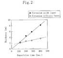
- FIG. 2is a graph illustrating relationship between deposition time for a zirconium oxide layer and the deposition thickness of a zirconium silicate layer in the semiconductor-device fabrication method in accordance with the first embodiment of the present invention.
- FIGS. 3 ( a ) and 3 ( b )are cross-sectional views illustrating process steps of a method for fabricating a semiconductor device in accordance with a second embodiment of the present invention.
- FIGS. 4 ( a ) through 4 ( e )are cross-sectional views illustrating process steps of a method for fabricating a semiconductor device in accordance with a third embodiment of the present invention.
- FIGS. 5 ( a ) and 5 ( b )are cross-sectional views illustrating process steps of a method for fabricating a semiconductor device in accordance with a fourth embodiment of the present invention.
- FIG. 6is a cross-sectional view illustrating a known semiconductor device.
- FIGS. 1 ( a ) through 1 ( c )are cross-sectional views illustrating process steps of a method for fabricating the semiconductor device in the first embodiment.
- the semiconductor device fabrication method in the first embodimentis characterized as follows: a metal silicate layer is formed on a silicon substrate, a metal oxide layer is also formed on the metal silicate layer, and the metal oxide layer is then removed, thereby forming a gate insulating film made of the metal silicate layer.
- a reactive sputtering methodfor example, is used to form the metal silicate layer and the metal oxide layer.
- an isolation 101is formed in, e.g., a p-type silicon substrate 100 by a known method.
- a metal target made of, e.g., zirconium (Zr)is then subjected to a reactive sputtering performed in a gaseous mixture of, e.g., Ar and O 2 gases, thereby depositing on the silicon substrate 100 a zirconium oxide layer (ZrO 2 layer) 102 with a thickness of, e.g., some 5 nm as a high-dielectric-constant material layer.
- a ternary compoundspecifically, ZrSi x O y , where x, y>0
- an O 2 plasma produced by the discharge generated during the sputtering processcauses the surface of the silicon substrate 100 and the surface of the metal target both to be oxidized.
- the zirconium oxide that has been formed on the metal target surfaceis then sputtered, such that the zirconium oxide is injected into the silicon oxide layer that has been formed on the silicon substrate 100 surface, and the zirconium oxide and the silicon oxide are mixed together. As a result, the zirconium silicate layer 103 is formed.
- the zirconium silicate layer 103 formed in this mannerhad a dielectric constant about twice as high as that of SiO 2 . This means that in the case of forming a zirconium silicate layer having an extremely small EOT of about 1.5 nm, the zirconium silicate layer may have a relatively large physical thickness of about 3 nm.
- the present inventorsalso found that, as shown in FIG. 2, the deposition thickness of the zirconium silicate layer 103 increased in proportion to the deposition time for the zirconium oxide layer 102 .
- the results shown in FIG. 2were obtained under the specific sputtering conditions that the pressure inside the chamber was 0.4 kPa, the discharge power was 200 W, and the Ar/O 2 flow rate ratio (which is a flow rate ratio per minute in a standard state) was 10/10 cc.
- the relationship between the deposition thickness of the zirconium oxide layer 102 and the deposition thickness of the zirconium silicate layer 103can be changed by altering the sputtering conditions.
- FIG. 2also indicates, for reference, the relationship between the deposition time for and deposition thickness of the zirconium oxide layer 102 .
- the zirconium oxide layer 102is removed with, e.g., a dilute hydrofluoric acid solution.
- the etch rate of the zirconium silicate layer 103being lower than that of the zirconium oxide layer 102 enables leaving only the zirconium silicate layer 103 .
- a gate insulating film 104made of the zirconium silicate layer 103 can be formed.
- a gate electrode 105is formed on the gate insulating film 104 .
- a sidewall insulating film 106is formed on both lateral faces of the gate electrode 105 ; and doped layers 107 , which act as source and drain regions, are defined on both sides of the gate electrode 105 in the silicon substrate 100 .
- An interlevel dielectric film 108is then formed over the silicon substrate 100 as well as over the gate electrode 105 and like members.
- a wire 109is formed on the interlevel dielectric film 108 . Note that the wire 109 has plugs that are formed in the interlevel dielectric film 108 so as to be connected to the doped layers 107 .
- the zirconium silicate layer 103is formed on the silicon substrate 100 , the zirconium oxide layer 102 is also formed on the zirconium silicate layer 103 , and the zirconium oxide layer 102 is then removed, thereby forming the gate insulating film 104 made of the zirconium silicate layer 103 .
- the zirconium silicate layer 103 with a uniform thickness and a dielectric constant higher than that of SiO 2can be formed by a reactive sputtering method in which a target made of zirconium is used, and the thickness of the zirconium silicate layer 103 can be easily and accurately adjusted by controlling the sputtering conditions. Accordingly, it is possible to obtain a gate insulating film 104 with small EOT and small leakage current, enabling realizing a low-power-consumption MOSFET having desired driving power.
- zirconiumis used as the material for the metal target in the first embodiment
- another material from which a compound (oxide) having a high dielectric constant (higher than the dielectric constant of SiO 2 ) can be obtained by reactive sputteringmay be used instead of zirconium.
- a metalsuch as Hf, Ti, Ta, Al, Pr, Nd or La, or any alloy of these metals may be used.
- the metal targetmay contain oxygen or a small quantity of silicon.
- the modified example of the first embodimentis different from the first embodiment in that a chemical vapor deposition method, instead of the reactive sputtering method, is used to form a zirconium silicate layer 103 and a zirconium oxide layer 102 in the process step shown in FIG. 1( a ).
- an oxide film(silicon oxide layer) having a thickness of about 1 nm is formed on the surface of a silicon substrate 100 in an H 2 O ambient at high temperature, in the initial stage of a chemical vapor deposition process. Then, a zirconium oxide layer 102 is formed over the silicon substrate 100 by a chemical vapor deposition method using a gaseous mixture of H 2 O and ZrCl 4 as a source gas.
- a reactionoccurs between the source gas containing zirconium and the silicon oxide layer, thereby forming a zirconium silicate layer 103 made of a ternary compound of zirconium, silicon and oxygen at the interface between the silicon substrate 100 and the zirconium oxide layer 102 .
- the zirconium silicate layer 103 formed in this mannerhas the same properties as in the case in which a reactive sputtering method is used (as in the first embodiment).
- the thickness configuration in the multilayer structure of the zirconium oxide layer 102 and the zirconium silicate layer 103can be established at will.
- the zirconium silicate layer 103is formed on the silicon substrate 100 , the zirconium oxide layer 102 is also formed on the zirconium silicate layer 103 , and the zirconium oxide layer 102 is then removed, thereby forming the gate insulating film 104 made of the zirconium silicate layer 103 .
- the zirconium silicate layer 103 with a uniform thickness and a dielectric constant higher than that of SiO 2can be formed by a chemical vapor deposition method using a source gas containing zirconium, and the thickness of the zirconium silicate layer 103 can be easily and accurately adjusted by controlling the deposition conditions. Accordingly, it is possible to obtain a gate insulating film 104 with small EOT and small leakage current, making a low-power-consumption MOSFET having desired driving power a reality.
- a source gas containing zirconium (Zr)is used in the modified example of the first embodiment, a source gas containing another material from which a compound (oxide) having a high dielectric constant can be obtained by a chemical vapor deposition method may be used instead.
- a source gas containing a metalsuch as Hf, Ti, Ta, Al, Pr, Nd or La, or any alloy of these metals may be used.
- a routine thermal CVD methodfor example, may be used, or an ALD (atomic layer deposition) process may also be used.
- ALDatomic layer deposition
- a metal oxide layersuch as a zirconium oxide layer is formed by depositing molecular strata one after another by pulsed (intermittent) supply of a source gas.
- Use of an ALD processcan serve to improve the controllability and uniformity of the thickness of a metal silicate layer such as a zirconium silicate layer.
- a reactive sputtering method or a chemical vapor deposition methodis used to form a metal silicate layer and a metal oxide layer in the first embodiment and the modified example of the first embodiment
- the present inventionis not limited thereto.
- any other film-forming method by which a high-quality metal silicate layer such as the zirconium silicate layer 103 can be formedmay be used.
- FIGS. 3 ( a ) and 3 ( b )are cross-sectional views illustrating process steps of a method for fabricating the semiconductor device in the second embodiment.
- the semiconductor device fabrication method in the second embodimentis characterized as follows: a metal silicate layer is formed on a silicon substrate, a metal oxide layer is also formed on the metal silicate layer, the metal oxide layer is then removed, and thereafter another metal oxide layer is formed, thereby forming a gate insulating film made of the metal silicate layer and said another metal oxide layer.
- a metal silicate layeris formed on a silicon substrate
- a metal oxide layeris also formed on the metal silicate layer
- the metal oxide layeris then removed, and thereafter another metal oxide layer is formed, thereby forming a gate insulating film made of the metal silicate layer and said another metal oxide layer.
- a zirconium silicate layer 103is formed on a silicon substrate 100 and a zirconium oxide layer 102 is also formed on the zirconium silicate layer 103 .
- the zirconium oxide layer 102is then removed in such a manner that only the zirconium silicate layer 103 is left.
- a gate insulating film 104(see FIG. 3( b )) composed of the zirconium silicate layer 103 and the hafnium oxide layer 110 in a multilayer structure can be formed.
- the dielectric constant of the hafnium oxide layer 110is higher than that of the zirconium oxide layer 102 .
- the multilayer structure of the zirconium silicate layer 103 and the hafnium oxide layer 110has a smaller EOT as compared to the multilayer structure of the zirconium silicate layer 103 and the zirconium oxide layer 102 when the multilayer structures have the same thickness.
- a gate electrode 105is formed on the gate insulating film 104 .
- a sidewall insulating film 106is formed on both lateral faces of the gate electrode 105 ; and doped layers 107 , which act as source and drain regions, are defined on both sides of the gate electrode 105 in the silicon substrate 100 .
- An interlevel dielectric film 108is then formed over the silicon substrate 100 as well as over the gate electrode 105 and like members.
- a wire 109is formed on the interlevel dielectric film 108 . Note that the wire 109 has plugs that are formed in the interlevel dielectric film 108 so as to be connected to the doped layers 107 .
- the zirconium silicate layer 103is formed on the silicon substrate 100 , the zirconium oxide layer 102 is also formed on the zirconium silicate layer 103 , the zirconium oxide layer 102 is then removed, and thereafter the hafnium oxide layer 110 is formed, thereby forming the gate insulating film 104 made of the zirconium silicate layer 103 and the hafnium oxide layer 110 .
- the use of a reactive sputtering method or a chemical vapor deposition methodenables the formation of a zirconium silicate layer 103 having a uniform thickness and a dielectric constant higher than the dielectric constant of SiO 2 , and the thickness of the zirconium silicate layer 103 can also be easily adjusted by controlling the sputtering conditions or the deposition conditions, for example. Further, since the hafnium oxide layer 110 is separately formed on the zirconium silicate layer 103 , the hafnium oxide layer 110 can be formed as designed without taking reaction with the silicon substrate 100 into account.
- the gate insulating film 104 with small EOT and small leakage currentcan be obtained, which enables realizing a low-power-consumption MOSFET having desired driving power.
- the multilayer structure of the zirconium silicate layer 103 and the hafnium oxide layer 110can be easily formed to have a desired thickness configuration.
- Thisenables the design of a gate insulating film 104 in accordance with the functions called for in a MOSFET. For example, designing a gate insulating film targeted at compatibility between high driving power and lower power consumption is facilitated.
- the zirconium silicate layer 103 and the zirconium oxide layer 102are preferably formed by a reactive sputtering method using a target made of zirconium or by a chemical vapor deposition method using a source gas containing zirconium. It is then ensured that the zirconium silicate layer 103 with a uniform thickness and a dielectric constant higher than that of SiO 2 can be formed, and the thickness of the zirconium oxide layer 102 can be accurately adjusted by controlling the sputtering conditions or the deposition conditions.
- a conventional thermal CVD method or an ALD processmay be used as the chemical vapor deposition method.
- the controllability and uniformity of the thickness of the zirconium silicate layer 103can be improved. Further, it goes without saying that any other film-forming method by which a zirconium silicate layer 103 of quality can be formed may be used instead of the reactive sputtering method or the chemical vapor deposition method.
- the zirconium silicate layer 103is used as the metal silicate layer functioning as the lower layer of the gate insulating film 104 in the second embodiment, the present invention is not limited thereto.
- the metal silicate layerpreferably contains a metal such as Zr, Hf, Ti, Al, Pr, Nd or La, or any alloy of these metals. It is then ensured that the dielectric constant of the metal silicate layer is higher than the dielectric constant of SiO 2 .
- hafnium oxide layer 110is used as said another metal oxide layer functioning as the upper layer of the gate insulating film 104 in the second embodiment, the present invention is not limited thereto.
- Said another metal oxide layerpreferably contains a metal such as Zr, Hf, Ti, Al, Pr, Nd or La, or any alloy of these metals. It should be noted, however, that a metal contained in the metal silicate layer that serves as the lower layer of the gate insulating film 104 is preferably different from a metal contained in said another metal oxide layer.
- a metal contained in the metal silicate layer functioning as the lower layer of the gate insulating film 104is preferably selected in such a manner that the metal silicate layer is thermally stable at the interface with the substrate and does not cause creation of great strain in the silicon crystal, which would result in deterioration of mobility in the silicon crystal.
- a metal contained in said another metal oxide layer functioning as the upper layer of the gate insulating film 104is preferably selected in such a manner that the dielectric constant of said another metal oxide layer is higher than the dielectric constant of the metal oxide layer containing the same kind of metal that the metal silicate layer contains.
- FIGS. 4 ( a ) through 4 ( e )are cross-sectional views illustrating process steps of a method for fabricating the semiconductor device in the third embodiment.
- the semiconductor device fabrication method in the third embodimentis characterized as follows: a metal silicate layer is formed on a silicon substrate, a metal oxide layer is also formed on the metal silicate layer, and the metal oxide layer is then partially removed, thereby forming a first gate insulating film made of the metal silicate layer, and a second gate insulating film made of the metal silicate layer and the metal oxide layer.
- a reactive sputtering methodfor example, is used to form the metal silicate layer and the metal oxide layer.
- an isolation 201is formed in, e.g., a p-type silicon substrate 200 by a known method, thereby defining a first device-formation region R A and a second device-formation region R B .
- a metal target made of, e.g., zirconium (Zr)is then subjected to a reactive sputtering performed in a gaseous mixture of, e.g., Ar and O 2 gases, thereby depositing, as a high-dielectric-constant material layer, a zirconium oxide layer (ZrO 2 layer) 202 with a thickness of, e.g., some 5 nm over the first device-formation region R A and the second device-formation region R B .
- a reactive sputteringperformed in a gaseous mixture of, e.g., Ar and O 2 gases, thereby depositing, as a high-dielectric-constant material layer, a zirconium oxide layer (ZrO 2 layer) 202 with a thickness of, e.g., some 5 nm over the first device-formation region R A and the second device-formation region R B .
- a ternary compoundspecifically, ZrSi x O y , where x, y>0
- a resist pattern 250is formed on part of the zirconium oxide layer 202 located in the second device-formation region R B .
- part of the zirconium oxide layer 202 located in the first device-formation region R Ais removed with, e.g., a dilute hydrofluoric acid solution.
- the etch rate of the zirconium silicate layer 203being lower than that of the zirconium oxide layer 202 enables leaving only the zirconium silicate layer 203 in the first device-formation region R A .
- a first gate insulating film 204 Asee FIG.
- a second gate insulating film 204 Bmade of the zirconium silicate layer 203 and the zirconium oxide layer 202 can also be formed in the second device-formation region R B .
- a first gate electrode 205 Ais formed on the first gate insulating film 204 A and a second gate electrode 205 B is also formed on the second gate insulating film 204 B as shown in FIG. 4( e ).
- a first sidewall insulating film 206 Ais formed on both lateral faces of the first gate electrode 205 A, and a second sidewall insulating film 206 B is also formed on both lateral faces of the second gate electrode 205 B.
- first doped layers 207 Awhich act as source and drain regions, are defined on both sides of the first gate electrode 205 A in the silicon substrate 200
- second doped layers 207 Bwhich act as source and drain regions, are also defined on both sides of the second gate electrode 205 B in the silicon substrate 200 .
- An interlevel dielectric film 208is then formed over the silicon substrate 200 as well as over the first and second gate electrodes 205 A and 205 B and like members. Thereafter, a first wire 209 A and a second wire 209 B are formed on the interlevel dielectric film 208 .
- first wire 209 Ahas plugs that are formed in the interlevel dielectric film 208 so as to be connected to the first doped layers 207 A
- second wire 209 Bhas plugs that are formed in the interlevel dielectric film 208 so as to be connected to the second doped layers 207 B.
- the zirconium silicate layer 203is formed on the silicon substrate 200 , the zirconium oxide layer 202 is also formed on the zirconium silicate layer 203 , and the zirconium oxide layer 202 is partially removed, thereby forming the first gate insulating film 204 A made of the zirconium silicate layer 203 , and the second gate insulating film 204 B made of the zirconium silicate layer 203 and the zirconium oxide layer 202 .
- the third embodimentis multi-gate insulating film technology in which the single layer structure of the zirconium silicate layer 203 is used as a thin gate insulting film, and the multilayer structure of the zirconium silicate layer 203 and the zirconium oxide layer 202 is used as a thick gate insulating film. Also, in the third embodiment, it is ensured that the zirconium silicate layer 203 with a uniform thickness and a dielectric constant higher than that of SiO 2 can be formed by a reactive sputtering method in which a target made of zirconium is used, and the thickness of the zirconium silicate layer 203 can be easily and accurately adjusted by controlling the sputtering conditions.
- the thin gate insulating film(the first gate insulating film 204 A)
- increase in the gate leakage currentcan be prevented when the multi-gate insulating film technology is used, enabling the formation of a low-power consumption system LSI.
- the first gate insulating film 204 Aenables realizing a MOSFET in which priority is given to increase in the driving power
- the second gate insulating film 204 Benables realizing a MOSFET in which priority is given to decrease in the consumption power.
- zirconiumis used as the material for the metal target in the third embodiment
- another material from which a compound (oxide) having a high dielectric constant (higher than the dielectric constant of SiO 2 ) can be obtained by reactive sputteringmay be used instead of zirconium.
- a metalsuch as Hf, Ti, Ta, Al, Pr, Nd or La, or any alloy of these metals may be used.
- the metal targetmay contain oxygen or a small quantity of silicon.
- a MOSFET including the first gate insulating film 204 Ais used in an internal circuit, while a MOSFET including the second gate insulating film 204 B is used in a peripheral circuit. This enables realizing a system LSI including a high-driving-power, low-power-consumption internal circuit and a low-power-consumption peripheral circuit.
- a MOSFET including the first gate insulating film 204 Ais used in a logic section, while a MOSFET including the second gate insulating film 204 B is used in a DRAM section. This enables realizing a system LSI including a high-driving-power, low-power-consumption logic section and a low-power-consumption DRAM section.
- the modified example of the third embodimentis different from the third embodiment in that a chemical vapor deposition method, instead of the reactive sputtering method, is used to form a zirconium silicate layer 203 and a zirconium oxide layer 202 in the process step shown in FIG. 4( a ).
- an oxide film(silicon oxide layer) having a thickness of about 1 nm is formed on the surface of a silicon substrate 200 in an H 2 O ambient at high temperature, in the initial stage of a chemical vapor deposition process.
- a zirconium oxide layer 202is formed over the silicon substrate 200 by a chemical vapor deposition method using a gaseous mixture of H 2 O and ZrCl 4 as a source gas.
- a reactionoccurs between the source gas containing zirconium and the silicon oxide layer, thereby forming a zirconium silicate layer 203 made of a ternary compound of zirconium, silicon and oxygen at the interface between the silicon substrate 200 and the zirconium oxide layer 202 .
- the zirconium silicate layer 203 formed in this mannerhas the same properties as in the case in which a reactive sputtering method is used (as in the third embodiment).
- the thickness configuration in the multilayer structure of the zirconium oxide layer 202 and the zirconium silicate layer 203can be established at will.
- the zirconium silicate layer 203is formed on the silicon substrate 200 , the zirconium oxide layer 202 is also formed on the zirconium silicate layer 203 , and the zirconium oxide layer 202 is then partially removed, thereby forming a first gate insulating film 204 A made of the zirconium silicate layer 203 , and a second gate insulating film 204 B made of the zirconium silicate layer 203 and the zirconium oxide layer 202 .
- the modified example of the third embodimentis multi-gate insulating film technology in which the single layer structure of the zirconium silicate layer 203 is used as a thin gate insulting film, and the multilayer structure of the zirconium silicate layer 203 and the zirconium oxide layer 202 is used as a thick gate insulating film.
- the zirconium silicate layer 203 with a uniform thickness and a dielectric constant higher than that of SiO 2can be formed by a chemical vapor deposition method using a source gas containing zirconium, and the thickness of the zirconium silicate layer 203 can be easily and accurately adjusted by controlling the deposition conditions.
- the thin gate insulating film(the first gate insulating film 204 A)
- increase in the gate leakage currentcan be prevented when the multi-gate insulating film technology is used, enabling the formation of a low-power consumption system LSI.
- the first gate insulating film 204 Aa MOSFET in which priority is given to increase in the driving power can be realized
- the second gate insulating film 204 Ba MOSFET in which priority is given to decrease in the consumption power can be realized. Consequently, a system LSI in which high driving power and low power consumption are compatible with each other can be realized.
- a source gas containing zirconium (Zr)is used in the modified example of the third embodiment
- a source gas containing another material from which a compound (oxide) having a high dielectric constant can be obtained by a chemical vapor deposition methodmay be used instead.
- a source gas containing a metalsuch as Hf, Ti, Ta, Al, Pr, Nd or La, or any alloy of these metals may be used.
- a routine thermal CVD methodfor example, may be used, or an ALD process may also be used.
- a metal oxide layersuch as a zirconium oxide layer is formed by depositing molecular strata one after another by pulsed supply of a source gas.
- Use of an ALD processcan serve to improve the controllability and uniformity in a metal silicate layer such as a zirconium silicate layer.
- a reactive sputtering method or a chemical vapor deposition methodis used to form a metal silicate layer and a metal oxide layer in the third embodiment and the modified example of the third embodiment
- the present inventionis not limited thereto.
- any other film-forming method by which a high-quality metal silicate layer such as the zirconium silicate layer 203 can be formedmay be used.
- FIGS. 5 ( a ) and 5 ( b )are cross-sectional views illustrating process steps of a method for fabricating the semiconductor device in the fourth embodiment.
- the semiconductor device fabrication method in the fourth embodimentis characterized as follows: a metal silicate layer is formed on a silicon substrate, a metal oxide layer is also formed on the metal silicate layer, the metal oxide layer is then partially removed, and thereafter another metal oxide layer is formed, thereby forming a first gate insulating film made of the metal silicate layer and said another metal oxide layer, and a second gate insulating film made of the metal silicate layer, the metal oxide layer and said another meal oxide layer.
- the same process steps as in the third embodiment or the modified example thereofare performed.
- a zirconium silicate layer 203is formed on a silicon substrate 200 , and a zirconium oxide layer 202 is also formed on the zirconium silicate layer 203 .
- the zirconium oxide layer 202is then removed in such a manner that only the zirconium silicate layer 203 is left in the first device-formation region R A , while the multilayer structure of the zirconium silicate layer 203 and the zirconium oxide layer 202 is left in the second device-formation region R B .
- a hafnium oxide layer (HfO 2 layer) 210 with a thickness of about 5 nmis formed as a high-dielectric-constant material layer over the entire surface of the silicon substrate 200 by, e.g., a reactive sputtering method.
- a first gate insulating film 204 A(see FIG. 5( b )) made of the multilayer structure of the zirconium silicate layer 203 and the hafnium oxide layer 210 can be formed in the first device-formation region R A
- a second gate insulating film 204 Bsee FIG.
- the multilayer structure of the zirconium silicate layer 203 and the hafnium oxide layer 210has a smaller EOT as compared to the multilayer structure of the zirconium silicate layer 203 and the zirconium oxide layer 202 when the multilayer structures have the same thickness.
- a first gate electrode 205 Ais formed on the first gate insulating film 204 A, and a second gate electrode 205 B is also formed on the second gate insulating film 204 B.
- a first sidewall insulating film 206 Ais formed on both lateral faces of the first gate electrode 205 A, and a second sidewall insulating film 206 B is also formed on both lateral faces of the second gate electrode 205 B.
- first doped layers 207 Awhich act as source and drain regions, are defined on both sides of the first gate electrode 205 A in the silicon substrate 200
- second doped layers 207 Bwhich act as source and drain regions, are also defined on both sides of the second gate electrode 205 B in the silicon substrate 200 .
- An interlevel dielectric film 208is then formed over the silicon substrate 200 as well as over the first and second gate electrodes 205 A and 205 B and like members. Thereafter, a first wire 209 A and a second wire 209 B are formed on the interlevel dielectric film 208 .
- first wire 209 Ahas plugs that are formed in the interlevel dielectric film 208 so as to be connected to the first doped layers 207 A
- second wire 209 Bhas plugs that are formed in the interlevel dielectric film 208 so as to be connected to the second doped layers 207 B.
- the zirconium silicate layer 203is formed on the silicon substrate 200 , the zirconium oxide layer 202 is also formed on the zirconium silicate layer 203 , the zirconium oxide layer 202 is then partially removed, and thereafter the hafnium oxide layer 210 is formed, thereby forming the first gate insulating film 204 A made of the zirconium silicate layer 203 and the hafnium oxide layer 210 , and the second gate insulating film 204 B made of the zirconium silicate layer 203 , the zirconium oxide layer 202 and the hafnium oxide layer 210 .
- the fourth embodimentis multi-gate insulating film technology in which the multilayer structure of the zirconium silicate layer 203 and the hafnium oxide layer 210 is used as a thin gate insulting film, and the multilayer structure of the zirconium silicate layer 203 , the zirconium oxide layer 202 and the hafnium oxide layer 210 is used as a thick gate insulating film.
- the zirconium silicate layer 203 with a uniform thickness and a dielectric constant higher than that of SiO 2can be formed using, e.g., a reactive sputtering method or a chemical vapor deposition method, and the thickness of the zirconium silicate layer 203 can be easily adjusted by controlling the sputtering conditions or the deposition conditions, for example.
- the hafnium oxide layer 210is separately formed on the zirconium silicate layer 203 or the zirconium oxide layer 202 , the hafnium oxide layer 210 can be formed as designed without taking reaction with the silicon substrate 200 into account.
- the multilayer structure of the zirconium silicate layer 203 and the hafnium oxide layer 210allows small EOT and small leakage current to be realized in the thin gate insulating film (the first gate insulating film 204 A), increase in the gate leakage current can be prevented when the multi-gate insulating film technology is used, enabling the formation of a low-power consumption system LSI.
- the first gate insulating film 204 Aa MOSFET in which priority is given to increase in the driving power can be realized
- the second gate insulating film 204 Ba MOSFET in which priority is given to decrease in the consumption power can be realized.
- a system LSI in which high driving power and low power consumption are compatible with each othercan be realized.
- the multilayer structure of the zirconium silicate layer 203 and the hafnium oxide layer 210can be easily formed to have a desired thickness configuration.
- Thisenables the design of a first gate insulating film 204 A or a second gate insulating film 204 B in accordance with the functions called for in a MOSFET. For example, designing a gate insulating film targeted at compatibility between high driving power and lower power consumption is facilitated.
- the zirconium silicate layer 203 and the zirconium oxide layer 202are formed by a reactive sputtering method using a target made of zirconium or by a chemical vapor deposition method using a source gas containing zirconium. It is then ensured that the zirconium silicate layer 203 with a uniform thickness and a dielectric constant higher than that of SiO 2 can be formed, and the thickness of the zirconium oxide layer 202 can be accurately adjusted by controlling the sputtering conditions or the deposition conditions. In this embodiment, a routine thermal CVD method or an ALD process, for example, may be used as the chemical vapor deposition method.
- any other film-forming method by which a high-quality zirconium silicate layer 203 can be formedmay be used instead of the reactive sputtering method or the chemical vapor deposition method.
- the zirconium silicate layer 203is used as the metal silicate layer functioning as the lower layer of the first or second gate insulating film 204 A or 204 B in the fourth embodiment, the present invention is not limited thereto.
- the metal silicate layerpreferably contains a metal such as Zr, Hf, Ti, Al, Pr, Nd or La, or any alloy of these metals. It is then ensured that the dielectric constant of the metal silicate layer is higher than that of SiO 2 .
- hafnium oxide layer 210is used as said another metal oxide layer functioning as the upper layer of the first or second gate insulating film 204 A or 204 B in the fourth embodiment, the present invention is not limited thereto.
- Said another metal oxide layerpreferably contains a metal such as Zr, Hf, Ti, Al, Pr, Nd or La, or any alloy of these metals. It should be noted, however, that a metal contained in the metal silicate layer that serves as the lower layer of the first or second gate insulating film 204 A or 204 B is preferably different from a metal contained in said another metal oxide layer.
- a metal contained in the metal silicate layer functioning as the lower layer of the first or second gate insulating film 204 A or 204 Bis preferably selected in such a manner that the metal silicate layer is thermally stable at the interface with the substrate and does not cause creation of great strain in the silicon crystal, which would result in deterioration of mobility in the silicon crystal.
- a metal contained in said another metal oxide layer functioning as the upper layer of the first or second gate insulating film 204 A or 204 Bis preferably selected in such a manner that the dielectric constant of said another metal oxide layer is higher than the dielectric constant of the metal oxide layer containing the same kind of metal that the metal silicate layer contains.
- a MOSFET including the first gate insulating film 204 Ais used in an internal circuit, while a MOSFET including the second gate insulating film 204 B is used in a peripheral circuit. It is then possible to realize a system LSI including a high-driving-power, low-power-consumption internal circuit and a low-power-consumption peripheral circuit.
- a MOSFET including the first gate insulating film 204 Ais used in a logic section, while a MOSFET including the second gate insulating film 204 B is used in a DRAM section. It is then possible to realize a system LSI including a high-driving-power, low-power-consumption logic section and a low-power-consumption DRAM section.
Landscapes
- Engineering & Computer Science (AREA)
- Physics & Mathematics (AREA)
- Condensed Matter Physics & Semiconductors (AREA)
- General Physics & Mathematics (AREA)
- Manufacturing & Machinery (AREA)
- Computer Hardware Design (AREA)
- Microelectronics & Electronic Packaging (AREA)
- Power Engineering (AREA)
- Chemical & Material Sciences (AREA)
- Chemical Kinetics & Catalysis (AREA)
- Crystallography & Structural Chemistry (AREA)
- General Chemical & Material Sciences (AREA)
- Optics & Photonics (AREA)
- Insulated Gate Type Field-Effect Transistor (AREA)
- Formation Of Insulating Films (AREA)
- Semiconductor Memories (AREA)
- Metal-Oxide And Bipolar Metal-Oxide Semiconductor Integrated Circuits (AREA)
- Thin Film Transistor (AREA)
Abstract
Description
- The present invention relates to semiconductor devices having gate insulating films made of a high dielectric constant material, and to methods for fabricating the same.[0001]
- With recent advances in techniques for enabling increased degrees of integration in and high-speed operation of semiconductor devices, MOSFETs (metal oxide semiconductor field effect transistors) have decreased in size. Along with this decrease in MOSFET size, gate insulating films have become progressively thinner, and as a result, the problem of enlarged gate leakage current due to tunnel current has become manifest. To address the problem, techniques have been studied for realizing a gate insulating film having a capacity equivalent to that of a thin SiO[0002]2film (that is, a small equivalent oxide (SiO2) thickness, hereinafter referred to as “EOT”) and having a large physical film thickness (meaning a small leakage current), by using, as a material for the gate insulating film, a high-k material having a dielectric constant higher than that of SiO2(hereinafter referred to as a “high-dielectric-constant material”). Specific examples of such a high-dielectric-constant material include an insulating metal oxide such as HfO2or ZrO2.
- In addition, lately, multi-function circuits, such as internal circuits for performing computational operations, peripheral circuits for carrying out input and output, and DRAMs (dynamic random access memories), have been generally integrated on a single chip set out as a system LSI. As components of such a system LSI, MOSFETs that, in accordance with their functions, have enhanced driving power even though their leakage current is large, or have decreased leakage current even though their driving power is low are being sought. Being used in this regard is technology by which the SiO[0003]2films that serve as gate insulating films in MOSFETs are varied in thickness on the basis of the MOSFET functions,—specifically, multi-gate insulating film technology for forming gate insulating films with differing thicknesses.
- When a high-dielectric-constant material is used as a material for a gate insulating film, however, it is difficult to obtain a desired EOT even though increase in the gate leakage current can be prevented.[0004]
- Further, there is also a problem with the multi-gate insulating film technology, in that the gate leakage current is increased owing to the small thickness of the gate insulating films.[0005]
- In view of the foregoing, a first object of the present invention is to realize a gate insulating film with small EOT and small leakage current, and a second object thereof is to prevent increase in gate leakage current when multi-gate insulating film technology is used.[0006]
- To achieve the objects, the present inventors investigated the cause of the failure to realize a desired EOT even when a high-dielectric-constant material (specifically, a metal oxide) is used as a material for a gate insulating film, and the following has been made clear.[0007]
- Specifically, when a metal oxide layer which serves as a gate insulating film is formed on a silicon substrate, an insulating compound layer (hereinafter, referred to as a “metal silicate layer) made of the three elements of silicon, oxygen and a metal contained in the metal oxide layer forms between the silicon substrate and the metal oxide layer. In other words, a gate insulating film is formed out of the multilayer structure of the metal silicate layer and the metal oxide layer. In this case, the dielectric constant of the metal silicate layer is lower than the dielectric constant of the metal oxide layer, thus decreasing the effective dielectric constant of the entire gate insulating film. As a result, a gate insulating film having a desired EOT cannot be formed, and therefore a MOSFET having such high driving power as expected cannot be realized, that is, the performance of the MOSFET cannot be enhanced.[0008]
- FIG. 6 is a cross-sectional view illustrating a known semiconductor device, specifically a known MOSFET in which zirconium oxide (ZrO[0009]2) is used as a highdielectric-constant material constituting a gate insulating film.
- As shown in FIG. 6, a[0010]
zirconium oxide layer 11, which serves as a gate insulating film, is formed on asilicon substrate 10. At this time, however, azirconium silicate layer 12 forms between thesilicon substrate 10 and thezirconium oxide layer 11. Accordingly, agate electrode 13 will be formed on the gate insulating film made of the multilayer structure of thezirconium oxide layer 11 and thezirconium silicate layer 12. - Meanwhile, the present inventors found that when a metal oxide layer, which acts as a high-dielectric-constant material layer, is formed on a silicon substrate by, e.g., reactive sputtering, a metal silicate layer having a uniform thickness of about 2 through 3 nm and having a dielectric constant higher than the dielectric constant of a SiO[0011]2film can be formed between the silicon substrate and the metal oxide layer by controlling particles sputtered from the target and implanted into the substrate surface, or by controlling the O2plasma generated during the sputtering. They also found that by using the metal silicate layer as a gate insulating film, that is, by forming the metal oxide layer and the metal silicate layer and subsequently removing the metal oxide layer, the first object can be achieved, that is, a gate insulating film with small EOT and small leakage current can be realized. Note that when chemical vapor deposition, for example, is used instead of the reactive sputtering to form a metal silicate layer, such a quality metal silicate layer as mentioned above can also be formed.
- The present inventors also found the following. When another metal oxide layer is formed on the metal silicate layer after the metal oxide layer has been removed, said another metal oxide layer can be formed as designed without taking reaction with the substrate into account; thus by using the multilayer structure of the metal silicate layer and said another metal oxide layer as a gate insulating film, the first object can also be achieved.[0012]
- The present inventors further found that by forming a metal oxide layer and a metal silicate layer, and then partially removing the metal oxide layer, multi-gate insulating film technology in which the single layer structure of the metal silicate layer is used as a thin gate insulating film and the multilayer structure of the metal silicate layer and the metal oxide layer is used as a thick gate insulating film can be realized. This enables the second object to be achieved, that is, the gate leakage current can be controlled when the multi-gate insulating film technology is used. In this case, the multilayer structure of the metal silicate layer and another metal oxide layer may also be used as a thin gate insulating film.[0013]
- The present invention was made based on the above-described findings. Specifically, in order to achieve the first object, a first inventive method for fabricating a semiconductor device includes the steps of: (a) forming a metal silicate layer containing at least a first metal on a silicon substrate, and also forming a metal oxide layer containing the first metal on the metal silicate layer; (b) removing the metal oxide layer, thereby forming a gate insulating film made of the metal silicate layer; and (c) forming a gate electrode on the gate insulating film.[0014]
- According to the first inventive method for fabricating a semiconductor device, a metal silicate layer and a metal oxide layer both containing a first metal are sequentially formed on a silicon substrate, and the metal oxide layer is then removed, thereby forming a gate insulating film made of the metal silicate layer. In this method, a metal silicate layer with a uniform thickness and a dielectric constant higher than that of SiO[0015]2can be formed by a reactive sputtering method or by a chemical vapor deposition method, for example, and the thickness of the metal silicate layer can be easily adjusted by controlling the sputtering conditions or the deposition conditions, for example. Accordingly, it is possible to obtain a gate insulating film with small EOT and small leakage current, enabling realizing a low-power-consumption MOSFET having desired driving power.
- In order to achieve the first object, a second inventive method for fabricating a semiconductor device includes the steps of: (a) forming a metal silicate layer containing at least a first metal on a silicon substrate, and also forming a metal oxide layer containing the first metal on the metal silicate layer; (b) removing the metal oxide layer, and then forming another metal oxide layer containing a second metal different from the first metal over the silicon substrate, thereby forming a gate insulating film made of the metal silicate layer and said another metal oxide layer; and (c) forming a gate electrode on the gate insulating film.[0016]
- According to the second inventive method for fabricating a semiconductor device, a metal silicate layer and a metal oxide layer both containing a first metal are sequentially formed on a silicon substrate, the metal oxide layer is then removed, and thereafter another metal oxide layer containing a second metal different form the first metal is formed, thereby forming a gate insulating film made of the metal silicate layer and said another metal oxide layer. In this method, a metal silicate layer with a uniform thickness and a dielectric constant higher than that of SiO[0017]2can be formed by a reactive sputtering method or by a chemical vapor deposition method, for example, and the thickness of the metal silicate layer can be easily adjusted by controlling the sputtering conditions or the deposition conditions, for example. Further, since said another metal oxide layer is separately formed on the metal silicate layer, said another metal oxide layer can be formed as designed without taking reaction with the silicon substrate into account. Accordingly, with the multilayer structure of the metal silicate layer and said another metal oxide layer, a gate insulating film with small EOT and small leakage current can be realized, which enables realizing a low-power-consumption MOSFET having desired driving power.
- Moreover, according to the second inventive method for fabricating a semiconductor device, the multilayer structure of the metal silicate layer and said another metal oxide layer can be easily formed to have a desired thickness configuration. This enables the design of a gate insulating film in accordance with the functions called for in a MOSFET. For example, designing a gate insulating film targeted at compatibility between high driving power and lower power consumption is facilitated.[0018]
- Furthermore, in the second inventive method for fabricating a semiconductor device, the first metal is preferably selected in such a manner that the metal silicate layer is thermally stable at the interface with the substrate and does not cause creation of great strain in the silicon crystal, which would result in deterioration of mobility in the silicon crystal. In addition, the second metal is preferably selected in such a manner that the dielectric constant of said another metal oxide layer containing the second metal is higher than the dielectric constant of the metal oxide layer containing the first metal.[0019]
- In order to achieve the second object, a third inventive method for fabricating a semiconductor device includes the steps of: (a) forming a metal silicate layer containing at least a first metal in a first device-formation region and a second device-formation region on a silicon substrate, and also forming a metal oxide layer containing the first metal on the metal silicate layer; (b) removing part of the metal oxide layer located in the first device-formation region, thereby forming a first gate insulating film made of the metal silicate layer in the first device-formation region, and also forming a second gate insulating film made of the metal silicate layer and the metal oxide layer in the second device-formation region; and (c) forming a first gate electrode on the first gate insulating film, and also forming a second gate electrode on the second gate insulating film.[0020]
- According to the third inventive method for fabricating a semiconductor device, a metal silicate layer and a metal oxide layer both containing a first metal are sequentially formed on a silicon substrate, and the metal oxide layer is then partially removed, thereby forming a first gate insulating film made of the metal silicate layer, and a second gate insulating film made of the metal silicate layer and the metal oxide layer. In other words, the third inventive method for fabricating a semiconductor device is multi-gate insulating film technology in which the single layer structure of the metal silicate layer is used as a thin gate insulting film, and the multilayer structure of the metal silicate layer and the metal oxide layer is used as a thick gate insulating film. Also, in the third inventive method for fabricating a semiconductor device, a metal silicate layer with a uniform thickness and a dielectric constant higher than that of SiO[0021]2can be formed by a reactive sputtering method or by a chemical vapor deposition method, for example, and the thickness of the metal silicate layer can be easily adjusted by controlling the sputtering conditions or the deposition conditions, for example. Accordingly, because small EOT and small leakage current can be realized in the thin gate insulating film (the first gate insulating film), increase in the gate leakage current can be prevented when the multi-gate insulating film technology is used, enabling the formation of a low-power consumption system LSI. Further, the first gate insulating film enables realizing a MOSFET in which priority is given to increase in the driving power, while the second gate insulating film enables realizing a MOSFET in which priority is given to decrease in the consumption power. As a result, a system LSI in which high driving power and low power consumption are compatible with each other can be realized.
- In order to achieve the second object, a fourth inventive method for fabricating a semiconductor device includes the steps of (a) forming a metal silicate layer containing at least a first metal in a first device-formation region and a second device-formation region on a silicon substrate, and also forming a metal oxide layer containing the first metal on the metal silicate layer; (b) removing part of the metal oxide layer located in the first device-formation region, and then forming another metal oxide layer containing a second metal different from the first metal over the first device-formation region and the second device-formation region, thereby forming in the first device-formation region a first gate insulating film made of the metal silicate layer and said another metal oxide layer, and also forming in the second device-formation region a second gate insulating film made of the metal silicate layer, the metal oxide layer and said another metal oxide layer; and (c) forming a first gate electrode on the first gate insulating film, and also forming a second gate electrode on the second gate insulating film.[0022]
- According to the fourth inventive method for fabricating a semiconductor device, a metal silicate layer and a metal oxide layer both containing a first metal are sequentially formed on a silicon substrate, the metal oxide layer is then partially removed, and thereafter another metal oxide layer containing a second metal different from the first metal is formed, thereby forming a first gate insulating film made of the metal silicate layer and said another metal oxide layer, and a second gate insulating film made of the metal silicate layer, the metal oxide layer and said another metal oxide layer. In other words, the fourth inventive method for fabricating a semiconductor device is multi-gate insulating film technology in which the multilayer structure of the metal silicate layer and said another metal oxide layer is used as a thin gate insulting film, and the multilayer structure of the metal silicate layer, the metal oxide layer and said another metal oxide layer is used as a thick gate insulating film. Also, in the fourth inventive method for fabricating a semiconductor device, a metal silicate layer with a uniform thickness and a dielectric constant higher than that of SiO[0023]2can be formed by a reactive sputtering method or by a chemical vapor deposition method, for example, and the thickness of the metal silicate layer can be easily adjusted by controlling the sputtering conditions or the deposition conditions, for example. Further, in the fourth inventive method for fabricating a semiconductor device, since said another metal oxide layer is separately formed on the metal silicate layer or the metal oxide layer, said another metal oxide layer can be formed as designed without taking reaction with the silicon substrate into account. Accordingly, because the multilayer structure of the metal silicate layer and said another metal oxide layer allows small EOT and small leakage current to be realized in the thin gate insulating film (the first gate insulating film), increase in the gate leakage current can be prevented when the multi-gate insulating film technology is used, enabling the formation of a low-power consumption system LSI. Further, with the first gate insulating film, a MOSFET in which priority is given to increase in the driving power can be realized, while with the second gate insulating film, a MOSFET in which priority is given to decrease in the consumption power can be realized. As a result, a system LSI in which high driving power and low power consumption are compatible with each other can be realized.
- Moreover, according to the fourth inventive method for fabricating a semiconductor device, the multilayer structure of the metal silicate layer and said another metal oxide layer, or the multilayer structure of the metal silicate layer, the metal oxide layer and said another metal oxide layer can be easily formed to have a desired thickness configuration. This enables the design of a gate insulating film in accordance with the functions called for in a MOSFET. For example, designing a gate insulating film targeted at compatibility between high driving power and lower power consumption is facilitated.[0024]
- Furthermore, in the fourth inventive method for fabricating a semiconductor device, the first metal is preferably selected in such a manner that the metal silicate layer is thermally stable at the interface with the substrate and does not cause creation of great strain in the silicon crystal, which would result in deterioration of mobility in the silicon crystal. In addition, the second metal is preferably selected in such a manner that the dielectric constant of said another metal oxide layer containing the second metal is higher than the dielectric constant of the metal oxide layer containing the first metal.[0025]
- In the first through fourth inventive methods for fabricating a semiconductor device, the step (a) preferably includes the step (d) of forming the metal silicate layer and the metal oxide layer by reactive sputtering in which a target containing at least the first metal is used.[0026]
- It is then ensured that a metal silicate layer with a uniform thickness and a dielectric constant higher than that of SiO[0027]2can be formed, and the thickness of the metal silicate layer can be accurately adjusted by controlling the sputtering conditions.
- In the first through fourth inventive methods for fabricating a semiconductor device, the step (a) preferably includes the step (e) of forming the metal silicate layer and the metal oxide layer by chemical vapor deposition in which a source gas containing at least the first metal is used.[0028]
- It is then ensured that a metal silicate layer with a uniform thickness and a dielectric constant higher than that of SiO[0029]2can be formed, and the thickness of the metal silicate layer can be accurately adjusted by controlling the deposition conditions.
- In this case, the step (e) preferably includes the step of forming the metal oxide layer in molecular strata deposited one after another by pulsed supply of the source gas.[0030]
- Then, the controllability and uniformity of the thickness of the metal silicate layer can be improved.[0031]
- In the first through fourth inventive methods for fabricating a semiconductor device, the first metal is preferably one metal among the group of metals consisting of Hf, Zr, Ti, Ta, Al, Pr, Nd and La, or an alloy made of two or more metals among the group of metals.[0032]
- This ensures that the dielectric constant of the metal silicate layer is higher than the dielectric constant of SiO[0033]2. Also, the first metal is particularly preferably Zr in the first or third inventive method for fabricating a semiconductor device, while in the second or fourth inventive method for fabricating a semiconductor device, the first metal is particularly preferably Zr and the second metal is particularly preferably Hf.
- In order to achieve the first object, a first inventive semiconductor device includes a MOSFET including a gate insulating film formed by sequentially stacking a metal silicate layer containing a first metal and a metal oxide layer containing a second metal different from the first metal.[0034]
- Specifically, the first inventive semiconductor device is that formed by the second inventive method for fabricating a semiconductor device. In the first inventive semiconductor device, a gate insulating film with small EOT and small leakage current can be realized, enabling realizing a low-power-consumption MOSFET having desired driving power. It is also possible to facilitate the design of a gate insulating film in accordance with the functions called for in a MOSFET.[0035]
- In order to achieve the second object, a second inventive semiconductor device includes a first MOSFET including a first gate insulating film made of a metal silicate layer containing a first metal, and a second MOSFET including a second gate insulating film formed by sequentially stacking the metal silicate layer and a metal oxide layer containing the first metal.[0036]
- Specifically, the second inventive semiconductor device is that formed by the third inventive method for fabricating a semiconductor device. In the second inventive semiconductor device, increase in the gate leakage current can be prevented when the multi-gate insulating film technology is used, enabling the formation of a low-power consumption system LSI. Further, priority can be given to increase in the driving power in the first MOSFET including the first gate insulating film, while priority can be given to decrease in the consumption power in the second MOSFET including the second gate insulating film. As a result, a system LSI in which high driving power and low power consumption are compatible with each other can be realized.[0037]
- In order to achieve the second object, a third inventive semiconductor device includes: a first MOSFET including a first gate insulating film formed by sequentially stacking a metal silicate layer containing a first metal and a metal oxide layer containing a second metal different from the first metal; and a second MOSFET including a second gate insulating film formed by sequentially stacking the metal silicate layer, a metal oxide layer containing the first metal, and the metal oxide layer containing the second metal.[0038]
- Specifically, the third inventive semiconductor device is that formed by the fourth inventive method for fabricating a semiconductor device. In the third inventive semiconductor device, increase in the gate leakage current can be prevented when the multi-gate insulating film technology is used, enabling the formation of a low-power consumption system LSI. Further, priority can be given to increase in the driving power in the first MOSFET including the first gate insulating film, while priority can be given to decrease in the consumption power in the second MOSFET including the second gate insulating film. As a result, a system LSI in which high driving power and low power consumption are compatible with each other can be realized. In addition, it is possible to facilitate the design of a gate insulating film in accordance with the functions called for in a MOSFET.[0039]
- In the first through third inventive semiconductor devices, the first metal is preferably one metal among the group of metals consisting of Hf, Zr, Ti, Ta, Al, Pr, Nd and La, or an alloy made of two or more metals among the group of metals.[0040]
- It is then ensured that the dielectric constant of the metal silicate layer is higher than the dielectric constant of SiO[0041]2.
- In the second or third inventive semiconductor device, the first MOSFET is preferably used in an internal circuit, while the second MOSFET is preferably used in a peripheral circuit.[0042]
- It is then possible to realize a system LSI including a high-driving-power, low-power-consumption internal circuit and a low-power-consumption peripheral circuit.[0043]
- In the second or third inventive semiconductor device, the first MOSFET is preferably used in a logic section, while the second MOSFET is preferably used in a DRAM section.[0044]
- It is then possible to realize a system LSI including a high-driving-power, low-power-consumption logic section and a low-power-consumption DRAM section.[0045]
- FIGS.[0046]1(a) through1(c) are cross-sectional views illustrating process steps of a method for fabricating a semiconductor device in accordance with a first embodiment of the present invention.
- FIG. 2 is a graph illustrating relationship between deposition time for a zirconium oxide layer and the deposition thickness of a zirconium silicate layer in the semiconductor-device fabrication method in accordance with the first embodiment of the present invention.[0047]
- FIGS.[0048]3(a) and3(b) are cross-sectional views illustrating process steps of a method for fabricating a semiconductor device in accordance with a second embodiment of the present invention.
- FIGS.[0049]4(a) through4(e) are cross-sectional views illustrating process steps of a method for fabricating a semiconductor device in accordance with a third embodiment of the present invention.
- FIGS.[0050]5(a) and5(b) are cross-sectional views illustrating process steps of a method for fabricating a semiconductor device in accordance with a fourth embodiment of the present invention.
- FIG. 6 is a cross-sectional view illustrating a known semiconductor device.[0051]
- First Embodiment[0052]
- Hereafter, taking an n-type MOSFET as an example, a semiconductor device in accordance with a first embodiment of the present invention and a method for fabricating the same will be described with reference to the accompanying drawings.[0053]
- FIGS.[0054]1(a) through1(c) are cross-sectional views illustrating process steps of a method for fabricating the semiconductor device in the first embodiment.
- The semiconductor device fabrication method in the first embodiment is characterized as follows: a metal silicate layer is formed on a silicon substrate, a metal oxide layer is also formed on the metal silicate layer, and the metal oxide layer is then removed, thereby forming a gate insulating film made of the metal silicate layer. In the first embodiment, a reactive sputtering method, for example, is used to form the metal silicate layer and the metal oxide layer.[0055]
- Specifically, as shown in FIG. 1([0056]a), an
isolation 101 is formed in, e.g., a p-type silicon substrate 100 by a known method. A metal target made of, e.g., zirconium (Zr) is then subjected to a reactive sputtering performed in a gaseous mixture of, e.g., Ar and O2gases, thereby depositing on the silicon substrate100 a zirconium oxide layer (ZrO2layer)102 with a thickness of, e.g., some 5 nm as a high-dielectric-constant material layer. At this time, azirconium silicate layer 103 made of a ternary compound (specifically, ZrSixOy, where x, y>0) of zirconium, silicon and oxygen, is formed at the interface between thesilicon substrate 100 and thezirconium oxide layer 102. - Hereafter, how the[0057]
zirconium silicate layer 103 is formed will be described in detail. First, an O2plasma produced by the discharge generated during the sputtering process causes the surface of thesilicon substrate 100 and the surface of the metal target both to be oxidized. The zirconium oxide that has been formed on the metal target surface is then sputtered, such that the zirconium oxide is injected into the silicon oxide layer that has been formed on thesilicon substrate 100 surface, and the zirconium oxide and the silicon oxide are mixed together. As a result, thezirconium silicate layer 103 is formed. - The present inventors found that the[0058]
zirconium silicate layer 103 formed in this manner had a dielectric constant about twice as high as that of SiO2. This means that in the case of forming a zirconium silicate layer having an extremely small EOT of about 1.5 nm, the zirconium silicate layer may have a relatively large physical thickness of about 3 nm. - The present inventors also found that, as shown in FIG. 2, the deposition thickness of the[0059]
zirconium silicate layer 103 increased in proportion to the deposition time for thezirconium oxide layer 102. The results shown in FIG. 2 were obtained under the specific sputtering conditions that the pressure inside the chamber was 0.4 kPa, the discharge power was 200 W, and the Ar/O2flow rate ratio (which is a flow rate ratio per minute in a standard state) was 10/10 cc. In other words, the relationship between the deposition thickness of thezirconium oxide layer 102 and the deposition thickness of thezirconium silicate layer 103 can be changed by altering the sputtering conditions. Needless to say, by thus changing the relationship, the thickness configuration in the multilayer structure of thezirconium oxide layer 102 and thezirconium silicate layer 103 can be established at will. FIG. 2 also indicates, for reference, the relationship between the deposition time for and deposition thickness of thezirconium oxide layer 102. - Next, as shown in FIG. 1([0060]b), the
zirconium oxide layer 102 is removed with, e.g., a dilute hydrofluoric acid solution. In this process step, the etch rate of thezirconium silicate layer 103 being lower than that of thezirconium oxide layer 102 enables leaving only thezirconium silicate layer 103. In this manner, a gate insulating film104 (see FIG. 1(c)) made of thezirconium silicate layer 103 can be formed. - Subsequently, as shown in FIG. 1([0061]c), a
gate electrode 105 is formed on thegate insulating film 104. Following this, asidewall insulating film 106 is formed on both lateral faces of thegate electrode 105; anddoped layers 107, which act as source and drain regions, are defined on both sides of thegate electrode 105 in thesilicon substrate 100. An interleveldielectric film 108 is then formed over thesilicon substrate 100 as well as over thegate electrode 105 and like members. Thereafter, awire 109 is formed on the interleveldielectric film 108. Note that thewire 109 has plugs that are formed in the interleveldielectric film 108 so as to be connected to the doped layers107. - As described above, according to the first embodiment, the[0062]
zirconium silicate layer 103 is formed on thesilicon substrate 100, thezirconium oxide layer 102 is also formed on thezirconium silicate layer 103, and thezirconium oxide layer 102 is then removed, thereby forming thegate insulating film 104 made of thezirconium silicate layer 103. In this embodiment, it is ensured that thezirconium silicate layer 103 with a uniform thickness and a dielectric constant higher than that of SiO2can be formed by a reactive sputtering method in which a target made of zirconium is used, and the thickness of thezirconium silicate layer 103 can be easily and accurately adjusted by controlling the sputtering conditions. Accordingly, it is possible to obtain agate insulating film 104 with small EOT and small leakage current, enabling realizing a low-power-consumption MOSFET having desired driving power. - It should be noted that although zirconium (Zr) is used as the material for the metal target in the first embodiment, another material from which a compound (oxide) having a high dielectric constant (higher than the dielectric constant of SiO[0063]2) can be obtained by reactive sputtering may be used instead of zirconium. For example, a metal such as Hf, Ti, Ta, Al, Pr, Nd or La, or any alloy of these metals may be used. In the first embodiment, the metal target may contain oxygen or a small quantity of silicon.
- Modified Example of First Embodiment[0064]
- Hereafter, taking an n-type MOSFET as an example, a method for fabricating a semiconductor device in accordance with a modified example of the first embodiment of the present invention will be described.[0065]
- The modified example of the first embodiment is different from the first embodiment in that a chemical vapor deposition method, instead of the reactive sputtering method, is used to form a[0066]
zirconium silicate layer 103 and azirconium oxide layer 102 in the process step shown in FIG. 1(a). - Specifically, after an[0067]
isolation 101 is formed, an oxide film (silicon oxide layer) having a thickness of about 1 nm is formed on the surface of asilicon substrate 100 in an H2O ambient at high temperature, in the initial stage of a chemical vapor deposition process. Then, azirconium oxide layer 102 is formed over thesilicon substrate 100 by a chemical vapor deposition method using a gaseous mixture of H2O and ZrCl4as a source gas. In this process step, a reaction occurs between the source gas containing zirconium and the silicon oxide layer, thereby forming azirconium silicate layer 103 made of a ternary compound of zirconium, silicon and oxygen at the interface between thesilicon substrate 100 and thezirconium oxide layer 102. Thezirconium silicate layer 103 formed in this manner has the same properties as in the case in which a reactive sputtering method is used (as in the first embodiment). Also, by changing the deposition conditions, such as the flow-rate ratio of the gaseous components included in the source gas, or the deposition temperature or the deposition time, the thickness configuration in the multilayer structure of thezirconium oxide layer 102 and thezirconium silicate layer 103 can be established at will. - Therefore, according to the modified example of the first embodiment, the same effects as in the first embodiment can be obtained.[0068]
- Specifically, in accordance with the modified example of the first embodiment, the[0069]
zirconium silicate layer 103 is formed on thesilicon substrate 100, thezirconium oxide layer 102 is also formed on thezirconium silicate layer 103, and thezirconium oxide layer 102 is then removed, thereby forming thegate insulating film 104 made of thezirconium silicate layer 103. In this modified example, it is ensured that thezirconium silicate layer 103 with a uniform thickness and a dielectric constant higher than that of SiO2can be formed by a chemical vapor deposition method using a source gas containing zirconium, and the thickness of thezirconium silicate layer 103 can be easily and accurately adjusted by controlling the deposition conditions. Accordingly, it is possible to obtain agate insulating film 104 with small EOT and small leakage current, making a low-power-consumption MOSFET having desired driving power a reality. - It should be noted that although the source gas containing zirconium (Zr) is used in the modified example of the first embodiment, a source gas containing another material from which a compound (oxide) having a high dielectric constant can be obtained by a chemical vapor deposition method may be used instead. For example, a source gas containing a metal such as Hf, Ti, Ta, Al, Pr, Nd or La, or any alloy of these metals may be used.[0070]
- Further, as the chemical vapor deposition method in the modified example of the first embodiment, a routine thermal CVD method, for example, may be used, or an ALD (atomic layer deposition) process may also be used. In an ALD process, a metal oxide layer such as a zirconium oxide layer is formed by depositing molecular strata one after another by pulsed (intermittent) supply of a source gas. (See, for example, pp. 46-47 in “2000 Symposium on VLSI Technology: Digest of Technical Papers” by Dae-Gyu Park, et al.; or pp. 2207-2209 in “2000 American Institute of Physics” by Dae-Gyu Park, et al.) Use of an ALD process can serve to improve the controllability and uniformity of the thickness of a metal silicate layer such as a zirconium silicate layer.[0071]
- Further, although a reactive sputtering method or a chemical vapor deposition method is used to form a metal silicate layer and a metal oxide layer in the first embodiment and the modified example of the first embodiment, the present invention is not limited thereto. Needless to say, any other film-forming method by which a high-quality metal silicate layer such as the[0072]
zirconium silicate layer 103 can be formed may be used. - Second Embodiment[0073]
- Hereafter, taking an n-type MOSFET as an example, a semiconductor device in accordance with a second embodiment of the present invention and a method for fabricating the same will be described with reference to the accompanying drawings.[0074]
- FIGS.[0075]3(a) and3(b) are cross-sectional views illustrating process steps of a method for fabricating the semiconductor device in the second embodiment.
- The semiconductor device fabrication method in the second embodiment is characterized as follows: a metal silicate layer is formed on a silicon substrate, a metal oxide layer is also formed on the metal silicate layer, the metal oxide layer is then removed, and thereafter another metal oxide layer is formed, thereby forming a gate insulating film made of the metal silicate layer and said another metal oxide layer. In the second embodiment, until the process step shown in FIG. 1([0076]b), the same process steps as in the first embodiment or the modified example thereof are performed.
- Specifically, as shown in FIGS.[0077]1(a) and1(b), by a reactive sputtering method or a chemical vapor deposition method, a
zirconium silicate layer 103 is formed on asilicon substrate 100 and azirconium oxide layer 102 is also formed on thezirconium silicate layer 103. Thezirconium oxide layer 102 is then removed in such a manner that only thezirconium silicate layer 103 is left. - Next, as shown in FIG. 3([0078]a), a hafnium oxide layer (HfO2layer)110 with a thickness of about 5 nm, which acts as a high-dielectric-constant material layer, is formed on the
zirconium silicate layer 103 by, e.g., a reactive sputtering method. In this way, a gate insulating film104 (see FIG. 3(b)) composed of thezirconium silicate layer 103 and thehafnium oxide layer 110 in a multilayer structure can be formed. The dielectric constant of thehafnium oxide layer 110 is higher than that of thezirconium oxide layer 102. Thus, the multilayer structure of thezirconium silicate layer 103 and thehafnium oxide layer 110 has a smaller EOT as compared to the multilayer structure of thezirconium silicate layer 103 and thezirconium oxide layer 102 when the multilayer structures have the same thickness. - Next, as shown in FIG. 3([0079]b), a
gate electrode 105 is formed on thegate insulating film 104. Thereafter, asidewall insulating film 106 is formed on both lateral faces of thegate electrode 105; anddoped layers 107, which act as source and drain regions, are defined on both sides of thegate electrode 105 in thesilicon substrate 100. An interleveldielectric film 108 is then formed over thesilicon substrate 100 as well as over thegate electrode 105 and like members. Thereafter, awire 109 is formed on the interleveldielectric film 108. Note that thewire 109 has plugs that are formed in the interleveldielectric film 108 so as to be connected to the doped layers107. - As described above, according to the second embodiment, the[0080]
zirconium silicate layer 103 is formed on thesilicon substrate 100, thezirconium oxide layer 102 is also formed on thezirconium silicate layer 103, thezirconium oxide layer 102 is then removed, and thereafter thehafnium oxide layer 110 is formed, thereby forming thegate insulating film 104 made of thezirconium silicate layer 103 and thehafnium oxide layer 110. In this embodiment, the use of a reactive sputtering method or a chemical vapor deposition method, for example, enables the formation of azirconium silicate layer 103 having a uniform thickness and a dielectric constant higher than the dielectric constant of SiO2, and the thickness of thezirconium silicate layer 103 can also be easily adjusted by controlling the sputtering conditions or the deposition conditions, for example. Further, since thehafnium oxide layer 110 is separately formed on thezirconium silicate layer 103, thehafnium oxide layer 110 can be formed as designed without taking reaction with thesilicon substrate 100 into account. Accordingly, with the multilayer structure of thezirconium silicate layer 103 and thehafnium oxide layer 110, thegate insulating film 104 with small EOT and small leakage current can be obtained, which enables realizing a low-power-consumption MOSFET having desired driving power. - Moreover, according to the second embodiment, the multilayer structure of the[0081]
zirconium silicate layer 103 and thehafnium oxide layer 110 can be easily formed to have a desired thickness configuration. This enables the design of agate insulating film 104 in accordance with the functions called for in a MOSFET. For example, designing a gate insulating film targeted at compatibility between high driving power and lower power consumption is facilitated. - It should be noted that in the second embodiment, the[0082]
zirconium silicate layer 103 and thezirconium oxide layer 102 are preferably formed by a reactive sputtering method using a target made of zirconium or by a chemical vapor deposition method using a source gas containing zirconium. It is then ensured that thezirconium silicate layer 103 with a uniform thickness and a dielectric constant higher than that of SiO2can be formed, and the thickness of thezirconium oxide layer 102 can be accurately adjusted by controlling the sputtering conditions or the deposition conditions. In the second embodiment, a conventional thermal CVD method or an ALD process, for example, may be used as the chemical vapor deposition method. In the case in which an ALD process is employed, the controllability and uniformity of the thickness of thezirconium silicate layer 103 can be improved. Further, it goes without saying that any other film-forming method by which azirconium silicate layer 103 of quality can be formed may be used instead of the reactive sputtering method or the chemical vapor deposition method. - It should be noted that although the[0083]
zirconium silicate layer 103 is used as the metal silicate layer functioning as the lower layer of thegate insulating film 104 in the second embodiment, the present invention is not limited thereto. The metal silicate layer preferably contains a metal such as Zr, Hf, Ti, Al, Pr, Nd or La, or any alloy of these metals. It is then ensured that the dielectric constant of the metal silicate layer is higher than the dielectric constant of SiO2. - Further, although the[0084]
hafnium oxide layer 110 is used as said another metal oxide layer functioning as the upper layer of thegate insulating film 104 in the second embodiment, the present invention is not limited thereto. Said another metal oxide layer preferably contains a metal such as Zr, Hf, Ti, Al, Pr, Nd or La, or any alloy of these metals. It should be noted, however, that a metal contained in the metal silicate layer that serves as the lower layer of thegate insulating film 104 is preferably different from a metal contained in said another metal oxide layer. - Furthermore, a metal contained in the metal silicate layer functioning as the lower layer of the[0085]
gate insulating film 104 is preferably selected in such a manner that the metal silicate layer is thermally stable at the interface with the substrate and does not cause creation of great strain in the silicon crystal, which would result in deterioration of mobility in the silicon crystal. In addition, a metal contained in said another metal oxide layer functioning as the upper layer of thegate insulating film 104 is preferably selected in such a manner that the dielectric constant of said another metal oxide layer is higher than the dielectric constant of the metal oxide layer containing the same kind of metal that the metal silicate layer contains. - Third Embodiment[0086]
- Hereafter, taking an n-type MOSFET as an example, a semiconductor device in accordance with a third embodiment of the present invention and a method for fabricating the same will be described with reference to the accompanying drawings.[0087]
- FIGS.[0088]4(a) through4(e) are cross-sectional views illustrating process steps of a method for fabricating the semiconductor device in the third embodiment.
- The semiconductor device fabrication method in the third embodiment is characterized as follows: a metal silicate layer is formed on a silicon substrate, a metal oxide layer is also formed on the metal silicate layer, and the metal oxide layer is then partially removed, thereby forming a first gate insulating film made of the metal silicate layer, and a second gate insulating film made of the metal silicate layer and the metal oxide layer. In the third embodiment, a reactive sputtering method, for example, is used to form the metal silicate layer and the metal oxide layer.[0089]
- Specifically, as shown in FIG. 4([0090]a), an
isolation 201 is formed in, e.g., a p-type silicon substrate 200 by a known method, thereby defining a first device-formation region RAand a second device-formation region RB. A metal target made of, e.g., zirconium (Zr) is then subjected to a reactive sputtering performed in a gaseous mixture of, e.g., Ar and O2gases, thereby depositing, as a high-dielectric-constant material layer, a zirconium oxide layer (ZrO2layer)202 with a thickness of, e.g., some 5 nm over the first device-formation region RAand the second device-formation region RB. At this time, azirconium silicate layer 203 made of a ternary compound (specifically, ZrSixOy, where x, y>0) of zirconium, silicon and oxygen, is formed at the interface between thesilicon substrate 200 and thezirconium oxide layer 202. Note that the specific process steps for forming, and the characteristics of thezirconium silicate layer 203 are the same with thezirconium silicate layer 103 in the first embodiment. - Next, as shown in FIG. 4([0091]b), a resist
pattern 250 is formed on part of thezirconium oxide layer 202 located in the second device-formation region RB. Thereafter, as shown in FIG. 4(c), using the resistpattern 250 as a mask, part of thezirconium oxide layer 202 located in the first device-formation region RAis removed with, e.g., a dilute hydrofluoric acid solution. In this process step, the etch rate of thezirconium silicate layer 203 being lower than that of thezirconium oxide layer 202 enables leaving only thezirconium silicate layer 203 in the first device-formation region RA. In this manner, a firstgate insulating film 204A (see FIG. 4(e)) made of thezirconium silicate layer 203 can be formed in the first device-formation region RA, and a secondgate insulating film 204B (see FIG. 4(e)) made of thezirconium silicate layer 203 and thezirconium oxide layer 202 can also be formed in the second device-formation region RB. - Subsequently, after the resist[0092]
pattern 250 is removed as shown in FIG. 4(d), afirst gate electrode 205A is formed on the firstgate insulating film 204A and asecond gate electrode 205B is also formed on the secondgate insulating film 204B as shown in FIG. 4(e). Following this, a firstsidewall insulating film 206A is formed on both lateral faces of thefirst gate electrode 205A, and a secondsidewall insulating film 206B is also formed on both lateral faces of thesecond gate electrode 205B. Further, firstdoped layers 207A, which act as source and drain regions, are defined on both sides of thefirst gate electrode 205A in thesilicon substrate 200, and seconddoped layers 207B, which act as source and drain regions, are also defined on both sides of thesecond gate electrode 205B in thesilicon substrate 200. An interleveldielectric film 208 is then formed over thesilicon substrate 200 as well as over the first andsecond gate electrodes first wire 209A and asecond wire 209B are formed on the interleveldielectric film 208. Note that thefirst wire 209A has plugs that are formed in the interleveldielectric film 208 so as to be connected to the firstdoped layers 207A, and thesecond wire 209B has plugs that are formed in the interleveldielectric film 208 so as to be connected to the seconddoped layers 207B. - As described above, according to the third embodiment, the[0093]
zirconium silicate layer 203 is formed on thesilicon substrate 200, thezirconium oxide layer 202 is also formed on thezirconium silicate layer 203, and thezirconium oxide layer 202 is partially removed, thereby forming the firstgate insulating film 204A made of thezirconium silicate layer 203, and the secondgate insulating film 204B made of thezirconium silicate layer 203 and thezirconium oxide layer 202. In other words, the third embodiment is multi-gate insulating film technology in which the single layer structure of thezirconium silicate layer 203 is used as a thin gate insulting film, and the multilayer structure of thezirconium silicate layer 203 and thezirconium oxide layer 202 is used as a thick gate insulating film. Also, in the third embodiment, it is ensured that thezirconium silicate layer 203 with a uniform thickness and a dielectric constant higher than that of SiO2can be formed by a reactive sputtering method in which a target made of zirconium is used, and the thickness of thezirconium silicate layer 203 can be easily and accurately adjusted by controlling the sputtering conditions. Accordingly, because small EOT and small leakage current can be realized in the thin gate insulating film (the firstgate insulating film 204A), increase in the gate leakage current can be prevented when the multi-gate insulating film technology is used, enabling the formation of a low-power consumption system LSI. Further, the firstgate insulating film 204A enables realizing a MOSFET in which priority is given to increase in the driving power, while the secondgate insulating film 204B enables realizing a MOSFET in which priority is given to decrease in the consumption power. As a result, a system LSI in which high driving power and low power consumption are compatible with each other can be realized. - It should be noted that although zirconium (Zr) is used as the material for the metal target in the third embodiment, another material from which a compound (oxide) having a high dielectric constant (higher than the dielectric constant of SiO[0094]2) can be obtained by reactive sputtering may be used instead of zirconium. For example, a metal such as Hf, Ti, Ta, Al, Pr, Nd or La, or any alloy of these metals may be used. In the third embodiment, the metal target may contain oxygen or a small quantity of silicon.
- In addition, in the third embodiment, it is preferable that a MOSFET including the first[0095]
gate insulating film 204A is used in an internal circuit, while a MOSFET including the secondgate insulating film 204B is used in a peripheral circuit. This enables realizing a system LSI including a high-driving-power, low-power-consumption internal circuit and a low-power-consumption peripheral circuit. - Furthermore, in the third embodiment, it is preferable that a MOSFET including the first[0096]
gate insulating film 204A is used in a logic section, while a MOSFET including the secondgate insulating film 204B is used in a DRAM section. This enables realizing a system LSI including a high-driving-power, low-power-consumption logic section and a low-power-consumption DRAM section. - Modified Example of Third Embodiment[0097]
- Hereafter, taking an n-type MOSFET as an example, a method for fabricating a semiconductor device in accordance with a modified example of the third embodiment of the present invention will be described.[0098]
- The modified example of the third embodiment is different from the third embodiment in that a chemical vapor deposition method, instead of the reactive sputtering method, is used to form a[0099]
zirconium silicate layer 203 and azirconium oxide layer 202 in the process step shown in FIG. 4(a). - Specifically, after an[0100]
isolation 201 is formed, an oxide film (silicon oxide layer) having a thickness of about 1 nm is formed on the surface of asilicon substrate 200 in an H2O ambient at high temperature, in the initial stage of a chemical vapor deposition process. Then, azirconium oxide layer 202 is formed over thesilicon substrate 200 by a chemical vapor deposition method using a gaseous mixture of H2O and ZrCl4as a source gas. In this process step, a reaction occurs between the source gas containing zirconium and the silicon oxide layer, thereby forming azirconium silicate layer 203 made of a ternary compound of zirconium, silicon and oxygen at the interface between thesilicon substrate 200 and thezirconium oxide layer 202. Thezirconium silicate layer 203 formed in this manner has the same properties as in the case in which a reactive sputtering method is used (as in the third embodiment). Also, by changing the deposition conditions, such as the flow-rate ratio of the gaseous components included in the source gas, or the deposition temperature or the deposition time, the thickness configuration in the multilayer structure of thezirconium oxide layer 202 and thezirconium silicate layer 203 can be established at will. - Therefore, according to the modified example of the third embodiment, the same effects as in the third embodiment can be obtained.[0101]
- Specifically, in accordance with the modified example of the third embodiment, the[0102]
zirconium silicate layer 203 is formed on thesilicon substrate 200, thezirconium oxide layer 202 is also formed on thezirconium silicate layer 203, and thezirconium oxide layer 202 is then partially removed, thereby forming a firstgate insulating film 204A made of thezirconium silicate layer 203, and a secondgate insulating film 204B made of thezirconium silicate layer 203 and thezirconium oxide layer 202. In other words, the modified example of the third embodiment is multi-gate insulating film technology in which the single layer structure of thezirconium silicate layer 203 is used as a thin gate insulting film, and the multilayer structure of thezirconium silicate layer 203 and thezirconium oxide layer 202 is used as a thick gate insulating film. In the modified example of the third embodiment, it is ensured that thezirconium silicate layer 203 with a uniform thickness and a dielectric constant higher than that of SiO2can be formed by a chemical vapor deposition method using a source gas containing zirconium, and the thickness of thezirconium silicate layer 203 can be easily and accurately adjusted by controlling the deposition conditions. Accordingly, because small EOT and small leakage current can be realized in the thin gate insulating film (the firstgate insulating film 204A), increase in the gate leakage current can be prevented when the multi-gate insulating film technology is used, enabling the formation of a low-power consumption system LSI. Further, with the firstgate insulating film 204A, a MOSFET in which priority is given to increase in the driving power can be realized, while with the secondgate insulating film 204B, a MOSFET in which priority is given to decrease in the consumption power can be realized. Consequently, a system LSI in which high driving power and low power consumption are compatible with each other can be realized. - It should be noted that although the source gas containing zirconium (Zr) is used in the modified example of the third embodiment, a source gas containing another material from which a compound (oxide) having a high dielectric constant can be obtained by a chemical vapor deposition method may be used instead. For example, a source gas containing a metal such as Hf, Ti, Ta, Al, Pr, Nd or La, or any alloy of these metals may be used.[0103]
- Further, as the chemical vapor deposition method in the modified example of the third embodiment, a routine thermal CVD method, for example, may be used, or an ALD process may also be used. In an ALD process, a metal oxide layer such as a zirconium oxide layer is formed by depositing molecular strata one after another by pulsed supply of a source gas. Use of an ALD process can serve to improve the controllability and uniformity in a metal silicate layer such as a zirconium silicate layer.[0104]
- Further, although a reactive sputtering method or a chemical vapor deposition method is used to form a metal silicate layer and a metal oxide layer in the third embodiment and the modified example of the third embodiment, the present invention is not limited thereto. Needless to say, any other film-forming method by which a high-quality metal silicate layer such as the[0105]
zirconium silicate layer 203 can be formed may be used. - Fourth Embodiment[0106]
- Hereafter, taking an n-type MOSFET as an example, a semiconductor device in accordance with a fourth embodiment of the present invention and a method for fabricating the same will be described with reference to the accompanying drawings.[0107]
- FIGS.[0108]5(a) and5(b) are cross-sectional views illustrating process steps of a method for fabricating the semiconductor device in the fourth embodiment.
- The semiconductor device fabrication method in the fourth embodiment is characterized as follows: a metal silicate layer is formed on a silicon substrate, a metal oxide layer is also formed on the metal silicate layer, the metal oxide layer is then partially removed, and thereafter another metal oxide layer is formed, thereby forming a first gate insulating film made of the metal silicate layer and said another metal oxide layer, and a second gate insulating film made of the metal silicate layer, the metal oxide layer and said another meal oxide layer. In the fourth embodiment, until the process step shown in FIG. 4([0109]d), the same process steps as in the third embodiment or the modified example thereof are performed.
- Specifically, as shown in FIGS.[0110]4(a) through4(d), by, e.g., a reactive sputtering method or a chemical vapor deposition method, a
zirconium silicate layer 203 is formed on asilicon substrate 200, and azirconium oxide layer 202 is also formed on thezirconium silicate layer 203. Thezirconium oxide layer 202 is then removed in such a manner that only thezirconium silicate layer 203 is left in the first device-formation region RA, while the multilayer structure of thezirconium silicate layer 203 and thezirconium oxide layer 202 is left in the second device-formation region RB. - Next, as shown in FIG. 5([0111]a), a hafnium oxide layer (HfO2layer)210 with a thickness of about 5 nm is formed as a high-dielectric-constant material layer over the entire surface of the
silicon substrate 200 by, e.g., a reactive sputtering method. In this manner, a firstgate insulating film 204A (see FIG. 5(b)) made of the multilayer structure of thezirconium silicate layer 203 and thehafnium oxide layer 210 can be formed in the first device-formation region RA, while a secondgate insulating film 204B (see FIG. 5(b)) made of the multilayer structure of thezirconium silicate layer 203, thezirconium oxide layer 202 and thehafnium oxide layer 210 can be formed in the second device-formation region RB. In this case, the dielectric constant of thehafnium oxide layer 210 is higher than that of thezirconium oxide layer 202. Thus, the multilayer structure of thezirconium silicate layer 203 and thehafnium oxide layer 210 has a smaller EOT as compared to the multilayer structure of thezirconium silicate layer 203 and thezirconium oxide layer 202 when the multilayer structures have the same thickness. - Next, as shown in FIG. 5([0112]b), a
first gate electrode 205A is formed on the firstgate insulating film 204A, and asecond gate electrode 205B is also formed on the secondgate insulating film 204B. Following this, a firstsidewall insulating film 206A is formed on both lateral faces of thefirst gate electrode 205A, and a secondsidewall insulating film 206B is also formed on both lateral faces of thesecond gate electrode 205B. Further, firstdoped layers 207A, which act as source and drain regions, are defined on both sides of thefirst gate electrode 205A in thesilicon substrate 200, and seconddoped layers 207B, which act as source and drain regions, are also defined on both sides of thesecond gate electrode 205B in thesilicon substrate 200. An interleveldielectric film 208 is then formed over thesilicon substrate 200 as well as over the first andsecond gate electrodes first wire 209A and asecond wire 209B are formed on the interleveldielectric film 208. Note that thefirst wire 209A has plugs that are formed in the interleveldielectric film 208 so as to be connected to the firstdoped layers 207A, while thesecond wire 209B has plugs that are formed in the interleveldielectric film 208 so as to be connected to the seconddoped layers 207B. - As described above, according to the fourth embodiment, the[0113]
zirconium silicate layer 203 is formed on thesilicon substrate 200, thezirconium oxide layer 202 is also formed on thezirconium silicate layer 203, thezirconium oxide layer 202 is then partially removed, and thereafter thehafnium oxide layer 210 is formed, thereby forming the firstgate insulating film 204A made of thezirconium silicate layer 203 and thehafnium oxide layer 210, and the secondgate insulating film 204B made of thezirconium silicate layer 203, thezirconium oxide layer 202 and thehafnium oxide layer 210. In other words, the fourth embodiment is multi-gate insulating film technology in which the multilayer structure of thezirconium silicate layer 203 and thehafnium oxide layer 210 is used as a thin gate insulting film, and the multilayer structure of thezirconium silicate layer 203, thezirconium oxide layer 202 and thehafnium oxide layer 210 is used as a thick gate insulating film. Also, in the fourth embodiment, it is ensured that thezirconium silicate layer 203 with a uniform thickness and a dielectric constant higher than that of SiO2can be formed using, e.g., a reactive sputtering method or a chemical vapor deposition method, and the thickness of thezirconium silicate layer 203 can be easily adjusted by controlling the sputtering conditions or the deposition conditions, for example. Further, since thehafnium oxide layer 210 is separately formed on thezirconium silicate layer 203 or thezirconium oxide layer 202, thehafnium oxide layer 210 can be formed as designed without taking reaction with thesilicon substrate 200 into account. Accordingly, because the multilayer structure of thezirconium silicate layer 203 and thehafnium oxide layer 210 allows small EOT and small leakage current to be realized in the thin gate insulating film (the firstgate insulating film 204A), increase in the gate leakage current can be prevented when the multi-gate insulating film technology is used, enabling the formation of a low-power consumption system LSI. Further, with the firstgate insulating film 204A, a MOSFET in which priority is given to increase in the driving power can be realized, while with the secondgate insulating film 204B, a MOSFET in which priority is given to decrease in the consumption power can be realized. As a result, a system LSI in which high driving power and low power consumption are compatible with each other can be realized. - Moreover, according to the fourth embodiment, the multilayer structure of the[0114]
zirconium silicate layer 203 and thehafnium oxide layer 210, or the multilayer structure of thezirconium silicate layer 203, thezirconium oxide layer 202 and thehafnium oxide layer 210 can be easily formed to have a desired thickness configuration. This enables the design of a firstgate insulating film 204A or a secondgate insulating film 204B in accordance with the functions called for in a MOSFET. For example, designing a gate insulating film targeted at compatibility between high driving power and lower power consumption is facilitated. - Note that it is preferable that the[0115]
zirconium silicate layer 203 and thezirconium oxide layer 202 are formed by a reactive sputtering method using a target made of zirconium or by a chemical vapor deposition method using a source gas containing zirconium. It is then ensured that thezirconium silicate layer 203 with a uniform thickness and a dielectric constant higher than that of SiO2can be formed, and the thickness of thezirconium oxide layer 202 can be accurately adjusted by controlling the sputtering conditions or the deposition conditions. In this embodiment, a routine thermal CVD method or an ALD process, for example, may be used as the chemical vapor deposition method. Use of an ALD process can serve to improve the controllability and uniformity of the thickness of thezirconium silicate layer 203. Needless to say, any other film-forming method by which a high-qualityzirconium silicate layer 203 can be formed may be used instead of the reactive sputtering method or the chemical vapor deposition method. - It should be noted that although the[0116]
zirconium silicate layer 203 is used as the metal silicate layer functioning as the lower layer of the first or secondgate insulating film - Further, although the[0117]
hafnium oxide layer 210 is used as said another metal oxide layer functioning as the upper layer of the first or secondgate insulating film gate insulating film - Furthermore, a metal contained in the metal silicate layer functioning as the lower layer of the first or second[0118]
gate insulating film gate insulating film - In addition, in the fourth embodiment, it is preferable that a MOSFET including the first[0119]
gate insulating film 204A is used in an internal circuit, while a MOSFET including the secondgate insulating film 204B is used in a peripheral circuit. It is then possible to realize a system LSI including a high-driving-power, low-power-consumption internal circuit and a low-power-consumption peripheral circuit. - Furthermore, in the fourth embodiment, it is preferable that a MOSFET including the first[0120]
gate insulating film 204A is used in a logic section, while a MOSFET including the secondgate insulating film 204B is used in a DRAM section. It is then possible to realize a system LSI including a high-driving-power, low-power-consumption logic section and a low-power-consumption DRAM section.
Claims (34)
Applications Claiming Priority (3)
| Application Number | Priority Date | Filing Date | Title |
|---|---|---|---|
| JP2001102908 | 2001-04-02 | ||
| JP2001-102908 | 2001-04-02 | ||
| PCT/JP2002/000997WO2002082554A1 (en) | 2001-04-02 | 2002-02-06 | Semiconductor device and method for manufacture thereof |
Publications (2)
| Publication Number | Publication Date |
|---|---|
| US20030173586A1true US20030173586A1 (en) | 2003-09-18 |
| US6812101B2 US6812101B2 (en) | 2004-11-02 |
Family
ID=18956046
Family Applications (1)
| Application Number | Title | Priority Date | Filing Date |
|---|---|---|---|
| US10/332,519Expired - LifetimeUS6812101B2 (en) | 2001-04-02 | 2002-02-06 | Semiconductor device and method for manufacture thereof |
Country Status (7)
| Country | Link |
|---|---|
| US (1) | US6812101B2 (en) |
| EP (2) | EP1677361A2 (en) |
| JP (1) | JP3730962B2 (en) |
| KR (1) | KR100500013B1 (en) |
| CN (1) | CN1310336C (en) |
| DE (1) | DE60220230T2 (en) |
| WO (1) | WO2002082554A1 (en) |
Cited By (70)
| Publication number | Priority date | Publication date | Assignee | Title |
|---|---|---|---|---|
| US20030172872A1 (en)* | 2002-01-25 | 2003-09-18 | Applied Materials, Inc. | Apparatus for cyclical deposition of thin films |
| US20030183870A1 (en)* | 2002-03-27 | 2003-10-02 | Fujitsu Limited | Semiconductor memory device and manufacturing method thereof |
| US20030232511A1 (en)* | 2002-06-14 | 2003-12-18 | Applied Materials, Inc. | ALD metal oxide deposition process using direct oxidation |
| US20030232506A1 (en)* | 2002-06-14 | 2003-12-18 | Applied Materials, Inc. | System and method for forming a gate dielectric |
| US20040077183A1 (en)* | 2002-06-04 | 2004-04-22 | Hua Chung | Titanium tantalum nitride silicide layer |
| US20040187304A1 (en)* | 2003-01-07 | 2004-09-30 | Applied Materials, Inc. | Enhancement of Cu line reliability using thin ALD TaN film to cap the Cu line |
| US20040224089A1 (en)* | 2002-10-18 | 2004-11-11 | Applied Materials, Inc. | Silicon-containing layer deposition with silicon compounds |
| US6831004B2 (en) | 2000-06-27 | 2004-12-14 | Applied Materials, Inc. | Formation of boride barrier layers using chemisorption techniques |
| US6838125B2 (en) | 2002-07-10 | 2005-01-04 | Applied Materials, Inc. | Method of film deposition using activated precursor gases |
| US6849545B2 (en) | 2001-06-20 | 2005-02-01 | Applied Materials, Inc. | System and method to form a composite film stack utilizing sequential deposition techniques |
| US6916398B2 (en) | 2001-10-26 | 2005-07-12 | Applied Materials, Inc. | Gas delivery apparatus and method for atomic layer deposition |
| US6936538B2 (en) | 2001-07-16 | 2005-08-30 | Applied Materials, Inc. | Method and apparatus for depositing tungsten after surface treatment to improve film characteristics |
| US6958296B2 (en) | 2001-05-07 | 2005-10-25 | Applied Materials, Inc. | CVD TiSiN barrier for copper integration |
| US20050253181A1 (en)* | 2004-05-14 | 2005-11-17 | Nec Electronics Corporation | Semiconductor device |
| US6972267B2 (en) | 2002-03-04 | 2005-12-06 | Applied Materials, Inc. | Sequential deposition of tantalum nitride using a tantalum-containing precursor and a nitrogen-containing precursor |
| US7049226B2 (en) | 2001-09-26 | 2006-05-23 | Applied Materials, Inc. | Integration of ALD tantalum nitride for copper metallization |
| US20060115934A1 (en)* | 2004-12-01 | 2006-06-01 | Yihwan Kim | Selective epitaxy process with alternating gas supply |
| US7081271B2 (en) | 2001-12-07 | 2006-07-25 | Applied Materials, Inc. | Cyclical deposition of refractory metal silicon nitride |
| US20060166414A1 (en)* | 2004-12-01 | 2006-07-27 | Carlson David K | Selective deposition |
| US20060187699A1 (en)* | 2003-03-17 | 2006-08-24 | Ronda Cornelis R | Semiconductor devcie with isolation layer |
| US20060234463A1 (en)* | 2005-04-14 | 2006-10-19 | Alejandro Avellan | Method for fabricating an electrical component |
| US7204886B2 (en) | 2002-11-14 | 2007-04-17 | Applied Materials, Inc. | Apparatus and method for hybrid chemical processing |
| US7211508B2 (en) | 2003-06-18 | 2007-05-01 | Applied Materials, Inc. | Atomic layer deposition of tantalum based barrier materials |
| US7220673B2 (en) | 2000-06-28 | 2007-05-22 | Applied Materials, Inc. | Method for depositing tungsten-containing layers by vapor deposition techniques |
| US7235492B2 (en) | 2005-01-31 | 2007-06-26 | Applied Materials, Inc. | Low temperature etchant for treatment of silicon-containing surfaces |
| US7241686B2 (en) | 2004-07-20 | 2007-07-10 | Applied Materials, Inc. | Atomic layer deposition of tantalum-containing materials using the tantalum precursor TAIMATA |
| US7244683B2 (en) | 2003-01-07 | 2007-07-17 | Applied Materials, Inc. | Integration of ALD/CVD barriers with porous low k materials |
| US7352048B2 (en) | 2001-09-26 | 2008-04-01 | Applied Materials, Inc. | Integration of barrier layer and seed layer |
| US7396565B2 (en)* | 2002-04-08 | 2008-07-08 | Applied Materials, Inc. | Multiple precursor cyclical deposition system |
| US7402534B2 (en) | 2005-08-26 | 2008-07-22 | Applied Materials, Inc. | Pretreatment processes within a batch ALD reactor |
| US7416979B2 (en) | 2001-07-25 | 2008-08-26 | Applied Materials, Inc. | Deposition methods for barrier and tungsten materials |
| US7429402B2 (en) | 2004-12-10 | 2008-09-30 | Applied Materials, Inc. | Ruthenium as an underlayer for tungsten film deposition |
| US7429516B2 (en) | 2002-02-26 | 2008-09-30 | Applied Materials, Inc. | Tungsten nitride atomic layer deposition processes |
| US7429361B2 (en) | 2002-07-17 | 2008-09-30 | Applied Materials, Inc. | Method and apparatus for providing precursor gas to a processing chamber |
| US7439191B2 (en) | 2002-04-05 | 2008-10-21 | Applied Materials, Inc. | Deposition of silicon layers for active matrix liquid crystal display (AMLCD) applications |
| US7465666B2 (en) | 2000-06-28 | 2008-12-16 | Applied Materials, Inc. | Method for forming tungsten materials during vapor deposition processes |
| US7470611B2 (en) | 1998-10-01 | 2008-12-30 | Applied Materials, Inc. | In situ deposition of a low K dielectric layer, barrier layer, etch stop, and anti-reflective coating for damascene application |
| US7473638B2 (en) | 2002-01-26 | 2009-01-06 | Applied Materials, Inc. | Plasma-enhanced cyclic layer deposition process for barrier layers |
| US7517775B2 (en) | 2003-10-10 | 2009-04-14 | Applied Materials, Inc. | Methods of selective deposition of heavily doped epitaxial SiGe |
| US7521379B2 (en) | 2006-10-09 | 2009-04-21 | Applied Materials, Inc. | Deposition and densification process for titanium nitride barrier layers |
| US7547952B2 (en) | 2003-04-04 | 2009-06-16 | Applied Materials, Inc. | Method for hafnium nitride deposition |
| US7585762B2 (en) | 2007-09-25 | 2009-09-08 | Applied Materials, Inc. | Vapor deposition processes for tantalum carbide nitride materials |
| US7588980B2 (en) | 2006-07-31 | 2009-09-15 | Applied Materials, Inc. | Methods of controlling morphology during epitaxial layer formation |
| US7611990B2 (en) | 2001-07-25 | 2009-11-03 | Applied Materials, Inc. | Deposition methods for barrier and tungsten materials |
| US7648927B2 (en) | 2005-06-21 | 2010-01-19 | Applied Materials, Inc. | Method for forming silicon-containing materials during a photoexcitation deposition process |
| US7651955B2 (en) | 2005-06-21 | 2010-01-26 | Applied Materials, Inc. | Method for forming silicon-containing materials during a photoexcitation deposition process |
| US7659158B2 (en) | 2008-03-31 | 2010-02-09 | Applied Materials, Inc. | Atomic layer deposition processes for non-volatile memory devices |
| US7674337B2 (en) | 2006-04-07 | 2010-03-09 | Applied Materials, Inc. | Gas manifolds for use during epitaxial film formation |
| US7678298B2 (en) | 2007-09-25 | 2010-03-16 | Applied Materials, Inc. | Tantalum carbide nitride materials by vapor deposition processes |
| US7682940B2 (en) | 2004-12-01 | 2010-03-23 | Applied Materials, Inc. | Use of Cl2 and/or HCl during silicon epitaxial film formation |
| US7682946B2 (en) | 2005-11-04 | 2010-03-23 | Applied Materials, Inc. | Apparatus and process for plasma-enhanced atomic layer deposition |
| US7745333B2 (en) | 2000-06-28 | 2010-06-29 | Applied Materials, Inc. | Methods for depositing tungsten layers employing atomic layer deposition techniques |
| US7780785B2 (en) | 2001-10-26 | 2010-08-24 | Applied Materials, Inc. | Gas delivery apparatus for atomic layer deposition |
| US7794544B2 (en) | 2004-05-12 | 2010-09-14 | Applied Materials, Inc. | Control of gas flow and delivery to suppress the formation of particles in an MOCVD/ALD system |
| US7798096B2 (en) | 2006-05-05 | 2010-09-21 | Applied Materials, Inc. | Plasma, UV and ion/neutral assisted ALD or CVD in a batch tool |
| US7824743B2 (en) | 2007-09-28 | 2010-11-02 | Applied Materials, Inc. | Deposition processes for titanium nitride barrier and aluminum |
| US7867914B2 (en) | 2002-04-16 | 2011-01-11 | Applied Materials, Inc. | System and method for forming an integrated barrier layer |
| US8029620B2 (en) | 2006-07-31 | 2011-10-04 | Applied Materials, Inc. | Methods of forming carbon-containing silicon epitaxial layers |
| US8071167B2 (en) | 2002-06-14 | 2011-12-06 | Applied Materials, Inc. | Surface pre-treatment for enhancement of nucleation of high dielectric constant materials |
| US8110489B2 (en) | 2001-07-25 | 2012-02-07 | Applied Materials, Inc. | Process for forming cobalt-containing materials |
| US8119210B2 (en) | 2004-05-21 | 2012-02-21 | Applied Materials, Inc. | Formation of a silicon oxynitride layer on a high-k dielectric material |
| US8146896B2 (en) | 2008-10-31 | 2012-04-03 | Applied Materials, Inc. | Chemical precursor ampoule for vapor deposition processes |
| US8187970B2 (en) | 2001-07-25 | 2012-05-29 | Applied Materials, Inc. | Process for forming cobalt and cobalt silicide materials in tungsten contact applications |
| US8323754B2 (en) | 2004-05-21 | 2012-12-04 | Applied Materials, Inc. | Stabilization of high-k dielectric materials |
| US8491967B2 (en) | 2008-09-08 | 2013-07-23 | Applied Materials, Inc. | In-situ chamber treatment and deposition process |
| US9018108B2 (en) | 2013-01-25 | 2015-04-28 | Applied Materials, Inc. | Low shrinkage dielectric films |
| US9051641B2 (en) | 2001-07-25 | 2015-06-09 | Applied Materials, Inc. | Cobalt deposition on barrier surfaces |
| US20160225769A1 (en)* | 2015-02-04 | 2016-08-04 | Kyong-Taek Lee | Circuit design system and semiconductor circuit designed by using the system |
| US9418890B2 (en) | 2008-09-08 | 2016-08-16 | Applied Materials, Inc. | Method for tuning a deposition rate during an atomic layer deposition process |
| US9595593B2 (en)* | 2015-06-29 | 2017-03-14 | Taiwan Semiconductor Manufacturing Co., Ltd. | Semiconductor structure with interfacial layer and method for manufacturing the same |
Families Citing this family (11)
| Publication number | Priority date | Publication date | Assignee | Title |
|---|---|---|---|---|
| US7371633B2 (en) | 2001-02-02 | 2008-05-13 | Samsung Electronics Co., Ltd. | Dielectric layer for semiconductor device and method of manufacturing the same |
| JP2003309188A (en)* | 2002-04-15 | 2003-10-31 | Nec Corp | Semiconductor device and manufacturing method thereof |
| KR100618815B1 (en)* | 2003-11-12 | 2006-08-31 | 삼성전자주식회사 | Semiconductor device having heterogeneous gate insulating film and manufacturing method thereof |
| TWI258811B (en)* | 2003-11-12 | 2006-07-21 | Samsung Electronics Co Ltd | Semiconductor devices having different gate dielectrics and methods for manufacturing the same |
| US20070023842A1 (en)* | 2003-11-12 | 2007-02-01 | Hyung-Suk Jung | Semiconductor devices having different gate dielectric layers and methods of manufacturing the same |
| JP4546201B2 (en)* | 2004-03-17 | 2010-09-15 | ルネサスエレクトロニクス株式会社 | Manufacturing method of semiconductor device |
| US7229893B2 (en)* | 2004-06-23 | 2007-06-12 | Taiwan Semiconductor Manufacturing Company, Ltd. | Method and apparatus for a semiconductor device with a high-k gate dielectric |
| JP4792716B2 (en)* | 2004-07-06 | 2011-10-12 | 日本電気株式会社 | Semiconductor device and manufacturing method thereof |
| US8648403B2 (en) | 2006-04-21 | 2014-02-11 | International Business Machines Corporation | Dynamic memory cell structures |
| JP2008306051A (en)* | 2007-06-08 | 2008-12-18 | Rohm Co Ltd | Semiconductor device and manufacturing method thereof |
| EP2083441A1 (en)* | 2008-01-23 | 2009-07-29 | Interuniversitair Microelektronica Centrum vzw | Semiconductor device and method for fabricating the same |
Citations (5)
| Publication number | Priority date | Publication date | Assignee | Title |
|---|---|---|---|---|
| US6020243A (en)* | 1997-07-24 | 2000-02-01 | Texas Instruments Incorporated | Zirconium and/or hafnium silicon-oxynitride gate dielectric |
| US6027961A (en)* | 1998-06-30 | 2000-02-22 | Motorola, Inc. | CMOS semiconductor devices and method of formation |
| US6203613B1 (en)* | 1999-10-19 | 2001-03-20 | International Business Machines Corporation | Atomic layer deposition with nitrate containing precursors |
| US6391803B1 (en)* | 2001-06-20 | 2002-05-21 | Samsung Electronics Co., Ltd. | Method of forming silicon containing thin films by atomic layer deposition utilizing trisdimethylaminosilane |
| US20020106536A1 (en)* | 2001-02-02 | 2002-08-08 | Jongho Lee | Dielectric layer for semiconductor device and method of manufacturing the same |
Family Cites Families (8)
| Publication number | Priority date | Publication date | Assignee | Title |
|---|---|---|---|---|
| KR19990014155A (en)* | 1997-07-24 | 1999-02-25 | 윌리엄 비. 켐플러 | High permittivity silicate gate dielectric |
| KR100275738B1 (en) | 1998-08-07 | 2000-12-15 | 윤종용 | Method for producing thin film using atomatic layer deposition |
| US6291283B1 (en)* | 1998-11-09 | 2001-09-18 | Texas Instruments Incorporated | Method to form silicates as high dielectric constant materials |
| JP2000188338A (en)* | 1998-12-21 | 2000-07-04 | Hitachi Ltd | Semiconductor device and manufacturing method thereof |
| JP2000208508A (en)* | 1999-01-13 | 2000-07-28 | Texas Instr Inc <Ti> | Vacuum deposition of silicate high dielectric constant materials |
| JP2000307010A (en)* | 1999-04-16 | 2000-11-02 | Nec Corp | Semiconductor integrated circuit device and manufacture thereof |
| JP4237332B2 (en)* | 1999-04-30 | 2009-03-11 | 株式会社東芝 | Manufacturing method of semiconductor device |
| JP2000340670A (en)* | 1999-05-26 | 2000-12-08 | Sony Corp | Insulating film and formation thereof |
- 2002
- 2002-02-06DEDE60220230Tpatent/DE60220230T2/ennot_activeExpired - Fee Related
- 2002-02-06WOPCT/JP2002/000997patent/WO2002082554A1/ennot_activeCeased
- 2002-02-06EPEP06003449Apatent/EP1677361A2/ennot_activeWithdrawn
- 2002-02-06KRKR10-2002-7016414Apatent/KR100500013B1/ennot_activeExpired - Fee Related
- 2002-02-06JPJP2002580412Apatent/JP3730962B2/ennot_activeExpired - Fee Related
- 2002-02-06EPEP02712286Apatent/EP1300887B1/ennot_activeExpired - Lifetime
- 2002-02-06CNCNB028008499Apatent/CN1310336C/ennot_activeExpired - Fee Related
- 2002-02-06USUS10/332,519patent/US6812101B2/ennot_activeExpired - Lifetime
Patent Citations (5)
| Publication number | Priority date | Publication date | Assignee | Title |
|---|---|---|---|---|
| US6020243A (en)* | 1997-07-24 | 2000-02-01 | Texas Instruments Incorporated | Zirconium and/or hafnium silicon-oxynitride gate dielectric |
| US6027961A (en)* | 1998-06-30 | 2000-02-22 | Motorola, Inc. | CMOS semiconductor devices and method of formation |
| US6203613B1 (en)* | 1999-10-19 | 2001-03-20 | International Business Machines Corporation | Atomic layer deposition with nitrate containing precursors |
| US20020106536A1 (en)* | 2001-02-02 | 2002-08-08 | Jongho Lee | Dielectric layer for semiconductor device and method of manufacturing the same |
| US6391803B1 (en)* | 2001-06-20 | 2002-05-21 | Samsung Electronics Co., Ltd. | Method of forming silicon containing thin films by atomic layer deposition utilizing trisdimethylaminosilane |
Cited By (138)
| Publication number | Priority date | Publication date | Assignee | Title |
|---|---|---|---|---|
| US7670945B2 (en) | 1998-10-01 | 2010-03-02 | Applied Materials, Inc. | In situ deposition of a low κ dielectric layer, barrier layer, etch stop, and anti-reflective coating for damascene application |
| US7470611B2 (en) | 1998-10-01 | 2008-12-30 | Applied Materials, Inc. | In situ deposition of a low K dielectric layer, barrier layer, etch stop, and anti-reflective coating for damascene application |
| US6831004B2 (en) | 2000-06-27 | 2004-12-14 | Applied Materials, Inc. | Formation of boride barrier layers using chemisorption techniques |
| US7501344B2 (en) | 2000-06-27 | 2009-03-10 | Applied Materials, Inc. | Formation of boride barrier layers using chemisorption techniques |
| US7501343B2 (en) | 2000-06-27 | 2009-03-10 | Applied Materials, Inc. | Formation of boride barrier layers using chemisorption techniques |
| US7208413B2 (en) | 2000-06-27 | 2007-04-24 | Applied Materials, Inc. | Formation of boride barrier layers using chemisorption techniques |
| US7674715B2 (en) | 2000-06-28 | 2010-03-09 | Applied Materials, Inc. | Method for forming tungsten materials during vapor deposition processes |
| US7709385B2 (en) | 2000-06-28 | 2010-05-04 | Applied Materials, Inc. | Method for depositing tungsten-containing layers by vapor deposition techniques |
| US7220673B2 (en) | 2000-06-28 | 2007-05-22 | Applied Materials, Inc. | Method for depositing tungsten-containing layers by vapor deposition techniques |
| US7846840B2 (en) | 2000-06-28 | 2010-12-07 | Applied Materials, Inc. | Method for forming tungsten materials during vapor deposition processes |
| US7465665B2 (en) | 2000-06-28 | 2008-12-16 | Applied Materials, Inc. | Method for depositing tungsten-containing layers by vapor deposition techniques |
| US7465666B2 (en) | 2000-06-28 | 2008-12-16 | Applied Materials, Inc. | Method for forming tungsten materials during vapor deposition processes |
| US7745333B2 (en) | 2000-06-28 | 2010-06-29 | Applied Materials, Inc. | Methods for depositing tungsten layers employing atomic layer deposition techniques |
| US6958296B2 (en) | 2001-05-07 | 2005-10-25 | Applied Materials, Inc. | CVD TiSiN barrier for copper integration |
| US6849545B2 (en) | 2001-06-20 | 2005-02-01 | Applied Materials, Inc. | System and method to form a composite film stack utilizing sequential deposition techniques |
| US7238552B2 (en) | 2001-07-16 | 2007-07-03 | Applied Materials, Inc. | Method and apparatus for depositing tungsten after surface treatment to improve film characteristics |
| US6936538B2 (en) | 2001-07-16 | 2005-08-30 | Applied Materials, Inc. | Method and apparatus for depositing tungsten after surface treatment to improve film characteristics |
| US7611990B2 (en) | 2001-07-25 | 2009-11-03 | Applied Materials, Inc. | Deposition methods for barrier and tungsten materials |
| US8110489B2 (en) | 2001-07-25 | 2012-02-07 | Applied Materials, Inc. | Process for forming cobalt-containing materials |
| US9209074B2 (en) | 2001-07-25 | 2015-12-08 | Applied Materials, Inc. | Cobalt deposition on barrier surfaces |
| US8563424B2 (en) | 2001-07-25 | 2013-10-22 | Applied Materials, Inc. | Process for forming cobalt and cobalt silicide materials in tungsten contact applications |
| US7416979B2 (en) | 2001-07-25 | 2008-08-26 | Applied Materials, Inc. | Deposition methods for barrier and tungsten materials |
| US9051641B2 (en) | 2001-07-25 | 2015-06-09 | Applied Materials, Inc. | Cobalt deposition on barrier surfaces |
| US8187970B2 (en) | 2001-07-25 | 2012-05-29 | Applied Materials, Inc. | Process for forming cobalt and cobalt silicide materials in tungsten contact applications |
| US7494908B2 (en) | 2001-09-26 | 2009-02-24 | Applied Materials, Inc. | Apparatus for integration of barrier layer and seed layer |
| US7352048B2 (en) | 2001-09-26 | 2008-04-01 | Applied Materials, Inc. | Integration of barrier layer and seed layer |
| US7049226B2 (en) | 2001-09-26 | 2006-05-23 | Applied Materials, Inc. | Integration of ALD tantalum nitride for copper metallization |
| US8668776B2 (en) | 2001-10-26 | 2014-03-11 | Applied Materials, Inc. | Gas delivery apparatus and method for atomic layer deposition |
| US7780785B2 (en) | 2001-10-26 | 2010-08-24 | Applied Materials, Inc. | Gas delivery apparatus for atomic layer deposition |
| US6916398B2 (en) | 2001-10-26 | 2005-07-12 | Applied Materials, Inc. | Gas delivery apparatus and method for atomic layer deposition |
| US8293328B2 (en) | 2001-10-26 | 2012-10-23 | Applied Materials, Inc. | Enhanced copper growth with ultrathin barrier layer for high performance interconnects |
| US8318266B2 (en) | 2001-10-26 | 2012-11-27 | Applied Materials, Inc. | Enhanced copper growth with ultrathin barrier layer for high performance interconnects |
| US7780788B2 (en) | 2001-10-26 | 2010-08-24 | Applied Materials, Inc. | Gas delivery apparatus for atomic layer deposition |
| US7081271B2 (en) | 2001-12-07 | 2006-07-25 | Applied Materials, Inc. | Cyclical deposition of refractory metal silicon nitride |
| US7892602B2 (en) | 2001-12-07 | 2011-02-22 | Applied Materials, Inc. | Cyclical deposition of refractory metal silicon nitride |
| US20030172872A1 (en)* | 2002-01-25 | 2003-09-18 | Applied Materials, Inc. | Apparatus for cyclical deposition of thin films |
| US8123860B2 (en) | 2002-01-25 | 2012-02-28 | Applied Materials, Inc. | Apparatus for cyclical depositing of thin films |
| US7175713B2 (en) | 2002-01-25 | 2007-02-13 | Applied Materials, Inc. | Apparatus for cyclical deposition of thin films |
| US7473638B2 (en) | 2002-01-26 | 2009-01-06 | Applied Materials, Inc. | Plasma-enhanced cyclic layer deposition process for barrier layers |
| US7732325B2 (en) | 2002-01-26 | 2010-06-08 | Applied Materials, Inc. | Plasma-enhanced cyclic layer deposition process for barrier layers |
| US7745329B2 (en) | 2002-02-26 | 2010-06-29 | Applied Materials, Inc. | Tungsten nitride atomic layer deposition processes |
| US7429516B2 (en) | 2002-02-26 | 2008-09-30 | Applied Materials, Inc. | Tungsten nitride atomic layer deposition processes |
| US6972267B2 (en) | 2002-03-04 | 2005-12-06 | Applied Materials, Inc. | Sequential deposition of tantalum nitride using a tantalum-containing precursor and a nitrogen-containing precursor |
| US7867896B2 (en) | 2002-03-04 | 2011-01-11 | Applied Materials, Inc. | Sequential deposition of tantalum nitride using a tantalum-containing precursor and a nitrogen-containing precursor |
| US7514358B2 (en) | 2002-03-04 | 2009-04-07 | Applied Materials, Inc. | Sequential deposition of tantalum nitride using a tantalum-containing precursor and a nitrogen-containing precursor |
| US20050037574A1 (en)* | 2002-03-27 | 2005-02-17 | Fujitsu Limited | Semiconductor memory device and manufacturing method thereof |
| US7129136B2 (en) | 2002-03-27 | 2006-10-31 | Fujitsu Limited | Semiconductor memory device and manufacturing method thereof |
| US6809371B2 (en)* | 2002-03-27 | 2004-10-26 | Fujitsu Limited | Semiconductor memory device and manufacturing method thereof |
| US20030183870A1 (en)* | 2002-03-27 | 2003-10-02 | Fujitsu Limited | Semiconductor memory device and manufacturing method thereof |
| US7439191B2 (en) | 2002-04-05 | 2008-10-21 | Applied Materials, Inc. | Deposition of silicon layers for active matrix liquid crystal display (AMLCD) applications |
| US7396565B2 (en)* | 2002-04-08 | 2008-07-08 | Applied Materials, Inc. | Multiple precursor cyclical deposition system |
| US7867914B2 (en) | 2002-04-16 | 2011-01-11 | Applied Materials, Inc. | System and method for forming an integrated barrier layer |
| US20040077183A1 (en)* | 2002-06-04 | 2004-04-22 | Hua Chung | Titanium tantalum nitride silicide layer |
| US7041335B2 (en) | 2002-06-04 | 2006-05-09 | Applied Materials, Inc. | Titanium tantalum nitride silicide layer |
| US7569500B2 (en) | 2002-06-14 | 2009-08-04 | Applied Materials, Inc. | ALD metal oxide deposition process using direct oxidation |
| US7531468B2 (en) | 2002-06-14 | 2009-05-12 | Applied Materials, Inc. | System and method for forming a gate dielectric |
| US8071167B2 (en) | 2002-06-14 | 2011-12-06 | Applied Materials, Inc. | Surface pre-treatment for enhancement of nucleation of high dielectric constant materials |
| US20030232511A1 (en)* | 2002-06-14 | 2003-12-18 | Applied Materials, Inc. | ALD metal oxide deposition process using direct oxidation |
| US20030232506A1 (en)* | 2002-06-14 | 2003-12-18 | Applied Materials, Inc. | System and method for forming a gate dielectric |
| US7304004B2 (en) | 2002-06-14 | 2007-12-04 | Applied Materials, Inc. | System and method for forming a gate dielectric |
| US20060223339A1 (en)* | 2002-06-14 | 2006-10-05 | Metzner Craig R | Ald metal oxide deposition process using direct oxidation |
| US7067439B2 (en) | 2002-06-14 | 2006-06-27 | Applied Materials, Inc. | ALD metal oxide deposition process using direct oxidation |
| US6838125B2 (en) | 2002-07-10 | 2005-01-04 | Applied Materials, Inc. | Method of film deposition using activated precursor gases |
| US7429361B2 (en) | 2002-07-17 | 2008-09-30 | Applied Materials, Inc. | Method and apparatus for providing precursor gas to a processing chamber |
| US7678194B2 (en) | 2002-07-17 | 2010-03-16 | Applied Materials, Inc. | Method for providing gas to a processing chamber |
| US7569191B2 (en) | 2002-07-17 | 2009-08-04 | Applied Materials, Inc. | Method and apparatus for providing precursor gas to a processing chamber |
| US7588736B2 (en) | 2002-07-17 | 2009-09-15 | Applied Materials, Inc. | Apparatus and method for generating a chemical precursor |
| US20040224089A1 (en)* | 2002-10-18 | 2004-11-11 | Applied Materials, Inc. | Silicon-containing layer deposition with silicon compounds |
| US7540920B2 (en) | 2002-10-18 | 2009-06-02 | Applied Materials, Inc. | Silicon-containing layer deposition with silicon compounds |
| US7758697B2 (en) | 2002-10-18 | 2010-07-20 | Applied Materials, Inc. | Silicon-containing layer deposition with silicon compounds |
| US7645339B2 (en) | 2002-10-18 | 2010-01-12 | Applied Materials, Inc. | Silicon-containing layer deposition with silicon compounds |
| US7402210B2 (en) | 2002-11-14 | 2008-07-22 | Applied Materials, Inc. | Apparatus and method for hybrid chemical processing |
| US7204886B2 (en) | 2002-11-14 | 2007-04-17 | Applied Materials, Inc. | Apparatus and method for hybrid chemical processing |
| US7591907B2 (en) | 2002-11-14 | 2009-09-22 | Applied Materials, Inc. | Apparatus for hybrid chemical processing |
| US20040187304A1 (en)* | 2003-01-07 | 2004-09-30 | Applied Materials, Inc. | Enhancement of Cu line reliability using thin ALD TaN film to cap the Cu line |
| US7262133B2 (en) | 2003-01-07 | 2007-08-28 | Applied Materials, Inc. | Enhancement of copper line reliability using thin ALD tan film to cap the copper line |
| US7244683B2 (en) | 2003-01-07 | 2007-07-17 | Applied Materials, Inc. | Integration of ALD/CVD barriers with porous low k materials |
| US7173313B2 (en)* | 2003-03-17 | 2007-02-06 | Nxp B.V. | Semiconductor device with insulating layer having ion-coated nanoparticles |
| US20060187699A1 (en)* | 2003-03-17 | 2006-08-24 | Ronda Cornelis R | Semiconductor devcie with isolation layer |
| US7547952B2 (en) | 2003-04-04 | 2009-06-16 | Applied Materials, Inc. | Method for hafnium nitride deposition |
| US7595263B2 (en) | 2003-06-18 | 2009-09-29 | Applied Materials, Inc. | Atomic layer deposition of barrier materials |
| US7211508B2 (en) | 2003-06-18 | 2007-05-01 | Applied Materials, Inc. | Atomic layer deposition of tantalum based barrier materials |
| US7517775B2 (en) | 2003-10-10 | 2009-04-14 | Applied Materials, Inc. | Methods of selective deposition of heavily doped epitaxial SiGe |
| US7737007B2 (en) | 2003-10-10 | 2010-06-15 | Applied Materials, Inc. | Methods to fabricate MOSFET devices using a selective deposition process |
| US7794544B2 (en) | 2004-05-12 | 2010-09-14 | Applied Materials, Inc. | Control of gas flow and delivery to suppress the formation of particles in an MOCVD/ALD system |
| US8282992B2 (en) | 2004-05-12 | 2012-10-09 | Applied Materials, Inc. | Methods for atomic layer deposition of hafnium-containing high-K dielectric materials |
| US8343279B2 (en) | 2004-05-12 | 2013-01-01 | Applied Materials, Inc. | Apparatuses for atomic layer deposition |
| US7759744B2 (en)* | 2004-05-14 | 2010-07-20 | Nec Electronics Corporation | Semiconductor device having high dielectric constant layers of different thicknesses |
| US20050253181A1 (en)* | 2004-05-14 | 2005-11-17 | Nec Electronics Corporation | Semiconductor device |
| US8323754B2 (en) | 2004-05-21 | 2012-12-04 | Applied Materials, Inc. | Stabilization of high-k dielectric materials |
| US8119210B2 (en) | 2004-05-21 | 2012-02-21 | Applied Materials, Inc. | Formation of a silicon oxynitride layer on a high-k dielectric material |
| US7691742B2 (en) | 2004-07-20 | 2010-04-06 | Applied Materials, Inc. | Atomic layer deposition of tantalum-containing materials using the tantalum precursor TAIMATA |
| US7241686B2 (en) | 2004-07-20 | 2007-07-10 | Applied Materials, Inc. | Atomic layer deposition of tantalum-containing materials using the tantalum precursor TAIMATA |
| US7572715B2 (en) | 2004-12-01 | 2009-08-11 | Applied Materials, Inc. | Selective epitaxy process with alternating gas supply |
| US7312128B2 (en) | 2004-12-01 | 2007-12-25 | Applied Materials, Inc. | Selective epitaxy process with alternating gas supply |
| US20060115934A1 (en)* | 2004-12-01 | 2006-06-01 | Yihwan Kim | Selective epitaxy process with alternating gas supply |
| US7682940B2 (en) | 2004-12-01 | 2010-03-23 | Applied Materials, Inc. | Use of Cl2 and/or HCl during silicon epitaxial film formation |
| US20100221902A1 (en)* | 2004-12-01 | 2010-09-02 | Applied Materials, Inc. | Use of cl2 and/or hcl during silicon epitaxial film formation |
| US20060166414A1 (en)* | 2004-12-01 | 2006-07-27 | Carlson David K | Selective deposition |
| US7560352B2 (en) | 2004-12-01 | 2009-07-14 | Applied Materials, Inc. | Selective deposition |
| US8586456B2 (en) | 2004-12-01 | 2013-11-19 | Applied Materials, Inc. | Use of CL2 and/or HCL during silicon epitaxial film formation |
| US7521365B2 (en) | 2004-12-01 | 2009-04-21 | Applied Materials, Inc. | Selective epitaxy process with alternating gas supply |
| US7960256B2 (en) | 2004-12-01 | 2011-06-14 | Applied Materials, Inc. | Use of CL2 and/or HCL during silicon epitaxial film formation |
| US7732305B2 (en) | 2004-12-01 | 2010-06-08 | Applied Materials, Inc. | Use of Cl2 and/or HCl during silicon epitaxial film formation |
| US20070207596A1 (en)* | 2004-12-01 | 2007-09-06 | Yihwan Kim | Selective epitaxy process with alternating gas supply |
| US7429402B2 (en) | 2004-12-10 | 2008-09-30 | Applied Materials, Inc. | Ruthenium as an underlayer for tungsten film deposition |
| US8445389B2 (en) | 2005-01-31 | 2013-05-21 | Applied Materials, Inc. | Etchant treatment processes for substrate surfaces and chamber surfaces |
| US8093154B2 (en) | 2005-01-31 | 2012-01-10 | Applied Materials, Inc. | Etchant treatment processes for substrate surfaces and chamber surfaces |
| US8492284B2 (en) | 2005-01-31 | 2013-07-23 | Applied Materials, Inc. | Low temperature etchant for treatment of silicon-containing surfaces |
| US7235492B2 (en) | 2005-01-31 | 2007-06-26 | Applied Materials, Inc. | Low temperature etchant for treatment of silicon-containing surfaces |
| US7531406B2 (en) | 2005-04-14 | 2009-05-12 | Infineon Technologies Ag | Method for fabricating an electrical component |
| US20060234463A1 (en)* | 2005-04-14 | 2006-10-19 | Alejandro Avellan | Method for fabricating an electrical component |
| US7651955B2 (en) | 2005-06-21 | 2010-01-26 | Applied Materials, Inc. | Method for forming silicon-containing materials during a photoexcitation deposition process |
| US8387557B2 (en) | 2005-06-21 | 2013-03-05 | Applied Materials | Method for forming silicon-containing materials during a photoexcitation deposition process |
| US7648927B2 (en) | 2005-06-21 | 2010-01-19 | Applied Materials, Inc. | Method for forming silicon-containing materials during a photoexcitation deposition process |
| US7972978B2 (en) | 2005-08-26 | 2011-07-05 | Applied Materials, Inc. | Pretreatment processes within a batch ALD reactor |
| US7402534B2 (en) | 2005-08-26 | 2008-07-22 | Applied Materials, Inc. | Pretreatment processes within a batch ALD reactor |
| US9032906B2 (en) | 2005-11-04 | 2015-05-19 | Applied Materials, Inc. | Apparatus and process for plasma-enhanced atomic layer deposition |
| US7850779B2 (en) | 2005-11-04 | 2010-12-14 | Applied Materisals, Inc. | Apparatus and process for plasma-enhanced atomic layer deposition |
| US7682946B2 (en) | 2005-11-04 | 2010-03-23 | Applied Materials, Inc. | Apparatus and process for plasma-enhanced atomic layer deposition |
| US7674337B2 (en) | 2006-04-07 | 2010-03-09 | Applied Materials, Inc. | Gas manifolds for use during epitaxial film formation |
| US7798096B2 (en) | 2006-05-05 | 2010-09-21 | Applied Materials, Inc. | Plasma, UV and ion/neutral assisted ALD or CVD in a batch tool |
| US7588980B2 (en) | 2006-07-31 | 2009-09-15 | Applied Materials, Inc. | Methods of controlling morphology during epitaxial layer formation |
| US8029620B2 (en) | 2006-07-31 | 2011-10-04 | Applied Materials, Inc. | Methods of forming carbon-containing silicon epitaxial layers |
| US7521379B2 (en) | 2006-10-09 | 2009-04-21 | Applied Materials, Inc. | Deposition and densification process for titanium nitride barrier layers |
| US7838441B2 (en) | 2006-10-09 | 2010-11-23 | Applied Materials, Inc. | Deposition and densification process for titanium nitride barrier layers |
| US7585762B2 (en) | 2007-09-25 | 2009-09-08 | Applied Materials, Inc. | Vapor deposition processes for tantalum carbide nitride materials |
| US7678298B2 (en) | 2007-09-25 | 2010-03-16 | Applied Materials, Inc. | Tantalum carbide nitride materials by vapor deposition processes |
| US7824743B2 (en) | 2007-09-28 | 2010-11-02 | Applied Materials, Inc. | Deposition processes for titanium nitride barrier and aluminum |
| US8043907B2 (en) | 2008-03-31 | 2011-10-25 | Applied Materials, Inc. | Atomic layer deposition processes for non-volatile memory devices |
| US7659158B2 (en) | 2008-03-31 | 2010-02-09 | Applied Materials, Inc. | Atomic layer deposition processes for non-volatile memory devices |
| US8491967B2 (en) | 2008-09-08 | 2013-07-23 | Applied Materials, Inc. | In-situ chamber treatment and deposition process |
| US9418890B2 (en) | 2008-09-08 | 2016-08-16 | Applied Materials, Inc. | Method for tuning a deposition rate during an atomic layer deposition process |
| US8146896B2 (en) | 2008-10-31 | 2012-04-03 | Applied Materials, Inc. | Chemical precursor ampoule for vapor deposition processes |
| US9018108B2 (en) | 2013-01-25 | 2015-04-28 | Applied Materials, Inc. | Low shrinkage dielectric films |
| US20160225769A1 (en)* | 2015-02-04 | 2016-08-04 | Kyong-Taek Lee | Circuit design system and semiconductor circuit designed by using the system |
| US10276571B2 (en) | 2015-02-04 | 2019-04-30 | Samsung Electronics Co., Ltd. | Circuit design system and semiconductor circuit designed by using the system |
| US9595593B2 (en)* | 2015-06-29 | 2017-03-14 | Taiwan Semiconductor Manufacturing Co., Ltd. | Semiconductor structure with interfacial layer and method for manufacturing the same |
Also Published As
| Publication number | Publication date |
|---|---|
| EP1677361A2 (en) | 2006-07-05 |
| JP3730962B2 (en) | 2006-01-05 |
| US6812101B2 (en) | 2004-11-02 |
| DE60220230D1 (en) | 2007-07-05 |
| EP1300887A4 (en) | 2004-06-23 |
| EP1300887B1 (en) | 2007-05-23 |
| CN1460297A (en) | 2003-12-03 |
| DE60220230T2 (en) | 2007-09-13 |
| KR100500013B1 (en) | 2005-07-12 |
| KR20030011084A (en) | 2003-02-06 |
| JPWO2002082554A1 (en) | 2004-07-29 |
| WO2002082554A1 (en) | 2002-10-17 |
| CN1310336C (en) | 2007-04-11 |
| EP1300887A1 (en) | 2003-04-09 |
Similar Documents
| Publication | Publication Date | Title |
|---|---|---|
| US6812101B2 (en) | Semiconductor device and method for manufacture thereof | |
| US7510983B2 (en) | Iridium/zirconium oxide structure | |
| US7727908B2 (en) | Deposition of ZrA1ON films | |
| US7923336B2 (en) | High-k dielectric film, method of forming the same and related semiconductor device | |
| US6617210B1 (en) | Method for making a semiconductor device having a high-k gate dielectric | |
| US7863667B2 (en) | Zirconium titanium oxide films | |
| US7835134B2 (en) | Capacitor and method for fabricating the same | |
| US8168547B2 (en) | Manufacturing method of semiconductor device | |
| JP2005217409A (en) | Multilayer dielectric structure for semiconductor device, semiconductor, and manufacturing method thereof | |
| CN101378077A (en) | Semiconductor device | |
| CN100485969C (en) | Method for fabricating semiconductor device | |
| US20180374746A1 (en) | Diffusion barrier layer formation | |
| US20050048728A1 (en) | Semiconductor device and manufacturing method therefor | |
| JP2002094057A (en) | Semiconductor device and manufacturing method thereof | |
| US7397094B2 (en) | Semiconductor device and manufacturing method thereof | |
| JP4283017B2 (en) | Manufacturing method of semiconductor device | |
| KR102748569B1 (en) | Multilayer gate capacitor including monolithic 3D upper device through selective laser heat treatment and manufacturing method thereof | |
| JP2003303820A (en) | Method for manufacturing semiconductor device | |
| WO2024055423A1 (en) | Semiconductor structure and method for forming same | |
| JP4220991B2 (en) | Manufacturing method of semiconductor device | |
| KR20050078394A (en) | Dielectric multilayer of microelectronic device and fabricating method the same | |
| CN117410233A (en) | Semiconductor device and manufacturing method thereof, memory |
Legal Events
| Date | Code | Title | Description |
|---|---|---|---|
| AS | Assignment | Owner name:MATSUSHITA ELECTRIC INDUSTRIAL CO., LTD., JAPAN Free format text:ASSIGNMENT OF ASSIGNORS INTEREST;ASSIGNORS:MORIWAKI, MASARU;NIWA, MASAAKI;KUBOTA, MASAFUMI;REEL/FRAME:014091/0962 Effective date:20021129 | |
| STCF | Information on status: patent grant | Free format text:PATENTED CASE | |
| FEPP | Fee payment procedure | Free format text:PAYOR NUMBER ASSIGNED (ORIGINAL EVENT CODE: ASPN); ENTITY STATUS OF PATENT OWNER: LARGE ENTITY | |
| CC | Certificate of correction | ||
| FPAY | Fee payment | Year of fee payment:4 | |
| FEPP | Fee payment procedure | Free format text:PAYOR NUMBER ASSIGNED (ORIGINAL EVENT CODE: ASPN); ENTITY STATUS OF PATENT OWNER: LARGE ENTITY Free format text:PAYER NUMBER DE-ASSIGNED (ORIGINAL EVENT CODE: RMPN); ENTITY STATUS OF PATENT OWNER: LARGE ENTITY | |
| FPAY | Fee payment | Year of fee payment:8 | |
| AS | Assignment | Owner name:PANASONIC CORPORATION, JAPAN Free format text:CHANGE OF NAME;ASSIGNOR:MATSUSHITA ELECTRIC INDUSTRIAL CO., LTD.;REEL/FRAME:033777/0873 Effective date:20081001 | |
| AS | Assignment | Owner name:PANNOVA SEMIC, LLC, CALIFORNIA Free format text:ASSIGNMENT OF ASSIGNORS INTEREST;ASSIGNOR:PANASONIC CORPORATION;REEL/FRAME:036065/0273 Effective date:20141226 | |
| FPAY | Fee payment | Year of fee payment:12 |