US20030170954A1 - Advanced metallization approach for forming self-aligned contacts and local area interconnects for memory and logic devices - Google Patents
Advanced metallization approach for forming self-aligned contacts and local area interconnects for memory and logic devicesDownload PDFInfo
- Publication number
- US20030170954A1 US20030170954A1US10/095,274US9527402AUS2003170954A1US 20030170954 A1US20030170954 A1US 20030170954A1US 9527402 AUS9527402 AUS 9527402AUS 2003170954 A1US2003170954 A1US 2003170954A1
- Authority
- US
- United States
- Prior art keywords
- drain
- layer
- contacts
- doped oxide
- array
- Prior art date
- Legal status (The legal status is an assumption and is not a legal conclusion. Google has not performed a legal analysis and makes no representation as to the accuracy of the status listed.)
- Granted
Links
- 238000001465metallisationMethods0.000titleclaimsabstractdescription13
- 238000013459approachMethods0.000titledescription2
- 238000000034methodMethods0.000claimsabstractdescription120
- 239000004020conductorSubstances0.000claimsabstractdescription43
- 239000000758substrateSubstances0.000claimsabstractdescription23
- 238000005530etchingMethods0.000claimsdescription70
- 230000008569processEffects0.000claimsdescription45
- 238000000151depositionMethods0.000claimsdescription35
- 150000004767nitridesChemical class0.000claimsdescription26
- 238000004519manufacturing processMethods0.000claimsdescription21
- 239000004065semiconductorSubstances0.000claimsdescription20
- 229910021332silicideInorganic materials0.000claimsdescription18
- FVBUAEGBCNSCDD-UHFFFAOYSA-Nsilicide(4-)Chemical compound[Si-4]FVBUAEGBCNSCDD-UHFFFAOYSA-N0.000claimsdescription18
- 239000010941cobaltSubstances0.000claimsdescription17
- 229910017052cobaltInorganic materials0.000claimsdescription17
- GUTLYIVDDKVIGB-UHFFFAOYSA-Ncobalt atomChemical compound[Co]GUTLYIVDDKVIGB-UHFFFAOYSA-N0.000claimsdescription17
- 229910052715tantalumInorganic materials0.000claimsdescription17
- GUVRBAGPIYLISA-UHFFFAOYSA-Ntantalum atomChemical compound[Ta]GUVRBAGPIYLISA-UHFFFAOYSA-N0.000claimsdescription17
- 239000005380borophosphosilicate glassSubstances0.000claimsdescription16
- BOTDANWDWHJENH-UHFFFAOYSA-NTetraethyl orthosilicateChemical compoundCCO[Si](OCC)(OCC)OCCBOTDANWDWHJENH-UHFFFAOYSA-N0.000claimsdescription15
- 229910052751metalInorganic materials0.000claimsdescription13
- 239000002184metalSubstances0.000claimsdescription13
- 239000005388borosilicate glassSubstances0.000claimsdescription12
- 239000005360phosphosilicate glassSubstances0.000claimsdescription12
- 239000010936titaniumSubstances0.000claimsdescription12
- 229910052721tungstenInorganic materials0.000claimsdescription12
- 239000010937tungstenSubstances0.000claimsdescription12
- RTAQQCXQSZGOHL-UHFFFAOYSA-NTitaniumChemical compound[Ti]RTAQQCXQSZGOHL-UHFFFAOYSA-N0.000claimsdescription11
- 229910052719titaniumInorganic materials0.000claimsdescription11
- WFKWXMTUELFFGS-UHFFFAOYSA-NtungstenChemical compound[W]WFKWXMTUELFFGS-UHFFFAOYSA-N0.000claimsdescription11
- 229910052782aluminiumInorganic materials0.000claimsdescription10
- XAGFODPZIPBFFR-UHFFFAOYSA-NaluminiumChemical compound[Al]XAGFODPZIPBFFR-UHFFFAOYSA-N0.000claimsdescription10
- RYGMFSIKBFXOCR-UHFFFAOYSA-NCopperChemical compound[Cu]RYGMFSIKBFXOCR-UHFFFAOYSA-N0.000claimsdescription9
- ZOKXTWBITQBERF-UHFFFAOYSA-NMolybdenumChemical compound[Mo]ZOKXTWBITQBERF-UHFFFAOYSA-N0.000claimsdescription9
- 239000010949copperSubstances0.000claimsdescription9
- 229910052802copperInorganic materials0.000claimsdescription9
- 239000000463materialSubstances0.000claimsdescription9
- 229910052750molybdenumInorganic materials0.000claimsdescription9
- 239000011733molybdenumSubstances0.000claimsdescription9
- WQJQOUPTWCFRMM-UHFFFAOYSA-Ntungsten disilicideChemical compound[Si]#[W]#[Si]WQJQOUPTWCFRMM-UHFFFAOYSA-N0.000claimsdescription9
- 229910021342tungsten silicideInorganic materials0.000claimsdescription9
- YXTPWUNVHCYOSP-UHFFFAOYSA-Nbis($l^{2}-silanylidene)molybdenumChemical compound[Si]=[Mo]=[Si]YXTPWUNVHCYOSP-UHFFFAOYSA-N0.000claimsdescription8
- 230000000873masking effectEffects0.000claimsdescription8
- 229910021344molybdenum silicideInorganic materials0.000claimsdescription8
- 229910021341titanium silicideInorganic materials0.000claimsdescription7
- 230000004888barrier functionEffects0.000claimsdescription6
- 239000011248coating agentSubstances0.000claimsdescription4
- 238000000576coating methodMethods0.000claimsdescription4
- 230000009977dual effectEffects0.000claimsdescription4
- 229910021421monocrystalline siliconInorganic materials0.000claimsdescription4
- 238000007517polishing processMethods0.000claimsdescription4
- 206010010144Completed suicideDiseases0.000claims2
- 238000003491arrayMethods0.000claims1
- 230000003068static effectEffects0.000claims1
- 238000010586diagramMethods0.000description16
- XUIMIQQOPSSXEZ-UHFFFAOYSA-NSiliconChemical compound[Si]XUIMIQQOPSSXEZ-UHFFFAOYSA-N0.000description4
- 230000008901benefitEffects0.000description4
- 238000002955isolationMethods0.000description4
- 238000012545processingMethods0.000description4
- 239000003870refractory metalSubstances0.000description4
- 229910052710siliconInorganic materials0.000description4
- 239000010703siliconSubstances0.000description4
- 238000004891communicationMethods0.000description3
- 238000001459lithographyMethods0.000description3
- 238000012856packingMethods0.000description3
- 230000015572biosynthetic processEffects0.000description2
- 230000008021depositionEffects0.000description2
- 230000002708enhancing effectEffects0.000description2
- 230000001965increasing effectEffects0.000description2
- 238000005498polishingMethods0.000description2
- 229910021420polycrystalline siliconInorganic materials0.000description2
- 238000003860storageMethods0.000description2
- -1tungsten nitrideChemical class0.000description2
- JBRZTFJDHDCESZ-UHFFFAOYSA-NAsGaChemical compound[As]#[Ga]JBRZTFJDHDCESZ-UHFFFAOYSA-N0.000description1
- 229910001218Gallium arsenideInorganic materials0.000description1
- VYPSYNLAJGMNEJ-UHFFFAOYSA-NSilicium dioxideChemical compoundO=[Si]=OVYPSYNLAJGMNEJ-UHFFFAOYSA-N0.000description1
- 229910000577Silicon-germaniumInorganic materials0.000description1
- NRTOMJZYCJJWKI-UHFFFAOYSA-NTitanium nitrideChemical compound[Ti]#NNRTOMJZYCJJWKI-UHFFFAOYSA-N0.000description1
- LEVVHYCKPQWKOP-UHFFFAOYSA-N[Si].[Ge]Chemical compound[Si].[Ge]LEVVHYCKPQWKOP-UHFFFAOYSA-N0.000description1
- 230000002457bidirectional effectEffects0.000description1
- 230000002146bilateral effectEffects0.000description1
- 230000008878couplingEffects0.000description1
- 238000010168coupling processMethods0.000description1
- 238000005859coupling reactionMethods0.000description1
- 238000005429filling processMethods0.000description1
- 230000006870functionEffects0.000description1
- 229910052732germaniumInorganic materials0.000description1
- GNPVGFCGXDBREM-UHFFFAOYSA-Ngermanium atomChemical compound[Ge]GNPVGFCGXDBREM-UHFFFAOYSA-N0.000description1
- 239000011521glassSubstances0.000description1
- 239000012212insulatorSubstances0.000description1
- 238000012986modificationMethods0.000description1
- 230000004048modificationEffects0.000description1
- 238000000206photolithographyMethods0.000description1
- 238000001020plasma etchingMethods0.000description1
- 230000001681protective effectEffects0.000description1
- 229910052594sapphireInorganic materials0.000description1
- 239000010980sapphireSubstances0.000description1
- HBMJWWWQQXIZIP-UHFFFAOYSA-Nsilicon carbideChemical compound[Si+]#[C-]HBMJWWWQQXIZIP-UHFFFAOYSA-N0.000description1
- 229910010271silicon carbideInorganic materials0.000description1
- 229910052814silicon oxideInorganic materials0.000description1
- 239000002210silicon-based materialSubstances0.000description1
- 238000005549size reductionMethods0.000description1
- 238000006467substitution reactionMethods0.000description1
- MZLGASXMSKOWSE-UHFFFAOYSA-Ntantalum nitrideChemical compound[Ta]#NMZLGASXMSKOWSE-UHFFFAOYSA-N0.000description1
Images


Classifications
- H—ELECTRICITY
- H01—ELECTRIC ELEMENTS
- H01L—SEMICONDUCTOR DEVICES NOT COVERED BY CLASS H10
- H01L21/00—Processes or apparatus adapted for the manufacture or treatment of semiconductor or solid state devices or of parts thereof
- H01L21/70—Manufacture or treatment of devices consisting of a plurality of solid state components formed in or on a common substrate or of parts thereof; Manufacture of integrated circuit devices or of parts thereof
- H01L21/71—Manufacture of specific parts of devices defined in group H01L21/70
- H01L21/768—Applying interconnections to be used for carrying current between separate components within a device comprising conductors and dielectrics
- H01L21/76897—Formation of self-aligned vias or contact plugs, i.e. involving a lithographically uncritical step
- H—ELECTRICITY
- H01—ELECTRIC ELEMENTS
- H01L—SEMICONDUCTOR DEVICES NOT COVERED BY CLASS H10
- H01L21/00—Processes or apparatus adapted for the manufacture or treatment of semiconductor or solid state devices or of parts thereof
- H01L21/70—Manufacture or treatment of devices consisting of a plurality of solid state components formed in or on a common substrate or of parts thereof; Manufacture of integrated circuit devices or of parts thereof
- H01L21/71—Manufacture of specific parts of devices defined in group H01L21/70
- H01L21/768—Applying interconnections to be used for carrying current between separate components within a device comprising conductors and dielectrics
- H01L21/76801—Applying interconnections to be used for carrying current between separate components within a device comprising conductors and dielectrics characterised by the formation and the after-treatment of the dielectrics, e.g. smoothing
- H01L21/76802—Applying interconnections to be used for carrying current between separate components within a device comprising conductors and dielectrics characterised by the formation and the after-treatment of the dielectrics, e.g. smoothing by forming openings in dielectrics
- H01L21/76816—Aspects relating to the layout of the pattern or to the size of vias or trenches
- H—ELECTRICITY
- H01—ELECTRIC ELEMENTS
- H01L—SEMICONDUCTOR DEVICES NOT COVERED BY CLASS H10
- H01L21/00—Processes or apparatus adapted for the manufacture or treatment of semiconductor or solid state devices or of parts thereof
- H01L21/70—Manufacture or treatment of devices consisting of a plurality of solid state components formed in or on a common substrate or of parts thereof; Manufacture of integrated circuit devices or of parts thereof
- H01L21/71—Manufacture of specific parts of devices defined in group H01L21/70
- H01L21/768—Applying interconnections to be used for carrying current between separate components within a device comprising conductors and dielectrics
- H01L21/76838—Applying interconnections to be used for carrying current between separate components within a device comprising conductors and dielectrics characterised by the formation and the after-treatment of the conductors
- H01L21/76895—Local interconnects; Local pads, as exemplified by patent document EP0896365
- H—ELECTRICITY
- H10—SEMICONDUCTOR DEVICES; ELECTRIC SOLID-STATE DEVICES NOT OTHERWISE PROVIDED FOR
- H10B—ELECTRONIC MEMORY DEVICES
- H10B10/00—Static random access memory [SRAM] devices
- H—ELECTRICITY
- H10—SEMICONDUCTOR DEVICES; ELECTRIC SOLID-STATE DEVICES NOT OTHERWISE PROVIDED FOR
- H10B—ELECTRONIC MEMORY DEVICES
- H10B12/00—Dynamic random access memory [DRAM] devices
- H—ELECTRICITY
- H10—SEMICONDUCTOR DEVICES; ELECTRIC SOLID-STATE DEVICES NOT OTHERWISE PROVIDED FOR
- H10B—ELECTRONIC MEMORY DEVICES
- H10B41/00—Electrically erasable-and-programmable ROM [EEPROM] devices comprising floating gates
- H10B41/30—Electrically erasable-and-programmable ROM [EEPROM] devices comprising floating gates characterised by the memory core region
- H—ELECTRICITY
- H10—SEMICONDUCTOR DEVICES; ELECTRIC SOLID-STATE DEVICES NOT OTHERWISE PROVIDED FOR
- H10B—ELECTRONIC MEMORY DEVICES
- H10B69/00—Erasable-and-programmable ROM [EPROM] devices not provided for in groups H10B41/00 - H10B63/00, e.g. ultraviolet erasable-and-programmable ROM [UVEPROM] devices
- H—ELECTRICITY
- H10—SEMICONDUCTOR DEVICES; ELECTRIC SOLID-STATE DEVICES NOT OTHERWISE PROVIDED FOR
- H10D—INORGANIC ELECTRIC SEMICONDUCTOR DEVICES
- H10D64/00—Electrodes of devices having potential barriers
- H10D64/60—Electrodes characterised by their materials
- H10D64/66—Electrodes having a conductor capacitively coupled to a semiconductor by an insulator, e.g. MIS electrodes
- H10D64/68—Electrodes having a conductor capacitively coupled to a semiconductor by an insulator, e.g. MIS electrodes characterised by the insulator, e.g. by the gate insulator
- H10D64/681—Electrodes having a conductor capacitively coupled to a semiconductor by an insulator, e.g. MIS electrodes characterised by the insulator, e.g. by the gate insulator having a compositional variation, e.g. multilayered
- H10D64/685—Electrodes having a conductor capacitively coupled to a semiconductor by an insulator, e.g. MIS electrodes characterised by the insulator, e.g. by the gate insulator having a compositional variation, e.g. multilayered being perpendicular to the channel plane
Definitions
- the present inventionrelates to fabrication of integrated circuits and, in particular, to fabrication of memory array logic devices requiring both self-aligned contact structures and local area interconnects.
- Contactsare required in an integrated circuit device to provide electrical connections between layers or levels of the integrated circuit device.
- Semiconductor devicestypically include a multitude of transistors, which are coupled together in particular configurations through the use of contacts.
- a conventional flash memory moduleincludes multiple memory cells.
- a memory cellincludes a stacked gate, a drain, and a source.
- a drain contactelectrically connects the drain of each memory cell to a conductive layer (a bit line) above the stacked gate.
- the conductive layercan be a aluminum layer.
- a common/single source contactconnects the source junctions of a number of memory cells. This common source contact is generally referred to as a “source rail.”
- SACself-aligned contact
- the first optionis to limit the SAC process to the current location for making contact to both the source and the drain junctions.
- a scaled processwould still be limited by high source rail resistance and/or excess source junction overlap with the gate stack.
- the second optionwould be to merge a local area interconnect and the SAC process together.
- the problem with this optionbeing is that you have to etch both a long slotted contact over the source junctions and discrete round contacts over the drain junctions.
- Etching of the SAC contactis generally very shape sensitive and etching of such multiple shapes during the self-aligned contact process can result in significant etch problems and self-aligned contact problems.
- the long slotted contactwould be passing over both active junction regions and field isolation regions.
- the etchwould ideally have to be selective to field isolation. This is somewhat difficult, because the material used for the field isolation and the undoped glass, under the borophosphosilicate glass (BPSG) are very similar.
- BPSGborophosphosilicate glass
- the third possible optionis to limit the SAC etch contact to one size only, all having a discrete round pattern.
- the problem with this approachis that the source contacts are not linked together and an additional shunting layer must be patterned (resulting in a second lithography level), etched (resulting in a second etch step), and formed for the source junctions (resulting in a second metal deposition and chemical-mechanical polishing (CMP)).
- the present inventionprovides an advanced metallization technique for fabricating a flash memory cell array on a substrate to reduce cell size and make the fabrication process more robust, less complex, and more cost effective.
- the arrayis fabricated by forming discrete and substantially similarly sized self-aligned contacts in a first layer disposed over the array to form contacts to each of the source and drain junctions in the array. Further, self-aligned local area slotted vias in a second layer disposed over the first layer form local area interconnects that electrically shunt all of the source contacts/junctions. In addition, discrete self-aligned drain extensions are formed over each of the formed drain contacts.
- Plugging and filling the formed self-aligned contacts, drain extensions, and the slotted local area vias with a conductive materialis performed in a single step to form the array including the discrete self-aligned drain contacts and local area interconnects shunting the source junctions in each of the rows in the array.
- FIG. 1is a flow diagram of fabricating a memory array according to the present invention.
- FIG. 2is a flow diagram of one exemplary method of forming self-aligned contacts of a flash memory array fabricated according to the present invention.
- FIG. 3is a flow diagram of one exemplary method of forming self-aligned local area slotted vias according to the present invention.
- FIG. 4is a flow diagram of another exemplary method of forming the memory array by using the formed contacts and vias as illustrated in FIGS. 2 and 3 according to the present invention.
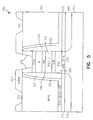
- FIG. 5is a cross-sectional view of a portion of a flash memory cell fabricated by using some of the steps illustrated in FIG. 2.
- FIG. 6is a cross-sectional view of a portion of the flash memory cell at a subsequent stage to that illustrated in FIG. 5, fabricated by using some of the steps illustrated in FIG. 3.
- FIG. 7is a cross-sectional view of a portion of the flash memory cell at a subsequent stage to that illustrated in FIG. 6, fabricated by using the remaining steps illustrated in FIG. 3.
- FIGS. 8 and 9illustrate top views of etched patterns in the first and second hard mask layers.
- FIG. 10is a perspective view of a memory cell array fabricated using the steps illustrated in FIGS. 1, 2, 3 , and 4 .
- FIG. 11is a block diagram of an exemplary computer system.
- FIG. 12is a block diagram of an exemplary memory system.
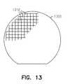
- FIG. 13is an elevation view of a substrate containing semiconductor dies.
- substrateused in the following description may include any semiconductor-based structure that has an exposed silicon surface. Structure must be understood to include silicon-on insulator (SOI), silicon-on sapphire (SOS), doped and undoped semiconductors, epitaxial layers of silicon supported by a base semiconductor foundation, and other semiconductor structures.
- SOIsilicon-on insulator
- SOSsilicon-on sapphire
- the semiconductorneed not be silicon-based.
- the semiconductorcould be silicon carbide, silicon-germanium, germanium, or gallium arsenide.
- previous process stepsmay be utilized to form regions, junctions, or layers in or on the base semiconductor or foundation.
- the present inventionprovides a technique for fabricating a memory cell array on a substrate to reduce cell size and to make the fabrication process more robust, less complex, and more cost effective.
- the fabrication techniqueincludes forming discrete and self-aligned contacts to each of the source and drain junctions in the memory cell array disposed on a semiconductor substrate.
- the techniquefarther includes forming self-aligned local area interconnects to form a common source region between each of the cells within each of the rows, in the array to reduce the possibility that the formed contacts will touch the gate structures of the memory cell array, and thereby significantly reducing the chances of shorting the gate structures.
- the formed contacts and interconnectsare plugged and filled with a conductive material to form the memory cell array.
- the fabrication technique of the present inventionuses self-aligned contact structures and local area interconnects to relax contact-to-gate spacing requirements to reduce the cell size and to further enhance the robustness of the fabrication process of the memory cell array.
- the techniqueallows forming discrete and similarly sized contacts to both the source and drain regions, which makes the SAC process more controllable and repeatable, thereby enhancing the robustness of the fabrication of the array.
- the techniquefurther forms a shunt layer for the source junctions and contact extensions for the drain contacts, and further allows for a self-aligned via to contact process.
- the advantage of using such local area interconnectsis that the source rail resistance is no longer dependant on the doping profile of the source junction. This allows doping of the source junction to be scaled back, leading to more aggressive scaling of the channel length.
- source rail resistancecan be greatly reduced, there is no longer a need to include a source contact for every 16 cells.
- the number of source contacts, per row within a blockcan now be scaled back to only two. There is one contact at the right edge of each block and one contact at the left edge of each block.
- the techniquerequires only one doped oxide etch for forming all of the SAC and non-SAC contacts, the shunt layer and the contact extensions.
- the techniquerequires only one metal stack deposition and one CMP to fill all of the SAC and non-SAC contacts, the shunt layer, and the contact extensions. This leads to a smaller flash cell/array due to a reduced contact-to-gate area (because of the use of SAC contact), and source junction scaling (reduced channel length due to the use of local area interconnect).
- this techniqueleads to a lower cost because the doped oxide etch and the single step metal deposition/CMP processes are combined into one single process step. This technique further results in improving the wafer/die yield due to forming substantially similarly sized contacts, which results in a more controlled and repeatable SAC process.
- Exemplary flow diagram 100includes blocks 110 - 130 that illustrate fabricating a memory cell array on a substrate.
- the arrayincludes memory cells arranged in rows and columns.
- Each of the memory cells in the arrayincludes a stacked gate, a source, and a drain. Further, each source and drain in the array includes corresponding source and drain junctions.
- the memory cell arraycan be a flash memory cell array, a memory circuit including an array of memory cells disposed on a substrate and/or a logic circuit including an array of memory cells.
- Block 110includes forming discrete and substantially similarly sized self-aligned source and drain contacts in a first layer disposed over the array to each of the source and drain junctions in the array.
- Block 120includes forming self-aligned local area slotted vias in a second layer disposed over the first layer. Each of the self-aligned local area slotted vias form local area interconnects that electrically shunt all of the source junction to the cells in each of the rows in the array. Further, block 120 includes forming discrete self-aligned drain extension over each of the formed self-aligned drain contacts to electrically connect the drains junctions to the drain extensions.
- Block 130includes simultaneously plugging and filling each of the formed self-aligned contacts, drain extensions, and slotted vias with a conductive material to form the memory cell array.
- the fabricated memory cell arrayincludes self-aligned drain contacts and slotted local area interconnects that electrically shunt all of the source junctions.
- FIG. 2is a flow diagram 200 of one exemplary method of forming discrete and similarly sized self-aligned source and drains contacts in the first layer of the memory cell array shown in FIG. 1.
- Exemplary flow diagram 200includes blocks 210 - 250 .
- Block 210includes depositing an undoped TEOS CVD oxide (tetraethylorthosilicate Si (OC 2 H 5 ) 4 ) layer over the memory cell array.
- the thickness of the undoped TEOS CVD oxide layercan be in the range of about 200-500 Angstroms.
- the memory cell arrayis formed on a substrate.
- the substratecan be formed from monocrystalline silicon material.
- Block 220includes depositing a first doped oxide layer such that the deposited first doped oxide layer is deposited over the deposited TEOS CVD oxide layer such that the first doped oxide layer fills unfilled portions around each of the source and the drain in the array and further the deposed first doped oxide layer is higher than the stacked gate.
- the first doped oxide layeris deposited using materials such as BPSG (borophosphosilicate glass), BSG (borosilicate glass), and/or PSG (phosphosilicate glass).
- the thickness of the first doped oxide layercan be in the range of about 5,000-18,000 Angstroms.
- Block 230includes planarizing to remove the excess deposited first doped oxide layer such that the first doped oxide layer is in the same plane as the top of the stacked gate.
- planarizingis done using processes such as a chemical-mechanical polishing process.
- planarizingincludes removing the excess first doped oxide layer such that the first doped oxide layer stops on the nitride cap layer.
- the top of the stacked gateincludes a desired nitride cap layer.
- Block 240includes depositing a first hard mask layer over the planarized first doped oxide layer and the top of the stacked gate.
- the first hard mask layercan be deposited using nitride.
- the thickness of the first hard mask layercan be in the range of about 200 to 1500 Angstroms.
- Block 250includes etching desired patterns in the first hard mask layer to define the shape and position of each of the self-aligned contacts for the source, drain, and gate stack regions. Etching of the first hard mask layer is performed such that it stops on the deposited first doped oxide layer to form the source and drain contacts. In some embodiments, etching desired patterns in the first hard mask layer is performed by first masking the first hard mask layer to provide exposed etching patterns on top of the first hard mask layer to receive the self-aligned contacts over the source and the drain junctions. Then etching the exposed etching patterns in the first hard mask layer to receive self-aligned contacts over source and drain junctions by stopping the etching on the deposited doped oxide layer.
- FIG. 3is a flow diagram 300 of one exemplary method of forming self-aligned local area slotted vias in a second layer disposed over the first layer to form local area interconnects.
- Each of the formed local area interconnectselectrically shunt all of the source junctions through the formed source contacts of the cells in each of the rows in the array.
- the methodincludes forming discrete self-aligned extensions over each of the formed self-aligned drain contacts to electrically connect the drain junctions through the drain contacts to the extensions.
- Exemplary flow diagram 300includes blocks 310 - 350 .
- Block 310includes depositing a second doped oxide layer over the deposited first hard mask layer and the etched patterns.
- the second doped oxide layeris deposited using materials such as BPSG (borophosphosilicate glass), BSG, and/or PSG.
- BPSGborophosphosilicate glass
- BSGborophosphosilicate glass
- PSGPSG
- the thickness of the second doped oxide layercan be in the range of about 2,000-6,000 Angstroms.
- Block 320includes depositing a second hard mask layer over the deposited second doped oxide layer.
- the first hard mask layercan be deposited using nitride.
- the thickness of the first hard mask layercan be in the range of about 200 to 1500 Angstroms.
- Block 330includes etching desired patterns in the second hard mask layer to define the shape and position of each of the self-aligned local area slotted vias that form local area interconnects to electrically shunt all of the source junctions through the source contacts in each row in the array.
- etching the desired patterns in the second hard mask layerincludes masking the second hard mask layer to expose the patterns for the slotted vias to receive long bar contacts that electrically shunt all of the source junctions and the discrete extensions over each of the formed discrete contacts and poly contacts.
- Block 340includes etching the exposed patterns in the underlying second doped oxide layer.
- exposed patternsare etched using an oxide etch that is selective to nitride to obtain desired patterns in the second doped oxide layer.
- Block 350includes further etching patterns defined by the patterns in the first hard mask layer in the first doped oxide layer to form the initial self-aligned contacts to the junctions. Etching the first and second doped oxide layers is performed under a self-aligned contact etch process using both the patterned hard masks and the nitride spacers along the cell's sidewalls, to guide, or self-align the etch process.
- the self-aligned local area interconnectsare formed using a dual damascene process.
- the first doped oxide layeris etched with an oxide etch that is selective to nitride to form the self-aligned contacts.
- FIG. 4is a flow diagram 400 of another exemplary method of forming the memory array by plugging and filling the formed contacts and slotted vias with a conductive material, as described with reference to FIGS. 2 and 3.
- Exemplary flow diagram 400includes blocks 410 - 480 .
- Block 410includes depositing a conductive material in the formed self-aligned contacts and slotted vias. Filling the discrete contacts and the slotted vias with a conductive material is accomplished in one single step, thereby eliminating the need to plug and fill the conductive material in two separate steps for the first and second layers of the array.
- the conductive material used in plugging and filling the formed contacts and viasinclude, for example, tungsten, aluminum, copper, titanium, tantalum, cobalt, molybdenum, tungsten silicide, titanium silicide, tantalum silicide, cobalt silicide, molybdenum silicide, and/or any combination of the above films.
- Block 420includes planarizing the deposited conductive material to the second hard mask layer by removing any excess conductive material deposited during the plugging and filling process described above. Planarizing the conductive material can be accomplished using techniques such as a chemical-mechanical polishing and/or a plug etch-back process.
- Block 430includes depositing a third doped oxide layer over the planarized conductive material and the deposited second hard mask layer.
- the third doped oxide layeris deposited using materials such as BPSG (borophosphosilicate glass), BSG, and/or PSG.
- BPSGborophosphosilicate glass
- BSGborophosphosilicate glass
- PSGPSG
- the thickness of the third doped oxide layercan be in the range of about 2,000-6,000 Angstroms.
- Block 440includes etching desired patterns in the third doped oxide layer such that the patterns opens up discrete vias to the underlying discrete extensions and contacts connecting to the drain junctions and shunt layer, as well as contacts to the gate stack.
- Block 450includes coating a thin layer of barrier metal over the opened drain vias in the third doped oxide layer.
- barrier metalcan be titanium followed by titanium nitride (Ti/TiN) and for copper plug the barrier metal can tantalum nitride (TaN).
- Block 460includes filling the coated drain vias with a conductive material to electrically connect with the exposed discrete extensions in the second doped oxide layer.
- the conductive material used in filling the drain viascan include tungsten, aluminum, copper, titanium, tantalum, cobalt, molybdenum, tungsten silicide, titanium silicide, tantalum silicide, cobalt silicide, and/or molybdenum silicide.
- Block 470includes planarizing the plugged drain vias to remove any excess deposited conductive material to be in plane with outer exposed third doped oxide layer.
- Block 480includes depositing a first level metallization on the outer exposed third doped oxide layer to electrically connect all established discrete drain contacts in the array.
- FIGS. 5 - 9show the memory cell structure 500 in the processing state shown in FIGS. 1, 2, 3 , and 4 .
- the memory cell structure 500 shown in FIG. 5includes a substrate 510 having a gate stack 520 of a memory cell formed according to well-known semiconductor processing techniques. For simiplicity and a better understanding of the memory cell structure, only one gate stack is shown in FIG. 5, it can be envisioned that the substrate includes an array of memory cells including similar gate stacks.
- FIG. 5illustrates the formed discrete and substantially similarly sized self-aligned contacts in the first hard mask layer 590 over the memory cell structure 500 .
- the gate stack 520 shown in FIG. 5,includes an oxide layer 530 , an electrically insulated conductive layer 540 , such as poly-silicon, and a high coupling dielectric cell stack including oxide-nitride-oxide, a second poly-silicon layer 542 , which is typically directly layered to a metal shunt layer, nitride spacers 525 , and a nitride cap 550 .
- the shunt metal layercould be formed using either a pure metal such as tungsten/tungsten nitride or a refractory metal silicide layer 545 .
- a refractory metal silicide layermay comprise any refractory metal, including but not limited to, titanium, tungsten, cobalt, tantalum, and molybdenum.
- the refractory metal silicide layeris substantially composed of tungsten silicide (WSi x ).
- a TEOS (tetraethylorthosilicate) layeris formed over nitride spacers 525 .
- An insulating oxide layer 560covers the substrate 510 , which contains the gate stack 520 and active regions. Also shown in FIG. 5 are source and drain junctions 570 and 580 , respectively of the memory cell structure 500 . In some embodiments, a thermal oxide layer 575 is formed over the drain and source junctions 570 and 580 , respectively.
- BPSGborophosphosilicate glass
- BSGborosilicate glass
- PSGphosphosilicate glass
- the processing state shown in FIG. 5includes a first hard mask layer 590 deposited as described in more detail with reference to FIG. 2. Also, shown are the etched desired patterns 595 in the first hard mask layer 590 defining the shape and position of each of the self-aligned contacts for the source, drain, and gate stack regions by stopping the etching on the deposited first doped oxide layer. The process of etching the desired patterns 595 for the self-aligned contacts has been described in more detail with reference to FIG. 2.
- FIG. 6illustrates memory cell structure 600 including the second doped oxide layer 610 deposited over the first hard mask layer 590 .
- FIG. 6further shows second hard mask layer 620 deposited over the second doped oxide layer 610 . The process of depositing the second doped oxide layer 610 and the second hard mask layer 620 is described in more detail with reference to FIG. 3.
- FIG. 7illustrates memory cell structure 700 including a formed self-aligned local area slotted via in the second doped oxide layer 610 and the second hard mask layer 620 that shunts all source junctions in the memory cell structure 700 . Also, shown in FIG. 7 is formed discrete self-aligned drain extension 720 in the second doped oxide layer 610 and the second hard mask layer 620 . Also, shown are formed discrete self-aligned drain, source, and gate contacts 730 , 740 , and 750 in the first doped oxide and hard mask layers 560 and 590 , respectively.
- slotted via 710 , drain extension 720 , and the source and drain contacts 730 and 740are described in more detail with reference to FIGS. 2 and 3. It can be seen from FIG. 7 that the slotted via 710 , drain extension 720 , and source and drain contacts 730 and 740 can be plugged and filled with a conductive material in one single step.
- the thickness of the doped oxide layers 560 and 610 shown in FIGS. 5 and 6are approximately in the range of about 5000 to 18000 Angstroms.
- the thickness of the hard mask layers 590 and 620is in the range of about 200 to 1500 Angstroms.
- the hard mask layers 590 and 620 shown in FIGS. 5 and 6can be made from materials such as nitride.
- the contacts and the interconnects 710 , 720 , 730 , and 740can be plugged and filled with conductive materials, such as tungsten, aluminum, copper, titanium, tantalum, cobalt, molybdenum, tungsten silicide, titanium silicide, tantalum silicide, cobalt silicide, and/or molybdenum silicide.
- conductive materialssuch as tungsten, aluminum, copper, titanium, tantalum, cobalt, molybdenum, tungsten silicide, titanium silicide, tantalum silicide, cobalt silicide, and/or molybdenum silicide.
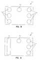
- FIG. 8illustrates a top view 800 showing the formed discrete and substantially similarly sized self-aligned source, drain, and gate contacts 730 , 740 , and 750 in the first layer including the first doped oxide and hard mask layers 560 and 590 .
- the process of forming desired etch patterns for the discrete source and drain contacts 730 and 740is described in more detail with reference to FIG. 2.
- the top view 800only shows a few source and drain contacts 730 and 740 .
- the top view 800shows the gate stack 750 being in close proximity with the source and drain contacts 730 and 740 .
- a memory cell structurehas many more source and drain contacts, and the gate stack is not located this close to the source and drain contacts.
- FIG. 9illustrates a top view 900 showing slotted via 710 , drain extension 720 , and gate via 760 in the second doped oxide and hard mask layers 610 and 620 , respectively over formed source, drain, and gate contacts 730 , 740 , and 760 .
- the process of forming desired patterns for slotted via 710 and drain extension 720is described in more detail with reference to FIG. 3.
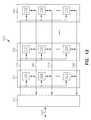
- FIG. 10shows formed memory cell array 1000 using the steps illustrated in FIGS. 2 - 4 .
- the memory cell array shown in FIG. 10includes the various stages illustrated in FIGS. 5 - 7 .
- memory cell array 1000further includes a third doped oxide layer 1010 , discrete drain connections 1020 to establish connection with the exposed discrete drain extensions 720 , and a first level metallization 1030 on the outer exposed third doped oxide layer 1010 to electrically connect all of the established discrete drain contacts in array 1000 .
- the formed memory cell arraycan be a flash memory cell array, a memory circuit on a semiconductor substrate, and/or a logic circuit including an array of memory cells.
- the fabrication technique used in forming memory cell structure 1000 using the various stages illustrated in FIGS. 5 - 9includes forming discrete and self-aligned contacts to each of the drains in the memory cell array disposed on a semiconductor substrate 510 .
- the techniquefurther includes forming self-aligned local area interconnects 710 to form a common source region between each of the cells, within each of the rows in the array to reduce the possibility that the formed contacts will touch the gate structures of memory cell array 1000 . This significantly reduces the chances of shorting the gate structures.
- the formed contacts 720 , 730 , and 740 and interconnects 710are plugged and filled with a conductive material to form the memory cell array 1000 shown in FIG. 10.
- the fabrication technique of the present inventionuses self-aligned contact structures 720 , 730 , and 740 and local area interconnects 710 to relax contact-to-gate spacing requirements to reduce the cell size and to further enhance the robustness of the fabrication process of memory cell array 1000 .
- the techniqueallows discrete and similarly sized contacts 730 and 740 (shown in FIG. 8) to form both the source and drain regions in a single step. This makes the SAC process more controllable and repeatable, thereby enhancing the robustness of the fabrication process.
- the techniquefurther forms a shunt layer for the source junctions and contact extensions for the drain contacts, and further allows for a self-aligned via-to-contact process.
- the advantage of using such local area interconnects 710is that the source rail resistance is no longer dependant on the doping profile of the source junction. This allows doping of the source junction to be scaled back, leading to more aggressive scaling of the channel length.
- the source rail resistanceis greatly reduced, there is no longer a need to have a source contact for every 16 cells.
- the number of source contacts, per row within a blockcan now be scaled back to only two: one contact at the right edge of each block and the other contact at the left edge of each block.
- the techniquerequires only one doped oxide etch to form all SAC contacts 730 and 740 and non-SAC contacts 750 , shunt layer and contact extensions 710 , 720 , and 760 .
- the techniquerequires only one metal stack deposition and one CMP to fill all SAC and non-SAC contacts, the shunt layer, and the contact extensions as shown in FIG. 7. Due to a reduced contact-to-gate area (because of the use of SAC contact) and source junction scaling (reduced channel length due to the use of local area interconnect), a smaller flash cell/array is produced. Further, by combining the doped oxide etch and the single step metal deposition/CMP processes, costs are significantly lowered. This technique further results in improved wafer/die yield due to the formation of substantially similarly sized contacts, which results in a more controlled and repeatable SAC process.
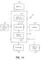
- FIG. 11is a block diagram of a system according to one embodiment of the present invention.
- Computer system 1100contains a processor 1110 and a memory system 1102 housed in a computer unit 1105 .
- Computer system 1100is but one example of an electronic system containing another electronic system, e.g., memory system 1102 , as a subcomponent.
- the memory system 1102includes a memory device that includes a memory cell array as discussed in various embodiments of the present invention.
- Computer system 1100optionally contains user interface components. These user interface components include a keyboard 1120 , a pointing device 1130 , a monitor 1140 , a printer 1150 , and a bulk storage device 1160 .
- processor 1110 and memory system 1102 of computer system 1100can be incorporated on a single integrated circuit. Such single-package processing units reduce the communication time between the processor and the memory circuit. Any of these components of the system may contain a memory device that includes the multiple-mode output driver of the present invention. This is particularly true of a graphics subsystem 1170 of FIG. 11 utilizing SGRAM that includes the multiple-mode output driver as discussed in various embodiments of the present invention.
- FIG. 12is a block diagram of a system according to one embodiment of the present invention.
- Memory system 1200contains one or more memory modules 1202 and a memory controller 1212 .
- Each memory module 1202includes at least one memory device 1210 .
- Memory controller 1212provides and controls a bidirectional interface between memory system 1200 and an external system bus 1220 .
- Memory system 1200accepts a command signal from the external bus 1220 and relays it to the one or more memory modules 1202 on a command link 1230 .
- Memory system 1200provides for data input and data output between the one or more memory modules 1202 and external system bus 1220 on data links 1240 .
- At least one of the memory devices 1210includes the memory cell array as discussed in various embodiments of the present invention.
- a semiconductor die 1310is produced from a silicon wafer 1300 .
- a dieis an individual pattern, typically rectangular, on a substrate that contains circuitry to perform a specific function.
- a semiconductor waferwill typically contain a repeated pattern of such dies containing the same functionality.
- Die 1310may contain circuitry for the memory device, as discussed above. Die 1310 may further contain additional circuitry to extend to such complex devices as a monolithic processor with multiple functionality.
- Die 1310is typically packaged in a protective casing (not shown) with leads extending therefrom (not shown) providing access to the circuitry of the die for unilateral or bilateral communication and control.
Landscapes
- Engineering & Computer Science (AREA)
- Physics & Mathematics (AREA)
- Condensed Matter Physics & Semiconductors (AREA)
- General Physics & Mathematics (AREA)
- Manufacturing & Machinery (AREA)
- Computer Hardware Design (AREA)
- Microelectronics & Electronic Packaging (AREA)
- Power Engineering (AREA)
- Semiconductor Memories (AREA)
- Internal Circuitry In Semiconductor Integrated Circuit Devices (AREA)
Abstract
Description
- The present invention relates to fabrication of integrated circuits and, in particular, to fabrication of memory array logic devices requiring both self-aligned contact structures and local area interconnects.[0001]
- Contacts are required in an integrated circuit device to provide electrical connections between layers or levels of the integrated circuit device. Semiconductor devices typically include a multitude of transistors, which are coupled together in particular configurations through the use of contacts.[0002]
- A conventional flash memory module includes multiple memory cells. A memory cell includes a stacked gate, a drain, and a source. A drain contact electrically connects the drain of each memory cell to a conductive layer (a bit line) above the stacked gate. The conductive layer can be a aluminum layer. For a NOR type of memory array, a common/single source contact connects the source junctions of a number of memory cells. This common source contact is generally referred to as a “source rail.”[0003]
- There is increasing pressure in the current semiconductor industry to achieve higher device density within a given die area. This is particularly true in memory circuit fabrication, such as a flash memory manufacture. In recent years, the number and density of these memory cells on the flash memory module has dramatically increased so that the number of memory cells on a single chip is expected to soon reach 1 Gigabit. Increases in semiconductor packing density and downsizing of individual devices has resulted in increases in circuit density. Many aspects of the semiconductor fabrication process are affected by the demand for density increases in device packing. Feature alignment from one semiconductor level to the next is of critical importance, particularly relating to the alignment of contact holes with the underlying structures with which they are to connect, such as active areas. Device miniaturization complicates the process of forming interconnect structures because in order to maintain sufficient electrical communication, the interconnect structure must be formed in exact alignment with an underlying active region. At the same time, the area of the interconnect structure interfacing with the active area must be maximized. Thus, as device sizes shrink there is less room for misalignment errors of the interconnect structure.[0004]
- Device size reductions are due in part to advances in photolithography and directional (anisotropic) plasma etching. Because horizontal device feature sizes are approaching deep submicrometer dimensions, self-alignment techniques are employed to relax the alignment requirements and improve critical dimension (CD) control. One such self-alignment technique is called self-aligned contact (SAC) etching. In SAC etching, a pair of adjacent gate stacks are utilized to align an etched opening in an insulating layer.[0005]
- Currently there are possible options for a flash memory module to utilize the self-aligned contact process. The first option is to limit the SAC process to the current location for making contact to both the source and the drain junctions. In this case, a scaled process would still be limited by high source rail resistance and/or excess source junction overlap with the gate stack.[0006]
- The second option would be to merge a local area interconnect and the SAC process together. The problem with this option being is that you have to etch both a long slotted contact over the source junctions and discrete round contacts over the drain junctions. Etching of the SAC contact is generally very shape sensitive and etching of such multiple shapes during the self-aligned contact process can result in significant etch problems and self-aligned contact problems. In addition, the long slotted contact would be passing over both active junction regions and field isolation regions. The etch would ideally have to be selective to field isolation. This is somewhat difficult, because the material used for the field isolation and the undoped glass, under the borophosphosilicate glass (BPSG) are very similar.[0007]
- The third possible option is to limit the SAC etch contact to one size only, all having a discrete round pattern. The problem with this approach is that the source contacts are not linked together and an additional shunting layer must be patterned (resulting in a second lithography level), etched (resulting in a second etch step), and formed for the source junctions (resulting in a second metal deposition and chemical-mechanical polishing (CMP)).[0008]
- As device sizes are reduced, smaller dimensions are required to achieve higher packing densities. The spacing between the contacts and the gate can significantly contribute to the overall size of the flash memory cell. Simply reducing the space between the contacts and the gate makes the fabrication process less robust, more complex for the lithography process, and less cost effective due to yield loss resulting from alignment errors.[0009]
- Thus, there is a need in the art to relax contact-to-gate spacing, making the SAC contact a requirement. In addition, there is a need for a flash memory with a smaller cell channel length, which will require the use of a local interconnect. Further still, there is an overall need to reduce the cost of the process flow, which in combination with all of the above, requires the memory cell fabrication process to be more robust, less complex, and more cost effective.[0010]
- The present invention provides an advanced metallization technique for fabricating a flash memory cell array on a substrate to reduce cell size and make the fabrication process more robust, less complex, and more cost effective.[0011]
- The array is fabricated by forming discrete and substantially similarly sized self-aligned contacts in a first layer disposed over the array to form contacts to each of the source and drain junctions in the array. Further, self-aligned local area slotted vias in a second layer disposed over the first layer form local area interconnects that electrically shunt all of the source contacts/junctions. In addition, discrete self-aligned drain extensions are formed over each of the formed drain contacts. Plugging and filling the formed self-aligned contacts, drain extensions, and the slotted local area vias with a conductive material is performed in a single step to form the array including the discrete self-aligned drain contacts and local area interconnects shunting the source junctions in each of the rows in the array.[0012]
- Additional advantages and features of the present invention will be more apparent from the detailed description and accompanying drawings, which illustrate preferred embodiments of the invention.[0013]
- FIG. 1 is a flow diagram of fabricating a memory array according to the present invention.[0014]
- FIG. 2 is a flow diagram of one exemplary method of forming self-aligned contacts of a flash memory array fabricated according to the present invention.[0015]
- FIG. 3 is a flow diagram of one exemplary method of forming self-aligned local area slotted vias according to the present invention.[0016]
- FIG. 4 is a flow diagram of another exemplary method of forming the memory array by using the formed contacts and vias as illustrated in FIGS. 2 and 3 according to the present invention.[0017]
- FIG. 5 is a cross-sectional view of a portion of a flash memory cell fabricated by using some of the steps illustrated in FIG. 2.[0018]
- FIG. 6 is a cross-sectional view of a portion of the flash memory cell at a subsequent stage to that illustrated in FIG. 5, fabricated by using some of the steps illustrated in FIG. 3.[0019]
- FIG. 7 is a cross-sectional view of a portion of the flash memory cell at a subsequent stage to that illustrated in FIG. 6, fabricated by using the remaining steps illustrated in FIG. 3.[0020]
- FIGS. 8 and 9 illustrate top views of etched patterns in the first and second hard mask layers.[0021]
- FIG. 10 is a perspective view of a memory cell array fabricated using the steps illustrated in FIGS. 1, 2,[0022]3, and4.
- FIG. 11 is a block diagram of an exemplary computer system.[0023]
- FIG. 12 is a block diagram of an exemplary memory system.[0024]
- FIG. 13 is an elevation view of a substrate containing semiconductor dies.[0025]
- In the following detailed description, reference is made to various specific embodiments in which the invention may be practiced. These embodiments are described with sufficient detail to enable those skilled in the art to practice the invention, and it is to be understood that other embodiments may be employed, and that structural, logical, electrical, and process changes may be made without departing from the teachings of the invention.[0026]
- In the foregoing description of the preferred embodiments, various features of the invention are grouped together in a single embodiment for the purpose of streamlining the disclosure. This method of disclosure is not to be interpreted as reflecting an intention that the claimed invention requires more features than are expressly recited in each claim. Rather, as the following claims reflect, inventive aspects lie in less than all features of a single disclosed embodiment. Thus, the following claims are hereby incorporated into the description of the preferred embodiments, with each claim standing on its own as a separate preferred embodiment of the invention.[0027]
- The term “substrate” used in the following description may include any semiconductor-based structure that has an exposed silicon surface. Structure must be understood to include silicon-on insulator (SOI), silicon-on sapphire (SOS), doped and undoped semiconductors, epitaxial layers of silicon supported by a base semiconductor foundation, and other semiconductor structures. The semiconductor need not be silicon-based. The semiconductor could be silicon carbide, silicon-germanium, germanium, or gallium arsenide. When reference is made to a wafer or substrate in the following description, previous process steps may be utilized to form regions, junctions, or layers in or on the base semiconductor or foundation.[0028]
- In the discussion which follows, the invention is described with reference to a self-aligned contact etch as used in the fabrication of memory devices. However, it should be understood that the invention pertains to any applications which require selectivity to an undoped oxide isolation region during the etch of doped silicon oxide dielectric layers.[0029]
- The present invention provides a technique for fabricating a memory cell array on a substrate to reduce cell size and to make the fabrication process more robust, less complex, and more cost effective.[0030]
- The fabrication technique includes forming discrete and self-aligned contacts to each of the source and drain junctions in the memory cell array disposed on a semiconductor substrate. The technique farther includes forming self-aligned local area interconnects to form a common source region between each of the cells within each of the rows, in the array to reduce the possibility that the formed contacts will touch the gate structures of the memory cell array, and thereby significantly reducing the chances of shorting the gate structures. Finally, the formed contacts and interconnects are plugged and filled with a conductive material to form the memory cell array.[0031]
- The fabrication technique of the present invention uses self-aligned contact structures and local area interconnects to relax contact-to-gate spacing requirements to reduce the cell size and to further enhance the robustness of the fabrication process of the memory cell array. The technique allows forming discrete and similarly sized contacts to both the source and drain regions, which makes the SAC process more controllable and repeatable, thereby enhancing the robustness of the fabrication of the array.[0032]
- The technique further forms a shunt layer for the source junctions and contact extensions for the drain contacts, and further allows for a self-aligned via to contact process. The advantage of using such local area interconnects, is that the source rail resistance is no longer dependant on the doping profile of the source junction. This allows doping of the source junction to be scaled back, leading to more aggressive scaling of the channel length. In addition, since source rail resistance can be greatly reduced, there is no longer a need to include a source contact for every 16 cells. The number of source contacts, per row within a block, can now be scaled back to only two. There is one contact at the right edge of each block and one contact at the left edge of each block.[0033]
- Also, the technique requires only one doped oxide etch for forming all of the SAC and non-SAC contacts, the shunt layer and the contact extensions. In addition, the technique requires only one metal stack deposition and one CMP to fill all of the SAC and non-SAC contacts, the shunt layer, and the contact extensions. This leads to a smaller flash cell/array due to a reduced contact-to-gate area (because of the use of SAC contact), and source junction scaling (reduced channel length due to the use of local area interconnect). Further, this technique leads to a lower cost because the doped oxide etch and the single step metal deposition/CMP processes are combined into one single process step. This technique further results in improving the wafer/die yield due to forming substantially similarly sized contacts, which results in a more controlled and repeatable SAC process.[0034]
- Referring now to FIG. 1, a representative flow diagram[0035]100 according to the present invention. Exemplary flow diagram100 includes blocks110-130 that illustrate fabricating a memory cell array on a substrate. The array includes memory cells arranged in rows and columns. Each of the memory cells in the array includes a stacked gate, a source, and a drain. Further, each source and drain in the array includes corresponding source and drain junctions. In some embodiments, the memory cell array can be a flash memory cell array, a memory circuit including an array of memory cells disposed on a substrate and/or a logic circuit including an array of memory cells.
- [0036]
Block 110 includes forming discrete and substantially similarly sized self-aligned source and drain contacts in a first layer disposed over the array to each of the source and drain junctions in the array. - [0037]
Block 120 includes forming self-aligned local area slotted vias in a second layer disposed over the first layer. Each of the self-aligned local area slotted vias form local area interconnects that electrically shunt all of the source junction to the cells in each of the rows in the array. Further, block120 includes forming discrete self-aligned drain extension over each of the formed self-aligned drain contacts to electrically connect the drains junctions to the drain extensions. - [0038]
Block 130 includes simultaneously plugging and filling each of the formed self-aligned contacts, drain extensions, and slotted vias with a conductive material to form the memory cell array. The fabricated memory cell array includes self-aligned drain contacts and slotted local area interconnects that electrically shunt all of the source junctions. - FIG. 2 is a flow diagram[0039]200 of one exemplary method of forming discrete and similarly sized self-aligned source and drains contacts in the first layer of the memory cell array shown in FIG. 1. Exemplary flow diagram200 includes blocks210-250.
Block 210 includes depositing an undoped TEOS CVD oxide (tetraethylorthosilicate Si (OC2H5)4) layer over the memory cell array. The thickness of the undoped TEOS CVD oxide layer can be in the range of about 200-500 Angstroms. The memory cell array is formed on a substrate. The substrate can be formed from monocrystalline silicon material. - [0040]
Block 220 includes depositing a first doped oxide layer such that the deposited first doped oxide layer is deposited over the deposited TEOS CVD oxide layer such that the first doped oxide layer fills unfilled portions around each of the source and the drain in the array and further the deposed first doped oxide layer is higher than the stacked gate. In some embodiments, the first doped oxide layer is deposited using materials such as BPSG (borophosphosilicate glass), BSG (borosilicate glass), and/or PSG (phosphosilicate glass). The thickness of the first doped oxide layer can be in the range of about 5,000-18,000 Angstroms. - [0041]
Block 230 includes planarizing to remove the excess deposited first doped oxide layer such that the first doped oxide layer is in the same plane as the top of the stacked gate. In some embodiments, planarizing is done using processes such as a chemical-mechanical polishing process. In some embodiments, planarizing includes removing the excess first doped oxide layer such that the first doped oxide layer stops on the nitride cap layer. Generally, the top of the stacked gate includes a desired nitride cap layer. - [0042]
Block 240 includes depositing a first hard mask layer over the planarized first doped oxide layer and the top of the stacked gate. In some embodiments, the first hard mask layer can be deposited using nitride. The thickness of the first hard mask layer can be in the range of about 200 to 1500 Angstroms. - [0043]
Block 250 includes etching desired patterns in the first hard mask layer to define the shape and position of each of the self-aligned contacts for the source, drain, and gate stack regions. Etching of the first hard mask layer is performed such that it stops on the deposited first doped oxide layer to form the source and drain contacts. In some embodiments, etching desired patterns in the first hard mask layer is performed by first masking the first hard mask layer to provide exposed etching patterns on top of the first hard mask layer to receive the self-aligned contacts over the source and the drain junctions. Then etching the exposed etching patterns in the first hard mask layer to receive self-aligned contacts over source and drain junctions by stopping the etching on the deposited doped oxide layer. - FIG. 3 is a flow diagram[0044]300 of one exemplary method of forming self-aligned local area slotted vias in a second layer disposed over the first layer to form local area interconnects. Each of the formed local area interconnects electrically shunt all of the source junctions through the formed source contacts of the cells in each of the rows in the array. Further the method includes forming discrete self-aligned extensions over each of the formed self-aligned drain contacts to electrically connect the drain junctions through the drain contacts to the extensions. Exemplary flow diagram300 includes blocks310-350.
- [0045]
Block 310 includes depositing a second doped oxide layer over the deposited first hard mask layer and the etched patterns. In some embodiments, the second doped oxide layer is deposited using materials such as BPSG (borophosphosilicate glass), BSG, and/or PSG. The thickness of the second doped oxide layer can be in the range of about 2,000-6,000 Angstroms. - [0046]
Block 320 includes depositing a second hard mask layer over the deposited second doped oxide layer. In some embodiments, the first hard mask layer can be deposited using nitride. The thickness of the first hard mask layer can be in the range of about 200 to 1500 Angstroms. - [0047]
Block 330 includes etching desired patterns in the second hard mask layer to define the shape and position of each of the self-aligned local area slotted vias that form local area interconnects to electrically shunt all of the source junctions through the source contacts in each row in the array. In some embodiments, etching the desired patterns in the second hard mask layer includes masking the second hard mask layer to expose the patterns for the slotted vias to receive long bar contacts that electrically shunt all of the source junctions and the discrete extensions over each of the formed discrete contacts and poly contacts.Block 340 includes etching the exposed patterns in the underlying second doped oxide layer. In some embodiments, exposed patterns are etched using an oxide etch that is selective to nitride to obtain desired patterns in the second doped oxide layer.Block 350 includes further etching patterns defined by the patterns in the first hard mask layer in the first doped oxide layer to form the initial self-aligned contacts to the junctions. Etching the first and second doped oxide layers is performed under a self-aligned contact etch process using both the patterned hard masks and the nitride spacers along the cell's sidewalls, to guide, or self-align the etch process. In some embodiments, the self-aligned local area interconnects are formed using a dual damascene process. In some embodiments, the first doped oxide layer is etched with an oxide etch that is selective to nitride to form the self-aligned contacts. - FIG. 4 is a flow diagram[0048]400 of another exemplary method of forming the memory array by plugging and filling the formed contacts and slotted vias with a conductive material, as described with reference to FIGS. 2 and 3. Exemplary flow diagram400 includes blocks410-480.
Block 410 includes depositing a conductive material in the formed self-aligned contacts and slotted vias. Filling the discrete contacts and the slotted vias with a conductive material is accomplished in one single step, thereby eliminating the need to plug and fill the conductive material in two separate steps for the first and second layers of the array. The conductive material used in plugging and filling the formed contacts and vias, include, for example, tungsten, aluminum, copper, titanium, tantalum, cobalt, molybdenum, tungsten silicide, titanium silicide, tantalum silicide, cobalt silicide, molybdenum silicide, and/or any combination of the above films. - [0049]
Block 420 includes planarizing the deposited conductive material to the second hard mask layer by removing any excess conductive material deposited during the plugging and filling process described above. Planarizing the conductive material can be accomplished using techniques such as a chemical-mechanical polishing and/or a plug etch-back process. - [0050]
Block 430 includes depositing a third doped oxide layer over the planarized conductive material and the deposited second hard mask layer. In some embodiments, the third doped oxide layer is deposited using materials such as BPSG (borophosphosilicate glass), BSG, and/or PSG. The thickness of the third doped oxide layer can be in the range of about 2,000-6,000 Angstroms. - [0051]
Block 440 includes etching desired patterns in the third doped oxide layer such that the patterns opens up discrete vias to the underlying discrete extensions and contacts connecting to the drain junctions and shunt layer, as well as contacts to the gate stack.Block 450 includes coating a thin layer of barrier metal over the opened drain vias in the third doped oxide layer. For example, for tungsten plug or aluminum plug, barrier metal can be titanium followed by titanium nitride (Ti/TiN) and for copper plug the barrier metal can tantalum nitride (TaN). - [0052]
Block 460 includes filling the coated drain vias with a conductive material to electrically connect with the exposed discrete extensions in the second doped oxide layer. The conductive material used in filling the drain vias can include tungsten, aluminum, copper, titanium, tantalum, cobalt, molybdenum, tungsten silicide, titanium silicide, tantalum silicide, cobalt silicide, and/or molybdenum silicide. - [0053]
Block 470 includes planarizing the plugged drain vias to remove any excess deposited conductive material to be in plane with outer exposed third doped oxide layer.Block 480 includes depositing a first level metallization on the outer exposed third doped oxide layer to electrically connect all established discrete drain contacts in the array. - FIGS.[0054]5-9 show the
memory cell structure 500 in the processing state shown in FIGS. 1, 2,3, and4. Thememory cell structure 500 shown in FIG. 5 includes asubstrate 510 having agate stack 520 of a memory cell formed according to well-known semiconductor processing techniques. For simiplicity and a better understanding of the memory cell structure, only one gate stack is shown in FIG. 5, it can be envisioned that the substrate includes an array of memory cells including similar gate stacks. - FIG. 5 illustrates the formed discrete and substantially similarly sized self-aligned contacts in the first[0055]
hard mask layer 590 over thememory cell structure 500. Thegate stack 520 shown in FIG. 5, includes anoxide layer 530, an electrically insulatedconductive layer 540, such as poly-silicon, and a high coupling dielectric cell stack including oxide-nitride-oxide, a second poly-silicon layer 542, which is typically directly layered to a metal shunt layer,nitride spacers 525, and anitride cap 550. The shunt metal layer could be formed using either a pure metal such as tungsten/tungsten nitride or a refractorymetal silicide layer 545. A refractory metal silicide layer may comprise any refractory metal, including but not limited to, titanium, tungsten, cobalt, tantalum, and molybdenum. Preferably, the refractory metal silicide layer is substantially composed of tungsten silicide (WSix). A TEOS (tetraethylorthosilicate) layer is formed overnitride spacers 525. - An insulating[0056]
oxide layer 560, for example a borophosphosilicate glass (BPSG), borosilicate glass (BSG), and/or phosphosilicate glass (PSG) layer, covers thesubstrate 510, which contains thegate stack 520 and active regions. Also shown in FIG. 5 are source and drainjunctions memory cell structure 500. In some embodiments, athermal oxide layer 575 is formed over the drain andsource junctions - The processing state shown in FIG. 5 includes a first[0057]
hard mask layer 590 deposited as described in more detail with reference to FIG. 2. Also, shown are the etched desiredpatterns 595 in the firsthard mask layer 590 defining the shape and position of each of the self-aligned contacts for the source, drain, and gate stack regions by stopping the etching on the deposited first doped oxide layer. The process of etching the desiredpatterns 595 for the self-aligned contacts has been described in more detail with reference to FIG. 2. - FIG. 6 illustrates[0058]
memory cell structure 600 including the seconddoped oxide layer 610 deposited over the firsthard mask layer 590. FIG. 6 further shows secondhard mask layer 620 deposited over the seconddoped oxide layer 610. The process of depositing the seconddoped oxide layer 610 and the secondhard mask layer 620 is described in more detail with reference to FIG. 3. - FIG. 7 illustrates[0059]
memory cell structure 700 including a formed self-aligned local area slotted via in the seconddoped oxide layer 610 and the secondhard mask layer 620 that shunts all source junctions in thememory cell structure 700. Also, shown in FIG. 7 is formed discrete self-aligneddrain extension 720 in the seconddoped oxide layer 610 and the secondhard mask layer 620. Also, shown are formed discrete self-aligned drain, source, andgate contacts drain extension 720, and the source anddrain contacts drain extension 720, and source anddrain contacts - The thickness of the doped[0060]
oxide layers interconnects - FIG. 8 illustrates a[0061]
top view 800 showing the formed discrete and substantially similarly sized self-aligned source, drain, andgate contacts drain contacts top view 800 only shows a few source anddrain contacts top view 800 shows thegate stack 750 being in close proximity with the source anddrain contacts - FIG. 9 illustrates a[0062]
top view 900 showing slotted via710,drain extension 720, and gate via760 in the second doped oxide and hard mask layers610 and620, respectively over formed source, drain, andgate contacts drain extension 720 is described in more detail with reference to FIG. 3. - FIG. 10 shows formed[0063]
memory cell array 1000 using the steps illustrated in FIGS.2-4. Also, the memory cell array shown in FIG. 10 includes the various stages illustrated in FIGS.5-7. In addition to what is shown in FIGS.5-7,memory cell array 1000 further includes a thirddoped oxide layer 1010,discrete drain connections 1020 to establish connection with the exposeddiscrete drain extensions 720, and afirst level metallization 1030 on the outer exposed thirddoped oxide layer 1010 to electrically connect all of the established discrete drain contacts inarray 1000. The formed memory cell array can be a flash memory cell array, a memory circuit on a semiconductor substrate, and/or a logic circuit including an array of memory cells. - The fabrication technique used in forming[0064]
memory cell structure 1000 using the various stages illustrated in FIGS.5-9, includes forming discrete and self-aligned contacts to each of the drains in the memory cell array disposed on asemiconductor substrate 510. The technique further includes forming self-aligned local area interconnects710 to form a common source region between each of the cells, within each of the rows in the array to reduce the possibility that the formed contacts will touch the gate structures ofmemory cell array 1000. This significantly reduces the chances of shorting the gate structures. Finally, the formedcontacts interconnects 710 are plugged and filled with a conductive material to form thememory cell array 1000 shown in FIG. 10. - The fabrication technique of the present invention uses self-aligned[0065]
contact structures memory cell array 1000. The technique allows discrete and similarlysized contacts 730 and740 (shown in FIG. 8) to form both the source and drain regions in a single step. This makes the SAC process more controllable and repeatable, thereby enhancing the robustness of the fabrication process. - The technique further forms a shunt layer for the source junctions and contact extensions for the drain contacts, and further allows for a self-aligned via-to-contact process. The advantage of using such local area interconnects[0066]710 is that the source rail resistance is no longer dependant on the doping profile of the source junction. This allows doping of the source junction to be scaled back, leading to more aggressive scaling of the channel length. In addition, since the source rail resistance is greatly reduced, there is no longer a need to have a source contact for every16 cells. The number of source contacts, per row within a block, can now be scaled back to only two: one contact at the right edge of each block and the other contact at the left edge of each block.
- In addition, the technique requires only one doped oxide etch to form all[0067]
SAC contacts non-SAC contacts 750, shunt layer andcontact extensions - FIG. 11 is a block diagram of a system according to one embodiment of the present invention.[0068]
Computer system 1100 contains aprocessor 1110 and amemory system 1102 housed in acomputer unit 1105.Computer system 1100 is but one example of an electronic system containing another electronic system, e.g.,memory system 1102, as a subcomponent. Thememory system 1102 includes a memory device that includes a memory cell array as discussed in various embodiments of the present invention.Computer system 1100 optionally contains user interface components. These user interface components include akeyboard 1120, apointing device 1130, amonitor 1140, aprinter 1150, and abulk storage device 1160. It will be appreciated that other components are often associated withcomputer system 1100 such as modems, device driver cards, additional storage devices, etc. It will further be appreciated that theprocessor 1110 andmemory system 1102 ofcomputer system 1100 can be incorporated on a single integrated circuit. Such single-package processing units reduce the communication time between the processor and the memory circuit. Any of these components of the system may contain a memory device that includes the multiple-mode output driver of the present invention. This is particularly true of agraphics subsystem 1170 of FIG. 11 utilizing SGRAM that includes the multiple-mode output driver as discussed in various embodiments of the present invention. - FIG. 12 is a block diagram of a system according to one embodiment of the present invention.[0069]
Memory system 1200 contains one ormore memory modules 1202 and amemory controller 1212. Eachmemory module 1202 includes at least onememory device 1210.Memory controller 1212 provides and controls a bidirectional interface betweenmemory system 1200 and anexternal system bus 1220.Memory system 1200 accepts a command signal from theexternal bus 1220 and relays it to the one ormore memory modules 1202 on acommand link 1230.Memory system 1200 provides for data input and data output between the one ormore memory modules 1202 andexternal system bus 1220 ondata links 1240. At least one of thememory devices 1210 includes the memory cell array as discussed in various embodiments of the present invention. - With reference to FIG. 13, in one embodiment, a[0070]
semiconductor die 1310 is produced from asilicon wafer 1300. A die is an individual pattern, typically rectangular, on a substrate that contains circuitry to perform a specific function. A semiconductor wafer will typically contain a repeated pattern of such dies containing the same functionality.Die 1310 may contain circuitry for the memory device, as discussed above.Die 1310 may further contain additional circuitry to extend to such complex devices as a monolithic processor with multiple functionality.Die 1310 is typically packaged in a protective casing (not shown) with leads extending therefrom (not shown) providing access to the circuitry of the die for unilateral or bilateral communication and control. - The above description illustrates preferred embodiments, which achieve the features and advantages of the present invention. It is not intended that the present invention be limited to the illustrated embodiments. Modifications and substitutions to specific process conditions and structures can be made without departing from the spirit and scope of the present invention. Accordingly, the invention is not to be considered as being limited by the foregoing description and drawings, but is only limited by the scope of the appended claims.[0071]
Claims (60)
Priority Applications (3)
| Application Number | Priority Date | Filing Date | Title |
|---|---|---|---|
| US10/095,274US7294567B2 (en) | 2002-03-11 | 2002-03-11 | Semiconductor contact device and method |
| US10/929,634US7148547B2 (en) | 2002-03-11 | 2004-08-30 | Semiconductor contact device |
| US11/424,394US7932557B2 (en) | 2002-03-11 | 2006-06-15 | Semiconductor contact device |
Applications Claiming Priority (1)
| Application Number | Priority Date | Filing Date | Title |
|---|---|---|---|
| US10/095,274US7294567B2 (en) | 2002-03-11 | 2002-03-11 | Semiconductor contact device and method |
Related Child Applications (1)
| Application Number | Title | Priority Date | Filing Date |
|---|---|---|---|
| US10/929,634DivisionUS7148547B2 (en) | 2002-03-11 | 2004-08-30 | Semiconductor contact device |
Publications (2)
| Publication Number | Publication Date |
|---|---|
| US20030170954A1true US20030170954A1 (en) | 2003-09-11 |
| US7294567B2 US7294567B2 (en) | 2007-11-13 |
Family
ID=29548153
Family Applications (3)
| Application Number | Title | Priority Date | Filing Date |
|---|---|---|---|
| US10/095,274Expired - LifetimeUS7294567B2 (en) | 2002-03-11 | 2002-03-11 | Semiconductor contact device and method |
| US10/929,634Expired - LifetimeUS7148547B2 (en) | 2002-03-11 | 2004-08-30 | Semiconductor contact device |
| US11/424,394Expired - Fee RelatedUS7932557B2 (en) | 2002-03-11 | 2006-06-15 | Semiconductor contact device |
Family Applications After (2)
| Application Number | Title | Priority Date | Filing Date |
|---|---|---|---|
| US10/929,634Expired - LifetimeUS7148547B2 (en) | 2002-03-11 | 2004-08-30 | Semiconductor contact device |
| US11/424,394Expired - Fee RelatedUS7932557B2 (en) | 2002-03-11 | 2006-06-15 | Semiconductor contact device |
Country Status (1)
| Country | Link |
|---|---|
| US (3) | US7294567B2 (en) |
Cited By (12)
| Publication number | Priority date | Publication date | Assignee | Title |
|---|---|---|---|---|
| US20050093168A1 (en)* | 2003-10-30 | 2005-05-05 | Kazumichi Tsumura | Semiconductor device and method of manufacturing the same |
| US20050098820A1 (en)* | 2002-08-07 | 2005-05-12 | Rudeck Paul J. | Method to remove an oxide seam along gate stack edge, when nitride space formation begins with an oxide liner surrounding gate stack |
| US6977408B1 (en)* | 2003-06-30 | 2005-12-20 | Lattice Semiconductor Corp. | High-performance non-volatile memory device and fabrication process |
| US20080206991A1 (en)* | 2007-02-22 | 2008-08-28 | Nadia Rahhal-Orabi | Methods of forming transistor contacts and via openings |
| US20120080721A1 (en)* | 2010-10-04 | 2012-04-05 | Chin-I Liao | Semiconductor structure and method for making the same |
| US8785997B2 (en)* | 2012-05-16 | 2014-07-22 | Infineon Technologies Ag | Semiconductor device including a silicate glass structure and method of manufacturing a semiconductor device |
| US20150235586A1 (en)* | 2014-02-17 | 2015-08-20 | Boe Technology Group Co., Ltd. | Array Substrate, Method for Manufacturing Array Substrate, and Display Device |
| US20160329404A1 (en)* | 2014-08-07 | 2016-11-10 | Unisantis Electronics Singapore Pte. Ltd. | Method for producing a semiconductor device |
| US20170141184A1 (en)* | 2015-06-11 | 2017-05-18 | International Business Machines Corporation | Capacitors |
| US20170170292A1 (en)* | 2015-12-15 | 2017-06-15 | Taiwan Semiconductor Manufacturing Company, Ltd. | Method of Forming Self-Alignment Contact |
| US10580783B2 (en) | 2018-03-01 | 2020-03-03 | Sandisk Technologies Llc | Multi-tier three-dimensional memory device containing differential etch rate field oxides and method of making the same |
| US10867871B2 (en)* | 2017-08-30 | 2020-12-15 | Taiwan Semiconductor Manufacturing Co., Ltd. | Interconnect structure for fin-like field effect transistor |
Families Citing this family (14)
| Publication number | Priority date | Publication date | Assignee | Title |
|---|---|---|---|---|
| US7294567B2 (en)* | 2002-03-11 | 2007-11-13 | Micron Technology, Inc. | Semiconductor contact device and method |
| JP4340040B2 (en)* | 2002-03-28 | 2009-10-07 | 富士通マイクロエレクトロニクス株式会社 | Manufacturing method of semiconductor device |
| US7449780B2 (en)* | 2003-03-31 | 2008-11-11 | Intel Corporation | Apparatus to minimize thermal impedance using copper on die backside |
| FR2870376B1 (en)* | 2004-05-11 | 2006-09-22 | Yann Boutant | METHOD FOR RECOGNIZING FIBROUS MEDIA, AND APPLICATIONS OF SUCH A METHOD IN THE COMPUTER FIELD, IN PARTICULAR |
| US20070200149A1 (en)* | 2006-02-28 | 2007-08-30 | Veronika Polei | Semiconductor device and method of production |
| US8021933B2 (en)* | 2007-08-29 | 2011-09-20 | Qimonda Ag | Integrated circuit including structures arranged at different densities and method of forming the same |
| US7884012B2 (en)* | 2007-09-28 | 2011-02-08 | Tokyo Electron Limited | Void-free copper filling of recessed features for semiconductor devices |
| US8247030B2 (en)* | 2008-03-07 | 2012-08-21 | Tokyo Electron Limited | Void-free copper filling of recessed features using a smooth non-agglomerated copper seed layer |
| US8013400B1 (en)* | 2008-04-21 | 2011-09-06 | National Semiconductor Corporation | Method and system for scaling channel length |
| US20100227460A1 (en)* | 2009-03-06 | 2010-09-09 | Eon Silicon Solutions Inc. | Method of manufacturing nor flash memory |
| US8853862B2 (en)* | 2011-12-20 | 2014-10-07 | International Business Machines Corporation | Contact structures for semiconductor transistors |
| US9343142B2 (en)* | 2012-01-05 | 2016-05-17 | Globalfoundries Inc. | Nanowire floating gate transistor |
| US11024720B2 (en) | 2019-03-13 | 2021-06-01 | International Business Machines Corporation | Non-self aligned contact semiconductor devices |
| TWI690055B (en)* | 2019-07-01 | 2020-04-01 | 華邦電子股份有限公司 | Memory device and method for fabricating the same |
Citations (32)
| Publication number | Priority date | Publication date | Assignee | Title |
|---|---|---|---|---|
| US5204286A (en)* | 1991-10-15 | 1993-04-20 | Micron Technology, Inc. | Method of making self-aligned contacts and vertical interconnects to integrated circuits |
| US5275963A (en)* | 1990-07-31 | 1994-01-04 | International Business Machines Corporation | Method of forming stacked conductive and/or resistive polysilicon lands in multilevel semiconductor chips and structures resulting therefrom |
| US5745531A (en)* | 1993-08-11 | 1998-04-28 | Ntt Mobile Communications Network, Inc. | Automatic gain control apparatus, communication system, and automatic gain control method |
| US5858877A (en)* | 1992-07-28 | 1999-01-12 | Micron Technology, Inc. | Self-aligned process for making contacts to silicon substrates during the manufacture of integrated circuits therein |
| US5869371A (en)* | 1995-06-07 | 1999-02-09 | Stmicroelectronics, Inc. | Structure and process for reducing the on-resistance of mos-gated power devices |
| US5907781A (en)* | 1998-03-27 | 1999-05-25 | Advanced Micro Devices, Inc. | Process for fabricating an integrated circuit with a self-aligned contact |
| US5990507A (en)* | 1996-07-09 | 1999-11-23 | Kabushiki Kaisha Toshiba | Semiconductor device having ferroelectric capacitor structures |
| US6037223A (en)* | 1998-10-23 | 2000-03-14 | Taiwan Semiconductor Manufacturing Company, Ltd. | Stack gate flash memory cell featuring symmetric self aligned contact structures |
| US6051881A (en)* | 1997-12-05 | 2000-04-18 | Advanced Micro Devices | Forming local interconnects in integrated circuits |
| US6074915A (en)* | 1998-08-17 | 2000-06-13 | Taiwan Semiconductor Manufacturing Company | Method of making embedded flash memory with salicide and sac structure |
| US6075978A (en)* | 1996-03-21 | 2000-06-13 | Nec Corporation | Automatic gain control system and method of automatic gain control |
| US6088583A (en)* | 1998-02-02 | 2000-07-11 | Fujitsu Limited | Automatic gain control circuit |
| US6180475B1 (en)* | 1997-12-23 | 2001-01-30 | Advanced Micro Devices, Inc. | Transistor formation with local interconnect overetch immunity |
| US6198122B1 (en)* | 1997-02-21 | 2001-03-06 | Kabushiki Kaisha Toshiba | Semiconductor memory and method of fabricating the same |
| US6225211B1 (en)* | 1999-04-29 | 2001-05-01 | Industrial Technology Research Institute | Method for making stacked and borderless via structures on semiconductor substrates for integrated circuits |
| US6229174B1 (en)* | 1997-12-08 | 2001-05-08 | Micron Technology, Inc. | Contact structure for memory device |
| US6239017B1 (en)* | 1998-09-18 | 2001-05-29 | Industrial Technology Research Institute | Dual damascene CMP process with BPSG reflowed contact hole |
| US6258714B1 (en)* | 1999-04-01 | 2001-07-10 | Alliance Semiconductor Corporation | Self-aligned contacts for salicided MOS devices |
| US6441428B1 (en)* | 2001-03-19 | 2002-08-27 | Micron Technology, Inc. | One-sided floating-gate memory cell |
| US6501115B2 (en)* | 1999-01-07 | 2002-12-31 | Hitachi, Ltd. | Semiconductor integrated circuit device and process for manufacturing the same |
| US6503794B1 (en)* | 1997-04-10 | 2003-01-07 | Hitachi, Ltd. | Semiconductor integrated circuit device and method for manufacturing the same |
| US20030008450A1 (en)* | 2001-03-16 | 2003-01-09 | Taiwan Semiconductor Manufacturing Company | Self-aligned process for a stacked gate RF MOSFET device |
| US6548343B1 (en)* | 1999-12-22 | 2003-04-15 | Agilent Technologies Texas Instruments Incorporated | Method of fabricating a ferroelectric memory cell |
| US20030080416A1 (en)* | 2001-10-29 | 2003-05-01 | Dialog Semiconductor Gmbh | Sub-milliohm on-chip interconnection |
| US6593654B2 (en)* | 1998-03-24 | 2003-07-15 | Kabushiki Kaisha Toshiba | Semiconductor device and method for manufacturing same |
| US6653174B1 (en)* | 1998-06-05 | 2003-11-25 | T-Ram, Inc. | Thyristor-based device over substrate surface |
| US6717267B1 (en)* | 2000-01-13 | 2004-04-06 | Renesas Technology Corp. | Semiconductor device having multilayer interconnection structure |
| US20040084732A1 (en)* | 2002-01-16 | 2004-05-06 | Taiwan Semiconductor Manufacturing Company | Flash EEPROM with function bit by bit erasing |
| US6799024B2 (en)* | 2001-12-18 | 2004-09-28 | Motorola Inc. | Method and apparatus for automatic gain control compensation in a wireless communication system |
| US6867092B2 (en)* | 1999-04-23 | 2005-03-15 | Hitachi, Ltd. | Semiconductor integrated circuit device and the process of manufacturing the same for reducing the size of a memory cell by making the width of a bit line than a predetermined minimum size |
| US20050104114A1 (en)* | 2003-11-17 | 2005-05-19 | Micron Technology, Inc. | Method for forming polysilicon local interconnects |
| US6953964B2 (en)* | 2000-09-22 | 2005-10-11 | Sandisk Corporation | Non-volatile memory cell array having discontinuous source and drain diffusions contacted by continuous bit line conductors and methods of forming |
Family Cites Families (8)
| Publication number | Priority date | Publication date | Assignee | Title |
|---|---|---|---|---|
| US5300813A (en)* | 1992-02-26 | 1994-04-05 | International Business Machines Corporation | Refractory metal capped low resistivity metal conductor lines and vias |
| US20010055840A1 (en)* | 1997-12-19 | 2001-12-27 | Douglas P Verret | Method for fabricating narrow metal interconnects in an integrated circuit using heat and pressure to extrude a metal layer into a lead trench and via/contact |
| KR100284905B1 (en)* | 1998-10-16 | 2001-04-02 | 윤종용 | Contact Forming Method of Semiconductor Device |
| KR20010057669A (en)* | 1999-12-23 | 2001-07-05 | 한신혁 | Method for fabricating semiconductor device having stack type capacitor |
| US6541863B1 (en)* | 2000-01-05 | 2003-04-01 | Advanced Micro Devices, Inc. | Semiconductor device having a reduced signal processing time and a method of fabricating the same |
| US6576550B1 (en)* | 2000-06-30 | 2003-06-10 | Infineon, Ag | ‘Via first’ dual damascene process for copper metallization |
| TW483111B (en)* | 2001-06-08 | 2002-04-11 | Promos Technologies Inc | Method for forming contact of memory device |
| US7294567B2 (en) | 2002-03-11 | 2007-11-13 | Micron Technology, Inc. | Semiconductor contact device and method |
- 2002
- 2002-03-11USUS10/095,274patent/US7294567B2/ennot_activeExpired - Lifetime
- 2004
- 2004-08-30USUS10/929,634patent/US7148547B2/ennot_activeExpired - Lifetime
- 2006
- 2006-06-15USUS11/424,394patent/US7932557B2/ennot_activeExpired - Fee Related
Patent Citations (34)
| Publication number | Priority date | Publication date | Assignee | Title |
|---|---|---|---|---|
| US5275963A (en)* | 1990-07-31 | 1994-01-04 | International Business Machines Corporation | Method of forming stacked conductive and/or resistive polysilicon lands in multilevel semiconductor chips and structures resulting therefrom |
| US5204286A (en)* | 1991-10-15 | 1993-04-20 | Micron Technology, Inc. | Method of making self-aligned contacts and vertical interconnects to integrated circuits |
| US5858877A (en)* | 1992-07-28 | 1999-01-12 | Micron Technology, Inc. | Self-aligned process for making contacts to silicon substrates during the manufacture of integrated circuits therein |
| US6221779B1 (en)* | 1992-07-28 | 2001-04-24 | Micron Technology, Inc. | Self-aligned process for making contacts to silicon substrates during the manufacture of integrated circuits therein |
| US5745531A (en)* | 1993-08-11 | 1998-04-28 | Ntt Mobile Communications Network, Inc. | Automatic gain control apparatus, communication system, and automatic gain control method |
| US5869371A (en)* | 1995-06-07 | 1999-02-09 | Stmicroelectronics, Inc. | Structure and process for reducing the on-resistance of mos-gated power devices |
| US6075978A (en)* | 1996-03-21 | 2000-06-13 | Nec Corporation | Automatic gain control system and method of automatic gain control |
| US6190957B1 (en)* | 1996-07-09 | 2001-02-20 | Kabushiki Kaisha Toshiba | Method of forming a ferroelectric device |
| US5990507A (en)* | 1996-07-09 | 1999-11-23 | Kabushiki Kaisha Toshiba | Semiconductor device having ferroelectric capacitor structures |
| US6198122B1 (en)* | 1997-02-21 | 2001-03-06 | Kabushiki Kaisha Toshiba | Semiconductor memory and method of fabricating the same |
| US6503794B1 (en)* | 1997-04-10 | 2003-01-07 | Hitachi, Ltd. | Semiconductor integrated circuit device and method for manufacturing the same |
| US6051881A (en)* | 1997-12-05 | 2000-04-18 | Advanced Micro Devices | Forming local interconnects in integrated circuits |
| US6229174B1 (en)* | 1997-12-08 | 2001-05-08 | Micron Technology, Inc. | Contact structure for memory device |
| US6180475B1 (en)* | 1997-12-23 | 2001-01-30 | Advanced Micro Devices, Inc. | Transistor formation with local interconnect overetch immunity |
| US6088583A (en)* | 1998-02-02 | 2000-07-11 | Fujitsu Limited | Automatic gain control circuit |
| US6593654B2 (en)* | 1998-03-24 | 2003-07-15 | Kabushiki Kaisha Toshiba | Semiconductor device and method for manufacturing same |
| US5907781A (en)* | 1998-03-27 | 1999-05-25 | Advanced Micro Devices, Inc. | Process for fabricating an integrated circuit with a self-aligned contact |
| US6653174B1 (en)* | 1998-06-05 | 2003-11-25 | T-Ram, Inc. | Thyristor-based device over substrate surface |
| US6074915A (en)* | 1998-08-17 | 2000-06-13 | Taiwan Semiconductor Manufacturing Company | Method of making embedded flash memory with salicide and sac structure |
| US6239017B1 (en)* | 1998-09-18 | 2001-05-29 | Industrial Technology Research Institute | Dual damascene CMP process with BPSG reflowed contact hole |
| US6037223A (en)* | 1998-10-23 | 2000-03-14 | Taiwan Semiconductor Manufacturing Company, Ltd. | Stack gate flash memory cell featuring symmetric self aligned contact structures |
| US6501115B2 (en)* | 1999-01-07 | 2002-12-31 | Hitachi, Ltd. | Semiconductor integrated circuit device and process for manufacturing the same |
| US6258714B1 (en)* | 1999-04-01 | 2001-07-10 | Alliance Semiconductor Corporation | Self-aligned contacts for salicided MOS devices |
| US6867092B2 (en)* | 1999-04-23 | 2005-03-15 | Hitachi, Ltd. | Semiconductor integrated circuit device and the process of manufacturing the same for reducing the size of a memory cell by making the width of a bit line than a predetermined minimum size |
| US6225211B1 (en)* | 1999-04-29 | 2001-05-01 | Industrial Technology Research Institute | Method for making stacked and borderless via structures on semiconductor substrates for integrated circuits |
| US6548343B1 (en)* | 1999-12-22 | 2003-04-15 | Agilent Technologies Texas Instruments Incorporated | Method of fabricating a ferroelectric memory cell |
| US6717267B1 (en)* | 2000-01-13 | 2004-04-06 | Renesas Technology Corp. | Semiconductor device having multilayer interconnection structure |
| US6953964B2 (en)* | 2000-09-22 | 2005-10-11 | Sandisk Corporation | Non-volatile memory cell array having discontinuous source and drain diffusions contacted by continuous bit line conductors and methods of forming |
| US20030008450A1 (en)* | 2001-03-16 | 2003-01-09 | Taiwan Semiconductor Manufacturing Company | Self-aligned process for a stacked gate RF MOSFET device |
| US6441428B1 (en)* | 2001-03-19 | 2002-08-27 | Micron Technology, Inc. | One-sided floating-gate memory cell |
| US20030080416A1 (en)* | 2001-10-29 | 2003-05-01 | Dialog Semiconductor Gmbh | Sub-milliohm on-chip interconnection |
| US6799024B2 (en)* | 2001-12-18 | 2004-09-28 | Motorola Inc. | Method and apparatus for automatic gain control compensation in a wireless communication system |
| US20040084732A1 (en)* | 2002-01-16 | 2004-05-06 | Taiwan Semiconductor Manufacturing Company | Flash EEPROM with function bit by bit erasing |
| US20050104114A1 (en)* | 2003-11-17 | 2005-05-19 | Micron Technology, Inc. | Method for forming polysilicon local interconnects |
Cited By (25)
| Publication number | Priority date | Publication date | Assignee | Title |
|---|---|---|---|---|
| US20050098820A1 (en)* | 2002-08-07 | 2005-05-12 | Rudeck Paul J. | Method to remove an oxide seam along gate stack edge, when nitride space formation begins with an oxide liner surrounding gate stack |
| US7420240B2 (en)* | 2002-08-07 | 2008-09-02 | Micron Technology, Inc. | Method to remove an oxide seam along gate stack edge, when nitride space formation begins with an oxide liner surrounding gate stack |
| US6977408B1 (en)* | 2003-06-30 | 2005-12-20 | Lattice Semiconductor Corp. | High-performance non-volatile memory device and fabrication process |
| US20050093168A1 (en)* | 2003-10-30 | 2005-05-05 | Kazumichi Tsumura | Semiconductor device and method of manufacturing the same |
| US7115999B2 (en)* | 2003-10-30 | 2006-10-03 | Kabushiki Kaisha Toshiba | Semiconductor device and method of manufacturing the same |
| US20080206991A1 (en)* | 2007-02-22 | 2008-08-28 | Nadia Rahhal-Orabi | Methods of forming transistor contacts and via openings |
| US20120080721A1 (en)* | 2010-10-04 | 2012-04-05 | Chin-I Liao | Semiconductor structure and method for making the same |
| US20130122691A1 (en)* | 2010-10-04 | 2013-05-16 | United Microelectronics Corp. | Method for making semiconductor structure |
| US8785997B2 (en)* | 2012-05-16 | 2014-07-22 | Infineon Technologies Ag | Semiconductor device including a silicate glass structure and method of manufacturing a semiconductor device |
| US9142401B2 (en) | 2012-05-16 | 2015-09-22 | Infineon Technologies Ag | Semiconductor device and method of manufacturing a semiconductor device with a continuous silicate glass structure |
| US9384960B2 (en) | 2012-05-16 | 2016-07-05 | Infineon Technologies Ag | Method of manufacturing a semiconductor device with a continuous silicate glass structure |
| US20150235586A1 (en)* | 2014-02-17 | 2015-08-20 | Boe Technology Group Co., Ltd. | Array Substrate, Method for Manufacturing Array Substrate, and Display Device |
| US20160329404A1 (en)* | 2014-08-07 | 2016-11-10 | Unisantis Electronics Singapore Pte. Ltd. | Method for producing a semiconductor device |
| US9741801B2 (en)* | 2014-08-07 | 2017-08-22 | Unisantis Electronics Singapore Pte. Ltd. | Method for producing a semiconductor device |
| US20170141184A1 (en)* | 2015-06-11 | 2017-05-18 | International Business Machines Corporation | Capacitors |
| US10170540B2 (en)* | 2015-06-11 | 2019-01-01 | International Business Machines Corporation | Capacitors |
| US10283586B2 (en) | 2015-06-11 | 2019-05-07 | International Business Machines Corporation | Capacitors |
| US10833149B2 (en) | 2015-06-11 | 2020-11-10 | International Business Machines Corporation | Capacitors |
| US20170170292A1 (en)* | 2015-12-15 | 2017-06-15 | Taiwan Semiconductor Manufacturing Company, Ltd. | Method of Forming Self-Alignment Contact |
| US10163719B2 (en)* | 2015-12-15 | 2018-12-25 | Taiwan Semiconductor Manufacturing Company, Ltd. | Method of forming self-alignment contact |
| US10867871B2 (en)* | 2017-08-30 | 2020-12-15 | Taiwan Semiconductor Manufacturing Co., Ltd. | Interconnect structure for fin-like field effect transistor |
| US11367663B2 (en)* | 2017-08-30 | 2022-06-21 | Taiwan Semiconductor Manufacturing Co., Ltd. | Interconnect structure for fin-like field effect transistor |
| US20220328362A1 (en)* | 2017-08-30 | 2022-10-13 | Taiwan Semiconductor Manufacturing Co., Ltd. | Interconnect structure for fin-like field effect transistor |
| US12100628B2 (en)* | 2017-08-30 | 2024-09-24 | Taiwan Semiconductor Manufacturing Co., Ltd. | Interconnect structure for fin-like field effect transistor |
| US10580783B2 (en) | 2018-03-01 | 2020-03-03 | Sandisk Technologies Llc | Multi-tier three-dimensional memory device containing differential etch rate field oxides and method of making the same |
Also Published As
| Publication number | Publication date |
|---|---|
| US7294567B2 (en) | 2007-11-13 |
| US20050026350A1 (en) | 2005-02-03 |
| US7932557B2 (en) | 2011-04-26 |
| US7148547B2 (en) | 2006-12-12 |
| US20060237800A1 (en) | 2006-10-26 |
Similar Documents
| Publication | Publication Date | Title |
|---|---|---|
| US7932557B2 (en) | Semiconductor contact device | |
| EP1532679B1 (en) | Self-aligned contacts to gates | |
| US5907781A (en) | Process for fabricating an integrated circuit with a self-aligned contact | |
| US7888804B2 (en) | Method for forming self-aligned contacts and local interconnects simultaneously | |
| US20020145156A1 (en) | Semiconductor device and method for manufacturing the same | |
| US8026604B2 (en) | Semiconductor devices having contact holes including protrusions exposing contact pads | |
| US6194302B1 (en) | Integrated process flow to improve the electrical isolation within self aligned contact structure | |
| US8674404B2 (en) | Additional metal routing in semiconductor devices | |
| US20100019305A1 (en) | Semiconductor device and method of manufacturing the same | |
| US6700205B2 (en) | Semiconductor devices having contact plugs and local interconnects | |
| US6472700B2 (en) | Semiconductor device with isolation insulator, interlayer insulation film, and a sidewall coating film | |
| US20240090228A1 (en) | Three-dimensional semiconductor memory device and electronic system including the same | |
| US20080067692A1 (en) | Semiconductor devices having contact pad protection for reduced electrical failures and methods of fabricating the same | |
| US20050079702A1 (en) | Method for producing an electrically conductive contact | |
| US20240250032A1 (en) | Transistor Gate Contacts and Methods of Forming the Same | |
| US6444530B1 (en) | Process for fabricating an integrated circuit with a self-aligned contact | |
| KR20010011640A (en) | Method for forming plug-poly in semiconductor device | |
| US20070010089A1 (en) | Method of forming bit line of semiconductor device | |
| US6521499B1 (en) | Method for forming non-volatile memory with self-aligned contact | |
| KR20020075067A (en) | Method for forming a contact and bit line of flash memory device |
Legal Events
| Date | Code | Title | Description |
|---|---|---|---|
| AS | Assignment | Owner name:MICRON TECHNOLOGY, INC., IDAHO Free format text:ASSIGNMENT OF ASSIGNORS INTEREST;ASSIGNOR:RUDECK, PAUL J.;REEL/FRAME:012696/0170 Effective date:20020220 | |
| FEPP | Fee payment procedure | Free format text:PAYOR NUMBER ASSIGNED (ORIGINAL EVENT CODE: ASPN); ENTITY STATUS OF PATENT OWNER: LARGE ENTITY | |
| STCF | Information on status: patent grant | Free format text:PATENTED CASE | |
| CC | Certificate of correction | ||
| FPAY | Fee payment | Year of fee payment:4 | |
| FPAY | Fee payment | Year of fee payment:8 | |
| AS | Assignment | Owner name:U.S. BANK NATIONAL ASSOCIATION, AS COLLATERAL AGENT, CALIFORNIA Free format text:SECURITY INTEREST;ASSIGNOR:MICRON TECHNOLOGY, INC.;REEL/FRAME:038669/0001 Effective date:20160426 Owner name:U.S. BANK NATIONAL ASSOCIATION, AS COLLATERAL AGEN Free format text:SECURITY INTEREST;ASSIGNOR:MICRON TECHNOLOGY, INC.;REEL/FRAME:038669/0001 Effective date:20160426 | |
| AS | Assignment | Owner name:MORGAN STANLEY SENIOR FUNDING, INC., AS COLLATERAL AGENT, MARYLAND Free format text:PATENT SECURITY AGREEMENT;ASSIGNOR:MICRON TECHNOLOGY, INC.;REEL/FRAME:038954/0001 Effective date:20160426 Owner name:MORGAN STANLEY SENIOR FUNDING, INC., AS COLLATERAL Free format text:PATENT SECURITY AGREEMENT;ASSIGNOR:MICRON TECHNOLOGY, INC.;REEL/FRAME:038954/0001 Effective date:20160426 | |
| AS | Assignment | Owner name:U.S. BANK NATIONAL ASSOCIATION, AS COLLATERAL AGENT, CALIFORNIA Free format text:CORRECTIVE ASSIGNMENT TO CORRECT THE REPLACE ERRONEOUSLY FILED PATENT #7358718 WITH THE CORRECT PATENT #7358178 PREVIOUSLY RECORDED ON REEL 038669 FRAME 0001. ASSIGNOR(S) HEREBY CONFIRMS THE SECURITY INTEREST;ASSIGNOR:MICRON TECHNOLOGY, INC.;REEL/FRAME:043079/0001 Effective date:20160426 Owner name:U.S. BANK NATIONAL ASSOCIATION, AS COLLATERAL AGEN Free format text:CORRECTIVE ASSIGNMENT TO CORRECT THE REPLACE ERRONEOUSLY FILED PATENT #7358718 WITH THE CORRECT PATENT #7358178 PREVIOUSLY RECORDED ON REEL 038669 FRAME 0001. ASSIGNOR(S) HEREBY CONFIRMS THE SECURITY INTEREST;ASSIGNOR:MICRON TECHNOLOGY, INC.;REEL/FRAME:043079/0001 Effective date:20160426 | |
| AS | Assignment | Owner name:JPMORGAN CHASE BANK, N.A., AS COLLATERAL AGENT, ILLINOIS Free format text:SECURITY INTEREST;ASSIGNORS:MICRON TECHNOLOGY, INC.;MICRON SEMICONDUCTOR PRODUCTS, INC.;REEL/FRAME:047540/0001 Effective date:20180703 Owner name:JPMORGAN CHASE BANK, N.A., AS COLLATERAL AGENT, IL Free format text:SECURITY INTEREST;ASSIGNORS:MICRON TECHNOLOGY, INC.;MICRON SEMICONDUCTOR PRODUCTS, INC.;REEL/FRAME:047540/0001 Effective date:20180703 | |
| AS | Assignment | Owner name:MICRON TECHNOLOGY, INC., IDAHO Free format text:RELEASE BY SECURED PARTY;ASSIGNOR:U.S. BANK NATIONAL ASSOCIATION, AS COLLATERAL AGENT;REEL/FRAME:047243/0001 Effective date:20180629 | |
| MAFP | Maintenance fee payment | Free format text:PAYMENT OF MAINTENANCE FEE, 12TH YEAR, LARGE ENTITY (ORIGINAL EVENT CODE: M1553); ENTITY STATUS OF PATENT OWNER: LARGE ENTITY Year of fee payment:12 | |
| AS | Assignment | Owner name:MICRON TECHNOLOGY, INC., IDAHO Free format text:RELEASE BY SECURED PARTY;ASSIGNOR:MORGAN STANLEY SENIOR FUNDING, INC., AS COLLATERAL AGENT;REEL/FRAME:050937/0001 Effective date:20190731 | |
| AS | Assignment | Owner name:MICRON TECHNOLOGY, INC., IDAHO Free format text:RELEASE BY SECURED PARTY;ASSIGNOR:JPMORGAN CHASE BANK, N.A., AS COLLATERAL AGENT;REEL/FRAME:051028/0001 Effective date:20190731 Owner name:MICRON SEMICONDUCTOR PRODUCTS, INC., IDAHO Free format text:RELEASE BY SECURED PARTY;ASSIGNOR:JPMORGAN CHASE BANK, N.A., AS COLLATERAL AGENT;REEL/FRAME:051028/0001 Effective date:20190731 |