US20030170403A1 - Atomic layer deposition apparatus and method - Google Patents
Atomic layer deposition apparatus and methodDownload PDFInfo
- Publication number
- US20030170403A1 US20030170403A1US10/097,025US9702502AUS2003170403A1US 20030170403 A1US20030170403 A1US 20030170403A1US 9702502 AUS9702502 AUS 9702502AUS 2003170403 A1US2003170403 A1US 2003170403A1
- Authority
- US
- United States
- Prior art keywords
- chamber
- vacuum pump
- roughing vacuum
- feeding
- roughing
- Prior art date
- Legal status (The legal status is an assumption and is not a legal conclusion. Google has not performed a legal analysis and makes no representation as to the accuracy of the status listed.)
- Granted
Links
- 238000000231atomic layer depositionMethods0.000titleclaimsabstractdescription45
- 238000000034methodMethods0.000titleclaimsabstractdescription42
- 238000000151depositionMethods0.000claimsabstractdescription58
- 230000008021depositionEffects0.000claimsabstractdescription58
- 239000002243precursorSubstances0.000claimsabstractdescription55
- 239000000758substrateSubstances0.000claimsabstractdescription46
- 239000002356single layerSubstances0.000claimsabstractdescription33
- 238000010926purgeMethods0.000claimsabstractdescription31
- 239000004065semiconductorSubstances0.000claimsabstractdescription6
- 238000004891communicationMethods0.000claimsdescription52
- 239000012530fluidSubstances0.000claimsdescription52
- 238000005086pumpingMethods0.000claimsdescription8
- 238000002955isolationMethods0.000claimsdescription5
- 239000000463materialSubstances0.000description6
- 238000000429assemblyMethods0.000description4
- 230000000712assemblyEffects0.000description4
- 238000010276constructionMethods0.000description2
- 238000009792diffusion processMethods0.000description2
- 239000010410layerSubstances0.000description2
- 238000010521absorption reactionMethods0.000description1
- 230000000694effectsEffects0.000description1
- 238000012986modificationMethods0.000description1
- 230000004048modificationEffects0.000description1
- 238000000859sublimationMethods0.000description1
- 230000008022sublimationEffects0.000description1
- 230000001052transient effectEffects0.000description1
Images


Classifications
- C—CHEMISTRY; METALLURGY
- C23—COATING METALLIC MATERIAL; COATING MATERIAL WITH METALLIC MATERIAL; CHEMICAL SURFACE TREATMENT; DIFFUSION TREATMENT OF METALLIC MATERIAL; COATING BY VACUUM EVAPORATION, BY SPUTTERING, BY ION IMPLANTATION OR BY CHEMICAL VAPOUR DEPOSITION, IN GENERAL; INHIBITING CORROSION OF METALLIC MATERIAL OR INCRUSTATION IN GENERAL
- C23C—COATING METALLIC MATERIAL; COATING MATERIAL WITH METALLIC MATERIAL; SURFACE TREATMENT OF METALLIC MATERIAL BY DIFFUSION INTO THE SURFACE, BY CHEMICAL CONVERSION OR SUBSTITUTION; COATING BY VACUUM EVAPORATION, BY SPUTTERING, BY ION IMPLANTATION OR BY CHEMICAL VAPOUR DEPOSITION, IN GENERAL
- C23C16/00—Chemical coating by decomposition of gaseous compounds, without leaving reaction products of surface material in the coating, i.e. chemical vapour deposition [CVD] processes
- C23C16/44—Chemical coating by decomposition of gaseous compounds, without leaving reaction products of surface material in the coating, i.e. chemical vapour deposition [CVD] processes characterised by the method of coating
- C23C16/455—Chemical coating by decomposition of gaseous compounds, without leaving reaction products of surface material in the coating, i.e. chemical vapour deposition [CVD] processes characterised by the method of coating characterised by the method used for introducing gases into reaction chamber or for modifying gas flows in reaction chamber
- C23C16/45523—Pulsed gas flow or change of composition over time
- C23C16/45525—Atomic layer deposition [ALD]
- C23C16/45544—Atomic layer deposition [ALD] characterized by the apparatus
- C—CHEMISTRY; METALLURGY
- C23—COATING METALLIC MATERIAL; COATING MATERIAL WITH METALLIC MATERIAL; CHEMICAL SURFACE TREATMENT; DIFFUSION TREATMENT OF METALLIC MATERIAL; COATING BY VACUUM EVAPORATION, BY SPUTTERING, BY ION IMPLANTATION OR BY CHEMICAL VAPOUR DEPOSITION, IN GENERAL; INHIBITING CORROSION OF METALLIC MATERIAL OR INCRUSTATION IN GENERAL
- C23C—COATING METALLIC MATERIAL; COATING MATERIAL WITH METALLIC MATERIAL; SURFACE TREATMENT OF METALLIC MATERIAL BY DIFFUSION INTO THE SURFACE, BY CHEMICAL CONVERSION OR SUBSTITUTION; COATING BY VACUUM EVAPORATION, BY SPUTTERING, BY ION IMPLANTATION OR BY CHEMICAL VAPOUR DEPOSITION, IN GENERAL
- C23C16/00—Chemical coating by decomposition of gaseous compounds, without leaving reaction products of surface material in the coating, i.e. chemical vapour deposition [CVD] processes
- C23C16/44—Chemical coating by decomposition of gaseous compounds, without leaving reaction products of surface material in the coating, i.e. chemical vapour deposition [CVD] processes characterised by the method of coating
- C23C16/4412—Details relating to the exhausts, e.g. pumps, filters, scrubbers, particle traps
- C—CHEMISTRY; METALLURGY
- C30—CRYSTAL GROWTH
- C30B—SINGLE-CRYSTAL GROWTH; UNIDIRECTIONAL SOLIDIFICATION OF EUTECTIC MATERIAL OR UNIDIRECTIONAL DEMIXING OF EUTECTOID MATERIAL; REFINING BY ZONE-MELTING OF MATERIAL; PRODUCTION OF A HOMOGENEOUS POLYCRYSTALLINE MATERIAL WITH DEFINED STRUCTURE; SINGLE CRYSTALS OR HOMOGENEOUS POLYCRYSTALLINE MATERIAL WITH DEFINED STRUCTURE; AFTER-TREATMENT OF SINGLE CRYSTALS OR A HOMOGENEOUS POLYCRYSTALLINE MATERIAL WITH DEFINED STRUCTURE; APPARATUS THEREFOR
- C30B25/00—Single-crystal growth by chemical reaction of reactive gases, e.g. chemical vapour-deposition growth
- C30B25/02—Epitaxial-layer growth
- H—ELECTRICITY
- H01—ELECTRIC ELEMENTS
- H01L—SEMICONDUCTOR DEVICES NOT COVERED BY CLASS H10
- H01L21/00—Processes or apparatus adapted for the manufacture or treatment of semiconductor or solid state devices or of parts thereof
- H01L21/67—Apparatus specially adapted for handling semiconductor or electric solid state devices during manufacture or treatment thereof; Apparatus specially adapted for handling wafers during manufacture or treatment of semiconductor or electric solid state devices or components ; Apparatus not specifically provided for elsewhere
- H01L21/67005—Apparatus not specifically provided for elsewhere
- H01L21/67011—Apparatus for manufacture or treatment
- H01L21/67017—Apparatus for fluid treatment
Definitions
- This inventionrelates to atomic layer deposition.
- Atomic layer depositioninvolves the deposition of successive monolayers over a substrate within a deposition chamber typically maintained at subatmospheric pressure.
- An exemplary such methodincludes feeding a single vaporized precursor to a deposition chamber effective to form a first monolayer over a substrate received therein. Thereafter, the flow of the first deposition precursor is ceased and an inert purge gas is flowed through the chamber effective to remove any remaining first precursor which is not adhering to the substrate from the chamber. Subsequently, a second vapor precursor different from the first is flowed to the chamber effective to form a second monolayer on/with the first monolayer. The second monolayer might react with the first monolayer. Additional precursors can form successive monolayers, or the above process can be repeated until a desired thickness and composition layer has been formed over the substrate.
- the inventionincludes improvements in apparatus and methods of atomic layer depositions, whether existing or yet-to-be developed, whereby at least one monolayer is formed over a substrate.
- an atomic layer deposition methodincludes positioning a semiconductor substrate within an atomic layer deposition chamber.
- a first deposition precursoris fed to the chamber under first vacuum conditions effective to form a first monolayer on the substrate.
- the first vacuum conditionsare maintained at least in part by a first non-roughing vacuum pump connected to the chamber and through which at least some of the first deposition precursor flows.
- a purge gasis fed to the chamber under second vacuum conditions maintained at least in part by a second non-roughing vacuum pump connected to the chamber which is different from the first non-roughing vacuum pump and through which at least some of the purge gas flows.
- an atomic layer deposition apparatusincludes an atomic layer deposition chamber having a substrate passageway communicating to externally of the chamber.
- a first non-roughing vacuum pumpis in fluid communication with the chamber apart from the substrate passageway.
- a second non-roughing vacuum pumpis in fluid communication with the chamber apart from the substrate passageway.
- FIG. 1is a diagrammatic depiction of an atomic layer deposition apparatus in accordance with an aspect of the invention.
- FIG. 2is a diagrammatic depiction of an atomic layer deposition apparatus in accordance with an aspect of the invention.
- FIG. 3is a diagrammatic depiction of an atomic layer deposition apparatus in accordance with an aspect of the invention.
- FIG. 4is a sectional view taken through line 4 - 4 in FIG. 3.
- FIG. 5is an alternate embodiment sectional view as would be taken through line 4 - 4 in FIG. 3.
- FIG. 6is a diagrammatic depiction of an atomic layer deposition apparatus in accordance with an aspect of the invention in a first operational state.
- FIG. 7is a view of the FIG. 6 apparatus in a second operational state.
- FIG. 8is a diagrammatic depiction of an atomic layer deposition apparatus in accordance with an aspect of the invention.
- FIG. 9is a diagrammatic depiction of an atomic layer deposition apparatus in accordance with an aspect of the invention.
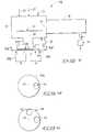
- FIG. 1depicts a first embodiment atomic layer deposition apparatus 10 .
- Suchcomprises an atomic layer deposition chamber 12 having a substrate passageway 14 communicating to externally of the chamber.
- a load chamber 16is in fluid communication with atomic layer deposition chamber 12 through substrate passageway 14 .
- a load chamber vacuum pumpis diagrammatically depicted with numeral 18 , and is in fluid communication with load chamber 16 apart from through substrate passageway 14 .
- Load chamber vacuum pump 18includes an illustrated discharge indicated by a downward arrow, and a by-pass inlet illustrated by a horizontal arrow pointing to the left proximate thereto.
- additional vacuum pumpsmight be associated with load chamber 16 and/or pump 18 could be configured to include a roughing vacuum pump apparatus and a non-roughing vacuum pump apparatus.
- a “roughing vacuum pump”is a vacuum pump (or sub-pumping components/apparatus of a non-roughing vacuum pump) which is configured to provide an initial reduced pressure from at or near atmospheric pressure, and which is used with a non-roughing vacuum pump that further reduces pressure.
- a “non-roughing vacuum pump”is a vacuum pump configured to provide a subatmospheric deposition operating pressure within the chamber.
- atomic layer deposition chamber 12is provided with three gas inlets 20 , 22 and 24 .
- any two of such inletsmight be configured for feeding different deposition precursors to chamber 12 , with the remaining inlet being configured for feeding a purge gas to deposition chamber 12 .
- a first non-roughing vacuum pump 26is in fluid communication with deposition chamber 12 apart from substrate passageway 14 .
- a second non-roughing vacuum pump 28is in fluid communication with deposition chamber 12 apart from substrate passageway 14 .
- Any suitable pumps capable of producing a desired subatmospheric deposition pressureare contemplated whether existing or yet-to-be developed.
- suchinclude turbomolecular pumps, diffusion pumps, sublimation pumps, cryo pumps, diffusion ejector pumps, absorption pumps, sliding-vane rotary pumps, rotary piston pumps, rotary plunger pumps, root pumps, etc.
- a roughing vacuum pump 30is provided in fluid communication with chamber 12 apart from substrate passageway 14 .
- a roughing vacuum pumpmay or may not be utilized, and might alternately comprise a sub-pumping device of non-roughing vacuum pump assemblies. Further, such might be in fluid communication with chamber 12 through a separate line from non-roughing vacuum pumps 26 and 28 (as shown), or through conduits or other gas passageways (not shown) associated with non-roughing vacuum pumps 26 and 28 . Further of course, non-roughing vacuum pumps 26 and 28 could comprise respective multiple pumping devices/components/apparatus (roughing and/or non-roughing) connected in series and/or in parallel.
- the first and second non-roughing vacuum pumpscan be configured to have different rated throughputs over a given operating pressure range. Alternately, the first and second non-roughing vacuum pumps can be configured to have common rated throughputs over a given operating pressure range.
- Second non-roughing vacuum pump 28is depicted as being diagrammatically larger than first non-roughing vacuum pump 26 , thereby having corresponding larger and smaller throughputs, respectively. In such depicted preferred embodiment, second non-roughing vacuum pump 28 is configured with chamber 12 for feeding a purge gas to the chamber, while first non-roughing vacuum pump 26 is configured with chamber 12 for feeding a deposition precursor to the chamber.
- first and second non-roughing vacuum pumps 26 and 28might be configured for operating at variable speeds over a given operating pressure range, or configured for operating at respective constant speeds over a given operating pressure range. Further, one may be configured for operating at a constant speed over a given operating pressure range with the other being configured for operating at variable speeds over a given operating pressure range.
- FIG. 1depicts an embodiment whereby chamber 12 is provided with multiple outlets 32 and 34 , with one of said outlets (outlet 32 ) being in fluid communication with first non-roughing vacuum pump 26 and another of said outlets (outlet 34 ) being in fluid communication with second non-roughing vacuum pump 28 .
- pressure control valving or other apparatuscould be associated with one or more of the illustrated pumps, outlets and/or conduits for controlling the pressure, or isolating one or more pumps from the chamber while one or more other pump(s) operate(s) relative to the chamber.
- by-pass inletsare illustrated by respective horizontal arrows pointing to the right proximate each pump, for example should a pump be isolated from communicating with chamber 12 during operation. Such might be used to minimize transient pressure changes with respect to the feedlines when switching between pumps.
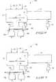
- FIG. 2illustrates an alternate embodiment 10 a .
- Atomic layer deposition apparatus 10 ais provided with one outlet 38 at chamber 12 which is in fluid communication with both first and second non-roughing vacuum pumps 26 a and 28 a, respectively.
- a suitable conduit 40extends from outlet 38 .
- First and second non-roughing vacuum pumps 26 a and 28 a, respectively,are in fluid communication with conduit 40 .
- At least one isolation valveis associated with the illustrated first and second pumps. In the depicted preferred embodiment, there is one and only one such isolation valve diagrammatically depicted as an embodiment 42 . Further in the depicted embodiment, isolation valve assembly 42 is in the form of a pivotable flap valve 44 received within conduit 40 and configured for selectively isolating the first and second pumps 26 a and 28 a, respectively, from fluid communication with conduit 40 .
- FIGS. 3 - 5depict an alternate embodiment atomic layer deposition apparatus 10 b. Like numerals from the first and second described embodiments are utilized where appropriate, with differences being indicated by the suffix “b” or with different numerals.
- Atomic layer deposition apparatus 10 bincludes a rotatable valve 42 b received within conduit 40 b, and which is configured for selectively isolating first and second pumps 26 b and 28 b, respectively, from fluid communication with conduit 40 b.
- Rotatable valve 42 bis depicted in the exemplary embodiment as being mounted for rotation about a central axis 43 .
- a valve opening 46is received radially from axis 43 and can be selectively positioned to provide flow relative to second non-roughing vacuum pump 28 b (as shown), or with respect to first non-roughing vacuum pump 26 b by 180° rotation about axis 43 (not shown).
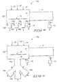
- FIG. 5depicts an exemplary alternate embodiment rotatable valve 48 having two adjacent valve openings 50 and 52 positioned proximate to but radially 90° from one another. This particular exemplary embodiment would enable switching between first non-roughing vacuum pump 26 b and second non-roughing vacuum pump 28 b by 90° rotation as opposed to the 180° of rotation with respect to the 42 b diagrammatic embodiment.
- FIGS. 6 and 7illustrate another alternate embodiment atomic layer deposition apparatus 10 c, and in different respective operational configurations. Like numerals from the above-described embodiments are utilized where appropriate, with differences being indicated with the suffix “c”, or with different numerals.
- Valve assembly 42 cis depicted diagrammatically as a slidable valve received within conduit 40 c and configured for selectively isolating first and second pumps 26 c and 28 c, respectively, from fluid communication with conduit 40 c.
- FIG. 6depicts one operational configuration where valve 42 c is slid to provide fluid communication of pump 26 c with conduit 40 c, while second pump 28 c is restricted from fluid communication with conduit 40 c.
- FIG. 7depicts the opposite.
- FIG. 8illustrates another alternate embodiment atomic layer deposition apparatus 10 d.
- Atomic layer deposition apparatus 10 dcomprises a third non-roughing vacuum pump 60 in fluid communication with chamber 12 d apart from substrate passageway 14 .
- third non-roughing vacuum pump 60is configured with chamber 12 d for feeding a second deposition precursor to chamber 12 d.
- separate precursor feed pumpsi.e., pumps 26 d and 60
- pump 26 d and 60are separately optimized for their respective different deposition precursors (for example, in one or both of materials of construction or designed throughput) while another of the non-roughing vacuum pumps (i.e., pump 28 d ) is configured for feeding a purge gas to the chamber (for example, with respect to desired higher throughput than with the deposition precursors).
- FIG. 8 depicted embodimentshows chamber 12 d as being provided with multiple outlets 32 d , 34 d and 62 , which are in respective fluid communication with first non-roughing vacuum pump 26 d, second non-roughing vacuum pump 28 d and third non-roughing vacuum pump 60 , respectively.
- FIG. 9depicts an alternate embodiment atomic layer deposition apparatus 10 e wherein a chamber 12 e is provided with one outlet 40 e at the chamber. Outlet 40 e is in fluid communication with each of first, second and third non-roughing vacuum pumps 32 e, 34 e and 60 e, respectively. Of course, more than three non-roughing vacuum pumps could be utilized.
- the inventioncontemplates an atomic layer deposition method using the above-described apparatus, and methods independent thereof.
- the concluding apparatus claimsare not limited by the method claims, nor are the concluding method claims limited by any attribute of the apparatus claims, unless literal language appears in such claims and without any limiting or interpretative reference to the specification or drawings.
- the respective method claim families and apparatus claim familiesstand as literally worded without reference to the other.
- An exemplary first embodiment atomic layer deposition method in accordance with the inventionpositions a semiconductor substrate within an atomic layer deposition chamber, for example any of the above-described chambers.
- semiconductor substrateor “semiconductive substrate” is defined to mean any construction comprising semiconductive material, including, but not limited to, bulk semiconductive materials such as a semiconductive wafer (either alone or in assemblies comprising other materials thereon), and semiconductive material layers (either alone or in assemblies comprising other materials).
- substraterefers to any supporting structure, including, but not limited to, the semiconductive substrates described above. Such positioning can occur by passing a substrate 70 to be processed from load chamber 16 through substrate passageway 14 onto a suitable substrate holder (not shown) within atomic layer deposition chamber 12 . A first deposition precursor is fed through the chamber under first vacuum conditions effective to form a first monolayer on the substrate. The first vacuum conditions are maintained, at least in part, by a first non-roughing vacuum pump connected to the chamber and through which at least some of the first deposition precursor flows.
- a purge gasis fed to the chamber under second vacuum conditions maintained, at least in part, by a second non-roughing vacuum pump connected to the chamber, which is different from the first non-roughing vacuum pump, and through which at least some of the purge gas flows.
- a roughing vacuum pumpis utilized to lower chamber pressure prior to feeding the first deposition precursor.
- a second deposition precursoris fed to the chamber effective to form a second monolayer on the first monolayer.
- any existing or yet-to-be developed deposition precursorsare of course contemplated.
- the second deposition precursor feedingmight be conducted under third vacuum conditions effective to form a second monolayer on the first monolayer using the first non-roughing vacuum pump.
- the second deposition precursor feeding to the chambermight be conducted under third vacuum conditions maintained, at least in part, by a third non-roughing vacuum pump connected to the chamber, which is different from the first and second non-roughing vacuum pumps.
- the first vacuum conditionsinclude a substantially constant vacuum pressure within the chamber.
- the first vacuum conditionsinclude varied vacuum pressure within the chamber.
- the vacuum pressure within the chamberis substantially the same under the first and second vacuum conditions, and in a most preferred embodiment, the vacuum pressure is substantially constant within the chamber under the first and second vacuum conditions.
- the vacuum pressure within the chamberis different under the first and second vacuum conditions, and in a sub-embodiment, preferably is both substantially constant during each of the first and second vacuum conditions but different from one another under the first and second vacuum conditions.
- an atomic layer deposition method in accordance with the inventionincludes isolating the first non-roughing vacuum pump from the chamber during at least some of the purge gas feeding.
- the methodincludes isolating the second non-roughing vacuum pump from the chamber during at least some of the first deposition precursor feeding, and in one sub-embodiment, preferably during all of the first deposition precursor feeding.
- the methodcomprises operating the second non-roughing vacuum pump at a higher pumping speed during the purge gas feeding than the first non-roughing vacuum pump is operated at during the first deposition precursor feeding.
Landscapes
- Chemical & Material Sciences (AREA)
- Engineering & Computer Science (AREA)
- Materials Engineering (AREA)
- Chemical Kinetics & Catalysis (AREA)
- Organic Chemistry (AREA)
- Metallurgy (AREA)
- General Chemical & Material Sciences (AREA)
- Mechanical Engineering (AREA)
- Microelectronics & Electronic Packaging (AREA)
- Condensed Matter Physics & Semiconductors (AREA)
- Power Engineering (AREA)
- Crystallography & Structural Chemistry (AREA)
- Physics & Mathematics (AREA)
- General Physics & Mathematics (AREA)
- Computer Hardware Design (AREA)
- Manufacturing & Machinery (AREA)
- Chemical Vapour Deposition (AREA)
Abstract
Description
- This invention relates to atomic layer deposition.[0001]
- Atomic layer deposition involves the deposition of successive monolayers over a substrate within a deposition chamber typically maintained at subatmospheric pressure. An exemplary such method includes feeding a single vaporized precursor to a deposition chamber effective to form a first monolayer over a substrate received therein. Thereafter, the flow of the first deposition precursor is ceased and an inert purge gas is flowed through the chamber effective to remove any remaining first precursor which is not adhering to the substrate from the chamber. Subsequently, a second vapor precursor different from the first is flowed to the chamber effective to form a second monolayer on/with the first monolayer. The second monolayer might react with the first monolayer. Additional precursors can form successive monolayers, or the above process can be repeated until a desired thickness and composition layer has been formed over the substrate.[0002]
- The invention includes improvements in apparatus and methods of atomic layer depositions, whether existing or yet-to-be developed, whereby at least one monolayer is formed over a substrate.[0003]
- The invention includes atomic layer deposition methods and apparatus. In one implementation, an atomic layer deposition method includes positioning a semiconductor substrate within an atomic layer deposition chamber. A first deposition precursor is fed to the chamber under first vacuum conditions effective to form a first monolayer on the substrate. The first vacuum conditions are maintained at least in part by a first non-roughing vacuum pump connected to the chamber and through which at least some of the first deposition precursor flows. After forming the first monolayer, a purge gas is fed to the chamber under second vacuum conditions maintained at least in part by a second non-roughing vacuum pump connected to the chamber which is different from the first non-roughing vacuum pump and through which at least some of the purge gas flows.[0004]
- In one implementation, an atomic layer deposition apparatus includes an atomic layer deposition chamber having a substrate passageway communicating to externally of the chamber. A first non-roughing vacuum pump is in fluid communication with the chamber apart from the substrate passageway. A second non-roughing vacuum pump is in fluid communication with the chamber apart from the substrate passageway.[0005]
- Preferred embodiments of the invention are described below with reference to the following accompanying drawings.[0006]
- FIG. 1 is a diagrammatic depiction of an atomic layer deposition apparatus in accordance with an aspect of the invention.[0007]
- FIG. 2 is a diagrammatic depiction of an atomic layer deposition apparatus in accordance with an aspect of the invention.[0008]
- FIG. 3 is a diagrammatic depiction of an atomic layer deposition apparatus in accordance with an aspect of the invention.[0009]
- FIG. 4 is a sectional view taken through line[0010]4-4 in FIG. 3.
- FIG. 5 is an alternate embodiment sectional view as would be taken through line[0011]4-4 in FIG. 3.
- FIG. 6 is a diagrammatic depiction of an atomic layer deposition apparatus in accordance with an aspect of the invention in a first operational state.[0012]
- FIG. 7 is a view of the FIG. 6 apparatus in a second operational state.[0013]
- FIG. 8 is a diagrammatic depiction of an atomic layer deposition apparatus in accordance with an aspect of the invention.[0014]
- FIG. 9 is a diagrammatic depiction of an atomic layer deposition apparatus in accordance with an aspect of the invention.[0015]
- This disclosure of the invention is submitted in furtherance of the constitutional purposes of the U.S. Patent Laws “to promote the progress of science and useful arts” (Article 1, Section 8).[0016]
- FIG. 1 depicts a first embodiment atomic[0017]
layer deposition apparatus 10. Such comprises an atomic layer deposition chamber12 having asubstrate passageway 14 communicating to externally of the chamber. Aload chamber 16 is in fluid communication with atomic layer deposition chamber12 throughsubstrate passageway 14. A load chamber vacuum pump is diagrammatically depicted withnumeral 18, and is in fluid communication withload chamber 16 apart from throughsubstrate passageway 14. Loadchamber vacuum pump 18 includes an illustrated discharge indicated by a downward arrow, and a by-pass inlet illustrated by a horizontal arrow pointing to the left proximate thereto. In the preferred embodiment, additional vacuum pumps might be associated withload chamber 16 and/orpump 18 could be configured to include a roughing vacuum pump apparatus and a non-roughing vacuum pump apparatus. In the context of this document, a “roughing vacuum pump” is a vacuum pump (or sub-pumping components/apparatus of a non-roughing vacuum pump) which is configured to provide an initial reduced pressure from at or near atmospheric pressure, and which is used with a non-roughing vacuum pump that further reduces pressure. Also in the context of this document, a “non-roughing vacuum pump” is a vacuum pump configured to provide a subatmospheric deposition operating pressure within the chamber. - In the illustrated exemplary embodiment, atomic layer deposition chamber[0018]12 is provided with three
gas inlets - A first[0019]
non-roughing vacuum pump 26 is in fluid communication with deposition chamber12 apart fromsubstrate passageway 14. A secondnon-roughing vacuum pump 28 is in fluid communication with deposition chamber12 apart fromsubstrate passageway 14. Any suitable pumps capable of producing a desired subatmospheric deposition pressure are contemplated whether existing or yet-to-be developed. By way of example only, such include turbomolecular pumps, diffusion pumps, sublimation pumps, cryo pumps, diffusion ejector pumps, absorption pumps, sliding-vane rotary pumps, rotary piston pumps, rotary plunger pumps, root pumps, etc. A roughingvacuum pump 30 is provided in fluid communication with chamber12 apart fromsubstrate passageway 14. As described above with respect to loadchamber vacuum pump 18, a roughing vacuum pump may or may not be utilized, and might alternately comprise a sub-pumping device of non-roughing vacuum pump assemblies. Further, such might be in fluid communication with chamber12 through a separate line fromnon-roughing vacuum pumps 26 and28 (as shown), or through conduits or other gas passageways (not shown) associated withnon-roughing vacuum pumps vacuum pumps - The first and second non-roughing vacuum pumps can be configured to have different rated throughputs over a given operating pressure range. Alternately, the first and second non-roughing vacuum pumps can be configured to have common rated throughputs over a given operating pressure range. Second[0020]
non-roughing vacuum pump 28 is depicted as being diagrammatically larger than firstnon-roughing vacuum pump 26, thereby having corresponding larger and smaller throughputs, respectively. In such depicted preferred embodiment, secondnon-roughing vacuum pump 28 is configured with chamber12 for feeding a purge gas to the chamber, while first non-roughingvacuum pump 26 is configured with chamber12 for feeding a deposition precursor to the chamber. For example, and by way of example only, it might be desirable to draw or feed the purge gas through the system at much higher throughput over a given pressure range than a throughput which would be desired over a given pressure range (under the same or different pressure range) for a deposition precursor. Also, first and secondnon-roughing vacuum pumps - FIG. 1 depicts an embodiment whereby chamber[0021]12 is provided with
multiple outlets non-roughing vacuum pump 26 and another of said outlets (outlet34) being in fluid communication with secondnon-roughing vacuum pump 28. Of course, pressure control valving or other apparatus could be associated with one or more of the illustrated pumps, outlets and/or conduits for controlling the pressure, or isolating one or more pumps from the chamber while one or more other pump(s) operate(s) relative to the chamber. For example, by-pass inlets are illustrated by respective horizontal arrows pointing to the right proximate each pump, for example should a pump be isolated from communicating with chamber12 during operation. Such might be used to minimize transient pressure changes with respect to the feedlines when switching between pumps. - FIG. 2 illustrates an[0022]
alternate embodiment 10a. Like numerals from the first embodiment are utilized where appropriate, with differences being indicated by the suffix “a” or with different numerals. Atomiclayer deposition apparatus 10ais provided with oneoutlet 38 at chamber12 which is in fluid communication with both first and secondnon-roughing vacuum pumps suitable conduit 40 extends fromoutlet 38. First and secondnon-roughing vacuum pumps conduit 40. At least one isolation valve is associated with the illustrated first and second pumps. In the depicted preferred embodiment, there is one and only one such isolation valve diagrammatically depicted as anembodiment 42. Further in the depicted embodiment,isolation valve assembly 42 is in the form of apivotable flap valve 44 received withinconduit 40 and configured for selectively isolating the first andsecond pumps conduit 40. - FIGS.[0023]3-5 depict an alternate embodiment atomic
layer deposition apparatus 10b.Like numerals from the first and second described embodiments are utilized where appropriate, with differences being indicated by the suffix “b” or with different numerals. Atomiclayer deposition apparatus 10bincludes arotatable valve 42breceived withinconduit 40b,and which is configured for selectively isolating first andsecond pumps conduit 40b.Rotatable valve 42bis depicted in the exemplary embodiment as being mounted for rotation about acentral axis 43. Avalve opening 46 is received radially fromaxis 43 and can be selectively positioned to provide flow relative to secondnon-roughing vacuum pump 28b(as shown), or with respect to firstnon-roughing vacuum pump 26bby 180° rotation about axis43 (not shown). - FIG. 5 depicts an exemplary alternate embodiment[0024]
rotatable valve 48 having twoadjacent valve openings non-roughing vacuum pump 26band secondnon-roughing vacuum pump 28bby 90° rotation as opposed to the 180° of rotation with respect to the42bdiagrammatic embodiment. - FIGS. 6 and 7 illustrate another alternate embodiment atomic[0025]
layer deposition apparatus 10c,and in different respective operational configurations. Like numerals from the above-described embodiments are utilized where appropriate, with differences being indicated with the suffix “c”, or with different numerals.Valve assembly 42cis depicted diagrammatically as a slidable valve received withinconduit 40cand configured for selectively isolating first andsecond pumps conduit 40c.FIG. 6 depicts one operational configuration wherevalve 42cis slid to provide fluid communication ofpump 26cwithconduit 40c,whilesecond pump 28cis restricted from fluid communication withconduit 40c.FIG. 7 depicts the opposite. - Of course, any additional or alternate isolating valving assemblies, whether existing or yet-to-be developed, might be utilized.[0026]
- FIG. 8 illustrates another alternate embodiment atomic[0027]
layer deposition apparatus 10d.Like numerals from the above-described embodiments are utilized where appropriate, with differences being indicated with the suffix “d”, or with different numerals. Atomiclayer deposition apparatus 10dcomprises a third non-roughing vacuum pump60 in fluid communication withchamber 12dapart fromsubstrate passageway 14. In one preferred embodiment, third non-roughing vacuum pump60 is configured withchamber 12dfor feeding a second deposition precursor tochamber 12d.For example, in one preferred embodiment, separate precursor feed pumps (i.e., pumps26dand60) are separately optimized for their respective different deposition precursors (for example, in one or both of materials of construction or designed throughput) while another of the non-roughing vacuum pumps (i.e., pump28d) is configured for feeding a purge gas to the chamber (for example, with respect to desired higher throughput than with the deposition precursors). - The FIG. 8 depicted embodiment shows[0028]
chamber 12das being provided withmultiple outlets non-roughing vacuum pump 26d,secondnon-roughing vacuum pump 28dand third non-roughing vacuum pump60, respectively. FIG. 9 depicts an alternate embodiment atomiclayer deposition apparatus 10ewherein achamber 12eis provided with oneoutlet 40eat the chamber.Outlet 40eis in fluid communication with each of first, second and thirdnon-roughing vacuum pumps - The invention contemplates an atomic layer deposition method using the above-described apparatus, and methods independent thereof. In other words, the concluding apparatus claims are not limited by the method claims, nor are the concluding method claims limited by any attribute of the apparatus claims, unless literal language appears in such claims and without any limiting or interpretative reference to the specification or drawings. The respective method claim families and apparatus claim families stand as literally worded without reference to the other. An exemplary first embodiment atomic layer deposition method in accordance with the invention positions a semiconductor substrate within an atomic layer deposition chamber, for example any of the above-described chambers. In the context of this document, the term “semiconductor substrate” or “semiconductive substrate” is defined to mean any construction comprising semiconductive material, including, but not limited to, bulk semiconductive materials such as a semiconductive wafer (either alone or in assemblies comprising other materials thereon), and semiconductive material layers (either alone or in assemblies comprising other materials). The term “substrate” refers to any supporting structure, including, but not limited to, the semiconductive substrates described above. Such positioning can occur by passing a[0029]
substrate 70 to be processed fromload chamber 16 throughsubstrate passageway 14 onto a suitable substrate holder (not shown) within atomic layer deposition chamber12. A first deposition precursor is fed through the chamber under first vacuum conditions effective to form a first monolayer on the substrate. The first vacuum conditions are maintained, at least in part, by a first non-roughing vacuum pump connected to the chamber and through which at least some of the first deposition precursor flows. - After forming the first monolayer, a purge gas is fed to the chamber under second vacuum conditions maintained, at least in part, by a second non-roughing vacuum pump connected to the chamber, which is different from the first non-roughing vacuum pump, and through which at least some of the purge gas flows. In one preferred embodiment, a roughing vacuum pump is utilized to lower chamber pressure prior to feeding the first deposition precursor. In one preferred embodiment, after feeding the purge gas, a second deposition precursor, different from the first deposition precursor, is fed to the chamber effective to form a second monolayer on the first monolayer. In the context of atomic layer deposition, any existing or yet-to-be developed deposition precursors are of course contemplated. The second deposition precursor feeding might be conducted under third vacuum conditions effective to form a second monolayer on the first monolayer using the first non-roughing vacuum pump. Alternately by way of example only, the second deposition precursor feeding to the chamber might be conducted under third vacuum conditions maintained, at least in part, by a third non-roughing vacuum pump connected to the chamber, which is different from the first and second non-roughing vacuum pumps.[0030]
- In one preferred embodiment, the first vacuum conditions include a substantially constant vacuum pressure within the chamber. In another preferred embodiment, the first vacuum conditions include varied vacuum pressure within the chamber. In yet another preferred embodiment, the vacuum pressure within the chamber is substantially the same under the first and second vacuum conditions, and in a most preferred embodiment, the vacuum pressure is substantially constant within the chamber under the first and second vacuum conditions. In another preferred embodiment, the vacuum pressure within the chamber is different under the first and second vacuum conditions, and in a sub-embodiment, preferably is both substantially constant during each of the first and second vacuum conditions but different from one another under the first and second vacuum conditions.[0031]
- In one preferred embodiment, an atomic layer deposition method in accordance with the invention includes isolating the first non-roughing vacuum pump from the chamber during at least some of the purge gas feeding. In another preferred embodiment, the method includes isolating the second non-roughing vacuum pump from the chamber during at least some of the first deposition precursor feeding, and in one sub-embodiment, preferably during all of the first deposition precursor feeding.[0032]
- In one preferred embodiment, the method comprises operating the second non-roughing vacuum pump at a higher pumping speed during the purge gas feeding than the first non-roughing vacuum pump is operated at during the first deposition precursor feeding.[0033]
- In compliance with the statute, the invention has been described in language more or less specific as to structural and methodical features. It is to be understood, however, that the invention is not limited to the specific features shown and described, since the means herein disclosed comprise preferred forms of putting the invention into effect. The invention is, therefore, claimed in any of its forms or modifications within the proper scope of the appended claims appropriately interpreted in accordance with the doctrine of equivalents.[0034]
Claims (53)
Priority Applications (4)
| Application Number | Priority Date | Filing Date | Title |
|---|---|---|---|
| US10/097,025US6893506B2 (en) | 2002-03-11 | 2002-03-11 | Atomic layer deposition apparatus and method |
| US10/741,300US20040129219A1 (en) | 2002-03-11 | 2003-12-17 | Atomic layer deposition apparatus and method |
| US11/055,487US7030037B2 (en) | 2002-03-11 | 2005-02-11 | Atomic layer deposition apparatus and method |
| US11/364,738US7431773B2 (en) | 2002-03-11 | 2006-02-28 | Atomic layer deposition apparatus and method |
Applications Claiming Priority (1)
| Application Number | Priority Date | Filing Date | Title |
|---|---|---|---|
| US10/097,025US6893506B2 (en) | 2002-03-11 | 2002-03-11 | Atomic layer deposition apparatus and method |
Related Child Applications (1)
| Application Number | Title | Priority Date | Filing Date |
|---|---|---|---|
| US10/741,300DivisionUS20040129219A1 (en) | 2002-03-11 | 2003-12-17 | Atomic layer deposition apparatus and method |
Publications (2)
| Publication Number | Publication Date |
|---|---|
| US20030170403A1true US20030170403A1 (en) | 2003-09-11 |
| US6893506B2 US6893506B2 (en) | 2005-05-17 |
Family
ID=27788306
Family Applications (4)
| Application Number | Title | Priority Date | Filing Date |
|---|---|---|---|
| US10/097,025Expired - LifetimeUS6893506B2 (en) | 2002-03-11 | 2002-03-11 | Atomic layer deposition apparatus and method |
| US10/741,300AbandonedUS20040129219A1 (en) | 2002-03-11 | 2003-12-17 | Atomic layer deposition apparatus and method |
| US11/055,487Expired - Fee RelatedUS7030037B2 (en) | 2002-03-11 | 2005-02-11 | Atomic layer deposition apparatus and method |
| US11/364,738Expired - Fee RelatedUS7431773B2 (en) | 2002-03-11 | 2006-02-28 | Atomic layer deposition apparatus and method |
Family Applications After (3)
| Application Number | Title | Priority Date | Filing Date |
|---|---|---|---|
| US10/741,300AbandonedUS20040129219A1 (en) | 2002-03-11 | 2003-12-17 | Atomic layer deposition apparatus and method |
| US11/055,487Expired - Fee RelatedUS7030037B2 (en) | 2002-03-11 | 2005-02-11 | Atomic layer deposition apparatus and method |
| US11/364,738Expired - Fee RelatedUS7431773B2 (en) | 2002-03-11 | 2006-02-28 | Atomic layer deposition apparatus and method |
Country Status (1)
| Country | Link |
|---|---|
| US (4) | US6893506B2 (en) |
Cited By (21)
| Publication number | Priority date | Publication date | Assignee | Title |
|---|---|---|---|---|
| US6852167B2 (en) | 2001-03-01 | 2005-02-08 | Micron Technology, Inc. | Methods, systems, and apparatus for uniform chemical-vapor depositions |
| US7081421B2 (en) | 2004-08-26 | 2006-07-25 | Micron Technology, Inc. | Lanthanide oxide dielectric layer |
| US7084078B2 (en) | 2002-08-29 | 2006-08-01 | Micron Technology, Inc. | Atomic layer deposited lanthanide doped TiOx dielectric films |
| US7135369B2 (en) | 2003-03-31 | 2006-11-14 | Micron Technology, Inc. | Atomic layer deposited ZrAlxOy dielectric layers including Zr4AlO9 |
| US7160577B2 (en) | 2002-05-02 | 2007-01-09 | Micron Technology, Inc. | Methods for atomic-layer deposition of aluminum oxides in integrated circuits |
| US7192824B2 (en) | 2003-06-24 | 2007-03-20 | Micron Technology, Inc. | Lanthanide oxide / hafnium oxide dielectric layers |
| US7192892B2 (en) | 2003-03-04 | 2007-03-20 | Micron Technology, Inc. | Atomic layer deposited dielectric layers |
| WO2007057518A1 (en)* | 2005-11-17 | 2007-05-24 | Beneq Oy | Arrangement in connection with ald reactor |
| US7235501B2 (en) | 2004-12-13 | 2007-06-26 | Micron Technology, Inc. | Lanthanum hafnium oxide dielectrics |
| US7402876B2 (en) | 2002-12-04 | 2008-07-22 | Micron Technology, Inc. | Zr— Sn—Ti—O films |
| US7429515B2 (en) | 2001-12-20 | 2008-09-30 | Micron Technology, Inc. | Low-temperature grown high quality ultra-thin CoTiO3 gate dielectrics |
| US7554161B2 (en) | 2002-06-05 | 2009-06-30 | Micron Technology, Inc. | HfAlO3 films for gate dielectrics |
| US7560793B2 (en) | 2002-05-02 | 2009-07-14 | Micron Technology, Inc. | Atomic layer deposition and conversion |
| US7588988B2 (en) | 2004-08-31 | 2009-09-15 | Micron Technology, Inc. | Method of forming apparatus having oxide films formed using atomic layer deposition |
| US7662729B2 (en) | 2005-04-28 | 2010-02-16 | Micron Technology, Inc. | Atomic layer deposition of a ruthenium layer to a lanthanide oxide dielectric layer |
| US7687409B2 (en) | 2005-03-29 | 2010-03-30 | Micron Technology, Inc. | Atomic layer deposited titanium silicon oxide films |
| US7867919B2 (en) | 2004-08-31 | 2011-01-11 | Micron Technology, Inc. | Method of fabricating an apparatus having a lanthanum-metal oxide dielectric layer |
| US8125038B2 (en) | 2002-07-30 | 2012-02-28 | Micron Technology, Inc. | Nanolaminates of hafnium oxide and zirconium oxide |
| WO2013140021A1 (en)* | 2012-03-23 | 2013-09-26 | Picosun Oy | Atomic layer deposition method and apparatuses |
| JP2016009724A (en)* | 2014-06-23 | 2016-01-18 | 東京エレクトロン株式会社 | Film forming apparatus and film forming method |
| CN108715999A (en)* | 2018-08-07 | 2018-10-30 | 嘉兴科民电子设备技术有限公司 | Apparatus for atomic layer deposition |
Families Citing this family (16)
| Publication number | Priority date | Publication date | Assignee | Title |
|---|---|---|---|---|
| SG114529A1 (en)* | 2001-02-23 | 2005-09-28 | Semiconductor Energy Lab | Method of manufacturing a semiconductor device |
| AUPR412801A0 (en)* | 2001-03-30 | 2001-05-03 | Starpharma Limited | Agent for the prevention and treatment of sexually transmitted disease s - I |
| US6893506B2 (en)* | 2002-03-11 | 2005-05-17 | Micron Technology, Inc. | Atomic layer deposition apparatus and method |
| AU2003253689A1 (en)* | 2002-07-31 | 2004-02-16 | Tokyo Electron Limited | Reduced volume, high conductance process chamber |
| US20040058293A1 (en)* | 2002-08-06 | 2004-03-25 | Tue Nguyen | Assembly line processing system |
| KR100498467B1 (en)* | 2002-12-05 | 2005-07-01 | 삼성전자주식회사 | Apparatus for atomic layer deposition with preventing powder generation in exhaust paths |
| FI119478B (en)* | 2005-04-22 | 2008-11-28 | Beneq Oy | Reactor |
| USD536775S1 (en)* | 2006-01-25 | 2007-02-13 | The Dial Corporation | Vaporizer |
| JP2009544842A (en)* | 2006-07-21 | 2009-12-17 | リンデ・インコーポレーテッド | Method and apparatus for vaporizing and delivering precursor solutions for atomic layer deposition |
| US7692222B2 (en)* | 2006-11-07 | 2010-04-06 | Raytheon Company | Atomic layer deposition in the formation of gate structures for III-V semiconductor |
| US8043430B2 (en)* | 2006-12-20 | 2011-10-25 | Lam Research Corporation | Methods and apparatuses for controlling gas flow conductance in a capacitively-coupled plasma processing chamber |
| US8067061B2 (en) | 2007-10-25 | 2011-11-29 | Asm America, Inc. | Reaction apparatus having multiple adjustable exhaust ports |
| KR100949914B1 (en)* | 2007-11-28 | 2010-03-30 | 주식회사 케이씨텍 | Atomic layer deposition apparatus |
| US10964533B2 (en) | 2018-12-21 | 2021-03-30 | Applied Materials, Inc. | ALD process and hardware with improved purge efficiency |
| TWI867267B (en) | 2021-02-24 | 2024-12-21 | 日商國際電氣股份有限公司 | Substrate processing device, semiconductor device manufacturing method, program and exhaust system |
| CN117646193B (en)* | 2024-01-30 | 2024-03-26 | 辽宁拓邦鸿基半导体材料股份有限公司 | Atomic layer deposition device |
Citations (25)
| Publication number | Priority date | Publication date | Assignee | Title |
|---|---|---|---|---|
| US4058430A (en)* | 1974-11-29 | 1977-11-15 | Tuomo Suntola | Method for producing compound thin films |
| US4793283A (en)* | 1987-12-10 | 1988-12-27 | Sarkozy Robert F | Apparatus for chemical vapor deposition with clean effluent and improved product yield |
| US5000225A (en)* | 1989-11-17 | 1991-03-19 | Applied Materials, Inc. | Low profile, combination throttle/gate valve for a multi-pump chamber |
| US5105853A (en)* | 1989-05-23 | 1992-04-21 | Henry Ehrenberg | Mutiway valve |
| US5242539A (en)* | 1991-04-04 | 1993-09-07 | Hitachi, Ltd. | Plasma treatment method and apparatus |
| US5286296A (en)* | 1991-01-10 | 1994-02-15 | Sony Corporation | Multi-chamber wafer process equipment having plural, physically communicating transfer means |
| US5391260A (en)* | 1992-03-27 | 1995-02-21 | Hitachi, Ltd. | Vacuum processing apparatus |
| US5611863A (en)* | 1994-08-22 | 1997-03-18 | Tokyo Electron Limited | Semiconductor processing apparatus and cleaning method thereof |
| US5746581A (en)* | 1994-06-28 | 1998-05-05 | Ebara Corporation | Method and apparatus for evacuating vacuum system |
| US6037272A (en)* | 1996-08-08 | 2000-03-14 | Samsung Electronics Co., Ltd. | Apparatus and method for low pressure chemical vapor deposition using multiple chambers and vacuum pumps |
| US6206970B1 (en)* | 1997-09-03 | 2001-03-27 | Micron Technology, Inc. | Semiconductor wafer processor, semiconductor processor gas filtering system and semiconductor processing methods |
| US6214120B1 (en)* | 1999-08-27 | 2001-04-10 | Innovac Corporation | High throughput multi-vacuum chamber system for processing wafers and method of processing wafers using the same |
| US6270572B1 (en)* | 1998-08-07 | 2001-08-07 | Samsung Electronics Co., Ltd. | Method for manufacturing thin film using atomic layer deposition |
| US6306247B1 (en)* | 2000-04-19 | 2001-10-23 | Taiwan Semiconductor Manufacturing Company, Ltd | Apparatus and method for preventing etch chamber contamination |
| US6316045B1 (en)* | 2000-04-20 | 2001-11-13 | Alcatel | Method and apparatus for conditioning the atmosphere in a process chamber |
| US6391803B1 (en)* | 2001-06-20 | 2002-05-21 | Samsung Electronics Co., Ltd. | Method of forming silicon containing thin films by atomic layer deposition utilizing trisdimethylaminosilane |
| US6410408B1 (en)* | 2000-08-31 | 2002-06-25 | Matsushita Electric Industrial Co., Ltd. | CVD film formation method |
| US6461436B1 (en)* | 2001-10-15 | 2002-10-08 | Micron Technology, Inc. | Apparatus and process of improving atomic layer deposition chamber performance |
| US6503379B1 (en)* | 2000-05-22 | 2003-01-07 | Basic Research, Inc. | Mobile plating system and method |
| US6511539B1 (en)* | 1999-09-08 | 2003-01-28 | Asm America, Inc. | Apparatus and method for growth of a thin film |
| US6572924B1 (en)* | 1999-11-18 | 2003-06-03 | Asm America, Inc. | Exhaust system for vapor deposition reactor and method of using the same |
| US20030153177A1 (en)* | 2002-02-11 | 2003-08-14 | Applied Materials, Inc. | Variable flow deposition apparatus and method in semiconductor substrate processing |
| US6630201B2 (en)* | 2001-04-05 | 2003-10-07 | Angstron Systems, Inc. | Adsorption process for atomic layer deposition |
| US6635965B1 (en)* | 2001-05-22 | 2003-10-21 | Novellus Systems, Inc. | Method for producing ultra-thin tungsten layers with improved step coverage |
| US6730367B2 (en)* | 2002-03-05 | 2004-05-04 | Micron Technology, Inc. | Atomic layer deposition method with point of use generated reactive gas species |
Family Cites Families (17)
| Publication number | Priority date | Publication date | Assignee | Title |
|---|---|---|---|---|
| US662517A (en)* | 1900-06-28 | 1900-11-27 | James Barlow | Valve. |
| JPS6219582A (en) | 1985-07-19 | 1987-01-28 | Agency Of Ind Science & Technol | Production of gamma-thiobutyrolactone derivative |
| JPS62192582A (en)* | 1986-02-19 | 1987-08-24 | Hitachi Ltd | Vacuum evacuation device |
| JPS6421080A (en)* | 1987-07-17 | 1989-01-24 | Sumitomo Metal Ind | Plasma cvd device |
| JPH01187380A (en)* | 1988-01-19 | 1989-07-26 | Seiko Epson Corp | Vacuum processor |
| JPH01189114A (en)* | 1988-01-25 | 1989-07-28 | Nec Corp | Vapor growth apparatus |
| JPH02220367A (en)* | 1989-02-20 | 1990-09-03 | Furukawa Electric Co Ltd:The | secondary battery |
| US5266296A (en)* | 1991-01-22 | 1993-11-30 | General Chemical Corporation | Cocurrent flow process for the manufacture of sodium sulfite and bisulfite solutions |
| JP3130374B2 (en)* | 1992-06-17 | 2001-01-31 | 株式会社日立製作所 | Method for manufacturing semiconductor device |
| JPH11222678A (en)* | 1998-02-03 | 1999-08-17 | Shimadzu Corp | Film forming device |
| JPH11222677A (en) | 1998-02-03 | 1999-08-17 | Shimadzu Corp | Film forming equipment |
| JP4174941B2 (en)* | 2000-02-03 | 2008-11-05 | 株式会社デンソー | Thin film manufacturing method and thin film manufacturing apparatus |
| US6852167B2 (en)* | 2001-03-01 | 2005-02-08 | Micron Technology, Inc. | Methods, systems, and apparatus for uniform chemical-vapor depositions |
| US6893506B2 (en)* | 2002-03-11 | 2005-05-17 | Micron Technology, Inc. | Atomic layer deposition apparatus and method |
| KR100498467B1 (en)* | 2002-12-05 | 2005-07-01 | 삼성전자주식회사 | Apparatus for atomic layer deposition with preventing powder generation in exhaust paths |
| US20040178175A1 (en)* | 2003-03-12 | 2004-09-16 | Pellin Michael J. | Atomic layer deposition for high temperature superconductor material synthesis |
| US7647886B2 (en)* | 2003-10-15 | 2010-01-19 | Micron Technology, Inc. | Systems for depositing material onto workpieces in reaction chambers and methods for removing byproducts from reaction chambers |
- 2002
- 2002-03-11USUS10/097,025patent/US6893506B2/ennot_activeExpired - Lifetime
- 2003
- 2003-12-17USUS10/741,300patent/US20040129219A1/ennot_activeAbandoned
- 2005
- 2005-02-11USUS11/055,487patent/US7030037B2/ennot_activeExpired - Fee Related
- 2006
- 2006-02-28USUS11/364,738patent/US7431773B2/ennot_activeExpired - Fee Related
Patent Citations (26)
| Publication number | Priority date | Publication date | Assignee | Title |
|---|---|---|---|---|
| US4058430A (en)* | 1974-11-29 | 1977-11-15 | Tuomo Suntola | Method for producing compound thin films |
| US4793283A (en)* | 1987-12-10 | 1988-12-27 | Sarkozy Robert F | Apparatus for chemical vapor deposition with clean effluent and improved product yield |
| US5105853A (en)* | 1989-05-23 | 1992-04-21 | Henry Ehrenberg | Mutiway valve |
| US5000225A (en)* | 1989-11-17 | 1991-03-19 | Applied Materials, Inc. | Low profile, combination throttle/gate valve for a multi-pump chamber |
| US5286296A (en)* | 1991-01-10 | 1994-02-15 | Sony Corporation | Multi-chamber wafer process equipment having plural, physically communicating transfer means |
| US5242539A (en)* | 1991-04-04 | 1993-09-07 | Hitachi, Ltd. | Plasma treatment method and apparatus |
| US5391260A (en)* | 1992-03-27 | 1995-02-21 | Hitachi, Ltd. | Vacuum processing apparatus |
| US5607510A (en)* | 1992-03-27 | 1997-03-04 | Hitachi, Ltd. | Vacuum processing apparatus |
| US5746581A (en)* | 1994-06-28 | 1998-05-05 | Ebara Corporation | Method and apparatus for evacuating vacuum system |
| US5611863A (en)* | 1994-08-22 | 1997-03-18 | Tokyo Electron Limited | Semiconductor processing apparatus and cleaning method thereof |
| US6037272A (en)* | 1996-08-08 | 2000-03-14 | Samsung Electronics Co., Ltd. | Apparatus and method for low pressure chemical vapor deposition using multiple chambers and vacuum pumps |
| US6206970B1 (en)* | 1997-09-03 | 2001-03-27 | Micron Technology, Inc. | Semiconductor wafer processor, semiconductor processor gas filtering system and semiconductor processing methods |
| US6270572B1 (en)* | 1998-08-07 | 2001-08-07 | Samsung Electronics Co., Ltd. | Method for manufacturing thin film using atomic layer deposition |
| US6214120B1 (en)* | 1999-08-27 | 2001-04-10 | Innovac Corporation | High throughput multi-vacuum chamber system for processing wafers and method of processing wafers using the same |
| US6511539B1 (en)* | 1999-09-08 | 2003-01-28 | Asm America, Inc. | Apparatus and method for growth of a thin film |
| US6572924B1 (en)* | 1999-11-18 | 2003-06-03 | Asm America, Inc. | Exhaust system for vapor deposition reactor and method of using the same |
| US6306247B1 (en)* | 2000-04-19 | 2001-10-23 | Taiwan Semiconductor Manufacturing Company, Ltd | Apparatus and method for preventing etch chamber contamination |
| US6316045B1 (en)* | 2000-04-20 | 2001-11-13 | Alcatel | Method and apparatus for conditioning the atmosphere in a process chamber |
| US6503379B1 (en)* | 2000-05-22 | 2003-01-07 | Basic Research, Inc. | Mobile plating system and method |
| US6410408B1 (en)* | 2000-08-31 | 2002-06-25 | Matsushita Electric Industrial Co., Ltd. | CVD film formation method |
| US6630201B2 (en)* | 2001-04-05 | 2003-10-07 | Angstron Systems, Inc. | Adsorption process for atomic layer deposition |
| US6635965B1 (en)* | 2001-05-22 | 2003-10-21 | Novellus Systems, Inc. | Method for producing ultra-thin tungsten layers with improved step coverage |
| US6391803B1 (en)* | 2001-06-20 | 2002-05-21 | Samsung Electronics Co., Ltd. | Method of forming silicon containing thin films by atomic layer deposition utilizing trisdimethylaminosilane |
| US6461436B1 (en)* | 2001-10-15 | 2002-10-08 | Micron Technology, Inc. | Apparatus and process of improving atomic layer deposition chamber performance |
| US20030153177A1 (en)* | 2002-02-11 | 2003-08-14 | Applied Materials, Inc. | Variable flow deposition apparatus and method in semiconductor substrate processing |
| US6730367B2 (en)* | 2002-03-05 | 2004-05-04 | Micron Technology, Inc. | Atomic layer deposition method with point of use generated reactive gas species |
Cited By (36)
| Publication number | Priority date | Publication date | Assignee | Title |
|---|---|---|---|---|
| US7410668B2 (en) | 2001-03-01 | 2008-08-12 | Micron Technology, Inc. | Methods, systems, and apparatus for uniform chemical-vapor depositions |
| US6852167B2 (en) | 2001-03-01 | 2005-02-08 | Micron Technology, Inc. | Methods, systems, and apparatus for uniform chemical-vapor depositions |
| US7429515B2 (en) | 2001-12-20 | 2008-09-30 | Micron Technology, Inc. | Low-temperature grown high quality ultra-thin CoTiO3 gate dielectrics |
| US7589029B2 (en) | 2002-05-02 | 2009-09-15 | Micron Technology, Inc. | Atomic layer deposition and conversion |
| US7560793B2 (en) | 2002-05-02 | 2009-07-14 | Micron Technology, Inc. | Atomic layer deposition and conversion |
| US7670646B2 (en) | 2002-05-02 | 2010-03-02 | Micron Technology, Inc. | Methods for atomic-layer deposition |
| US7160577B2 (en) | 2002-05-02 | 2007-01-09 | Micron Technology, Inc. | Methods for atomic-layer deposition of aluminum oxides in integrated circuits |
| US7554161B2 (en) | 2002-06-05 | 2009-06-30 | Micron Technology, Inc. | HfAlO3 films for gate dielectrics |
| US8125038B2 (en) | 2002-07-30 | 2012-02-28 | Micron Technology, Inc. | Nanolaminates of hafnium oxide and zirconium oxide |
| US7388246B2 (en) | 2002-08-29 | 2008-06-17 | Micron Technology, Inc. | Lanthanide doped TiOx dielectric films |
| US7084078B2 (en) | 2002-08-29 | 2006-08-01 | Micron Technology, Inc. | Atomic layer deposited lanthanide doped TiOx dielectric films |
| US7402876B2 (en) | 2002-12-04 | 2008-07-22 | Micron Technology, Inc. | Zr— Sn—Ti—O films |
| US7410917B2 (en) | 2002-12-04 | 2008-08-12 | Micron Technology, Inc. | Atomic layer deposited Zr-Sn-Ti-O films using TiI4 |
| US7405454B2 (en) | 2003-03-04 | 2008-07-29 | Micron Technology, Inc. | Electronic apparatus with deposited dielectric layers |
| US7192892B2 (en) | 2003-03-04 | 2007-03-20 | Micron Technology, Inc. | Atomic layer deposited dielectric layers |
| US7135369B2 (en) | 2003-03-31 | 2006-11-14 | Micron Technology, Inc. | Atomic layer deposited ZrAlxOy dielectric layers including Zr4AlO9 |
| US7625794B2 (en) | 2003-03-31 | 2009-12-01 | Micron Technology, Inc. | Methods of forming zirconium aluminum oxide |
| US7312494B2 (en) | 2003-06-24 | 2007-12-25 | Micron Technology, Inc. | Lanthanide oxide / hafnium oxide dielectric layers |
| US7192824B2 (en) | 2003-06-24 | 2007-03-20 | Micron Technology, Inc. | Lanthanide oxide / hafnium oxide dielectric layers |
| US7719065B2 (en) | 2004-08-26 | 2010-05-18 | Micron Technology, Inc. | Ruthenium layer for a dielectric layer containing a lanthanide oxide |
| US7081421B2 (en) | 2004-08-26 | 2006-07-25 | Micron Technology, Inc. | Lanthanide oxide dielectric layer |
| US7867919B2 (en) | 2004-08-31 | 2011-01-11 | Micron Technology, Inc. | Method of fabricating an apparatus having a lanthanum-metal oxide dielectric layer |
| US7588988B2 (en) | 2004-08-31 | 2009-09-15 | Micron Technology, Inc. | Method of forming apparatus having oxide films formed using atomic layer deposition |
| US8154066B2 (en) | 2004-08-31 | 2012-04-10 | Micron Technology, Inc. | Titanium aluminum oxide films |
| US7411237B2 (en) | 2004-12-13 | 2008-08-12 | Micron Technology, Inc. | Lanthanum hafnium oxide dielectrics |
| US7235501B2 (en) | 2004-12-13 | 2007-06-26 | Micron Technology, Inc. | Lanthanum hafnium oxide dielectrics |
| US7687409B2 (en) | 2005-03-29 | 2010-03-30 | Micron Technology, Inc. | Atomic layer deposited titanium silicon oxide films |
| US7662729B2 (en) | 2005-04-28 | 2010-02-16 | Micron Technology, Inc. | Atomic layer deposition of a ruthenium layer to a lanthanide oxide dielectric layer |
| EA015231B1 (en)* | 2005-11-17 | 2011-06-30 | Бенек Ой | Arrangement in connection with ald reactor |
| WO2007057518A1 (en)* | 2005-11-17 | 2007-05-24 | Beneq Oy | Arrangement in connection with ald reactor |
| US20090169743A1 (en)* | 2005-11-17 | 2009-07-02 | Beneq Oy | Arrangement in Connection with ALD Reactor |
| WO2013140021A1 (en)* | 2012-03-23 | 2013-09-26 | Picosun Oy | Atomic layer deposition method and apparatuses |
| CN104204290A (en)* | 2012-03-23 | 2014-12-10 | 皮考逊公司 | Atomic layer deposition method and apparatuses |
| US20150307989A1 (en)* | 2012-03-23 | 2015-10-29 | Picosun Oy | Atomic layer deposition method and apparatuses |
| JP2016009724A (en)* | 2014-06-23 | 2016-01-18 | 東京エレクトロン株式会社 | Film forming apparatus and film forming method |
| CN108715999A (en)* | 2018-08-07 | 2018-10-30 | 嘉兴科民电子设备技术有限公司 | Apparatus for atomic layer deposition |
Also Published As
| Publication number | Publication date |
|---|---|
| US20040129219A1 (en) | 2004-07-08 |
| US20050142890A1 (en) | 2005-06-30 |
| US6893506B2 (en) | 2005-05-17 |
| US7431773B2 (en) | 2008-10-07 |
| US7030037B2 (en) | 2006-04-18 |
| US20060144333A1 (en) | 2006-07-06 |
Similar Documents
| Publication | Publication Date | Title |
|---|---|---|
| US6893506B2 (en) | Atomic layer deposition apparatus and method | |
| US7273526B2 (en) | Thin-film deposition apparatus | |
| US6935372B2 (en) | Semiconductor processing reactive precursor valve assembly | |
| US20060175012A1 (en) | Semiconductor fabrication equipment and method for controlling pressure | |
| JP4979763B2 (en) | Vacuum exhaust system | |
| EP0903769B1 (en) | Spatially uniform gas supply and pump configuration for large wafer diameters | |
| US20070218701A1 (en) | Semiconductor-processing apparatus with rotating susceptor | |
| KR101760789B1 (en) | Method for depositing multi-layered layers and/or gradient layers | |
| US20230102839A1 (en) | Showerhead device for semiconductor processing system | |
| JP2007247066A (en) | Semiconductor-processing apparatus with rotating susceptor | |
| KR20050114234A (en) | Methods and apparatus for atomic layer deposition | |
| US20090110826A1 (en) | Reaction apparatus having multiple adjustable exhaust ports | |
| EP1817500A2 (en) | Fore-line preconditioning for vacuum pumps | |
| US11952660B2 (en) | Semiconductor processing chambers and methods for cleaning the same | |
| US8671965B2 (en) | Methods for enhanced fluid delivery on bevel etch applications | |
| CN101665920A (en) | Film deposition apparatus, substrate process apparatus, and turntable | |
| US11244822B2 (en) | Apparatus for manufacturing a thin film and a method therefor | |
| KR20030063413A (en) | Method and device for treating semiconductor substrates | |
| US6896730B2 (en) | Atomic layer deposition apparatus and methods | |
| US12444621B2 (en) | High conductance divert line architecture | |
| WO2024030506A1 (en) | High conductance divert line architecture | |
| JP2007109685A (en) | Compound semiconductor manufacturing apparatus and compound semiconductor manufacturing method | |
| US20190311887A1 (en) | Multizone gas distribution apparatus | |
| CN120020472A (en) | Wafer cooling processing device, method and semiconductor process equipment | |
| JP2004035931A (en) | Transport type sputtering apparatus and transport type sputtering method |
Legal Events
| Date | Code | Title | Description |
|---|---|---|---|
| AS | Assignment | Owner name:MICRON TECHNOLOGY, INC., IDAHO Free format text:ASSIGNMENT OF ASSIGNORS INTEREST;ASSIGNORS:DOAN, TRUNG TRI;SANDHU, GURTEJ S.;REEL/FRAME:012709/0181 Effective date:20020306 | |
| FEPP | Fee payment procedure | Free format text:PAYOR NUMBER ASSIGNED (ORIGINAL EVENT CODE: ASPN); ENTITY STATUS OF PATENT OWNER: LARGE ENTITY | |
| STCF | Information on status: patent grant | Free format text:PATENTED CASE | |
| FPAY | Fee payment | Year of fee payment:4 | |
| FPAY | Fee payment | Year of fee payment:8 | |
| AS | Assignment | Owner name:U.S. BANK NATIONAL ASSOCIATION, AS COLLATERAL AGENT, CALIFORNIA Free format text:SECURITY INTEREST;ASSIGNOR:MICRON TECHNOLOGY, INC.;REEL/FRAME:038669/0001 Effective date:20160426 Owner name:U.S. BANK NATIONAL ASSOCIATION, AS COLLATERAL AGEN Free format text:SECURITY INTEREST;ASSIGNOR:MICRON TECHNOLOGY, INC.;REEL/FRAME:038669/0001 Effective date:20160426 | |
| AS | Assignment | Owner name:MORGAN STANLEY SENIOR FUNDING, INC., AS COLLATERAL AGENT, MARYLAND Free format text:PATENT SECURITY AGREEMENT;ASSIGNOR:MICRON TECHNOLOGY, INC.;REEL/FRAME:038954/0001 Effective date:20160426 Owner name:MORGAN STANLEY SENIOR FUNDING, INC., AS COLLATERAL Free format text:PATENT SECURITY AGREEMENT;ASSIGNOR:MICRON TECHNOLOGY, INC.;REEL/FRAME:038954/0001 Effective date:20160426 | |
| FPAY | Fee payment | Year of fee payment:12 | |
| AS | Assignment | Owner name:U.S. BANK NATIONAL ASSOCIATION, AS COLLATERAL AGENT, CALIFORNIA Free format text:CORRECTIVE ASSIGNMENT TO CORRECT THE REPLACE ERRONEOUSLY FILED PATENT #7358718 WITH THE CORRECT PATENT #7358178 PREVIOUSLY RECORDED ON REEL 038669 FRAME 0001. ASSIGNOR(S) HEREBY CONFIRMS THE SECURITY INTEREST;ASSIGNOR:MICRON TECHNOLOGY, INC.;REEL/FRAME:043079/0001 Effective date:20160426 Owner name:U.S. BANK NATIONAL ASSOCIATION, AS COLLATERAL AGEN Free format text:CORRECTIVE ASSIGNMENT TO CORRECT THE REPLACE ERRONEOUSLY FILED PATENT #7358718 WITH THE CORRECT PATENT #7358178 PREVIOUSLY RECORDED ON REEL 038669 FRAME 0001. ASSIGNOR(S) HEREBY CONFIRMS THE SECURITY INTEREST;ASSIGNOR:MICRON TECHNOLOGY, INC.;REEL/FRAME:043079/0001 Effective date:20160426 | |
| AS | Assignment | Owner name:JPMORGAN CHASE BANK, N.A., AS COLLATERAL AGENT, ILLINOIS Free format text:SECURITY INTEREST;ASSIGNORS:MICRON TECHNOLOGY, INC.;MICRON SEMICONDUCTOR PRODUCTS, INC.;REEL/FRAME:047540/0001 Effective date:20180703 Owner name:JPMORGAN CHASE BANK, N.A., AS COLLATERAL AGENT, IL Free format text:SECURITY INTEREST;ASSIGNORS:MICRON TECHNOLOGY, INC.;MICRON SEMICONDUCTOR PRODUCTS, INC.;REEL/FRAME:047540/0001 Effective date:20180703 | |
| AS | Assignment | Owner name:MICRON TECHNOLOGY, INC., IDAHO Free format text:RELEASE BY SECURED PARTY;ASSIGNOR:U.S. BANK NATIONAL ASSOCIATION, AS COLLATERAL AGENT;REEL/FRAME:047243/0001 Effective date:20180629 | |
| AS | Assignment | Owner name:MICRON TECHNOLOGY, INC., IDAHO Free format text:RELEASE BY SECURED PARTY;ASSIGNOR:MORGAN STANLEY SENIOR FUNDING, INC., AS COLLATERAL AGENT;REEL/FRAME:050937/0001 Effective date:20190731 | |
| AS | Assignment | Owner name:MICRON TECHNOLOGY, INC., IDAHO Free format text:RELEASE BY SECURED PARTY;ASSIGNOR:JPMORGAN CHASE BANK, N.A., AS COLLATERAL AGENT;REEL/FRAME:051028/0001 Effective date:20190731 Owner name:MICRON SEMICONDUCTOR PRODUCTS, INC., IDAHO Free format text:RELEASE BY SECURED PARTY;ASSIGNOR:JPMORGAN CHASE BANK, N.A., AS COLLATERAL AGENT;REEL/FRAME:051028/0001 Effective date:20190731 |