US20030169152A1 - Contactless integrated circuit reader - Google Patents
Contactless integrated circuit readerDownload PDFInfo
- Publication number
- US20030169152A1 US20030169152A1US10/411,008US41100803AUS2003169152A1US 20030169152 A1US20030169152 A1US 20030169152A1US 41100803 AUS41100803 AUS 41100803AUS 2003169152 A1US2003169152 A1US 2003169152A1
- Authority
- US
- United States
- Prior art keywords
- load modulation
- reader
- modulation signal
- signal
- integrated circuit
- Prior art date
- Legal status (The legal status is an assumption and is not a legal conclusion. Google has not performed a legal analysis and makes no representation as to the accuracy of the status listed.)
- Granted
Links
Images


Classifications
- G—PHYSICS
- G06—COMPUTING OR CALCULATING; COUNTING
- G06K—GRAPHICAL DATA READING; PRESENTATION OF DATA; RECORD CARRIERS; HANDLING RECORD CARRIERS
- G06K7/00—Methods or arrangements for sensing record carriers, e.g. for reading patterns
- G06K7/0008—General problems related to the reading of electronic memory record carriers, independent of its reading method, e.g. power transfer
Definitions
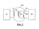
- the present inventionrelates to contactless integrated circuit readers and data transmission by inductive coupling.
- a contactless integrated circuit reader 10 operating by inductive couplingis an active system that sends an alternating magnetic field FLD by means of an antenna circuit 11 and that sends data by modulating the amplitude of the magnetic field sent.
- a contactless integrated circuit 20is a passive device that does not send a magnetic field and comprises an antenna circuit 21 comparable by analogy to the secondary winding of a transformer the primary winding of which would be constituted by the antenna circuit 11 of the reader.
- the magnetic field FLD sent by the readercauses an induced alternating voltage Vac to appear in the antenna circuit of the integrated circuit, said induced voltage copying the amplitude modulations of the magnetic field and enabling the integrated circuit 10 to receive the data sent by the reader, after filtering and demodulating the induced voltage Vac.
- a contactless integrated circuit 20sends data to such a reader by load modulation, i.e. by short-circuiting its antenna circuit by means of a switch driven by a load modulation signal Sx.
- the antenna short-circuitscause a disturbance of the magnetic field FLD that is passed onto the antenna circuit of the reader 10 .
- the lattercan therefore extract the load modulation signal Sx by filtering the signal present in its antenna circuit 11 and deduce the data sent by the contactless integrated circuit from it.
- the antenna circuit of a contactless readeris excited by an alternating signal of a frequency of 13.56 MHz, the data transmission to a contactless integrated circuit is carried out by modulating the amplitude of the magnetic field with a modulating trough of 100% (ISO/A), of 10% (ISO/B) or of 10% to 30% (ISO15).
- the data transmission to a readeris carried out by load modulation by means of a sub-carrier of 847 KHz that is Manchester coded (standard ISO/A) or biphase shit keying (BPSK) coded (standard ISO/B) or by means of a sub-carrier of 423 KHz that is Manchester or frequency shift keying (FSK) coded (IS 0 15).
- a sub-carrier of 847 KHzthat is Manchester coded (standard ISO/A) or biphase shit keying (BPSK) coded (standard ISO/B) or by means of a sub-carrier of 423 KHz that is Manchester or frequency shift keying (FSK) coded (IS 0 15).
- the contactless integrated circuit readersare in the form of fixed terminals.
- these contactless terminalsare capable of recording different pieces of information relating to the operations carried out, which are sometimes necessary to collect to correctly manage the installations.
- an access control terminalis capable of recording each time the door opens, the date, the time and the identity of the badge with which the opening of the door was requested.
- an automatic payment terminalis capable of recording the time of each transaction and the identity of the card with which payment was made.
- this informationit is sometimes desirable for this information to be collected by a data centralization system. To collect the information recorded, it is therefore necessary to provide an infrastructure of electric cables enabling the centralization system to be connected to each of the terminals.
- the reading of the data recorded by a terminalis done manually by means of a terminal reader comprising a connector that is inserted into an output port of the terminal.
- the present inventionaims to overcome this disadvantage.
- one object of the present inventionis to provide a simple means of reading data recorded by a contactless integrated circuit reader.
- one idea of the present inventionis to provide a contactless integrated circuit reader capable of switching to a passive operating mode in which the reader does not send a magnetic field and operates with regard to another reader like a contactless integrated circuit.
- this readeris capable of sending data to another reader according to the load modulation principle, and of receiving data that the other reader sends by modulating the magnetic field it sends out.
- the present inventionit is possible to cause two contactless readers to “converse” or communicate by switching one of the two readers to the passive operating mode. Data can then be exchanged without any mechanical contact between the two readers.
- the first readeris for example a fixed terminal in which data must be read and the second reader is for example a portable reader used to extract the data from the terminal at the end of the day.
- each terminalcan switch to a passive mode to send or receive data to or from a neighbouring terminal, and can therefore be used as a relay for the propagation of data from terminal to terminal.
- another object of the present inventionis to provide a method for transferring data between two readers according to the load modulation principle, that is simple to implement and does not require providing a load modulation switch capable of short-circuiting the antenna circuit of one of the two readers.
- One particular object of the present inventionis to make a contactless integrated circuit reader of the type described in the international applications PCT/FR00/00742 and PCT/FR/00712 operate in passive mode, by minimizing the material modifications to be made to this reader to obtain the desired result.
- another idea of the present inventionis to apply a load modulation signal with two states to the antenna circuit of a first reader, the variations of the signal being capable of disturbing the magnetic field sent by a second reader and of causing the equivalent of a load modulation obtained by short-circuiting the antenna circuit of the first reader in the antenna circuit of the second reader.
- the present inventionprovides an inductive coupling data send-receive device comprising an antenna circuit, means for delivering an alternating signal for exciting the antenna circuit, and means for simulating the operation of a contactless integrated circuit.
- the componentsare arranged for applying a load modulation signal with two states to the antenna circuit when data is to be sent.
- the load modulation signalis capable of disturbing a magnetic field sent by a contactless integrated circuit reader and of being detected by the reader as if it were a load modulation signal sent by a contactless integrated circuit.
- the load modulation signalcomprises pulses of the excitation signal.
- the duration of each pulseis longer than the period of the excitation signal.
- the load modulation signalcomprises groups of pulses of the excitation signal.
- the pulses of a single groupare sent at a determined frequency lower than the frequency of the excitation signal.
- the load modulation signalalternates between the following two states: the logic “0”, i.e. a reference potential, and the high impedance state.
- the load modulation signalalternates between the following two states: the logic “0”, i.e. a reference potential, and the logic “1”, i.e. a direct voltage.
- the load modulation signalis controlled by at least one port of a microprocessor.
- the devicecomprises an active operating mode in which the excitation signal is applied in a substantially constant manner to the antenna circuit and in which data are sent by modulating the amplitude of the magnetic field sent by the antenna circuit.
- the deviceis capable of conversing with a contactless integrated circuit when it is in the active mode.
- the devicealso includes a passive operating mode in which data is sent by applying the load modulation signal with two states to the antenna circuit using the means for simulating the operation of a contactless integrated circuit.
- the deviceis capable of conversing with a contactless integrated circuit reader when it is in the passive mode.
- the means for simulating the operation of a contactless integrated circuitare preferably arranged to inhibit the substantially constant application of the excitation signal to the antenna circuit, at least when the load modulation signal is not applied to the antenna circuit.
- the inhibition of the application of the excitation signal to the antenna circuitis controlled by ports of a microprocessor.
- the devicecomprises means for extracting a load modulation signal sent by a contactless integrated circuit from an antenna signal present in the antenna circuit and means for extracting an amplitude modulation signal sent by a contactless integrated circuit reader from the antenna signal.
- the means for extracting an amplitude modulation signal and the means for extracting a load modulation signalcomprise a common filter circuit linked to the antenna circuit.
- the present inventionalso relates to a method for transferring data between two contactless integrated circuit readers operating by inductive coupling.
- Each readercomprises an antenna circuit for sending an alternating magnetic field, means for applying an alternating excitation signal to the antenna circuit, and means for modulating the amplitude of the magnetic field sent.
- the methodcomprising the steps of providing, at least in a first reader, means for simulating the operation of a contactless integrated circuit and making the first reader operate like a contactless integrated circuit.
- the methodcomprises the steps of applying a load modulation signal to the antenna circuit when data are to be sent, the load modulation signal being capable of disturbing the magnetic field sent by the other reader and of being detected by the other reader, and inhibiting the application of the excitation signal to the antenna circuit at least when the load modulation signal is not applied.
- the load modulation signalcomprises pulses of an alternating signal.
- the duration of each pulseis longer than the period of the alternating signal.
- the load modulation signalcomprises groups of pulses of the excitation signal.
- the pulses of a single groupare sent at a determined frequency lower than the frequency of the excitation signal.
- the load modulation signalalternates between the following two states: the logic “0”, i.e. a reference potential, and the high impedance state.
- the load modulation signalalternates between the following two states: the logic “0”, i.e. a reference potential, and the logic “1”, i.e. a direct voltage.
- the methodcomprises a step of providing filter means in the reader operating like a contactless integrated circuit.
- the filter meansare capable of extracting a load modulation signal sent by a contactless integrated circuit from the antenna signal of the reader and of extracting an amplitude modulation signal sent by the other contactless integrated circuit reader from the antenna signal.
- the present inventionalso relates to a method for sending data to a contactless integrated circuit reader by means of a device comprising an antenna circuit and means for delivering an alternating signal for exciting the antenna circuit.
- the methodcomprises the step of applying a load modulation signal with two states to the antenna circuit.
- the load modulation signalis capable of disturbing a magnetic field sent by a contactless integrated circuit reader and of being detected by the reader as if it were a load modulation signal sent by a contactless integrated circuit.
- the load modulation signalcomprises pulses of the excitation signal.
- the duration of each pulseis longer than the period of the excitation signal.
- the load modulation signalcomprises groups of pulses of the excitation signal.
- the pulses of a single groupare sent at a determined frequency lower than the frequency of the excitation signal.
- the load modulation signalalternates between the following two states: the logic “0”, i.e. a reference potential, and the high impedance state.
- the load modulation signalalternates between the following two states: the logic “0”, i.e. a reference potential, and the logic “1”, i.e. a direct voltage.
- FIG. 1previously described, schematically represents a contactless integrated circuit reader and a contactless integrated circuit
- FIG. 2is the wiring diagram of an example of an embodiment of a reader according to the present invention.
- FIGS. 3A to 3 Dare timing diagrams of electric signals showing the operation of the reader in active mode, during a communication with a contactless integrated circuit
- FIGS. 4A to 4 Eare timing diagrams of electric signals showing the operation of the reader in passive mode, during a communication with another reader.
- FIG. 1is the wiring diagram of a reader RD 1 according to the present invention, initially provided to exchange data with a contactless integrated circuit. Therefore, in terms of its general characteristics, the architecture of the reader RD 1 is in itself well known and is described in the international applications PCT/FR00/00742 and PCT/FR/00712.
- the reader RD 1can be essentially distinguished from the classical reader in that it comprises means for switching to a passive operating mode in which it simulates the operation of a contactless integrated circuit to converse or communicate with another contactless integrated circuit reader.
- the reader RD 1classically comprises a microprocessor MP 1 , a memory MEM 1 , an external antenna circuit LCR 1 , an oscillator OSC 1 , an amplitude modulation circuit MDC 1 and a data extraction circuit EXTC 1 .
- the antenna circuit LCR 1comprises a coil Lr 1 and a capacitor Cr 1 in parallel and has a resonance frequency of about 13.56 MHz.
- the oscillator OSC 1delivers an excitation signal SI of a frequency of about 13.56 MHz that is applied to the antenna circuit LCR 1 through the modulation circuit MDC 1 .
- the signal S 1is also applied to the microprocessor as a clock signal H.
- the microprocessor MP 1is supplied by a direct voltage Vcc and comprises ports P 1 to P 8 that can be set to “0” (ground), to “1” (Vcc) or to the high impedance state (HZ).
- the ports P 1 to P 7are output ports while the port P 8 is an input port.
- the memory MEM 1comprises a non-volatile area, such as a read only memory (ROM) or an electronically erasable programmable read only memory (EEPROM)-type area for example, in which various classical programs are logged, particularly the operating system OS of the microprocessor, a program PGA 1 for managing a protocol to send data by amplitude modulation and a program PGA 2 for managing a protocol to receive data sent by a contactless integrated circuit according to the load modulation principle.
- ROMread only memory
- EEPROMelectronically erasable programmable read only memory
- the memory MEM 1also comprises a program PGP 1 for managing a protocol to receive data sent by another contactless integrated circuit reader (by modulating the amplitude of an external magnetic field), and a program PGP 2 for managing a protocol to send data by load modulation.
- PGP 1for managing a protocol to receive data sent by another contactless integrated circuit reader (by modulating the amplitude of an external magnetic field)
- PGP 2for managing a protocol to send data by load modulation.
- the modulation circuit MDC 1comprises a transistor T 1 , here of the negative-channel metal oxide semiconductor (NMOS) type, the gate of which receives the signal S 1 and the source of which is connected to the ground.
- the drain of the modulation transistor T 1is linked to the antenna circuit LCR 1 through a capacitor C 1 and is linked to the ports P 1 to P 4 of the microprocessor MP 1 through an inductor or “shock” inductor L 1 .
- the signal S 1is applied to the gate of the modulation transistor T 1 through a logic gate LG, here an AND gate, receiving the signal S 1 and a control signal CMD delivered by the output port P 5 of the microprocessor MP 1 .
- the data extraction circuit EXTC 1comprises a band-pass filter BPF 1 set to a frequency of about 847 KHz and a low-pass filter LPF 1 having a cut-off frequency of about 847 KHz.
- the band-pass filter BPF 1comprises for example an inductor, a capacitor, a resistor and a diode in parallel
- the low-pass filter LPF 1comprises a resistor and a capacitor in parallel.
- Each filter BPF 1 , LPF 1is connected by one of its ends to a port P 6 , P 7 of the microprocessor MP 1 , respectively.
- the other end of the filters BPF 1 , LPF 1is connected to a common node N 1 that is connected to the output of an amplifier element T 2 .
- the amplifier element T 2is a transistor T 2 of the FET type, the drain of which is connected to the node N 1 and the source of which is connected to the ground. Furthermore, the node N 1 is linked to the port P 8 of the microprocessor MP 1 through an amplifier AMP 1 and a trigger TRG 1 transforming a signal delivered by the amplifiers BPF 1 , LPF 1 .
- the data extraction circuit EXTC 1also comprises a half-wave rectifier DR 1 and a low-pass filter LPF 2 having a cut-off frequency on the order of about 1 MHz.
- the half-wave rectifier DR 1is connected to the antenna circuit LCR 1 and its output is applied to the input of the low-pass filter LPF 2 .
- the output of the filter LPF 2is applied to the input of the amplifier element T 2 (here the gate of the field-effect transistor FET) through a decoupling capacitor C 2 and a pull-down resistor R 1 .
- the operation of the reader RD 1 in active modeis classical in itself and comprises first of all sending a magnetic field FLD 1 .
- the ports P 1 to P 4 of the microprocessor MP 1are-set to 1 and the signal CMD is set to 1.
- the output of the circuit MDC 1delivers the excitation signal S 1 to the antenna circuit LCR 1 and an antenna signal SA 1 of the same frequency appears in the antenna circuit LCR 1 , causing the magnetic field FLD 1 intended to activate a contactless integrated circuit to be sent.
- the circuit CICcan be an integrated circuit of a contactless smart card, of a contactless electronic badge, of a contactless electronic tag, etc.
- the circuit CICis equipped with an antenna circuit LCP comprising a coil Lp in parallel with a capacitor Cp. It comprises a load modulation switch TM, here an NMOS transistor, a hard-wired logic or microprocessor central processing unit UC, a modulator circuit MODC (the output of which drives the gate of the transistor TM), a data extraction circuit EXTC 3 connected to the antenna circuit LCP, a diode rectifier PD and a frequency divider circuit DWVC.
- the switch TMis connected to the terminals of the antenna circuit LCP through a load resistor RM.
- the magnetic field FLD 1 sent by the reader RD 1causes an induced voltage Vac to appear at the terminals of the coil Lp.
- the voltage Vacis rectified by the diode bridge PD.
- the output of the diode bridge PDdelivers a supply voltage Vcc of the circuit CIC.
- the oscillation frequency of about 13.56 MHz of the voltage Vacis divided by the circuit DIVC, the output of which delivers a sub-carrier Fsc of about 847 KHz sent to the circuit MODC.
- FIGS. 3A to 3 DThe exchange of data between the reader RD 1 and the circuit CIC is shown by FIGS. 3A to 3 D.
- the left-hand side of these figuresrelates to sending data to the circuit CIC (send mode) and the right-hand side relates to receiving data sent by the integrated circuit (receiving mode).
- FIG. 3Ashows an example of data DT to be sent and an example of coding of the signal SM 1 is represented in FIG. 3B.
- this codinginvolves temporarily setting the signal SM 1 to 0 when a 0 is sent, and maintaining the signal SM 1 at 1 when a 1 is sent.
- the change of the signal SM 1 to 0blocks the transistor T 1 in the circuit MDC 1 and extinguishes the antenna signal SA 1 , because the excitation signal S 1 no longer being applied to the antenna circuit LCR 1 .
- the magnetic field FLD 1represented in FIG. 3C, thus has a short amplitude modulation when a bit on 0 is sent and has no amplitude modulation when a bit on 1 is sent (pulse coding).
- the modulation troughis of 100% (ISO/A coding) when all the ports P 1 to P 4 are set to 0 but may also be lower than 100%, such as 10% for example (ISO/B standard), by setting certain ports P 1 to P 4 to the high impedance state HZ while the others remain on 1 (instead of setting all the ports to 0).
- the amplitude modulation signal SM 1is extracted from the induced voltage Vac by the circuit EXTC 3 , and is applied to the central processing unit UC for decoding received data DT.
- the integrated circuitsends data DT (FIG. 3A, right-hand side) to the reader RD 1 .
- Data DTis applied to the circuit MODC to be coded in accordance with the chosen protocol, and the circuit MODC applies a load modulation signal SX 1 to the gate of the transistor TM.
- the signal SX 1is for example the result of Manchester coding applied to the sub-carrier Fsc (standard ISO/A).
- the signal SX 1may also be the result of BPSK coding applied to the sub-carrier Fsc (standard ISO/B).
- the function of the ports P 6 and P 7is to switch the filters BPF 1 , LPF 1 while ensuring their electric power supply.
- the ports P 6 , P 7are on high impedance, the filters BPF 1 , LPF 1 are disconnected (in open circuit) and the node N 1 is at high impedance HZ.
- a port P 6 , P 7is set to 1 while the other port is maintained at high impedance HZ, the corresponding filter BPF 1 , LPF 1 is put into operation.
- the microprocessor MP 1selects and activates the low-pass filter LPF 1 by means of the port P 7 when the signal SX 1 is Manchester coded (standard ISO/A) or selects the band-pass filter BPF 1 by means of port P 6 when the signal SX 1 is BPSK coded.
- the load modulation signal SX 1is first of all extracted from the antenna signal SA 1 by the low-pass filter LPF 2 of the circuit EXTC 1 , which eliminates the component at 13.56 MHz, and is applied to the input of the amplifier element T 2 .
- the filter BPF 1 or LPF 1 selected by means of the ports P 6 , P 7enables the envelope of the signal SX 1 to be extracted, by eliminating the sub-carrier Fsc.
- the envelope of the signal SX 1is sent to the port P 8 of the microprocessor to be decoded, after being amplified by the amplifier AMP 1 and transformed by the trigger TRG 1 .
- the low-pass filter LPF 1enables any type of signal SX 1 the frequency of which is lower than or equal to about 847 KHz to be frequency demodulated, including when the signal, SX 1 is a binary signal without sub-carrier.
- the band-pass filter BPF 1is more particularly dedicated to the phase demodulation of the signal SX 1 when the latter is phase jump coded (BPSK) and has a frequency of about 847 KHz.
- An object of the present inventionis to simulate the operation of a contactless integrated circuit by means of the reader RD 1 , so as to enable data to be exchanged between the reader RD 1 and another contactless integrated circuit reader.
- FIG. 1another reader RD 2 is represented schematically in FIG. 1, opposite the reader RD 1 .
- the reader RD 2is here of the same structure as the reader RD 1 and comprises an antenna circuit LCR 2 made up of a coil Lr 2 and a capacitor Cr 2 , a microprocessor MP 2 , a memory MEM 2 , a modulation circuit MDC 2 , an oscillator OSC 2 delivering an excitation signal S 2 applied to the antenna circuit LCR 2 through the modulation circuit MDC 2 , and a data extraction circuit EXTC 2 connected to the antenna circuit LCR 2 .
- the reader RD 1is switched to passive operating mode here by a bit or flag Bm stored in a register REG 1 the output of which is connected to an input E 1 of the microprocessor MP 1 .
- the value of the flag Bmis detected by polling (cyclic reading of the register) or by interruption.
- the microprocessor MP 1switches to the passive mode when the flag Bm has a determined value, such as “1” for example.
- the value of the flag Bmcan be changed by a switch or a push button (not shown) accessible manually on the box of the reader RD 1 or be modified by the microprocessor MP 1 itself.
- the microprocessor MP 1may for example be programmed to switch to passive mode at certain times of the day or month, corresponding to the reading of data logged in the memory MEM 1 .
- the switching to passive modecan also be initiated in a menu presented to the user in which the two options modes of operation are presented. This embodiment is applicable to portable readers provided to read fixed readers arranged in terminals by going into passive mode.
- the operation of the reader RD 1 in passive modefirst of all results in the absence of sending the magnetic field FLD 1 which is the only permanent magnetic field existing between the readers RD 1 and RD 2 being the magnetic field FLD 2 sent by the reader RD 2 .
- the signal CMDis set to 0 (port P 5 ) and the ports P 1 to P 4 are set to the high impedance state HZ.
- the signal S 1is therefore blocked by the logic gate LG and does not reach the transistor T 1 of the modulation circuit MDC 1 because the gate of transistor T 1 is maintained on 0 by the output of the gate LG.
- the microprocessor MP 1maintains the ports P 1 to P 4 at 0, such that the transistor T 1 also remains blocked independently of the signal applied to its gate.
- FIGS. 4A to 4 EExamples of sending or receiving data in passive mode will now be described in relation with FIGS. 4A to 4 E.
- the left-hand side of these figuresrelates to receiving data by the reader RD 1 and the right-hand side of these figures relates to sending data by the reader RD 1 .
- data sent by the reader RD 2can be read by means of the data extraction circuit EXTC 1 which, due to its structure and its arrangement, is capable of extracting both a load modulation signal sent by a contactless integrated circuit (signal SX 1 described above) and an amplitude modulation signal.
- FIGS. 4A and 4Crespectively represent the magnetic field FLD 2 sent by the reader RD 2 and the antenna signal SA 1 appearing by induction in the antenna circuit LCR 1 of the reader RD 1 .
- FIG. 3Ait can be seen that the amplitude of the field FLD 2 has modulation troughs (of 100% or 10% according to the coding chosen).
- the envelope of the magnetic field FLD 2is the image of the amplitude modulation signal SM 2 (FIG. 4D) applied by the microprocessor MP 2 to its modulation circuit MDC 2 .
- FIG. 4Dthe amplitude modulation signal
- the antenna signal SA 1copies the amplitude variations of the field FLD 2 , such that the envelope of the antenna signal SA 1 is also the modulation signal SM 2 .
- the microprocessor MP 1selects the low-pass filter LPF 1 by setting the port P 7 to “1”.
- the carrier at 13.56 MHzis removed by the filter LPF 2 at the input of the amplifier element T 2 , and any residual frequencies are eliminated by the filter LPF 1 .
- the amplitude modulation signal SM 2is therefore found again on the port P 8 of the microprocessor MP 1 after being transformed by the amplifier AMP 1 and the trigger circuit TRG 1 .
- the microprocessor MP 1decodes the modulation signal SM 2 by means of the program PGP 1 mentioned above, which contains decoding algorithms provided for the contactless integrated circuits, and deduces the data sent by the reader RD 2 from it.
- the object of the present inventionis to cause a load modulation signal SX 2 to appear in the antenna circuit LCR 2 of the reader RD 2 , without having to add a load modulation switch (of the type of switch TM present at the terminals of the antenna circuit of the integrated circuit CIC) in parallel with the antenna circuit LCR 1 of the reader RD 1 .
- the idea of the present inventionis to apply a load modulation signal SX 2 with two states to the antenna circuit LCR 1 by means of the modulation circuit MDC 1 .
- the load modulation signalis capable of causing a disturbance of the magnetic field FLD 2 sent by the reader RD 2 . This disturbance must be passed onto the antenna circuit LCR 2 with sufficient strength to be detected by the data extraction circuit EXTC 2 of the reader RD 2 .
- Table 1 belowdescribes the various states of the output of the circuit MDC 1 according to the control signals CMD and SM 1 applied thereto.
- the signal delivered by the circuit MDC 1is here designated SX 2 to distinguish it from the signal S 1 delivered by the same circuit when the reader is operating in active mode.
- the output statesare referenced “A” to “F” in the left-hand side column.
- three load modulation methods MDC 1can be chosen to cause a disturbance of the magnetic field FLD 2 that can be detected by the reader RD 2 as a load modulation signal.
- the first methodis summarised in Table 2 below and involves alternating the state A and the state B, such that the load modulation signal SX 2 delivered by the circuit MDC 1 comprises an alternation of “0” and “1”.
- the application of a “0” to the antenna circuit LCR 1amounts to connecting the same to the ground GND (through the capacitor C 1 ) or to any reference potential representing the logic “0”.
- the application of a “1” to the antenna circuitamounts to applying (again through the capacitor C 1 ) the direct supply voltage Vcc of the microprocessor MP 1 to the same, or any other direct voltage representing the logic “1”.
- the second methodis summarized in Table 3 below and involves alternating the state A and the state C, such that the load modulation signal SX 2 delivered by the circuit MDC 1 comprises an alternation between the state “0” (ground or reference potential) and the high impedance state HZ.
- the application of the high impedance state HZamounts to putting the antenna circuit LCR 1 into an open circuit condition.
- the third methodis summarized in Table 4 below and involves alternating the state D and the state E such that the load modulation signal SX 2 delivered by the circuit MDC 1 comprises an alternation between the state “0” (ground) and the alternating excitation state of the antenna circuit LCR 1 by means of the signal S 1 delivered by the oscillator OSC 1 .
- the third methodhas the advantage of offering a maximum communication distance that is clearly greater than the first two methods, as the alternating signal pulses S 1 applied to the antenna circuit LCR 1 cause magnetic field pulses FLD 1 to be sent which are detected by the reader RD 2 at a greater distance than disturbances due to a passive load modulation.
- the disturbance of the magnetic field obtained according to the third methodcan be qualified as “pseudo active load modulation” due to the sending of the alternating magnetic field pulses.
- This third methodtherefore constitutes the preferred embodiment of the present invention, although the other methods are not however excluded from the present invention.
- FIG. 4Brepresents the aspect of the signal SX 2 when data are sent in accordance with Manchester coding and by applying the third load modulation method.
- Sending a “1”results in a series of pulses I 1 , 12 . . . followed by an absence of pulses and sending a “0” results in an absence of pulses followed by a series of pulses I 1 , 12 . . . I 4 etc. (I 1 -I 4 ).
- the pulses I 1 -I 4are sent at the frequency of 847 KHz (load modulation sub-carrier), calculated by the microprocessor MP 1 by division of the clock signal H (signal S 1 ).
- Each pulse I 1 -I 4is constituted by a series of alternations of the signal S 1 .
- FIG. 4Cwhich represents the antenna signal SA 1 , demonstrates that the effect of the application of each pulse I 1 -I 4 to the antenna circuit LCR 1 is to increase the amplitude of the antenna signal SA 1 , which corresponds to sending a magnetic field FLD 1 pulse.
- the antenna signal SA 1comprises a combination of the excitation signal S 1 sent by the oscillator OSC 1 (predominant) and of an induced signal S 2 ′ (negligible before S 1 ) that is the image of the excitation signal S 2 sent by the oscillator OSC 2 of the reader RD 2 .
- the antenna signal SA 1is formed solely by the induced signal S 2 ′ and its amplitude depends on the rate of inductive coupling between the two readers.
- the pulses I 1 -I 4are passed onto the antenna circuit of the reader RD 2 and are extracted by the circuit EXTC 2 , which delivers the signal SX 2 ′ represented in FIG. 4E to the microprocessor MP 2 .
- the signal SX 2 ′is the envelope of the signal SX 2 (i.e. the envelope of the pulses I 1 -I 4 after filtering the component S 1 at 13.56 MHz) and is equivalent to a classical load modulation signal, such as the signal SX 1 represented in FIG. 3D for example.
- the signal SX 2 ′is decoded by the microprocessor MP 2 , which deduces the data DT sent by the reader RD 1 therefrom.
- a reader according to the present inventionmay be provided to operate in passive mode in accordance with any other communication protocol based on the load modulation principle, particularly the protocol ISO 1569 mentioned in the preamble.
- a reader according to the present inventionmay also be provided to operate exclusively in passive mode. In this case, it is no longer a “reader” within the conventional meaning of the term but a device provided to read data in a contactless integrated circuit reader, which is neither a contactless integrated circuit reader nor a contactless integrated circuit (due to its ability to generate an alternating magnetic field).
- a reader according to the present inventionstops sending a magnetic field when it switches to passive mode
- a magnetic fieldcould, however, be sent outside periods of sending data (i.e. the periods of applying the load modulation signal with two states SX 2 ).
- sending a magnetic fieldseems to be unnecessary when the reader is operating in passive mode and conversing with another reader.
- a reader or a device according to the present inventionmay be used in different applications, particularly in the field of reading data logged by contactless readers arranged in fixed terminals.
Landscapes
- Engineering & Computer Science (AREA)
- Artificial Intelligence (AREA)
- Computer Vision & Pattern Recognition (AREA)
- Physics & Mathematics (AREA)
- General Physics & Mathematics (AREA)
- Theoretical Computer Science (AREA)
- Near-Field Transmission Systems (AREA)
- Semiconductor Integrated Circuits (AREA)
- Wire Bonding (AREA)
- Coupling Device And Connection With Printed Circuit (AREA)
- Hard Magnetic Materials (AREA)
Abstract
Description
- This application is a continuation of International Application No. PCT/FR01/03078, filed Oct. 5, 2001, the disclosure of which is incorporated herein by reference.[0001]
- The present invention relates to contactless integrated circuit readers and data transmission by inductive coupling.[0002]
- As represented schematically in FIG. 1, a contactless[0003]
integrated circuit reader 10 operating by inductive coupling is an active system that sends an alternating magnetic field FLD by means of anantenna circuit 11 and that sends data by modulating the amplitude of the magnetic field sent. Conversely, a contactless integratedcircuit 20 is a passive device that does not send a magnetic field and comprises anantenna circuit 21 comparable by analogy to the secondary winding of a transformer the primary winding of which would be constituted by theantenna circuit 11 of the reader. The magnetic field FLD sent by the reader causes an induced alternating voltage Vac to appear in the antenna circuit of the integrated circuit, said induced voltage copying the amplitude modulations of the magnetic field and enabling the integratedcircuit 10 to receive the data sent by the reader, after filtering and demodulating the induced voltage Vac. Furthermore, a contactless integratedcircuit 20 sends data to such a reader by load modulation, i.e. by short-circuiting its antenna circuit by means of a switch driven by a load modulation signal Sx. The antenna short-circuits cause a disturbance of the magnetic field FLD that is passed onto the antenna circuit of thereader 10. The latter can therefore extract the load modulation signal Sx by filtering the signal present in itsantenna circuit 11 and deduce the data sent by the contactless integrated circuit from it. - With reference for example to the ISO standards 14443-2/A or 14443-2/B or ISO 1569, designated hereafter “ISO/A”, “ISO/B” and “ISO15”, the antenna circuit of a contactless reader is excited by an alternating signal of a frequency of 13.56 MHz, the data transmission to a contactless integrated circuit is carried out by modulating the amplitude of the magnetic field with a modulating trough of 100% (ISO/A), of 10% (ISO/B) or of 10% to 30% (ISO15). The data transmission to a reader is carried out by load modulation by means of a sub-carrier of 847 KHz that is Manchester coded (standard ISO/A) or biphase shit keying (BPSK) coded (standard ISO/B) or by means of a sub-carrier of 423 KHz that is Manchester or frequency shift keying (FSK) coded (IS[0004]015).
- The applications of this data transmission technique by inductive coupling are currently increasing, particularly in the fields of electronic payment and access control (smart cards and electronic badges) and in product identification (electronic tags). The contactless integrated circuits are arranged on portable supports (plastic cards, tag supports) having an antenna coil integrated therein. The antenna coil is sometimes integrated directly into the silicon wafer of the integrated circuits (“coil on chip”), in so-called “proximity” applications in which the maximum distance of communication is short and on the order of a few millimetres.[0005]
- In many applications, the contactless integrated circuit readers are in the form of fixed terminals. However, these contactless terminals are capable of recording different pieces of information relating to the operations carried out, which are sometimes necessary to collect to correctly manage the installations. Thus, an access control terminal is capable of recording each time the door opens, the date, the time and the identity of the badge with which the opening of the door was requested. Similarly, an automatic payment terminal is capable of recording the time of each transaction and the identity of the card with which payment was made. In the applications that involve several terminals, it is sometimes desirable for this information to be collected by a data centralization system. To collect the information recorded, it is therefore necessary to provide an infrastructure of electric cables enabling the centralization system to be connected to each of the terminals. In other applications, the reading of the data recorded by a terminal is done manually by means of a terminal reader comprising a connector that is inserted into an output port of the terminal.[0006]
- These various operations of reading data in fixed terminals prove to be tedious when they are done manually or costly when they require an infrastructure of electric cables.[0007]
- The present invention aims to overcome this disadvantage.[0008]
- More particularly, one object of the present invention is to provide a simple means of reading data recorded by a contactless integrated circuit reader.[0009]
- To achieve this object, one idea of the present invention is to provide a contactless integrated circuit reader capable of switching to a passive operating mode in which the reader does not send a magnetic field and operates with regard to another reader like a contactless integrated circuit. In other terms, this reader is capable of sending data to another reader according to the load modulation principle, and of receiving data that the other reader sends by modulating the magnetic field it sends out.[0010]
- Because of the present invention, it is possible to cause two contactless readers to “converse” or communicate by switching one of the two readers to the passive operating mode. Data can then be exchanged without any mechanical contact between the two readers. The first reader is for example a fixed terminal in which data must be read and the second reader is for example a portable reader used to extract the data from the terminal at the end of the day.[0011]
- Furthermore, in applications in which several terminals are close to each other, each terminal can switch to a passive mode to send or receive data to or from a neighbouring terminal, and can therefore be used as a relay for the propagation of data from terminal to terminal.[0012]
- In this context, another object of the present invention is to provide a method for transferring data between two readers according to the load modulation principle, that is simple to implement and does not require providing a load modulation switch capable of short-circuiting the antenna circuit of one of the two readers.[0013]
- One particular object of the present invention is to make a contactless integrated circuit reader of the type described in the international applications PCT/FR00/00742 and PCT/FR/00712 operate in passive mode, by minimizing the material modifications to be made to this reader to obtain the desired result.[0014]
- For that purpose, another idea of the present invention is to apply a load modulation signal with two states to the antenna circuit of a first reader, the variations of the signal being capable of disturbing the magnetic field sent by a second reader and of causing the equivalent of a load modulation obtained by short-circuiting the antenna circuit of the first reader in the antenna circuit of the second reader.[0015]
- Therefore, the present invention provides an inductive coupling data send-receive device comprising an antenna circuit, means for delivering an alternating signal for exciting the antenna circuit, and means for simulating the operation of a contactless integrated circuit. The components are arranged for applying a load modulation signal with two states to the antenna circuit when data is to be sent. The load modulation signal is capable of disturbing a magnetic field sent by a contactless integrated circuit reader and of being detected by the reader as if it were a load modulation signal sent by a contactless integrated circuit.[0016]
- According to one embodiment, the load modulation signal comprises pulses of the excitation signal. The duration of each pulse is longer than the period of the excitation signal.[0017]
- According to another embodiment, the load modulation signal comprises groups of pulses of the excitation signal. The pulses of a single group are sent at a determined frequency lower than the frequency of the excitation signal.[0018]
- According to another embodiment, the load modulation signal alternates between the following two states: the logic “0”, i.e. a reference potential, and the high impedance state.[0019]
- According to another embodiment, the load modulation signal alternates between the following two states: the logic “0”, i.e. a reference potential, and the logic “1”, i.e. a direct voltage.[0020]
- According to another embodiment, the load modulation signal is controlled by at least one port of a microprocessor.[0021]
- According to another embodiment, the device comprises an active operating mode in which the excitation signal is applied in a substantially constant manner to the antenna circuit and in which data are sent by modulating the amplitude of the magnetic field sent by the antenna circuit. The device is capable of conversing with a contactless integrated circuit when it is in the active mode. The device also includes a passive operating mode in which data is sent by applying the load modulation signal with two states to the antenna circuit using the means for simulating the operation of a contactless integrated circuit. The device is capable of conversing with a contactless integrated circuit reader when it is in the passive mode.[0022]
- In passive operating mode, the means for simulating the operation of a contactless integrated circuit are preferably arranged to inhibit the substantially constant application of the excitation signal to the antenna circuit, at least when the load modulation signal is not applied to the antenna circuit.[0023]
- According to another embodiment, the inhibition of the application of the excitation signal to the antenna circuit is controlled by ports of a microprocessor.[0024]
- According to another embodiment, the device comprises means for extracting a load modulation signal sent by a contactless integrated circuit from an antenna signal present in the antenna circuit and means for extracting an amplitude modulation signal sent by a contactless integrated circuit reader from the antenna signal.[0025]
- According to another embodiment, the means for extracting an amplitude modulation signal and the means for extracting a load modulation signal comprise a common filter circuit linked to the antenna circuit.[0026]
- The present invention also relates to a method for transferring data between two contactless integrated circuit readers operating by inductive coupling. Each reader comprises an antenna circuit for sending an alternating magnetic field, means for applying an alternating excitation signal to the antenna circuit, and means for modulating the amplitude of the magnetic field sent. The method comprising the steps of providing, at least in a first reader, means for simulating the operation of a contactless integrated circuit and making the first reader operate like a contactless integrated circuit.[0027]
- According to another embodiment, the method comprises the steps of applying a load modulation signal to the antenna circuit when data are to be sent, the load modulation signal being capable of disturbing the magnetic field sent by the other reader and of being detected by the other reader, and inhibiting the application of the excitation signal to the antenna circuit at least when the load modulation signal is not applied.[0028]
- According to another embodiment, the load modulation signal comprises pulses of an alternating signal. The duration of each pulse is longer than the period of the alternating signal.[0029]
- According to another embodiment, the load modulation signal comprises groups of pulses of the excitation signal. The pulses of a single group are sent at a determined frequency lower than the frequency of the excitation signal.[0030]
- According to another embodiment, the load modulation signal alternates between the following two states: the logic “0”, i.e. a reference potential, and the high impedance state.[0031]
- According to another embodiment, the load modulation signal alternates between the following two states: the logic “0”, i.e. a reference potential, and the logic “1”, i.e. a direct voltage.[0032]
- According to another embodiment, the method comprises a step of providing filter means in the reader operating like a contactless integrated circuit. The filter means are capable of extracting a load modulation signal sent by a contactless integrated circuit from the antenna signal of the reader and of extracting an amplitude modulation signal sent by the other contactless integrated circuit reader from the antenna signal.[0033]
- The present invention also relates to a method for sending data to a contactless integrated circuit reader by means of a device comprising an antenna circuit and means for delivering an alternating signal for exciting the antenna circuit. The method comprises the step of applying a load modulation signal with two states to the antenna circuit. The load modulation signal is capable of disturbing a magnetic field sent by a contactless integrated circuit reader and of being detected by the reader as if it were a load modulation signal sent by a contactless integrated circuit.[0034]
- According to another embodiment, the load modulation signal comprises pulses of the excitation signal. The duration of each pulse is longer than the period of the excitation signal.[0035]
- According to another embodiment, the load modulation signal comprises groups of pulses of the excitation signal. The pulses of a single group are sent at a determined frequency lower than the frequency of the excitation signal.[0036]
- According to another embodiment, the load modulation signal alternates between the following two states: the logic “0”, i.e. a reference potential, and the high impedance state.[0037]
- According to another embodiment, the load modulation signal alternates between the following two states: the logic “0”, i.e. a reference potential, and the logic “1”, i.e. a direct voltage.[0038]
- The foregoing summary, as well as the following detailed description of preferred embodiments of the invention, will be better understood when read in conjunction with the appended drawings. For the purpose of illustrating the invention, there are shown in the drawings embodiments which are presently preferred. It should be understood, however, that the invention is not limited to the precise arrangements and instrumentalities shown.[0039]
- In the drawings:[0040]
- FIG. 1, previously described, schematically represents a contactless integrated circuit reader and a contactless integrated circuit;[0041]
- FIG. 2 is the wiring diagram of an example of an embodiment of a reader according to the present invention;[0042]
- FIGS. 3A to[0043]3D are timing diagrams of electric signals showing the operation of the reader in active mode, during a communication with a contactless integrated circuit; and
- FIGS. 4A to[0044]4E are timing diagrams of electric signals showing the operation of the reader in passive mode, during a communication with another reader.
- FIG. 1 is the wiring diagram of a reader RD[0045]1 according to the present invention, initially provided to exchange data with a contactless integrated circuit. Therefore, in terms of its general characteristics, the architecture of the reader RD1 is in itself well known and is described in the international applications PCT/FR00/00742 and PCT/FR/00712.
- The reader RD[0046]1 can be essentially distinguished from the classical reader in that it comprises means for switching to a passive operating mode in which it simulates the operation of a contactless integrated circuit to converse or communicate with another contactless integrated circuit reader.
- In the following description, the reader RD[0047]1 will be described, without limitation, with reference to the standards ISO/A and ISO/B, the characteristics of which were set forth in the Background of the Invention section. Thus, the filter cut-off frequencies, the signal oscillation frequencies and the coding protocols mentioned below are only given as examples.
- The reader RD[0048]1 classically comprises a microprocessor MP1, a memory MEM1, an external antenna circuit LCR1, an oscillator OSC1, an amplitude modulation circuit MDC1 and a data extraction circuit EXTC1. The antenna circuit LCR1 comprises a coil Lr1 and a capacitor Cr1 in parallel and has a resonance frequency of about 13.56 MHz. The oscillator OSC1 delivers an excitation signal SI of a frequency of about 13.56 MHz that is applied to the antenna circuit LCR1 through the modulation circuit MDC1. The signal S1 is also applied to the microprocessor as a clock signal H.
- The microprocessor MP[0049]1 is supplied by a direct voltage Vcc and comprises ports P1 to P8 that can be set to “0” (ground), to “1” (Vcc) or to the high impedance state (HZ). Here, the ports P1 to P7 are output ports while the port P8 is an input port.
- The memory MEM[0050]1 comprises a non-volatile area, such as a read only memory (ROM) or an electronically erasable programmable read only memory (EEPROM)-type area for example, in which various classical programs are logged, particularly the operating system OS of the microprocessor, a program PGA1 for managing a protocol to send data by amplitude modulation and a program PGA2 for managing a protocol to receive data sent by a contactless integrated circuit according to the load modulation principle.
- According to the present invention, the memory MEM[0051]1 also comprises a program PGP1 for managing a protocol to receive data sent by another contactless integrated circuit reader (by modulating the amplitude of an external magnetic field), and a program PGP2 for managing a protocol to send data by load modulation. These programs enable the reader RD1 to operate in passive mode and use data send-receive protocols provided for contactless integrated circuits.
- The modulation circuit MDC[0052]1 comprises a transistor T1, here of the negative-channel metal oxide semiconductor (NMOS) type, the gate of which receives the signal S1 and the source of which is connected to the ground. The drain of the modulation transistor T1 is linked to the antenna circuit LCR1 through a capacitor C1 and is linked to the ports P1 to P4 of the microprocessor MP1 through an inductor or “shock” inductor L1. According to the present invention, the signal S1 is applied to the gate of the modulation transistor T1 through a logic gate LG, here an AND gate, receiving the signal S1 and a control signal CMD delivered by the output port P5 of the microprocessor MP1.
- The data extraction circuit EXTC[0053]1 comprises a band-pass filter BPF1 set to a frequency of about 847 KHz and a low-pass filter LPF1 having a cut-off frequency of about 847 KHz. The band-pass filter BPF1 comprises for example an inductor, a capacitor, a resistor and a diode in parallel, and the low-pass filter LPF1 comprises a resistor and a capacitor in parallel. Each filter BPF1, LPF1 is connected by one of its ends to a port P6, P7 of the microprocessor MP1, respectively. The other end of the filters BPF1, LPF1 is connected to a common node N1 that is connected to the output of an amplifier element T2. The amplifier element T2, as shown here, is a transistor T2 of the FET type, the drain of which is connected to the node N1 and the source of which is connected to the ground. Furthermore, the node N1 is linked to the port P8 of the microprocessor MP1 through an amplifier AMP1 and a trigger TRG1 transforming a signal delivered by the amplifiers BPF1, LPF1. The data extraction circuit EXTC1 also comprises a half-wave rectifier DR1 and a low-pass filter LPF2 having a cut-off frequency on the order of about 1 MHz. The half-wave rectifier DR1 is connected to the antenna circuit LCR1 and its output is applied to the input of the low-pass filter LPF2. The output of the filter LPF2 is applied to the input of the amplifier element T2 (here the gate of the field-effect transistor FET) through a decoupling capacitor C2 and a pull-down resistor R1.
- The operation of the reader RD[0054]1 in active mode and the operation of the reader in passive mode will be described hereinafter.
- Operation in Active Mode:[0055]
- The operation of the reader RD[0056]1 in active mode is classical in itself and comprises first of all sending a magnetic field FLD1. The ports P1 to P4 of the microprocessor MP1 are-set to 1 and the signal CMD is set to 1. The output of the circuit MDC1 delivers the excitation signal S1 to the antenna circuit LCR1 and an antenna signal SA1 of the same frequency appears in the antenna circuit LCR1, causing the magnetic field FLD1 intended to activate a contactless integrated circuit to be sent.
- An exemplary contactless integrated circuit CIC is represented as in FIG. 1 opposite the reader RD[0057]1. The circuit CIC can be an integrated circuit of a contactless smart card, of a contactless electronic badge, of a contactless electronic tag, etc. The circuit CIC is equipped with an antenna circuit LCP comprising a coil Lp in parallel with a capacitor Cp. It comprises a load modulation switch TM, here an NMOS transistor, a hard-wired logic or microprocessor central processing unit UC, a modulator circuit MODC (the output of which drives the gate of the transistor TM), a data extraction circuit EXTC3 connected to the antenna circuit LCP, a diode rectifier PD and a frequency divider circuit DWVC. The switch TM is connected to the terminals of the antenna circuit LCP through a load resistor RM.
- The magnetic field FLD[0058]1 sent by the reader RD1 causes an induced voltage Vac to appear at the terminals of the coil Lp. The voltage Vac is rectified by the diode bridge PD. The output of the diode bridge PD delivers a supply voltage Vcc of the circuit CIC. Moreover, the oscillation frequency of about 13.56 MHz of the voltage Vac is divided by the circuit DIVC, the output of which delivers a sub-carrier Fsc of about 847 KHz sent to the circuit MODC.
- The exchange of data between the reader RD[0059]1 and the circuit CIC is shown by FIGS. 3A to3D. The left-hand side of these figures relates to sending data to the circuit CIC (send mode) and the right-hand side relates to receiving data sent by the integrated circuit (receiving mode).
- A—Sending Data to the Integrated Circuit:[0060]
- When data DT is to be sent to the circuit CIC, the microprocessor MP[0061]1 of the reader RD1 delivers an amplitude modulation signal SM1 coded according to a determined protocol by means of the ports P1 to P4. FIG. 3A, shows an example of data DT to be sent and an example of coding of the signal SM1 is represented in FIG. 3B. Classically, this coding involves temporarily setting the signal SM1 to 0 when a 0 is sent, and maintaining the signal SM1 at 1 when a 1 is sent. The change of the signal SM1 to 0 blocks the transistor T1 in the circuit MDC1 and extinguishes the antenna signal SA1, because the excitation signal S1 no longer being applied to the antenna circuit LCR1. The magnetic field FLD1, represented in FIG. 3C, thus has a short amplitude modulation when a bit on 0 is sent and has no amplitude modulation when a bit on 1 is sent (pulse coding). As described in the applications PCT/FR00/00742 and PCT/FR/00712, the modulation trough is of 100% (ISO/A coding) when all the ports P1 to P4 are set to 0 but may also be lower than 100%, such as 10% for example (ISO/B standard), by setting certain ports P1 to P4 to the high impedance state HZ while the others remain on 1 (instead of setting all the ports to 0).
- In the circuit CIC, the amplitude modulation signal SM[0062]1 is extracted from the induced voltage Vac by the circuit EXTC3, and is applied to the central processing unit UC for decoding received data DT.
- B—Receiving Data Sent by the Integrated Circuit:[0063]
- It will be assumed here that the integrated circuit sends data DT (FIG. 3A, right-hand side) to the reader RD[0064]1. Data DT is applied to the circuit MODC to be coded in accordance with the chosen protocol, and the circuit MODC applies a load modulation signal SX1 to the gate of the transistor TM. As represented in FIG. 3D, the signal SX1 is for example the result of Manchester coding applied to the sub-carrier Fsc (standard ISO/A). The signal SX1 may also be the result of BPSK coding applied to the sub-carrier Fsc (standard ISO/B).
- In the reader RD[0065]1, the function of the ports P6 and P7 is to switch the filters BPF1, LPF1 while ensuring their electric power supply. When the ports P6, P7 are on high impedance, the filters BPF1, LPF1 are disconnected (in open circuit) and the node N1 is at high impedance HZ. When a port P6, P7 is set to 1 while the other port is maintained at high impedance HZ, the corresponding filter BPF1, LPF1 is put into operation. Therefore, the microprocessor MP1 selects and activates the low-pass filter LPF1 by means of the port P7 when the signal SX1 is Manchester coded (standard ISO/A) or selects the band-pass filter BPF1 by means of port P6 when the signal SX1 is BPSK coded.
- The load modulation signal SX[0066]1 is first of all extracted from the antenna signal SA1 by the low-pass filter LPF2 of the circuit EXTC1, which eliminates the component at 13.56 MHz, and is applied to the input of the amplifier element T2. The filter BPF1 or LPF1 selected by means of the ports P6, P7 enables the envelope of the signal SX1 to be extracted, by eliminating the sub-carrier Fsc. The envelope of the signal SX1 is sent to the port P8 of the microprocessor to be decoded, after being amplified by the amplifier AMP1 and transformed by the trigger TRG1.
- Generally speaking, the low-pass filter LPF[0067]1 enables any type of signal SX1 the frequency of which is lower than or equal to about 847 KHz to be frequency demodulated, including when the signal, SX1 is a binary signal without sub-carrier. The band-pass filter BPF1 is more particularly dedicated to the phase demodulation of the signal SX1 when the latter is phase jump coded (BPSK) and has a frequency of about 847 KHz.
- Operation in Passive Mode:[0068]
- An object of the present invention is to simulate the operation of a contactless integrated circuit by means of the reader RD[0069]1, so as to enable data to be exchanged between the reader RD1 and another contactless integrated circuit reader.
- As an example, another reader RD[0070]2 is represented schematically in FIG. 1, opposite the reader RD1. The reader RD2 is here of the same structure as the reader RD1 and comprises an antenna circuit LCR2 made up of a coil Lr2 and a capacitor Cr2, a microprocessor MP2, a memory MEM2, a modulation circuit MDC2, an oscillator OSC2 delivering an excitation signal S2 applied to the antenna circuit LCR2 through the modulation circuit MDC2, and a data extraction circuit EXTC2 connected to the antenna circuit LCR2.
- The reader RD[0071]1 is switched to passive operating mode here by a bit or flag Bm stored in a register REG1 the output of which is connected to an input E1 of the microprocessor MP1. The value of the flag Bm is detected by polling (cyclic reading of the register) or by interruption. The microprocessor MP1 switches to the passive mode when the flag Bm has a determined value, such as “1” for example. In practice, the value of the flag Bm can be changed by a switch or a push button (not shown) accessible manually on the box of the reader RD1 or be modified by the microprocessor MP1 itself. The microprocessor MP1 may for example be programmed to switch to passive mode at certain times of the day or month, corresponding to the reading of data logged in the memory MEM1. The switching to passive mode can also be initiated in a menu presented to the user in which the two options modes of operation are presented. This embodiment is applicable to portable readers provided to read fixed readers arranged in terminals by going into passive mode.
- The operation of the reader RD[0072]1 in passive mode first of all results in the absence of sending the magnetic field FLD1 which is the only permanent magnetic field existing between the readers RD1 and RD2 being the magnetic field FLD2 sent by the reader RD2. To make the antenna circuit LCR1 of the reader RD1 “silent”, the signal CMD is set to 0 (port P5) and the ports P1 to P4 are set to the high impedance state HZ. The signal S1 is therefore blocked by the logic gate LG and does not reach the transistor T1 of the modulation circuit MDC1 because the gate of transistor T1 is maintained on 0 by the output of the gate LG. In one variation, the microprocessor MP1 maintains the ports P1 to P4 at 0, such that the transistor T1 also remains blocked independently of the signal applied to its gate.
- Examples of sending or receiving data in passive mode will now be described in relation with FIGS. 4A to[0073]4E. The left-hand side of these figures relates to receiving data by the reader RD1 and the right-hand side of these figures relates to sending data by the reader RD1.
- A—Receiving Data by the Reader RD[0074]1:
- Advantageously, data sent by the reader RD[0075]2 can be read by means of the data extraction circuit EXTC1 which, due to its structure and its arrangement, is capable of extracting both a load modulation signal sent by a contactless integrated circuit (signal SX1 described above) and an amplitude modulation signal.
- This can be seen by observing FIGS. 4A and 4C, which respectively represent the magnetic field FLD[0076]2 sent by the reader RD2 and the antenna signal SA1 appearing by induction in the antenna circuit LCR1 of the reader RD1. In FIG. 3A, it can be seen that the amplitude of the field FLD2 has modulation troughs (of 100% or 10% according to the coding chosen). The envelope of the magnetic field FLD2 is the image of the amplitude modulation signal SM2 (FIG. 4D) applied by the microprocessor MP2 to its modulation circuit MDC2. In FIG. 4C, it can be seen that the antenna signal SA1 copies the amplitude variations of the field FLD2, such that the envelope of the antenna signal SA1 is also the modulation signal SM2. To extract the envelope of the antenna signal SA1, the microprocessor MP1 selects the low-pass filter LPF1 by setting the port P7 to “1”. The carrier at 13.56 MHz is removed by the filter LPF2 at the input of the amplifier element T2, and any residual frequencies are eliminated by the filter LPF1. The amplitude modulation signal SM2 is therefore found again on the port P8 of the microprocessor MP1 after being transformed by the amplifier AMP1 and the trigger circuit TRG1.
- The microprocessor MP[0077]1 decodes the modulation signal SM2 by means of the program PGP1 mentioned above, which contains decoding algorithms provided for the contactless integrated circuits, and deduces the data sent by the reader RD2 from it.
- B—Sending Data to the Reader RD[0078]2 by Load Modulation:
- Here, the object of the present invention is to cause a load modulation signal SX[0079]2 to appear in the antenna circuit LCR2 of the reader RD2, without having to add a load modulation switch (of the type of switch TM present at the terminals of the antenna circuit of the integrated circuit CIC) in parallel with the antenna circuit LCR1 of the reader RD1.
- For that purpose, the idea of the present invention is to apply a load modulation signal SX[0080]2 with two states to the antenna circuit LCR1 by means of the modulation circuit MDC1. The load modulation signal is capable of causing a disturbance of the magnetic field FLD2 sent by the reader RD2. This disturbance must be passed onto the antenna circuit LCR2 with sufficient strength to be detected by the data extraction circuit EXTC2 of the reader RD2.
- Table 1 below describes the various states of the output of the circuit MDC[0081]1 according to the control signals CMD and SM1 applied thereto. The signal delivered by the circuit MDC1 is here designated SX2 to distinguish it from the signal S1 delivered by the same circuit when the reader is operating in active mode. The output states are referenced “A” to “F” in the left-hand side column. According to the findings and experiments conducted by the applicant, three load modulation methods MDC1 can be chosen to cause a disturbance of the magnetic field FLD2 that can be detected by the reader RD2 as a load modulation signal.
- The first method is summarised in Table 2 below and involves alternating the state A and the state B, such that the load modulation signal SX[0082]2 delivered by the circuit MDC1 comprises an alternation of “0” and “1”. From an electrical point of view, the application of a “0” to the antenna circuit LCR1 amounts to connecting the same to the ground GND (through the capacitor C1) or to any reference potential representing the logic “0”. The application of a “1” to the antenna circuit amounts to applying (again through the capacitor C1) the direct supply voltage Vcc of the microprocessor MP1 to the same, or any other direct voltage representing the logic “1”.
- The second method is summarized in Table 3 below and involves alternating the state A and the state C, such that the load modulation signal SX[0083]2 delivered by the circuit MDC1 comprises an alternation between the state “0” (ground or reference potential) and the high impedance state HZ. The application of the high impedance state HZ amounts to putting the antenna circuit LCR1 into an open circuit condition.
- The third method is summarized in Table[0084]4 below and involves alternating the state D and the state E such that the load modulation signal SX2 delivered by the circuit MDC1 comprises an alternation between the state “0” (ground) and the alternating excitation state of the antenna circuit LCR1 by means of the signal S1 delivered by the oscillator OSC1.
TABLE 1 modulation possibilities offered by the circuit MDC1 Signal SX2 delivered by the circuit State CMD SM1 MDC1 A 0 0 0 B 0 1 1 C 0 HZ HZ D 1 0 0 E 1 1 S1 (13.56 MHz) F 1 HZ HZ - [0085]
TABLE 2 (charge modulation-method 1) State CMD SM1 SX2 A 0 0 0 B 0 1 1 - [0086]
TABLE 3 (charge modulation-method 2) State CMD SM1 SX2 A 0 0 0 C 0 HZ HZ - [0087]
TABLE 4 (charge modulation-method 3) State CMD SM1 SX2 D 1 0 0 E 1 1 S1 (13.56 MHz) - According to tests conducted by the applicant, these three methods cause a disturbing signal to appear in the antenna circuit LCR[0088]2 of the reader RD2 which is detected by the data extraction circuit EXTC2 of the reader RD2 and which, after filtering of its component at about 13.56 MHz by the extraction circuit EXTC2, gives a signal SX2′ that is equivalent to a classical load modulation signal.
- The third method has the advantage of offering a maximum communication distance that is clearly greater than the first two methods, as the alternating signal pulses S[0089]1 applied to the antenna circuit LCR1 cause magnetic field pulses FLD1 to be sent which are detected by the reader RD2 at a greater distance than disturbances due to a passive load modulation. By comparison with a classical load modulation, which is purely passive, the disturbance of the magnetic field obtained according to the third method can be qualified as “pseudo active load modulation” due to the sending of the alternating magnetic field pulses. This third method therefore constitutes the preferred embodiment of the present invention, although the other methods are not however excluded from the present invention.
- Furthermore, it can be seen in Table 4 that the delivery of a load modulation signal SX[0090]2 comprising an alternation of “0” and of pulses of the signal S1, does not require the control signal CMD to be set to 0. The logic gate LG can therefore be removed in this embodiment and the signal S1 can be constantly applied to the gate of the modulation transistor T1.
- FIG. 4B represents the aspect of the signal SX[0091]2 when data are sent in accordance with Manchester coding and by applying the third load modulation method. Sending a “1” results in a series of pulses I1,12 . . . followed by an absence of pulses and sending a “0” results in an absence of pulses followed by a series of pulses I1,12 . . . I4 etc. (I1-I4). The pulses I1-I4 are sent at the frequency of 847 KHz (load modulation sub-carrier), calculated by the microprocessor MP1 by division of the clock signal H (signal S1). Each pulse I1-I4 is constituted by a series of alternations of the signal S1.
- FIG. 4C, which represents the antenna signal SA[0092]1, demonstrates that the effect of the application of each pulse I1-I4 to the antenna circuit LCR1 is to increase the amplitude of the antenna signal SA1, which corresponds to sending a magnetic field FLD1 pulse. While pulses I1-I4 are being sent, the antenna signal SA1 comprises a combination of the excitation signal S1 sent by the oscillator OSC1 (predominant) and of an induced signal S2′ (negligible before S1) that is the image of the excitation signal S2 sent by the oscillator OSC2 of the reader RD2. Outside periods of sending pulses, the antenna signal SA1 is formed solely by the induced signal S2′ and its amplitude depends on the rate of inductive coupling between the two readers.
- The pulses I[0093]1-I4 are passed onto the antenna circuit of the reader RD2 and are extracted by the circuit EXTC2, which delivers the signal SX2′ represented in FIG. 4E to the microprocessor MP2. The signal SX2′ is the envelope of the signal SX2 (i.e. the envelope of the pulses I1-I4 after filtering the component S1 at 13.56 MHz) and is equivalent to a classical load modulation signal, such as the signal SX1 represented in FIG. 3D for example. The signal SX2′ is decoded by the microprocessor MP2, which deduces the data DT sent by the reader RD1 therefrom.
- It will be understood by those skilled in the art that different variations and embodiments of this reader according to the present invention may be implemented. Although reference has been made above to the ISO standards 14443-2/A or 14443-2/B, a reader according to the present invention may be provided to operate in passive mode in accordance with any other communication protocol based on the load modulation principle, particularly the protocol ISO 1569 mentioned in the preamble. A reader according to the present invention may also be provided to operate exclusively in passive mode. In this case, it is no longer a “reader” within the conventional meaning of the term but a device provided to read data in a contactless integrated circuit reader, which is neither a contactless integrated circuit reader nor a contactless integrated circuit (due to its ability to generate an alternating magnetic field). Moreover, although above it was indicated that a reader according to the present invention stops sending a magnetic field when it switches to passive mode, a magnetic field could, however, be sent outside periods of sending data (i.e. the periods of applying the load modulation signal with two states SX[0094]2). However, in practice, sending a magnetic field seems to be unnecessary when the reader is operating in passive mode and conversing with another reader.
- Therefore, a reader or a device according to the present invention may be used in different applications, particularly in the field of reading data logged by contactless readers arranged in fixed terminals.[0095]
- It will be appreciated by those skilled in the art that changes could be made to the embodiments described above without departing from the broad inventive concept thereof. It is understood, therefore, that this invention is not limited to the particular embodiments disclosed, but it is intended to cover modifications within the spirit and scope of the present invention as defined by the appended claims.[0096]
Claims (23)
Applications Claiming Priority (3)
| Application Number | Priority Date | Filing Date | Title |
|---|---|---|---|
| FR0013198AFR2815490B1 (en) | 2000-10-16 | 2000-10-16 | CONTACTLESS INTEGRATED CIRCUIT READER |
| FR0013198 | 2000-10-16 | ||
| PCT/FR2001/003078WO2002033644A1 (en) | 2000-10-16 | 2001-10-05 | Contact-free integrated circuit reader |
Related Parent Applications (1)
| Application Number | Title | Priority Date | Filing Date |
|---|---|---|---|
| PCT/FR2001/003078ContinuationWO2002033644A1 (en) | 2000-10-16 | 2001-10-05 | Contact-free integrated circuit reader |
Publications (2)
| Publication Number | Publication Date |
|---|---|
| US20030169152A1true US20030169152A1 (en) | 2003-09-11 |
| US7098770B2 US7098770B2 (en) | 2006-08-29 |
Family
ID=8855365
Family Applications (1)
| Application Number | Title | Priority Date | Filing Date |
|---|---|---|---|
| US10/411,008Expired - LifetimeUS7098770B2 (en) | 2000-10-16 | 2003-04-10 | Contactless integrated circuit reader |
Country Status (8)
| Country | Link |
|---|---|
| US (1) | US7098770B2 (en) |
| EP (1) | EP1327222B1 (en) |
| CN (1) | CN1248146C (en) |
| AT (1) | ATE265714T1 (en) |
| AU (1) | AU2001293958A1 (en) |
| DE (1) | DE60103079C5 (en) |
| FR (1) | FR2815490B1 (en) |
| WO (1) | WO2002033644A1 (en) |
Cited By (17)
| Publication number | Priority date | Publication date | Assignee | Title |
|---|---|---|---|---|
| US20050158010A1 (en)* | 2004-01-19 | 2005-07-21 | Masayuki Ikeda | Electronic device and wireless communication terminal |
| US20060027655A1 (en)* | 2004-07-15 | 2006-02-09 | Patrick Smets | Method and system for conducting contactless payment card transactions |
| US20060208066A1 (en)* | 2003-11-17 | 2006-09-21 | Dpd Patent Trust | RFID token with multiple interface controller |
| US20060219776A1 (en)* | 2003-11-17 | 2006-10-05 | Dpd Patent Trust | Rfid reader with multiple interfaces |
| US20060245402A1 (en)* | 2002-12-17 | 2006-11-02 | Sony Corporation | Communication system, communication apparatus, and communication method |
| US20070045418A1 (en)* | 2005-08-23 | 2007-03-01 | Inside Contactless | Inductive coupling reader comprising means for extracting a power supply voltage |
| US20080014867A1 (en)* | 2004-11-16 | 2008-01-17 | Advanced Microelectronic And Automation Technology Ltd. | Portable Identity Card Reader System For Physical and Logical Access |
| US20080204240A1 (en)* | 2005-01-25 | 2008-08-28 | Nxp B.V. | Sensor Circuit Array, A Control Device For Operating A Sensor Circuit Array And A Sensor System |
| US20090040022A1 (en)* | 2004-06-28 | 2009-02-12 | Klaus Finkenzeller | Transponder Unit |
| US20090166421A1 (en)* | 2006-02-15 | 2009-07-02 | Dpd Patent Trust Ltd | Rfid reader / card combination to convert a contact smartcard reader to contactless |
| US20090203313A1 (en)* | 2006-05-05 | 2009-08-13 | Inside Contactless | Method and device for transmitting data by charge modulation |
| US20090206165A1 (en)* | 2008-02-15 | 2009-08-20 | Infineon Technologies Ag | Contactless chip module, contactless device, contactless system, and method for contactless communication |
| US20100117800A1 (en)* | 2007-03-23 | 2010-05-13 | Yong Li | Integrated circuit card and method for transmitting data by radio communication thereof |
| US20100130273A1 (en)* | 2007-03-29 | 2010-05-27 | Kyocera Corporation | Portable wireless device |
| US20160337006A1 (en)* | 2012-01-03 | 2016-11-17 | Inside Secure | Communication method between a dual interface nfc card inserted into an nfc terminal, and an nfc device |
| EP2348603B1 (en)* | 2009-12-24 | 2017-01-25 | Samsung Electronics Co., Ltd. | Wireless power transmission device and method |
| US20230216595A1 (en)* | 2005-04-28 | 2023-07-06 | Otsuka Pharmaceutical Co., Ltd. | Pharma-informatics system |
Families Citing this family (56)
| Publication number | Priority date | Publication date | Assignee | Title |
|---|---|---|---|---|
| GB2362070B (en)* | 2000-05-05 | 2004-06-16 | Nokia Mobile Phones Ltd | Communication devices and method of communication |
| DE60126999T2 (en)* | 2001-05-14 | 2007-11-08 | Innovision Research & Technology Plc, Cirencester | A portable communication device |
| JP2004215225A (en)* | 2002-12-17 | 2004-07-29 | Sony Corp | Communication system, communication method, and data processing device |
| US7088145B2 (en)* | 2002-12-23 | 2006-08-08 | 3M Innovative Properties Company | AC powered logic circuitry |
| CA2533029C (en)* | 2003-07-22 | 2014-06-03 | Nokia Corporation | Reader device for radio frequency identification transponder with transponder functionality |
| US7078937B2 (en)* | 2003-12-17 | 2006-07-18 | 3M Innovative Properties Company | Logic circuitry powered by partially rectified ac waveform |
| WO2005081183A1 (en) | 2004-01-23 | 2005-09-01 | Nokia Corporation | Method, device and system for automated context information based selective data provision by identification means |
| ATE435469T1 (en)* | 2004-03-17 | 2009-07-15 | Nokia Corp | CONTINUOUS DATA PROVISION THROUGH HIGH FREQUENCY IDENTIFICATION (RFID) TRANSPONDER |
| CN1918585B (en) | 2004-03-19 | 2010-05-05 | 诺基亚公司 | Detector logic and radio identification device and method for enhanced terminal operation |
| GB0501115D0 (en)* | 2005-01-19 | 2005-02-23 | Innovision Res & Tech Plc | Combined power coupling and rf communication apparatus |
| TWI301699B (en)* | 2005-10-18 | 2008-10-01 | Sunplus Technology Co Ltd | Transmitting circuit, receiving circuit, interface switching module and interface switching method for sata and sas interface |
| DE102005061660A1 (en)* | 2005-12-22 | 2007-06-28 | Giesecke & Devrient Gmbh | Portable data carrier with active contactless interface |
| FR2901077B1 (en)* | 2006-05-10 | 2008-07-11 | Inside Contactless Sa | METHOD FOR ROUTING INPUT AND OUTGOING DATA IN AN NFC CHIP SET |
| EP1855229B1 (en) | 2006-05-10 | 2010-08-11 | Inside Contactless | Method of routing input and output data in an NFC chipset |
| US7920046B1 (en) | 2006-07-21 | 2011-04-05 | Impinj, Inc. | RFID readers and systems initializing after antenna switch and methods |
| US8120494B1 (en) | 2006-07-21 | 2012-02-21 | Impinj, Inc. | RFID readers and systems with antenna switching upon detecting too few tags and methods |
| FR2911706B1 (en)* | 2007-01-23 | 2009-04-03 | Affiliated Comp Services Solut | STORING DATA EXCHANGED BETWEEN AN ELECTRONIC CIRCUIT AND A READING AND / OR WRITING SYSTEM. |
| FR2913550A1 (en) | 2007-03-07 | 2008-09-12 | Inside Contactless Sa | METHOD FOR SECURELY LOADING ACCESS DATA TO A SERVICE IN AN NFC CHIPSET |
| US8451098B2 (en)* | 2007-08-05 | 2013-05-28 | Intel Corporation | Switchable active-passive RFID tag |
| FR2921739B1 (en)* | 2007-09-27 | 2010-05-14 | Inside Contactless | METHOD AND APPARATUS FOR MANAGING APPLICATION DATA IN AN NFC SYSTEM IN RESPONSE TO NON-CONTACT DATA TRANSMISSION OR RECEPTION |
| ATE532138T1 (en) | 2007-09-27 | 2011-11-15 | Inside Secure | METHOD AND DEVICE FOR MANAGING APPLICATION DATA IN AN NFC SYSTEM IN RESPONSE TO SENDING OR RECEIVING DATA WITHOUT CONTACT |
| FR2921738B1 (en)* | 2007-09-27 | 2010-05-14 | Inside Contactless | METHOD AND APPARATUS FOR MANAGING INTERNAL APPLICATION DATA IN AN NFC SYSTEM |
| US9460440B2 (en)* | 2008-02-21 | 2016-10-04 | The Coca-Cola Company | Systems and methods for providing electronic transaction auditing and accountability |
| US8645273B2 (en)* | 2008-02-21 | 2014-02-04 | The Coca-Cola Company | Systems and methods for providing a vending network |
| US20090216665A1 (en)* | 2008-02-21 | 2009-08-27 | The Coca-Cola Company | Systems and Methods for Providing Vending Network Data Management |
| US20090216675A1 (en)* | 2008-02-21 | 2009-08-27 | The Coca-Cola Company | Commission Centric Network Operation Systems and Methods |
| US8121917B2 (en) | 2008-03-03 | 2012-02-21 | The Coca-Cola Company | Systems for implementing a loyalty program |
| US20090222339A1 (en)* | 2008-03-03 | 2009-09-03 | The Coca-Cola Company | Systems and Methods for Providing a Personal Terminal for a Loyalty Program |
| US20090222300A1 (en)* | 2008-03-03 | 2009-09-03 | The Coca-Cola Company | Systems and Methods of Marketing to Defined Consumer Groups |
| US8015088B2 (en)* | 2008-03-03 | 2011-09-06 | The Coca-Cola Company | Methods for implementing a loyalty program |
| EP2107694A1 (en) | 2008-03-31 | 2009-10-07 | STMicroelectronics (Rousset) SAS | Terminal for radiofrequency transmission-reception by means of inductive coupling |
| EP2177922A1 (en) | 2008-10-15 | 2010-04-21 | Gemalto SA | Method for testing an electronic identity document and corresponding device |
| EP2363825B1 (en) | 2010-03-04 | 2016-04-27 | Inside Secure | Method for conducting a transaction by means of an NFC device |
| FR2962571B1 (en) | 2010-07-08 | 2012-08-17 | Inside Contactless | METHOD FOR PERFORMING A SECURE APPLICATION IN AN NFC DEVICE |
| CA2752609C (en) | 2010-09-21 | 2018-08-14 | Inside Secure | Nfc card for portable device |
| FR2965082B1 (en)* | 2010-09-21 | 2012-09-28 | Inside Contactless | METHOD AND DEVICE FOR INDUCTIVE COUPLING ACTIVATED LOAD MODULATION |
| EP2431927B1 (en) | 2010-09-21 | 2018-07-04 | Inside Secure | Eddy currents sensitive NFC card |
| SI23786A (en) | 2011-06-29 | 2012-12-31 | Ids D.O.O. | Procedure and circuit for high-frequency communication between questioner and a smart label |
| FR2985343B1 (en) | 2012-01-03 | 2014-01-03 | Inside Secure | METHOD FOR EXECUTING AN APPLICATION IN AN NFC DEVICE |
| FR2986928B1 (en)* | 2012-02-09 | 2014-09-19 | Inside Secure | SPEAKER FOR MOBILE TELEPHONE COMPRISING AN NFC DEVICE |
| US9331378B2 (en)* | 2012-05-29 | 2016-05-03 | Nxp B.V. | Active load modulation antenna |
| FR2996328B1 (en) | 2012-09-28 | 2015-09-11 | Inside Secure | METHOD FOR PROTECTING SENSITIVE DATA TRANSMITTED IN AN NFC SYSTEM |
| FR2998121B1 (en) | 2012-11-14 | 2014-11-21 | Inside Secure | NFC DEVICE COMPRISING CONFIGURABLE NOTIFICATION MEANS |
| WO2014121928A1 (en)* | 2013-02-07 | 2014-08-14 | Giesecke & Devrient Gmbh | Method and device for testing a circuit |
| KR102072522B1 (en) | 2013-03-07 | 2020-02-03 | 삼성전자주식회사 | Contactless communication device and user device including the same |
| FR3010817B1 (en) | 2013-09-13 | 2016-12-23 | Inside Secure | METHOD AND DEVICE FOR DATA TRANSMISSION BY CONTROLLED AUTO-OSCILLATION INDUCTIVE COUPLING |
| DE102013114135A1 (en)* | 2013-12-16 | 2015-06-18 | Endress + Hauser Conducta Gesellschaft für Mess- und Regeltechnik mbH + Co. KG | Electronic circuit for generating an ASK signal and measuring system |
| EP3160165B1 (en) | 2015-10-22 | 2018-08-15 | Panthronics AG | Nfc "split stack" architecture |
| US10019608B2 (en) | 2015-12-09 | 2018-07-10 | Nxp B.V. | Method and device for phase calibration with active load modulation |
| US10756881B2 (en) | 2016-08-01 | 2020-08-25 | Nxp B.V. | Method and system for operating a communications device that communicates via inductive coupling |
| US9935689B2 (en) | 2016-08-01 | 2018-04-03 | Nxp B.V. | Method and system to measure the phase offset based on the frequency response in a NFC system |
| US10567092B2 (en)* | 2017-09-01 | 2020-02-18 | Nxp B.V. | System to calibrate phase using system information |
| EP4325729A1 (en) | 2022-08-17 | 2024-02-21 | Renesas Design Austria GmbH | Dynamic function loading |
| EP4340238B1 (en) | 2022-09-14 | 2024-11-13 | Renesas Design Austria GmbH | Automatic hardware interface detection |
| EP4589459A1 (en) | 2024-01-22 | 2025-07-23 | Renesas Design Austria GmbH | Nfc "split stack" architecture with tamper secure wireless interface controller |
| EP4597357A1 (en) | 2024-02-01 | 2025-08-06 | Renesas Design Austria GmbH | Tag with virtual memory |
Family Cites Families (5)
| Publication number | Priority date | Publication date | Assignee | Title |
|---|---|---|---|---|
| SE510218C2 (en)* | 1996-08-19 | 1999-05-03 | Tagmaster Ab | Information link arranged to serve as a passive transponder in one state |
| US5877926A (en)* | 1997-10-10 | 1999-03-02 | Moisin; Mihail S. | Common mode ground fault signal detection circuit |
| FR2780222B1 (en)* | 1998-06-18 | 2000-08-11 | Sgs Thomson Microelectronics | METHOD AND SYSTEM FOR DETECTION BY INDUCTIVE COUPLING OF A LOAD MODULATION SIGNAL |
| FR2791493B1 (en)* | 1999-03-25 | 2001-06-08 | Inside Technologies | TRANSMITTING / RECEIVING CIRCUIT OF DATA BY INDUCTIVE COUPLING |
| FR2791489B1 (en) | 1999-03-25 | 2001-06-08 | Inside Technologies | METHOD FOR MODULATING THE AMPLITUDE OF AN ANTENNA SIGNAL |
- 2000
- 2000-10-16FRFR0013198Apatent/FR2815490B1/ennot_activeExpired - Fee Related
- 2001
- 2001-10-05EPEP01974443Apatent/EP1327222B1/ennot_activeExpired - Lifetime
- 2001-10-05AUAU2001293958Apatent/AU2001293958A1/ennot_activeAbandoned
- 2001-10-05DEDE60103079.6Tpatent/DE60103079C5/ennot_activeExpired - Lifetime
- 2001-10-05ATAT01974443Tpatent/ATE265714T1/ennot_activeIP Right Cessation
- 2001-10-05CNCNB018174639Apatent/CN1248146C/ennot_activeExpired - Lifetime
- 2001-10-05WOPCT/FR2001/003078patent/WO2002033644A1/enactiveIP Right Grant
- 2003
- 2003-04-10USUS10/411,008patent/US7098770B2/ennot_activeExpired - Lifetime
Cited By (41)
| Publication number | Priority date | Publication date | Assignee | Title |
|---|---|---|---|---|
| US8818312B2 (en) | 2002-12-17 | 2014-08-26 | Sony Corporation | Communication system, communication apparatus and communication method |
| US10812147B2 (en)* | 2002-12-17 | 2020-10-20 | Sony Corporation | Communication system, communication apparatus and communication method |
| US20060245402A1 (en)* | 2002-12-17 | 2006-11-02 | Sony Corporation | Communication system, communication apparatus, and communication method |
| US10608704B2 (en) | 2002-12-17 | 2020-03-31 | Sony Corporation | Communication system, communication apparatus and communication method |
| US10355750B2 (en)* | 2002-12-17 | 2019-07-16 | Sony Corporation | Communication system, communication apparatus and communication method |
| US9900059B2 (en) | 2002-12-17 | 2018-02-20 | Sony Corporation | Communication system, communication apparatus and communication method |
| US9094058B2 (en) | 2002-12-17 | 2015-07-28 | Sony Corporation | Communication system, communication apparatus and communication method |
| US8514688B2 (en)* | 2002-12-17 | 2013-08-20 | Sony Corporation | Communication system, communication apparatus, and communication method |
| US20060208066A1 (en)* | 2003-11-17 | 2006-09-21 | Dpd Patent Trust | RFID token with multiple interface controller |
| US20060219776A1 (en)* | 2003-11-17 | 2006-10-05 | Dpd Patent Trust | Rfid reader with multiple interfaces |
| US7597250B2 (en) | 2003-11-17 | 2009-10-06 | Dpd Patent Trust Ltd. | RFID reader with multiple interfaces |
| US7762470B2 (en) | 2003-11-17 | 2010-07-27 | Dpd Patent Trust Ltd. | RFID token with multiple interface controller |
| US20050158010A1 (en)* | 2004-01-19 | 2005-07-21 | Masayuki Ikeda | Electronic device and wireless communication terminal |
| EP2278532A2 (en) | 2004-06-28 | 2011-01-26 | Giesecke & Devrient GmbH | Portable data carrier |
| US8797163B2 (en) | 2004-06-28 | 2014-08-05 | Giesecke & Devrient Gmbh | Transponder unit |
| US20090040022A1 (en)* | 2004-06-28 | 2009-02-12 | Klaus Finkenzeller | Transponder Unit |
| EP2947606A1 (en) | 2004-06-28 | 2015-11-25 | Giesecke & Devrient GmbH | Mobile terminal |
| EP2947607A1 (en) | 2004-06-28 | 2015-11-25 | Giesecke & Devrient GmbH | Portable data carrier |
| EP2280371A2 (en) | 2004-06-28 | 2011-02-02 | Giesecke & Devrient GmbH | Interface unit |
| EP2284773A2 (en) | 2004-06-28 | 2011-02-16 | Giesecke & Devrient GmbH | Chip card |
| EP2280371A3 (en)* | 2004-06-28 | 2011-03-02 | Giesecke & Devrient GmbH | Interface unit |
| EP1763820B1 (en)* | 2004-06-28 | 2011-03-09 | Giesecke & Devrient GmbH | Transponder unit |
| US7424977B2 (en)* | 2004-07-15 | 2008-09-16 | Mastercard International Incorporated | Method and system for conducting contactless payment card transactions |
| US20060027655A1 (en)* | 2004-07-15 | 2006-02-09 | Patrick Smets | Method and system for conducting contactless payment card transactions |
| US7775445B2 (en) | 2004-07-15 | 2010-08-17 | Mastercard International Incorporated | Reference equipment for testing contactless payment devices |
| US7748636B2 (en) | 2004-11-16 | 2010-07-06 | Dpd Patent Trust Ltd. | Portable identity card reader system for physical and logical access |
| US20080014867A1 (en)* | 2004-11-16 | 2008-01-17 | Advanced Microelectronic And Automation Technology Ltd. | Portable Identity Card Reader System For Physical and Logical Access |
| US20080204240A1 (en)* | 2005-01-25 | 2008-08-28 | Nxp B.V. | Sensor Circuit Array, A Control Device For Operating A Sensor Circuit Array And A Sensor System |
| US20230216595A1 (en)* | 2005-04-28 | 2023-07-06 | Otsuka Pharmaceutical Co., Ltd. | Pharma-informatics system |
| US20070045418A1 (en)* | 2005-08-23 | 2007-03-01 | Inside Contactless | Inductive coupling reader comprising means for extracting a power supply voltage |
| US7665664B2 (en)* | 2005-08-23 | 2010-02-23 | Inside Contactless | Inductive coupling reader comprising means for extracting a power supply voltage |
| US20090166421A1 (en)* | 2006-02-15 | 2009-07-02 | Dpd Patent Trust Ltd | Rfid reader / card combination to convert a contact smartcard reader to contactless |
| US8285204B2 (en)* | 2006-05-05 | 2012-10-09 | Inside Secure | Method and device for transmitting data by charge modulation |
| US20090203313A1 (en)* | 2006-05-05 | 2009-08-13 | Inside Contactless | Method and device for transmitting data by charge modulation |
| US20100117800A1 (en)* | 2007-03-23 | 2010-05-13 | Yong Li | Integrated circuit card and method for transmitting data by radio communication thereof |
| US8611958B2 (en)* | 2007-03-29 | 2013-12-17 | Kyocera Corporation | Portable wireless device |
| US20100130273A1 (en)* | 2007-03-29 | 2010-05-27 | Kyocera Corporation | Portable wireless device |
| US20090206165A1 (en)* | 2008-02-15 | 2009-08-20 | Infineon Technologies Ag | Contactless chip module, contactless device, contactless system, and method for contactless communication |
| EP2348603B1 (en)* | 2009-12-24 | 2017-01-25 | Samsung Electronics Co., Ltd. | Wireless power transmission device and method |
| US20160337006A1 (en)* | 2012-01-03 | 2016-11-17 | Inside Secure | Communication method between a dual interface nfc card inserted into an nfc terminal, and an nfc device |
| US9793961B2 (en)* | 2012-01-03 | 2017-10-17 | Inside Secure | Communication method between a dual interface NFC card inserted into an NFC terminal, and an NFC device |
Also Published As
| Publication number | Publication date |
|---|---|
| FR2815490A1 (en) | 2002-04-19 |
| WO2002033644A1 (en) | 2002-04-25 |
| CN1470038A (en) | 2004-01-21 |
| AU2001293958A1 (en) | 2002-04-29 |
| DE60103079D1 (en) | 2004-06-03 |
| US7098770B2 (en) | 2006-08-29 |
| DE60103079C5 (en) | 2018-12-27 |
| EP1327222B1 (en) | 2004-04-28 |
| FR2815490B1 (en) | 2006-07-07 |
| CN1248146C (en) | 2006-03-29 |
| EP1327222A1 (en) | 2003-07-16 |
| DE60103079T2 (en) | 2005-03-31 |
| ATE265714T1 (en) | 2004-05-15 |
Similar Documents
| Publication | Publication Date | Title |
|---|---|---|
| US7098770B2 (en) | Contactless integrated circuit reader | |
| US5502295A (en) | Wireless powering and communication system for communicating data between a host system and a stand-alone device | |
| JP4861595B2 (en) | Non-contact portable object having one or more non-contact portable peripheral devices | |
| US7506820B2 (en) | Contact-free integrated circuit having automatic frame identification means | |
| JP3293610B2 (en) | Detection of distance between electromagnetic transponder and terminal | |
| US4650981A (en) | Credit card with active electronics | |
| US5241160A (en) | System and method for the non-contact transmission of data | |
| JP4948736B2 (en) | Non-contact portable object having one or more non-contact portable peripheral devices | |
| EP0534559A1 (en) | Chip card allowing remote identification | |
| US7308249B2 (en) | Communication between electromagnetic transponders | |
| CN101512563B (en) | By at least one circuit by electric energy from the method for the first circuit supply second circuit | |
| EP0492569B1 (en) | A system and method for the non-contact transmission of data | |
| WO1990005960A1 (en) | Programmable transponder | |
| US20020077061A1 (en) | Inductive coupling data send/receive circuit | |
| JP4776079B2 (en) | Method for modulating the amplitude of an antenna signal | |
| WO2008066034A1 (en) | Data carrier and data carrier system | |
| JPH11120306A (en) | Data access method and device | |
| US20100013605A1 (en) | Data carrier and data carrier system | |
| US6122528A (en) | Combination radio carry case and programmer | |
| KR20010075050A (en) | A contactless capacitive data transmission system and method | |
| JPH10233718A (en) | Identification system, communication system and data carrier | |
| JPH07200749A (en) | Radio frequency code identifying method | |
| JPS6240833A (en) | Setting system for code of transponder | |
| JPH1013295A (en) | Non-contact type answering unit | |
| JPH0444188A (en) | Transmission/reception method |
Legal Events
| Date | Code | Title | Description |
|---|---|---|---|
| AS | Assignment | Owner name:INSIDE TECHNOLOGIES, FRANCE Free format text:ASSIGNMENT OF ASSIGNORS INTEREST;ASSIGNORS:CHARRAT, BRUNO;LEPRON, FRANCOIS;REEL/FRAME:013959/0852 Effective date:20030407 | |
| STCF | Information on status: patent grant | Free format text:PATENTED CASE | |
| CC | Certificate of correction | ||
| FEPP | Fee payment procedure | Free format text:PAYOR NUMBER ASSIGNED (ORIGINAL EVENT CODE: ASPN); ENTITY STATUS OF PATENT OWNER: LARGE ENTITY | |
| FPAY | Fee payment | Year of fee payment:4 | |
| AS | Assignment | Owner name:FRANCE BREVETS SAS, FRANCE Free format text:LICENSE;ASSIGNORS:FRANCE TELECOM S.A.;INSIDE SECURE;SIGNING DATES FROM 20120619 TO 20120712;REEL/FRAME:031317/0264 | |
| AS | Assignment | Owner name:INSIDE SECURE, FRANCE Free format text:CHANGE OF NAME;ASSIGNOR:INSIDE CONTACTLESS;REEL/FRAME:031505/0332 Effective date:20101231 | |
| FPAY | Fee payment | Year of fee payment:8 | |
| IPR | Aia trial proceeding filed before the patent and appeal board: inter partes review | Free format text:TRIAL NO: IPR2016-00682 Opponent name:NXP SEMICONDUCTORS USA, INC. Effective date:20160226 Free format text:TRIAL NO: IPR2016-00683 Opponent name:NXP SEMICONDUCTORS USA, INC. Effective date:20160226 Free format text:TRIAL NO: IPR2016-00684 Opponent name:NXP SEMICONDUCTORS USA, INC. Effective date:20160226 Free format text:TRIAL NO: IPR2016-00681 Opponent name:NXP SEMICONDUCTORS USA, INC. Effective date:20160226 | |
| AS | Assignment | Owner name:NFC TECHNOLOGY, LLC, TEXAS Free format text:LICENSE;ASSIGNOR:INSIDE SECURE;REEL/FRAME:042143/0393 Effective date:20141219 | |
| STCV | Information on status: appeal procedure | Free format text:APPLICATION INVOLVED IN COURT PROCEEDINGS | |
| AS | Assignment | Owner name:VERIMATRIX, FRANCE Free format text:CHANGE OF NAME;ASSIGNOR:INSIDE SECURE;REEL/FRAME:050647/0428 Effective date:20190624 | |
| AS | Assignment | Owner name:VERIMATRIX, FRANCE Free format text:CHANGE OF ADDRESS;ASSIGNOR:VERIMATRIX;REEL/FRAME:050733/0003 Effective date:20190930 | |
| IPRC | Trial and appeal board: inter partes review certificate | Kind code of ref document:K1 Free format text:INTER PARTES REVIEW CERTIFICATE; TRIAL NO. IPR2016-00681, FEB. 26, 2016; TRIAL NO. IPR2016-00682, FEB. 26, 2016; TRIAL NO. IPR2016-00683, FEB. 26, 2016; TRIAL NO. IPR2016-00684, FEB. 26, 2016 INTER PARTES REVIEW CERTIFICATE FOR PATENT 7,098,770, ISSUED AUG. 29, 2006, APPL. NO. 10/411,008, APR. 10, 2003 INTER PARTES REVIEW CERTIFICATE ISSUED OCT. 21, 2019 Effective date:20191021 | |
| IPRC | Trial and appeal board: inter partes review certificate | Kind code of ref document:K1 Free format text:INTER PARTES REVIEW CERTIFICATE; TRIAL NO. IPR2016-00681, FEB. 26, 2016; TRIAL NO. IPR2016-00682, FEB. 26, 2016; TRIAL NO. IPR2016-00683, FEB. 26, 2016; TRIAL NO. IPR2016-00684, FEB. 26, 2016 INTER PARTES REVIEW CERTIFICATE FOR PATENT 7,098,770, ISSUED AUG. 29, 2006, APPL. NO. 10/411,008, APR. 10, 2003 INTER PARTES REVIEW CERTIFICATE ISSUED OCT. 21, 2019 Effective date:20191021 |