US20030169138A1 - Surface mount molded relay package and method of manufacturing same - Google Patents
Surface mount molded relay package and method of manufacturing sameDownload PDFInfo
- Publication number
- US20030169138A1 US20030169138A1US10/249,001US24900103AUS2003169138A1US 20030169138 A1US20030169138 A1US 20030169138A1US 24900103 AUS24900103 AUS 24900103AUS 2003169138 A1US2003169138 A1US 2003169138A1
- Authority
- US
- United States
- Prior art keywords
- conductor
- ground
- signal
- ground conductor
- reed switch
- Prior art date
- Legal status (The legal status is an assumption and is not a legal conclusion. Google has not performed a legal analysis and makes no representation as to the accuracy of the status listed.)
- Granted
Links
- 238000004519manufacturing processMethods0.000titleclaimsdescription15
- 239000004020conductorSubstances0.000claimsabstractdescription279
- 235000014676Phragmites communisNutrition0.000claimsabstractdescription163
- 229910000679solderInorganic materials0.000claimsabstractdescription33
- 238000005538encapsulationMethods0.000claimsabstractdescription25
- 239000000463materialSubstances0.000claimsabstractdescription22
- 238000000034methodMethods0.000claimsdescription37
- 229910052751metalInorganic materials0.000claimsdescription18
- 239000002184metalSubstances0.000claimsdescription18
- RYGMFSIKBFXOCR-UHFFFAOYSA-NCopperChemical compound[Cu]RYGMFSIKBFXOCR-UHFFFAOYSA-N0.000claimsdescription10
- 229910052802copperInorganic materials0.000claimsdescription10
- 239000010949copperSubstances0.000claimsdescription10
- 229910001030Iron–nickel alloyInorganic materials0.000claimsdescription6
- 239000002253acidSubstances0.000claims1
- 238000005530etchingMethods0.000claims1
- 238000009966trimmingMethods0.000claims1
- 238000009434installationMethods0.000abstractdescription9
- 239000000758substrateSubstances0.000description19
- 230000005540biological transmissionEffects0.000description10
- 238000010276constructionMethods0.000description10
- ATJFFYVFTNAWJD-UHFFFAOYSA-NTinChemical compound[Sn]ATJFFYVFTNAWJD-UHFFFAOYSA-N0.000description6
- 229910052718tinInorganic materials0.000description6
- 238000013461designMethods0.000description5
- 238000000465mouldingMethods0.000description4
- 238000012360testing methodMethods0.000description4
- 210000002105tongueAnatomy0.000description4
- 238000003491arrayMethods0.000description3
- 230000006870functionEffects0.000description3
- 239000011521glassSubstances0.000description3
- 238000010348incorporationMethods0.000description3
- 238000009413insulationMethods0.000description3
- 230000008018meltingEffects0.000description3
- 238000002844meltingMethods0.000description3
- 238000004806packaging method and processMethods0.000description3
- 239000004033plasticSubstances0.000description3
- 230000008569processEffects0.000description3
- 230000001681protective effectEffects0.000description3
- 230000007704transitionEffects0.000description3
- 229910001369BrassInorganic materials0.000description2
- 239000004593EpoxySubstances0.000description2
- XEEYBQQBJWHFJM-UHFFFAOYSA-NIronChemical compound[Fe]XEEYBQQBJWHFJM-UHFFFAOYSA-N0.000description2
- PXHVJJICTQNCMI-UHFFFAOYSA-NNickelChemical compound[Ni]PXHVJJICTQNCMI-UHFFFAOYSA-N0.000description2
- 229910045601alloyInorganic materials0.000description2
- 239000000956alloySubstances0.000description2
- 229910052782aluminiumInorganic materials0.000description2
- XAGFODPZIPBFFR-UHFFFAOYSA-NaluminiumChemical compound[Al]XAGFODPZIPBFFR-UHFFFAOYSA-N0.000description2
- 239000010951brassSubstances0.000description2
- 238000003780insertionMethods0.000description2
- 230000037431insertionEffects0.000description2
- 238000012986modificationMethods0.000description2
- 230000004048modificationEffects0.000description2
- 230000008054signal transmissionEffects0.000description2
- 238000003466weldingMethods0.000description2
- BQCADISMDOOEFD-UHFFFAOYSA-NSilverChemical compound[Ag]BQCADISMDOOEFD-UHFFFAOYSA-N0.000description1
- 229910052787antimonyInorganic materials0.000description1
- WATWJIUSRGPENY-UHFFFAOYSA-Nantimony atomChemical compound[Sb]WATWJIUSRGPENY-UHFFFAOYSA-N0.000description1
- 238000013459approachMethods0.000description1
- 239000010953base metalSubstances0.000description1
- 230000015556catabolic processEffects0.000description1
- 238000004140cleaningMethods0.000description1
- 150000001875compoundsChemical class0.000description1
- 230000006835compressionEffects0.000description1
- 238000007906compressionMethods0.000description1
- 238000005336crackingMethods0.000description1
- 230000007812deficiencyEffects0.000description1
- 238000006731degradation reactionMethods0.000description1
- 238000012938design processMethods0.000description1
- 239000003989dielectric materialSubstances0.000description1
- 239000008393encapsulating agentSubstances0.000description1
- 230000005496eutecticsEffects0.000description1
- 239000011152fibreglassSubstances0.000description1
- 230000006872improvementEffects0.000description1
- 239000011261inert gasSubstances0.000description1
- 230000010354integrationEffects0.000description1
- 229910052742ironInorganic materials0.000description1
- UGKDIUIOSMUOAW-UHFFFAOYSA-Niron nickelChemical compound[Fe].[Ni]UGKDIUIOSMUOAW-UHFFFAOYSA-N0.000description1
- 238000005304joiningMethods0.000description1
- 239000000696magnetic materialSubstances0.000description1
- 150000002739metalsChemical class0.000description1
- 229910052759nickelInorganic materials0.000description1
- 238000005457optimizationMethods0.000description1
- 230000003071parasitic effectEffects0.000description1
- 238000007747platingMethods0.000description1
- 238000002360preparation methodMethods0.000description1
- 238000005488sandblastingMethods0.000description1
- 238000007789sealingMethods0.000description1
- 239000004065semiconductorSubstances0.000description1
- 229910052709silverInorganic materials0.000description1
- 239000004332silverSubstances0.000description1
- 239000007779soft materialSubstances0.000description1
- 238000005476solderingMethods0.000description1
- 239000002699waste materialSubstances0.000description1
- XLYOFNOQVPJJNP-UHFFFAOYSA-NwaterSubstancesOXLYOFNOQVPJJNP-UHFFFAOYSA-N0.000description1
Images


Classifications
- H—ELECTRICITY
- H01—ELECTRIC ELEMENTS
- H01H—ELECTRIC SWITCHES; RELAYS; SELECTORS; EMERGENCY PROTECTIVE DEVICES
- H01H51/00—Electromagnetic relays
- H01H51/28—Relays having both armature and contacts within a sealed casing outside which the operating coil is located, e.g. contact carried by a magnetic leaf spring or reed
- H01H51/281—Mounting of the relay; Encapsulating; Details of connections
- H—ELECTRICITY
- H01—ELECTRIC ELEMENTS
- H01H—ELECTRIC SWITCHES; RELAYS; SELECTORS; EMERGENCY PROTECTIVE DEVICES
- H01H11/00—Apparatus or processes specially adapted for the manufacture of electric switches
- H01H11/0056—Apparatus or processes specially adapted for the manufacture of electric switches comprising a successive blank-stamping, insert-moulding and severing operation
- H—ELECTRICITY
- H01—ELECTRIC ELEMENTS
- H01H—ELECTRIC SWITCHES; RELAYS; SELECTORS; EMERGENCY PROTECTIVE DEVICES
- H01H1/00—Contacts
- H01H1/58—Electric connections to or between contacts; Terminals
- H01H2001/5888—Terminals of surface mounted devices [SMD]
Definitions
- the present inventionrelates generally to switching devices. More specifically, the present invention relates to improved packaging and circuit integration for electromagnetic devices, such as reed switches and electromagnetic devices, such as reed relays, for switching high frequency signals. These relays are intended for applications in industries such as Automated Testing Equipment (ATE), where test signals having frequency ranges from DC to 12 GHz must be switched with minimum power loss and minimum pulse distortion.
- ATEAutomated Testing Equipment
- Electromagnetic relayshave been known in the electronics industry for many years. Such electromagnetic relays include the reed relay which incorporates a reed switch.
- a reed switchis a magnetically activated device that typically includes two flat contact tongues which are merged in a hermetically sealed glass tube filled with a protective inert gas or vacuum. The switch is operated by an externally generated magnetic field, either from a coil or a permanent magnet. When the external magnetic field is enabled, the overlapping contact tongue ends attract each other and ultimately come into contact to close the switch. When the magnetic field is removed, the contact tongues demagnetize and spring back to return to their rest positions, thus opening the switch.
- Reed switchesactuated by a magnetic coil
- a coil of wireis wrapped about the outside of the bobbin and connected to a source of electric current. The current flowing through the coil creates the desired magnetic field to actuate the reed switch within the bobbin housing.
- a ground shield conductorcommonly made of copper or brass is disposed about the body of the reed switch.
- the ground shield conductoris commonly in a cylindrical configuration.
- the shield conductorresides between the reed switch and the bobbin housing to form a co-axial high frequency transmission system.
- This co-axial systemincludes the outer shield conductor and the switch lead signal conductor co-axially through the center of the reed switch.
- the ground shield conductoris employed to contain the signal through the switch conductor in order to maintain the desired impedance of the signal path.
- a co-axial arrangementis preferred throughout the entire environment to maintain circuit integrity and the desired matched impedance.
- the body of a reed switchincludes the necessary co-axial environment.
- the signal trace on the user's circuit boardcommonly includes a “wave guide” where two ground leads reside on opposing sides of the signal lead and in the same plane or a “strip line” where a ground plane resides below the plane of the signal conductor.
- the reed switch devicemust be physically packaged and electrically interconnected to a circuit board carrying a given circuit configuration. It is common to terminate the shield and signal terminals to a lead frame architecture and enclose the entire assembly in a dielectric material like plastic for manufacturing and packaging ease.
- the external portion of the leadsmay be formed in a gull-wing or “J” shape for surface mount capability.
- the signal leads or terminalsexit out of the reed switch body and into the air in order to make the electrical interconnection to the circuit board.
- This transition of the signal leads from plastic dielectric to aircreates an undesirable discontinuity of the protective co-axial environment found within the body of the switch itself. Such discontinuity creates inaccuracy and uncertainty in the impedance of the reed switch device.
- circuit designersmust compensate for this problem by specifically designing their circuits to accommodate and anticipate the inherent problems associated with the discontinuity of the protective co-axial environment and the degradation of the rated impedance of the reed switch device.
- the circuitmay be tuned to compensate for the discontinuity by adding parasitic inductance and capacitance.
- This method of discontinuity compensationis not preferred because it complicates and slows the design process and can degrade the integrity of the circuit.
- the prior artuses a structure of carefully designed vias, which are expensive and difficult to manufacture, to control the impedance from the relay to the board transition.
- prior art reed switch devicestypically include a printed circuit board substrate onto which the reed switch itself is installed. Circuit board traces are deposited on the surface of the printed circuit board to provide a wave guide to extend the co-axial environment of the relay from the reed switch itself down to the main circuit board into which the device package is installed.
- a printed circuit boardas a substrate within an overmolded device package as well as manufacturing limitations.
- the reed switch packageSince it is commonly desired that the reed switch package be as small as possible, the use of a very thin printed circuit board is required. While a thin printed circuit board substrate has good RF transmission characteristics, it is less than ideal mechanically.
- the epoxy/fiberglass material of a typical printed circuit boardis thin and fragile, and is subject to distortion or cracking under the heat and pressure stresses of the encapsulation process. Distortion of the leads can lead to misalignment of the solder balls when they are fastened to the product after molding. If the misalignment is severe, one or more relay balls can miss the solder pads on the user's circuit board when the relay is fastened, causing electrical discontinuities that require expensive rework.
- solder padsare also fragile and are, therefore, easily damaged when the relay solder balls are reflow soldered to the substrate.
- a further disadvantage of solder padsis that they are flat; because of this, the solder balls can wander on them during attachment, causing further misalignment.
- solder ballsare fixed to pads provided on the exposed external portions of the substrate traces. The solder balls melt when the relay is applied to the user's circuit board, providing the electrical connections to the reed switch, coaxial shield and coil.
- the circuit board substratehas a fibrous edge profile that is exposed at the exterior of the relay, it also provides a potential path for ingress of moisture during circuit board cleaning processes. Water ingress is highly undesirable, since it can lower the relay's insulation resistance.
- the printed circuit boardis relatively expensive compared to the total component cost for the entire product. Therefore, it is desired for this part to be removed from the construction.
- a metal leadframecould provide such features to obviate the need for a printed circuit board provided that it does not degrade the quality of the signals being transmitted through the relay.
- leadframesare generally not optimized for very high frequency signal transmission. At frequencies of several GHz and beyond, signals must be carried on special structures such as tuned striplines or waveguides to minimize losses.
- Known leadframe structuresare not capable for accommodating such high frequency signals.
- known leadframe structuresare not capable of meeting industry requirements for relays used for testing high speed memory and other semiconductors which is a loss of no more than half power ( ⁇ 3 dB) for signals up to 5 GHz (5 ⁇ 10 9 Hz) which fall into the radio frequency (RF) band.
- RFradio frequency
- a reed switch devicethat includes a controlled impedance environment through the entire body of the package to the interconnection to a circuit.
- a reed switch deviceis compact and of a low profile for installation into small spaces and for circuit board stacking.
- reed switch devicesthat are of a surface mount configuration to optimize the high frequency of the performance of the system.
- a reed switch devicethat can reduce the need to tune a circuit to compensate for an uncontrolled impedance environment.
- a reed relay packagethat is low in cost yet still robust and rugged in construction with the ability to transmit high frequency signals through a closed relay with minimum power loss.
- the present inventionpreserves the advantages of prior art electromagnetic switch devices, such as reed relays. In addition, it provides new advantages not found in currently available switching devices and overcomes many disadvantages of such currently available devices.
- the inventionis generally directed to the novel and unique reed switch device with particular application in effectively interconnecting a reed switch device to a circuit on a circuit board in a low profile configuration.
- the reed switch package of the present inventionenables the efficient and effective interconnection to a circuit board while being in an inexpensive construction.
- the electromechanical device of the present inventionmounts forms a low profile, board surface mountable reed relay.
- the reed device packageincludes a reed switch with two signal terminals emanating from opposing sides thereof.
- a leadframeis employed with signal conductors and ground conductors. The signal conductors are respectively attached to each of the signal terminals.
- a ground shieldsurrounds the body of the reed switch. The ground conductors are connected to the ground shield on a first side of the reed switch with the signal conductor on one side of the reed switch being positioned between the two ground conductors. Another pair of ground conductors are connected to the ground shield on the other side of the switch and are similarly positioned with the other signal conductor positioned therebetween.
- the reed switch deviceis overmolded with encapsulation material with the exception of the free ends of the signal and ground conductors which receive solder balls thereon for surface mount installation to a circuit board. After encapsulation, excess portions of the leadframe are trimmed away.
- a further object of the present inventionis provide a reed switch package that has a substrate that minimizes breakage and distortion during manufacturing.
- Another object of the present inventionis to provide a reed switch package that is capable of efficiently conducting high frequency signals.
- Another object of the present inventionis to provide a reed switch package that can be easily surface mounted to a main circuit board.
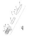
- FIG. 1is an exploded perspective view of a prior art reed relay configuration
- FIG. 2is perspective view a reed relay device in accordance with the present invention.
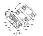
- FIG. 3is an exploded perspective view of the surface mount molded relay of the present invention.
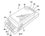
- FIG. 4is a perspective view of the surface mount molded relay package manufactured in accordance with the present invention.
- FIG. 5is a perspective view of the surface mount molded relay package of FIG. 4 prior to encapsulation
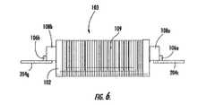
- FIG. 6is a right side elevational view of the reed relay affixed to a leadframe as shown in FIG. 5;
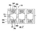
- FIG. 7is a plan view of an array of leadframes prior to installation of reed relays thereon;
- FIG. 8is a close-up top view of one of the leadframes of FIG. 7;
- FIG. 9is a graphical comparison of RF insertion loss of reed relay package with a printed circuit board of the prior art and a relay package manufactured in accordance with the present invention.
- FIG. 1a perspective view of a prior art reed switch configuration 1 0 is shown.
- a known reed switch 11includes a glass envelope 12 as well as two signal leads 14 emanating from opposing ends of the reed switch 11 and coil termination leads 15 .
- the construction of a reed switch 11is so well known in the art, the details thereof need not be discussed.
- a shield conductor 16commonly made of brass or copper, is provided in the form of a cylindrical sleeve which receives and houses the reed switch 11 .
- the reed switch 11 and shield 16are housed within the central bore 18 of a bobbin or spool 20 .
- About the bobbin 20is wound a conductive wire 22 .
- a co-axial arrangementis formed to protect the reed switch 11 device and to control the impedance of the environment and to improve the overall transmission of the signal.
- the reed switch 11 , shield conductor 16 and bobbin 20are shown in general as cylindrical in configuration.
- the reed switch 11is preferably of the normally open type but may also be of the normally closed type.
- the free ends of the coil of wire 22 , the shield 16 and signal terminals 14 of the reed switch 11are electrically interconnected to a circuit as desired.
- the respective components of the reed switch 11 configurationare interconnected to a circuit by another electrical interconnection (not shown).
- the electrical interconnection methods of the prior artintroduces a discontinuity of the desirable co-axial environment.
- the overall reed switch device 10must be designed to be easily accommodated within a user's circuit.
- a circuit used to operate at high frequencyis designed with a defined characteristic impedance environment.
- the goal of designing and manufacturing a reed device 10 to the specifications of a circuit customeris to match the desired impedance of the device 10 to the circuit environment as closely as possible. It is preferred that there is no discontinuity of impedance from the reed device 10 itself to a circuit board trace of the circuit that will receive the device 10 .
- the characteristic impedance, Z 1is generally a function of the outer diameter of the signal conductor 14 , the inner diameter of the shield 16 and the dielectric constant of the insulation (not shown) between the signal conductor 14 and the shield 16 .
- the present inventionincludes a reed switch 111 with a pair of signal terminals 106 a and 106 b emanating from opposing sides thereof.
- a glass envelope 126is provided with the contact tongues (not shown) therein. Details of the reed switch 111 is not discussed herein as it is well known in the prior art.
- the reed device 103is provided to include an outer bobbin 102 with coil 109 , with free ends 115 a and 115 b, wrapped around it for introducing the necessary magnetic field to actuate the reed switch 111 . Also emanating from the bobbin body 102 are ground shield tabs 108 a and 108 b in the form of arcuate semi-circles which are respectively electrically interconnected to opposing sides of the shield sleeve 110 . Each of the tabs 108 a and 108 b may also be in the form of a pair of tabs extending outwardly from sides of the ground shield sleeve 110 .
- Tab 108 ais positioned on one side of the bobbin body 102 and tab 108 b is positioned on the other side of the bobbin body 102 . Both tabs 108 a and 108 b are electrically interconnected to and emanating from the ends of the inner shield sleeve 110 . As shown in FIG. 3, an exploded perspective view the reed switch 111 of FIG. 2, the ground tabs 108 a and 108 b are, essentially, an extension from the shield sleeve 110 itself on opposing sides thereof whereby a pair of solderable surfaces 108 b and 108 d are provided on the lower edge of the tab 108 a and a pair of solderable surfaces 108 e and 108 f.
- a completed encapsulated reed switch package 200is shown in accordance with the present invention to include a main body portion 202 and a number of electrical contacts 204 a - h, which are preferably include solder balls 206 thereon which are affixed to conductors 204 a - h which are, in turn, connected to the various components of the reed switch package 200 .
- the construction of the conductors 204 a - h and solder balls 206 thereonwill be discussed in detail below.
- the reed switch package 200can be easily surface mounted to a circuit board for incorporation into a circuit (not shown).
- the surface mounting of reed switch device packages and electrical interconnection to a circuit on a circuit boardare so well known in the art that they need not be discussed in detail herein.
- FIGS. 5 - 8details of the construction of the reed switch package 200 of the present invention is shown.
- the reed switch package 200is shown prior to encapsulation to illustrate the construction and interconnection of the reed switch device 103 to a leadframe substrate 212 to provide a unique surface mountable reed switch device package 200 .
- the leadframe 212includes an array of sets of conductors 204 a - h for receiving a number of reed switch devices.
- an array of 10 leadframe unitsmay be employed for simultaneously manufacturing 10 reed switch device packages 200 .
- the first leadframe unitwill be discussed in detail.
- the leadframe 212includes an outer carrier frame 214 with a number of conductors 204 a - h emanating inwardly therefrom for electrical interconnection to various components of the reed switch device 103 .
- the conductors 204 a - hare employed to provide an interface of the reed switch device 103 to the circuit of the circuit board onto the which the package 200 is installed.
- a signal conductors 204 c and 204 care provided both sides of the reed switch device 103 to respectively interconnect with the signal terminals 106 a and 106 b. Also, on the front of the device 103 , ground conductors 204 b and 204 d are respectively electrically interconnect with the ground shield surfaces 108 c and 108 d. On the rear of the device, ground conductors 204 f and 204 h are respectively electrically interconnected with the ground shield surfaces 108 e and 108 f.
- FIG. 6further illustrates a right side elevational view of the construction of FIG. 5 where the signal terminals 106 a and 106 b are respectively electrically interconnected to their corresponding conductors 204 c and 204 g.
- the foregoing electrical interconnectionsare preferably made by soldering but could be accomplished by other methods known in the art, such as welding or thermal compression bonding.
- a leadframe structure of the present inventionwhich is optimized for use in an electromechanical switch package, is not found in the prior art.
- reed relays designed to transmit RF frequenciesneed special design features.
- One design difficulty with RF relaysis to transition from the internal circular coaxial structure of the reed switch and its shield, to the planar structure needed to affix the relay to an external circuit board.
- Prior art design approacheswas to use a printed circuit board with copper traces formed as striplines. It is well known in RF design that one method to transmit RF signals with minimized power loss is to provide a flat signal conductor flanked on either side by parallel grounded conductors which is an arrangement known as a coplanar waveguide.
- this impedanceis 50 ohms.
- the new leadframe structure 212achieves this desirable 50 ohm impedance by using some of the leadframe elements to form a tuned stripline.
- the leadframe 212is manufactured so that the elements connecting the reed switch terminals 106 a and 106 b and the internal RF ground shield 110 via contact surfaces 108 c - f to the exterior of the relay form a tuned transmission path with 50 ohm impedance.
- the dimensions and spacing of the elementsare adjusted to match the dielectric constant of the molding compound 217 , as seen in FIG. 4, used to encapsulate the reed switch device 103 .
- the conductors 204 a - hare conducive to maintaining the desired 50 ohm impedance.
- the exterior wasteis cropped away, leaving embedded contacts 204 a - h that allow the package 200 to be surface-mounted to the customer's circuit board.
- the attachmentis preferably made using solder balls 206 but may also be solder bumps, or other interconnection structures, such as land grid arrays (LGA), column grid arrays (CGA) or pin grid arrays (PGA) as well as solder paste dots, raised dimples, and the like.
- the present inventionachieves the desired 50 ohm impedance by optimizing the leadframe 212 for the high frequency environment.
- the use of a metal leadframe 212permits certain materials to be used as conductors 204 a - h and contacts 206 instead of the printable materials, such as copper, aluminum and tin which are commonly used in printed circuit boards.
- the leadframe 212is preferably formed from nickel-iron alloy, which can be later plated with other metals to improve the solderability or RF transmission characteristics. Copper may also be used.
- high conductivity silver platingcan be used to improve high frequency transmission, since GHz range signals travel mainly near the skin of a conductor.
- nickel-iron or other magnetically soft materialis particularly desirable for the base metal, since it improves the magnetic efficiency and hence reduces the power consumption of the relay.
- the use of a metal conductors rather than traces on the surface of a printed circuit boardprovides mechanical advantages as well.
- FIGS. 7 and 8, the mechanical advantages of the metal leadframe 212are shown more clearly.
- the use of a metal strip linesenables indents 216 to be formed in the interconnection end of the signal conductors 204 c and 204 g to form a seat to better receive the signal terminals of the reed switch.
- the indents 216are each approximately half as deep as the diameter of switch wire leads 106 a and 106 b, and serves as an alignment recess during relay assembly. It also improves RF transmission characteristics, since the high frequency signal travels in a straighter path through the relay. Discontinuities, caused by bends in the path which introduce impedance discontinuities that reduce RF transmission efficiency, are avoided in the package 200 of the present invention.
- each of the conductors 204 a - h of the leadframe 212also preferably have circular indents 218 formed on the free ends thereof, namely, in the region that is exposed after molding.
- Solder balls 206are located in these recesses 218 , improving their alignment by eliminating wander during attachment.
- FIG. 4shows the exposed positioning of the solder balls 206 in the recesses 218 on the free ends of the conductors 204 a - h in preparation for surface mount installation of the package 200 on a circuit board.
- the reed switch device 103is preferably partially assembled before encapsulation.
- the internal componentsare soldered to the leadframe 212 using a solder having a high enough melting point to withstand any subsequent manufacturing processes, such as fastening to a customer's circuit board.
- a solder having a high enough melting pointto withstand any subsequent manufacturing processes, such as fastening to a customer's circuit board.
- 100% tin or 95% tin+5% antimonyis used.
- welding or other metal joining processescan be used.
- the solder balls 206have been soldered into the circular recesses 218 in the conductors 204 a - h.
- the balls 206are preferably made from 10% tin+90% lead and have a melting point of 302 degrees C. With such a high melting point, they do not melt at the temperatures used for reflowing the package 200 onto a users circuit board. However, this does not preclude using other types of solder balls 206 , such as conventional eutectic solder consisting of 63% tin+37% lead. Nor does it preclude omitting the solder balls 206 altogether, and fastening the package 200 to a user's circuit board using solder paste or other conventional surface mounting techniques.
- FIG. 4shows the reed switch package 200 of the present invention after encapsulation.
- the reed switch device 103is preferably overmolded with typical encapsulation material 217 , such as plastic or epoxy material, while still connected to the frame.
- typical encapsulation material 217such as plastic or epoxy material
- the surplus leadframe 212is cropped away, and excess molding flash is removed by routing or sandblasting.
- the truncated leadframe elementsnamely conductors 204 a - h and solder balls 206 thereon, appear as bars embedded in the encapsulant 217 and are ready for surface mount interconnection to a circuit board.
- the overall height of the reed switch package 200is greatly reduced thus allowing for a low height installation of components on a circuit board to permit installation into smaller environments and to facilitate closer stacking of populated multiple circuit boards together.
- Test datashows that the package 200 of the present invention is an improvement over prior art packages.
- the chart of FIG. 11shows the RF insertion loss data for a prior art reed switch package made with an existing printed circuit board compared to the new reed switch package 200 with the metal leadframe 212 of the present invention.
- the vertical axisrepresents RF signal power loss in dB
- the horizontal axisrepresents frequency in GHz.
- the power loss as a function of frequencyis improved for the metal leadframe version up to a frequency of approximately 7 GHz, before both start to roll off to the minimum acceptable level of approximately 3 dB.
- the new reed switch package 200 of the present invention using a metal leadframe 212can provide RF transmission performance that is equivalent or better than the existing printed circuit board based designs of the prior art while still providing the advantages listed above.
- the present inventionprovides an improved reed switch device package 200 that includes a metal leadframe substrate 212 that is stronger and dimensionally more accurate than the existing printed board substrates used in prior art packages.
- the use of a metal leadframe 212 substrateminimizes breakage and distortion during manufacturing, and also ensures that the placement of solder balls 206 meets coplanarity requirements.
- the package 200 of the present inventionmore effectively provides electrical connection conductors 204 a - h between the exterior of the reed switch device 103 and the internal components by acting as a tuned waveguide with a nominal impedance of 50 ohms and minimum excursions from that impedance, thus minimizing RF power loss in a signal transmitted through the relay. Because the leadframe conductor elements 204 a - h are dimensionally more accurate than traces plated onto printed circuit boards used in the prior art, the impedance discontinuities are less than those created by a circuit board substrate.
- the half-etched switch lead receptacle seats 216generates a straighter path for signals transmitted through the signal terminals 106 a and 106 of the switch device 103 thereby reducing impedance discontinuities that can distort RF signals or absorb power.
- Such recessed seats 216cannot be formed on traces that have been printed onto a printed circuit board assembly.
- the recesses 218 for receiving the solder balls 206further improves alignment during installation.
- Eliminating a fibrous circuit board substrate of the prior artimproves the overall hermetic sealing of the reed switch device package 200 of the present invention. This reduces the probability of moisture ingress that can lower the device's insulation resistance.
- a soft magnetic materialsuch as Nickel/iron (NiFe) alloy for the leadframe substrate 212 improves the magnetic efficiency of the device because it acts as a magnetic antenna. This focuses the field lines generated by the relay coil 109 , allowing the reed switch device 103 to be closed with less electrical power than would be needed if copper leads were used. This means that either (a), lower power is needed to close the reed switch 111 or (b) a slightly stronger switch having higher reliability can be closed with the same power. Circuit board traces cannot be easily constructed from NiFe alloy. Even if fabrication method was developed, the limits of magnetic saturation would result in a conductor that was too thin to be useful for boosting magnetic efficiency.
- NiFeNickel/iron
- the package 200 of the present inventionreduces manufacturing costs and simplifies assembly and, as a result, achieves a more reliable product.
Landscapes
- Physics & Mathematics (AREA)
- Electromagnetism (AREA)
- Switches That Are Operated By Magnetic Or Electric Fields (AREA)
- Manufacture Of Switches (AREA)
- Encapsulation Of And Coatings For Semiconductor Or Solid State Devices (AREA)
- Auxiliary Devices For And Details Of Packaging Control (AREA)
- Mounting Components In General For Electric Apparatus (AREA)
- Injection Moulding Of Plastics Or The Like (AREA)
Abstract
Description
- This application claims priority from Provisional Patent Application Serial No. 60/362,856, filed Mar. 8, 2002.[0001]
- The present invention relates generally to switching devices. More specifically, the present invention relates to improved packaging and circuit integration for electromagnetic devices, such as reed switches and electromagnetic devices, such as reed relays, for switching high frequency signals. These relays are intended for applications in industries such as Automated Testing Equipment (ATE), where test signals having frequency ranges from DC to 12 GHz must be switched with minimum power loss and minimum pulse distortion.[0002]
- Electromagnetic relays have been known in the electronics industry for many years. Such electromagnetic relays include the reed relay which incorporates a reed switch. A reed switch is a magnetically activated device that typically includes two flat contact tongues which are merged in a hermetically sealed glass tube filled with a protective inert gas or vacuum. The switch is operated by an externally generated magnetic field, either from a coil or a permanent magnet. When the external magnetic field is enabled, the overlapping contact tongue ends attract each other and ultimately come into contact to close the switch. When the magnetic field is removed, the contact tongues demagnetize and spring back to return to their rest positions, thus opening the switch.[0003]
- Reed switches, actuated by a magnetic coil, are typically housed within a bobbin or spool-like member. A coil of wire is wrapped about the outside of the bobbin and connected to a source of electric current. The current flowing through the coil creates the desired magnetic field to actuate the reed switch within the bobbin housing. Some applications of reed devices require the switch to carry signals with frequencies in excess of 500 MHz. For these applications, a ground shield conductor, commonly made of copper or brass is disposed about the body of the reed switch. The ground shield conductor is commonly in a cylindrical configuration. The shield conductor resides between the reed switch and the bobbin housing to form a co-axial high frequency transmission system. This co-axial system includes the outer shield conductor and the switch lead signal conductor co-axially through the center of the reed switch. The ground shield conductor is employed to contain the signal through the switch conductor in order to maintain the desired impedance of the signal path.[0004]
- Currently available reed devices are then incorporated into a given circuit environment by users. For application at higher frequencies, a reed switch device must be ideally configured to match as closely as possible the desired impedance requirements of the circuit in which it is installed.[0005]
- Within a circuit environment, a co-axial arrangement is preferred throughout the entire environment to maintain circuit integrity and the desired matched impedance. As stated above, the body of a reed switch includes the necessary co-axial environment. In addition, the signal trace on the user's circuit board commonly includes a “wave guide” where two ground leads reside on opposing sides of the signal lead and in the same plane or a “strip line” where a ground plane resides below the plane of the signal conductor. These techniques properly employed provide a two-dimensional, controlled impedance environment which is acceptable for maintaining the desired impedance for proper circuit function.[0006]
- However, the reed switch device must be physically packaged and electrically interconnected to a circuit board carrying a given circuit configuration. It is common to terminate the shield and signal terminals to a lead frame architecture and enclose the entire assembly in a dielectric material like plastic for manufacturing and packaging ease. The external portion of the leads may be formed in a gull-wing or “J” shape for surface mount capability. The signal leads or terminals exit out of the reed switch body and into the air in order to make the electrical interconnection to the circuit board. This transition of the signal leads from plastic dielectric to air creates an undesirable discontinuity of the protective co-axial environment found within the body of the switch itself. Such discontinuity creates inaccuracy and uncertainty in the impedance of the reed switch device. As a result, circuit designers must compensate for this problem by specifically designing their circuits to accommodate and anticipate the inherent problems associated with the discontinuity of the protective co-axial environment and the degradation of the rated impedance of the reed switch device.[0007]
- For example, the circuit may be tuned to compensate for the discontinuity by adding parasitic inductance and capacitance. This method of discontinuity compensation is not preferred because it complicates and slows the design process and can degrade the integrity of the circuit. There is a demand to reduce the need to tune the circuit as described above. The prior art uses a structure of carefully designed vias, which are expensive and difficult to manufacture, to control the impedance from the relay to the board transition.[0008]
- There have been many attempts in the prior art to solve the aforementioned problems associated with the packaging and the incorporation of reed switch devices into a circuit. For example, prior art reed switch devices typically include a printed circuit board substrate onto which the reed switch itself is installed. Circuit board traces are deposited on the surface of the printed circuit board to provide a wave guide to extend the co-axial environment of the relay from the reed switch itself down to the main circuit board into which the device package is installed. However, there are problems associated with the use of a printed circuit board as a substrate within an overmolded device package as well as manufacturing limitations.[0009]
- Since it is commonly desired that the reed switch package be as small as possible, the use of a very thin printed circuit board is required. While a thin printed circuit board substrate has good RF transmission characteristics, it is less than ideal mechanically. The epoxy/fiberglass material of a typical printed circuit board is thin and fragile, and is subject to distortion or cracking under the heat and pressure stresses of the encapsulation process. Distortion of the leads can lead to misalignment of the solder balls when they are fastened to the product after molding. If the misalignment is severe, one or more relay balls can miss the solder pads on the user's circuit board when the relay is fastened, causing electrical discontinuities that require expensive rework.[0010]
- The substrate solder pads are also fragile and are, therefore, easily damaged when the relay solder balls are reflow soldered to the substrate. A further disadvantage of solder pads is that they are flat; because of this, the solder balls can wander on them during attachment, causing further misalignment. After the relay is molded, solder balls are fixed to pads provided on the exposed external portions of the substrate traces. The solder balls melt when the relay is applied to the user's circuit board, providing the electrical connections to the reed switch, coaxial shield and coil. Since the circuit board substrate has a fibrous edge profile that is exposed at the exterior of the relay, it also provides a potential path for ingress of moisture during circuit board cleaning processes. Water ingress is highly undesirable, since it can lower the relay's insulation resistance. Also, the printed circuit board is relatively expensive compared to the total component cost for the entire product. Therefore, it is desired for this part to be removed from the construction.[0011]
- In the prior art, there have been attempts to eliminate the use of printed circuit board substrates in electronic device packages. Many molded electronic packages use an internal metal leadframe skeleton to support internal components and transmit electrical signals in and out of the package. The leadframe supports the internal components during assembly, and is cut away after the product is molded leaving legs or pins that are used for external connections.[0012]
- A metal leadframe could provide such features to obviate the need for a printed circuit board provided that it does not degrade the quality of the signals being transmitted through the relay. However, leadframes are generally not optimized for very high frequency signal transmission. At frequencies of several GHz and beyond, signals must be carried on special structures such as tuned striplines or waveguides to minimize losses. Known leadframe structures are not capable for accommodating such high frequency signals. In particular, known leadframe structures are not capable of meeting industry requirements for relays used for testing high speed memory and other semiconductors which is a loss of no more than half power (−3 dB) for signals up to 5 GHz (5×10[0013]9Hz) which fall into the radio frequency (RF) band. The deficiencies in known leadframe capability will continue to be particularly inadequate in the future as the above requirement is likely to rise to 20 Ghz and beyond over the next few years.
- In view of the foregoing, there is a demand for a reed switch device that includes a controlled impedance environment through the entire body of the package to the interconnection to a circuit. There is a particular demand for a reed switch device to be compact and of a low profile for installation into small spaces and for circuit board stacking. There is further a demand for reed switch devices that are of a surface mount configuration to optimize the high frequency of the performance of the system. Further, there is a demand for a reed switch device that can reduce the need to tune a circuit to compensate for an uncontrolled impedance environment. There is a further need for a reed relay package that is low in cost yet still robust and rugged in construction with the ability to transmit high frequency signals through a closed relay with minimum power loss.[0014]
- The present invention preserves the advantages of prior art electromagnetic switch devices, such as reed relays. In addition, it provides new advantages not found in currently available switching devices and overcomes many disadvantages of such currently available devices.[0015]
- The invention is generally directed to the novel and unique reed switch device with particular application in effectively interconnecting a reed switch device to a circuit on a circuit board in a low profile configuration. The reed switch package of the present invention enables the efficient and effective interconnection to a circuit board while being in an inexpensive construction.[0016]
- The electromechanical device of the present invention mounts forms a low profile, board surface mountable reed relay. The reed device package includes a reed switch with two signal terminals emanating from opposing sides thereof. A leadframe is employed with signal conductors and ground conductors. The signal conductors are respectively attached to each of the signal terminals. A ground shield surrounds the body of the reed switch. The ground conductors are connected to the ground shield on a first side of the reed switch with the signal conductor on one side of the reed switch being positioned between the two ground conductors. Another pair of ground conductors are connected to the ground shield on the other side of the switch and are similarly positioned with the other signal conductor positioned therebetween. The reed switch device is overmolded with encapsulation material with the exception of the free ends of the signal and ground conductors which receive solder balls thereon for surface mount installation to a circuit board. After encapsulation, excess portions of the leadframe are trimmed away.[0017]
- It is therefore an object of the present invention to provide a compact, low profile reed switch package.[0018]
- It is an object of the present invention to provide a reed switch device with a controlled impedance environment throughout the entire package.[0019]
- It is a further object of the present invention to provide a reed switch package with an improved substrate that is stronger and dimensionally more accurate than the existing printed circuit board substrates.[0020]
- A further object of the present invention is provide a reed switch package that has a substrate that minimizes breakage and distortion during manufacturing.[0021]
- Another object of the present invention is to provide a reed switch package that is capable of efficiently conducting high frequency signals.[0022]
- It is a further object of the present invention to provide a reed switch package that is inexpensive to manufacture and more reliable to assemble.[0023]
- It is yet a further object of the present invention to provide a reed switch package that has solder ball placement that meet coplanarity installation requirements.[0024]
- Another object of the present invention is to provide a reed switch package that can be easily surface mounted to a main circuit board.[0025]
- It is yet another object of the invention to provide a reed switch package with a metal substrate that is optimized for high frequency signal transmission.[0026]
- The novel features which are characteristic of the present invention are set forth in the appended claims. However, the invention's preferred embodiments, together with further objects and attendant advantages, will be best understood by reference to the following detailed description taken in connection with the accompanying drawings in which:[0027]
- FIG. 1 is an exploded perspective view of a prior art reed relay configuration;[0028]
- FIG. 2 is perspective view a reed relay device in accordance with the present invention;[0029]
- FIG. 3 is an exploded perspective view of the surface mount molded relay of the present invention;[0030]
- FIG. 4 is a perspective view of the surface mount molded relay package manufactured in accordance with the present invention;[0031]
- FIG. 5 is a perspective view of the surface mount molded relay package of FIG. 4 prior to encapsulation;[0032]
- FIG. 6 is a right side elevational view of the reed relay affixed to a leadframe as shown in FIG. 5;[0033]
- FIG. 7 is a plan view of an array of leadframes prior to installation of reed relays thereon;[0034]
- FIG. 8 is a close-up top view of one of the leadframes of FIG. 7; and[0035]
- FIG. 9 is a graphical comparison of RF insertion loss of reed relay package with a printed circuit board of the prior art and a relay package manufactured in accordance with the present invention.[0036]
- Turning first to FIG. 1, a perspective view of a prior art[0037]
reed switch configuration 10 is shown. A knownreed switch 11 includes aglass envelope 12 as well as two signal leads14 emanating from opposing ends of thereed switch 11 and coil termination leads15. The construction of areed switch 11 is so well known in the art, the details thereof need not be discussed. Ashield conductor 16, commonly made of brass or copper, is provided in the form of a cylindrical sleeve which receives and houses thereed switch 11. Thereed switch 11 andshield 16 are housed within thecentral bore 18 of a bobbin orspool 20. About thebobbin 20 is wound aconductive wire 22. As a result, a co-axial arrangement is formed to protect thereed switch 11 device and to control the impedance of the environment and to improve the overall transmission of the signal. Thereed switch 11,shield conductor 16 andbobbin 20 are shown in general as cylindrical in configuration. - It should be understood that various other configurations, such as those oval in cross-section, may be employed and still be within the scope of the present invention. Also, the[0038]
reed switch 11 is preferably of the normally open type but may also be of the normally closed type. - As can be understood and known in the prior art, the free ends of the coil of[0039]
wire 22, theshield 16 andsignal terminals 14 of thereed switch 11 are electrically interconnected to a circuit as desired. The respective components of thereed switch 11 configuration are interconnected to a circuit by another electrical interconnection (not shown). The electrical interconnection methods of the prior art introduces a discontinuity of the desirable co-axial environment. - As described above, the overall[0040]
reed switch device 10 must be designed to be easily accommodated within a user's circuit. For example, a circuit used to operate at high frequency is designed with a defined characteristic impedance environment. The goal of designing and manufacturing areed device 10 to the specifications of a circuit customer is to match the desired impedance of thedevice 10 to the circuit environment as closely as possible. It is preferred that there is no discontinuity of impedance from thereed device 10 itself to a circuit board trace of the circuit that will receive thedevice 10. The characteristic impedance, Z1is generally a function of the outer diameter of thesignal conductor 14, the inner diameter of theshield 16 and the dielectric constant of the insulation (not shown) between thesignal conductor 14 and theshield 16. - Turning now to FIGS. 2 and 3, the[0041]
reed switch device 103 used in the package of the preferred embodiment of the present invention is shown. Referring to FIG. 2, the present invention includes areed switch 111 with a pair ofsignal terminals glass envelope 126 is provided with the contact tongues (not shown) therein. Details of thereed switch 111 is not discussed herein as it is well known in the prior art. - The[0042]
reed device 103 is provided to include anouter bobbin 102 withcoil 109, withfree ends reed switch 111. Also emanating from thebobbin body 102 areground shield tabs shield sleeve 110. Each of thetabs ground shield sleeve 110.Tab 108ais positioned on one side of thebobbin body 102 andtab 108bis positioned on the other side of thebobbin body 102. Bothtabs inner shield sleeve 110. As shown in FIG. 3, an exploded perspective view thereed switch 111 of FIG. 2, theground tabs shield sleeve 110 itself on opposing sides thereof whereby a pair ofsolderable surfaces tab 108aand a pair ofsolderable surfaces - Referring now to FIG. 4, a completed encapsulated[0043]
reed switch package 200 is shown in accordance with the present invention to include amain body portion 202 and a number of electrical contacts204a-h,which are preferably includesolder balls 206 thereon which are affixed to conductors204a-hwhich are, in turn, connected to the various components of thereed switch package 200. The construction of the conductors204a-handsolder balls 206 thereon will be discussed in detail below. In view of the construction shown in FIG. 4, thereed switch package 200 can be easily surface mounted to a circuit board for incorporation into a circuit (not shown). The surface mounting of reed switch device packages and electrical interconnection to a circuit on a circuit board are so well known in the art that they need not be discussed in detail herein. - In FIGS.[0044]5-8, details of the construction of the
reed switch package 200 of the present invention is shown. Turning to FIG. 5, thereed switch package 200 is shown prior to encapsulation to illustrate the construction and interconnection of thereed switch device 103 to aleadframe substrate 212 to provide a unique surface mountable reedswitch device package 200. To facilitate mass manufacture, theleadframe 212 includes an array of sets of conductors204a-hfor receiving a number of reed switch devices. For example, an array of10 leadframe units may be employed for simultaneously manufacturing10 reed switch device packages200. For ease of illustration, the first leadframe unit will be discussed in detail. - The[0045]
leadframe 212 includes anouter carrier frame 214 with a number of conductors204a-hemanating inwardly therefrom for electrical interconnection to various components of thereed switch device 103. The conductors204a-hare employed to provide an interface of thereed switch device 103 to the circuit of the circuit board onto the which thepackage 200 is installed. - More specifically, on each side of the[0046]
reed switch device 103, there four electrical interconnections that need to be made for proper operation of thereed switch device 103 within thepackage 200 and incorporation into a circuit. Asignal conductors reed switch device 103 to respectively interconnect with thesignal terminals device 103,ground conductors ground conductors wire coil 109 are respectively electrically interconnected withconductors signal terminals conductors - The use of a leadframe structure of the present invention, which is optimized for use in an electromechanical switch package, is not found in the prior art. In general, reed relays designed to transmit RF frequencies need special design features. One design difficulty with RF relays is to transition from the internal circular coaxial structure of the reed switch and its shield, to the planar structure needed to affix the relay to an external circuit board. Prior art design approaches was to use a printed circuit board with copper traces formed as striplines. It is well known in RF design that one method to transmit RF signals with minimized power loss is to provide a flat signal conductor flanked on either side by parallel grounded conductors which is an arrangement known as a coplanar waveguide. By adjusting the dimensions of the conductors, the spacing between them and the dielectric constant of the medium in which they sit, it is possible to tune the transmission of the three-conductor stripline combination to a specific characteristic impedance. Conventionally, this impedance is 50 ohms.[0047]
- The[0048]
new leadframe structure 212, as best seen in FIGS. 5, 7 and8, achieves this desirable 50 ohm impedance by using some of the leadframe elements to form a tuned stripline. Theleadframe 212 is manufactured so that the elements connecting thereed switch terminals RF ground shield 110 via contact surfaces108c-fto the exterior of the relay form a tuned transmission path with 50 ohm impedance. The dimensions and spacing of the elements are adjusted to match the dielectric constant of themolding compound 217, as seen in FIG. 4, used to encapsulate thereed switch device 103. For example, it has been found that placing the conductors204a-ha distance of 0.45 mm and 0.65 mm in width is conducive to maintaining the desired 50 ohm impedance. After thepackage 200 is molded, the exterior waste is cropped away, leaving embedded contacts204a-hthat allow thepackage 200 to be surface-mounted to the customer's circuit board. The attachment is preferably made usingsolder balls 206 but may also be solder bumps, or other interconnection structures, such as land grid arrays (LGA), column grid arrays (CGA) or pin grid arrays (PGA) as well as solder paste dots, raised dimples, and the like. - While the general use of leadframes to create packages are generally known in the art, the present invention achieves the desired 50 ohm impedance by optimizing the[0049]
leadframe 212 for the high frequency environment. Most importantly, the use of ametal leadframe 212 permits certain materials to be used as conductors204a-handcontacts 206 instead of the printable materials, such as copper, aluminum and tin which are commonly used in printed circuit boards. - In particular, the[0050]
leadframe 212 is preferably formed from nickel-iron alloy, which can be later plated with other metals to improve the solderability or RF transmission characteristics. Copper may also be used. For example, high conductivity silver plating can be used to improve high frequency transmission, since GHz range signals travel mainly near the skin of a conductor. Moreover, nickel-iron or other magnetically soft material is particularly desirable for the base metal, since it improves the magnetic efficiency and hence reduces the power consumption of the relay. The foregoing optimizations of conductors204a-hcannot be used with printed circuit board based package due to the limitations of the printable copper, aluminum and tin material employed. - Still further, the use of a metal conductors rather than traces on the surface of a printed circuit board provides mechanical advantages as well. Referring now to FIGS. 7 and 8, the mechanical advantages of the[0051]
metal leadframe 212 are shown more clearly. As seen in FIG. 8, the use of a metal strip lines enablesindents 216 to be formed in the interconnection end of thesignal conductors indents 216 are each approximately half as deep as the diameter of switch wire leads106aand106b,and serves as an alignment recess during relay assembly. It also improves RF transmission characteristics, since the high frequency signal travels in a straighter path through the relay. Discontinuities, caused by bends in the path which introduce impedance discontinuities that reduce RF transmission efficiency, are avoided in thepackage 200 of the present invention. - Still further, as seen in FIG. 8, each of the conductors[0052]204a-hof the
leadframe 212 also preferably havecircular indents 218 formed on the free ends thereof, namely, in the region that is exposed after molding.Solder balls 206, as seen in FIG. 4, are located in theserecesses 218, improving their alignment by eliminating wander during attachment. FIG. 4 shows the exposed positioning of thesolder balls 206 in therecesses 218 on the free ends of the conductors204a-hin preparation for surface mount installation of thepackage 200 on a circuit board. - In connection with the construction and assembly of the[0053]
package 200, thereed switch device 103 is preferably partially assembled before encapsulation. The internal components are soldered to theleadframe 212 using a solder having a high enough melting point to withstand any subsequent manufacturing processes, such as fastening to a customer's circuit board. Typically, 100% tin or 95% tin+5% antimony is used. However, welding or other metal joining processes can be used. - The[0054]
solder balls 206 have been soldered into thecircular recesses 218 in the conductors204a-h.Theballs 206 are preferably made from 10% tin+90% lead and have a melting point of 302 degrees C. With such a high melting point, they do not melt at the temperatures used for reflowing thepackage 200 onto a users circuit board. However, this does not preclude using other types ofsolder balls 206, such as conventional eutectic solder consisting of 63% tin+37% lead. Nor does it preclude omitting thesolder balls 206 altogether, and fastening thepackage 200 to a user's circuit board using solder paste or other conventional surface mounting techniques. - FIG. 4, as described above, shows the[0055]
reed switch package 200 of the present invention after encapsulation. Thereed switch device 103 is preferably overmolded withtypical encapsulation material 217, such as plastic or epoxy material, while still connected to the frame. Complete encapsulation provides an air-tight and/or liquid-tight seal thereby protecting the components therein. - After encapsulation is complete, the[0056]
surplus leadframe 212 is cropped away, and excess molding flash is removed by routing or sandblasting. As shown in FIG. 4, the truncated leadframe elements, namely conductors204a-handsolder balls 206 thereon, appear as bars embedded in theencapsulant 217 and are ready for surface mount interconnection to a circuit board. The overall height of thereed switch package 200 is greatly reduced thus allowing for a low height installation of components on a circuit board to permit installation into smaller environments and to facilitate closer stacking of populated multiple circuit boards together. - Test data shows that the[0057]
package 200 of the present invention is an improvement over prior art packages. The chart of FIG. 11 shows the RF insertion loss data for a prior art reed switch package made with an existing printed circuit board compared to the newreed switch package 200 with themetal leadframe 212 of the present invention. The vertical axis represents RF signal power loss in dB, and the horizontal axis represents frequency in GHz. The power loss as a function of frequency is improved for the metal leadframe version up to a frequency of approximately 7 GHz, before both start to roll off to the minimum acceptable level of approximately 3 dB. In view of the foregoing, the newreed switch package 200 of the present invention using ametal leadframe 212 can provide RF transmission performance that is equivalent or better than the existing printed circuit board based designs of the prior art while still providing the advantages listed above. - In view of the foregoing, the present invention provides an improved reed[0058]
switch device package 200 that includes ametal leadframe substrate 212 that is stronger and dimensionally more accurate than the existing printed board substrates used in prior art packages. The use of ametal leadframe 212 substrate minimizes breakage and distortion during manufacturing, and also ensures that the placement ofsolder balls 206 meets coplanarity requirements. - The[0059]
package 200 of the present invention more effectively provides electrical connection conductors204a-hbetween the exterior of thereed switch device 103 and the internal components by acting as a tuned waveguide with a nominal impedance of 50 ohms and minimum excursions from that impedance, thus minimizing RF power loss in a signal transmitted through the relay. Because the leadframe conductor elements204a-hare dimensionally more accurate than traces plated onto printed circuit boards used in the prior art, the impedance discontinuities are less than those created by a circuit board substrate. - The half-etched switch[0060]
lead receptacle seats 216 generates a straighter path for signals transmitted through thesignal terminals 106aand106 of theswitch device 103 thereby reducing impedance discontinuities that can distort RF signals or absorb power. Such recessedseats 216 cannot be formed on traces that have been printed onto a printed circuit board assembly. Therecesses 218 for receiving thesolder balls 206 further improves alignment during installation. - Eliminating a fibrous circuit board substrate of the prior art improves the overall hermetic sealing of the reed[0061]
switch device package 200 of the present invention. This reduces the probability of moisture ingress that can lower the device's insulation resistance. - Further, allowing the use of a soft magnetic material such as Nickel/iron (NiFe) alloy for the[0062]
leadframe substrate 212 improves the magnetic efficiency of the device because it acts as a magnetic antenna. This focuses the field lines generated by therelay coil 109, allowing thereed switch device 103 to be closed with less electrical power than would be needed if copper leads were used. This means that either (a), lower power is needed to close thereed switch 111 or (b) a slightly stronger switch having higher reliability can be closed with the same power. Circuit board traces cannot be easily constructed from NiFe alloy. Even if fabrication method was developed, the limits of magnetic saturation would result in a conductor that was too thin to be useful for boosting magnetic efficiency. - Overall, the[0063]
package 200 of the present invention reduces manufacturing costs and simplifies assembly and, as a result, achieves a more reliable product. - It would be appreciated by those skilled in the art that various changes and modifications can be made to the illustrated embodiments without departing from the spirit of the present invention. All such modifications and changes are intended to be covered by the appended claims.[0064]
Claims (47)
Priority Applications (1)
| Application Number | Priority Date | Filing Date | Title |
|---|---|---|---|
| US10/249,001US6683518B2 (en) | 2002-03-08 | 2003-03-07 | Surface mount molded relay package and method of manufacturing same |
Applications Claiming Priority (2)
| Application Number | Priority Date | Filing Date | Title |
|---|---|---|---|
| US36285602P | 2002-03-08 | 2002-03-08 | |
| US10/249,001US6683518B2 (en) | 2002-03-08 | 2003-03-07 | Surface mount molded relay package and method of manufacturing same |
Publications (2)
| Publication Number | Publication Date |
|---|---|
| US20030169138A1true US20030169138A1 (en) | 2003-09-11 |
| US6683518B2 US6683518B2 (en) | 2004-01-27 |
Family
ID=27805238
Family Applications (1)
| Application Number | Title | Priority Date | Filing Date |
|---|---|---|---|
| US10/249,001Expired - Fee RelatedUS6683518B2 (en) | 2002-03-08 | 2003-03-07 | Surface mount molded relay package and method of manufacturing same |
Country Status (9)
| Country | Link |
|---|---|
| US (1) | US6683518B2 (en) |
| EP (1) | EP1483769B1 (en) |
| AT (1) | ATE373869T1 (en) |
| AU (1) | AU2003230602A1 (en) |
| DE (1) | DE60316412T2 (en) |
| DK (1) | DK1483769T3 (en) |
| ES (1) | ES2294279T3 (en) |
| TW (1) | TWI226073B (en) |
| WO (1) | WO2003077269A2 (en) |
Cited By (8)
| Publication number | Priority date | Publication date | Assignee | Title |
|---|---|---|---|---|
| US20070090905A1 (en)* | 2004-05-19 | 2007-04-26 | Volvo Lastvagnar Ab | Magnetic switch arrangement and method for obtaining a differential magnetic switch |
| EP1670013A3 (en)* | 2004-12-09 | 2007-08-22 | EATON Corporation | Electrical switching apparatus including a housing and a trip circuit forming a composite structure |
| US20070279161A1 (en)* | 2006-05-30 | 2007-12-06 | Chen-Kai Lin | Method using a current to control a switch |
| FR2907962A1 (en)* | 2006-10-30 | 2008-05-02 | Valeo Securite Habitacle Sas | Switch module e.g. low current switch module, fabricating method for motor vehicle, involves encapsulating assembly including conductor track, relay, components and connectors, and cutting connector tracks to separate conducting circuits |
| WO2008055165A1 (en)* | 2006-10-31 | 2008-05-08 | Honeywell International Inc. | Integrated thermostat overmolded leadwire construction |
| US20140312997A1 (en)* | 2013-03-22 | 2014-10-23 | Pickering Electronics Limited | Encapsulated Reed Relay |
| WO2015135130A1 (en)* | 2014-03-11 | 2015-09-17 | 深圳市智优电池集成技术有限公司 | Reed switch relay |
| AT16658U1 (en)* | 2018-03-14 | 2020-04-15 | Tridonic Gmbh & Co Kg | Positioning and assembly aid for coils on printed circuit boards |
Families Citing this family (4)
| Publication number | Priority date | Publication date | Assignee | Title |
|---|---|---|---|---|
| JP2005129452A (en)* | 2003-10-27 | 2005-05-19 | Agilent Technol Inc | Reed relay with conductive bushing and offset current canceling method |
| US8581113B2 (en)* | 2007-12-19 | 2013-11-12 | Bridgewave Communications, Inc. | Low cost high frequency device package and methods |
| JP2011520219A (en) | 2008-04-15 | 2011-07-14 | コト テクノロジー,インコーポレーテッド | Improved Form C relay and package using the relay |
| US7920038B1 (en)* | 2008-05-20 | 2011-04-05 | Keithley Instruments, Inc. | Dual shielded relay |
Citations (50)
| Publication number | Priority date | Publication date | Assignee | Title |
|---|---|---|---|---|
| US3575678A (en)* | 1969-10-06 | 1971-04-20 | Grigsby Barton Inc | Reed switch assembly |
| US3939381A (en)* | 1974-03-22 | 1976-02-17 | Mcm Industries, Inc. | Universal burn-in fixture |
| US4947235A (en)* | 1989-02-21 | 1990-08-07 | Delco Electronics Corporation | Integrated circuit shield |
| US4975761A (en)* | 1989-09-05 | 1990-12-04 | Advanced Micro Devices, Inc. | High performance plastic encapsulated package for integrated circuit die |
| US5043534A (en)* | 1990-07-02 | 1991-08-27 | Olin Corporation | Metal electronic package having improved resistance to electromagnetic interference |
| US5175613A (en)* | 1991-01-18 | 1992-12-29 | Digital Equipment Corporation | Package for EMI, ESD, thermal, and mechanical shock protection of circuit chips |
| US5239198A (en)* | 1989-09-06 | 1993-08-24 | Motorola, Inc. | Overmolded semiconductor device having solder ball and edge lead connective structure |
| US5294826A (en)* | 1993-04-16 | 1994-03-15 | Northern Telecom Limited | Integrated circuit package and assembly thereof for thermal and EMI management |
| US5355016A (en)* | 1993-05-03 | 1994-10-11 | Motorola, Inc. | Shielded EPROM package |
| US5400949A (en)* | 1991-09-19 | 1995-03-28 | Nokia Mobile Phones Ltd. | Circuit board assembly |
| US5403782A (en)* | 1992-12-21 | 1995-04-04 | Sgs-Thomson Microelectronics, Inc. | Surface mountable integrated circuit package with integrated battery mount |
| US5422433A (en)* | 1993-11-15 | 1995-06-06 | Motorola, Inc. | Radio frequency isolation shield having reclosable opening |
| US5436203A (en)* | 1994-07-05 | 1995-07-25 | Motorola, Inc. | Shielded liquid encapsulated semiconductor device and method for making the same |
| US5459287A (en)* | 1994-05-18 | 1995-10-17 | Dell Usa, L.P. | Socketed printed circuit board BGA connection apparatus and associated methods |
| US5483423A (en)* | 1993-11-16 | 1996-01-09 | Digital Equipment Corporation | EMI shielding for components |
| US5485037A (en)* | 1993-04-12 | 1996-01-16 | Amkor Electronics, Inc. | Semiconductor device having a thermal dissipator and electromagnetic shielding |
| US5486720A (en)* | 1994-05-26 | 1996-01-23 | Analog Devices, Inc. | EMF shielding of an integrated circuit package |
| US5525834A (en)* | 1994-10-17 | 1996-06-11 | W. L. Gore & Associates, Inc. | Integrated circuit package |
| US5530202A (en)* | 1995-01-09 | 1996-06-25 | At&T Corp. | Metallic RF or thermal shield for automatic vacuum placement |
| US5535101A (en)* | 1992-11-03 | 1996-07-09 | Motorola, Inc. | Leadless integrated circuit package |
| US5541450A (en)* | 1994-11-02 | 1996-07-30 | Motorola, Inc. | Low-profile ball-grid array semiconductor package |
| US5543663A (en)* | 1993-12-27 | 1996-08-06 | Kabushiki Kaisha Toshiba | Semiconductor device and BGA package |
| US5557142A (en)* | 1991-02-04 | 1996-09-17 | Motorola, Inc. | Shielded semiconductor device package |
| US5559306A (en)* | 1994-05-17 | 1996-09-24 | Olin Corporation | Electronic package with improved electrical performance |
| US5561265A (en)* | 1993-03-24 | 1996-10-01 | Northern Telecom Limited | Integrated circuit packaging |
| US5566055A (en)* | 1995-03-03 | 1996-10-15 | Parker-Hannifin Corporation | Shieled enclosure for electronics |
| US5574314A (en)* | 1994-07-28 | 1996-11-12 | Mitsubishi Denki Kabushiki Kaisha | Packaged semiconductor device including shielded inner walls |
| US5583378A (en)* | 1994-05-16 | 1996-12-10 | Amkor Electronics, Inc. | Ball grid array integrated circuit package with thermal conductor |
| US5629835A (en)* | 1994-07-19 | 1997-05-13 | Olin Corporation | Metal ball grid array package with improved thermal conductivity |
| US5633786A (en)* | 1995-08-21 | 1997-05-27 | Motorola | Shield assembly and method of shielding suitable for use in a communication device |
| US5640048A (en)* | 1994-07-11 | 1997-06-17 | Sun Microsystems, Inc. | Ball grid array package for a integrated circuit |
| US5650659A (en)* | 1995-08-04 | 1997-07-22 | National Semiconductor Corporation | Semiconductor component package assembly including an integral RF/EMI shield |
| US5666272A (en)* | 1994-11-29 | 1997-09-09 | Sgs-Thomson Microelectronics, Inc. | Detachable module/ball grid array package |
| US5668406A (en)* | 1994-05-31 | 1997-09-16 | Nec Corporation | Semiconductor device having shielding structure made of electrically conductive paste |
| US5684441A (en)* | 1996-02-29 | 1997-11-04 | Graeber; Roger R. | Reverse power protection circuit and relay |
| US5694300A (en)* | 1996-04-01 | 1997-12-02 | Northrop Grumman Corporation | Electromagnetically channelized microwave integrated circuit |
| US5701032A (en)* | 1994-10-17 | 1997-12-23 | W. L. Gore & Associates, Inc. | Integrated circuit package |
| US5708567A (en)* | 1995-11-15 | 1998-01-13 | Anam Industrial Co., Ltd. | Ball grid array semiconductor package with ring-type heat sink |
| US5777382A (en)* | 1995-12-19 | 1998-07-07 | Texas Instruments Incorporated | Plastic packaging for a surface mounted integrated circuit |
| US5789068A (en)* | 1995-06-29 | 1998-08-04 | Fry's Metals, Inc. | Preformed solder parts coated with parylene in a thickness effective to exhibit predetermined interference colors |
| US5789815A (en)* | 1996-04-23 | 1998-08-04 | Motorola, Inc. | Three dimensional semiconductor package having flexible appendages |
| US5796170A (en)* | 1996-02-15 | 1998-08-18 | Northern Telecom Limited | Ball grid array (BGA) integrated circuit packages |
| US5798567A (en)* | 1997-08-21 | 1998-08-25 | Hewlett-Packard Company | Ball grid array integrated circuit package which employs a flip chip integrated circuit and decoupling capacitors |
| US5819398A (en)* | 1995-07-31 | 1998-10-13 | Sgs-Thomson Microelectronics, Ltd. | Method of manufacturing a ball grid array package |
| US5831832A (en)* | 1997-08-11 | 1998-11-03 | Motorola, Inc. | Molded plastic ball grid array package |
| US5838551A (en)* | 1996-08-01 | 1998-11-17 | Northern Telecom Limited | Electronic package carrying an electronic component and assembly of mother board and electronic package |
| US5854512A (en)* | 1996-09-20 | 1998-12-29 | Vlsi Technology, Inc. | High density leaded ball-grid array package |
| US6025768A (en)* | 1999-03-12 | 2000-02-15 | Kearny-National, Inc. | Electromechanical switching device package with controlled impedance environment |
| US6052045A (en)* | 1999-03-12 | 2000-04-18 | Kearney-National, Inc. | Electromechanical switching device package with controlled impedance environment |
| US6294971B1 (en)* | 2000-07-21 | 2001-09-25 | Kearney-National Inc. | Inverted board mounted electromechanical device |
Family Cites Families (2)
| Publication number | Priority date | Publication date | Assignee | Title |
|---|---|---|---|---|
| US6008708A (en)* | 1996-07-16 | 1999-12-28 | Fujitsu Takamisawa Component Limited | Reed relay and method for fabrication thereof |
| JPH11204010A (en)* | 1998-01-08 | 1999-07-30 | Fujitsu Takamisawa Component Ltd | Reed relay and manufacture thereof |
- 2003
- 2003-03-06EPEP03723687Apatent/EP1483769B1/ennot_activeExpired - Lifetime
- 2003-03-06DKDK03723687Tpatent/DK1483769T3/enactive
- 2003-03-06ESES03723687Tpatent/ES2294279T3/ennot_activeExpired - Lifetime
- 2003-03-06DEDE60316412Tpatent/DE60316412T2/ennot_activeExpired - Fee Related
- 2003-03-06WOPCT/US2003/006945patent/WO2003077269A2/enactiveIP Right Grant
- 2003-03-06AUAU2003230602Apatent/AU2003230602A1/ennot_activeAbandoned
- 2003-03-06ATAT03723687Tpatent/ATE373869T1/ennot_activeIP Right Cessation
- 2003-03-07TWTW092104916Apatent/TWI226073B/ennot_activeIP Right Cessation
- 2003-03-07USUS10/249,001patent/US6683518B2/ennot_activeExpired - Fee Related
Patent Citations (50)
| Publication number | Priority date | Publication date | Assignee | Title |
|---|---|---|---|---|
| US3575678A (en)* | 1969-10-06 | 1971-04-20 | Grigsby Barton Inc | Reed switch assembly |
| US3939381A (en)* | 1974-03-22 | 1976-02-17 | Mcm Industries, Inc. | Universal burn-in fixture |
| US4947235A (en)* | 1989-02-21 | 1990-08-07 | Delco Electronics Corporation | Integrated circuit shield |
| US4975761A (en)* | 1989-09-05 | 1990-12-04 | Advanced Micro Devices, Inc. | High performance plastic encapsulated package for integrated circuit die |
| US5239198A (en)* | 1989-09-06 | 1993-08-24 | Motorola, Inc. | Overmolded semiconductor device having solder ball and edge lead connective structure |
| US5043534A (en)* | 1990-07-02 | 1991-08-27 | Olin Corporation | Metal electronic package having improved resistance to electromagnetic interference |
| US5175613A (en)* | 1991-01-18 | 1992-12-29 | Digital Equipment Corporation | Package for EMI, ESD, thermal, and mechanical shock protection of circuit chips |
| US5557142A (en)* | 1991-02-04 | 1996-09-17 | Motorola, Inc. | Shielded semiconductor device package |
| US5400949A (en)* | 1991-09-19 | 1995-03-28 | Nokia Mobile Phones Ltd. | Circuit board assembly |
| US5535101A (en)* | 1992-11-03 | 1996-07-09 | Motorola, Inc. | Leadless integrated circuit package |
| US5403782A (en)* | 1992-12-21 | 1995-04-04 | Sgs-Thomson Microelectronics, Inc. | Surface mountable integrated circuit package with integrated battery mount |
| US5561265A (en)* | 1993-03-24 | 1996-10-01 | Northern Telecom Limited | Integrated circuit packaging |
| US5485037A (en)* | 1993-04-12 | 1996-01-16 | Amkor Electronics, Inc. | Semiconductor device having a thermal dissipator and electromagnetic shielding |
| US5294826A (en)* | 1993-04-16 | 1994-03-15 | Northern Telecom Limited | Integrated circuit package and assembly thereof for thermal and EMI management |
| US5355016A (en)* | 1993-05-03 | 1994-10-11 | Motorola, Inc. | Shielded EPROM package |
| US5422433A (en)* | 1993-11-15 | 1995-06-06 | Motorola, Inc. | Radio frequency isolation shield having reclosable opening |
| US5483423A (en)* | 1993-11-16 | 1996-01-09 | Digital Equipment Corporation | EMI shielding for components |
| US5543663A (en)* | 1993-12-27 | 1996-08-06 | Kabushiki Kaisha Toshiba | Semiconductor device and BGA package |
| US5583378A (en)* | 1994-05-16 | 1996-12-10 | Amkor Electronics, Inc. | Ball grid array integrated circuit package with thermal conductor |
| US5559306A (en)* | 1994-05-17 | 1996-09-24 | Olin Corporation | Electronic package with improved electrical performance |
| US5459287A (en)* | 1994-05-18 | 1995-10-17 | Dell Usa, L.P. | Socketed printed circuit board BGA connection apparatus and associated methods |
| US5486720A (en)* | 1994-05-26 | 1996-01-23 | Analog Devices, Inc. | EMF shielding of an integrated circuit package |
| US5668406A (en)* | 1994-05-31 | 1997-09-16 | Nec Corporation | Semiconductor device having shielding structure made of electrically conductive paste |
| US5436203A (en)* | 1994-07-05 | 1995-07-25 | Motorola, Inc. | Shielded liquid encapsulated semiconductor device and method for making the same |
| US5640048A (en)* | 1994-07-11 | 1997-06-17 | Sun Microsystems, Inc. | Ball grid array package for a integrated circuit |
| US5629835A (en)* | 1994-07-19 | 1997-05-13 | Olin Corporation | Metal ball grid array package with improved thermal conductivity |
| US5574314A (en)* | 1994-07-28 | 1996-11-12 | Mitsubishi Denki Kabushiki Kaisha | Packaged semiconductor device including shielded inner walls |
| US5701032A (en)* | 1994-10-17 | 1997-12-23 | W. L. Gore & Associates, Inc. | Integrated circuit package |
| US5525834A (en)* | 1994-10-17 | 1996-06-11 | W. L. Gore & Associates, Inc. | Integrated circuit package |
| US5541450A (en)* | 1994-11-02 | 1996-07-30 | Motorola, Inc. | Low-profile ball-grid array semiconductor package |
| US5666272A (en)* | 1994-11-29 | 1997-09-09 | Sgs-Thomson Microelectronics, Inc. | Detachable module/ball grid array package |
| US5530202A (en)* | 1995-01-09 | 1996-06-25 | At&T Corp. | Metallic RF or thermal shield for automatic vacuum placement |
| US5566055A (en)* | 1995-03-03 | 1996-10-15 | Parker-Hannifin Corporation | Shieled enclosure for electronics |
| US5789068A (en)* | 1995-06-29 | 1998-08-04 | Fry's Metals, Inc. | Preformed solder parts coated with parylene in a thickness effective to exhibit predetermined interference colors |
| US5819398A (en)* | 1995-07-31 | 1998-10-13 | Sgs-Thomson Microelectronics, Ltd. | Method of manufacturing a ball grid array package |
| US5650659A (en)* | 1995-08-04 | 1997-07-22 | National Semiconductor Corporation | Semiconductor component package assembly including an integral RF/EMI shield |
| US5633786A (en)* | 1995-08-21 | 1997-05-27 | Motorola | Shield assembly and method of shielding suitable for use in a communication device |
| US5708567A (en)* | 1995-11-15 | 1998-01-13 | Anam Industrial Co., Ltd. | Ball grid array semiconductor package with ring-type heat sink |
| US5777382A (en)* | 1995-12-19 | 1998-07-07 | Texas Instruments Incorporated | Plastic packaging for a surface mounted integrated circuit |
| US5796170A (en)* | 1996-02-15 | 1998-08-18 | Northern Telecom Limited | Ball grid array (BGA) integrated circuit packages |
| US5684441A (en)* | 1996-02-29 | 1997-11-04 | Graeber; Roger R. | Reverse power protection circuit and relay |
| US5694300A (en)* | 1996-04-01 | 1997-12-02 | Northrop Grumman Corporation | Electromagnetically channelized microwave integrated circuit |
| US5789815A (en)* | 1996-04-23 | 1998-08-04 | Motorola, Inc. | Three dimensional semiconductor package having flexible appendages |
| US5838551A (en)* | 1996-08-01 | 1998-11-17 | Northern Telecom Limited | Electronic package carrying an electronic component and assembly of mother board and electronic package |
| US5854512A (en)* | 1996-09-20 | 1998-12-29 | Vlsi Technology, Inc. | High density leaded ball-grid array package |
| US5831832A (en)* | 1997-08-11 | 1998-11-03 | Motorola, Inc. | Molded plastic ball grid array package |
| US5798567A (en)* | 1997-08-21 | 1998-08-25 | Hewlett-Packard Company | Ball grid array integrated circuit package which employs a flip chip integrated circuit and decoupling capacitors |
| US6025768A (en)* | 1999-03-12 | 2000-02-15 | Kearny-National, Inc. | Electromechanical switching device package with controlled impedance environment |
| US6052045A (en)* | 1999-03-12 | 2000-04-18 | Kearney-National, Inc. | Electromechanical switching device package with controlled impedance environment |
| US6294971B1 (en)* | 2000-07-21 | 2001-09-25 | Kearney-National Inc. | Inverted board mounted electromechanical device |
Cited By (17)
| Publication number | Priority date | Publication date | Assignee | Title |
|---|---|---|---|---|
| US7508288B2 (en)* | 2004-05-19 | 2009-03-24 | Volvo Lastvagnar Ab | Magnetic switch arrangement |
| US20070109084A1 (en)* | 2004-05-19 | 2007-05-17 | Van Glabeke Pierre | Magnetic switch arrangement |
| US20070090905A1 (en)* | 2004-05-19 | 2007-04-26 | Volvo Lastvagnar Ab | Magnetic switch arrangement and method for obtaining a differential magnetic switch |
| EP1670013A3 (en)* | 2004-12-09 | 2007-08-22 | EATON Corporation | Electrical switching apparatus including a housing and a trip circuit forming a composite structure |
| US20070279161A1 (en)* | 2006-05-30 | 2007-12-06 | Chen-Kai Lin | Method using a current to control a switch |
| FR2907962A1 (en)* | 2006-10-30 | 2008-05-02 | Valeo Securite Habitacle Sas | Switch module e.g. low current switch module, fabricating method for motor vehicle, involves encapsulating assembly including conductor track, relay, components and connectors, and cutting connector tracks to separate conducting circuits |
| WO2008052891A1 (en)* | 2006-10-30 | 2008-05-08 | Valeo Securite Habitacle | Method for production of a low current switch module and device obtained by said method |
| US20100214045A1 (en)* | 2006-10-30 | 2010-08-26 | Valeo Securite Habitacle | Method for production of a low current switch module and device obtained by said method |
| US8122592B2 (en) | 2006-10-30 | 2012-02-28 | Valeo Securite Habitacle | Method for producing a low-current switch module comprising electrical components |
| US20080148843A1 (en)* | 2006-10-31 | 2008-06-26 | Honeywell International Inc. | Integrated thermostat overmolded leadwire construction |
| WO2008055165A1 (en)* | 2006-10-31 | 2008-05-08 | Honeywell International Inc. | Integrated thermostat overmolded leadwire construction |
| US20140312997A1 (en)* | 2013-03-22 | 2014-10-23 | Pickering Electronics Limited | Encapsulated Reed Relay |
| GB2514247A (en)* | 2013-03-22 | 2014-11-19 | Pickering Electronics Ltd | Encapsulated reed relay |
| WO2015135130A1 (en)* | 2014-03-11 | 2015-09-17 | 深圳市智优电池集成技术有限公司 | Reed switch relay |
| CN106104739A (en)* | 2014-03-11 | 2016-11-09 | 深圳市智优电池集成技术有限公司 | A kind of reed switch relay |
| US10026575B2 (en) | 2014-03-11 | 2018-07-17 | Shenzhen Zhiyou Battery Integration Technology Co., Ltd | Reed relay |
| AT16658U1 (en)* | 2018-03-14 | 2020-04-15 | Tridonic Gmbh & Co Kg | Positioning and assembly aid for coils on printed circuit boards |
Also Published As
| Publication number | Publication date |
|---|---|
| EP1483769A4 (en) | 2005-10-26 |
| AU2003230602A1 (en) | 2003-09-22 |
| WO2003077269A2 (en) | 2003-09-18 |
| EP1483769A2 (en) | 2004-12-08 |
| EP1483769B1 (en) | 2007-09-19 |
| ATE373869T1 (en) | 2007-10-15 |
| ES2294279T3 (en) | 2008-04-01 |
| TWI226073B (en) | 2005-01-01 |
| WO2003077269A3 (en) | 2003-12-18 |
| DE60316412T2 (en) | 2008-11-20 |
| TW200402076A (en) | 2004-02-01 |
| AU2003230602A8 (en) | 2003-09-22 |
| DE60316412D1 (en) | 2007-10-31 |
| DK1483769T3 (en) | 2008-01-28 |
| US6683518B2 (en) | 2004-01-27 |
Similar Documents
| Publication | Publication Date | Title |
|---|---|---|
| US6683518B2 (en) | Surface mount molded relay package and method of manufacturing same | |
| US5352925A (en) | Semiconductor device with electromagnetic shield | |
| US6603193B2 (en) | Semiconductor package | |
| US5379185A (en) | Leadless surface mountable assembly | |
| EP1037236B1 (en) | Electromechanical switching device package with controlled impedance environment | |
| EP1269505B1 (en) | Inverted board mounted electromechanical device | |
| US8063725B2 (en) | Form C relay and package using same | |
| US6052045A (en) | Electromechanical switching device package with controlled impedance environment | |
| US6847115B2 (en) | Packaged semiconductor device for radio frequency shielding | |
| US4644096A (en) | Surface mounting package | |
| USRE38381E1 (en) | Inverted board mounted electromechanical device | |
| US6954126B2 (en) | Lead-less surface mount reed relay | |
| KR19990001809A (en) | Irreversible element and manufacturing method |
Legal Events
| Date | Code | Title | Description |
|---|---|---|---|
| AS | Assignment | Owner name:KEARNEY-NATIONAL, INC., A DELAWARE CORPORATION, NE Free format text:ASSIGNMENT OF ASSIGNORS INTEREST;ASSIGNOR:MOTTA, JAMES J.;REEL/FRAME:013576/0785 Effective date:20030324 | |
| AS | Assignment | Owner name:BANK OF AMERICA, N.A., AS ADMINISTRATIVE AGENT, NO Free format text:NOTICE OF GRANT OF SECURITY INTEREST;ASSIGNOR:KEARNEY-NATIONAL, INC.;REEL/FRAME:014734/0820 Effective date:20040526 | |
| FPAY | Fee payment | Year of fee payment:4 | |
| AS | Assignment | Owner name:COTO TECHNOLOGY, INC., RHODE ISLAND Free format text:ASSIGNMENT OF ASSIGNORS INTEREST;ASSIGNOR:KEARNEY-NATIONAL INC.;REEL/FRAME:019881/0483 Effective date:20070623 | |
| AS | Assignment | Owner name:BANK OF AMERICA, N.A., AS ADMINISTRATIVE AGENT, NO Free format text:NOTICE OF GRANT OF SECURITY INTEREST;ASSIGNOR:COTO TECHNOLOGY, INC.;REEL/FRAME:020092/0304 Effective date:20040526 | |
| AS | Assignment | Owner name:KEARNEY-NATIONAL, INC., NEW YORK Free format text:TERMINATION OF SECURITY INTEREST IN PATENTS;ASSIGNOR:BANK OF AMERICA, N.A., AS ADMINISTRATIVE AGENT;REEL/FRAME:026583/0318 Effective date:20110712 Owner name:COTO TECHNOLOGY, INC., RHODE ISLAND Free format text:TERMINATION OF SECURITY INTEREST IN PATENTS;ASSIGNOR:BANK OF AMERICA, N.A., AS ADMINISTRATIVE AGENT;REEL/FRAME:026583/0060 Effective date:20110712 | |
| REMI | Maintenance fee reminder mailed | ||
| LAPS | Lapse for failure to pay maintenance fees | ||
| STCH | Information on status: patent discontinuation | Free format text:PATENT EXPIRED DUE TO NONPAYMENT OF MAINTENANCE FEES UNDER 37 CFR 1.362 | |
| FP | Lapsed due to failure to pay maintenance fee | Effective date:20120127 |