US20030168725A1 - Methods of making microelectronic assemblies including folded substrates - Google Patents
Methods of making microelectronic assemblies including folded substratesDownload PDFInfo
- Publication number
- US20030168725A1 US20030168725A1US10/281,550US28155002AUS2003168725A1US 20030168725 A1US20030168725 A1US 20030168725A1US 28155002 AUS28155002 AUS 28155002AUS 2003168725 A1US2003168725 A1US 2003168725A1
- Authority
- US
- United States
- Prior art keywords
- subassembly
- assembly
- substrate
- contacts
- subassemblies
- Prior art date
- Legal status (The legal status is an assumption and is not a legal conclusion. Google has not performed a legal analysis and makes no representation as to the accuracy of the status listed.)
- Granted
Links
Images


Classifications
- H—ELECTRICITY
- H05—ELECTRIC TECHNIQUES NOT OTHERWISE PROVIDED FOR
- H05K—PRINTED CIRCUITS; CASINGS OR CONSTRUCTIONAL DETAILS OF ELECTRIC APPARATUS; MANUFACTURE OF ASSEMBLAGES OF ELECTRICAL COMPONENTS
- H05K1/00—Printed circuits
- H05K1/18—Printed circuits structurally associated with non-printed electric components
- H05K1/189—Printed circuits structurally associated with non-printed electric components characterised by the use of a flexible or folded printed circuit
- H—ELECTRICITY
- H01—ELECTRIC ELEMENTS
- H01L—SEMICONDUCTOR DEVICES NOT COVERED BY CLASS H10
- H01L23/00—Details of semiconductor or other solid state devices
- H01L23/52—Arrangements for conducting electric current within the device in operation from one component to another, i.e. interconnections, e.g. wires, lead frames
- H01L23/538—Arrangements for conducting electric current within the device in operation from one component to another, i.e. interconnections, e.g. wires, lead frames the interconnection structure between a plurality of semiconductor chips being formed on, or in, insulating substrates
- H01L23/5387—Flexible insulating substrates
- H—ELECTRICITY
- H01—ELECTRIC ELEMENTS
- H01L—SEMICONDUCTOR DEVICES NOT COVERED BY CLASS H10
- H01L25/00—Assemblies consisting of a plurality of semiconductor or other solid state devices
- H01L25/03—Assemblies consisting of a plurality of semiconductor or other solid state devices all the devices being of a type provided for in a single subclass of subclasses H10B, H10D, H10F, H10H, H10K or H10N, e.g. assemblies of rectifier diodes
- H01L25/04—Assemblies consisting of a plurality of semiconductor or other solid state devices all the devices being of a type provided for in a single subclass of subclasses H10B, H10D, H10F, H10H, H10K or H10N, e.g. assemblies of rectifier diodes the devices not having separate containers
- H01L25/065—Assemblies consisting of a plurality of semiconductor or other solid state devices all the devices being of a type provided for in a single subclass of subclasses H10B, H10D, H10F, H10H, H10K or H10N, e.g. assemblies of rectifier diodes the devices not having separate containers the devices being of a type provided for in group H10D89/00
- H01L25/0657—Stacked arrangements of devices
- H—ELECTRICITY
- H01—ELECTRIC ELEMENTS
- H01L—SEMICONDUCTOR DEVICES NOT COVERED BY CLASS H10
- H01L2224/00—Indexing scheme for arrangements for connecting or disconnecting semiconductor or solid-state bodies and methods related thereto as covered by H01L24/00
- H01L2224/01—Means for bonding being attached to, or being formed on, the surface to be connected, e.g. chip-to-package, die-attach, "first-level" interconnects; Manufacturing methods related thereto
- H01L2224/02—Bonding areas; Manufacturing methods related thereto
- H01L2224/04—Structure, shape, material or disposition of the bonding areas prior to the connecting process
- H01L2224/05—Structure, shape, material or disposition of the bonding areas prior to the connecting process of an individual bonding area
- H01L2224/0554—External layer
- H01L2224/0556—Disposition
- H01L2224/05568—Disposition the whole external layer protruding from the surface
- H—ELECTRICITY
- H01—ELECTRIC ELEMENTS
- H01L—SEMICONDUCTOR DEVICES NOT COVERED BY CLASS H10
- H01L2224/00—Indexing scheme for arrangements for connecting or disconnecting semiconductor or solid-state bodies and methods related thereto as covered by H01L24/00
- H01L2224/01—Means for bonding being attached to, or being formed on, the surface to be connected, e.g. chip-to-package, die-attach, "first-level" interconnects; Manufacturing methods related thereto
- H01L2224/02—Bonding areas; Manufacturing methods related thereto
- H01L2224/04—Structure, shape, material or disposition of the bonding areas prior to the connecting process
- H01L2224/05—Structure, shape, material or disposition of the bonding areas prior to the connecting process of an individual bonding area
- H01L2224/0554—External layer
- H01L2224/05573—Single external layer
- H—ELECTRICITY
- H01—ELECTRIC ELEMENTS
- H01L—SEMICONDUCTOR DEVICES NOT COVERED BY CLASS H10
- H01L2224/00—Indexing scheme for arrangements for connecting or disconnecting semiconductor or solid-state bodies and methods related thereto as covered by H01L24/00
- H01L2224/01—Means for bonding being attached to, or being formed on, the surface to be connected, e.g. chip-to-package, die-attach, "first-level" interconnects; Manufacturing methods related thereto
- H01L2224/10—Bump connectors; Manufacturing methods related thereto
- H01L2224/15—Structure, shape, material or disposition of the bump connectors after the connecting process
- H01L2224/16—Structure, shape, material or disposition of the bump connectors after the connecting process of an individual bump connector
- H—ELECTRICITY
- H01—ELECTRIC ELEMENTS
- H01L—SEMICONDUCTOR DEVICES NOT COVERED BY CLASS H10
- H01L2225/00—Details relating to assemblies covered by the group H01L25/00 but not provided for in its subgroups
- H01L2225/03—All the devices being of a type provided for in the same main group of the same subclass of class H10, e.g. assemblies of rectifier diodes
- H01L2225/04—All the devices being of a type provided for in the same main group of the same subclass of class H10, e.g. assemblies of rectifier diodes the devices not having separate containers
- H01L2225/065—All the devices being of a type provided for in the same main group of the same subclass of class H10
- H01L2225/06503—Stacked arrangements of devices
- H01L2225/06517—Bump or bump-like direct electrical connections from device to substrate
- H—ELECTRICITY
- H01—ELECTRIC ELEMENTS
- H01L—SEMICONDUCTOR DEVICES NOT COVERED BY CLASS H10
- H01L2225/00—Details relating to assemblies covered by the group H01L25/00 but not provided for in its subgroups
- H01L2225/03—All the devices being of a type provided for in the same main group of the same subclass of class H10, e.g. assemblies of rectifier diodes
- H01L2225/04—All the devices being of a type provided for in the same main group of the same subclass of class H10, e.g. assemblies of rectifier diodes the devices not having separate containers
- H01L2225/065—All the devices being of a type provided for in the same main group of the same subclass of class H10
- H01L2225/06503—Stacked arrangements of devices
- H01L2225/0652—Bump or bump-like direct electrical connections from substrate to substrate
- H—ELECTRICITY
- H01—ELECTRIC ELEMENTS
- H01L—SEMICONDUCTOR DEVICES NOT COVERED BY CLASS H10
- H01L2225/00—Details relating to assemblies covered by the group H01L25/00 but not provided for in its subgroups
- H01L2225/03—All the devices being of a type provided for in the same main group of the same subclass of class H10, e.g. assemblies of rectifier diodes
- H01L2225/04—All the devices being of a type provided for in the same main group of the same subclass of class H10, e.g. assemblies of rectifier diodes the devices not having separate containers
- H01L2225/065—All the devices being of a type provided for in the same main group of the same subclass of class H10
- H01L2225/06503—Stacked arrangements of devices
- H01L2225/06541—Conductive via connections through the device, e.g. vertical interconnects, through silicon via [TSV]
- H—ELECTRICITY
- H01—ELECTRIC ELEMENTS
- H01L—SEMICONDUCTOR DEVICES NOT COVERED BY CLASS H10
- H01L2225/00—Details relating to assemblies covered by the group H01L25/00 but not provided for in its subgroups
- H01L2225/03—All the devices being of a type provided for in the same main group of the same subclass of class H10, e.g. assemblies of rectifier diodes
- H01L2225/04—All the devices being of a type provided for in the same main group of the same subclass of class H10, e.g. assemblies of rectifier diodes the devices not having separate containers
- H01L2225/065—All the devices being of a type provided for in the same main group of the same subclass of class H10
- H01L2225/06503—Stacked arrangements of devices
- H01L2225/06555—Geometry of the stack, e.g. form of the devices, geometry to facilitate stacking
- H—ELECTRICITY
- H01—ELECTRIC ELEMENTS
- H01L—SEMICONDUCTOR DEVICES NOT COVERED BY CLASS H10
- H01L2225/00—Details relating to assemblies covered by the group H01L25/00 but not provided for in its subgroups
- H01L2225/03—All the devices being of a type provided for in the same main group of the same subclass of class H10, e.g. assemblies of rectifier diodes
- H01L2225/04—All the devices being of a type provided for in the same main group of the same subclass of class H10, e.g. assemblies of rectifier diodes the devices not having separate containers
- H01L2225/065—All the devices being of a type provided for in the same main group of the same subclass of class H10
- H01L2225/06503—Stacked arrangements of devices
- H01L2225/06579—TAB carriers; beam leads
- H—ELECTRICITY
- H01—ELECTRIC ELEMENTS
- H01L—SEMICONDUCTOR DEVICES NOT COVERED BY CLASS H10
- H01L2225/00—Details relating to assemblies covered by the group H01L25/00 but not provided for in its subgroups
- H01L2225/03—All the devices being of a type provided for in the same main group of the same subclass of class H10, e.g. assemblies of rectifier diodes
- H01L2225/04—All the devices being of a type provided for in the same main group of the same subclass of class H10, e.g. assemblies of rectifier diodes the devices not having separate containers
- H01L2225/065—All the devices being of a type provided for in the same main group of the same subclass of class H10
- H01L2225/06503—Stacked arrangements of devices
- H01L2225/06582—Housing for the assembly, e.g. chip scale package [CSP]
- H01L2225/06586—Housing with external bump or bump-like connectors
- H—ELECTRICITY
- H01—ELECTRIC ELEMENTS
- H01L—SEMICONDUCTOR DEVICES NOT COVERED BY CLASS H10
- H01L2924/00—Indexing scheme for arrangements or methods for connecting or disconnecting semiconductor or solid-state bodies as covered by H01L24/00
- H01L2924/0001—Technical content checked by a classifier
- H01L2924/00014—Technical content checked by a classifier the subject-matter covered by the group, the symbol of which is combined with the symbol of this group, being disclosed without further technical details
- H—ELECTRICITY
- H01—ELECTRIC ELEMENTS
- H01L—SEMICONDUCTOR DEVICES NOT COVERED BY CLASS H10
- H01L2924/00—Indexing scheme for arrangements or methods for connecting or disconnecting semiconductor or solid-state bodies as covered by H01L24/00
- H01L2924/30—Technical effects
- H01L2924/301—Electrical effects
- H01L2924/3011—Impedance
Definitions
- the present inventionrelates to microelectronic assemblies and, in particular, assemblies wherein a number of subassemblies are stacked one on top of another to form the microelectronic assembly.
- microelectronic packagesare made using a sheet-like element incorporating a dielectric layer and mounting terminals disposed on the element. Some or all of the terminals are connected to a microelectronic device which is assembled with the sheet-like element in a package.
- Various proposalshave been advanced for stacking plural chips one above the other in a common package.
- One such arrangementincludes a substrate having a dielectric structure substantially larger in area than the area of a single microelectronic device or chip.
- Several microelectronic devicesare mounted to the substrate in different areas of the substrate and the substrate is folded so that the various microelectronic devices are stacked one above the other and so that the mounting terminals on the substrate are disposed at the bottom of the stack.
- the substratehas electrically conductive traces extending along the dielectric structure. These traces connect the microelectronic devices with one another, with the mounting terminals, or both, in the completed structure.
- the substratemust be folded in precisely the right configuration so that the various microelectronic devices will be disposed in the correct locations, one above the other.
- the entire packagecould be placed in an area of a circuit board only slightly larger than the area occupied by a single microelectronic device.
- inaccuracies in folding the substratecan cause parts of the package to lie in positions different from their intended position relative to the mounting terminals. This effectively increases the overall size of the package.
- Neighboring components mounted to the circuit boardmust be located at a larger distance from the stack so as to provide clearance sufficient to accommodate this internal misalignment within the stack.
- the piece-to-piece differences between individual packages caused by folding inaccuraciescan complicate the task of handling and feeding the stacked packages during automated assembly operation as, for example, during mounting to the circuit panel.
- a stacked microelectronic assemblycomprises a plurality of microelectronic subassemblies.
- Each subassemblycomprises a substrate having at least one attachment site, a plurality of first contacts, and a plurality of second contacts.
- At least one microelectronic elementis assembled to the at least one attachment site and electrically connected to at least some of the first and second contacts.
- the substrateis folded so that the first contacts are accessible at a bottom of the subassembly and the second contacts are accessible at a top of the subassembly.
- the plurality of subassembliesare stacked one on top of another substantially vertically so that an upper subassembly is adjacent a lower subassembly. At least some of the first contacts of the upper subassembly are connected to at least some of the second contacts of the lower subassembly.
- the individual subassembliesmay comprise one or more components having various functions and the subassemblies need not be identical to each other.
- Embodiments of the inventionprovide assemblies having a plurality of subassemblies stacked one on top of another. Each subassembly desirably has a separate substrate, alleviating many alignment problems. A plurality of subassemblies having microelectronic elements of a certain type may be made and assembled with subassemblies of a different type so as to form a module.
- Each subassemblymay include more than one microelectronic element on a substrate.
- the substrate of at least one of the subassembliescomprises a plurality of attachment sites and a plurality of microelectronic elements is assembled to the attachment sites.
- the substrate of the at least one subassemblymay be folded so that at least some of said plurality of microelectronic elements are stacked in substantially vertical alignment with one another.
- the microelectronic elementsmay include a first microelectronic element and a second microelectronic element. Each of the microelectronic elements has a first side facing the attachment site to which the microelectronic element is assembled and a second side, opposite the first side. The second sides of the microelectronic elements may be adhered to one another.
- the substratemay be folded so that at least some of the plurality of microelectronic elements are disposed alongside one another.
- the plurality of microelectronic elementscomprises a plurality of memory chips.
- the at least one microelectronic elementcomprises an application scale integrated circuit.
- the assemblyincludes a passive electronic component.
- the passive electronic componentmay be electrically connected with at least some of the first contacts and/or the second contacts.
- the passive electronic componentmay be interposed between a first subassembly of the plurality of subassemblies and a second subassembly of the plurality of subassemblies.
- the passive electronic componentmay be electrically interconnected with at least some of the first contacts of the first subassembly and at least some of the second contacts of the second subassembly.
- a passive componentis incorporated in one of the subassemblies.
- the assemblycomprises components performing several different functions of an electronic device.
- the assemblymay comprise an integration of substantially all of the digital functions of a wireless telecommunications device.
- a first subassembly of the plurality of subassembliescomprises at least one memory chip.
- a second subassembly of said plurality of subassembliesmay comprise a large scale integrated circuit.
- the subassembliesmay include any electronic component or part, including digital, RF, or analog parts.
- each subassemblyhas a plurality of leads electrically interconnected to at least some of the first and second contacts.
- the at least one microelectronic elementhas a first side with a plurality of pads exposed at the first side, and a second side opposite from the first side.
- the first sidemay face away from the attachment site to which the microelectronic element is assembled and the pads may be connected to the leads by wire bonding wires.
- the first sidemay face the attachment site to which the microelectronic element is assembled and a bonding material may connect the leads and the pads.
- the subassembliesdesirably comprise a first subassembly having a first substrate and a second subassembly having a second substrate, the first substrate being separate from the second substrate.
- the substrate of at least one of the subassembliesdesirably carries interengaging elements for holding the substrate in a folded arrangement.
- At least one of the subassemblieshas a substrate with a single fold on one side of said subassembly. In other embodiments, at least one of the subassemblies has a substrate with a first fold on one side of said subassembly and a second fold on the other side of said subassembly.
- a microelectronic elementmay be connected to the second contacts of the top-most subassembly.
- each subassemblyhas a plurality of leads electrically interconnected to at least some of the first and second contacts.
- the leads of at least one of the subassembliesdesirably include leads extending between the first contacts and the attachment sites.
- the leadsmay include leads extending between two of the attachment sites.
- the leadsmay include leads extending between the second contacts and the attachment sites.
- the leadsmay also include leads extending between the first contacts and the second contacts.
- the subassembliesdesirably include a bottom-most subassembly and a top-most subassembly.
- the first contacts of the bottom-most subassemblyare accessible at a bottom of the assembly and the second contacts of the top-most subassembly are accessible at a top of the subassembly.
- a stacked microelectronic assemblycomprises a plurality of microelectronic subassemblies.
- Each subassemblycomprises a substrate having at least one attachment site, a first end, a second end, and a plurality of contacts.
- At least one microelectronic elementis assembled to the at least one attachment site and electrically connected to at least some of the contacts, and the substrate is folded.
- the plurality of subassembliesis stacked one on top of another substantially vertically.
- the subassembliesmay comprise a first subassembly having a first substrate and a second subassembly having a second substrate.
- the first substrateis desirably separate from said second substrate.
- the first end and second end of the substrateare disposed at an upwardly facing side of the subassembly. In other embodiments, the first end and second end are disposed at a lateral side of the subassembly.
- FIG. 1is a schematic top plan view of a flexible substrate for an assembly in accordance with an embodiment of the invention
- FIG. 2is a schematic bottom second plan view of a flexible substrate for an assembly in accordance with the embodiment of FIG. 1;
- FIG. 3Ais a cross-sectional view of a subassembly in accordance with the embodiment of FIGS. 1 and 2;
- FIG. 3Bis a partial cross-sectional view of a subassembly in accordance with a further embodiment of the invention.
- FIG. 3Cis a partial cross-sectional view of a subassembly in accordance with another embodiment of the invention.
- FIG. 3Dis a partial cross-sectional view of a subassembly in accordance with another embodiment of the invention.
- FIG. 4is a cross-sectional view of an assembly in accordance with the embodiment of FIGS. 1 - 3 A;
- FIG. 5is a cross-sectional view of a subassembly in accordance with a further embodiment of the invention.
- FIG. 6is a partial cross-sectional view of a subassembly in accordance with a further embodiment of the invention.
- FIG. 7is a cross-sectional view of a subassembly in accordance with another embodiment of the invention.
- FIG. 8is a cross-sectional view of subassembly in accordance with a further embodiment of the invention.
- FIG. 9Ais a cross-sectional view of an assembly in accordance with another embodiment of the invention.
- FIG. 9Bis a cross-sectional view of an assembly in accordance with another embodiment of the invention.
- FIG. 9Cis a cross-sectional view of an assembly in accordance with another embodiment of the invention.
- FIG. 10is a cross-sectional view of an assembly in accordance with a further embodiment of the invention.
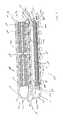
- Substrate 110comprises an elongated dielectric sheet having a first end 107 a and a second end 107 b.
- Substrate 110is desirably flexible and has a plurality of attachment sites 113 on the first side 111 as best seen in FIG. 1 and first contacts 116 and second contacts 114 disposed at or near a second side 112 as best seen in FIG. 2.
- Substrate 110includes a wiring layer with flexible leads 115 extending to the attachment sites 113 . Through holes, vias, or other conductive members extend between the contacts to the flexible leads 115 at or near the first side 111 of the substrate 110 .
- the flexible leads 115have pads 117 exposed at or within the attachment sites 113 . Some of the leads 115 extend between pads 117 and the first contacts 116 and some extend between pads 117 and second contacts 114 . Some leads 115 extend between two pads 117 at two different attachment sites 113 . Some leads extend between first contacts 116 and second contacts 114 . Only a few of the leads 115 are depicted in FIG. 1 for clarity of illustration.
- the flexible leads 115may be routed on the substrate 110 in a variety of ways known to those of ordinary skill in the art.
- the leads 115 shown in FIG. 1are for illustration purposes and the actual configuration of the leads 115 will depend on the microelectronic element or elements to be assembled to the substrate 110 . None of the drawings are to scale and various parts shown may be enlarged for clarity of illustration.
- the substrate 110may be formed from essentially any dielectric material, as for example, one or more layers of a dielectric such as polyimide, BT or flexibilized epoxy.
- the conductive featuressuch as first contacts 116 , second contacts 114 and flexible leads 115 may be formed from conventional metallic materials of the type commonly used in flexible circuitry, as, for example, copper, gold, alloys thereof, or combinations thereof.
- the techniques commonly employed to make flexible circuitrycan be employed to make the substrate 110 and the metallic features thereon. These features may be formed using photolithographic techniques known in the art, by selected deposition such as plating, or by selective removal from a layer as by etching.
- the substratemay include additional features as, for example, one or more additional layers of leads and/or traces and electrically conductive planes such as metallic layers which can serve as a ground or power plane and which cooperate with the leads to form a controlled impedance strip line, or for other purposes.
- a plurality of microelectronic elementsare attached to the attachment sites 113 .
- Each microelectronic element 101may comprise one or more semiconductor chips, circuit panels, microelectronic components, substrates, microelectronic assemblies, stacked assemblies, passive elements, wafers, or combinations thereof. Further, any other components may be incorporated within or on the subassembly. For example, power sources (such as a battery or solar panel), displays (such as LEDs), antennas, speakers, sensors, or other parts may be incorporated within or on the subassembly.
- FIG. 1has four attachment sites 113 for four microelectronic elements: element 101 a , element 101 b, element 101 c, and element 101 d.
- the microelectronic elementseach have a front face 102 , a back face 104 and terminals 103 exposed at the front face 102 . (See FIG. 3A).
- each chipis a memory chip such as a flash memory, DRAM or SRAM.
- the subassembly 100is shown with four microelectronic elements, one or more elements may be used in a subassembly in accordance with embodiments of the invention.
- the microelectronic elementmay have the terminals distributed across the front face 102 in a two-dimensional array, one or more rows of terminals in a central location of the front face 102 , adjacent the periphery of the front face 102 , or in any other configuration.
- Each microelectronic element 101is joined in a flipchip arrangement with the substrate 110 .
- the microelectronic element 101has a “face-down” arrangement with the front face 102 of the chip 101 confronting the first surface 111 of flexible substrate 110 .
- Joining elementsare formed between the pads 117 and the terminals 103 of the microelectronic elements 101 .
- the joining elements 108electrically connect at least some of the terminals 103 on the front face 102 to pads 117 of the leads 115 at the attachment sites 113 .
- the joining elements 108may comprise any electrically conductive material for forming an electrical connection between the conductive pads 117 of the leads 115 on the substrate 110 and the terminals 103 of the microelectronic elements 101 .
- the joining elements 108may comprise a bonding material disposed between pads 117 and terminals 103 .
- Such bonding materialsinclude solder, conductive pastes, and conductive polymers.
- the joining elements 108may comprise leads, wires or other elements, as known in the art.
- the substrate 110 shown in FIG. 3Ashows joining elements 108 connected to pads 117 at first side 111 and the pads 117 are connected to the first contacts or second contacts through vias extending through the substrate 110 .
- the viasare desirably lined or filled with an electrically conductive material, as is known in the art.
- Other methods for forming the first contacts and second contactsare known in the art.
- FIG. 3Ban alternative is shown in which a joining element 108 ′ is disposed between terminal 103 and a pad 117 ′ disposed at the first side 111 .
- a viaextends between the first side 111 and second side 112 of the substrate 110 .
- the viais desirably lined or filled with electrically conductive material.
- the first contact 116 ′may be regarded as incorporating the pad 117 ′, the via, or both, as electrical contact may be made by connecting to any of these features, which are accessible at a side of the substrate 110 .
- FIG. 3Cshows a further embodiment, in which the first contact 116 ′′ comprises a via and a pad 117 ′′ at the second side 112 of the substrate.
- the joining element 108 ′′may be made to extend into the via, so as to form electrical contact with the via, the pad 117 ′′, or both.
- the first contact 116 ′′may be regarded as the via, the pad 117 ′′, or both.
- the leads 115are omitted for at least some of the contacts and the terminals of the microelectronic element are directly connected to a pad, which is connected to the first or second contact. In other embodiments, these connections are routed on the substrate by traces or leads, such as the leads 115 shown in FIG. 1.
- the viasmay be lined with a conductive material or unlined. FIG. 3D shows an unlined via.
- An encapsulant 126at least partially surrounds each microelectronic element, so as to encapsulate the joining elements 108 and the connection between the pads 117 and terminals 103 .
- the encapsulant 126comprises a dielectric material, desirably a thermosetting or thermoplastic polymer, such as an epoxy or an elastomer. A flexibilized epoxy, silicone elastomer, or other compliant or elastomeric material may be used. In other embodiments, more rigid materials are used.
- Encapsulant 126desirably surrounds each microelectronic element 101 .
- the encapsulant 126comprises a flowable material that is dispensed onto the first surface 111 and cured.
- the extent of encapsulant 126is limited so that it will not affect the folding of the substrate.
- methods disclosed in certain embodiments of U.S. Pat. No. 6,225,688, the disclosure of which is hereby incorporated by reference herein,may be used.
- a dammay be placed in the region of the substrate 110 between the microelectronic elements 101 c and 101 d before the encapsulant is dispensed onto the first side 111 .
- the damis desirably removed before folding.
- Other techniques known in the artmay be used.
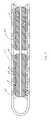
- the substrate 110is folded around axis 105 , so that at least some of microelectronic elements 101 assembled to the substrate 110 are stacked in vertical alignment with one another.
- the microelectronic elementsare grouped in pairs: element 101 a is paired with element 101 b; and element 101 c is paired with element 101 d.
- the substrate 110is folded around fold axis 105 and the paired microelectronic elements are juxtaposed with one another.
- the back faces 104 of the paired microelectronic elementsare desirably positioned close to one another.
- Adhesive 124is desirably disposed on the back faces 104 of the microelectronic elements 101 , adhering the microelectronic elements in a pair together.
- the assembly 100may be made utilizing certain methods disclosed in certain embodiments of U.S. Pat. Nos. 6,121,676 and 6,225,688, the disclosures of which are hereby incorporated by reference herein, as well as certain embodiments of U.S. patent application Ser. No. 09/776,356, the disclosure of which is hereby incorporated by reference herein.
- a variety of methods known in the artmay be used for folding the substrate 110 .
- one or more spacersmay be disposed on the substrate 110 at or near the portion of the substrate 110 to be folded. Such spacer or spacers assist in the folding of the substrate 110 .
- the substrateis folded according to methods disclosed in certain embodiments of provisional application No. 60/408,664, filed Sep. 6, 2002, the disclosure of which is hereby incorporated by reference herein.
- one or more diesare utilized in folding the substrate around an axis of rotation.
- the subassembly 100may include alignment elements formed on portions of the substrate 110 utilizing a mold and encapsulation or over-molding materials.
- the encapsulantis cured in the mold so that the alignment elements are shaped for inter-engagement, as disclosed in certain embodiments of U.S. Provisional Application No. 60/403,939, filed Aug. 16, 2002, the disclosure of which is hereby incorporated by reference herein.
- the alignment elementsUpon folding the substrate, the alignment elements snap together, or engage one another in some manner.
- the folded subassemblyprovides access to second contacts 114 at the top 134 of the subassembly 100 and first contacts 116 at the bottom 136 of the subassembly 100 so that the subassembly 100 may conveniently be connected to other subassemblies or elements, such as packaged or unpackaged microelectronic elements.
- the subassembly 100has an upwardly facing side 120 , and two lateral sides 121 , 122 .
- the ends 107 a and 107 b of the substrate 110are disposed at one lateral side 121 and the fold 118 is disposed at the other lateral side 122 .
- Terms such as top, bottom, upwardly, or downwardlydo not refer to any gravitational frame of reference and are relative to the assembly.
- the substrate 110may be folded to produce subassembly 100 in the shape of an elongated U comprising only one fold 118 .
- other preferred embodimentsmay comprise flexible substrates folded in an S-shape, a zigzag configuration, a spiral, or in other configurations, and more than two microelectronic elements may be stacked vertically in the subassembly.
- the attachment sites 113 on the first side 111 of the flexible substrate 110are preferably spaced so that the substrate can be folded around axis 105 and so that the back faces 104 of the paired elements 101 a and 101 b can be readily juxtaposed with one another during folding.
- the pairs of microelectronic elementsare stacked in back to back configuration.
- a single microelectronic elementis disposed on the substrate, which is folded so as to overlie the back face 104 .
- a second subassembly 200illustrated in FIG. 4, has a flexible substrate 210 with a first surface 211 and a second surface 212 .
- the substratecomprises a dielectric material, an attachment site 213 on first surface 211 , first contacts 216 and second contacts 214 disposed at or near second surface 212 and leads 115 as described above in connection with flexible substrate 110 .
- Second subassembly 200comprises a single microelectronic element 201 .
- the microelectronic element 201comprises any of the microelectronic elements discussed above.
- microelectronic element 201is an integrated circuit, such as a baseband/ASIC large scale integrated circuit.
- Microelectronic element 201has a front face 202 with terminals 203 exposed at the front face 202 and a back face 204 .
- Microelectronic element 201is installed so that front face 202 faces away from the attachment site 213 on the substrate 210 , in a “face-up” arrangement.
- the back face 204confronts the first surface 211 .
- the terminals 103 on the front face 202are attached to the pads 217 of the leads 215 on the substrate by joining elements 108 comprising wire-bonding wires, although other methods of electrical interconnection known in the art may be used.
- microelectronic element 201is attached in a face-down or flip-chip arrangement using attachment methods discussed above with regard to subassembly 100 . Other methods known in the art may be used. Other microelectronic components may be substituted or combined with microelectronic element 201 .
- Microelectronic element 201is desirably attached to the substrate 210 using adhesive 228 disposed between back face 204 and first surface 211 of substrate.
- Microelectronic element 201is desirably encapsulated in an encapsulant material, as discussed above, so that the encapsulant 226 surrounds the microelectronic element 201 and joining elements 208 .
- the encapsulantis desirably formed so as to create a surface 224 overlying the front face 202 .
- Flexible substrate 210is folded to overlie front face 202 .
- the substrate 210is disposed on the surface 224 of encapsulant 226 .
- encapsulant 226forms a layer between front face 202 and the overlying portion of substrate 210 , protecting joining elements 208 .
- the preferred configurations of the subassembly 200provide access to second contacts 214 at the top 234 of the subassembly and first contacts 216 at the bottom 236 of the subassembly, for connection to other elements.
- Flexible substrate 210may be folded to produce a subassembly having an elongated U-shape with a single fold, as illustrated by FIG.
- a subassemblyhas more than one microelectronic element in a face-up arrangement with a folded substrate.
- Such microelectronic elementsmay be electrically connected with leads or other conductive part on the substrate using wire bonding wires, as discussed above.
- first contacts 116 of subassembly 100are electrically connected to second contacts 214 of subassembly 200 .
- a bonding material 258is disposed between contacts 116 and contacts 214 .
- Land grid array (LGA) bondingmay be used.
- at least some of contacts 116are electrically connected to at least some of contacts 214 by solder masses.
- Other methods of connecting contacts of adjacent subassemblies in a stackmay be used, such as ball grid array (BGA) methods, leads, wires or other methods known in the art.
- BGAball grid array
- Use of LGA methodsreduce the overall height of the stack relative to methods such as BGA bonding.
- subassembly 100comprises the top-most subassembly 150 and subassembly 200 comprises the bottom-most subassembly 152 for the assembly.
- subassembly 100comprises the top-most subassembly 150
- subassembly 200comprises the bottom-most subassembly 152 for the assembly.
- more than two subassembliesare used.
- an assemblycomprises the working components of an electronic device.
- the assembly shown in FIG. 4includes an integrated circuit, as well as a series of memory chips.
- Such multi-chip modulesincorporate a number of functions required for an electronic device.
- subassembliesinclude one or more microelectronic elements performing desired functions, and the subassemblies are attached to one another so as to form a partial or a complete electronic device.
- the assemblyis connected to external circuitry using joining units 259 , such as solder balls.
- the joining unitsare disposed at the bottom surface 212 of the folded substrate 210 and are electrically interconnected to the first contacts 216 .
- At least some units 259are connected to at least some of the second contacts 214 .
- at least some of the joining units 259are electrically interconnected with the second contacts 114 exposed on the top 134 of subassembly 100 .
- the present inventionis not limited to the two-subassembly stack illustrated in FIG. 4.
- a larger number of subassemblies including folded substrates, packaged or unpackaged microelectronic elements or other parts,may be included.
- the stackmay be comprised of subassemblies that are identical with each other, or subassemblies having different components or arrangements.
- microelectronic components with or without folded flexible substratesmay be incorporated into the stacked assembly.
- semiconductor chips or other microelectronic elementsmay be attached directly to contacts of a subassembly in a stack.
- components other than folded flexible circuitsmay be incorporated between the subassemblies in the stack.
- a passive componentsuch as lithographic or film-printed circuitry could be stacked between bottom side 136 of subassembly 100 and top side 234 of subassembly 200 with the terminals 116 , 214 exposed on said surfaces attached to the passive circuitry.
- stacked assembliescan be provided which integrate the digital functions of an OEM product into a single microelectronic package and such embodiments are contemplated by the present invention.
- joining elements 308are flexible leads, preferably formed of copper, gold, alloys thereof or combinations thereof. More preferably, joining elements 308 allow the pads 303 on front face 302 to move relative to the pads 317 and attachment sites 313 on first surface 311 . Preferably, joining elements 308 are formed on front face 302 and bonded to the pads 317 . Microelectronic element 301 and flexible substrate 310 are then displaced vertically relative to each other to form S-shaped leads. In other embodiments, the pads 303 exposed on front face 302 may be connected to the pads 317 at the attachment sites 313 by other means known in the art, such as micro-BGA techniques.
- Leadsmay also be formed according to the methods disclosed in commonly assigned U.S. Pat. Nos. 5,148,265; 5,148,266; 5,787,581; and 5,977,618.
- a leadsuch as that illustrated in fragmentary view of FIG. 6 may be employed to further reduce the height of the folded subassembly 100 for chips installed in a face-down configuration.
- joining elements 408comprise leads connected to leads 415 .
- the joining elements 408initially extend over slot 419 in the substrate 410 .
- joining element 408is provided with a notch or other weakened portion therein to provide a frangible portion 406 in the joining element 408 .
- a toolis then inserted into slot 419 to break the joining element 408 and push joining element 408 , making contact with a pad 403 exposed on chip face 402 .
- one or more of the subassembliesincludes a spacer layer disposed between front face and first surface.
- the spacer layeris, preferably, a compliant layer.
- Preferred materials for such compliant layersinclude epoxies and silicones, with flexibilized epoxies and silicone elastomers being particularly preferred.
- the spacer layermay be comprised of a single padded material or, a plurality of pads.
- each subassembly in the stackis provided with a compliant spacer layer to absorb the stress of differential thermal expansion of the flexible substrate relative to microelectronic element and inhibit deformation of the structure during handling and installation of the subassemblies.
- a compliant spacer layerto absorb the stress of differential thermal expansion of the flexible substrate relative to microelectronic element and inhibit deformation of the structure during handling and installation of the subassemblies.
- only the bottom-most subassembly in a stackis provided with a compliant layer, as the effects of differential thermal expansion typically are most critical where the stack contacts external circuitry.
- Such compliant layersmay be provided as disclosed in certain embodiments of U.S. Pat. Nos. 5,679,977; 5,148,266; and 5,148,265, the disclosures of which are hereby incorporated by reference herein.
- the subassembliesmay also comprise a subassembly 500 , as shown as FIG. 7.
- Subassembly 500has a microelectronic element 501 with pads 503 exposed at a front face 502 .
- the microelectronic element 501also has a back face 504 attached to the substrate 510 so that the front face 502 faces away from the substrate 500 .
- the substrateis folded so that a first end 523 and a second end 525 overlie the microelectronic element 501 .
- the ends of the substrate 510are desirably adhered to encapsulant 526 disposed over and around the microelectronic element 501 .
- the subassembly 500includes first contacts 516 at the bottom 536 of the subassembly and second contacts 514 disposed at the top 534 of the subassembly.
- the substrate 510also has leads 515 for forming interconnections, as discussed above. Any of the subassemblies in the assembly may comprise a subassembly 500 , as shown in FIG. 7.
- the subassembly 600may also be used, in certain embodiments.
- Subassembly 600as shown in FIG. 8 comprises a microelectronic element 601 , which is somewhat similar to the microelectronic element 501 shown FIG. 7.
- Subassembly 600also includes microelectronic elements 603 and 605 attached to the second contacts 614 at the top 634 of the subassembly.
- Such microelectronic elementsmay be connected utilizing any of the methods discussed above, or any methods known in the art.
- a bonding materialmay be disposed between pads of the microelectronic elements 603 and 605 and the second contacts 614 .
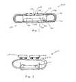
- a subassembly 700may be attached to a single microelectronic element 703 , as shown in FIG. 9A.
- the substratemay have any arrangement.
- a subassembly 700 ′is similar to the subassembly 200 shown in FIG. 4 and is assembled with a single microelectronic element 703 ′.
- One or more packaged or unpackaged microelectronic elementsmay be assembled with any of the subassemblies discussed above. For example, as shown in FIG.
- a pair of microelectronic elements 703 ′′is connected to the subassembly 700 ′′.
- embodiments of the inventionprovide a subassembly that is incorporated into a stacked assembly.
- the subassemblyis desirably arranged or folded so that top contacts are accessible at the top of the subassembly for connection with any packaged or unpackaged microelectronic element or other part, and bottom contacts are accessible at the bottom of the subassembly for connection to external circuitry, to form a stacked microelectronic assembly.
- the substrate of the subassemblyis arranged without substantially increasing the footprint of the microelectronic element, for forming a stacked assembly that conserves space on another component having external circuitry, such as a circuit board.
- two or more subassemblies having folded substratesmay be stacked one on top of the other.
- the first contacts 816are connected to an external element such as a circuit board 851 having terminals 852 .
- the upper-most subassembly 850has second contacts 814 for forming connections with external circuitry, including but not limited to the circuit board 851 .
- the assemblyincludes microelectronic subassemblies comprising subassemblies other than those incorporating folded substrates.
- one or more microelectronic packages or microelectronic partsare connected to the first contacts and/or second contacts of one or more subassemblies in the assembly.
- a microelectronic package or microelectronic partmay be interposed between a subassembly having a folded substrate and either another subassembly having a folded substrate or another microelectronic package or microelectronic part.
- Such assemblesmay be mounted on a circuit board, as disclosed in certain embodiments of U.S. Provisional Application No. 60/408,644, filed Sep.
- Assemblies in accordance with embodiments of the present inventionmay be utilized in methods of operating a circuit board stuffing production plant, and/or methods of making a circuit board assembly, as disclosed in certain embodiments of U.S. Provisional Application No. 60/408,644, filed Sep. 6, 2002, the disclosure of which is hereby incorporated by reference herein.
Landscapes
- Engineering & Computer Science (AREA)
- Microelectronics & Electronic Packaging (AREA)
- Power Engineering (AREA)
- Physics & Mathematics (AREA)
- Condensed Matter Physics & Semiconductors (AREA)
- General Physics & Mathematics (AREA)
- Computer Hardware Design (AREA)
- Wire Bonding (AREA)
Abstract
Description
- This application is a continuation-in-part of application Ser. No. 09/776,356, filed Feb. 2, 2001, which is a divisional of application Ser. No. 09/244,581, filed Feb. 4, 1999, which is a continuation-in-part of application Ser. No. 08/987,569, filed Dec. 11, 1997, now U.S. Pat. No. 6,121,676, claiming benefit of Provisional Application No. 60/033,353, filed Dec. 13, 1996, the disclosures of which are all hereby incorporated by reference herein. This application also claims benefit of Provisional Application No. 60/343,821, filed Oct. 26, 2001, the disclosure of which is hereby incorporated by reference herein.[0001]
- The present invention relates to microelectronic assemblies and, in particular, assemblies wherein a number of subassemblies are stacked one on top of another to form the microelectronic assembly.[0002]
- Certain microelectronic packages are made using a sheet-like element incorporating a dielectric layer and mounting terminals disposed on the element. Some or all of the terminals are connected to a microelectronic device which is assembled with the sheet-like element in a package. Various proposals have been advanced for stacking plural chips one above the other in a common package. One such arrangement includes a substrate having a dielectric structure substantially larger in area than the area of a single microelectronic device or chip. Several microelectronic devices are mounted to the substrate in different areas of the substrate and the substrate is folded so that the various microelectronic devices are stacked one above the other and so that the mounting terminals on the substrate are disposed at the bottom of the stack. Typically, the substrate has electrically conductive traces extending along the dielectric structure. These traces connect the microelectronic devices with one another, with the mounting terminals, or both, in the completed structure.[0003]
- The substrate must be folded in precisely the right configuration so that the various microelectronic devices will be disposed in the correct locations, one above the other. The entire package could be placed in an area of a circuit board only slightly larger than the area occupied by a single microelectronic device. However, inaccuracies in folding the substrate can cause parts of the package to lie in positions different from their intended position relative to the mounting terminals. This effectively increases the overall size of the package. Neighboring components mounted to the circuit board must be located at a larger distance from the stack so as to provide clearance sufficient to accommodate this internal misalignment within the stack. Moreover, the piece-to-piece differences between individual packages caused by folding inaccuracies can complicate the task of handling and feeding the stacked packages during automated assembly operation as, for example, during mounting to the circuit panel.[0004]
- It is desirable to provide further improvements in stacked microelectronic assemblies and methods of forming the same.[0005]
- In one aspect of the present invention, a stacked microelectronic assembly comprises a plurality of microelectronic subassemblies. Each subassembly comprises a substrate having at least one attachment site, a plurality of first contacts, and a plurality of second contacts. At least one microelectronic element is assembled to the at least one attachment site and electrically connected to at least some of the first and second contacts. The substrate is folded so that the first contacts are accessible at a bottom of the subassembly and the second contacts are accessible at a top of the subassembly. The plurality of subassemblies are stacked one on top of another substantially vertically so that an upper subassembly is adjacent a lower subassembly. At least some of the first contacts of the upper subassembly are connected to at least some of the second contacts of the lower subassembly. The individual subassemblies may comprise one or more components having various functions and the subassemblies need not be identical to each other.[0006]
- Embodiments of the invention provide assemblies having a plurality of subassemblies stacked one on top of another. Each subassembly desirably has a separate substrate, alleviating many alignment problems. A plurality of subassemblies having microelectronic elements of a certain type may be made and assembled with subassemblies of a different type so as to form a module.[0007]
- Each subassembly may include more than one microelectronic element on a substrate. In certain embodiments, the substrate of at least one of the subassemblies comprises a plurality of attachment sites and a plurality of microelectronic elements is assembled to the attachment sites.[0008]
- The substrate of the at least one subassembly may be folded so that at least some of said plurality of microelectronic elements are stacked in substantially vertical alignment with one another. The microelectronic elements may include a first microelectronic element and a second microelectronic element. Each of the microelectronic elements has a first side facing the attachment site to which the microelectronic element is assembled and a second side, opposite the first side. The second sides of the microelectronic elements may be adhered to one another.[0009]
- The substrate may be folded so that at least some of the plurality of microelectronic elements are disposed alongside one another. In certain preferred embodiments, the plurality of microelectronic elements comprises a plurality of memory chips. In certain preferred embodiments, the at least one microelectronic element comprises an application scale integrated circuit.[0010]
- In certain embodiments, the assembly includes a passive electronic component. For example, the passive electronic component may be electrically connected with at least some of the first contacts and/or the second contacts. The passive electronic component may be interposed between a first subassembly of the plurality of subassemblies and a second subassembly of the plurality of subassemblies. The passive electronic component may be electrically interconnected with at least some of the first contacts of the first subassembly and at least some of the second contacts of the second subassembly. In other embodiments, a passive component is incorporated in one of the subassemblies.[0011]
- In certain preferred embodiments, the assembly comprises components performing several different functions of an electronic device. For example, the assembly may comprise an integration of substantially all of the digital functions of a wireless telecommunications device.[0012]
- In certain embodiments, a first subassembly of the plurality of subassemblies comprises at least one memory chip. A second subassembly of said plurality of subassemblies may comprise a large scale integrated circuit. The subassemblies may include any electronic component or part, including digital, RF, or analog parts.[0013]
- In certain embodiments, each subassembly has a plurality of leads electrically interconnected to at least some of the first and second contacts. In certain embodiments, the at least one microelectronic element has a first side with a plurality of pads exposed at the first side, and a second side opposite from the first side. For example, the first side may face away from the attachment site to which the microelectronic element is assembled and the pads may be connected to the leads by wire bonding wires. In another example, the first side may face the attachment site to which the microelectronic element is assembled and a bonding material may connect the leads and the pads.[0014]
- The subassemblies desirably comprise a first subassembly having a first substrate and a second subassembly having a second substrate, the first substrate being separate from the second substrate.[0015]
- The substrate of at least one of the subassemblies desirably carries interengaging elements for holding the substrate in a folded arrangement.[0016]
- In certain embodiments, at least one of the subassemblies has a substrate with a single fold on one side of said subassembly. In other embodiments, at least one of the subassemblies has a substrate with a first fold on one side of said subassembly and a second fold on the other side of said subassembly.[0017]
- A microelectronic element may be connected to the second contacts of the top-most subassembly.[0018]
- In certain embodiments, each subassembly has a plurality of leads electrically interconnected to at least some of the first and second contacts. The leads of at least one of the subassemblies desirably include leads extending between the first contacts and the attachment sites. The leads may include leads extending between two of the attachment sites. The leads may include leads extending between the second contacts and the attachment sites. The leads may also include leads extending between the first contacts and the second contacts.[0019]
- The subassemblies desirably include a bottom-most subassembly and a top-most subassembly. The first contacts of the bottom-most subassembly are accessible at a bottom of the assembly and the second contacts of the top-most subassembly are accessible at a top of the subassembly.[0020]
- In a further aspect of the present invention, a stacked microelectronic assembly comprises a plurality of microelectronic subassemblies. Each subassembly comprises a substrate having at least one attachment site, a first end, a second end, and a plurality of contacts. At least one microelectronic element is assembled to the at least one attachment site and electrically connected to at least some of the contacts, and the substrate is folded. The plurality of subassemblies is stacked one on top of another substantially vertically.[0021]
- The subassemblies may comprise a first subassembly having a first substrate and a second subassembly having a second substrate. The first substrate is desirably separate from said second substrate.[0022]
- The first end and second end of the substrate, in certain embodiments, are disposed at an upwardly facing side of the subassembly. In other embodiments, the first end and second end are disposed at a lateral side of the subassembly.[0023]
- These and other features, aspects, and advantages of the present invention will become better understood with regard to the following description, appended claims and accompanying drawings where:[0024]
- FIG. 1 is a schematic top plan view of a flexible substrate for an assembly in accordance with an embodiment of the invention;[0025]
- FIG. 2 is a schematic bottom second plan view of a flexible substrate for an assembly in accordance with the embodiment of FIG. 1;[0026]
- FIG. 3A is a cross-sectional view of a subassembly in accordance with the embodiment of FIGS. 1 and 2;[0027]
- FIG. 3B is a partial cross-sectional view of a subassembly in accordance with a further embodiment of the invention;[0028]
- FIG. 3C is a partial cross-sectional view of a subassembly in accordance with another embodiment of the invention;[0029]
- FIG. 3D is a partial cross-sectional view of a subassembly in accordance with another embodiment of the invention;[0030]
- FIG. 4 is a cross-sectional view of an assembly in accordance with the embodiment of FIGS.[0031]1-3A;
- FIG. 5 is a cross-sectional view of a subassembly in accordance with a further embodiment of the invention;[0032]
- FIG. 6 is a partial cross-sectional view of a subassembly in accordance with a further embodiment of the invention;[0033]
- FIG. 7 is a cross-sectional view of a subassembly in accordance with another embodiment of the invention;[0034]
- FIG. 8 is a cross-sectional view of subassembly in accordance with a further embodiment of the invention;[0035]
- FIG. 9A is a cross-sectional view of an assembly in accordance with another embodiment of the invention;[0036]
- FIG. 9B is a cross-sectional view of an assembly in accordance with another embodiment of the invention;[0037]
- FIG. 9C is a cross-sectional view of an assembly in accordance with another embodiment of the invention; and[0038]
- FIG. 10 is a cross-sectional view of an assembly in accordance with a further embodiment of the invention.[0039]
- An embodiment of the invention is shown in FIGS.[0040]1-3A and4.
Substrate 110 comprises an elongated dielectric sheet having afirst end 107aand a second end107b.Substrate 110 is desirably flexible and has a plurality ofattachment sites 113 on the first side111 as best seen in FIG. 1 andfirst contacts 116 andsecond contacts 114 disposed at or near asecond side 112 as best seen in FIG. 2.Substrate 110 includes a wiring layer withflexible leads 115 extending to theattachment sites 113. Through holes, vias, or other conductive members extend between the contacts to the flexible leads115 at or near the first side111 of thesubstrate 110. The flexible leads115 havepads 117 exposed at or within theattachment sites 113. Some of theleads 115 extend betweenpads 117 and thefirst contacts 116 and some extend betweenpads 117 andsecond contacts 114. Some leads115 extend between twopads 117 at twodifferent attachment sites 113. Some leads extend betweenfirst contacts 116 andsecond contacts 114. Only a few of theleads 115 are depicted in FIG. 1 for clarity of illustration. The flexible leads115 may be routed on thesubstrate 110 in a variety of ways known to those of ordinary skill in the art. The leads115 shown in FIG. 1 are for illustration purposes and the actual configuration of theleads 115 will depend on the microelectronic element or elements to be assembled to thesubstrate 110. None of the drawings are to scale and various parts shown may be enlarged for clarity of illustration. - The[0041]
substrate 110 may be formed from essentially any dielectric material, as for example, one or more layers of a dielectric such as polyimide, BT or flexibilized epoxy. The conductive features such asfirst contacts 116,second contacts 114 andflexible leads 115 may be formed from conventional metallic materials of the type commonly used in flexible circuitry, as, for example, copper, gold, alloys thereof, or combinations thereof. The techniques commonly employed to make flexible circuitry can be employed to make thesubstrate 110 and the metallic features thereon. These features may be formed using photolithographic techniques known in the art, by selected deposition such as plating, or by selective removal from a layer as by etching. The substrate may include additional features as, for example, one or more additional layers of leads and/or traces and electrically conductive planes such as metallic layers which can serve as a ground or power plane and which cooperate with the leads to form a controlled impedance strip line, or for other purposes. - A plurality of microelectronic elements are attached to the[0042]
attachment sites 113. Eachmicroelectronic element 101 may comprise one or more semiconductor chips, circuit panels, microelectronic components, substrates, microelectronic assemblies, stacked assemblies, passive elements, wafers, or combinations thereof. Further, any other components may be incorporated within or on the subassembly. For example, power sources (such as a battery or solar panel), displays (such as LEDs), antennas, speakers, sensors, or other parts may be incorporated within or on the subassembly. - The embodiment illustrated in FIG. 1 has four[0043]
attachment sites 113 for four microelectronic elements: element101a, element101b,element101c,and element101d.The microelectronic elements each have afront face 102, a back face104 andterminals 103 exposed at thefront face 102. (See FIG. 3A). In certain embodiments, each chip is a memory chip such as a flash memory, DRAM or SRAM. Although thesubassembly 100 is shown with four microelectronic elements, one or more elements may be used in a subassembly in accordance with embodiments of the invention. The microelectronic element may have the terminals distributed across thefront face 102 in a two-dimensional array, one or more rows of terminals in a central location of thefront face 102, adjacent the periphery of thefront face 102, or in any other configuration. - Each[0044]
microelectronic element 101 is joined in a flipchip arrangement with thesubstrate 110. Themicroelectronic element 101 has a “face-down” arrangement with thefront face 102 of thechip 101 confronting the first surface111 offlexible substrate 110. Joining elements are formed between thepads 117 and theterminals 103 of themicroelectronic elements 101. The joiningelements 108 electrically connect at least some of theterminals 103 on thefront face 102 topads 117 of theleads 115 at theattachment sites 113. - The joining[0045]
elements 108 may comprise any electrically conductive material for forming an electrical connection between theconductive pads 117 of theleads 115 on thesubstrate 110 and theterminals 103 of themicroelectronic elements 101. For example, as shown in FIG. 3A, the joiningelements 108 may comprise a bonding material disposed betweenpads 117 andterminals 103. Such bonding materials include solder, conductive pastes, and conductive polymers. The joiningelements 108 may comprise leads, wires or other elements, as known in the art. - The[0046]
substrate 110 shown in FIG. 3A shows joiningelements 108 connected topads 117 at first side111 and thepads 117 are connected to the first contacts or second contacts through vias extending through thesubstrate 110. The vias are desirably lined or filled with an electrically conductive material, as is known in the art. Other methods for forming the first contacts and second contacts are known in the art. For example, an alternative is shown in FIG. 3B, in which a joiningelement 108′ is disposed betweenterminal 103 and apad 117′ disposed at the first side111. A via extends between the first side111 andsecond side 112 of thesubstrate 110. The via is desirably lined or filled with electrically conductive material. Thefirst contact 116′ may be regarded as incorporating thepad 117′, the via, or both, as electrical contact may be made by connecting to any of these features, which are accessible at a side of thesubstrate 110. FIG. 3C shows a further embodiment, in which thefirst contact 116″ comprises a via and apad 117″ at thesecond side 112 of the substrate. The joiningelement 108″ may be made to extend into the via, so as to form electrical contact with the via, thepad 117″, or both. Thefirst contact 116″ may be regarded as the via, thepad 117″, or both. In further embodiments, theleads 115 are omitted for at least some of the contacts and the terminals of the microelectronic element are directly connected to a pad, which is connected to the first or second contact. In other embodiments, these connections are routed on the substrate by traces or leads, such as theleads 115 shown in FIG. 1. The vias may be lined with a conductive material or unlined. FIG. 3D shows an unlined via. - An[0047]
encapsulant 126 at least partially surrounds each microelectronic element, so as to encapsulate the joiningelements 108 and the connection between thepads 117 andterminals 103. Theencapsulant 126 comprises a dielectric material, desirably a thermosetting or thermoplastic polymer, such as an epoxy or an elastomer. A flexibilized epoxy, silicone elastomer, or other compliant or elastomeric material may be used. In other embodiments, more rigid materials are used.Encapsulant 126 desirably surrounds eachmicroelectronic element 101. Preferably, theencapsulant 126 comprises a flowable material that is dispensed onto the first surface111 and cured. Preferably, the extent ofencapsulant 126 is limited so that it will not affect the folding of the substrate. For example, methods disclosed in certain embodiments of U.S. Pat. No. 6,225,688, the disclosure of which is hereby incorporated by reference herein, may be used. A dam may be placed in the region of thesubstrate 110 between the microelectronic elements101cand101dbefore the encapsulant is dispensed onto the first side111. The dam is desirably removed before folding. Other techniques known in the art may be used. - After[0048]
microelectronic elements 101 have been attached to thesubstrate 110 and encapsulated, thesubstrate 110 is folded around axis105, so that at least some ofmicroelectronic elements 101 assembled to thesubstrate 110 are stacked in vertical alignment with one another. In the embodiment shown in FIG. 3A, the microelectronic elements are grouped in pairs: element101ais paired with element101b; and element101cis paired with element101d.Thesubstrate 110 is folded around fold axis105 and the paired microelectronic elements are juxtaposed with one another. The back faces104 of the paired microelectronic elements are desirably positioned close to one another. By vertically aligning at least some of the microelectronic elements in close proximity with one another, the size of the stacked assembly will be minimized. Adhesive124 is desirably disposed on the back faces104 of themicroelectronic elements 101, adhering the microelectronic elements in a pair together. - The[0049]
assembly 100 may be made utilizing certain methods disclosed in certain embodiments of U.S. Pat. Nos. 6,121,676 and 6,225,688, the disclosures of which are hereby incorporated by reference herein, as well as certain embodiments of U.S. patent application Ser. No. 09/776,356, the disclosure of which is hereby incorporated by reference herein. - A variety of methods known in the art may be used for folding the[0050]
substrate 110. For example, as disclosed in certain embodiments of U.S. Pat. No. 6,225,688, the disclosure of which is hereby incorporated by reference herein, one or more spacers may be disposed on thesubstrate 110 at or near the portion of thesubstrate 110 to be folded. Such spacer or spacers assist in the folding of thesubstrate 110. In further embodiments of the invention, the substrate is folded according to methods disclosed in certain embodiments of provisional application No. 60/408,664, filed Sep. 6, 2002, the disclosure of which is hereby incorporated by reference herein. For example, one or more dies are utilized in folding the substrate around an axis of rotation. In addition, thesubassembly 100 may include alignment elements formed on portions of thesubstrate 110 utilizing a mold and encapsulation or over-molding materials. The encapsulant is cured in the mold so that the alignment elements are shaped for inter-engagement, as disclosed in certain embodiments of U.S. Provisional Application No. 60/403,939, filed Aug. 16, 2002, the disclosure of which is hereby incorporated by reference herein. Upon folding the substrate, the alignment elements snap together, or engage one another in some manner. - The folded subassembly, as shown in FIG. 4, provides access to[0051]
second contacts 114 at the top134 of thesubassembly 100 andfirst contacts 116 at the bottom136 of thesubassembly 100 so that thesubassembly 100 may conveniently be connected to other subassemblies or elements, such as packaged or unpackaged microelectronic elements. Thesubassembly 100 has an upwardly facingside 120, and twolateral sides ends 107aand107bof thesubstrate 110 are disposed at onelateral side 121 and thefold 118 is disposed at the otherlateral side 122. However, other arrangements are within the scope of the present invention. Terms such as top, bottom, upwardly, or downwardly do not refer to any gravitational frame of reference and are relative to the assembly. - As illustrated in FIG. 3A, the[0052]
substrate 110 may be folded to producesubassembly 100 in the shape of an elongated U comprising only onefold 118. As disclosed in commonly assigned U.S. patent application Ser. No. 09/776,356, and U.S. Pat. Nos. 6,121,676 and 6,225,688, the disclosures of which are all hereby incorporated by reference herein, other preferred embodiments may comprise flexible substrates folded in an S-shape, a zigzag configuration, a spiral, or in other configurations, and more than two microelectronic elements may be stacked vertically in the subassembly. - In embodiments that comprise paired microelectronic elements, such as chips[0053]101a,and101b,and/or101cand101d,the
attachment sites 113 on the first side111 of theflexible substrate 110 are preferably spaced so that the substrate can be folded around axis105 and so that the back faces104 of the paired elements101aand101bcan be readily juxtaposed with one another during folding. In the embodiment shown in FIG. 3A, the pairs of microelectronic elements are stacked in back to back configuration. However, in other preferred embodiments, a single microelectronic element is disposed on the substrate, which is folded so as to overlie the back face104. - A[0054]
second subassembly 200, illustrated in FIG. 4, has aflexible substrate 210 with afirst surface 211 and asecond surface 212. The substrate comprises a dielectric material, an attachment site213 onfirst surface 211, first contacts216 and second contacts214 disposed at or nearsecond surface 212 and leads115 as described above in connection withflexible substrate 110.Second subassembly 200 comprises a singlemicroelectronic element 201. Themicroelectronic element 201 comprises any of the microelectronic elements discussed above. In certain preferred embodiments,microelectronic element 201 is an integrated circuit, such as a baseband/ASIC large scale integrated circuit.Microelectronic element 201 has afront face 202 withterminals 203 exposed at thefront face 202 and aback face 204.Microelectronic element 201 is installed so thatfront face 202 faces away from the attachment site213 on thesubstrate 210, in a “face-up” arrangement. Theback face 204 confronts thefirst surface 211. In this configuration, theterminals 103 on thefront face 202 are attached to thepads 217 of theleads 215 on the substrate by joiningelements 108 comprising wire-bonding wires, although other methods of electrical interconnection known in the art may be used. In other preferred embodiments,microelectronic element 201 is attached in a face-down or flip-chip arrangement using attachment methods discussed above with regard tosubassembly 100. Other methods known in the art may be used. Other microelectronic components may be substituted or combined withmicroelectronic element 201. - [0055]
Microelectronic element 201 is desirably attached to thesubstrate 210 using adhesive228 disposed betweenback face 204 andfirst surface 211 of substrate.Microelectronic element 201 is desirably encapsulated in an encapsulant material, as discussed above, so that theencapsulant 226 surrounds themicroelectronic element 201 and joiningelements 208. The encapsulant is desirably formed so as to create asurface 224 overlying thefront face 202. - [0056]
Flexible substrate 210 is folded to overliefront face 202. Desirably, thesubstrate 210 is disposed on thesurface 224 ofencapsulant 226. In preferred embodiments, encapsulant226 forms a layer betweenfront face 202 and the overlying portion ofsubstrate 210, protecting joiningelements 208. The preferred configurations of thesubassembly 200 provide access to second contacts214 at the top234 of the subassembly and first contacts216 at the bottom236 of the subassembly, for connection to other elements.Flexible substrate 210 may be folded to produce a subassembly having an elongated U-shape with a single fold, as illustrated by FIG. 4, or in other configurations such as a S-shape, zigzag stack or spiral and may include one or more microelectronic elements attached to thesubstrate 210 in a variety of ways. In certain embodiments, a subassembly has more than one microelectronic element in a face-up arrangement with a folded substrate. Such microelectronic elements may be electrically connected with leads or other conductive part on the substrate using wire bonding wires, as discussed above. - In a preferred embodiment illustrated by FIG. 4,[0057]
first contacts 116 ofsubassembly 100 are electrically connected to second contacts214 ofsubassembly 200. For example, abonding material 258 is disposed betweencontacts 116 and contacts214. Land grid array (LGA) bonding may be used. For example, at least some ofcontacts 116 are electrically connected to at least some of contacts214 by solder masses. Other methods of connecting contacts of adjacent subassemblies in a stack may be used, such as ball grid array (BGA) methods, leads, wires or other methods known in the art. Use of LGA methods reduce the overall height of the stack relative to methods such as BGA bonding. In a preferred embodiment, two subassemblies are used, and the assembly has an overall thickness of 1.2 mm or less. In the embodiment shown,subassembly 100 comprises thetop-most subassembly 150 andsubassembly 200 comprises thebottom-most subassembly 152 for the assembly. However, in other embodiments, more than two subassemblies are used. - In certain preferred embodiments, an assembly comprises the working components of an electronic device. For example, the assembly shown in FIG. 4 includes an integrated circuit, as well as a series of memory chips. Such multi-chip modules incorporate a number of functions required for an electronic device. In certain preferred embodiments, subassemblies include one or more microelectronic elements performing desired functions, and the subassemblies are attached to one another so as to form a partial or a complete electronic device.[0058]
- The assembly is connected to external circuitry using joining[0059]
units 259, such as solder balls. The joining units are disposed at thebottom surface 212 of the foldedsubstrate 210 and are electrically interconnected to the first contacts216. At least someunits 259 are connected to at least some of the second contacts214. Moreover, at least some of the joiningunits 259 are electrically interconnected with thesecond contacts 114 exposed on the top134 ofsubassembly 100. - The present invention is not limited to the two-subassembly stack illustrated in FIG. 4. A larger number of subassemblies including folded substrates, packaged or unpackaged microelectronic elements or other parts, may be included. The stack may be comprised of subassemblies that are identical with each other, or subassemblies having different components or arrangements. Moreover, in certain preferred embodiments, microelectronic components with or without folded flexible substrates may be incorporated into the stacked assembly. For example, semiconductor chips or other microelectronic elements may be attached directly to contacts of a subassembly in a stack. Moreover, components other than folded flexible circuits may be incorporated between the subassemblies in the stack. For example, a passive component such as lithographic or film-printed circuitry could be stacked between[0060]
bottom side 136 ofsubassembly 100 andtop side 234 ofsubassembly 200 with theterminals 116,214 exposed on said surfaces attached to the passive circuitry. By combining folded flexible circuit subassemblies with selected active and passive components, stacked assemblies can be provided which integrate the digital functions of an OEM product into a single microelectronic package and such embodiments are contemplated by the present invention. - In a further embodiment shown in FIG. 5, joining[0061]
elements 308 are flexible leads, preferably formed of copper, gold, alloys thereof or combinations thereof. More preferably, joiningelements 308 allow thepads 303 onfront face 302 to move relative to thepads 317 andattachment sites 313 onfirst surface 311. Preferably, joiningelements 308 are formed onfront face 302 and bonded to thepads 317.Microelectronic element 301 andflexible substrate 310 are then displaced vertically relative to each other to form S-shaped leads. In other embodiments, thepads 303 exposed onfront face 302 may be connected to thepads 317 at theattachment sites 313 by other means known in the art, such as micro-BGA techniques. Examples of preferred types of leads and methods for making the same are disclosed in commonly assigned U.S. Pat. Nos. 6,228,686; 6,191,368; 5,976,913; 5,859,472; 5,518,964; and in co-pending commonly assigned U.S. patent application Ser. No. 08/715,571. - Leads may also be formed according to the methods disclosed in commonly assigned U.S. Pat. Nos. 5,148,265; 5,148,266; 5,787,581; and 5,977,618. A lead such as that illustrated in fragmentary view of FIG. 6 may be employed to further reduce the height of the folded[0062]
subassembly 100 for chips installed in a face-down configuration. In general, joining elements408 comprise leads connected to leads415. The joining elements408 initially extend over slot419 in thesubstrate 410. In a preferred method, joining element408 is provided with a notch or other weakened portion therein to provide afrangible portion 406 in the joining element408. A tool is then inserted into slot419 to break the joining element408 and push joining element408, making contact with apad 403 exposed onchip face 402. - In certain preferred embodiments, one or more of the subassemblies includes a spacer layer disposed between front face and first surface. The spacer layer is, preferably, a compliant layer. Preferred materials for such compliant layers include epoxies and silicones, with flexibilized epoxies and silicone elastomers being particularly preferred. The spacer layer may be comprised of a single padded material or, a plurality of pads.[0063]
- In certain preferred embodiments, each subassembly in the stack is provided with a compliant spacer layer to absorb the stress of differential thermal expansion of the flexible substrate relative to microelectronic element and inhibit deformation of the structure during handling and installation of the subassemblies. In other preferred embodiments of the invention, only the bottom-most subassembly in a stack is provided with a compliant layer, as the effects of differential thermal expansion typically are most critical where the stack contacts external circuitry. Such compliant layers may be provided as disclosed in certain embodiments of U.S. Pat. Nos. 5,679,977; 5,148,266; and 5,148,265, the disclosures of which are hereby incorporated by reference herein.[0064]
- The subassemblies may also comprise a[0065]
subassembly 500, as shown as FIG. 7.Subassembly 500 has amicroelectronic element 501 withpads 503 exposed at afront face 502. Themicroelectronic element 501 also has aback face 504 attached to thesubstrate 510 so that thefront face 502 faces away from thesubstrate 500. The substrate is folded so that afirst end 523 and asecond end 525 overlie themicroelectronic element 501. The ends of thesubstrate 510 are desirably adhered to encapsulant526 disposed over and around themicroelectronic element 501. Thesubassembly 500 includesfirst contacts 516 at the bottom536 of the subassembly andsecond contacts 514 disposed at the top534 of the subassembly. Thesubstrate 510 also hasleads 515 for forming interconnections, as discussed above. Any of the subassemblies in the assembly may comprise asubassembly 500, as shown in FIG. 7. - The subassembly[0066]600 may also be used, in certain embodiments. Subassembly600, as shown in FIG. 8 comprises a
microelectronic element 601, which is somewhat similar to themicroelectronic element 501 shown FIG. 7. Subassembly600 also includesmicroelectronic elements microelectronic elements - In addition, a[0067]
subassembly 700 may be attached to a singlemicroelectronic element 703, as shown in FIG. 9A. Although thesubassembly 700 shown in FIG. 9A has the ends of the substrate disposed at an upper side of thesubassembly 700, the substrate may have any arrangement. For example, in FIG. 9B, asubassembly 700′ is similar to thesubassembly 200 shown in FIG. 4 and is assembled with a singlemicroelectronic element 703′. One or more packaged or unpackaged microelectronic elements may be assembled with any of the subassemblies discussed above. For example, as shown in FIG. 9C, a pair ofmicroelectronic elements 703″ is connected to thesubassembly 700″. Thus, embodiments of the invention provide a subassembly that is incorporated into a stacked assembly. The subassembly is desirably arranged or folded so that top contacts are accessible at the top of the subassembly for connection with any packaged or unpackaged microelectronic element or other part, and bottom contacts are accessible at the bottom of the subassembly for connection to external circuitry, to form a stacked microelectronic assembly. Desirably, the substrate of the subassembly is arranged without substantially increasing the footprint of the microelectronic element, for forming a stacked assembly that conserves space on another component having external circuitry, such as a circuit board. - As shown in FIG. 10, two or more subassemblies having folded substrates may be stacked one on top of the other. The[0068]
first contacts 816 are connected to an external element such as acircuit board 851 havingterminals 852. Theupper-most subassembly 850 hassecond contacts 814 for forming connections with external circuitry, including but not limited to thecircuit board 851. - In further embodiments, the assembly includes microelectronic subassemblies comprising subassemblies other than those incorporating folded substrates. For example, one or more microelectronic packages or microelectronic parts are connected to the first contacts and/or second contacts of one or more subassemblies in the assembly. A microelectronic package or microelectronic part may be interposed between a subassembly having a folded substrate and either another subassembly having a folded substrate or another microelectronic package or microelectronic part. Such assembles may be mounted on a circuit board, as disclosed in certain embodiments of U.S. Provisional Application No. 60/408,644, filed Sep. 6, 2002, the disclosure of which is hereby incorporated by reference herein. Assemblies in accordance with embodiments of the present invention may be utilized in methods of operating a circuit board stuffing production plant, and/or methods of making a circuit board assembly, as disclosed in certain embodiments of U.S. Provisional Application No. 60/408,644, filed Sep. 6, 2002, the disclosure of which is hereby incorporated by reference herein.[0069]
- Although the invention herein has been described with reference to particular embodiments, it is to be understood that these embodiments are merely illustrative of the principles and applications of the present invention. It is therefore to be understood that numerous modifications may be made to the illustrative embodiments and that other arrangements may be devised without departing from the spirit and scope of the present invention as described herein or the exemplary claims which follow.[0070]
Claims (34)
Priority Applications (1)
| Application Number | Priority Date | Filing Date | Title |
|---|---|---|---|
| US10/281,550US7149095B2 (en) | 1996-12-13 | 2002-10-28 | Stacked microelectronic assemblies |
Applications Claiming Priority (6)
| Application Number | Priority Date | Filing Date | Title |
|---|---|---|---|
| US3335396P | 1996-12-13 | 1996-12-13 | |
| US08/987,569US6121676A (en) | 1996-12-13 | 1997-12-11 | Stacked microelectronic assembly and method therefor |
| US09/244,581US6225688B1 (en) | 1997-12-11 | 1999-02-04 | Stacked microelectronic assembly and method therefor |
| US09/776,356US6699730B2 (en) | 1996-12-13 | 2001-02-02 | Stacked microelectronic assembly and method therefor |
| US34382101P | 2001-10-26 | 2001-10-26 | |
| US10/281,550US7149095B2 (en) | 1996-12-13 | 2002-10-28 | Stacked microelectronic assemblies |
Related Parent Applications (1)
| Application Number | Title | Priority Date | Filing Date |
|---|---|---|---|
| US09/776,356Continuation-In-PartUS6699730B2 (en) | 1996-12-13 | 2001-02-02 | Stacked microelectronic assembly and method therefor |
Publications (2)
| Publication Number | Publication Date |
|---|---|
| US20030168725A1true US20030168725A1 (en) | 2003-09-11 |
| US7149095B2 US7149095B2 (en) | 2006-12-12 |
Family
ID=27792333
Family Applications (1)
| Application Number | Title | Priority Date | Filing Date |
|---|---|---|---|
| US10/281,550Expired - Fee RelatedUS7149095B2 (en) | 1996-12-13 | 2002-10-28 | Stacked microelectronic assemblies |
Country Status (1)
| Country | Link |
|---|---|
| US (1) | US7149095B2 (en) |
Cited By (94)
| Publication number | Priority date | Publication date | Assignee | Title |
|---|---|---|---|---|
| US20020162215A1 (en)* | 2001-03-14 | 2002-11-07 | Kledzik Kenneth J. | Method and apparatus for fabricating a circuit board with a three dimensional surface mounted array of semiconductor chips |
| US20020193139A1 (en)* | 2001-03-30 | 2002-12-19 | Gunnar Mildh | Network/cell/interface selection in mixed networks |
| US20030165051A1 (en)* | 2000-03-13 | 2003-09-04 | Kledzik Kenneth J. | Modular integrated circuit chip carrier |
| US20030197283A1 (en)* | 2002-04-23 | 2003-10-23 | Shin Choi | Multi-chip package and method for manufacturing the same |
| US20030198032A1 (en)* | 2002-04-23 | 2003-10-23 | Paul Collander | Integrated circuit assembly and method for making same |
| US20030201525A1 (en)* | 2002-04-25 | 2003-10-30 | Micron Technology, Inc. | Standoffs for centralizing internals in packaging process |
| US20030234443A1 (en)* | 2001-10-26 | 2003-12-25 | Staktek Group, L.P. | Low profile stacking system and method |
| US20040048418A1 (en)* | 2000-09-29 | 2004-03-11 | Tessera, Inc. | Low cost and compliant microelectronic packages for high I/O and fine pitch |
| US20040108590A1 (en)* | 2000-10-16 | 2004-06-10 | Kledzik Kenneth J. | Carrier-based electronic module |
| US20040126050A1 (en)* | 2002-12-30 | 2004-07-01 | Claydon Glenn Scott | Assembly, contact and coupling interconnection for optoelectronics |
| US20040150107A1 (en)* | 2002-12-31 | 2004-08-05 | Cha Ki Bon | Stack package and fabricating method thereof |
| US20040176924A1 (en)* | 2003-03-07 | 2004-09-09 | Salmon Peter C. | Apparatus and method for testing electronic systems |
| US20040178496A1 (en)* | 2001-10-26 | 2004-09-16 | Staktek Grop, L.P. | Memory expansion and chip scale stacking system and method |
| US20050040513A1 (en)* | 2003-08-20 | 2005-02-24 | Salmon Peter C. | Copper-faced modules, imprinted copper circuits, and their application to supercomputers |
| US20050067688A1 (en)* | 2003-09-26 | 2005-03-31 | Tessera, Inc. | Structure and method of making capped chips including vertical interconnects having stud bumps engaged to surfaces of said caps |
| US6879047B1 (en)* | 2003-02-19 | 2005-04-12 | Amkor Technology, Inc. | Stacking structure for semiconductor devices using a folded over flexible substrate and method therefor |
| US20050116344A1 (en)* | 2003-10-29 | 2005-06-02 | Tessera, Inc. | Microelectronic element having trace formed after bond layer |
| US20050139977A1 (en)* | 2003-12-25 | 2005-06-30 | Elpida Memory, Inc | Semiconductor integrated circuit device |
| US20050150813A1 (en)* | 2003-10-29 | 2005-07-14 | Tessera, Inc. | Foldover packages and manufacturing and test methods therefor |
| DE102004003342A1 (en)* | 2004-01-22 | 2005-08-18 | Infineon Technologies Ag | High frequency arrangement having high frequency terminals on an antenna carrier and on an integrated circuit coupled to each ohter |
| US20050183589A1 (en)* | 2004-02-19 | 2005-08-25 | Salmon Peter C. | Imprinting tools and methods for printed circuit boards and assemblies |
| US20050194666A1 (en)* | 2003-01-21 | 2005-09-08 | Huang Chien P. | Semiconductor package free of substrate and fabrication method thereof |
| US20050227410A1 (en)* | 2004-04-09 | 2005-10-13 | Tessera, Inc. | Manufacture of microelectronic fold packages |
| US6956284B2 (en) | 2001-10-26 | 2005-10-18 | Staktek Group L.P. | Integrated circuit stacking system and method |
| US20050255722A1 (en)* | 2004-05-07 | 2005-11-17 | Salmon Peter C | Micro blade assembly |
| US7026708B2 (en) | 2001-10-26 | 2006-04-11 | Staktek Group L.P. | Low profile chip scale stacking system and method |
| US7033861B1 (en) | 2005-05-18 | 2006-04-25 | Staktek Group L.P. | Stacked module systems and method |
| US20060107524A1 (en)* | 2000-10-16 | 2006-05-25 | Jason Engle | Method and apparatus for fabricating a circuit board with a three dimensional surface mounted array of semiconductor chips |
| US7053478B2 (en) | 2001-10-26 | 2006-05-30 | Staktek Group L.P. | Pitch change and chip scale stacking system |
| US7071555B2 (en)* | 2003-03-05 | 2006-07-04 | Samsung Electronics Co., Ltd. | Ball grid array package stack |
| US7081373B2 (en) | 2001-12-14 | 2006-07-25 | Staktek Group, L.P. | CSP chip stack with flex circuit |
| US20060164820A1 (en)* | 2005-01-12 | 2006-07-27 | Mecker Donald W | Radial circuit board, system, and methods |
| US20060183270A1 (en)* | 2005-02-14 | 2006-08-17 | Tessera, Inc. | Tools and methods for forming conductive bumps on microelectronic elements |
| US20060250139A1 (en)* | 2001-08-10 | 2006-11-09 | Micron Technology, Inc. | Bond pad structure comprising multiple bond pads with metal overlap |
| US20060278997A1 (en)* | 2004-12-01 | 2006-12-14 | Tessera, Inc. | Soldered assemblies and methods of making the same |
| US20070007983A1 (en)* | 2005-01-06 | 2007-01-11 | Salmon Peter C | Semiconductor wafer tester |
| US20070023889A1 (en)* | 2005-08-01 | 2007-02-01 | Salmon Peter C | Copper substrate with feedthroughs and interconnection circuits |
| US20070023904A1 (en)* | 2005-08-01 | 2007-02-01 | Salmon Peter C | Electro-optic interconnection apparatus and method |
| US20070023923A1 (en)* | 2005-08-01 | 2007-02-01 | Salmon Peter C | Flip chip interface including a mixed array of heat bumps and signal bumps |
| US7202555B2 (en) | 2001-10-26 | 2007-04-10 | Staktek Group L.P. | Pitch change and chip scale stacking system and method |
| US20070096333A1 (en)* | 2005-10-31 | 2007-05-03 | Amir Motamedi | Optimal stacked die organization |
| USRE39628E1 (en) | 1999-05-05 | 2007-05-15 | Stakick Group, L.P. | Stackable flex circuit IC package and method of making same |
| US20070138644A1 (en)* | 2005-12-15 | 2007-06-21 | Tessera, Inc. | Structure and method of making capped chip having discrete article assembled into vertical interconnect |
| US20070151748A1 (en)* | 2004-01-05 | 2007-07-05 | Andreas Ziegler | Flexible carrier with an electrically conducting structure |
| US20070158811A1 (en)* | 2006-01-11 | 2007-07-12 | James Douglas Wehrly | Low profile managed memory component |
| US7265440B2 (en) | 2003-06-16 | 2007-09-04 | Tessera Technologies Hungary Kft. | Methods and apparatus for packaging integrated circuit devices |
| US7289327B2 (en) | 2006-02-27 | 2007-10-30 | Stakick Group L.P. | Active cooling methods and apparatus for modules |
| US7309914B2 (en) | 2005-01-20 | 2007-12-18 | Staktek Group L.P. | Inverted CSP stacking system and method |
| US7310458B2 (en) | 2001-10-26 | 2007-12-18 | Staktek Group L.P. | Stacked module systems and methods |
| US20070290314A1 (en)* | 2006-06-14 | 2007-12-20 | Julian Partridge | Contrast Interposer Stacking System And Method |
| US7324352B2 (en) | 2004-09-03 | 2008-01-29 | Staktek Group L.P. | High capacity thin module system and method |
| US7335975B2 (en)* | 2001-10-26 | 2008-02-26 | Staktek Group L.P. | Integrated circuit stacking system and method |
| US7371609B2 (en) | 2001-10-26 | 2008-05-13 | Staktek Group L.P. | Stacked module systems and methods |
| WO2008036537A3 (en)* | 2006-09-22 | 2008-07-03 | Wenngren Inc | Method of using a foldable card as a usb contact |
| US20080170141A1 (en)* | 2007-01-11 | 2008-07-17 | Samuel Waising Tam | Folded package camera module and method of manufacture |
| US7417310B2 (en) | 2006-11-02 | 2008-08-26 | Entorian Technologies, Lp | Circuit module having force resistant construction |
| US7423885B2 (en) | 2004-09-03 | 2008-09-09 | Entorian Technologies, Lp | Die module system |
| US7427809B2 (en) | 2004-12-16 | 2008-09-23 | Salmon Technologies, Llc | Repairable three-dimensional semiconductor subsystem |
| US7443023B2 (en) | 2004-09-03 | 2008-10-28 | Entorian Technologies, Lp | High capacity thin module system |
| US7446410B2 (en) | 2004-09-03 | 2008-11-04 | Entorian Technologies, Lp | Circuit module with thermal casing systems |
| US7468893B2 (en) | 2004-09-03 | 2008-12-23 | Entorian Technologies, Lp | Thin module system and method |
| US20090004784A1 (en)* | 2003-01-21 | 2009-01-01 | Siliconware Precision Industries Co., Ltd. | Method for fabricating semiconductor package free of substrate |
| US7479398B2 (en) | 2003-07-03 | 2009-01-20 | Tessera Technologies Hungary Kft. | Methods and apparatus for packaging integrated circuit devices |
| US7480152B2 (en) | 2004-09-03 | 2009-01-20 | Entorian Technologies, Lp | Thin module system and method |
| US7485951B2 (en)* | 2001-10-26 | 2009-02-03 | Entorian Technologies, Lp | Modularized die stacking system and method |
| US7508058B2 (en)* | 2006-01-11 | 2009-03-24 | Entorian Technologies, Lp | Stacked integrated circuit module |
| US7511969B2 (en) | 2006-02-02 | 2009-03-31 | Entorian Technologies, Lp | Composite core circuit module system and method |
| US7511968B2 (en) | 2004-09-03 | 2009-03-31 | Entorian Technologies, Lp | Buffered thin module system and method |
| US7522421B2 (en) | 2004-09-03 | 2009-04-21 | Entorian Technologies, Lp | Split core circuit module |
| US7542304B2 (en) | 2003-09-15 | 2009-06-02 | Entorian Technologies, Lp | Memory expansion and integrated circuit stacking system and method |
| US7542297B2 (en) | 2004-09-03 | 2009-06-02 | Entorian Technologies, Lp | Optimized mounting area circuit module system and method |
| US7566955B2 (en) | 2001-08-28 | 2009-07-28 | Tessera, Inc. | High-frequency chip packages |
| US20090193652A1 (en)* | 2005-08-01 | 2009-08-06 | Salmon Peter C | Scalable subsystem architecture having integrated cooling channels |
| US7579687B2 (en) | 2004-09-03 | 2009-08-25 | Entorian Technologies, Lp | Circuit module turbulence enhancement systems and methods |
| US7606050B2 (en) | 2004-09-03 | 2009-10-20 | Entorian Technologies, Lp | Compact module system and method |
| US7606040B2 (en) | 2004-09-03 | 2009-10-20 | Entorian Technologies, Lp | Memory module system and method |
| US7606049B2 (en) | 2004-09-03 | 2009-10-20 | Entorian Technologies, Lp | Module thermal management system and method |
| US7616452B2 (en) | 2004-09-03 | 2009-11-10 | Entorian Technologies, Lp | Flex circuit constructions for high capacity circuit module systems and methods |
| USRE41039E1 (en) | 2000-01-13 | 2009-12-15 | Entorian Technologies, Lp | Stackable chip package with flex carrier |
| US7656678B2 (en) | 2001-10-26 | 2010-02-02 | Entorian Technologies, Lp | Stacked module systems |
| US7760513B2 (en) | 2004-09-03 | 2010-07-20 | Entorian Technologies Lp | Modified core for circuit module system and method |
| US20100246144A1 (en)* | 2006-01-25 | 2010-09-30 | Nec Corporation | Electronic device package, module, and electronic device |
| US7936062B2 (en) | 2006-01-23 | 2011-05-03 | Tessera Technologies Ireland Limited | Wafer level chip packaging |
| US8143095B2 (en) | 2005-03-22 | 2012-03-27 | Tessera, Inc. | Sequential fabrication of vertical conductive interconnects in capped chips |
| US20120120585A1 (en)* | 2010-11-15 | 2012-05-17 | Walton Advanced Engineering Inc. | Screen storage device |
| US20130208432A1 (en)* | 2010-10-25 | 2013-08-15 | Korea Electric Terminal Co., Ltd. | Printed circuit board, and board block for vehicles using the same |
| US8604605B2 (en) | 2007-01-05 | 2013-12-10 | Invensas Corp. | Microelectronic assembly with multi-layer support structure |
| US20150043177A1 (en)* | 2003-02-26 | 2015-02-12 | Ge Embedded Electronics Oy | Electronic module |
| US9117684B1 (en)* | 2004-10-25 | 2015-08-25 | Amkor Technology, Inc. | Semiconductor package having a plurality of input/output members |
| US9412967B2 (en) | 2013-11-12 | 2016-08-09 | Industrial Technology Research Institute | Foldable package structure |
| TWI549290B (en)* | 2013-11-12 | 2016-09-11 | 財團法人工業技術研究院 | Foldable package structure |
| WO2017015000A1 (en)* | 2015-07-17 | 2017-01-26 | Mc10, Inc. | Conductive stiffener, method of making a conductive stiffener, and conductive adhesive and encapsulation layers |
| US9681555B2 (en) | 2013-03-15 | 2017-06-13 | Industrial Technology Research Institute | Package of environmentally sensitive electronic device and fabricating method thereof |
| US10555418B2 (en)* | 2017-01-13 | 2020-02-04 | Murata Manufacturing Co., Ltd. | Component module |
Families Citing this family (31)
| Publication number | Priority date | Publication date | Assignee | Title |
|---|---|---|---|---|
| US8021976B2 (en) | 2002-10-15 | 2011-09-20 | Megica Corporation | Method of wire bonding over active area of a semiconductor circuit |
| US6356958B1 (en) | 1999-02-08 | 2002-03-12 | Mou-Shiung Lin | Integrated circuit module has common function known good integrated circuit die with multiple selectable functions |
| US7247932B1 (en) | 2000-05-19 | 2007-07-24 | Megica Corporation | Chip package with capacitor |
| US7498196B2 (en) | 2001-03-30 | 2009-03-03 | Megica Corporation | Structure and manufacturing method of chip scale package |
| US20060255446A1 (en) | 2001-10-26 | 2006-11-16 | Staktek Group, L.P. | Stacked modules and method |
| US7071420B2 (en)* | 2002-12-18 | 2006-07-04 | Micron Technology, Inc. | Methods and apparatus for a flexible circuit interposer |
| JP4602208B2 (en)* | 2004-12-15 | 2010-12-22 | 新光電気工業株式会社 | Electronic component mounting structure and manufacturing method thereof |
| US20060138630A1 (en)* | 2004-12-28 | 2006-06-29 | Netlist, Inc. | Stacked ball grid array packages |
| US8294279B2 (en) | 2005-01-25 | 2012-10-23 | Megica Corporation | Chip package with dam bar restricting flow of underfill |
| TWI269420B (en)* | 2005-05-03 | 2006-12-21 | Megica Corp | Stacked chip package and process thereof |
| KR100618903B1 (en)* | 2005-06-18 | 2006-09-01 | 삼성전자주식회사 | Semiconductor integrated circuit having independent power supply and semiconductor integrated circuit comprising semiconductor integrated circuit and method for forming semiconductor integrated circuit |
| US7767543B2 (en)* | 2005-09-06 | 2010-08-03 | Semiconductor Energy Laboratory Co., Ltd. | Method for manufacturing a micro-electro-mechanical device with a folded substrate |
| US7576995B2 (en) | 2005-11-04 | 2009-08-18 | Entorian Technologies, Lp | Flex circuit apparatus and method for adding capacitance while conserving circuit board surface area |
| US7608920B2 (en) | 2006-01-11 | 2009-10-27 | Entorian Technologies, Lp | Memory card and method for devising |
| US7304382B2 (en) | 2006-01-11 | 2007-12-04 | Staktek Group L.P. | Managed memory component |
| US7508069B2 (en) | 2006-01-11 | 2009-03-24 | Entorian Technologies, Lp | Managed memory component |
| US7605454B2 (en) | 2006-01-11 | 2009-10-20 | Entorian Technologies, Lp | Memory card and method for devising |
| US7582966B2 (en) | 2006-09-06 | 2009-09-01 | Megica Corporation | Semiconductor chip and method for fabricating the same |
| US7468553B2 (en) | 2006-10-20 | 2008-12-23 | Entorian Technologies, Lp | Stackable micropackages and stacked modules |
| KR100885976B1 (en)* | 2007-06-25 | 2009-03-03 | 삼성전자주식회사 | Printed circuit board, memory module having same and manufacturing method thereof |
| US8050047B2 (en)* | 2007-07-12 | 2011-11-01 | Stats Chippac Ltd. | Integrated circuit package system with flexible substrate and recessed package |
| US8031475B2 (en)* | 2007-07-12 | 2011-10-04 | Stats Chippac, Ltd. | Integrated circuit package system with flexible substrate and mounded package |
| US8278141B2 (en)* | 2008-06-11 | 2012-10-02 | Stats Chippac Ltd. | Integrated circuit package system with internal stacking module |
| US7797817B2 (en)* | 2008-09-18 | 2010-09-21 | Toyota Motor Engineering & Manufacturing North America, Inc. | Microwave component and method for making the same |
| KR20110124063A (en)* | 2010-05-10 | 2011-11-16 | 하나 마이크론(주) | Stacked Semiconductor Packages |
| US20120194990A1 (en)* | 2011-01-31 | 2012-08-02 | Martin Kuster | Semiconductor Arrangements |
| US8697457B1 (en) | 2011-06-22 | 2014-04-15 | Bae Systems Information And Electronic Systems Integration Inc. | Devices and methods for stacking individually tested devices to form multi-chip electronic modules |
| DE102015219190A1 (en)* | 2015-10-05 | 2017-04-06 | Fraunhofer-Gesellschaft zur Förderung der angewandten Forschung e.V. | Method for producing an electronic component and electronic component |
| US10733136B1 (en)* | 2019-03-01 | 2020-08-04 | Western Digital Technologies, Inc. | Vertical surface mount type C USB connector |
| US20240096859A1 (en)* | 2022-08-19 | 2024-03-21 | Google Llc | Socket To Support High Performance Multi-die ASICs |
| US20240105687A1 (en)* | 2022-09-23 | 2024-03-28 | Qualcomm Incorporated | Package comprising a flexible substrate |
Citations (49)
| Publication number | Priority date | Publication date | Assignee | Title |
|---|---|---|---|---|
| US3214827A (en)* | 1962-12-10 | 1965-11-02 | Sperry Rand Corp | Electrical circuitry fabrication |
| US3766439A (en)* | 1972-01-12 | 1973-10-16 | Gen Electric | Electronic module using flexible printed circuit board with heat sink means |
| US3775844A (en)* | 1970-06-25 | 1973-12-04 | Bunker Ramo | Method of fabricating a multiwafer electrical circuit structure |
| US3873889A (en)* | 1973-08-08 | 1975-03-25 | Sperry Rand Corp | Indicator module and method of manufacturing same |
| US4225900A (en)* | 1978-10-25 | 1980-09-30 | Raytheon Company | Integrated circuit device package interconnect means |
| US4576543A (en)* | 1983-11-07 | 1986-03-18 | Kmw Products Limited | Knock-down construction for front end loader |
| US4781601A (en)* | 1987-07-06 | 1988-11-01 | Motorola, Inc. | Header for an electronic circuit |
| US4941033A (en)* | 1988-12-27 | 1990-07-10 | Mitsubishi Denki Kabushiki Kaisha | Semiconductor integrated circuit device |
| US4982265A (en)* | 1987-06-24 | 1991-01-01 | Hitachi, Ltd. | Semiconductor integrated circuit device and method of manufacturing the same |
| US4991290A (en)* | 1988-07-21 | 1991-02-12 | Microelectronics And Computer Technology | Flexible electrical interconnect and method of making |
| US5046238A (en)* | 1990-03-15 | 1991-09-10 | Rogers Corporation | Method of manufacturing a multilayer circuit board |
| US5117282A (en)* | 1990-10-29 | 1992-05-26 | Harris Corporation | Stacked configuration for integrated circuit devices |
| US5138438A (en)* | 1987-06-24 | 1992-08-11 | Akita Electronics Co. Ltd. | Lead connections means for stacked tab packaged IC chips |
| US5148266A (en)* | 1990-09-24 | 1992-09-15 | Ist Associates, Inc. | Semiconductor chip assemblies having interposer and flexible lead |
| US5148265A (en)* | 1990-09-24 | 1992-09-15 | Ist Associates, Inc. | Semiconductor chip assemblies with fan-in leads |
| US5172303A (en)* | 1990-11-23 | 1992-12-15 | Motorola, Inc. | Electronic component assembly |
| US5198888A (en)* | 1987-12-28 | 1993-03-30 | Hitachi, Ltd. | Semiconductor stacked device |
| US5220448A (en)* | 1990-04-09 | 1993-06-15 | Ascom Tech Ag | Bit and frame synchronization unit for an access node of optical transmission equipment |
| US5222014A (en)* | 1992-03-02 | 1993-06-22 | Motorola, Inc. | Three-dimensional multi-chip pad array carrier |
| US5224023A (en)* | 1992-02-10 | 1993-06-29 | Smith Gary W | Foldable electronic assembly module |
| US5247423A (en)* | 1992-05-26 | 1993-09-21 | Motorola, Inc. | Stacking three dimensional leadless multi-chip module and method for making the same |
| US5281852A (en)* | 1991-12-10 | 1994-01-25 | Normington Peter J C | Semiconductor device including stacked die |
| US5313416A (en)* | 1991-07-03 | 1994-05-17 | Mitsubishi Denki Kabushiki Kaisha | Semiconductor memory control device and method of mounting same in high density |
| US5334875A (en)* | 1987-12-28 | 1994-08-02 | Hitachi, Ltd. | Stacked semiconductor memory device and semiconductor memory module containing the same |
| US5345205A (en)* | 1990-04-05 | 1994-09-06 | General Electric Company | Compact high density interconnected microwave system |
| US5390844A (en)* | 1993-07-23 | 1995-02-21 | Tessera, Inc. | Semiconductor inner lead bonding tool |
| US5394303A (en)* | 1992-09-11 | 1995-02-28 | Kabushiki Kaisha Toshiba | Semiconductor device |
| US5397916A (en)* | 1991-12-10 | 1995-03-14 | Normington; Peter J. C. | Semiconductor device including stacked die |
| US5398863A (en)* | 1993-07-23 | 1995-03-21 | Tessera, Inc. | Shaped lead structure and method |
| US5422435A (en)* | 1992-05-22 | 1995-06-06 | National Semiconductor Corporation | Stacked multi-chip modules and method of manufacturing |
| US5426563A (en)* | 1992-08-05 | 1995-06-20 | Fujitsu Limited | Three-dimensional multichip module |
| US5440171A (en)* | 1992-03-09 | 1995-08-08 | Hitachi, Ltd. | Semiconductor device with reinforcement |
| US5448511A (en)* | 1994-06-01 | 1995-09-05 | Storage Technology Corporation | Memory stack with an integrated interconnect and mounting structure |
| US5454160A (en)* | 1993-12-03 | 1995-10-03 | Ncr Corporation | Apparatus and method for stacking integrated circuit devices |
| US5455740A (en)* | 1994-03-07 | 1995-10-03 | Staktek Corporation | Bus communication system for stacked high density integrated circuit packages |
| US5489749A (en)* | 1992-07-24 | 1996-02-06 | Tessera, Inc. | Semiconductor connection components and method with releasable lead support |
| US5491302A (en)* | 1994-09-19 | 1996-02-13 | Tessera, Inc. | Microelectronic bonding with lead motion |
| US5646446A (en)* | 1995-12-22 | 1997-07-08 | Fairchild Space And Defense Corporation | Three-dimensional flexible assembly of integrated circuits |
| US5659952A (en)* | 1994-09-20 | 1997-08-26 | Tessera, Inc. | Method of fabricating compliant interface for semiconductor chip |
| US5717556A (en)* | 1995-04-26 | 1998-02-10 | Nec Corporation | Printed-wiring board having plural parallel-connected interconnections |
| US5739585A (en)* | 1995-11-27 | 1998-04-14 | Micron Technology, Inc. | Single piece package for semiconductor die |
| US5777386A (en)* | 1995-08-23 | 1998-07-07 | Shinko Electric Industries Co., Ltd. | Semiconductor device and mount structure thereof |
| US5789815A (en)* | 1996-04-23 | 1998-08-04 | Motorola, Inc. | Three dimensional semiconductor package having flexible appendages |
| US5805422A (en)* | 1994-09-21 | 1998-09-08 | Nec Corporation | Semiconductor package with flexible board and method of fabricating the same |
| US5861666A (en)* | 1995-08-30 | 1999-01-19 | Tessera, Inc. | Stacked chip assembly |
| US5956234A (en)* | 1998-01-20 | 1999-09-21 | Integrated Device Technology, Inc. | Method and structure for a surface mountable rigid-flex printed circuit board |
| US6061245A (en)* | 1998-01-22 | 2000-05-09 | International Business Machines Corporation | Free standing, three dimensional, multi-chip, carrier package with air flow baffle |
| US6300679B1 (en)* | 1998-06-01 | 2001-10-09 | Semiconductor Components Industries, Llc | Flexible substrate for packaging a semiconductor component |
| US6329594B1 (en)* | 1998-01-16 | 2001-12-11 | Bae Systems Information And Electronic Systems Integration, Inc. | Integrated circuit package |
Family Cites Families (5)
| Publication number | Priority date | Publication date | Assignee | Title |
|---|---|---|---|---|
| FR2312172A1 (en) | 1975-05-22 | 1976-12-17 | Ibm | Monolithically integrated circuits assembly production - involves large monocrystal substrate with metallic pattern and pin soldering system |
| US4435740A (en) | 1981-10-30 | 1984-03-06 | International Business Machines Corporation | Electric circuit packaging member |
| US4567543A (en) | 1983-02-15 | 1986-01-28 | Motorola, Inc. | Double-sided flexible electronic circuit module |
| US5220488A (en) | 1985-09-04 | 1993-06-15 | Ufe Incorporated | Injection molded printed circuits |
| AU5866596A (en) | 1996-05-20 | 1997-12-09 | Morris Anschel | High-density, integrated circuit chip package |
- 2002
- 2002-10-28USUS10/281,550patent/US7149095B2/ennot_activeExpired - Fee Related
Patent Citations (54)
| Publication number | Priority date | Publication date | Assignee | Title |
|---|---|---|---|---|
| US3214827A (en)* | 1962-12-10 | 1965-11-02 | Sperry Rand Corp | Electrical circuitry fabrication |
| US3775844A (en)* | 1970-06-25 | 1973-12-04 | Bunker Ramo | Method of fabricating a multiwafer electrical circuit structure |
| US3766439A (en)* | 1972-01-12 | 1973-10-16 | Gen Electric | Electronic module using flexible printed circuit board with heat sink means |
| US3873889A (en)* | 1973-08-08 | 1975-03-25 | Sperry Rand Corp | Indicator module and method of manufacturing same |
| US4225900A (en)* | 1978-10-25 | 1980-09-30 | Raytheon Company | Integrated circuit device package interconnect means |
| US4576543A (en)* | 1983-11-07 | 1986-03-18 | Kmw Products Limited | Knock-down construction for front end loader |
| US5138438A (en)* | 1987-06-24 | 1992-08-11 | Akita Electronics Co. Ltd. | Lead connections means for stacked tab packaged IC chips |
| US4982265A (en)* | 1987-06-24 | 1991-01-01 | Hitachi, Ltd. | Semiconductor integrated circuit device and method of manufacturing the same |
| US4781601A (en)* | 1987-07-06 | 1988-11-01 | Motorola, Inc. | Header for an electronic circuit |
| US5198888A (en)* | 1987-12-28 | 1993-03-30 | Hitachi, Ltd. | Semiconductor stacked device |
| US5334875A (en)* | 1987-12-28 | 1994-08-02 | Hitachi, Ltd. | Stacked semiconductor memory device and semiconductor memory module containing the same |
| US4991290A (en)* | 1988-07-21 | 1991-02-12 | Microelectronics And Computer Technology | Flexible electrical interconnect and method of making |
| US4941033A (en)* | 1988-12-27 | 1990-07-10 | Mitsubishi Denki Kabushiki Kaisha | Semiconductor integrated circuit device |
| US5046238A (en)* | 1990-03-15 | 1991-09-10 | Rogers Corporation | Method of manufacturing a multilayer circuit board |
| US5345205A (en)* | 1990-04-05 | 1994-09-06 | General Electric Company | Compact high density interconnected microwave system |
| US5220448A (en)* | 1990-04-09 | 1993-06-15 | Ascom Tech Ag | Bit and frame synchronization unit for an access node of optical transmission equipment |
| US5148266A (en)* | 1990-09-24 | 1992-09-15 | Ist Associates, Inc. | Semiconductor chip assemblies having interposer and flexible lead |
| US5148265A (en)* | 1990-09-24 | 1992-09-15 | Ist Associates, Inc. | Semiconductor chip assemblies with fan-in leads |
| US5347159A (en)* | 1990-09-24 | 1994-09-13 | Tessera, Inc. | Semiconductor chip assemblies with face-up mounting and rear-surface connection to substrate |
| US5117282A (en)* | 1990-10-29 | 1992-05-26 | Harris Corporation | Stacked configuration for integrated circuit devices |
| US5172303A (en)* | 1990-11-23 | 1992-12-15 | Motorola, Inc. | Electronic component assembly |
| US5313416A (en)* | 1991-07-03 | 1994-05-17 | Mitsubishi Denki Kabushiki Kaisha | Semiconductor memory control device and method of mounting same in high density |
| US5281852A (en)* | 1991-12-10 | 1994-01-25 | Normington Peter J C | Semiconductor device including stacked die |
| US5397916A (en)* | 1991-12-10 | 1995-03-14 | Normington; Peter J. C. | Semiconductor device including stacked die |
| US5224023A (en)* | 1992-02-10 | 1993-06-29 | Smith Gary W | Foldable electronic assembly module |
| US5222014A (en)* | 1992-03-02 | 1993-06-22 | Motorola, Inc. | Three-dimensional multi-chip pad array carrier |
| US5440171A (en)* | 1992-03-09 | 1995-08-08 | Hitachi, Ltd. | Semiconductor device with reinforcement |
| US5422435A (en)* | 1992-05-22 | 1995-06-06 | National Semiconductor Corporation | Stacked multi-chip modules and method of manufacturing |
| US5247423A (en)* | 1992-05-26 | 1993-09-21 | Motorola, Inc. | Stacking three dimensional leadless multi-chip module and method for making the same |
| US5536909A (en)* | 1992-07-24 | 1996-07-16 | Tessera, Inc. | Semiconductor connection components and methods with releasable lead support |
| US5489749A (en)* | 1992-07-24 | 1996-02-06 | Tessera, Inc. | Semiconductor connection components and method with releasable lead support |
| US5426563A (en)* | 1992-08-05 | 1995-06-20 | Fujitsu Limited | Three-dimensional multichip module |
| US5394303A (en)* | 1992-09-11 | 1995-02-28 | Kabushiki Kaisha Toshiba | Semiconductor device |
| US5398863A (en)* | 1993-07-23 | 1995-03-21 | Tessera, Inc. | Shaped lead structure and method |
| US5390844A (en)* | 1993-07-23 | 1995-02-21 | Tessera, Inc. | Semiconductor inner lead bonding tool |
| US5454160A (en)* | 1993-12-03 | 1995-10-03 | Ncr Corporation | Apparatus and method for stacking integrated circuit devices |
| US5455740A (en)* | 1994-03-07 | 1995-10-03 | Staktek Corporation | Bus communication system for stacked high density integrated circuit packages |
| US5479318A (en)* | 1994-03-07 | 1995-12-26 | Staktek Corporation | Bus communication system for stacked high density integrated circuit packages with trifurcated distal lead ends |
| US5552963A (en)* | 1994-03-07 | 1996-09-03 | Staktek Corporation | Bus communication system for stacked high density integrated circuit packages |
| US5448511A (en)* | 1994-06-01 | 1995-09-05 | Storage Technology Corporation | Memory stack with an integrated interconnect and mounting structure |
| US5491302A (en)* | 1994-09-19 | 1996-02-13 | Tessera, Inc. | Microelectronic bonding with lead motion |
| US5659952A (en)* | 1994-09-20 | 1997-08-26 | Tessera, Inc. | Method of fabricating compliant interface for semiconductor chip |
| US5805422A (en)* | 1994-09-21 | 1998-09-08 | Nec Corporation | Semiconductor package with flexible board and method of fabricating the same |
| US5717556A (en)* | 1995-04-26 | 1998-02-10 | Nec Corporation | Printed-wiring board having plural parallel-connected interconnections |
| US5777386A (en)* | 1995-08-23 | 1998-07-07 | Shinko Electric Industries Co., Ltd. | Semiconductor device and mount structure thereof |
| US5861666A (en)* | 1995-08-30 | 1999-01-19 | Tessera, Inc. | Stacked chip assembly |
| US5739585A (en)* | 1995-11-27 | 1998-04-14 | Micron Technology, Inc. | Single piece package for semiconductor die |
| US5776797A (en)* | 1995-12-22 | 1998-07-07 | Fairchild Space And Defense Corporation | Three-dimensional flexible assembly of integrated circuits |
| US5646446A (en)* | 1995-12-22 | 1997-07-08 | Fairchild Space And Defense Corporation | Three-dimensional flexible assembly of integrated circuits |
| US5789815A (en)* | 1996-04-23 | 1998-08-04 | Motorola, Inc. | Three dimensional semiconductor package having flexible appendages |
| US6329594B1 (en)* | 1998-01-16 | 2001-12-11 | Bae Systems Information And Electronic Systems Integration, Inc. | Integrated circuit package |
| US5956234A (en)* | 1998-01-20 | 1999-09-21 | Integrated Device Technology, Inc. | Method and structure for a surface mountable rigid-flex printed circuit board |
| US6061245A (en)* | 1998-01-22 | 2000-05-09 | International Business Machines Corporation | Free standing, three dimensional, multi-chip, carrier package with air flow baffle |
| US6300679B1 (en)* | 1998-06-01 | 2001-10-09 | Semiconductor Components Industries, Llc | Flexible substrate for packaging a semiconductor component |
Cited By (172)
| Publication number | Priority date | Publication date | Assignee | Title |
|---|---|---|---|---|
| USRE39628E1 (en) | 1999-05-05 | 2007-05-15 | Stakick Group, L.P. | Stackable flex circuit IC package and method of making same |
| USRE41039E1 (en) | 2000-01-13 | 2009-12-15 | Entorian Technologies, Lp | Stackable chip package with flex carrier |
| US7102892B2 (en) | 2000-03-13 | 2006-09-05 | Legacy Electronics, Inc. | Modular integrated circuit chip carrier |
| US20030165051A1 (en)* | 2000-03-13 | 2003-09-04 | Kledzik Kenneth J. | Modular integrated circuit chip carrier |
| US7796400B2 (en) | 2000-03-13 | 2010-09-14 | Legacy Electronics, Inc. | Modular integrated circuit chip carrier |
| US20060254809A1 (en)* | 2000-03-13 | 2006-11-16 | Kledzik Kenneth J | Modular integrated circuit chip carrier |
| US20050272182A1 (en)* | 2000-09-29 | 2005-12-08 | Tessera, Inc. | Methods of making microelectronic packages |
| US7413926B2 (en) | 2000-09-29 | 2008-08-19 | Tessera, Inc. | Methods of making microelectronic packages |
| US6927095B2 (en)* | 2000-09-29 | 2005-08-09 | Tessera, Inc. | Low cost and compliant microelectronic packages for high I/O and fine pitch |
| US20040048418A1 (en)* | 2000-09-29 | 2004-03-11 | Tessera, Inc. | Low cost and compliant microelectronic packages for high I/O and fine pitch |
| US7337522B2 (en) | 2000-10-16 | 2008-03-04 | Legacy Electronics, Inc. | Method and apparatus for fabricating a circuit board with a three dimensional surface mounted array of semiconductor chips |
| US20040108590A1 (en)* | 2000-10-16 | 2004-06-10 | Kledzik Kenneth J. | Carrier-based electronic module |
| US20060107524A1 (en)* | 2000-10-16 | 2006-05-25 | Jason Engle | Method and apparatus for fabricating a circuit board with a three dimensional surface mounted array of semiconductor chips |
| US7405471B2 (en)* | 2000-10-16 | 2008-07-29 | Legacy Electronics, Inc. | Carrier-based electronic module |
| US20040194301A1 (en)* | 2001-03-14 | 2004-10-07 | Kledzik Kenneth J. | Method and apparatus for fabricating a circuit board with a three dimensional surface mounted array of semiconductor chips |
| US7103970B2 (en) | 2001-03-14 | 2006-09-12 | Legacy Electronics, Inc. | Method for fabricating a circuit board with a three dimensional surface mounted array of semiconductor chips |
| US7316060B2 (en) | 2001-03-14 | 2008-01-08 | Legacy Electronics, Inc. | System for populating a circuit board with semiconductor chips |
| US20020162215A1 (en)* | 2001-03-14 | 2002-11-07 | Kledzik Kenneth J. | Method and apparatus for fabricating a circuit board with a three dimensional surface mounted array of semiconductor chips |
| US7142860B2 (en)* | 2001-03-30 | 2006-11-28 | Telefonaktiebolaget Lm Ericsson (Publ) | Network/cell/interface selection in mixed networks |
| US20020193139A1 (en)* | 2001-03-30 | 2002-12-19 | Gunnar Mildh | Network/cell/interface selection in mixed networks |
| US20060250139A1 (en)* | 2001-08-10 | 2006-11-09 | Micron Technology, Inc. | Bond pad structure comprising multiple bond pads with metal overlap |
| US7566955B2 (en) | 2001-08-28 | 2009-07-28 | Tessera, Inc. | High-frequency chip packages |
| US7256484B2 (en) | 2001-10-26 | 2007-08-14 | Staktek Group L.P. | Memory expansion and chip scale stacking system and method |
| US7094632B2 (en) | 2001-10-26 | 2006-08-22 | Staktek Group L.P. | Low profile chip scale stacking system and method |
| US6914324B2 (en) | 2001-10-26 | 2005-07-05 | Staktek Group L.P. | Memory expansion and chip scale stacking system and method |
| US7371609B2 (en) | 2001-10-26 | 2008-05-13 | Staktek Group L.P. | Stacked module systems and methods |
| US20030234443A1 (en)* | 2001-10-26 | 2003-12-25 | Staktek Group, L.P. | Low profile stacking system and method |
| US7335975B2 (en)* | 2001-10-26 | 2008-02-26 | Staktek Group L.P. | Integrated circuit stacking system and method |
| US7485951B2 (en)* | 2001-10-26 | 2009-02-03 | Entorian Technologies, Lp | Modularized die stacking system and method |
| US7495334B2 (en) | 2001-10-26 | 2009-02-24 | Entorian Technologies, Lp | Stacking system and method |
| US7310458B2 (en) | 2001-10-26 | 2007-12-18 | Staktek Group L.P. | Stacked module systems and methods |
| US7524703B2 (en) | 2001-10-26 | 2009-04-28 | Entorian Technologies, Lp | Integrated circuit stacking system and method |
| US6956284B2 (en) | 2001-10-26 | 2005-10-18 | Staktek Group L.P. | Integrated circuit stacking system and method |
| US6955945B2 (en) | 2001-10-26 | 2005-10-18 | Staktek Group L.P. | Memory expansion and chip scale stacking system and method |
| US7202555B2 (en) | 2001-10-26 | 2007-04-10 | Staktek Group L.P. | Pitch change and chip scale stacking system and method |
| US7180167B2 (en) | 2001-10-26 | 2007-02-20 | Staktek Group L. P. | Low profile stacking system and method |
| US7026708B2 (en) | 2001-10-26 | 2006-04-11 | Staktek Group L.P. | Low profile chip scale stacking system and method |
| US7586758B2 (en) | 2001-10-26 | 2009-09-08 | Entorian Technologies, Lp | Integrated circuit stacking system |
| US7595550B2 (en) | 2001-10-26 | 2009-09-29 | Entorian Technologies, Lp | Flex-based circuit module |
| US7053478B2 (en) | 2001-10-26 | 2006-05-30 | Staktek Group L.P. | Pitch change and chip scale stacking system |
| US7606048B2 (en) | 2001-10-26 | 2009-10-20 | Enthorian Technologies, LP | Integrated circuit stacking system |
| US7626273B2 (en) | 2001-10-26 | 2009-12-01 | Entorian Technologies, L.P. | Low profile stacking system and method |
| US7656678B2 (en) | 2001-10-26 | 2010-02-02 | Entorian Technologies, Lp | Stacked module systems |
| US20040178496A1 (en)* | 2001-10-26 | 2004-09-16 | Staktek Grop, L.P. | Memory expansion and chip scale stacking system and method |
| US7081373B2 (en) | 2001-12-14 | 2006-07-25 | Staktek Group, L.P. | CSP chip stack with flex circuit |
| US7193310B2 (en) | 2001-12-14 | 2007-03-20 | Stuktek Group L.P. | Stacking system and method |
| US6724090B2 (en)* | 2002-04-23 | 2004-04-20 | Hynix Semiconductor Inc. | Multi-chip package and method for manufacturing the same |
| US20030198032A1 (en)* | 2002-04-23 | 2003-10-23 | Paul Collander | Integrated circuit assembly and method for making same |
| US20030197283A1 (en)* | 2002-04-23 | 2003-10-23 | Shin Choi | Multi-chip package and method for manufacturing the same |
| US7501309B2 (en) | 2002-04-25 | 2009-03-10 | Micron Technology, Inc. | Standoffs for centralizing internals in packaging process |
| US20060237832A1 (en)* | 2002-04-25 | 2006-10-26 | Micron Technology, Inc. | Standoffs for centralizing internals in packaging process |
| US20050023562A1 (en)* | 2002-04-25 | 2005-02-03 | Micron Technology, Inc. | Standoffs for centralizing internals in packaging process |
| US7462510B2 (en) | 2002-04-25 | 2008-12-09 | Micron Technology, Inc. | Standoffs for centralizing internals in packaging process |
| US20030201525A1 (en)* | 2002-04-25 | 2003-10-30 | Micron Technology, Inc. | Standoffs for centralizing internals in packaging process |
| US20040169292A1 (en)* | 2002-04-25 | 2004-09-02 | Micron Technology, Inc. | Standoffs for centralizing internals in packaging process |
| US7323767B2 (en)* | 2002-04-25 | 2008-01-29 | Micron Technology, Inc. | Standoffs for centralizing internals in packaging process |
| US20060292750A1 (en)* | 2002-04-25 | 2006-12-28 | Micron Technology, Inc. | Standoffs for centralizing internals in packaging process |
| US7459797B2 (en) | 2002-04-25 | 2008-12-02 | Micron Technology, Inc. | Standoffs for centralizing internals in packaging process |
| US7327022B2 (en)* | 2002-12-30 | 2008-02-05 | General Electric Company | Assembly, contact and coupling interconnection for optoelectronics |
| KR101097624B1 (en)* | 2002-12-30 | 2011-12-22 | 제너럴 일렉트릭 캄파니 | Integrated micro optical bench with flexible dielectric subtrate |
| US20040126050A1 (en)* | 2002-12-30 | 2004-07-01 | Claydon Glenn Scott | Assembly, contact and coupling interconnection for optoelectronics |
| US7291906B2 (en)* | 2002-12-31 | 2007-11-06 | Ki Bon Cha | Stack package and fabricating method thereof |
| US20040150107A1 (en)* | 2002-12-31 | 2004-08-05 | Cha Ki Bon | Stack package and fabricating method thereof |
| US7423340B2 (en)* | 2003-01-21 | 2008-09-09 | Siliconware Precision Industries Co., Ltd. | Semiconductor package free of substrate and fabrication method thereof |
| US20050194666A1 (en)* | 2003-01-21 | 2005-09-08 | Huang Chien P. | Semiconductor package free of substrate and fabrication method thereof |
| US7816187B2 (en) | 2003-01-21 | 2010-10-19 | Siliconware Precision Industries Co., Ltd. | Method for fabricating semiconductor package free of substrate |
| US20090004784A1 (en)* | 2003-01-21 | 2009-01-01 | Siliconware Precision Industries Co., Ltd. | Method for fabricating semiconductor package free of substrate |
| US6879047B1 (en)* | 2003-02-19 | 2005-04-12 | Amkor Technology, Inc. | Stacking structure for semiconductor devices using a folded over flexible substrate and method therefor |
| US10765006B2 (en) | 2003-02-26 | 2020-09-01 | Imberatek, Llc | Electronic module |
| US11071207B2 (en) | 2003-02-26 | 2021-07-20 | Imberatek, Llc | Electronic module |
| US10085345B2 (en)* | 2003-02-26 | 2018-09-25 | Ge Embedded Electronics Oy | Electronic module |
| US20150043177A1 (en)* | 2003-02-26 | 2015-02-12 | Ge Embedded Electronics Oy | Electronic module |
| US20060226543A1 (en)* | 2003-03-05 | 2006-10-12 | Samsung Electronics Co., Ltd. | Ball grid array package stack |
| US7071555B2 (en)* | 2003-03-05 | 2006-07-04 | Samsung Electronics Co., Ltd. | Ball grid array package stack |
| US7585700B2 (en) | 2003-03-05 | 2009-09-08 | Samsung Electronics Co., Ltd. | Ball grid array package stack |
| US7505862B2 (en) | 2003-03-07 | 2009-03-17 | Salmon Technologies, Llc | Apparatus and method for testing electronic systems |
| US20090192753A1 (en)* | 2003-03-07 | 2009-07-30 | Salmon Peter C | Apparatus and method for testing electronic systems |
| US20040176924A1 (en)* | 2003-03-07 | 2004-09-09 | Salmon Peter C. | Apparatus and method for testing electronic systems |
| US7642629B2 (en) | 2003-06-16 | 2010-01-05 | Tessera Technologies Hungary Kft. | Methods and apparatus for packaging integrated circuit devices |
| US7265440B2 (en) | 2003-06-16 | 2007-09-04 | Tessera Technologies Hungary Kft. | Methods and apparatus for packaging integrated circuit devices |
| US7495341B2 (en) | 2003-07-03 | 2009-02-24 | Tessera Technologies Hungary Kft. | Methods and apparatus for packaging integrated circuit devices |
| US7479398B2 (en) | 2003-07-03 | 2009-01-20 | Tessera Technologies Hungary Kft. | Methods and apparatus for packaging integrated circuit devices |
| US20050040513A1 (en)* | 2003-08-20 | 2005-02-24 | Salmon Peter C. | Copper-faced modules, imprinted copper circuits, and their application to supercomputers |
| US7408258B2 (en) | 2003-08-20 | 2008-08-05 | Salmon Technologies, Llc | Interconnection circuit and electronic module utilizing same |
| US7542304B2 (en) | 2003-09-15 | 2009-06-02 | Entorian Technologies, Lp | Memory expansion and integrated circuit stacking system and method |
| US20050085016A1 (en)* | 2003-09-26 | 2005-04-21 | Tessera, Inc. | Structure and method of making capped chips using sacrificial layer |
| US7298030B2 (en) | 2003-09-26 | 2007-11-20 | Tessera, Inc. | Structure and method of making sealed capped chips |
| US7129576B2 (en) | 2003-09-26 | 2006-10-31 | Tessera, Inc. | Structure and method of making capped chips including vertical interconnects having stud bumps engaged to surfaces of said caps |
| US20050082653A1 (en)* | 2003-09-26 | 2005-04-21 | Tessera, Inc. | Structure and method of making sealed capped chips |
| US7224056B2 (en) | 2003-09-26 | 2007-05-29 | Tessera, Inc. | Back-face and edge interconnects for lidded package |
| US20050067688A1 (en)* | 2003-09-26 | 2005-03-31 | Tessera, Inc. | Structure and method of making capped chips including vertical interconnects having stud bumps engaged to surfaces of said caps |
| US20050150813A1 (en)* | 2003-10-29 | 2005-07-14 | Tessera, Inc. | Foldover packages and manufacturing and test methods therefor |
| US20050116344A1 (en)* | 2003-10-29 | 2005-06-02 | Tessera, Inc. | Microelectronic element having trace formed after bond layer |
| US7385281B2 (en)* | 2003-12-25 | 2008-06-10 | Elpida Memory, Inc. | Semiconductor integrated circuit device |
| US20050139977A1 (en)* | 2003-12-25 | 2005-06-30 | Elpida Memory, Inc | Semiconductor integrated circuit device |
| US8064222B2 (en) | 2003-12-25 | 2011-11-22 | Elpida Memory, Inc. | Semiconductor integrated circuit device |
| CN100442503C (en)* | 2003-12-25 | 2008-12-10 | 尔必达存储器株式会社 | Semiconductor integrated circuit device having a plurality of semiconductor chips |
| US20070151748A1 (en)* | 2004-01-05 | 2007-07-05 | Andreas Ziegler | Flexible carrier with an electrically conducting structure |
| US7349724B2 (en) | 2004-01-22 | 2008-03-25 | Infineon Technologies Ag | Radio frequency arrangement and production method and also use |
| DE102004003342A1 (en)* | 2004-01-22 | 2005-08-18 | Infineon Technologies Ag | High frequency arrangement having high frequency terminals on an antenna carrier and on an integrated circuit coupled to each ohter |
| US20050192068A1 (en)* | 2004-01-22 | 2005-09-01 | Josef Fenk | Radio frequency arrangement and production method and also use |
| US20050183589A1 (en)* | 2004-02-19 | 2005-08-25 | Salmon Peter C. | Imprinting tools and methods for printed circuit boards and assemblies |
| US20050227410A1 (en)* | 2004-04-09 | 2005-10-13 | Tessera, Inc. | Manufacture of microelectronic fold packages |
| US7157309B2 (en) | 2004-04-09 | 2007-01-02 | Tessera, Inc. | Manufacture of microelectronic fold packages |
| US20050255722A1 (en)* | 2004-05-07 | 2005-11-17 | Salmon Peter C | Micro blade assembly |
| US7606040B2 (en) | 2004-09-03 | 2009-10-20 | Entorian Technologies, Lp | Memory module system and method |
| US7579687B2 (en) | 2004-09-03 | 2009-08-25 | Entorian Technologies, Lp | Circuit module turbulence enhancement systems and methods |
| US7324352B2 (en) | 2004-09-03 | 2008-01-29 | Staktek Group L.P. | High capacity thin module system and method |
| US7737549B2 (en) | 2004-09-03 | 2010-06-15 | Entorian Technologies Lp | Circuit module with thermal casing systems |
| US7768796B2 (en) | 2004-09-03 | 2010-08-03 | Entorian Technologies L.P. | Die module system |
| US7626259B2 (en) | 2004-09-03 | 2009-12-01 | Entorian Technologies, Lp | Heat sink for a high capacity thin module system |
| US7468893B2 (en) | 2004-09-03 | 2008-12-23 | Entorian Technologies, Lp | Thin module system and method |
| US7443023B2 (en) | 2004-09-03 | 2008-10-28 | Entorian Technologies, Lp | High capacity thin module system |
| US7616452B2 (en) | 2004-09-03 | 2009-11-10 | Entorian Technologies, Lp | Flex circuit constructions for high capacity circuit module systems and methods |
| US7511968B2 (en) | 2004-09-03 | 2009-03-31 | Entorian Technologies, Lp | Buffered thin module system and method |
| US7522421B2 (en) | 2004-09-03 | 2009-04-21 | Entorian Technologies, Lp | Split core circuit module |
| US7522425B2 (en) | 2004-09-03 | 2009-04-21 | Entorian Technologies, Lp | High capacity thin module system and method |
| US7446410B2 (en) | 2004-09-03 | 2008-11-04 | Entorian Technologies, Lp | Circuit module with thermal casing systems |
| US7606042B2 (en) | 2004-09-03 | 2009-10-20 | Entorian Technologies, Lp | High capacity thin module system and method |
| US7542297B2 (en) | 2004-09-03 | 2009-06-02 | Entorian Technologies, Lp | Optimized mounting area circuit module system and method |
| US7459784B2 (en) | 2004-09-03 | 2008-12-02 | Entorian Technologies, Lp | High capacity thin module system |
| US7480152B2 (en) | 2004-09-03 | 2009-01-20 | Entorian Technologies, Lp | Thin module system and method |
| US7606049B2 (en) | 2004-09-03 | 2009-10-20 | Entorian Technologies, Lp | Module thermal management system and method |
| US7423885B2 (en) | 2004-09-03 | 2008-09-09 | Entorian Technologies, Lp | Die module system |
| US7760513B2 (en) | 2004-09-03 | 2010-07-20 | Entorian Technologies Lp | Modified core for circuit module system and method |
| US7606050B2 (en) | 2004-09-03 | 2009-10-20 | Entorian Technologies, Lp | Compact module system and method |
| US7602613B2 (en) | 2004-09-03 | 2009-10-13 | Entorian Technologies, Lp | Thin module system and method |
| US9117684B1 (en)* | 2004-10-25 | 2015-08-25 | Amkor Technology, Inc. | Semiconductor package having a plurality of input/output members |
| US20060278997A1 (en)* | 2004-12-01 | 2006-12-14 | Tessera, Inc. | Soldered assemblies and methods of making the same |
| US7427809B2 (en) | 2004-12-16 | 2008-09-23 | Salmon Technologies, Llc | Repairable three-dimensional semiconductor subsystem |
| US20070007983A1 (en)* | 2005-01-06 | 2007-01-11 | Salmon Peter C | Semiconductor wafer tester |
| US20060164820A1 (en)* | 2005-01-12 | 2006-07-27 | Mecker Donald W | Radial circuit board, system, and methods |
| US7435097B2 (en) | 2005-01-12 | 2008-10-14 | Legacy Electronics, Inc. | Radial circuit board, system, and methods |
| US7309914B2 (en) | 2005-01-20 | 2007-12-18 | Staktek Group L.P. | Inverted CSP stacking system and method |
| US20060183270A1 (en)* | 2005-02-14 | 2006-08-17 | Tessera, Inc. | Tools and methods for forming conductive bumps on microelectronic elements |
| US8143095B2 (en) | 2005-03-22 | 2012-03-27 | Tessera, Inc. | Sequential fabrication of vertical conductive interconnects in capped chips |
| US7033861B1 (en) | 2005-05-18 | 2006-04-25 | Staktek Group L.P. | Stacked module systems and method |
| US7323364B2 (en) | 2005-05-18 | 2008-01-29 | Staktek Group L.P. | Stacked module systems and method |
| US20070023923A1 (en)* | 2005-08-01 | 2007-02-01 | Salmon Peter C | Flip chip interface including a mixed array of heat bumps and signal bumps |
| US20070023889A1 (en)* | 2005-08-01 | 2007-02-01 | Salmon Peter C | Copper substrate with feedthroughs and interconnection circuits |
| US20070023904A1 (en)* | 2005-08-01 | 2007-02-01 | Salmon Peter C | Electro-optic interconnection apparatus and method |
| US20090193652A1 (en)* | 2005-08-01 | 2009-08-06 | Salmon Peter C | Scalable subsystem architecture having integrated cooling channels |
| US7586747B2 (en) | 2005-08-01 | 2009-09-08 | Salmon Technologies, Llc. | Scalable subsystem architecture having integrated cooling channels |
| US20070096333A1 (en)* | 2005-10-31 | 2007-05-03 | Amir Motamedi | Optimal stacked die organization |
| US20070138644A1 (en)* | 2005-12-15 | 2007-06-21 | Tessera, Inc. | Structure and method of making capped chip having discrete article assembled into vertical interconnect |
| US7508058B2 (en)* | 2006-01-11 | 2009-03-24 | Entorian Technologies, Lp | Stacked integrated circuit module |
| US20070158811A1 (en)* | 2006-01-11 | 2007-07-12 | James Douglas Wehrly | Low profile managed memory component |
| US7936062B2 (en) | 2006-01-23 | 2011-05-03 | Tessera Technologies Ireland Limited | Wafer level chip packaging |
| US20100246144A1 (en)* | 2006-01-25 | 2010-09-30 | Nec Corporation | Electronic device package, module, and electronic device |
| US8411450B2 (en)* | 2006-01-25 | 2013-04-02 | Nec Corporation | Electronic device package, module, and electronic device |
| US7511969B2 (en) | 2006-02-02 | 2009-03-31 | Entorian Technologies, Lp | Composite core circuit module system and method |
| US7289327B2 (en) | 2006-02-27 | 2007-10-30 | Stakick Group L.P. | Active cooling methods and apparatus for modules |
| US20070290314A1 (en)* | 2006-06-14 | 2007-12-20 | Julian Partridge | Contrast Interposer Stacking System And Method |
| US7573129B2 (en)* | 2006-06-14 | 2009-08-11 | Entorian Technologies, Lp | Contrast interposer stacking system and method |
| US20090294948A1 (en)* | 2006-06-14 | 2009-12-03 | Julian Partridge | Contrast Interposer Stacking System And Method |
| US8117745B2 (en)* | 2006-09-22 | 2012-02-21 | Johan Wenngren | Method of using a foldable card as a USB contact |
| WO2008036537A3 (en)* | 2006-09-22 | 2008-07-03 | Wenngren Inc | Method of using a foldable card as a usb contact |
| US20100175255A1 (en)* | 2006-09-22 | 2010-07-15 | Johan Wenngren | Method of using a foldable card as a usb contact |
| US7417310B2 (en) | 2006-11-02 | 2008-08-26 | Entorian Technologies, Lp | Circuit module having force resistant construction |
| US8604605B2 (en) | 2007-01-05 | 2013-12-10 | Invensas Corp. | Microelectronic assembly with multi-layer support structure |
| US9548145B2 (en) | 2007-01-05 | 2017-01-17 | Invensas Corporation | Microelectronic assembly with multi-layer support structure |
| US20080170141A1 (en)* | 2007-01-11 | 2008-07-17 | Samuel Waising Tam | Folded package camera module and method of manufacture |
| US9320130B2 (en)* | 2010-10-25 | 2016-04-19 | Korea Electric Terminal Co., Ltd. | Printed circuit board, and board block for vehicles using the same |
| US20130208432A1 (en)* | 2010-10-25 | 2013-08-15 | Korea Electric Terminal Co., Ltd. | Printed circuit board, and board block for vehicles using the same |
| US8514559B2 (en)* | 2010-11-15 | 2013-08-20 | Walton Advanced Engineering Inc. | Screen storage device |
| US20120120585A1 (en)* | 2010-11-15 | 2012-05-17 | Walton Advanced Engineering Inc. | Screen storage device |
| US9681555B2 (en) | 2013-03-15 | 2017-06-13 | Industrial Technology Research Institute | Package of environmentally sensitive electronic device and fabricating method thereof |
| US9412967B2 (en) | 2013-11-12 | 2016-08-09 | Industrial Technology Research Institute | Foldable package structure |
| TWI549290B (en)* | 2013-11-12 | 2016-09-11 | 財團法人工業技術研究院 | Foldable package structure |
| WO2017015000A1 (en)* | 2015-07-17 | 2017-01-26 | Mc10, Inc. | Conductive stiffener, method of making a conductive stiffener, and conductive adhesive and encapsulation layers |
| US10653332B2 (en) | 2015-07-17 | 2020-05-19 | Mc10, Inc. | Conductive stiffener, method of making a conductive stiffener, and conductive adhesive and encapsulation layers |
| US10555418B2 (en)* | 2017-01-13 | 2020-02-04 | Murata Manufacturing Co., Ltd. | Component module |
Also Published As
| Publication number | Publication date |
|---|---|
| US7149095B2 (en) | 2006-12-12 |
Similar Documents
| Publication | Publication Date | Title |
|---|---|---|
| US7149095B2 (en) | Stacked microelectronic assemblies | |
| US6838768B2 (en) | Module assembly for stacked BGA packages | |
| US7998792B2 (en) | Semiconductor device assemblies, electronic devices including the same and assembly methods | |
| US6531338B2 (en) | Method of manufacturing a semiconductor structure having stacked semiconductor devices | |
| US6462412B2 (en) | Foldable, flexible laminate type semiconductor apparatus with reinforcing and heat-radiating plates | |
| KR101050402B1 (en) | Semiconductor Multipackage Modules Including Processor and Memory Package Assemblies | |
| US6699730B2 (en) | Stacked microelectronic assembly and method therefor | |
| US6677219B2 (en) | Method of forming a ball grid array package | |
| US20060087013A1 (en) | Stacked multiple integrated circuit die package assembly | |
| US20060240595A1 (en) | Method and apparatus for flip-chip packaging providing testing capability | |
| JP2009508324A (en) | Microelectronic device, stacked microelectronic device, and method of manufacturing microelectronic device | |
| US20080036060A1 (en) | Semiconductor chip packages and assemblies with chip carrier units | |
| JP2009508324A6 (en) | Microelectronic device, stacked microelectronic device, and method of manufacturing microelectronic device | |
| US7285847B2 (en) | Chip stack package, connecting board, and method of connecting chips | |
| KR100813626B1 (en) | Stacked Semiconductor Device Package | |
| US5951804A (en) | Method for simultaneously manufacturing chip-scale package using lead frame strip with a plurality of lead frames | |
| US5455387A (en) | Semiconductor package with chip redistribution interposer | |
| US20040124513A1 (en) | High-density multichip module package | |
| JPWO2003012863A1 (en) | Semiconductor device and manufacturing method thereof |
Legal Events
| Date | Code | Title | Description |
|---|---|---|---|
| AS | Assignment | Owner name:TESSERA, INC., CALIFORNIA Free format text:ASSIGNMENT OF ASSIGNORS INTEREST;ASSIGNORS:WARNER, MICHAEL;DAMBERG, PHILIP;RILEY, III, JOHN B.;AND OTHERS;REEL/FRAME:013984/0872;SIGNING DATES FROM 20030403 TO 20030408 | |
| FPAY | Fee payment | Year of fee payment:4 | |
| FPAY | Fee payment | Year of fee payment:8 | |
| AS | Assignment | Owner name:ROYAL BANK OF CANADA, AS COLLATERAL AGENT, CANADA Free format text:SECURITY INTEREST;ASSIGNORS:INVENSAS CORPORATION;TESSERA, INC.;TESSERA ADVANCED TECHNOLOGIES, INC.;AND OTHERS;REEL/FRAME:040797/0001 Effective date:20161201 | |
| FEPP | Fee payment procedure | Free format text:MAINTENANCE FEE REMINDER MAILED (ORIGINAL EVENT CODE: REM.) | |
| LAPS | Lapse for failure to pay maintenance fees | Free format text:PATENT EXPIRED FOR FAILURE TO PAY MAINTENANCE FEES (ORIGINAL EVENT CODE: EXP.); ENTITY STATUS OF PATENT OWNER: LARGE ENTITY | |
| STCH | Information on status: patent discontinuation | Free format text:PATENT EXPIRED DUE TO NONPAYMENT OF MAINTENANCE FEES UNDER 37 CFR 1.362 | |
| FP | Lapsed due to failure to pay maintenance fee | Effective date:20181212 | |
| AS | Assignment | Owner name:INVENSAS CORPORATION, CALIFORNIA Free format text:RELEASE BY SECURED PARTY;ASSIGNOR:ROYAL BANK OF CANADA;REEL/FRAME:052920/0001 Effective date:20200601 Owner name:IBIQUITY DIGITAL CORPORATION, MARYLAND Free format text:RELEASE BY SECURED PARTY;ASSIGNOR:ROYAL BANK OF CANADA;REEL/FRAME:052920/0001 Effective date:20200601 Owner name:PHORUS, INC., CALIFORNIA Free format text:RELEASE BY SECURED PARTY;ASSIGNOR:ROYAL BANK OF CANADA;REEL/FRAME:052920/0001 Effective date:20200601 Owner name:TESSERA, INC., CALIFORNIA Free format text:RELEASE BY SECURED PARTY;ASSIGNOR:ROYAL BANK OF CANADA;REEL/FRAME:052920/0001 Effective date:20200601 Owner name:TESSERA ADVANCED TECHNOLOGIES, INC, CALIFORNIA Free format text:RELEASE BY SECURED PARTY;ASSIGNOR:ROYAL BANK OF CANADA;REEL/FRAME:052920/0001 Effective date:20200601 Owner name:DTS LLC, CALIFORNIA Free format text:RELEASE BY SECURED PARTY;ASSIGNOR:ROYAL BANK OF CANADA;REEL/FRAME:052920/0001 Effective date:20200601 Owner name:DTS, INC., CALIFORNIA Free format text:RELEASE BY SECURED PARTY;ASSIGNOR:ROYAL BANK OF CANADA;REEL/FRAME:052920/0001 Effective date:20200601 Owner name:INVENSAS BONDING TECHNOLOGIES, INC. (F/K/A ZIPTRONIX, INC.), CALIFORNIA Free format text:RELEASE BY SECURED PARTY;ASSIGNOR:ROYAL BANK OF CANADA;REEL/FRAME:052920/0001 Effective date:20200601 Owner name:FOTONATION CORPORATION (F/K/A DIGITALOPTICS CORPORATION AND F/K/A DIGITALOPTICS CORPORATION MEMS), CALIFORNIA Free format text:RELEASE BY SECURED PARTY;ASSIGNOR:ROYAL BANK OF CANADA;REEL/FRAME:052920/0001 Effective date:20200601 |