US20030168654A1 - Process for producing semiconductor article using graded epitaxial growth - Google Patents
Process for producing semiconductor article using graded epitaxial growthDownload PDFInfo
- Publication number
- US20030168654A1 US20030168654A1US10/384,160US38416003AUS2003168654A1US 20030168654 A1US20030168654 A1US 20030168654A1US 38416003 AUS38416003 AUS 38416003AUS 2003168654 A1US2003168654 A1US 2003168654A1
- Authority
- US
- United States
- Prior art keywords
- layer
- relaxed
- heterostructure
- substrate
- strained
- Prior art date
- Legal status (The legal status is an assumption and is not a legal conclusion. Google has not performed a legal analysis and makes no representation as to the accuracy of the status listed.)
- Granted
Links
- 238000000034methodMethods0.000titleclaimsabstractdescription81
- 239000004065semiconductorSubstances0.000titleclaimsabstractdescription23
- 239000000758substrateSubstances0.000claimsabstractdescription68
- 229910006990Si1-xGexInorganic materials0.000claimsabstractdescription34
- 229910007020Si1−xGexInorganic materials0.000claimsabstractdescription34
- 239000001257hydrogenSubstances0.000claimsabstractdescription24
- 229910052739hydrogenInorganic materials0.000claimsabstractdescription24
- 229910001218Gallium arsenideInorganic materials0.000claimsabstractdescription23
- 238000000137annealingMethods0.000claimsabstractdescription13
- 230000007547defectEffects0.000claimsabstractdescription13
- 150000002500ionsChemical class0.000claimsdescription33
- 238000000151depositionMethods0.000claimsdescription13
- 239000000463materialSubstances0.000claimsdescription13
- SBIBMFFZSBJNJF-UHFFFAOYSA-Nselenium;zincChemical compound[Se]=[Zn]SBIBMFFZSBJNJF-UHFFFAOYSA-N0.000claimsdescription7
- 238000004140cleaningMethods0.000claimsdescription5
- 125000004435hydrogen atomChemical class[H]*0.000claims4
- 238000005530etchingMethods0.000claims3
- 229910021421monocrystalline siliconInorganic materials0.000claims3
- XUIMIQQOPSSXEZ-UHFFFAOYSA-NSiliconChemical compound[Si]XUIMIQQOPSSXEZ-UHFFFAOYSA-N0.000abstractdescription17
- 229910052710siliconInorganic materials0.000abstractdescription17
- 239000010703siliconSubstances0.000abstractdescription17
- -1Hydrogen ionsChemical class0.000abstractdescription9
- GPRLSGONYQIRFK-UHFFFAOYSA-NhydronChemical compound[H+]GPRLSGONYQIRFK-UHFFFAOYSA-N0.000abstractdescription4
- 230000008021depositionEffects0.000abstractdescription2
- 235000012431wafersNutrition0.000description54
- 229910000577Silicon-germaniumInorganic materials0.000description40
- 239000012212insulatorSubstances0.000description19
- 239000010408filmSubstances0.000description18
- 238000004519manufacturing processMethods0.000description12
- UFHFLCQGNIYNRP-UHFFFAOYSA-NHydrogenChemical compound[H][H]UFHFLCQGNIYNRP-UHFFFAOYSA-N0.000description11
- WGTYBPLFGIVFAS-UHFFFAOYSA-Mtetramethylammonium hydroxideChemical compound[OH-].C[N+](C)(C)CWGTYBPLFGIVFAS-UHFFFAOYSA-M0.000description8
- 102100021765E3 ubiquitin-protein ligase RNF139Human genes0.000description7
- 101001106970Homo sapiens E3 ubiquitin-protein ligase RNF139Proteins0.000description7
- 238000004630atomic force microscopyMethods0.000description7
- XLYOFNOQVPJJNP-UHFFFAOYSA-NwaterChemical compoundOXLYOFNOQVPJJNP-UHFFFAOYSA-N0.000description7
- 238000010586diagramMethods0.000description6
- 238000005516engineering processMethods0.000description6
- 238000002474experimental methodMethods0.000description6
- 230000003746surface roughnessEffects0.000description6
- VHUUQVKOLVNVRT-UHFFFAOYSA-NAmmonium hydroxideChemical compound[NH4+].[OH-]VHUUQVKOLVNVRT-UHFFFAOYSA-N0.000description5
- QAOWNCQODCNURD-UHFFFAOYSA-NSulfuric acidChemical compoundOS(O)(=O)=OQAOWNCQODCNURD-UHFFFAOYSA-N0.000description5
- 238000002513implantationMethods0.000description4
- 238000012546transferMethods0.000description4
- QVGXLLKOCUKJST-UHFFFAOYSA-Natomic oxygenChemical compound[O]QVGXLLKOCUKJST-UHFFFAOYSA-N0.000description3
- 230000005693optoelectronicsEffects0.000description3
- 239000001301oxygenSubstances0.000description3
- 229910052760oxygenInorganic materials0.000description3
- 230000003071parasitic effectEffects0.000description3
- 238000000926separation methodMethods0.000description3
- 238000004627transmission electron microscopyMethods0.000description3
- 230000005540biological transmissionEffects0.000description2
- 238000005468ion implantationMethods0.000description2
- 239000000203mixtureSubstances0.000description2
- 230000003647oxidationEffects0.000description2
- 238000007254oxidation reactionMethods0.000description2
- 238000005498polishingMethods0.000description2
- 238000005204segregationMethods0.000description2
- 238000007792additionMethods0.000description1
- 238000013459approachMethods0.000description1
- 230000015572biosynthetic processEffects0.000description1
- 229910052681coesiteInorganic materials0.000description1
- 229910052906cristobaliteInorganic materials0.000description1
- 230000003247decreasing effectEffects0.000description1
- 238000009792diffusion processMethods0.000description1
- 238000001035dryingMethods0.000description1
- 238000011156evaluationMethods0.000description1
- 230000005660hydrophilic surfaceEffects0.000description1
- 239000007943implantSubstances0.000description1
- 238000002955isolationMethods0.000description1
- 238000005259measurementMethods0.000description1
- 238000001953recrystallisationMethods0.000description1
- 238000011160researchMethods0.000description1
- 239000000377silicon dioxideSubstances0.000description1
- VYPSYNLAJGMNEJ-UHFFFAOYSA-Nsilicon dioxideInorganic materialsO=[Si]=OVYPSYNLAJGMNEJ-UHFFFAOYSA-N0.000description1
- 238000009987spinningMethods0.000description1
- 229910052682stishoviteInorganic materials0.000description1
- 239000010409thin filmSubstances0.000description1
- 229910052905tridymiteInorganic materials0.000description1
Images


Classifications
- H—ELECTRICITY
- H01—ELECTRIC ELEMENTS
- H01L—SEMICONDUCTOR DEVICES NOT COVERED BY CLASS H10
- H01L21/00—Processes or apparatus adapted for the manufacture or treatment of semiconductor or solid state devices or of parts thereof
- H01L21/70—Manufacture or treatment of devices consisting of a plurality of solid state components formed in or on a common substrate or of parts thereof; Manufacture of integrated circuit devices or of parts thereof
- H01L21/71—Manufacture of specific parts of devices defined in group H01L21/70
- H01L21/76—Making of isolation regions between components
- H01L21/762—Dielectric regions, e.g. EPIC dielectric isolation, LOCOS; Trench refilling techniques, SOI technology, use of channel stoppers
- H01L21/7624—Dielectric regions, e.g. EPIC dielectric isolation, LOCOS; Trench refilling techniques, SOI technology, use of channel stoppers using semiconductor on insulator [SOI] technology
- H01L21/76251—Dielectric regions, e.g. EPIC dielectric isolation, LOCOS; Trench refilling techniques, SOI technology, use of channel stoppers using semiconductor on insulator [SOI] technology using bonding techniques
- H01L21/76254—Dielectric regions, e.g. EPIC dielectric isolation, LOCOS; Trench refilling techniques, SOI technology, use of channel stoppers using semiconductor on insulator [SOI] technology using bonding techniques with separation/delamination along an ion implanted layer, e.g. Smart-cut, Unibond
- H—ELECTRICITY
- H01—ELECTRIC ELEMENTS
- H01L—SEMICONDUCTOR DEVICES NOT COVERED BY CLASS H10
- H01L21/00—Processes or apparatus adapted for the manufacture or treatment of semiconductor or solid state devices or of parts thereof
- H01L21/02—Manufacture or treatment of semiconductor devices or of parts thereof
- H01L21/02104—Forming layers
- H01L21/02365—Forming inorganic semiconducting materials on a substrate
- H01L21/02367—Substrates
- H01L21/0237—Materials
- H01L21/02373—Group 14 semiconducting materials
- H01L21/02381—Silicon, silicon germanium, germanium
- H—ELECTRICITY
- H01—ELECTRIC ELEMENTS
- H01L—SEMICONDUCTOR DEVICES NOT COVERED BY CLASS H10
- H01L21/00—Processes or apparatus adapted for the manufacture or treatment of semiconductor or solid state devices or of parts thereof
- H01L21/02—Manufacture or treatment of semiconductor devices or of parts thereof
- H01L21/02104—Forming layers
- H01L21/02365—Forming inorganic semiconducting materials on a substrate
- H01L21/02436—Intermediate layers between substrates and deposited layers
- H01L21/02439—Materials
- H01L21/02441—Group 14 semiconducting materials
- H01L21/0245—Silicon, silicon germanium, germanium
- H—ELECTRICITY
- H01—ELECTRIC ELEMENTS
- H01L—SEMICONDUCTOR DEVICES NOT COVERED BY CLASS H10
- H01L21/00—Processes or apparatus adapted for the manufacture or treatment of semiconductor or solid state devices or of parts thereof
- H01L21/02—Manufacture or treatment of semiconductor devices or of parts thereof
- H01L21/02104—Forming layers
- H01L21/02365—Forming inorganic semiconducting materials on a substrate
- H01L21/02436—Intermediate layers between substrates and deposited layers
- H01L21/02494—Structure
- H01L21/02496—Layer structure
- H01L21/02502—Layer structure consisting of two layers
- H—ELECTRICITY
- H01—ELECTRIC ELEMENTS
- H01L—SEMICONDUCTOR DEVICES NOT COVERED BY CLASS H10
- H01L21/00—Processes or apparatus adapted for the manufacture or treatment of semiconductor or solid state devices or of parts thereof
- H01L21/02—Manufacture or treatment of semiconductor devices or of parts thereof
- H01L21/02104—Forming layers
- H01L21/02365—Forming inorganic semiconducting materials on a substrate
- H01L21/02436—Intermediate layers between substrates and deposited layers
- H01L21/02494—Structure
- H01L21/02496—Layer structure
- H01L21/0251—Graded layers
- H—ELECTRICITY
- H01—ELECTRIC ELEMENTS
- H01L—SEMICONDUCTOR DEVICES NOT COVERED BY CLASS H10
- H01L21/00—Processes or apparatus adapted for the manufacture or treatment of semiconductor or solid state devices or of parts thereof
- H01L21/02—Manufacture or treatment of semiconductor devices or of parts thereof
- H01L21/02104—Forming layers
- H01L21/02365—Forming inorganic semiconducting materials on a substrate
- H01L21/02518—Deposited layers
- H01L21/02521—Materials
- H01L21/02524—Group 14 semiconducting materials
- H01L21/02532—Silicon, silicon germanium, germanium
- H—ELECTRICITY
- H01—ELECTRIC ELEMENTS
- H01L—SEMICONDUCTOR DEVICES NOT COVERED BY CLASS H10
- H01L21/00—Processes or apparatus adapted for the manufacture or treatment of semiconductor or solid state devices or of parts thereof
- H01L21/02—Manufacture or treatment of semiconductor devices or of parts thereof
- H01L21/02104—Forming layers
- H01L21/02365—Forming inorganic semiconducting materials on a substrate
- H01L21/02518—Deposited layers
- H01L21/02521—Materials
- H01L21/02538—Group 13/15 materials
- H01L21/02546—Arsenides
- Y—GENERAL TAGGING OF NEW TECHNOLOGICAL DEVELOPMENTS; GENERAL TAGGING OF CROSS-SECTIONAL TECHNOLOGIES SPANNING OVER SEVERAL SECTIONS OF THE IPC; TECHNICAL SUBJECTS COVERED BY FORMER USPC CROSS-REFERENCE ART COLLECTIONS [XRACs] AND DIGESTS
- Y10—TECHNICAL SUBJECTS COVERED BY FORMER USPC
- Y10S—TECHNICAL SUBJECTS COVERED BY FORMER USPC CROSS-REFERENCE ART COLLECTIONS [XRACs] AND DIGESTS
- Y10S438/00—Semiconductor device manufacturing: process
- Y10S438/933—Germanium or silicon or Ge-Si on III-V
Definitions
- the present inventionrelates to a production of a general substrate of relaxed Si 1 ⁇ x Ge x -on-insulator (SGOI) for various electronics or optoelectronics applications, and the production of monocrystalline III-V or II-VI material-on-insulator substrate.
- SGOIrelaxed Si 1 ⁇ x Ge x -on-insulator
- Relaxed Si 1 ⁇ x Ge x -on-insulatoris a very promising technology as it combines the benefits of two advanced technologies: the conventional SOI technology and the disruptive SiGe technology.
- the SOI configurationoffers various advantages associated with the insulating substrate, namely reduced parasitic capacitances, improved isolation, reduced short-channel-effect, etc.
- High mobility strained-Si, strained-Si 1 ⁇ x Ge x or strained-Ge MOS devicescan be made on SGOI substrates.
- III-V optoelectronic devicescan also be integrated into the SGOI substrate by matching the lattice constants of III-V materials and the relaxed Si 1 ⁇ x Ge x .
- a GaAs layercan be grown on Si 1 ⁇ x Ge x -on-insulator where x is equal or close to 1.
- SGOImay serve as an ultimate platform for high speed, low power electronic and optoelectronic applications.
- SGOIhas been fabricated by several methods in the prior art.
- the separation by implantation of oxygen (SIMOX) technologyis used to produce SGOI.
- High dose oxygen implantwas used to bury high concentrations of oxygen in a Si 1 ⁇ x Ge x layer, which was then converted into a buried oxide (BOX) layer upon annealing at high temperature (for example, 1350° C.).
- BOXburied oxide
- One of the main drawbacksis the quality of the resulting Si 1 ⁇ x Ge x film and BOX.
- Ge segregation during high temperature annealalso limits the maximum Ge composition to a low value.
- U.S. Pat. Nos. 5,461,243 and 5,759,898describe a second method, in which a conventional silicon-on-insulator (SOI) substrate was used as a compliant substrate.
- SOIsilicon-on-insulator
- an initially strained Si 1 ⁇ x Ge x layerwas deposited on a thin SOI substrate.
- the strainwas transferred to the thin silicon film underneath, resulting in relaxation of the top Si 1 ⁇ x Ge x film.
- the final structureis relaxed-SiGe/strained-Si/insulator, which is not an ideal SGOI structure.
- the silicon layer in the structureis unnecessary, and may complicate or undermine the performance of devices built on it. For example, it may form a parasitic back channel on this strained-Si, or may confine unwanted electrons due to the band gap offset between the strained-Si and SiGe layer.
- U.S. Pat. Nos. 5,906,951 and 6,059,895describe the formation of a similar SGOI structure: strained-layer(s)/relaxed-SiGe/Si/insulator structure.
- the structurewas produced by wafer bonding and etch back process using a P ++ layer as an etch stop.
- the presence of the silicon layer in the above structuremay be for the purpose of facilitating Si-insulator wafer bonding, but is unnecessary for ideal SGOI substrates.
- the silicon layermay also complicate or undermine the performance of devices built on it. For example, it may form a parasitic back channel on this strained-Si, or may confine unwanted electrons due to the band gap offset between the strained-Si and SiGe layer.
- the etch stop of P ++ in the above structureis not practical when the first graded Si 1 ⁇ y Ge y layer described in the patents has a y value of larger than 0.2.
- Si 1 ⁇ y Ge y with y larger than 0.2is a very good etch stop for both KOH and TMAH, as described in a published PCT application WO 99/53539. Therefore, the KOH will not be able to remove the first graded Si 1 ⁇ y Ge y layer and the second relaxed SiGe layer as described in the patents.
- an improved technique for production of wide range of high quality materialis provided.
- the production of relaxed Si 1 ⁇ x Ge x -on-insulator (SGOI) substrate or relaxed III-V or II-VI material-on-insulator, such as GaAs-on-insulatoris described.
- High quality monocrystalline relaxed SiGe layer, relaxed Ge layer, or other relaxed III-V material layeris grown on a silicon substrate using a graded Si 1 ⁇ x Ge x epitaxial growth technique.
- a thin film of the layeris transferred into an oxidized handle wafer by wafer bonding and wafer splitting using hydrogen ion implantation.
- the inventionmakes use of the graded Si 1 ⁇ x Ge x buffer structure, resulting in a simplified and improved process.
- the inventionalso provides a method allowing a wide range of device materials to be integrated into the inexpensive silicon substrate. For example, it allows production of Si 1 ⁇ x Ge x -on-insulator with wide range of Ge concentration, and allows production of many III-V or II-VI materials on insulator like GaAs, AlAs, ZnSe and InGaP.
- graded Si 1 ⁇ x Ge x buffer in the inventionallows high quality materials with limited dislocation defects to be produced and transferred.
- SGOIis produced using a SiGe structure in which a region in the graded buffer can act as a natural etch stop.
- the inventionprovides a process and method for producing monocrystalline semiconductor layers.
- a graded Si 1 ⁇ x Ge x(x increases from 0 to y) is deposited on a first silicon substrate, followed by deposition of a relaxed Si 1 ⁇ y Ge y layer, a thin strained Si 1 ⁇ z Ge z layer and another relaxed Si 1 ⁇ y Ge y layer. Hydrogen ions are then introduced into the strained Si z Ge z layer.
- the relaxed Si 1 ⁇ y Ge y layeris bonded to a second oxidized substrate.
- An annealing treatmentsplits the bonded pair at the strained Si layer, whereby the second relaxed Si 1 ⁇ y Ge y layer remains on said second substrate.
- a graded Si 1 ⁇ x Ge xis deposited on a first silicon substrate, where the Ge concentration x is increased from 0 to 1. Then a relaxed GaAs layer is deposited on the relaxed Ge buffer. As the lattice constant of GaAs is close to that of Ge, GaAs has high quality with limited dislocation defects. Hydrogen ions are introduced into the relaxed GaAs layer at the selected depth. The relaxed GaAs layer is bonded to a second oxidized substrate. An annealing treatment splits the bonded pair at the hydrogen ion rich layer, whereby the upper portion of relaxed GaAs layer remains on said second substrate.
- FIGS. 1 A- 1 Care block diagrams showing the process of producing a SGOI substrate in accordance with the invention.
- FIGS. 2A and 2Bare infrared transmission images of an as-bonded wafer pair and a final SGOI substrate after splitting, respectively;
- FIG. 3is a TEM cross-section view of a SiGe layer that was transferred onto the top of a buried oxide
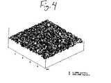
- FIG. 4is an AFM for a transferred SGOI substrate showing surface roughness
- FIGS. 5 - 8are block diagrams of various exemplary embodiments semiconductor structures in accordance with the invention.
- the relaxed SiGe cap layerhas high quality with very low dislocation defect density (less than 1E6/cm 2 ), as the graded buffer accommodates the lattice mismatch between Si and relaxed SiGe. A thin layer of this high quality SiGe will be transferred into the final SGOI structure.
- the surface of the as-grown relaxed SiGe layershows a high roughness around 11 nm to 15 nm due to the underlying strain fields generated by misfit dislocations at the graded layer interfaces and thus chemical-mechanical polishing (CMP) is used to smooth the surface.
- CMPchemical-mechanical polishing
- the donor waferis implanted with hydrogen ion (100 keV, 5E16 H + /cm 2 ) to form a buried hydrogen-rich layer. After a surface clean step in a modified RCA solution, it is bonded to an oxidized 106 Si handle wafer 108 at room temperature as shown in FIG. 1B.
- the wafer bondingis one of the key steps, and the bonding energy should be strong enough in order to sustain the subsequent layer transfer in the next step.
- Good bondingrequires a flat surface and a highly hydrophilic surface before bonding.
- the buried oxide in the final bonded structureis also required to have good electrical properties as it will influence the final device fabricated on it.
- thermal oxide on the donor waferis commonly used before H + implantation and wafer bonding, which becomes the buried oxide in the resulting silicon-on-insulator structure.
- the thermal oxide of the Si donor wafermeets all the requirements, as it has good electrical properties, has flat surface and bonds very well to the handle wafer. Unlike the Si, however, the oxidation of SiGe film results in poor thermal oxide quality, and the Ge segregation during oxidation also degrades the SiGe film. Therefore the thermal oxide of SiGe is not suitable for the SGOI fabrication. In one exemplary experiment the SiGe film will be directly bonded to an oxidized Si handle wafer. The high quality thermal oxide in the handle wafer will become the buried oxide in the final SGOI structure.
- the SiGe waferwent through a clean step.
- one difficulty of SiGe filmis that, SiGe surface becomes rougher during the standard RCA clean, as the NH 4 OH in RCA1 solution etches Ge faster than Si. Rough surface will lead to weak bonding as the contact area is reduced when bonded to the handle wafer.
- H 2 SO 4 —H 2 O 2 solutionis used in the place of RCA1, which also meets the clean process requirement for the subsequent furnace annealing after bonding.
- the SiGe surface after H 2 SO 4 —H 2 O 2 cleanshows better surface roughness compared to RCA1.
- the SiGe waferis dipped in the diluted HF solution to remove the old native oxide. It is then rinsed in DI water thoroughly to make the surface hydrophilic by forming a fresh new native oxide layer that is highly active.
- the SiGe waferis bonded to an oxidized handle wafer at room temperature, and then annealed at 600° C. for 3 hours. During anneal the bonded pair split into two sheets along the buried hydrogen-rich layer, and a thin relaxed Si 0.75 Ge 0.25 film 110 is transferred into the handle wafer, resulting in a SGOI substrate 112 , as shown in FIG. 1B. A final 850° C. anneal improves the Si 0.75 Ge 0.25 /SiO 2 bond. Thereafter, device layers 114 can be processed on the SGOI substrate 112 as shown in FIG. 1C.
- FIGS. 2A and 2Bare infrared transmission images of the as-bonded wafer pair and the final SGOI substrate after splitting, respectively.
- TEMtransmission electron microscopy
- AFMatomic force microscopy
- the TEM cross-section view in FIG. 3shows a ⁇ 640 nm SiGe layer was transferred onto the top of a 550 nm buried oxide (BOX). Surface damage is also shown clearly at the splitting surface with a damage depth of ⁇ 100 nm.
- FIG. 4shows a surface roughness of 11.3 nm in an area of 5 ⁇ 5 ⁇ m 2 by AFM for the as-transferred SGOI.
- the datais similar to those from as-transferred silicon film by smart-cut process, and suggests that a top layer of about 100 nm should be removed by a final CMP step.
- SiGe film transferringonly a thin relaxed SiGe film is removed and the donor wafer can be used again for a donor wafer.
- various device structurescan be realized by growing one or more device layers on the top, as shown in FIG. 2C. Electrical evaluation is in progress by growing a strain Si layer on the top of this SGOI substrate followed by fabrication of strained Si channel devices.
- Bond strengthis important to the process of the invention.
- AFM measurementswere conducted to investigate the SiGe film surface roughness before bonding under different conditions.
- One experimentis designed to investigate how long the SiGe surface should be polished to have smooth surface and good bond strength, since the surface of the as-grown relaxed SiGe layer has a high roughness around 11 nm to 15 nm.
- Several identical 4-inch Si wafers with relaxed Si 0.75 Ge 0.25 filmswere CMPed with optimized polishing conditions for different times.
- the measured surface mircoroughness RMS at an area of 10 ⁇ m ⁇ 10 ⁇ mis 5.5 ⁇ , 4.5 ⁇ and 3.8 ⁇ , for wafer CMPed for 2 min., 4 min. and 6 min. respectively.
- the tested bond strengthincreases with decreasing RMS.
- a CMP time of 6 min.is necessary for good strength.
- the wafer after H 2 SO 4 :H 2 O 2 solutionshows a surface roughness RMS of 2 ⁇ at an area of 1 ⁇ m ⁇ 1 ⁇ m, which after NH 4 OH:H 2 O 2 :H 2 O shows 4.4 ⁇ .
- the conventional RCA cleanroughens the SiGe surface significantly, and H 2 SO 4 :H 2 O 2 should be used for SiGe clean.
- FIG. 5is a block diagram of an exemplary embodiment of a semiconductor structure 500 in accordance with the invention.
- a graded Si 1 ⁇ x Ge x buffer layer 504is grown on a silicon substrate 502 , where the Ge concentration x is increased from zero to a value y in a stepwise manner, and y has a selected value between 0 and 1.
- a second relaxed Si 1 ⁇ y Ge y layer 506is then deposited, and hydrogen ions are implanted into this layer with a selected depth by adjusting implantation energy, forming a buried hydrogen-rich layer 508 .
- the waferis cleaned and bonded to an oxidized handle wafer 510 .
- An anneal treatmentat 500 ⁇ 600° C.
- the standard RCA clean for the silicon surfaceis modified. Since the NH 4 OH in standard RCA1 solution etches Ge faster than Si, the SiGe surface will become rough, leading to a weak bond. A H 2 SO 4 —H 2 O 2 solution is used in the place of RCA1, which also meets the clean process requirement for the subsequent furnace annealing after bonding. The SiGe surface after the H 2 SO 4 —H 2 O 2 clean showed better surface roughness compared to RCA1. After the modified RCA clean, the wafers are then immersed in another fresh H 2 SO 4 —H 2 O 2 solution for 10 to 20 min. H 2 SO 4 —H 2 O 2 renders the SiGe surface hydrophilic. After a rinse in DI wafer and spin drying, the SiGe wafer is bonded to an oxidized handle wafer at room temperature immediately, and then annealed at 500 ⁇ 600° C. for wafer splitting.
- FIG. 6is a block diagram of another exemplary embodiment of a semiconductor structure 600 .
- the structure 600includes a graded Si 1 ⁇ x Ge x buffer layer 604 grown on a silicon substrate 602 , where the Ge concentration x is increased from zero to 1. Then a relaxed pure Ge layer 606 and a III-V material layer 608 , such as a GaAs layer, are epitaxially grown on the Ge layer. Hydrogen ions are implanted into the GaAs layer 608 with a selected depth by adjusting implantation energy, forming a buried hydrogen-rich layer 610 . The wafer is cleaned and bonded to an oxidized handle wafer 612 . An anneal treatment splits the bonded pair at the hydrogen-rich layer 610 . As a result, the upper portion of the GaAs layer 608 remains on the oxidized handle wafer, forming a GaAs-on-insulator substrate.
- FIG. 7.is a block diagram of yet another exemplary embodiment of a semiconductor structure 700 .
- a graded Si 1 ⁇ x Ge x buffer layer 704is grown on a silicon substrate 702 , where the Ge concentration x is increased from zero to a selected value y, where y is less than 0.2.
- a second relaxed Si 1 ⁇ z Ge z layer 706is deposited, where z is between 0.2 to 0.25.
- Hydrogen ionsare implanted into the graded Si 1 ⁇ x Ge x buffer layer 704 with a selected depth, forming a buried hydrogen-rich layer 708 within layer 704 .
- the waferis cleaned and bonded to an oxidized handle wafer 710 .
- An anneal treatment at 500 ⁇ 600 C.°splits the bonded pair at the hydrogen-rich layer 708 .
- the upper portion of the graded Si 1 ⁇ x Ge x buffer layer 704 and the relaxed Si 1 ⁇ z Ge z layer 706remains on the oxidized handle wafer 710 .
- the remaining graded Si 1 ⁇ x Ge x buffer layer 704is then selectively etched by either KOH or TMAH. KOH and TMAH etch Si 1 ⁇ x Ge x fast when x is less 0.2, but becomes very slow when x is larger than 0.2.
- the graded Si 1 ⁇ x Ge x buffer layer 704can be etched selectively, leaving the relaxed Si 1 ⁇ z Ge z layer 706 on the insulating substrate 710 and forming a relaxed SGOI substrate.
- the thickness of the relaxed Si 1 ⁇ z Ge z film 706 on the final SGOI structureis defined by film growth, which is desired in some applications.
- FIG. 8is a block diagram of yet another exemplary embodiment of a semiconductor structure 800 .
- a graded Si 1 ⁇ x Ge x buffer layer 804is grown on a silicon substrate 802 , where the Ge concentration x is increased from zero to a selected value y between 0 and 1.
- a second relaxed Si 1 ⁇ y Ge y layer 806is deposited, followed by a strained Si 1 ⁇ z Ge z layer 808 and another relaxed Si 1 ⁇ y Ge y layer 810 .
- the thickness of layers 806 , 808 , and 810 , and the value zare chosen such that the Si 1 ⁇ z Ge z layer 808 is under equilibrium strain state while the Si 1 ⁇ y Ge y layers 806 and 810 remain relaxed.
- hydrogen ionsmay be introduced into the strained Si 1 ⁇ z Ge z layer 808 , forming a hydrogen-rich layer 812 .
- the waferis cleaned and bonded to an oxidized handle wafer 814 .
- the bonded pairis then separated along the strained Si 1 ⁇ z Ge z layer 808 .
- the crackpropagates along this layer during separation.
- the separationcan be accomplished by a variety of techniques, for example using a mechanical force or an anneal treatment at 500 ⁇ 600 C.° when the hydrogen is also introduced. See, for example, U.S. Pat. Nos. 6,033,974 and 6,184,111, both of which are incorporated herein by reference.
- the relaxed Si 1 ⁇ y Ge y layer 810remains on the oxidized handle wafer, forming a relaxed SGOI substrate.
- the thickness of layers 806 , 808 , and 810 , and the value zmay also be chosen such that there are a good amount of dislocations present in the Si 1 ⁇ z Ge z layer 808 while the top Si 1 ⁇ y Ge y layer 810 remains relaxed and having high quality and limited dislocation defects.
- These dislocation defects in the Si 1 ⁇ z Ge z layer 808can then act as hydrogen trap centers during the subsequent step of introducing ions.
- the hydrogen ionsmay be introduced by various ways, such as ion implantation or ion diffusion or drift by means of electrolytic charging.
- the value of zmay be chosen in such a way that the remaining Si 1 ⁇ z Ge z layer 808 can be etched selectively by KOH or TMAH.
- the layers 806 and 810may also be some other materials, for example pure Ge, or some III-V materials, under the condition that the Ge concentration x in the graded Si 1 ⁇ x Ge x buffer layer 804 is increased from zero to 1.
Landscapes
- Engineering & Computer Science (AREA)
- Physics & Mathematics (AREA)
- Condensed Matter Physics & Semiconductors (AREA)
- General Physics & Mathematics (AREA)
- Manufacturing & Machinery (AREA)
- Computer Hardware Design (AREA)
- Microelectronics & Electronic Packaging (AREA)
- Power Engineering (AREA)
- Chemical & Material Sciences (AREA)
- Materials Engineering (AREA)
- Recrystallisation Techniques (AREA)
- Element Separation (AREA)
Abstract
Description
- This application claims priority from provisional application Ser. No. 60/225,666 filed Aug. 16, 2000.[0001]
- The present invention relates to a production of a general substrate of relaxed Si[0002]1−xGex-on-insulator (SGOI) for various electronics or optoelectronics applications, and the production of monocrystalline III-V or II-VI material-on-insulator substrate.
- Relaxed Si[0003]1−xGex-on-insulator (SGOI) is a very promising technology as it combines the benefits of two advanced technologies: the conventional SOI technology and the disruptive SiGe technology. The SOI configuration offers various advantages associated with the insulating substrate, namely reduced parasitic capacitances, improved isolation, reduced short-channel-effect, etc. High mobility strained-Si, strained-Si1−xGexor strained-Ge MOS devices can be made on SGOI substrates.
- Other III-V optoelectronic devices can also be integrated into the SGOI substrate by matching the lattice constants of III-V materials and the relaxed Si[0004]1−xGex. For example a GaAs layer can be grown on Si1−xGex-on-insulator where x is equal or close to 1. SGOI may serve as an ultimate platform for high speed, low power electronic and optoelectronic applications.
- SGOI has been fabricated by several methods in the prior art. In one method, the separation by implantation of oxygen (SIMOX) technology is used to produce SGOI. High dose oxygen implant was used to bury high concentrations of oxygen in a Si[0005]1−xGexlayer, which was then converted into a buried oxide (BOX) layer upon annealing at high temperature (for example, 1350° C.). See, for example, Mizuno et al. IEEE Electron Device Letters, Vol. 21, No. 5, pp. 230-232, 2000 and Ishilawa et al. Applied Physics Letters, Vol. 75, No. 7, pp. 983-985, 1999. One of the main drawbacks is the quality of the resulting Si1−xGexfilm and BOX. In addition, Ge segregation during high temperature anneal also limits the maximum Ge composition to a low value.
- U.S. Pat. Nos. 5,461,243 and 5,759,898 describe a second method, in which a conventional silicon-on-insulator (SOI) substrate was used as a compliant substrate. In the process, an initially strained Si[0006]1−xGexlayer was deposited on a thin SOI substrate. Upon an anneal treatment, the strain was transferred to the thin silicon film underneath, resulting in relaxation of the top Si1−xGexfilm. The final structure is relaxed-SiGe/strained-Si/insulator, which is not an ideal SGOI structure. The silicon layer in the structure is unnecessary, and may complicate or undermine the performance of devices built on it. For example, it may form a parasitic back channel on this strained-Si, or may confine unwanted electrons due to the band gap offset between the strained-Si and SiGe layer.
- U.S. Pat. Nos. 5,906,951 and 6,059,895 describe the formation of a similar SGOI structure: strained-layer(s)/relaxed-SiGe/Si/insulator structure. The structure was produced by wafer bonding and etch back process using a P[0007]++ layer as an etch stop. The presence of the silicon layer in the above structure may be for the purpose of facilitating Si-insulator wafer bonding, but is unnecessary for ideal SGOI substrates. Again, the silicon layer may also complicate or undermine the performance of devices built on it. For example, it may form a parasitic back channel on this strained-Si, or may confine unwanted electrons due to the band gap offset between the strained-Si and SiGe layer. Moreover, the etch stop of P++ in the above structure is not practical when the first graded Si1−yGeylayer described in the patents has a y value of larger than 0.2. Experiments from research shows Si1−yGeywith y larger than 0.2 is a very good etch stop for both KOH and TMAH, as described in a published PCT application WO 99/53539. Therefore, the KOH will not be able to remove the first graded Si1−yGeylayer and the second relaxed SiGe layer as described in the patents.
- Other attempts include re-crystallization of an amorphous Si[0008]1−xGexlayer deposited on the top of SOI (silicon-on-insulator) substrate, which is again not an ideal SGOI substrate and the silicon layer is unnecessary, and may complicate or undermine the performance of devices built on it. Note Yeo et al. IEEE Electron Device Letters, Vol. 21, No. 4, pp. 161-163, 2000. The relaxation of the resultant SiGe film and quality of the resulting structure are main concerns.
- From the above, there is a need for a simple technique for relaxed SGOI substrate production, a need for a technique for production of high quality SGOI and other III-V material-on-insulator, and a need for a technique for wide range of material transfer.[0009]
- According to the invention, there is provided an improved technique for production of wide range of high quality material is provided. In particular, the production of relaxed Si[0010]1−xGex-on-insulator (SGOI) substrate or relaxed III-V or II-VI material-on-insulator, such as GaAs-on-insulator, is described. High quality monocrystalline relaxed SiGe layer, relaxed Ge layer, or other relaxed III-V material layer is grown on a silicon substrate using a graded Si1−xGexepitaxial growth technique. A thin film of the layer is transferred into an oxidized handle wafer by wafer bonding and wafer splitting using hydrogen ion implantation. The invention makes use of the graded Si1−xGexbuffer structure, resulting in a simplified and improved process.
- The invention also provides a method allowing a wide range of device materials to be integrated into the inexpensive silicon substrate. For example, it allows production of Si[0011]1−xGex-on-insulator with wide range of Ge concentration, and allows production of many III-V or II-VI materials on insulator like GaAs, AlAs, ZnSe and InGaP. The use of graded Si1−xGexbuffer in the invention allows high quality materials with limited dislocation defects to be produced and transferred. In one example, SGOI is produced using a SiGe structure in which a region in the graded buffer can act as a natural etch stop.
- The invention provides a process and method for producing monocrystalline semiconductor layers. In an exemplary embodiment, a graded Si[0012]1−xGex(x increases from 0 to y) is deposited on a first silicon substrate, followed by deposition of a relaxed Si1−yGeylayer, a thin strained Si1−zGezlayer and another relaxed Si1−yGeylayer. Hydrogen ions are then introduced into the strained SizGezlayer. The relaxed Si1−yGeylayer is bonded to a second oxidized substrate. An annealing treatment splits the bonded pair at the strained Si layer, whereby the second relaxed Si1−yGeylayer remains on said second substrate.
- In another exemplary embodiment, a graded Si[0013]1−xGexis deposited on a first silicon substrate, where the Ge concentration x is increased from 0 to 1. Then a relaxed GaAs layer is deposited on the relaxed Ge buffer. As the lattice constant of GaAs is close to that of Ge, GaAs has high quality with limited dislocation defects. Hydrogen ions are introduced into the relaxed GaAs layer at the selected depth. The relaxed GaAs layer is bonded to a second oxidized substrate. An annealing treatment splits the bonded pair at the hydrogen ion rich layer, whereby the upper portion of relaxed GaAs layer remains on said second substrate.
- FIGS.[0014]1A-1C are block diagrams showing the process of producing a SGOI substrate in accordance with the invention;
- FIGS. 2A and 2B are infrared transmission images of an as-bonded wafer pair and a final SGOI substrate after splitting, respectively;[0015]
- FIG. 3 is a TEM cross-section view of a SiGe layer that was transferred onto the top of a buried oxide;[0016]
- FIG. 4 is an AFM for a transferred SGOI substrate showing surface roughness; and[0017]
- FIGS.[0018]5-8 are block diagrams of various exemplary embodiments semiconductor structures in accordance with the invention.
- An example of a process in which SGOI is created by layer transfer is described. The experiment was performed in two stages. In the first stage, heteroepitaxial SiGe layers are formed by a graded epitaxial growth technology. Starting with a 4-inch Si ([0019]100)
donor wafer 100, a linearly stepwise compositionally graded Si1−xGexbuffer102 is deposited with CVD, by increasing Ge concentration from zero to 25%. Then a 2.5 μm relaxed Si0.75Ge0.25cap layer104 is deposited with the final Ge composition, as shown in FIG. 1A. - The relaxed SiGe cap layer has high quality with very low dislocation defect density (less than 1E6/cm[0020]2), as the graded buffer accommodates the lattice mismatch between Si and relaxed SiGe. A thin layer of this high quality SiGe will be transferred into the final SGOI structure. The surface of the as-grown relaxed SiGe layer shows a high roughness around 11 nm to 15 nm due to the underlying strain fields generated by misfit dislocations at the graded layer interfaces and thus chemical-mechanical polishing (CMP) is used to smooth the surface. In the second stage, the donor wafer is implanted with hydrogen ion (100 keV, 5E16 H+/cm2) to form a buried hydrogen-rich layer. After a surface clean step in a modified RCA solution, it is bonded to an oxidized106
Si handle wafer 108 at room temperature as shown in FIG. 1B. - The wafer bonding is one of the key steps, and the bonding energy should be strong enough in order to sustain the subsequent layer transfer in the next step. Good bonding requires a flat surface and a highly hydrophilic surface before bonding. On the other hand, the buried oxide in the final bonded structure is also required to have good electrical properties as it will influence the final device fabricated on it. In the conventional Si film transfer, thermal oxide on the donor wafer is commonly used before H[0021]+ implantation and wafer bonding, which becomes the buried oxide in the resulting silicon-on-insulator structure.
- The thermal oxide of the Si donor wafer meets all the requirements, as it has good electrical properties, has flat surface and bonds very well to the handle wafer. Unlike the Si, however, the oxidation of SiGe film results in poor thermal oxide quality, and the Ge segregation during oxidation also degrades the SiGe film. Therefore the thermal oxide of SiGe is not suitable for the SGOI fabrication. In one exemplary experiment the SiGe film will be directly bonded to an oxidized Si handle wafer. The high quality thermal oxide in the handle wafer will become the buried oxide in the final SGOI structure.[0022]
- Having a flat surface after a CMP step, the SiGe wafer went through a clean step. Compared to Si, one difficulty of SiGe film is that, SiGe surface becomes rougher during the standard RCA clean, as the NH[0023]4OH in RCA1 solution etches Ge faster than Si. Rough surface will lead to weak bonding as the contact area is reduced when bonded to the handle wafer. In this exemplary embodiment, H2SO4—H2O2solution is used in the place of RCA1, which also meets the clean process requirement for the subsequent furnace annealing after bonding. The SiGe surface after H2SO4—H2O2clean shows better surface roughness compared to RCA1.
- After this modified clean procedure, the SiGe wafer is dipped in the diluted HF solution to remove the old native oxide. It is then rinsed in DI water thoroughly to make the surface hydrophilic by forming a fresh new native oxide layer that is highly active. After spinning dry, the SiGe wafer is bonded to an oxidized handle wafer at room temperature, and then annealed at 600° C. for 3 hours. During anneal the bonded pair split into two sheets along the buried hydrogen-rich layer, and a thin relaxed Si[0024]0.75Ge0.25film110 is transferred into the handle wafer, resulting in a
SGOI substrate 112, as shown in FIG. 1B. A final 850° C. anneal improves the Si0.75Ge0.25/SiO2bond. Thereafter, device layers114 can be processed on theSGOI substrate 112 as shown in FIG. 1C. - FIGS. 2A and 2B are infrared transmission images of the as-bonded wafer pair and the final SGOI substrate after splitting, respectively. To investigate the surface of the as-transferred SGOI substrate, transmission electron microscopy (TEM) and atomic force microscopy (AFM) were used. The TEM cross-section view in FIG. 3 shows a ˜640 nm SiGe layer was transferred onto the top of a 550 nm buried oxide (BOX). Surface damage is also shown clearly at the splitting surface with a damage depth of ˜100 nm.[0025]
- FIG. 4 shows a surface roughness of 11.3 nm in an area of 5×5 μm[0026]2by AFM for the as-transferred SGOI. The data is similar to those from as-transferred silicon film by smart-cut process, and suggests that a top layer of about 100 nm should be removed by a final CMP step. After SiGe film transferring, only a thin relaxed SiGe film is removed and the donor wafer can be used again for a donor wafer. Starting from this general SGOI substrate, various device structures can be realized by growing one or more device layers on the top, as shown in FIG. 2C. Electrical evaluation is in progress by growing a strain Si layer on the top of this SGOI substrate followed by fabrication of strained Si channel devices.
- Bond strength is important to the process of the invention. AFM measurements were conducted to investigate the SiGe film surface roughness before bonding under different conditions. One experiment is designed to investigate how long the SiGe surface should be polished to have smooth surface and good bond strength, since the surface of the as-grown relaxed SiGe layer has a high roughness around 11 nm to 15 nm. Several identical 4-inch Si wafers with relaxed Si[0027]0.75Ge0.25films were CMPed with optimized polishing conditions for different times. Using AFM, the measured surface mircoroughness RMS at an area of 10 μm×10 μm is 5.5 Å, 4.5 Å and 3.8 Å, for wafer CMPed for 2 min., 4 min. and 6 min. respectively. After bonding to identical handle wafers, the tested bond strength increases with decreasing RMS. A CMP time of 6 min. is necessary for good strength.
- In another experiment, two identical 4-inch Si wafers with relaxed Si[0028]0.75Ge0.25films were CMPed for 8 min. After two cleaning steps in H2SO4:H2O2solution and one step in diluted HF solution, one wafer was put in a new H2SO4:H2O2(3:1) solution and another in a new NH4OH:H2O2:H2O (1:1:5), i.e. the conventional RCA1 solution, both for 15 min. The resultant wafers were tested using AFM. The wafer after H2SO4:H2O2solution shows a surface roughness RMS of 2 Å at an area of 1 μm×1 μm, which after NH4OH:H2O2:H2O shows 4.4 Å. Clearly, the conventional RCA clean roughens the SiGe surface significantly, and H2SO4:H2O2should be used for SiGe clean.
- In yet another experiment, the clean procedure is optimized before bonding. For direct SiGe wafer to oxidized handle wafer bonding (SiGe-oxide bonding), several different clean procedures were tested. It has been found that the H[0029]2SO4:H2O2(2˜4:1) solution followed by DI water rinse and spin dry gives good bond strength. Alternatively, one can also deposit an oxide layer on the SiGe wafer and then CMP the oxide layer. In this case SiGe/oxide is bonded to an oxidized handle wafer, i.e. oxide-oxide bonding. Among different clean procedures, it was found that NH4OH:H2O2:H2O clean and DI water rinse following by diluted HF, DI water rinse and spin dry gives very good bond strength.
- FIG. 5 is a block diagram of an exemplary embodiment of a[0030]
semiconductor structure 500 in accordance with the invention. A graded Si1−xGexbuffer layer504 is grown on asilicon substrate 502, where the Ge concentration x is increased from zero to a value y in a stepwise manner, and y has a selected value between 0 and 1. A second relaxed Si1−yGeylayer506 is then deposited, and hydrogen ions are implanted into this layer with a selected depth by adjusting implantation energy, forming a buried hydrogen-rich layer508. The wafer is cleaned and bonded to an oxidizedhandle wafer 510. An anneal treatment at 500˜600° C. splits the bonded pair at the hydrogen-rich layer508. As a result, the upper portion of the relaxed Si1−yGeylayer506 remains on the oxidized handle wafer, forming a SGOI substrate. The above description also includes production of Ge-on-insulator where y=1. - During the wafer clean step prior to bonding, the standard RCA clean for the silicon surface is modified. Since the NH[0031]4OH in standard RCA1 solution etches Ge faster than Si, the SiGe surface will become rough, leading to a weak bond. A H2SO4—H2O2solution is used in the place of RCA1, which also meets the clean process requirement for the subsequent furnace annealing after bonding. The SiGe surface after the H2SO4—H2O2clean showed better surface roughness compared to RCA1. After the modified RCA clean, the wafers are then immersed in another fresh H2SO4—H2O2solution for 10 to 20 min. H2SO4—H2O2renders the SiGe surface hydrophilic. After a rinse in DI wafer and spin drying, the SiGe wafer is bonded to an oxidized handle wafer at room temperature immediately, and then annealed at 500˜600° C. for wafer splitting.
- FIG. 6 is a block diagram of another exemplary embodiment of a[0032]
semiconductor structure 600. Thestructure 600 includes a graded Si1−xGexbuffer layer604 grown on asilicon substrate 602, where the Ge concentration x is increased from zero to 1. Then a relaxedpure Ge layer 606 and a III-V material layer 608, such as a GaAs layer, are epitaxially grown on the Ge layer. Hydrogen ions are implanted into theGaAs layer 608 with a selected depth by adjusting implantation energy, forming a buried hydrogen-rich layer 610. The wafer is cleaned and bonded to an oxidizedhandle wafer 612. An anneal treatment splits the bonded pair at the hydrogen-rich layer 610. As a result, the upper portion of theGaAs layer 608 remains on the oxidized handle wafer, forming a GaAs-on-insulator substrate. - FIG. 7. is a block diagram of yet another exemplary embodiment of a[0033]
semiconductor structure 700. A graded Si1−xGexbuffer layer704 is grown on asilicon substrate 702, where the Ge concentration x is increased from zero to a selected value y, where y is less than 0.2. A second relaxed Si1−zGezlayer706 is deposited, where z is between 0.2 to 0.25. Hydrogen ions are implanted into the graded Si1−xGexbuffer layer704 with a selected depth, forming a buried hydrogen-rich layer 708 withinlayer 704. The wafer is cleaned and bonded to an oxidizedhandle wafer 710. An anneal treatment at 500˜600 C.° splits the bonded pair at the hydrogen-rich layer 708. - As a result, the upper portion of the graded Si[0034]1−xGexbuffer layer704 and the relaxed Si1−zGezlayer706 remains on the oxidized
handle wafer 710. The remaining graded Si1−xGexbuffer layer704 is then selectively etched by either KOH or TMAH. KOH and TMAH etch Si1−xGexfast when x is less 0.2, but becomes very slow when x is larger than 0.2. Thus, the graded Si1−xGexbuffer layer704 can be etched selectively, leaving the relaxed Si1−zGezlayer706 on the insulatingsubstrate 710 and forming a relaxed SGOI substrate. In this process, the thickness of the relaxed Si1−zGezfilm706 on the final SGOI structure is defined by film growth, which is desired in some applications. - FIG. 8 is a block diagram of yet another exemplary embodiment of a[0035]
semiconductor structure 800. A graded Si1−xGexbuffer layer804 is grown on asilicon substrate 802, where the Ge concentration x is increased from zero to a selected value y between 0 and 1. A second relaxed Si1−yGeylayer806 is deposited, followed by a strained Si1−zGezlayer808 and another relaxed Si1−yGeylayer810. The thickness oflayers rich layer 812. The wafer is cleaned and bonded to an oxidizedhandle wafer 814. The bonded pair is then separated along the strained Si1−zGezlayer808. - Since the strain makes the layer weaker, the crack propagates along this layer during separation. The separation can be accomplished by a variety of techniques, for example using a mechanical force or an anneal treatment at 500˜600 C.° when the hydrogen is also introduced. See, for example, U.S. Pat. Nos. 6,033,974 and 6,184,111, both of which are incorporated herein by reference. As a result, the relaxed Si[0036]1−yGeylayer810 remains on the oxidized handle wafer, forming a relaxed SGOI substrate. The thickness of
layers - These dislocation defects in the Si[0037]1−zGezlayer808 can then act as hydrogen trap centers during the subsequent step of introducing ions. The hydrogen ions may be introduced by various ways, such as ion implantation or ion diffusion or drift by means of electrolytic charging. The value of z may be chosen in such a way that the remaining Si1−zGezlayer808 can be etched selectively by KOH or TMAH. The
layers - After all the semiconductor-on-insulator substrate obtained by the approaches described above, various device layers can be further grown on the top. Before the regrowth, CMP maybe used to polish the surface.[0038]
- Although the present invention has been shown and described with respect to several preferred embodiments thereof, various changes, omissions and additions to the form and detail thereof, may be made therein, without departing from the spirit and scope of the invention.[0039]
Claims (55)
Priority Applications (2)
| Application Number | Priority Date | Filing Date | Title |
|---|---|---|---|
| US10/384,160US6737670B2 (en) | 2000-08-16 | 2003-03-07 | Semiconductor substrate structure |
| US10/802,185US6921914B2 (en) | 2000-08-16 | 2004-03-17 | Process for producing semiconductor article using graded epitaxial growth |
Applications Claiming Priority (3)
| Application Number | Priority Date | Filing Date | Title |
|---|---|---|---|
| US22566600P | 2000-08-16 | 2000-08-16 | |
| US09/928,126US6573126B2 (en) | 2000-08-16 | 2001-08-10 | Process for producing semiconductor article using graded epitaxial growth |
| US10/384,160US6737670B2 (en) | 2000-08-16 | 2003-03-07 | Semiconductor substrate structure |
Related Parent Applications (1)
| Application Number | Title | Priority Date | Filing Date |
|---|---|---|---|
| US09/928,126DivisionUS6573126B2 (en) | 2000-08-16 | 2001-08-10 | Process for producing semiconductor article using graded epitaxial growth |
Related Child Applications (1)
| Application Number | Title | Priority Date | Filing Date |
|---|---|---|---|
| US10/802,185ContinuationUS6921914B2 (en) | 2000-08-16 | 2004-03-17 | Process for producing semiconductor article using graded epitaxial growth |
Publications (2)
| Publication Number | Publication Date |
|---|---|
| US20030168654A1true US20030168654A1 (en) | 2003-09-11 |
| US6737670B2 US6737670B2 (en) | 2004-05-18 |
Family
ID=22845751
Family Applications (5)
| Application Number | Title | Priority Date | Filing Date |
|---|---|---|---|
| US09/928,126Expired - LifetimeUS6573126B2 (en) | 2000-08-16 | 2001-08-10 | Process for producing semiconductor article using graded epitaxial growth |
| US10/379,355Expired - LifetimeUS6713326B2 (en) | 2000-08-16 | 2003-03-04 | Process for producing semiconductor article using graded epitaxial growth |
| US10/384,160Expired - Fee RelatedUS6737670B2 (en) | 2000-08-16 | 2003-03-07 | Semiconductor substrate structure |
| US10/802,185Expired - LifetimeUS6921914B2 (en) | 2000-08-16 | 2004-03-17 | Process for producing semiconductor article using graded epitaxial growth |
| US10/802,186AbandonedUS20050009288A1 (en) | 2000-08-16 | 2004-03-17 | Process for producing semiconductor article using graded epitaxial growth |
Family Applications Before (2)
| Application Number | Title | Priority Date | Filing Date |
|---|---|---|---|
| US09/928,126Expired - LifetimeUS6573126B2 (en) | 2000-08-16 | 2001-08-10 | Process for producing semiconductor article using graded epitaxial growth |
| US10/379,355Expired - LifetimeUS6713326B2 (en) | 2000-08-16 | 2003-03-04 | Process for producing semiconductor article using graded epitaxial growth |
Family Applications After (2)
| Application Number | Title | Priority Date | Filing Date |
|---|---|---|---|
| US10/802,185Expired - LifetimeUS6921914B2 (en) | 2000-08-16 | 2004-03-17 | Process for producing semiconductor article using graded epitaxial growth |
| US10/802,186AbandonedUS20050009288A1 (en) | 2000-08-16 | 2004-03-17 | Process for producing semiconductor article using graded epitaxial growth |
Country Status (5)
| Country | Link |
|---|---|
| US (5) | US6573126B2 (en) |
| EP (1) | EP1309989B1 (en) |
| JP (2) | JP2004507084A (en) |
| DE (1) | DE60125952T2 (en) |
| WO (1) | WO2002015244A2 (en) |
Cited By (11)
| Publication number | Priority date | Publication date | Assignee | Title |
|---|---|---|---|---|
| US20040192067A1 (en)* | 2003-02-28 | 2004-09-30 | Bruno Ghyselen | Method for forming a relaxed or pseudo-relaxed useful layer on a substrate |
| US20050070070A1 (en)* | 2003-09-29 | 2005-03-31 | International Business Machines | Method of forming strained silicon on insulator |
| US20050070078A1 (en)* | 2003-09-30 | 2005-03-31 | Nicolas Daval | Indirect bonding with disappearance of bonding layer |
| US6921914B2 (en) | 2000-08-16 | 2005-07-26 | Massachusetts Institute Of Technology | Process for producing semiconductor article using graded epitaxial growth |
| US20050250294A1 (en)* | 2003-02-28 | 2005-11-10 | Bruno Ghyselen | Method for forming a relaxed or pseudo-relaxed useful layer on a substrate |
| US7018909B2 (en) | 2003-02-28 | 2006-03-28 | S.O.I.Tec Silicon On Insulator Technologies S.A. | Forming structures that include a relaxed or pseudo-relaxed layer on a substrate |
| US20060175608A1 (en)* | 2005-02-09 | 2006-08-10 | Celler George K | Relaxation of a strained layer using a molten layer |
| US20070023066A1 (en)* | 2003-09-10 | 2007-02-01 | Isao Yokokawa | Multilayer substrate cleaning method, substrate bonding method, and bonded wafer manufacturing method |
| US20080075980A1 (en)* | 2006-09-25 | 2008-03-27 | Seagate Technology Llc | Epitaxial ferroelectric and magnetic recording structures including graded lattice matching layers |
| US20080108194A1 (en)* | 2005-08-31 | 2008-05-08 | Szu-Yu Wang | Memory device and manufacturing method thereof |
| US9496140B2 (en) | 2009-07-31 | 2016-11-15 | Globalfoundries Inc. | Silicon wafer based structure for heterostructure solar cells |
Families Citing this family (195)
| Publication number | Priority date | Publication date | Assignee | Title |
|---|---|---|---|---|
| JP3535527B2 (en)* | 1997-06-24 | 2004-06-07 | マサチューセッツ インスティテュート オブ テクノロジー | Controlling threading dislocations in germanium-on-silicon using graded GeSi layer and planarization |
| US7227176B2 (en)* | 1998-04-10 | 2007-06-05 | Massachusetts Institute Of Technology | Etch stop layer system |
| US6633066B1 (en)* | 2000-01-07 | 2003-10-14 | Samsung Electronics Co., Ltd. | CMOS integrated circuit devices and substrates having unstrained silicon active layers |
| JP2003520444A (en) | 2000-01-20 | 2003-07-02 | アンバーウェーブ システムズ コーポレイション | Low threading dislocation density lattice-mismatched epilayer that does not require high-temperature growth |
| US6750130B1 (en) | 2000-01-20 | 2004-06-15 | Amberwave Systems Corporation | Heterointegration of materials using deposition and bonding |
| US6602613B1 (en) | 2000-01-20 | 2003-08-05 | Amberwave Systems Corporation | Heterointegration of materials using deposition and bonding |
| AU2001263211A1 (en) | 2000-05-26 | 2001-12-11 | Amberwave Systems Corporation | Buried channel strained silicon fet using an ion implanted doped layer |
| US6890835B1 (en)* | 2000-10-19 | 2005-05-10 | International Business Machines Corporation | Layer transfer of low defect SiGe using an etch-back process |
| US6649480B2 (en)* | 2000-12-04 | 2003-11-18 | Amberwave Systems Corporation | Method of fabricating CMOS inverter and integrated circuits utilizing strained silicon surface channel MOSFETs |
| US20020100942A1 (en)* | 2000-12-04 | 2002-08-01 | Fitzgerald Eugene A. | CMOS inverter and integrated circuits utilizing strained silicon surface channel MOSFETs |
| US6703688B1 (en) | 2001-03-02 | 2004-03-09 | Amberwave Systems Corporation | Relaxed silicon germanium platform for high speed CMOS electronics and high speed analog circuits |
| US6723661B2 (en)* | 2001-03-02 | 2004-04-20 | Amberwave Systems Corporation | Relaxed silicon germanium platform for high speed CMOS electronics and high speed analog circuits |
| US6830976B2 (en) | 2001-03-02 | 2004-12-14 | Amberwave Systems Corproation | Relaxed silicon germanium platform for high speed CMOS electronics and high speed analog circuits |
| US6724008B2 (en) | 2001-03-02 | 2004-04-20 | Amberwave Systems Corporation | Relaxed silicon germanium platform for high speed CMOS electronics and high speed analog circuits |
| WO2002082514A1 (en) | 2001-04-04 | 2002-10-17 | Massachusetts Institute Of Technology | A method for semiconductor device fabrication |
| US20050026432A1 (en)* | 2001-04-17 | 2005-02-03 | Atwater Harry A. | Wafer bonded epitaxial templates for silicon heterostructures |
| AU2002322105A1 (en) | 2001-06-14 | 2003-01-02 | Amberware Systems Corporation | Method of selective removal of sige alloys |
| US7301180B2 (en) | 2001-06-18 | 2007-11-27 | Massachusetts Institute Of Technology | Structure and method for a high-speed semiconductor device having a Ge channel layer |
| WO2003001671A2 (en) | 2001-06-21 | 2003-01-03 | Amberwave Systems Corporation | Improved enhancement of p-type metal-oxide-semiconductor field-effect transistors |
| EP1415331A2 (en)* | 2001-08-06 | 2004-05-06 | Massachusetts Institute Of Technology | Formation of planar strained layers |
| US6974735B2 (en) | 2001-08-09 | 2005-12-13 | Amberwave Systems Corporation | Dual layer Semiconductor Devices |
| US7138649B2 (en)* | 2001-08-09 | 2006-11-21 | Amberwave Systems Corporation | Dual-channel CMOS transistors with differentially strained channels |
| US6831292B2 (en)* | 2001-09-21 | 2004-12-14 | Amberwave Systems Corporation | Semiconductor structures employing strained material layers with defined impurity gradients and methods for fabricating same |
| US6933518B2 (en)* | 2001-09-24 | 2005-08-23 | Amberwave Systems Corporation | RF circuits including transistors having strained material layers |
| JP2003205336A (en)* | 2002-01-08 | 2003-07-22 | Tori Techno:Kk | High strength stainless steel bolt and manufacturing method therefor |
| US6805962B2 (en)* | 2002-01-23 | 2004-10-19 | International Business Machines Corporation | Method of creating high-quality relaxed SiGe-on-insulator for strained Si CMOS applications |
| US6746902B2 (en)* | 2002-01-31 | 2004-06-08 | Sharp Laboratories Of America, Inc. | Method to form relaxed sige layer with high ge content |
| US6649492B2 (en)* | 2002-02-11 | 2003-11-18 | International Business Machines Corporation | Strained Si based layer made by UHV-CVD, and devices therein |
| US6793731B2 (en)* | 2002-03-13 | 2004-09-21 | Sharp Laboratories Of America, Inc. | Method for recrystallizing an amorphized silicon germanium film overlying silicon |
| WO2003079415A2 (en) | 2002-03-14 | 2003-09-25 | Amberwave Systems Corporation | Methods for fabricating strained layers on semiconductor substrates |
| US7132348B2 (en)* | 2002-03-25 | 2006-11-07 | Micron Technology, Inc. | Low k interconnect dielectric using surface transformation |
| GB0209737D0 (en)* | 2002-04-29 | 2002-06-05 | Univ Newcastle | Method of isolating adjacent components of a semiconductor device |
| US7307273B2 (en) | 2002-06-07 | 2007-12-11 | Amberwave Systems Corporation | Control of strain in device layers by selective relaxation |
| AU2003238963A1 (en) | 2002-06-07 | 2003-12-22 | Amberwave Systems Corporation | Semiconductor devices having strained dual channel layers |
| US20030227057A1 (en) | 2002-06-07 | 2003-12-11 | Lochtefeld Anthony J. | Strained-semiconductor-on-insulator device structures |
| US6995430B2 (en) | 2002-06-07 | 2006-02-07 | Amberwave Systems Corporation | Strained-semiconductor-on-insulator device structures |
| US7335545B2 (en) | 2002-06-07 | 2008-02-26 | Amberwave Systems Corporation | Control of strain in device layers by prevention of relaxation |
| WO2003105189A2 (en)* | 2002-06-07 | 2003-12-18 | Amberwave Systems Corporation | Strained-semiconductor-on-insulator device structures |
| US7074623B2 (en) | 2002-06-07 | 2006-07-11 | Amberwave Systems Corporation | Methods of forming strained-semiconductor-on-insulator finFET device structures |
| US7615829B2 (en) | 2002-06-07 | 2009-11-10 | Amberwave Systems Corporation | Elevated source and drain elements for strained-channel heterojuntion field-effect transistors |
| US6946371B2 (en) | 2002-06-10 | 2005-09-20 | Amberwave Systems Corporation | Methods of fabricating semiconductor structures having epitaxially grown source and drain elements |
| US6982474B2 (en) | 2002-06-25 | 2006-01-03 | Amberwave Systems Corporation | Reacted conductive gate electrodes |
| US7157119B2 (en) | 2002-06-25 | 2007-01-02 | Ppg Industries Ohio, Inc. | Method and compositions for applying multiple overlying organic pigmented decorations on ceramic substrates |
| US6953736B2 (en) | 2002-07-09 | 2005-10-11 | S.O.I.Tec Silicon On Insulator Technologies S.A. | Process for transferring a layer of strained semiconductor material |
| FR2842350B1 (en)* | 2002-07-09 | 2005-05-13 | METHOD FOR TRANSFERRING A LAYER OF CONCEALED SEMICONDUCTOR MATERIAL | |
| US7510949B2 (en) | 2002-07-09 | 2009-03-31 | S.O.I.Tec Silicon On Insulator Technologies | Methods for producing a multilayer semiconductor structure |
| FR2842349B1 (en) | 2002-07-09 | 2005-02-18 | TRANSFERRING A THIN LAYER FROM A PLATE COMPRISING A BUFFER LAYER | |
| FR2848334A1 (en)* | 2002-12-06 | 2004-06-11 | Soitec Silicon On Insulator | Multi-layer structure production of semiconductor materials with different mesh parameters comprises epitaxy of thin film on support substrate and adhesion on target substrate |
| US7018910B2 (en) | 2002-07-09 | 2006-03-28 | S.O.I.Tec Silicon On Insulator Technologies S.A. | Transfer of a thin layer from a wafer comprising a buffer layer |
| US6841457B2 (en)* | 2002-07-16 | 2005-01-11 | International Business Machines Corporation | Use of hydrogen implantation to improve material properties of silicon-germanium-on-insulator material made by thermal diffusion |
| AU2003274922A1 (en) | 2002-08-23 | 2004-03-11 | Amberwave Systems Corporation | Semiconductor heterostructures having reduced dislocation pile-ups and related methods |
| JP2005537685A (en)* | 2002-08-26 | 2005-12-08 | エス.オー.アイ.テック、シリコン、オン、インシュレター、テクノロジーズ | Mechanical recycling of the wafer after removing the layer from the wafer containing the buffer layer |
| US7008857B2 (en)* | 2002-08-26 | 2006-03-07 | S.O.I.Tec Silicon On Insulator Technologies S.A. | Recycling a wafer comprising a buffer layer, after having separated a thin layer therefrom |
| FR2843826B1 (en)* | 2002-08-26 | 2006-12-22 | RECYCLING A PLATE COMPRISING A BUFFER LAYER AFTER SELECTING A THIN LAYER | |
| FR2843827B1 (en)* | 2002-08-26 | 2005-05-27 | MECHANICAL RECYCLING OF A PLATE COMPRISING A STAMP LAYER AFTER SELECTING A THIN LAYER | |
| KR100931421B1 (en)* | 2002-08-26 | 2009-12-11 | 에스. 오. 이. 떼끄 씰리꽁 오 냉쉴라또흐 떼끄놀로지 | Recycling a wafer comprising a buffer layer, after having taken off a thin layer therefrom |
| US7594967B2 (en)* | 2002-08-30 | 2009-09-29 | Amberwave Systems Corporation | Reduction of dislocation pile-up formation during relaxed lattice-mismatched epitaxy |
| FR2844634B1 (en)* | 2002-09-18 | 2005-05-27 | Soitec Silicon On Insulator | FORMATION OF A RELAXED USEFUL LAYER FROM A PLATE WITHOUT BUFFER LAYER |
| US20090325362A1 (en)* | 2003-01-07 | 2009-12-31 | Nabil Chhaimi | Method of recycling an epitaxied donor wafer |
| CN100483666C (en)* | 2003-01-07 | 2009-04-29 | S.O.I.Tec绝缘体上硅技术公司 | Recycling of a wafer comprising a multi-layer structure after taking-off a thin layer |
| KR100874788B1 (en)* | 2003-01-07 | 2008-12-18 | 에스. 오. 이. 떼끄 씰리꽁 오 냉쉴라또흐 떼끄놀로지 | Recycling method by mechanical means of a wafer including a peeling structure after thin layer peeling |
| EP1439570A1 (en) | 2003-01-14 | 2004-07-21 | Interuniversitair Microelektronica Centrum ( Imec) | SiGe strain relaxed buffer for high mobility devices and a method of fabricating it |
| JP4659732B2 (en)* | 2003-01-27 | 2011-03-30 | 台湾積體電路製造股▲ふん▼有限公司 | Method for forming a semiconductor layer |
| EP1443550A1 (en)* | 2003-01-29 | 2004-08-04 | S.O.I. Tec Silicon on Insulator Technologies S.A. | A method for fabricating a strained crystalline layer on an insulator, a semiconductor structure therefor, and a fabricated semiconductor structure |
| US6995427B2 (en) | 2003-01-29 | 2006-02-07 | S.O.I.Tec Silicon On Insulator Technologies S.A. | Semiconductor structure for providing strained crystalline layer on insulator and method for fabricating same |
| US7399681B2 (en)* | 2003-02-18 | 2008-07-15 | Corning Incorporated | Glass-based SOI structures |
| US7176528B2 (en)* | 2003-02-18 | 2007-02-13 | Corning Incorporated | Glass-based SOI structures |
| FR2851848B1 (en)* | 2003-02-28 | 2005-07-08 | Soitec Silicon On Insulator | RELAXATION AT HIGH TEMPERATURE OF A THIN LAYER AFTER TRANSFER |
| WO2004081982A2 (en) | 2003-03-07 | 2004-09-23 | Amberwave Systems Corporation | Shallow trench isolation process |
| DE10310740A1 (en)* | 2003-03-10 | 2004-09-30 | Forschungszentrum Jülich GmbH | Method for producing a stress-relaxed layer structure on a non-lattice-matched substrate, and use of such a layer system in electronic and / or optoelectronic components |
| US7682947B2 (en)* | 2003-03-13 | 2010-03-23 | Asm America, Inc. | Epitaxial semiconductor deposition methods and structures |
| US7238595B2 (en)* | 2003-03-13 | 2007-07-03 | Asm America, Inc. | Epitaxial semiconductor deposition methods and structures |
| DE10318284A1 (en)* | 2003-04-22 | 2004-11-25 | Forschungszentrum Jülich GmbH | Process for producing a strained layer on a substrate and layer structure |
| JP4532846B2 (en)* | 2003-05-07 | 2010-08-25 | キヤノン株式会社 | Manufacturing method of semiconductor substrate |
| US20050124137A1 (en)* | 2003-05-07 | 2005-06-09 | Canon Kabushiki Kaisha | Semiconductor substrate and manufacturing method therefor |
| US7662701B2 (en)* | 2003-05-21 | 2010-02-16 | Micron Technology, Inc. | Gettering of silicon on insulator using relaxed silicon germanium epitaxial proximity layers |
| US7501329B2 (en)* | 2003-05-21 | 2009-03-10 | Micron Technology, Inc. | Wafer gettering using relaxed silicon germanium epitaxial proximity layers |
| ATE504082T1 (en)* | 2003-05-27 | 2011-04-15 | Soitec Silicon On Insulator | METHOD FOR PRODUCING A HETEROEPITACTIC MICROSTRUCTURE |
| US7049660B2 (en)* | 2003-05-30 | 2006-05-23 | International Business Machines Corporation | High-quality SGOI by oxidation near the alloy melting temperature |
| US7045401B2 (en)* | 2003-06-23 | 2006-05-16 | Sharp Laboratories Of America, Inc. | Strained silicon finFET device |
| FR2857953B1 (en)* | 2003-07-21 | 2006-01-13 | Commissariat Energie Atomique | STACKED STRUCTURE, AND METHOD FOR MANUFACTURING THE SAME |
| US20050233548A1 (en)* | 2003-07-23 | 2005-10-20 | Kazuhisa Arai | Method for fabricating semiconductor wafer |
| FR2857983B1 (en)* | 2003-07-24 | 2005-09-02 | Soitec Silicon On Insulator | PROCESS FOR PRODUCING AN EPITAXIC LAYER |
| US7538010B2 (en)* | 2003-07-24 | 2009-05-26 | S.O.I.Tec Silicon On Insulator Technologies | Method of fabricating an epitaxially grown layer |
| KR20060039915A (en)* | 2003-07-30 | 2006-05-09 | 에이에스엠 아메리카, 인코포레이티드 | Epitaxial Growth of a Relaxed Silicon Germanium Layer |
| US7153753B2 (en)* | 2003-08-05 | 2006-12-26 | Micron Technology, Inc. | Strained Si/SiGe/SOI islands and processes of making same |
| US20050081910A1 (en)* | 2003-08-22 | 2005-04-21 | Danielson David T. | High efficiency tandem solar cells on silicon substrates using ultra thin germanium buffer layers |
| US6855963B1 (en)* | 2003-08-29 | 2005-02-15 | International Business Machines Corporation | Ultra high-speed Si/SiGe modulation-doped field effect transistors on ultra thin SOI/SGOI substrate |
| US20050067377A1 (en)* | 2003-09-25 | 2005-03-31 | Ryan Lei | Germanium-on-insulator fabrication utilizing wafer bonding |
| EP1519409B1 (en)* | 2003-09-26 | 2008-08-20 | S.O.I. Tec Silicon on Insulator Technologies S.A. | A method of fabrication of a substrate for an epitaxial growth |
| US6933219B1 (en)* | 2003-11-18 | 2005-08-23 | Advanced Micro Devices, Inc. | Tightly spaced gate formation through damascene process |
| US6992025B2 (en)* | 2004-01-12 | 2006-01-31 | Sharp Laboratories Of America, Inc. | Strained silicon on insulator from film transfer and relaxation by hydrogen implantation |
| US6995078B2 (en)* | 2004-01-23 | 2006-02-07 | Chartered Semiconductor Manufacturing Ltd. | Method of forming a relaxed semiconductor buffer layer on a substrate with a large lattice mismatch |
| US7166522B2 (en)* | 2004-01-23 | 2007-01-23 | Chartered Semiconductor Manufacturing Ltd. | Method of forming a relaxed semiconductor buffer layer on a substrate with a large lattice mismatch |
| US7312125B1 (en)* | 2004-02-05 | 2007-12-25 | Advanced Micro Devices, Inc. | Fully depleted strained semiconductor on insulator transistor and method of making the same |
| EP1571241A1 (en)* | 2004-03-01 | 2005-09-07 | S.O.I.T.E.C. Silicon on Insulator Technologies | Method of manufacturing a wafer |
| JP3884439B2 (en)* | 2004-03-02 | 2007-02-21 | 株式会社東芝 | Semiconductor device |
| FR2867310B1 (en)* | 2004-03-05 | 2006-05-26 | Soitec Silicon On Insulator | TECHNIQUE FOR IMPROVING THE QUALITY OF A THIN LAYER TAKEN |
| FR2867307B1 (en)* | 2004-03-05 | 2006-05-26 | Soitec Silicon On Insulator | HEAT TREATMENT AFTER SMART-CUT DETACHMENT |
| US7282449B2 (en)* | 2004-03-05 | 2007-10-16 | S.O.I.Tec Silicon On Insulator Technologies | Thermal treatment of a semiconductor layer |
| US20060014363A1 (en)* | 2004-03-05 | 2006-01-19 | Nicolas Daval | Thermal treatment of a semiconductor layer |
| US7319530B1 (en) | 2004-03-29 | 2008-01-15 | National Semiconductor Corporation | System and method for measuring germanium concentration for manufacturing control of BiCMOS films |
| US6893936B1 (en)* | 2004-06-29 | 2005-05-17 | International Business Machines Corporation | Method of Forming strained SI/SIGE on insulator with silicon germanium buffer |
| US7217949B2 (en)* | 2004-07-01 | 2007-05-15 | International Business Machines Corporation | Strained Si MOSFET on tensile-strained SiGe-on-insulator (SGOI) |
| KR101140450B1 (en)* | 2004-08-18 | 2012-04-30 | 코닝 인코포레이티드 | Strained semiconductor-on-insulator structure and methods for making strained semiconductor-on-insulator structures |
| US7241670B2 (en)* | 2004-09-07 | 2007-07-10 | Sharp Laboratories Of America, Inc | Method to form relaxed SiGe layer with high Ge content using co-implantation of silicon with boron or helium and hydrogen |
| US7235812B2 (en)* | 2004-09-13 | 2007-06-26 | International Business Machines Corporation | Method of creating defect free high Ge content (>25%) SiGe-on-insulator (SGOI) substrates using wafer bonding techniques |
| DE102004048096A1 (en)* | 2004-09-30 | 2006-04-27 | Forschungszentrum Jülich GmbH | Method for producing a strained layer on a substrate and layer structure |
| US7202124B2 (en)* | 2004-10-01 | 2007-04-10 | Massachusetts Institute Of Technology | Strained gettering layers for semiconductor processes |
| US7232759B2 (en)* | 2004-10-04 | 2007-06-19 | Applied Materials, Inc. | Ammonium hydroxide treatments for semiconductor substrates |
| FR2876841B1 (en)* | 2004-10-19 | 2007-04-13 | Commissariat Energie Atomique | PROCESS FOR PRODUCING MULTILAYERS ON A SUBSTRATE |
| US7247545B2 (en)* | 2004-11-10 | 2007-07-24 | Sharp Laboratories Of America, Inc. | Fabrication of a low defect germanium film by direct wafer bonding |
| US7547609B2 (en)* | 2004-11-24 | 2009-06-16 | Silicon Genesis Corporation | Method and structure for implanting bonded substrates for electrical conductivity |
| US7393733B2 (en) | 2004-12-01 | 2008-07-01 | Amberwave Systems Corporation | Methods of forming hybrid fin field-effect transistor structures |
| US20060113603A1 (en)* | 2004-12-01 | 2006-06-01 | Amberwave Systems Corporation | Hybrid semiconductor-on-insulator structures and related methods |
| US7229901B2 (en)* | 2004-12-16 | 2007-06-12 | Wisconsin Alumni Research Foundation | Fabrication of strained heterojunction structures |
| FR2880988B1 (en)* | 2005-01-19 | 2007-03-30 | Soitec Silicon On Insulator | TREATMENT OF A LAYER IN SI1-yGEy TAKEN |
| US7687372B2 (en)* | 2005-04-08 | 2010-03-30 | Versatilis Llc | System and method for manufacturing thick and thin film devices using a donee layer cleaved from a crystalline donor |
| US20060234474A1 (en)* | 2005-04-15 | 2006-10-19 | The Regents Of The University Of California | Method of transferring a thin crystalline semiconductor layer |
| FR2884647B1 (en) | 2005-04-15 | 2008-02-22 | Soitec Silicon On Insulator | TREATMENT OF SEMICONDUCTOR PLATES |
| US20060270190A1 (en)* | 2005-05-25 | 2006-11-30 | The Regents Of The University Of California | Method of transferring a thin crystalline semiconductor layer |
| US7432177B2 (en)* | 2005-06-15 | 2008-10-07 | Applied Materials, Inc. | Post-ion implant cleaning for silicon on insulator substrate preparation |
| KR20080033341A (en)* | 2005-08-03 | 2008-04-16 | 엠이엠씨 일렉트로닉 머티리얼즈, 인크. | Strained Silicon on Insulator Structure with Improved Crystallinity in the Strained Silicon Layer |
| US20070117350A1 (en)* | 2005-08-03 | 2007-05-24 | Memc Electronic Materials, Inc. | Strained silicon on insulator (ssoi) with layer transfer from oxidized donor |
| KR20080036209A (en)* | 2005-08-26 | 2008-04-25 | 엠이엠씨 일렉트로닉 머티리얼즈, 인크. | Method of Making Strained Silicon-on-Insulator Structures |
| FR2891281B1 (en)* | 2005-09-28 | 2007-12-28 | Commissariat Energie Atomique | METHOD FOR MANUFACTURING A THIN FILM ELEMENT |
| US7153761B1 (en)* | 2005-10-03 | 2006-12-26 | Los Alamos National Security, Llc | Method of transferring a thin crystalline semiconductor layer |
| US7638410B2 (en)* | 2005-10-03 | 2009-12-29 | Los Alamos National Security, Llc | Method of transferring strained semiconductor structure |
| FR2892230B1 (en)* | 2005-10-19 | 2008-07-04 | Soitec Silicon On Insulator | TREATMENT OF A GERMAMIUM LAYER |
| FR2892733B1 (en) | 2005-10-28 | 2008-02-01 | Soitec Silicon On Insulator | RELAXATION OF LAYERS |
| CN1992173B (en)* | 2005-11-30 | 2010-04-21 | 硅起源股份有限公司 | Method and structure for implanting bonded substrates to conduct electricity |
| US7785995B2 (en)* | 2006-05-09 | 2010-08-31 | Asm America, Inc. | Semiconductor buffer structures |
| US20070264796A1 (en)* | 2006-05-12 | 2007-11-15 | Stocker Mark A | Method for forming a semiconductor on insulator structure |
| US7777290B2 (en)* | 2006-06-13 | 2010-08-17 | Wisconsin Alumni Research Foundation | PIN diodes for photodetection and high-speed, high-resolution image sensing |
| US7485524B2 (en)* | 2006-06-21 | 2009-02-03 | International Business Machines Corporation | MOSFETs comprising source/drain regions with slanted upper surfaces, and method for fabricating the same |
| US7648853B2 (en) | 2006-07-11 | 2010-01-19 | Asm America, Inc. | Dual channel heterostructure |
| TW200806829A (en)* | 2006-07-20 | 2008-02-01 | Univ Nat Central | Method for producing single crystal gallium nitride substrate |
| US7608526B2 (en)* | 2006-07-24 | 2009-10-27 | Asm America, Inc. | Strained layers within semiconductor buffer structures |
| JP2008034411A (en)* | 2006-07-26 | 2008-02-14 | Toshiba Corp | Nitride semiconductor device |
| US7960218B2 (en)* | 2006-09-08 | 2011-06-14 | Wisconsin Alumni Research Foundation | Method for fabricating high-speed thin-film transistors |
| US7442599B2 (en)* | 2006-09-15 | 2008-10-28 | Sharp Laboratories Of America, Inc. | Silicon/germanium superlattice thermal sensor |
| EP1928020B1 (en)* | 2006-11-30 | 2020-04-22 | Soitec | Method of manufacturing a semiconductor heterostructure |
| JP2008198656A (en)* | 2007-02-08 | 2008-08-28 | Shin Etsu Chem Co Ltd | Manufacturing method of semiconductor substrate |
| FR2912550A1 (en)* | 2007-02-14 | 2008-08-15 | Soitec Silicon On Insulator | Strained silicon on insulator structure/plate fabricating method, involves contacting germanium layer with silicon layer which presents germanium concentration of thirty percent and duration of over-etching phase lower than twenty seconds |
| FR2916573A1 (en)* | 2007-05-21 | 2008-11-28 | Commissariat Energie Atomique | Silicon-on-insulator substrate fabricating method for complementary MOS circuit, involves eliminating silicium oxide layer to reveal germanium layer, and waxing galium arsenide base metal from silicium oxide layer |
| FR2917232B1 (en)* | 2007-06-06 | 2009-10-09 | Soitec Silicon On Insulator | PROCESS FOR MANUFACTURING A STRUCTURE FOR EPITAXY WITHOUT EXCLUSION AREA |
| US7791063B2 (en)* | 2007-08-30 | 2010-09-07 | Intel Corporation | High hole mobility p-channel Ge transistor structure on Si substrate |
| US20100003828A1 (en)* | 2007-11-28 | 2010-01-07 | Guowen Ding | Methods for adjusting critical dimension uniformity in an etch process with a highly concentrated unsaturated hydrocarbon gas |
| FR2929758B1 (en)* | 2008-04-07 | 2011-02-11 | Commissariat Energie Atomique | TRANSFER METHOD USING A FERROELECTRIC SUBSTRATE |
| EP2151852B1 (en)* | 2008-08-06 | 2020-01-15 | Soitec | Relaxation and transfer of strained layers |
| US8853745B2 (en)* | 2009-01-20 | 2014-10-07 | Raytheon Company | Silicon based opto-electric circuits |
| US7834456B2 (en)* | 2009-01-20 | 2010-11-16 | Raytheon Company | Electrical contacts for CMOS devices and III-V devices formed on a silicon substrate |
| US8058143B2 (en)* | 2009-01-21 | 2011-11-15 | Freescale Semiconductor, Inc. | Substrate bonding with metal germanium silicon material |
| GB2467934B (en)* | 2009-02-19 | 2013-10-30 | Iqe Silicon Compounds Ltd | Photovoltaic cell |
| GB2467935B (en)* | 2009-02-19 | 2013-10-30 | Iqe Silicon Compounds Ltd | Formation of thin layers of GaAs and germanium materials |
| FR2942674B1 (en)* | 2009-02-27 | 2011-12-16 | Commissariat Energie Atomique | PROCESS FOR PRODUCING A HYBRID SUBSTRATE BY PARTIAL RECRYSTALLIZATION OF A MIXED LAYER |
| FR2943174B1 (en)* | 2009-03-12 | 2011-04-15 | Soitec Silicon On Insulator | ADAPTATION OF THE MESH PARAMETER OF A LAYER OF CONTAMINATED MATERIAL |
| US7994550B2 (en)* | 2009-05-22 | 2011-08-09 | Raytheon Company | Semiconductor structures having both elemental and compound semiconductor devices on a common substrate |
| US9455146B2 (en)* | 2009-12-17 | 2016-09-27 | California Institute Of Technology | Virtual substrates for epitaxial growth and methods of making the same |
| WO2011126528A1 (en)* | 2010-04-08 | 2011-10-13 | California Institute Of Technology | Virtual substrates for epitaxial growth and methods of making the same |
| CN101866874B (en)* | 2010-06-01 | 2013-05-22 | 中国科学院上海微系统与信息技术研究所 | A method for preparing silicon germanium on insulator material by layer transfer technology |
| CN101866875B (en)* | 2010-06-01 | 2011-12-07 | 中国科学院上海微系统与信息技术研究所 | Method for preparing silicon germanium on insulator (SGOI) by layer transfer and ion implantation technology |
| CN101916770B (en)* | 2010-07-13 | 2012-01-18 | 清华大学 | Si-Ge-Si semiconductor structure with double graded junctions and forming method thereof |
| DE102010046215B4 (en) | 2010-09-21 | 2019-01-03 | Infineon Technologies Austria Ag | Semiconductor body with strained region, electronic component and a method for producing the semiconductor body. |
| US8124470B1 (en) | 2010-09-29 | 2012-02-28 | International Business Machines Corporation | Strained thin body semiconductor-on-insulator substrate and device |
| US9553013B2 (en) | 2010-12-24 | 2017-01-24 | Qualcomm Incorporated | Semiconductor structure with TRL and handle wafer cavities |
| US8481405B2 (en) | 2010-12-24 | 2013-07-09 | Io Semiconductor, Inc. | Trap rich layer with through-silicon-vias in semiconductor devices |
| CN103348473B (en) | 2010-12-24 | 2016-04-06 | 斯兰纳半导体美国股份有限公司 | For the rich trap layer of semiconductor device |
| US9624096B2 (en) | 2010-12-24 | 2017-04-18 | Qualcomm Incorporated | Forming semiconductor structure with device layers and TRL |
| US9754860B2 (en) | 2010-12-24 | 2017-09-05 | Qualcomm Incorporated | Redistribution layer contacting first wafer through second wafer |
| US8536021B2 (en) | 2010-12-24 | 2013-09-17 | Io Semiconductor, Inc. | Trap rich layer formation techniques for semiconductor devices |
| US9065000B2 (en) | 2011-03-02 | 2015-06-23 | Gregory Belenky | Compound semiconductor device on virtual substrate |
| JP5830255B2 (en)* | 2011-03-03 | 2015-12-09 | 信越化学工業株式会社 | Manufacturing method of semiconductor substrate |
| FR2972567B1 (en)* | 2011-03-09 | 2013-03-22 | Soitec Silicon On Insulator | METHOD OF FORMING A STRUCTURE OF GE ON III / V ON INSULATION |
| RU2469433C1 (en)* | 2011-07-13 | 2012-12-10 | Юрий Георгиевич Шретер | Method for laser separation of epitaxial film or layer of epitaxial film from growth substrate of epitaxial semiconductor structure (versions) |
| US8476629B2 (en)* | 2011-09-27 | 2013-07-02 | Taiwan Semiconductor Manufacturing Company, Ltd. | Enhanced wafer test line structure |
| CN103890908B (en)* | 2011-10-18 | 2016-08-24 | 富士电机株式会社 | The stripping means of the supporting substrates of solid phase bound wafer and the manufacture method of semiconductor device |
| CN103165511B (en)* | 2011-12-14 | 2015-07-22 | 中国科学院上海微系统与信息技术研究所 | Method for manufacturing germanium on insulator (GOI) |
| US9127345B2 (en) | 2012-03-06 | 2015-09-08 | Asm America, Inc. | Methods for depositing an epitaxial silicon germanium layer having a germanium to silicon ratio greater than 1:1 using silylgermane and a diluent |
| US9171715B2 (en) | 2012-09-05 | 2015-10-27 | Asm Ip Holding B.V. | Atomic layer deposition of GeO2 |
| DE102013202851A1 (en) | 2013-02-21 | 2014-08-21 | Leibniz-Institut Für Festkörper- Und Werkstoffforschung Dresden E.V. | Layer system used for the determination from properties of the material of functional layers, comprises primary layer having specific crystal orientation, secondary layer with continuous change in composition |
| US9218963B2 (en) | 2013-12-19 | 2015-12-22 | Asm Ip Holding B.V. | Cyclical deposition of germanium |
| US9543323B2 (en)* | 2015-01-13 | 2017-01-10 | International Business Machines Corporation | Strain release in PFET regions |
| US10032870B2 (en) | 2015-03-12 | 2018-07-24 | Globalfoundries Inc. | Low defect III-V semiconductor template on porous silicon |
| US9754968B2 (en) | 2015-04-30 | 2017-09-05 | International Business Machines Corporation | Structure and method to form III-V, Ge and SiGe fins on insulator |
| SG11201802818VA (en)* | 2015-10-13 | 2018-05-30 | Univ Nanyang Tech | Method of manufacturing a germanium-on-insulator substrate |
| US9466672B1 (en) | 2015-11-25 | 2016-10-11 | International Business Machines Corporation | Reduced defect densities in graded buffer layers by tensile strained interlayers |
| US9570300B1 (en) | 2016-02-08 | 2017-02-14 | International Business Machines Corporation | Strain relaxed buffer layers with virtually defect free regions |
| US11018254B2 (en)* | 2016-03-31 | 2021-05-25 | International Business Machines Corporation | Fabrication of vertical fin transistor with multiple threshold voltages |
| US20180019169A1 (en)* | 2016-07-12 | 2018-01-18 | QMAT, Inc. | Backing substrate stabilizing donor substrate for implant or reclamation |
| US9922941B1 (en) | 2016-09-21 | 2018-03-20 | International Business Machines Corporation | Thin low defect relaxed silicon germanium layers on bulk silicon substrates |
| US10176991B1 (en) | 2017-07-06 | 2019-01-08 | Wisconsin Alumni Research Foundation | High-quality, single-crystalline silicon-germanium films |
| CN108054203B (en)* | 2017-12-22 | 2020-01-10 | 重庆邮电大学 | Heterojunction bipolar transistor of silicon germanium substrate on insulator and manufacturing method thereof |
| CN108878263B (en)* | 2018-06-25 | 2022-03-18 | 中国科学院微电子研究所 | Semiconductor structure and manufacturing method thereof |
| US20230347637A1 (en)* | 2020-04-20 | 2023-11-02 | Ev Group E. Thallner Gmbh | Carrier substrate, method for producing a carrier substrate, and method for transferring a transfer layer from a carrier substrate to a product substrate |
Citations (95)
| Publication number | Priority date | Publication date | Assignee | Title |
|---|---|---|---|---|
| US4010045A (en)* | 1973-12-13 | 1977-03-01 | Ruehrwein Robert A | Process for production of III-V compound crystals |
| US4990979A (en)* | 1988-05-13 | 1991-02-05 | Eurosil Electronic Gmbh | Non-volatile memory cell |
| US4997776A (en)* | 1989-03-06 | 1991-03-05 | International Business Machines Corp. | Complementary bipolar transistor structure and method for manufacture |
| US5013681A (en)* | 1989-09-29 | 1991-05-07 | The United States Of America As Represented By The Secretary Of The Navy | Method of producing a thin silicon-on-insulator layer |
| US5177583A (en)* | 1990-02-20 | 1993-01-05 | Kabushiki Kaisha Toshiba | Heterojunction bipolar transistor |
| US5202284A (en)* | 1989-12-01 | 1993-04-13 | Hewlett-Packard Company | Selective and non-selective deposition of Si1-x Gex on a Si subsrate that is partially masked with SiO2 |
| US5208182A (en)* | 1991-11-12 | 1993-05-04 | Kopin Corporation | Dislocation density reduction in gallium arsenide on silicon heterostructures |
| US5207864A (en)* | 1991-12-30 | 1993-05-04 | Bell Communications Research | Low-temperature fusion of dissimilar semiconductors |
| US5212110A (en)* | 1992-05-26 | 1993-05-18 | Motorola, Inc. | Method for forming isolation regions in a semiconductor device |
| US5221413A (en)* | 1991-04-24 | 1993-06-22 | At&T Bell Laboratories | Method for making low defect density semiconductor heterostructure and devices made thereby |
| US5241197A (en)* | 1989-01-25 | 1993-08-31 | Hitachi, Ltd. | Transistor provided with strained germanium layer |
| US5285086A (en)* | 1990-08-02 | 1994-02-08 | At&T Bell Laboratories | Semiconductor devices with low dislocation defects |
| US5291439A (en)* | 1991-09-12 | 1994-03-01 | International Business Machines Corporation | Semiconductor memory cell and memory array with inversion layer |
| US5298452A (en)* | 1986-09-12 | 1994-03-29 | International Business Machines Corporation | Method and apparatus for low temperature, low pressure chemical vapor deposition of epitaxial silicon layers |
| US5310451A (en)* | 1993-08-19 | 1994-05-10 | International Business Machines Corporation | Method of forming an ultra-uniform silicon-on-insulator layer |
| US5316958A (en)* | 1990-05-31 | 1994-05-31 | International Business Machines Corporation | Method of dopant enhancement in an epitaxial silicon layer by using germanium |
| US5346848A (en)* | 1993-06-01 | 1994-09-13 | Motorola, Inc. | Method of bonding silicon and III-V semiconductor materials |
| US5399522A (en)* | 1993-02-16 | 1995-03-21 | Fujitsu Limited | Method of growing compound semiconductor |
| US5413679A (en)* | 1993-06-30 | 1995-05-09 | The United States Of America As Represented By The Secretary Of The Navy | Method of producing a silicon membrane using a silicon alloy etch stop layer |
| US5426316A (en)* | 1992-12-21 | 1995-06-20 | International Business Machines Corporation | Triple heterojunction bipolar transistor |
| US5426069A (en)* | 1992-04-09 | 1995-06-20 | Dalsa Inc. | Method for making silicon-germanium devices using germanium implantation |
| US5442205A (en)* | 1991-04-24 | 1995-08-15 | At&T Corp. | Semiconductor heterostructure devices with strained semiconductor layers |
| US5484664A (en)* | 1988-04-27 | 1996-01-16 | Fujitsu Limited | Hetero-epitaxially grown compound semiconductor substrate |
| US5523592A (en)* | 1993-02-03 | 1996-06-04 | Hitachi, Ltd. | Semiconductor optical device, manufacturing method for the same, and opto-electronic integrated circuit using the same |
| US5534713A (en)* | 1994-05-20 | 1996-07-09 | International Business Machines Corporation | Complementary metal-oxide semiconductor transistor logic using strained SI/SIGE heterostructure layers |
| US5536361A (en)* | 1992-01-31 | 1996-07-16 | Canon Kabushiki Kaisha | Process for preparing semiconductor substrate by bonding to a metallic surface |
| US5540785A (en)* | 1991-06-28 | 1996-07-30 | International Business Machines Corporation | Fabrication of defect free silicon on an insulating substrate |
| US5596527A (en)* | 1992-12-07 | 1997-01-21 | Nippon Steel Corporation | Electrically alterable n-bit per cell non-volatile memory with reference cells |
| US5617351A (en)* | 1992-03-12 | 1997-04-01 | International Business Machines Corporation | Three-dimensional direct-write EEPROM arrays and fabrication methods |
| US5630905A (en)* | 1995-02-06 | 1997-05-20 | The Regents Of The University Of California | Method of fabricating quantum bridges by selective etching of superlattice structures |
| US5659187A (en)* | 1991-05-31 | 1997-08-19 | International Business Machines Corporation | Low defect density/arbitrary lattice constant heteroepitaxial layers |
| US5714777A (en)* | 1997-02-19 | 1998-02-03 | International Business Machines Corporation | Si/SiGe vertical junction field effect transistor |
| US5728623A (en)* | 1994-03-16 | 1998-03-17 | Nec Corporation | Method of bonding a III-V group compound semiconductor layer on a silicon substrate |
| US5739567A (en)* | 1992-11-02 | 1998-04-14 | Wong; Chun Chiu D. | Highly compact memory device with nonvolatile vertical transistor memory cell |
| US5759898A (en)* | 1993-10-29 | 1998-06-02 | International Business Machines Corporation | Production of substrate for tensilely strained semiconductor |
| US5777347A (en)* | 1995-03-07 | 1998-07-07 | Hewlett-Packard Company | Vertical CMOS digital multi-valued restoring logic device |
| US5786612A (en)* | 1995-10-25 | 1998-07-28 | Mitsubishi Denki Kabushiki Kaisha | Semiconductor device comprising trench EEPROM |
| US5786614A (en)* | 1997-04-08 | 1998-07-28 | Taiwan Semiconductor Manufacturing Co., Ltd. | Separated floating gate for EEPROM application |
| US5792679A (en)* | 1993-08-30 | 1998-08-11 | Sharp Microelectronics Technology, Inc. | Method for forming silicon-germanium/Si/silicon dioxide heterostructure using germanium implant |
| US5808344A (en)* | 1996-12-13 | 1998-09-15 | International Business Machines Corporation | Single-transistor logic and CMOS inverters |
| US5877070A (en)* | 1997-05-31 | 1999-03-02 | Max-Planck Society | Method for the transfer of thin layers of monocrystalline material to a desirable substrate |
| US5891769A (en)* | 1997-04-07 | 1999-04-06 | Motorola, Inc. | Method for forming a semiconductor device having a heteroepitaxial layer |
| US5906951A (en)* | 1997-04-30 | 1999-05-25 | International Business Machines Corporation | Strained Si/SiGe layers on insulator |
| US5906708A (en)* | 1994-11-10 | 1999-05-25 | Lawrence Semiconductor Research Laboratory, Inc. | Silicon-germanium-carbon compositions in selective etch processes |
| US5912479A (en)* | 1996-07-26 | 1999-06-15 | Sony Corporation | Heterojunction bipolar semiconductor device |
| US5943560A (en)* | 1996-04-19 | 1999-08-24 | National Science Council | Method to fabricate the thin film transistor |
| US6013134A (en)* | 1998-02-18 | 2000-01-11 | International Business Machines Corporation | Advance integrated chemical vapor deposition (AICVD) for semiconductor devices |
| US6033974A (en)* | 1997-05-12 | 2000-03-07 | Silicon Genesis Corporation | Method for controlled cleaving process |
| US6033995A (en)* | 1997-09-16 | 2000-03-07 | Trw Inc. | Inverted layer epitaxial liftoff process |
| US6058044A (en)* | 1997-12-10 | 2000-05-02 | Kabushiki Kaisha Toshiba | Shielded bit line sensing scheme for nonvolatile semiconductor memory |
| US6074919A (en)* | 1999-01-20 | 2000-06-13 | Advanced Micro Devices, Inc. | Method of forming an ultrathin gate dielectric |
| US6096590A (en)* | 1996-07-18 | 2000-08-01 | International Business Machines Corporation | Scalable MOS field effect transistor |
| US6103559A (en)* | 1999-03-30 | 2000-08-15 | Amd, Inc. (Advanced Micro Devices) | Method of making disposable channel masking for both source/drain and LDD implant and subsequent gate fabrication |
| US6107653A (en)* | 1997-06-24 | 2000-08-22 | Massachusetts Institute Of Technology | Controlling threading dislocation densities in Ge on Si using graded GeSi layers and planarization |
| US6111267A (en)* | 1997-05-13 | 2000-08-29 | Siemens Aktiengesellschaft | CMOS integrated circuit including forming doped wells, a layer of intrinsic silicon, a stressed silicon germanium layer where germanium is between 25 and 50%, and another intrinsic silicon layer |
| US6117750A (en)* | 1997-12-29 | 2000-09-12 | France Telecom | Process for obtaining a layer of single-crystal germanium or silicon on a substrate of single-crystal silicon or germanium, respectively |
| US6184111B1 (en)* | 1998-06-23 | 2001-02-06 | Silicon Genesis Corporation | Pre-semiconductor process implant and post-process film separation |
| US6191007B1 (en)* | 1997-04-28 | 2001-02-20 | Denso Corporation | Method for manufacturing a semiconductor substrate |
| US6191432B1 (en)* | 1996-09-02 | 2001-02-20 | Kabushiki Kaisha Toshiba | Semiconductor device and memory device |
| US6194722B1 (en)* | 1997-03-28 | 2001-02-27 | Interuniversitair Micro-Elektronica Centrum, Imec, Vzw | Method of fabrication of an infrared radiation detector and infrared detector device |
| US6204529B1 (en)* | 1999-08-27 | 2001-03-20 | Hsing Lan Lung | 8 bit per cell non-volatile semiconductor memory structure utilizing trench technology and dielectric floating gate |
| US6207977B1 (en)* | 1995-06-16 | 2001-03-27 | Interuniversitaire Microelektronica | Vertical MISFET devices |
| US6210988B1 (en)* | 1999-01-15 | 2001-04-03 | The Regents Of The University Of California | Polycrystalline silicon germanium films for forming micro-electromechanical systems |
| US6218677B1 (en)* | 1994-08-15 | 2001-04-17 | Texas Instruments Incorporated | III-V nitride resonant tunneling |
| US6232138B1 (en)* | 1997-12-01 | 2001-05-15 | Massachusetts Institute Of Technology | Relaxed InxGa(1-x)as buffers |
| US6235567B1 (en)* | 1999-08-31 | 2001-05-22 | International Business Machines Corporation | Silicon-germanium bicmos on soi |
| US6242324B1 (en)* | 1999-08-10 | 2001-06-05 | The United States Of America As Represented By The Secretary Of The Navy | Method for fabricating singe crystal materials over CMOS devices |
| US20010003364A1 (en)* | 1998-05-27 | 2001-06-14 | Sony Corporation | Semiconductor and fabrication method thereof |
| US6249022B1 (en)* | 1999-10-22 | 2001-06-19 | United Microelectronics Corp. | Trench flash memory with nitride spacers for electron trapping |
| US6251041B1 (en)* | 1998-06-11 | 2001-06-26 | Nsk Ltd. | Toroidal type continuously variable transmission |
| US6251755B1 (en)* | 1999-04-22 | 2001-06-26 | International Business Machines Corporation | High resolution dopant/impurity incorporation in semiconductors via a scanned atomic force probe |
| US6261929B1 (en)* | 2000-02-24 | 2001-07-17 | North Carolina State University | Methods of forming a plurality of semiconductor layers using spaced trench arrays |
| US6266278B1 (en)* | 1999-06-30 | 2001-07-24 | Sandisk Corporation | Dual floating gate EEPROM cell array with steering gates shared adjacent cells |
| US6271551B1 (en)* | 1995-12-15 | 2001-08-07 | U.S. Philips Corporation | Si-Ge CMOS semiconductor device |
| US6271726B1 (en)* | 2000-01-10 | 2001-08-07 | Conexant Systems, Inc. | Wideband, variable gain amplifier |
| US6335546B1 (en)* | 1998-07-31 | 2002-01-01 | Sharp Kabushiki Kaisha | Nitride semiconductor structure, method for producing a nitride semiconductor structure, and light emitting device |
| US6339232B1 (en)* | 1999-09-20 | 2002-01-15 | Kabushika Kaisha Toshiba | Semiconductor device |
| US6350993B1 (en)* | 1999-03-12 | 2002-02-26 | International Business Machines Corporation | High speed composite p-channel Si/SiGe heterostructure for field effect devices |
| US6368733B1 (en)* | 1998-08-06 | 2002-04-09 | Showa Denko K.K. | ELO semiconductor substrate |
| US6372356B1 (en)* | 1998-06-04 | 2002-04-16 | Xerox Corporation | Compliant substrates for growing lattice mismatched films |
| US20020043660A1 (en)* | 2000-06-27 | 2002-04-18 | Shunpei Yamazaki | Semiconductor device and fabrication method therefor |
| US20020052084A1 (en)* | 2000-05-26 | 2002-05-02 | Fitzgerald Eugene A. | Buried channel strained silicon FET using a supply layer created through ion implantation |
| US6399970B2 (en)* | 1996-09-17 | 2002-06-04 | Matsushita Electric Industrial Co., Ltd. | FET having a Si/SiGeC heterojunction channel |
| US20020068393A1 (en)* | 2000-08-07 | 2002-06-06 | Fitzgerald Eugene A. | Gate technology for strained surface channel and strained buried channel MOSFET devices |
| US6403975B1 (en)* | 1996-04-09 | 2002-06-11 | Max-Planck Gesellschaft Zur Forderung Der Wissenschafteneev | Semiconductor components, in particular photodetectors, light emitting diodes, optical modulators and waveguides with multilayer structures grown on silicon substrates |
| US6407406B1 (en)* | 1998-06-30 | 2002-06-18 | Kabushiki Kaisha Toshiba | Semiconductor device and method of manufacturing the same |
| US6420937B1 (en)* | 2000-08-29 | 2002-07-16 | Matsushita Electric Industrial Co., Ltd. | Voltage controlled oscillator with power amplifier |
| US20020096717A1 (en)* | 2001-01-25 | 2002-07-25 | International Business Machines Corporation | Transferable device-containing layer for silicon-on-insulator applications |
| US20020100942A1 (en)* | 2000-12-04 | 2002-08-01 | Fitzgerald Eugene A. | CMOS inverter and integrated circuits utilizing strained silicon surface channel MOSFETs |
| US6429061B1 (en)* | 2000-07-26 | 2002-08-06 | International Business Machines Corporation | Method to fabricate a strained Si CMOS structure using selective epitaxial deposition of Si after device isolation formation |
| US20030003679A1 (en)* | 2001-06-29 | 2003-01-02 | Doyle Brian S. | Creation of high mobility channels in thin-body SOI devices |
| US20030013323A1 (en)* | 2001-06-14 | 2003-01-16 | Richard Hammond | Method of selective removal of SiGe alloys |
| US20030025131A1 (en)* | 2001-08-06 | 2003-02-06 | Massachusetts Institute Of Technology | Formation of planar strained layers |
| US6521041B2 (en)* | 1998-04-10 | 2003-02-18 | Massachusetts Institute Of Technology | Etch stop layer system |
| US20030057439A1 (en)* | 2001-08-09 | 2003-03-27 | Fitzgerald Eugene A. | Dual layer CMOS devices |
Family Cites Families (176)
| Publication number | Priority date | Publication date | Assignee | Title |
|---|---|---|---|---|
| US51140A (en)* | 1865-11-28 | Improved cotton-bale raft | ||
| US52084A (en)* | 1866-01-16 | Improved hay and cotton press | ||
| JPH0656887B2 (en) | 1982-02-03 | 1994-07-27 | 株式会社日立製作所 | Semiconductor device and manufacturing method thereof |
| US4570328A (en)* | 1983-03-07 | 1986-02-18 | Motorola, Inc. | Method of producing titanium nitride MOS device gate electrode |
| FR2563377B1 (en) | 1984-04-19 | 1987-01-23 | Commissariat Energie Atomique | METHOD FOR MANUFACTURING AN INSULATING LAYER BURIED IN A SEMICONDUCTOR SUBSTRATE, BY ION IMPLANTATION |
| JPS61141116U (en) | 1985-02-22 | 1986-09-01 | ||
| DE3542482A1 (en) | 1985-11-30 | 1987-06-04 | Licentia Gmbh | MODULATION-Doped FIELD EFFECT TRANSISTOR |
| JPS62241795A (en) | 1986-04-11 | 1987-10-22 | Agency Of Ind Science & Technol | Fixing device for diving machine |
| US4987462A (en)* | 1987-01-06 | 1991-01-22 | Texas Instruments Incorporated | Power MISFET |
| US5250445A (en) | 1988-12-20 | 1993-10-05 | Texas Instruments Incorporated | Discretionary gettering of semiconductor circuits |
| JPH02210816A (en) | 1989-02-10 | 1990-08-22 | Fujitsu Ltd | Compound semiconductor lamination body |
| US5089872A (en)* | 1990-04-27 | 1992-02-18 | North Carolina State University | Selective germanium deposition on silicon and resulting structures |
| US5155571A (en) | 1990-08-06 | 1992-10-13 | The Regents Of The University Of California | Complementary field effect transistors having strained superlattice structure |
| DE4101167A1 (en) | 1991-01-17 | 1992-07-23 | Daimler Benz Ag | ARRANGEMENT AND METHOD FOR PRODUCING COMPLEMENTARY FIELD EFFECT TRANSISTORS |
| US5240876A (en) | 1991-02-22 | 1993-08-31 | Harris Corporation | Method of fabricating SOI wafer with SiGe as an etchback film in a BESOI process |
| US5091767A (en)* | 1991-03-18 | 1992-02-25 | At&T Bell Laboratories | Article comprising a lattice-mismatched semiconductor heterostructure |
| JPH04307974A (en) | 1991-04-05 | 1992-10-30 | Sharp Corp | Electrically erasable nonvolatile semiconductor memory device |
| JPH07106446B2 (en) | 1991-05-31 | 1995-11-15 | 株式会社タムラ製作所 | Atmosphere control method for inert gas reflow equipment |
| US5166084A (en) | 1991-09-03 | 1992-11-24 | Motorola, Inc. | Process for fabricating a silicon on insulator field effect transistor |
| FR2681472B1 (en) | 1991-09-18 | 1993-10-29 | Commissariat Energie Atomique | PROCESS FOR PRODUCING THIN FILMS OF SEMICONDUCTOR MATERIAL. |
| JP3243303B2 (en)* | 1991-10-28 | 2002-01-07 | ゼロックス・コーポレーション | Quantum confined semiconductor light emitting device and method of manufacturing the same |
| JPH05166724A (en) | 1991-12-19 | 1993-07-02 | Fujitsu Ltd | Silicon substrate compound semiconductor device and its manufacture |
| EP0553856B1 (en) | 1992-01-31 | 2002-04-17 | Canon Kabushiki Kaisha | Method of preparing a semiconductor substrate |
| JP3416163B2 (en)* | 1992-01-31 | 2003-06-16 | キヤノン株式会社 | Semiconductor substrate and manufacturing method thereof |
| JP3270945B2 (en) | 1992-06-04 | 2002-04-02 | 富士通株式会社 | Heteroepitaxial growth method |
| US5461250A (en) | 1992-08-10 | 1995-10-24 | International Business Machines Corporation | SiGe thin film or SOI MOSFET and method for making the same |
| JPH06140624A (en) | 1992-10-22 | 1994-05-20 | Furukawa Electric Co Ltd:The | Schottky junction element |
| JPH0794420A (en) | 1993-09-20 | 1995-04-07 | Fujitsu Ltd | Method for manufacturing compound semiconductor crystal substrate |
| JP2980497B2 (en) | 1993-11-15 | 1999-11-22 | 株式会社東芝 | Method of manufacturing dielectric-isolated bipolar transistor |
| JP3902246B2 (en) | 1994-03-01 | 2007-04-04 | 昭和電工株式会社 | Epitaxial wafer manufacturing method |
| US5479033A (en) | 1994-05-27 | 1995-12-26 | Sandia Corporation | Complementary junction heterostructure field-effect transistor |
| JP3361922B2 (en) | 1994-09-13 | 2003-01-07 | 株式会社東芝 | Semiconductor device |
| FR2725074B1 (en)* | 1994-09-22 | 1996-12-20 | Commissariat Energie Atomique | METHOD FOR MANUFACTURING A STRUCTURE COMPRISING A THIN SEMI-CONDUCTIVE LAYER ON A SUBSTRATE |
| US5561302A (en) | 1994-09-26 | 1996-10-01 | Motorola, Inc. | Enhanced mobility MOSFET device and method |
| IT1268123B1 (en)* | 1994-10-13 | 1997-02-20 | Sgs Thomson Microelectronics | SLICE OF SEMICONDUCTOR MATERIAL FOR THE MANUFACTURE OF INTEGRATED DEVICES AND PROCEDURE FOR ITS MANUFACTURING. |
| JP3265493B2 (en)* | 1994-11-24 | 2002-03-11 | ソニー株式会社 | Method for manufacturing SOI substrate |
| US5548128A (en) | 1994-12-14 | 1996-08-20 | The United States Of America As Represented By The Secretary Of The Air Force | Direct-gap germanium-tin multiple-quantum-well electro-optical devices on silicon or germanium substrates |
| FR2744285B1 (en) | 1996-01-25 | 1998-03-06 | Commissariat Energie Atomique | METHOD FOR TRANSFERRING A THIN FILM FROM AN INITIAL SUBSTRATE TO A FINAL SUBSTRATE |
| FR2747506B1 (en) | 1996-04-11 | 1998-05-15 | Commissariat Energie Atomique | PROCESS FOR OBTAINING A THIN FILM OF SEMICONDUCTOR MATERIAL INCLUDING IN PARTICULAR ELECTRONIC COMPONENTS |
| FR2748851B1 (en)* | 1996-05-15 | 1998-08-07 | Commissariat Energie Atomique | PROCESS FOR PRODUCING A THIN FILM OF SEMICONDUCTOR MATERIAL |
| FR2748850B1 (en)* | 1996-05-15 | 1998-07-24 | Commissariat Energie Atomique | PROCESS FOR MAKING A THIN FILM OF SOLID MATERIAL AND APPLICATIONS OF THIS PROCESS |
| TW335558B (en) | 1996-09-03 | 1998-07-01 | Ibm | High temperature superconductivity in strained SiSiGe |
| JP3320641B2 (en)* | 1996-09-13 | 2002-09-03 | 株式会社東芝 | Memory cell |
| US5847419A (en) | 1996-09-17 | 1998-12-08 | Kabushiki Kaisha Toshiba | Si-SiGe semiconductor device and method of fabricating the same |
| EP0838858B1 (en) | 1996-09-27 | 2002-05-15 | Infineon Technologies AG | CMOS integrated circuit and method of manufacturing the same |
| US6140687A (en) | 1996-11-28 | 2000-10-31 | Matsushita Electric Industrial Co., Ltd. | High frequency ring gate MOSFET |
| JPH10270685A (en) | 1997-03-27 | 1998-10-09 | Sony Corp | Field-effect transistor and its manufacturing method, semiconductor device and its manufacturing method, logic circuit including the semiconductor device, and semiconductor substrate |
| US6245161B1 (en)* | 1997-05-12 | 2001-06-12 | Silicon Genesis Corporation | Economical silicon-on-silicon hybrid wafer assembly |
| US5936274A (en) | 1997-07-08 | 1999-08-10 | Micron Technology, Inc. | High density flash memory |
| US6534380B1 (en)* | 1997-07-18 | 2003-03-18 | Denso Corporation | Semiconductor substrate and method of manufacturing the same |
| US6013553A (en)* | 1997-07-24 | 2000-01-11 | Texas Instruments Incorporated | Zirconium and/or hafnium oxynitride gate dielectric |
| US6103599A (en) | 1997-07-25 | 2000-08-15 | Silicon Genesis Corporation | Planarizing technique for multilayered substrates |
| FR2767416B1 (en) | 1997-08-12 | 1999-10-01 | Commissariat Energie Atomique | PROCESS FOR PRODUCING A THIN FILM OF SOLID MATERIAL |
| US5882987A (en)* | 1997-08-26 | 1999-03-16 | International Business Machines Corporation | Smart-cut process for the production of thin semiconductor material films |
| JPH1174164A (en)* | 1997-08-27 | 1999-03-16 | Canon Inc | Substrate processing apparatus, substrate support apparatus, substrate processing method, and substrate manufacturing method |
| US6160303A (en) | 1997-08-29 | 2000-12-12 | Texas Instruments Incorporated | Monolithic inductor with guard rings |
| US5966622A (en) | 1997-10-08 | 1999-10-12 | Lucent Technologies Inc. | Process for bonding crystalline substrates with different crystal lattices |
| US5963817A (en) | 1997-10-16 | 1999-10-05 | International Business Machines Corporation | Bulk and strained silicon on insulator using local selective oxidation |
| US6154475A (en) | 1997-12-04 | 2000-11-28 | The United States Of America As Represented By The Secretary Of The Air Force | Silicon-based strain-symmetrized GE-SI quantum lasers |
| JP3059145B2 (en) | 1997-12-12 | 2000-07-04 | 松下電子工業株式会社 | Nonvolatile semiconductor memory device and driving method thereof |
| US6153495A (en) | 1998-03-09 | 2000-11-28 | Intersil Corporation | Advanced methods for making semiconductor devices by low temperature direct bonding |
| US6689211B1 (en)* | 1999-04-09 | 2004-02-10 | Massachusetts Institute Of Technology | Etch stop layer system |
| JP2000031491A (en) | 1998-07-14 | 2000-01-28 | Hitachi Ltd | Semiconductor device, method of manufacturing semiconductor device, semiconductor substrate, and method of manufacturing semiconductor substrate |
| FR2783254B1 (en)* | 1998-09-10 | 2000-11-10 | France Telecom | METHOD FOR OBTAINING A LAYER OF MONOCRYSTALLINE GERMANIUM ON A MONOCRYSTALLINE SILICON SUBSTRATE, AND PRODUCTS OBTAINED |
| JP2000124092A (en)* | 1998-10-16 | 2000-04-28 | Shin Etsu Handotai Co Ltd | Manufacture of soi wafer by hydrogen-ion implantation stripping method and soi wafer manufactured thereby |
| JP2000124325A (en) | 1998-10-16 | 2000-04-28 | Nec Corp | Semiconductor device and method of manufacturing the same |
| JP2000349264A (en) | 1998-12-04 | 2000-12-15 | Canon Inc | Method for manufacturing, using and using semiconductor wafer |
| US6329063B2 (en) | 1998-12-11 | 2001-12-11 | Nova Crystals, Inc. | Method for producing high quality heteroepitaxial growth using stress engineering and innovative substrates |
| DE19859429A1 (en)* | 1998-12-22 | 2000-06-29 | Daimler Chrysler Ag | Process for the production of epitaxial silicon germanium layers |
| US6369438B1 (en)* | 1998-12-24 | 2002-04-09 | Kabushiki Kaisha Toshiba | Semiconductor device and method for manufacturing the same |
| US6607948B1 (en) | 1998-12-24 | 2003-08-19 | Kabushiki Kaisha Toshiba | Method of manufacturing a substrate using an SiGe layer |
| US6130453A (en) | 1999-01-04 | 2000-10-10 | International Business Machines Corporation | Flash memory structure with floating gate in vertical trench |
| US6534381B2 (en)* | 1999-01-08 | 2003-03-18 | Silicon Genesis Corporation | Method for fabricating multi-layered substrates |
| DE60042666D1 (en) | 1999-01-14 | 2009-09-17 | Panasonic Corp | Semiconductor component and method for its production |
| US6162688A (en) | 1999-01-14 | 2000-12-19 | Advanced Micro Devices, Inc. | Method of fabricating a transistor with a dielectric underlayer and device incorporating same |
| JP4313874B2 (en) | 1999-02-02 | 2009-08-12 | キヤノン株式会社 | Substrate manufacturing method |
| US6346459B1 (en)* | 1999-02-05 | 2002-02-12 | Silicon Wafer Technologies, Inc. | Process for lift off and transfer of semiconductor devices onto an alien substrate |
| US20010042503A1 (en) | 1999-02-10 | 2001-11-22 | Lo Yu-Hwa | Method for design of epitaxial layer and substrate structures for high-quality epitaxial growth on lattice-mismatched substrates |
| US6133799A (en) | 1999-02-25 | 2000-10-17 | International Business Machines Corporation | Voltage controlled oscillator utilizing threshold voltage control of silicon on insulator MOSFETS |
| KR100441469B1 (en) | 1999-03-12 | 2004-07-23 | 인터내셔널 비지네스 머신즈 코포레이션 | High speed ge channel heterostructures for field effect devices |
| JP4521542B2 (en) | 1999-03-30 | 2010-08-11 | ルネサスエレクトロニクス株式会社 | Semiconductor device and semiconductor substrate |
| US6664169B1 (en) | 1999-06-08 | 2003-12-16 | Canon Kabushiki Kaisha | Process for producing semiconductor member, process for producing solar cell, and anodizing apparatus |
| TW591132B (en)* | 1999-06-17 | 2004-06-11 | Taiwan Semiconductor Mfg | Method of growing SiGe epitaxy |
| US6387829B1 (en) | 1999-06-18 | 2002-05-14 | Silicon Wafer Technologies, Inc. | Separation process for silicon-on-insulator wafer fabrication |
| US6492711B1 (en)* | 1999-06-22 | 2002-12-10 | Matsushita Electric Industrial Co., Ltd. | Heterojunction bipolar transistor and method for fabricating the same |
| US6355493B1 (en)* | 1999-07-07 | 2002-03-12 | Silicon Wafer Technologies Inc. | Method for forming IC's comprising a highly-resistive or semi-insulating semiconductor substrate having a thin, low resistance active semiconductor layer thereon |
| JP2001036054A (en)* | 1999-07-19 | 2001-02-09 | Mitsubishi Electric Corp | Method for manufacturing SOI substrate |
| US6323108B1 (en)* | 1999-07-27 | 2001-11-27 | The United States Of America As Represented By The Secretary Of The Navy | Fabrication ultra-thin bonded semiconductor layers |
| JP2001144275A (en)* | 1999-08-27 | 2001-05-25 | Shin Etsu Handotai Co Ltd | Manufacturing method of bonded SOI wafer and bonded SOI wafer |
| US6326667B1 (en) | 1999-09-09 | 2001-12-04 | Kabushiki Kaisha Toshiba | Semiconductor devices and methods for producing semiconductor devices |
| EP1214735A1 (en) | 1999-09-20 | 2002-06-19 | Amberwave Systems Corporation | Method of producing relaxed silicon germanium layers |
| US6368938B1 (en)* | 1999-10-05 | 2002-04-09 | Silicon Wafer Technologies, Inc. | Process for manufacturing a silicon-on-insulator substrate and semiconductor devices on said substrate |
| US6591321B1 (en) | 1999-11-09 | 2003-07-08 | International Business Machines Corporation | Multiprocessor system bus protocol with group addresses, responses, and priorities |
| US6455397B1 (en) | 1999-11-16 | 2002-09-24 | Rona E. Belford | Method of producing strained microelectronic and/or optical integrated and discrete devices |
| US6690043B1 (en)* | 1999-11-26 | 2004-02-10 | Kabushiki Kaisha Toshiba | Semiconductor device and method of manufacturing the same |
| JP3943782B2 (en) | 1999-11-29 | 2007-07-11 | 信越半導体株式会社 | Reclaimed wafer reclaim processing method and reclaimed peeled wafer |
| US6352909B1 (en)* | 2000-01-06 | 2002-03-05 | Silicon Wafer Technologies, Inc. | Process for lift-off of a layer from a substrate |
| US6602613B1 (en) | 2000-01-20 | 2003-08-05 | Amberwave Systems Corporation | Heterointegration of materials using deposition and bonding |
| US6750130B1 (en) | 2000-01-20 | 2004-06-15 | Amberwave Systems Corporation | Heterointegration of materials using deposition and bonding |
| JP2003520452A (en) | 2000-01-20 | 2003-07-02 | アンバーウェーブ システムズ コーポレイション | Strained silicon metal oxide semiconductor field effect transistor |
| US6344417B1 (en)* | 2000-02-18 | 2002-02-05 | Silicon Wafer Technologies | Method for micro-mechanical structures |
| US6316301B1 (en) | 2000-03-08 | 2001-11-13 | Sun Microsystems, Inc. | Method for sizing PMOS pull-up devices |
| KR100392166B1 (en)* | 2000-03-17 | 2003-07-22 | 가부시끼가이샤 도시바 | Semiconductor device and method for manufacturing the same |
| JP3603747B2 (en) | 2000-05-11 | 2004-12-22 | 三菱住友シリコン株式会社 | Method for forming SiGe film, method for manufacturing heterojunction transistor, and heterojunction bipolar transistor |
| US6489639B1 (en) | 2000-05-24 | 2002-12-03 | Raytheon Company | High electron mobility transistor |
| AU2001268577A1 (en) | 2000-06-22 | 2002-01-02 | Massachusetts Institute Of Technology | Etch stop layer system |
| US6573126B2 (en) | 2000-08-16 | 2003-06-03 | Massachusetts Institute Of Technology | Process for producing semiconductor article using graded epitaxial growth |
| JP2002076334A (en) | 2000-08-30 | 2002-03-15 | Hitachi Ltd | Semiconductor device and manufacturing method thereof |
| US6475072B1 (en) | 2000-09-29 | 2002-11-05 | International Business Machines Corporation | Method of wafer smoothing for bonding using chemo-mechanical polishing (CMP) |
| US6524935B1 (en) | 2000-09-29 | 2003-02-25 | International Business Machines Corporation | Preparation of strained Si/SiGe on insulator by hydrogen induced layer transfer technique |
| JP2002164520A (en) | 2000-11-27 | 2002-06-07 | Shin Etsu Handotai Co Ltd | Manufacturing method of semiconductor wafer |
| JP2004523103A (en) | 2000-12-04 | 2004-07-29 | アンバーウェーブ システムズ コーポレイション | CMOS inverter circuit using strained silicon surface channel MOSFET |
| US6649480B2 (en) | 2000-12-04 | 2003-11-18 | Amberwave Systems Corporation | Method of fabricating CMOS inverter and integrated circuits utilizing strained silicon surface channel MOSFETs |
| JP4708577B2 (en)* | 2001-01-31 | 2011-06-22 | キヤノン株式会社 | Method for manufacturing thin film semiconductor device |
| US6448152B1 (en) | 2001-02-20 | 2002-09-10 | Silicon Genesis Corporation | Method and system for generating a plurality of donor wafers and handle wafers prior to an order being placed by a customer |
| US6410371B1 (en) | 2001-02-26 | 2002-06-25 | Advanced Micro Devices, Inc. | Method of fabrication of semiconductor-on-insulator (SOI) wafer having a Si/SiGe/Si active layer |
| US6445016B1 (en) | 2001-02-28 | 2002-09-03 | Advanced Micro Devices, Inc. | Silicon-on-insulator (SOI) transistor having partial hetero source/drain junctions fabricated with high energy germanium implantation |
| US6724008B2 (en) | 2001-03-02 | 2004-04-20 | Amberwave Systems Corporation | Relaxed silicon germanium platform for high speed CMOS electronics and high speed analog circuits |
| US6830976B2 (en) | 2001-03-02 | 2004-12-14 | Amberwave Systems Corproation | Relaxed silicon germanium platform for high speed CMOS electronics and high speed analog circuits |
| US6677192B1 (en)* | 2001-03-02 | 2004-01-13 | Amberwave Systems Corporation | Method of fabricating a relaxed silicon germanium platform having planarizing for high speed CMOS electronics and high speed analog circuits |
| US6723661B2 (en)* | 2001-03-02 | 2004-04-20 | Amberwave Systems Corporation | Relaxed silicon germanium platform for high speed CMOS electronics and high speed analog circuits |
| JP2004531054A (en) | 2001-03-02 | 2004-10-07 | アンバーウェーブ システムズ コーポレイション | Relaxed silicon germanium platform for high speed CMOS electronics and high speed analog circuits |
| US6703688B1 (en)* | 2001-03-02 | 2004-03-09 | Amberwave Systems Corporation | Relaxed silicon germanium platform for high speed CMOS electronics and high speed analog circuits |
| US6900103B2 (en) | 2001-03-02 | 2005-05-31 | Amberwave Systems Corporation | Relaxed silicon germanium platform for high speed CMOS electronics and high speed analog circuits |
| WO2002071488A1 (en) | 2001-03-02 | 2002-09-12 | Amberwave Systems Corporation | Relaxed silicon germanium platform for high speed cmos electronics and high speed analog circuits |
| US6646322B2 (en) | 2001-03-02 | 2003-11-11 | Amberwave Systems Corporation | Relaxed silicon germanium platform for high speed CMOS electronics and high speed analog circuits |
| WO2002071491A1 (en) | 2001-03-02 | 2002-09-12 | Amberwave Systems Corporation | Relaxed silicon germanium platform for high speed cmos electronics and high speed analog circuits |
| JP2002289533A (en) | 2001-03-26 | 2002-10-04 | Kentaro Sawano | Method for polishing surface of semiconductor, method for fabricating semiconductor device and semiconductor device |
| US6603156B2 (en) | 2001-03-31 | 2003-08-05 | International Business Machines Corporation | Strained silicon on insulator structures |
| WO2002082514A1 (en) | 2001-04-04 | 2002-10-17 | Massachusetts Institute Of Technology | A method for semiconductor device fabrication |
| JP2002305293A (en) | 2001-04-06 | 2002-10-18 | Canon Inc | Semiconductor member manufacturing method and semiconductor device manufacturing method |
| US6514836B2 (en)* | 2001-06-04 | 2003-02-04 | Rona Elizabeth Belford | Methods of producing strained microelectronic and/or optical integrated and discrete devices |
| US6855649B2 (en) | 2001-06-12 | 2005-02-15 | International Business Machines Corporation | Relaxed SiGe layers on Si or silicon-on-insulator substrates by ion implantation and thermal annealing |
| US6593625B2 (en)* | 2001-06-12 | 2003-07-15 | International Business Machines Corporation | Relaxed SiGe layers on Si or silicon-on-insulator substrates by ion implantation and thermal annealing |
| JP2003031495A (en)* | 2001-07-12 | 2003-01-31 | Hitachi Ltd | Manufacturing method of semiconductor device substrate and semiconductor device |
| US6624037B2 (en)* | 2001-08-01 | 2003-09-23 | Advanced Micro Devices, Inc. | XE preamorphizing implantation |
| US6933518B2 (en) | 2001-09-24 | 2005-08-23 | Amberwave Systems Corporation | RF circuits including transistors having strained material layers |
| US6621131B2 (en)* | 2001-11-01 | 2003-09-16 | Intel Corporation | Semiconductor transistor having a stressed channel |
| KR100442105B1 (en) | 2001-12-03 | 2004-07-27 | 삼성전자주식회사 | Method of forming soi type substrate |
| US6515335B1 (en)* | 2002-01-04 | 2003-02-04 | International Business Machines Corporation | Method for fabrication of relaxed SiGe buffer layers on silicon-on-insulators and structures containing the same |
| US6805962B2 (en) | 2002-01-23 | 2004-10-19 | International Business Machines Corporation | Method of creating high-quality relaxed SiGe-on-insulator for strained Si CMOS applications |
| US6624478B2 (en) | 2002-01-30 | 2003-09-23 | International Business Machines Corporation | High mobility transistors in SOI and method for forming |
| US20030230778A1 (en) | 2002-01-30 | 2003-12-18 | Sumitomo Mitsubishi Silicon Corporation | SOI structure having a SiGe Layer interposed between the silicon and the insulator |
| US6649492B2 (en) | 2002-02-11 | 2003-11-18 | International Business Machines Corporation | Strained Si based layer made by UHV-CVD, and devices therein |
| US6723622B2 (en) | 2002-02-21 | 2004-04-20 | Intel Corporation | Method of forming a germanium film on a semiconductor substrate that includes the formation of a graded silicon-germanium buffer layer prior to the formation of a germanium layer |
| JP2003249641A (en) | 2002-02-22 | 2003-09-05 | Sharp Corp | Semiconductor substrate, method of manufacturing the same, and semiconductor device |
| JP3782021B2 (en) | 2002-02-22 | 2006-06-07 | 株式会社東芝 | Semiconductor device, semiconductor device manufacturing method, and semiconductor substrate manufacturing method |
| WO2003079415A2 (en) | 2002-03-14 | 2003-09-25 | Amberwave Systems Corporation | Methods for fabricating strained layers on semiconductor substrates |
| US6635909B2 (en) | 2002-03-19 | 2003-10-21 | International Business Machines Corporation | Strained fin FETs structure and method |
| US7494901B2 (en) | 2002-04-05 | 2009-02-24 | Microng Technology, Inc. | Methods of forming semiconductor-on-insulator constructions |
| US6743651B2 (en) | 2002-04-23 | 2004-06-01 | International Business Machines Corporation | Method of forming a SiGe-on-insulator substrate using separation by implantation of oxygen |
| US6645831B1 (en) | 2002-05-07 | 2003-11-11 | Intel Corporation | Thermally stable crystalline defect-free germanium bonded to silicon and silicon dioxide |
| US20030227057A1 (en) | 2002-06-07 | 2003-12-11 | Lochtefeld Anthony J. | Strained-semiconductor-on-insulator device structures |
| US7074623B2 (en)* | 2002-06-07 | 2006-07-11 | Amberwave Systems Corporation | Methods of forming strained-semiconductor-on-insulator finFET device structures |
| US6995430B2 (en)* | 2002-06-07 | 2006-02-07 | Amberwave Systems Corporation | Strained-semiconductor-on-insulator device structures |
| US6680240B1 (en)* | 2002-06-25 | 2004-01-20 | Advanced Micro Devices, Inc. | Silicon-on-insulator device with strained device film and method for making the same with partial replacement of isolation oxide |
| FR2842349B1 (en) | 2002-07-09 | 2005-02-18 | TRANSFERRING A THIN LAYER FROM A PLATE COMPRISING A BUFFER LAYER | |
| US6936869B2 (en)* | 2002-07-09 | 2005-08-30 | International Rectifier Corporation | Heterojunction field effect transistors using silicon-germanium and silicon-carbon alloys |
| FR2842350B1 (en) | 2002-07-09 | 2005-05-13 | METHOD FOR TRANSFERRING A LAYER OF CONCEALED SEMICONDUCTOR MATERIAL | |
| US6953736B2 (en)* | 2002-07-09 | 2005-10-11 | S.O.I.Tec Silicon On Insulator Technologies S.A. | Process for transferring a layer of strained semiconductor material |
| US7473947B2 (en)* | 2002-07-12 | 2009-01-06 | Intel Corporation | Process for ultra-thin body SOI devices that incorporate EPI silicon tips and article made thereby |
| US7535100B2 (en)* | 2002-07-12 | 2009-05-19 | The United States Of America As Represented By The Secretary Of The Navy | Wafer bonding of thinned electronic materials and circuits to high performance substrates |
| US6812086B2 (en)* | 2002-07-16 | 2004-11-02 | Intel Corporation | Method of making a semiconductor transistor |
| US6841457B2 (en)* | 2002-07-16 | 2005-01-11 | International Business Machines Corporation | Use of hydrogen implantation to improve material properties of silicon-germanium-on-insulator material made by thermal diffusion |
| US6828632B2 (en)* | 2002-07-18 | 2004-12-07 | Micron Technology, Inc. | Stable PD-SOI devices and methods |
| US20040012037A1 (en)* | 2002-07-18 | 2004-01-22 | Motorola, Inc. | Hetero-integration of semiconductor materials on silicon |
| US6835633B2 (en)* | 2002-07-24 | 2004-12-28 | International Business Machines Corporation | SOI wafers with 30-100 Å buried oxide (BOX) created by wafer bonding using 30-100 Å thin oxide as bonding layer |
| US7427538B2 (en)* | 2002-08-16 | 2008-09-23 | Intel Corporation | Semiconductor on insulator apparatus and method |
| KR100931421B1 (en) | 2002-08-26 | 2009-12-11 | 에스. 오. 이. 떼끄 씰리꽁 오 냉쉴라또흐 떼끄놀로지 | Recycling a wafer comprising a buffer layer, after having taken off a thin layer therefrom |
| JP2005537685A (en) | 2002-08-26 | 2005-12-08 | エス.オー.アイ.テック、シリコン、オン、インシュレター、テクノロジーズ | Mechanical recycling of the wafer after removing the layer from the wafer containing the buffer layer |
| JP3506694B1 (en)* | 2002-09-02 | 2004-03-15 | 沖電気工業株式会社 | MOSFET device and manufacturing method thereof |
| JP2004103855A (en)* | 2002-09-10 | 2004-04-02 | Canon Inc | Substrate and method of manufacturing the same |
| JP2004103946A (en)* | 2002-09-11 | 2004-04-02 | Canon Inc | Substrate and method of manufacturing the same |
| US6759712B2 (en)* | 2002-09-12 | 2004-07-06 | Micron Technology, Inc. | Semiconductor-on-insulator thin film transistor constructions |
| US6707106B1 (en)* | 2002-10-18 | 2004-03-16 | Advanced Micro Devices, Inc. | Semiconductor device with tensile strain silicon introduced by compressive material in a buried oxide layer |
| US6703648B1 (en)* | 2002-10-29 | 2004-03-09 | Advanced Micro Devices, Inc. | Strained silicon PMOS having silicon germanium source/drain extensions and method for its fabrication |
- 2001
- 2001-08-10USUS09/928,126patent/US6573126B2/ennot_activeExpired - Lifetime
- 2001-08-10EPEP01973651Apatent/EP1309989B1/ennot_activeExpired - Lifetime
- 2001-08-10WOPCT/US2001/041680patent/WO2002015244A2/enactiveIP Right Grant
- 2001-08-10DEDE60125952Tpatent/DE60125952T2/ennot_activeExpired - Lifetime
- 2001-08-10JPJP2002520282Apatent/JP2004507084A/enactivePending
- 2003
- 2003-03-04USUS10/379,355patent/US6713326B2/ennot_activeExpired - Lifetime
- 2003-03-07USUS10/384,160patent/US6737670B2/ennot_activeExpired - Fee Related
- 2004
- 2004-03-17USUS10/802,185patent/US6921914B2/ennot_activeExpired - Lifetime
- 2004-03-17USUS10/802,186patent/US20050009288A1/ennot_activeAbandoned
- 2009
- 2009-08-20JPJP2009190647Apatent/JP2010016390A/enactivePending
Patent Citations (99)
| Publication number | Priority date | Publication date | Assignee | Title |
|---|---|---|---|---|
| US4010045A (en)* | 1973-12-13 | 1977-03-01 | Ruehrwein Robert A | Process for production of III-V compound crystals |
| US5298452A (en)* | 1986-09-12 | 1994-03-29 | International Business Machines Corporation | Method and apparatus for low temperature, low pressure chemical vapor deposition of epitaxial silicon layers |
| US5484664A (en)* | 1988-04-27 | 1996-01-16 | Fujitsu Limited | Hetero-epitaxially grown compound semiconductor substrate |
| US4990979A (en)* | 1988-05-13 | 1991-02-05 | Eurosil Electronic Gmbh | Non-volatile memory cell |
| US5241197A (en)* | 1989-01-25 | 1993-08-31 | Hitachi, Ltd. | Transistor provided with strained germanium layer |
| US4997776A (en)* | 1989-03-06 | 1991-03-05 | International Business Machines Corp. | Complementary bipolar transistor structure and method for manufacture |
| US5013681A (en)* | 1989-09-29 | 1991-05-07 | The United States Of America As Represented By The Secretary Of The Navy | Method of producing a thin silicon-on-insulator layer |
| US5202284A (en)* | 1989-12-01 | 1993-04-13 | Hewlett-Packard Company | Selective and non-selective deposition of Si1-x Gex on a Si subsrate that is partially masked with SiO2 |
| US5177583A (en)* | 1990-02-20 | 1993-01-05 | Kabushiki Kaisha Toshiba | Heterojunction bipolar transistor |
| US5316958A (en)* | 1990-05-31 | 1994-05-31 | International Business Machines Corporation | Method of dopant enhancement in an epitaxial silicon layer by using germanium |
| US5285086A (en)* | 1990-08-02 | 1994-02-08 | At&T Bell Laboratories | Semiconductor devices with low dislocation defects |
| US5442205A (en)* | 1991-04-24 | 1995-08-15 | At&T Corp. | Semiconductor heterostructure devices with strained semiconductor layers |
| US5221413A (en)* | 1991-04-24 | 1993-06-22 | At&T Bell Laboratories | Method for making low defect density semiconductor heterostructure and devices made thereby |
| US5659187A (en)* | 1991-05-31 | 1997-08-19 | International Business Machines Corporation | Low defect density/arbitrary lattice constant heteroepitaxial layers |
| US5540785A (en)* | 1991-06-28 | 1996-07-30 | International Business Machines Corporation | Fabrication of defect free silicon on an insulating substrate |
| US5291439A (en)* | 1991-09-12 | 1994-03-01 | International Business Machines Corporation | Semiconductor memory cell and memory array with inversion layer |
| US5208182A (en)* | 1991-11-12 | 1993-05-04 | Kopin Corporation | Dislocation density reduction in gallium arsenide on silicon heterostructures |
| US5207864A (en)* | 1991-12-30 | 1993-05-04 | Bell Communications Research | Low-temperature fusion of dissimilar semiconductors |
| US5536361A (en)* | 1992-01-31 | 1996-07-16 | Canon Kabushiki Kaisha | Process for preparing semiconductor substrate by bonding to a metallic surface |
| US5617351A (en)* | 1992-03-12 | 1997-04-01 | International Business Machines Corporation | Three-dimensional direct-write EEPROM arrays and fabrication methods |
| US5426069A (en)* | 1992-04-09 | 1995-06-20 | Dalsa Inc. | Method for making silicon-germanium devices using germanium implantation |
| US5212110A (en)* | 1992-05-26 | 1993-05-18 | Motorola, Inc. | Method for forming isolation regions in a semiconductor device |
| US5739567A (en)* | 1992-11-02 | 1998-04-14 | Wong; Chun Chiu D. | Highly compact memory device with nonvolatile vertical transistor memory cell |
| US5596527A (en)* | 1992-12-07 | 1997-01-21 | Nippon Steel Corporation | Electrically alterable n-bit per cell non-volatile memory with reference cells |
| US5523243A (en)* | 1992-12-21 | 1996-06-04 | International Business Machines Corporation | Method of fabricating a triple heterojunction bipolar transistor |
| US5426316A (en)* | 1992-12-21 | 1995-06-20 | International Business Machines Corporation | Triple heterojunction bipolar transistor |
| US5523592A (en)* | 1993-02-03 | 1996-06-04 | Hitachi, Ltd. | Semiconductor optical device, manufacturing method for the same, and opto-electronic integrated circuit using the same |
| US5399522A (en)* | 1993-02-16 | 1995-03-21 | Fujitsu Limited | Method of growing compound semiconductor |
| US5346848A (en)* | 1993-06-01 | 1994-09-13 | Motorola, Inc. | Method of bonding silicon and III-V semiconductor materials |
| US5413679A (en)* | 1993-06-30 | 1995-05-09 | The United States Of America As Represented By The Secretary Of The Navy | Method of producing a silicon membrane using a silicon alloy etch stop layer |
| US5310451A (en)* | 1993-08-19 | 1994-05-10 | International Business Machines Corporation | Method of forming an ultra-uniform silicon-on-insulator layer |
| US5792679A (en)* | 1993-08-30 | 1998-08-11 | Sharp Microelectronics Technology, Inc. | Method for forming silicon-germanium/Si/silicon dioxide heterostructure using germanium implant |
| US5759898A (en)* | 1993-10-29 | 1998-06-02 | International Business Machines Corporation | Production of substrate for tensilely strained semiconductor |
| US5728623A (en)* | 1994-03-16 | 1998-03-17 | Nec Corporation | Method of bonding a III-V group compound semiconductor layer on a silicon substrate |
| US5534713A (en)* | 1994-05-20 | 1996-07-09 | International Business Machines Corporation | Complementary metal-oxide semiconductor transistor logic using strained SI/SIGE heterostructure layers |
| US6218677B1 (en)* | 1994-08-15 | 2001-04-17 | Texas Instruments Incorporated | III-V nitride resonant tunneling |
| US5906708A (en)* | 1994-11-10 | 1999-05-25 | Lawrence Semiconductor Research Laboratory, Inc. | Silicon-germanium-carbon compositions in selective etch processes |
| US5630905A (en)* | 1995-02-06 | 1997-05-20 | The Regents Of The University Of California | Method of fabricating quantum bridges by selective etching of superlattice structures |
| US5777347A (en)* | 1995-03-07 | 1998-07-07 | Hewlett-Packard Company | Vertical CMOS digital multi-valued restoring logic device |
| US6207977B1 (en)* | 1995-06-16 | 2001-03-27 | Interuniversitaire Microelektronica | Vertical MISFET devices |
| US5786612A (en)* | 1995-10-25 | 1998-07-28 | Mitsubishi Denki Kabushiki Kaisha | Semiconductor device comprising trench EEPROM |
| US6271551B1 (en)* | 1995-12-15 | 2001-08-07 | U.S. Philips Corporation | Si-Ge CMOS semiconductor device |
| US6403975B1 (en)* | 1996-04-09 | 2002-06-11 | Max-Planck Gesellschaft Zur Forderung Der Wissenschafteneev | Semiconductor components, in particular photodetectors, light emitting diodes, optical modulators and waveguides with multilayer structures grown on silicon substrates |
| US5943560A (en)* | 1996-04-19 | 1999-08-24 | National Science Council | Method to fabricate the thin film transistor |
| US6096590A (en)* | 1996-07-18 | 2000-08-01 | International Business Machines Corporation | Scalable MOS field effect transistor |
| US5912479A (en)* | 1996-07-26 | 1999-06-15 | Sony Corporation | Heterojunction bipolar semiconductor device |
| US6191432B1 (en)* | 1996-09-02 | 2001-02-20 | Kabushiki Kaisha Toshiba | Semiconductor device and memory device |
| US6399970B2 (en)* | 1996-09-17 | 2002-06-04 | Matsushita Electric Industrial Co., Ltd. | FET having a Si/SiGeC heterojunction channel |
| US5808344A (en)* | 1996-12-13 | 1998-09-15 | International Business Machines Corporation | Single-transistor logic and CMOS inverters |
| US5714777A (en)* | 1997-02-19 | 1998-02-03 | International Business Machines Corporation | Si/SiGe vertical junction field effect transistor |
| US6194722B1 (en)* | 1997-03-28 | 2001-02-27 | Interuniversitair Micro-Elektronica Centrum, Imec, Vzw | Method of fabrication of an infrared radiation detector and infrared detector device |
| US5891769A (en)* | 1997-04-07 | 1999-04-06 | Motorola, Inc. | Method for forming a semiconductor device having a heteroepitaxial layer |
| US5786614A (en)* | 1997-04-08 | 1998-07-28 | Taiwan Semiconductor Manufacturing Co., Ltd. | Separated floating gate for EEPROM application |
| US6191007B1 (en)* | 1997-04-28 | 2001-02-20 | Denso Corporation | Method for manufacturing a semiconductor substrate |
| US5906951A (en)* | 1997-04-30 | 1999-05-25 | International Business Machines Corporation | Strained Si/SiGe layers on insulator |
| US6059895A (en)* | 1997-04-30 | 2000-05-09 | International Business Machines Corporation | Strained Si/SiGe layers on insulator |
| US6033974A (en)* | 1997-05-12 | 2000-03-07 | Silicon Genesis Corporation | Method for controlled cleaving process |
| US6111267A (en)* | 1997-05-13 | 2000-08-29 | Siemens Aktiengesellschaft | CMOS integrated circuit including forming doped wells, a layer of intrinsic silicon, a stressed silicon germanium layer where germanium is between 25 and 50%, and another intrinsic silicon layer |
| US5877070A (en)* | 1997-05-31 | 1999-03-02 | Max-Planck Society | Method for the transfer of thin layers of monocrystalline material to a desirable substrate |
| US6107653A (en)* | 1997-06-24 | 2000-08-22 | Massachusetts Institute Of Technology | Controlling threading dislocation densities in Ge on Si using graded GeSi layers and planarization |
| US6033995A (en)* | 1997-09-16 | 2000-03-07 | Trw Inc. | Inverted layer epitaxial liftoff process |
| US6232138B1 (en)* | 1997-12-01 | 2001-05-15 | Massachusetts Institute Of Technology | Relaxed InxGa(1-x)as buffers |
| US6058044A (en)* | 1997-12-10 | 2000-05-02 | Kabushiki Kaisha Toshiba | Shielded bit line sensing scheme for nonvolatile semiconductor memory |
| US6117750A (en)* | 1997-12-29 | 2000-09-12 | France Telecom | Process for obtaining a layer of single-crystal germanium or silicon on a substrate of single-crystal silicon or germanium, respectively |
| US6425951B1 (en)* | 1998-02-18 | 2002-07-30 | International Business Machines Corporation | Advance integrated chemical vapor deposition (AICVD) for semiconductor |
| US6013134A (en)* | 1998-02-18 | 2000-01-11 | International Business Machines Corporation | Advance integrated chemical vapor deposition (AICVD) for semiconductor devices |
| US6521041B2 (en)* | 1998-04-10 | 2003-02-18 | Massachusetts Institute Of Technology | Etch stop layer system |
| US20010003364A1 (en)* | 1998-05-27 | 2001-06-14 | Sony Corporation | Semiconductor and fabrication method thereof |
| US6372356B1 (en)* | 1998-06-04 | 2002-04-16 | Xerox Corporation | Compliant substrates for growing lattice mismatched films |
| US6251041B1 (en)* | 1998-06-11 | 2001-06-26 | Nsk Ltd. | Toroidal type continuously variable transmission |
| US6184111B1 (en)* | 1998-06-23 | 2001-02-06 | Silicon Genesis Corporation | Pre-semiconductor process implant and post-process film separation |
| US6407406B1 (en)* | 1998-06-30 | 2002-06-18 | Kabushiki Kaisha Toshiba | Semiconductor device and method of manufacturing the same |
| US6335546B1 (en)* | 1998-07-31 | 2002-01-01 | Sharp Kabushiki Kaisha | Nitride semiconductor structure, method for producing a nitride semiconductor structure, and light emitting device |
| US6368733B1 (en)* | 1998-08-06 | 2002-04-09 | Showa Denko K.K. | ELO semiconductor substrate |
| US6210988B1 (en)* | 1999-01-15 | 2001-04-03 | The Regents Of The University Of California | Polycrystalline silicon germanium films for forming micro-electromechanical systems |
| US6074919A (en)* | 1999-01-20 | 2000-06-13 | Advanced Micro Devices, Inc. | Method of forming an ultrathin gate dielectric |
| US6350993B1 (en)* | 1999-03-12 | 2002-02-26 | International Business Machines Corporation | High speed composite p-channel Si/SiGe heterostructure for field effect devices |
| US6103559A (en)* | 1999-03-30 | 2000-08-15 | Amd, Inc. (Advanced Micro Devices) | Method of making disposable channel masking for both source/drain and LDD implant and subsequent gate fabrication |
| US6251755B1 (en)* | 1999-04-22 | 2001-06-26 | International Business Machines Corporation | High resolution dopant/impurity incorporation in semiconductors via a scanned atomic force probe |
| US6266278B1 (en)* | 1999-06-30 | 2001-07-24 | Sandisk Corporation | Dual floating gate EEPROM cell array with steering gates shared adjacent cells |
| US6242324B1 (en)* | 1999-08-10 | 2001-06-05 | The United States Of America As Represented By The Secretary Of The Navy | Method for fabricating singe crystal materials over CMOS devices |
| US6204529B1 (en)* | 1999-08-27 | 2001-03-20 | Hsing Lan Lung | 8 bit per cell non-volatile semiconductor memory structure utilizing trench technology and dielectric floating gate |
| US6235567B1 (en)* | 1999-08-31 | 2001-05-22 | International Business Machines Corporation | Silicon-germanium bicmos on soi |
| US6339232B1 (en)* | 1999-09-20 | 2002-01-15 | Kabushika Kaisha Toshiba | Semiconductor device |
| US6249022B1 (en)* | 1999-10-22 | 2001-06-19 | United Microelectronics Corp. | Trench flash memory with nitride spacers for electron trapping |
| US6271726B1 (en)* | 2000-01-10 | 2001-08-07 | Conexant Systems, Inc. | Wideband, variable gain amplifier |
| US6261929B1 (en)* | 2000-02-24 | 2001-07-17 | North Carolina State University | Methods of forming a plurality of semiconductor layers using spaced trench arrays |
| US20020052084A1 (en)* | 2000-05-26 | 2002-05-02 | Fitzgerald Eugene A. | Buried channel strained silicon FET using a supply layer created through ion implantation |
| US6555839B2 (en)* | 2000-05-26 | 2003-04-29 | Amberwave Systems Corporation | Buried channel strained silicon FET using a supply layer created through ion implantation |
| US20020043660A1 (en)* | 2000-06-27 | 2002-04-18 | Shunpei Yamazaki | Semiconductor device and fabrication method therefor |
| US6429061B1 (en)* | 2000-07-26 | 2002-08-06 | International Business Machines Corporation | Method to fabricate a strained Si CMOS structure using selective epitaxial deposition of Si after device isolation formation |
| US20020068393A1 (en)* | 2000-08-07 | 2002-06-06 | Fitzgerald Eugene A. | Gate technology for strained surface channel and strained buried channel MOSFET devices |
| US6420937B1 (en)* | 2000-08-29 | 2002-07-16 | Matsushita Electric Industrial Co., Ltd. | Voltage controlled oscillator with power amplifier |
| US20020100942A1 (en)* | 2000-12-04 | 2002-08-01 | Fitzgerald Eugene A. | CMOS inverter and integrated circuits utilizing strained silicon surface channel MOSFETs |
| US20020096717A1 (en)* | 2001-01-25 | 2002-07-25 | International Business Machines Corporation | Transferable device-containing layer for silicon-on-insulator applications |
| US20030013323A1 (en)* | 2001-06-14 | 2003-01-16 | Richard Hammond | Method of selective removal of SiGe alloys |
| US20030003679A1 (en)* | 2001-06-29 | 2003-01-02 | Doyle Brian S. | Creation of high mobility channels in thin-body SOI devices |
| US20030025131A1 (en)* | 2001-08-06 | 2003-02-06 | Massachusetts Institute Of Technology | Formation of planar strained layers |
| US20030057439A1 (en)* | 2001-08-09 | 2003-03-27 | Fitzgerald Eugene A. | Dual layer CMOS devices |
Cited By (25)
| Publication number | Priority date | Publication date | Assignee | Title |
|---|---|---|---|---|
| US6921914B2 (en) | 2000-08-16 | 2005-07-26 | Massachusetts Institute Of Technology | Process for producing semiconductor article using graded epitaxial growth |
| US7348260B2 (en) | 2003-02-28 | 2008-03-25 | S.O.I.Tec Silicon On Insulator Technologies | Method for forming a relaxed or pseudo-relaxed useful layer on a substrate |
| US7018909B2 (en) | 2003-02-28 | 2006-03-28 | S.O.I.Tec Silicon On Insulator Technologies S.A. | Forming structures that include a relaxed or pseudo-relaxed layer on a substrate |
| US8173512B2 (en) | 2003-02-28 | 2012-05-08 | Soitec | Forming structures that include a relaxed or pseudo-relaxed layer on a substrate |
| US20110217825A1 (en)* | 2003-02-28 | 2011-09-08 | S.O.I.Tec Silicon On Insulator Technologies | Forming structures that include a relaxed or pseudo-relaxed layer on a substrate |
| US7919393B2 (en) | 2003-02-28 | 2011-04-05 | S.O.I.Tec Silicon On Insulator Technologies | Forming structures that include a relaxed or pseudo-relaxed layer on a substrate |
| US20050250294A1 (en)* | 2003-02-28 | 2005-11-10 | Bruno Ghyselen | Method for forming a relaxed or pseudo-relaxed useful layer on a substrate |
| US20040192067A1 (en)* | 2003-02-28 | 2004-09-30 | Bruno Ghyselen | Method for forming a relaxed or pseudo-relaxed useful layer on a substrate |
| US20060128117A1 (en)* | 2003-02-28 | 2006-06-15 | S.O.I.Tec Silicon On Insulator Technologies S.A. | Forming structures that include a relaxed or pseudo-relaxed layer on a substrate |
| US7736988B2 (en) | 2003-02-28 | 2010-06-15 | S.O.I.Tec Silicon On Insulator Technologies | Forming structures that include a relaxed or pseudo-relaxed layer on a substrate |
| US7608548B2 (en)* | 2003-09-10 | 2009-10-27 | Shin-Etsu Handotai Co., Ltd. | Method for cleaning a multilayer substrate and method for bonding substrates and method for producing a bonded wafer |
| US20070023066A1 (en)* | 2003-09-10 | 2007-02-01 | Isao Yokokawa | Multilayer substrate cleaning method, substrate bonding method, and bonded wafer manufacturing method |
| US20050070070A1 (en)* | 2003-09-29 | 2005-03-31 | International Business Machines | Method of forming strained silicon on insulator |
| US7078353B2 (en)* | 2003-09-30 | 2006-07-18 | S.O.I.Tec Silicon On Insulator Technologies S.A. | Indirect bonding with disappearance of bonding layer |
| US20050070078A1 (en)* | 2003-09-30 | 2005-03-31 | Nicolas Daval | Indirect bonding with disappearance of bonding layer |
| WO2005031852A1 (en)* | 2003-09-30 | 2005-04-07 | S.O.I.Tec Silicon On Insulator Technologies | Indirect bonding with disappearance of the bonding layer |
| FR2860340A1 (en)* | 2003-09-30 | 2005-04-01 | Soitec Silicon On Insulator | INDIRECT BONDING WITH DISAPPEARANCE OF THE BONDING LAYER |
| US20060175608A1 (en)* | 2005-02-09 | 2006-08-10 | Celler George K | Relaxation of a strained layer using a molten layer |
| US20090261344A1 (en)* | 2005-02-09 | 2009-10-22 | S.O.I.Tec Silicon On Insulator Technologies | Relaxation of a strained layer using a molten layer |
| US7585792B2 (en)* | 2005-02-09 | 2009-09-08 | S.O.I.Tec Silicon On Insulator Technologies | Relaxation of a strained layer using a molten layer |
| US7968911B2 (en) | 2005-02-09 | 2011-06-28 | S.O.I.Tec Silicon On Insulator Technologies | Relaxation of a strained layer using a molten layer |
| US20080108194A1 (en)* | 2005-08-31 | 2008-05-08 | Szu-Yu Wang | Memory device and manufacturing method thereof |
| US20080075980A1 (en)* | 2006-09-25 | 2008-03-27 | Seagate Technology Llc | Epitaxial ferroelectric and magnetic recording structures including graded lattice matching layers |
| US7541105B2 (en) | 2006-09-25 | 2009-06-02 | Seagate Technology Llc | Epitaxial ferroelectric and magnetic recording structures including graded lattice matching layers |
| US9496140B2 (en) | 2009-07-31 | 2016-11-15 | Globalfoundries Inc. | Silicon wafer based structure for heterostructure solar cells |
Also Published As
| Publication number | Publication date |
|---|---|
| DE60125952T2 (en) | 2007-08-02 |
| JP2004507084A (en) | 2004-03-04 |
| US20050009288A1 (en) | 2005-01-13 |
| JP2010016390A (en) | 2010-01-21 |
| US6573126B2 (en) | 2003-06-03 |
| US20020072130A1 (en) | 2002-06-13 |
| EP1309989B1 (en) | 2007-01-10 |
| EP1309989A2 (en) | 2003-05-14 |
| US20040173791A1 (en) | 2004-09-09 |
| US20030155568A1 (en) | 2003-08-21 |
| US6737670B2 (en) | 2004-05-18 |
| DE60125952D1 (en) | 2007-02-22 |
| US6921914B2 (en) | 2005-07-26 |
| US6713326B2 (en) | 2004-03-30 |
| WO2002015244A3 (en) | 2002-10-31 |
| WO2002015244A2 (en) | 2002-02-21 |
Similar Documents
| Publication | Publication Date | Title |
|---|---|---|
| US6573126B2 (en) | Process for producing semiconductor article using graded epitaxial growth | |
| US10510581B2 (en) | Methods of forming strained-semiconductor-on-insulator device structures | |
| US6992025B2 (en) | Strained silicon on insulator from film transfer and relaxation by hydrogen implantation | |
| US6054363A (en) | Method of manufacturing semiconductor article | |
| US6940089B2 (en) | Semiconductor device structure | |
| US6100165A (en) | Method of manufacturing semiconductor article | |
| US7704815B2 (en) | Method of creating defect free high Ge content (>25%) SiGe-on-insulator (SGOI) substrates using wafer bonding techniques | |
| EP0843346B1 (en) | Method of manufacturing a semiconductor article | |
| WO2004021420A9 (en) | Fabrication method for a monocrystalline semiconductor layer on a substrate | |
| WO2004001810A2 (en) | Coplanar integration of lattice-mismatched semiconductor with silicon via wafer boning virtual substrates | |
| US10192778B2 (en) | Semiconductor on insulator structure comprising a sacrificial layer and method of manufacture thereof | |
| Cheng et al. | Relaxed silicon-germanium on insulator substrate by layer transfer |
Legal Events
| Date | Code | Title | Description |
|---|---|---|---|
| AS | Assignment | Owner name:MASSACHUSETTS INSTITUTE OF TECHNOLOGY, MASSACHUSET Free format text:ASSIGNMENT OF ASSIGNORS INTEREST;ASSIGNORS:CHENG, ZHIYUAN;FITZGERALD, EUGENE A.;ANTONIADIS, DIMITRI A.;AND OTHERS;REEL/FRAME:014680/0001;SIGNING DATES FROM 20030507 TO 20031104 | |
| CC | Certificate of correction | ||
| FPAY | Fee payment | Year of fee payment:4 | |
| FEPP | Fee payment procedure | Free format text:PAYER NUMBER DE-ASSIGNED (ORIGINAL EVENT CODE: RMPN); ENTITY STATUS OF PATENT OWNER: SMALL ENTITY Free format text:PAYOR NUMBER ASSIGNED (ORIGINAL EVENT CODE: ASPN); ENTITY STATUS OF PATENT OWNER: SMALL ENTITY | |
| FPAY | Fee payment | Year of fee payment:8 | |
| FEPP | Fee payment procedure | Free format text:PAT HOLDER CLAIMS SMALL ENTITY STATUS, ENTITY STATUS SET TO SMALL (ORIGINAL EVENT CODE: LTOS); ENTITY STATUS OF PATENT OWNER: SMALL ENTITY | |
| REMI | Maintenance fee reminder mailed | ||
| LAPS | Lapse for failure to pay maintenance fees | ||
| STCH | Information on status: patent discontinuation | Free format text:PATENT EXPIRED DUE TO NONPAYMENT OF MAINTENANCE FEES UNDER 37 CFR 1.362 | |
| FP | Lapsed due to failure to pay maintenance fee | Effective date:20160518 |