US20030165418A1 - Directed assembly of highly-organized carbon nanotube architectures - Google Patents
Directed assembly of highly-organized carbon nanotube architecturesDownload PDFInfo
- Publication number
- US20030165418A1 US20030165418A1US10/361,640US36164003AUS2003165418A1US 20030165418 A1US20030165418 A1US 20030165418A1US 36164003 AUS36164003 AUS 36164003AUS 2003165418 A1US2003165418 A1US 2003165418A1
- Authority
- US
- United States
- Prior art keywords
- template
- carbon nanotubes
- substrate
- template structure
- nanotube
- Prior art date
- Legal status (The legal status is an assumption and is not a legal conclusion. Google has not performed a legal analysis and makes no representation as to the accuracy of the status listed.)
- Granted
Links
- OKTJSMMVPCPJKN-UHFFFAOYSA-NCarbonChemical compound[C]OKTJSMMVPCPJKN-UHFFFAOYSA-N0.000titleclaimsabstractdescription205
- 239000002041carbon nanotubeSubstances0.000titleclaimsabstractdescription197
- 229910021393carbon nanotubeInorganic materials0.000titleclaimsabstractdescription196
- 239000002071nanotubeSubstances0.000claimsabstractdescription215
- 239000000758substrateSubstances0.000claimsabstractdescription145
- 238000000034methodMethods0.000claimsabstractdescription85
- VYPSYNLAJGMNEJ-UHFFFAOYSA-NSilicium dioxideChemical groupO=[Si]=OVYPSYNLAJGMNEJ-UHFFFAOYSA-N0.000claimsdescription189
- 239000000463materialSubstances0.000claimsdescription135
- 239000000377silicon dioxideSubstances0.000claimsdescription92
- 230000000873masking effectEffects0.000claimsdescription78
- XUIMIQQOPSSXEZ-UHFFFAOYSA-NSiliconChemical compound[Si]XUIMIQQOPSSXEZ-UHFFFAOYSA-N0.000claimsdescription55
- 239000010931goldSubstances0.000claimsdescription54
- 239000010703siliconSubstances0.000claimsdescription41
- 229910052710siliconInorganic materials0.000claimsdescription40
- 239000011148porous materialSubstances0.000claimsdescription30
- 238000004519manufacturing processMethods0.000claimsdescription19
- 239000012528membraneSubstances0.000claimsdescription18
- 238000000151depositionMethods0.000claimsdescription17
- 230000008021depositionEffects0.000claimsdescription17
- 239000003054catalystSubstances0.000claimsdescription16
- PCHJSUWPFVWCPO-UHFFFAOYSA-NgoldChemical compound[Au]PCHJSUWPFVWCPO-UHFFFAOYSA-N0.000claimsdescription16
- 229910052737goldInorganic materials0.000claimsdescription16
- KTWOOEGAPBSYNW-UHFFFAOYSA-NferroceneChemical compound[Fe+2].C=1C=C[CH-]C=1.C=1C=C[CH-]C=1KTWOOEGAPBSYNW-UHFFFAOYSA-N0.000claimsdescription13
- 229910052751metalInorganic materials0.000claimsdescription13
- 239000002184metalSubstances0.000claimsdescription13
- 239000002245particleSubstances0.000claimsdescription12
- 239000008096xyleneSubstances0.000claimsdescription12
- 150000003738xylenesChemical class0.000claimsdescription12
- 239000000835fiberSubstances0.000claimsdescription10
- 238000005229chemical vapour depositionMethods0.000claimsdescription9
- 239000002048multi walled nanotubeSubstances0.000claimsdescription9
- RYGMFSIKBFXOCR-UHFFFAOYSA-NCopperChemical compound[Cu]RYGMFSIKBFXOCR-UHFFFAOYSA-N0.000claimsdescription6
- 239000002238carbon nanotube filmSubstances0.000claimsdescription6
- 229910052802copperInorganic materials0.000claimsdescription6
- 239000010949copperSubstances0.000claimsdescription6
- AMGQUBHHOARCQH-UHFFFAOYSA-Nindium;oxotinChemical compound[In].[Sn]=OAMGQUBHHOARCQH-UHFFFAOYSA-N0.000claimsdescription5
- CPLXHLVBOLITMK-UHFFFAOYSA-Nmagnesium oxideInorganic materials[Mg]=OCPLXHLVBOLITMK-UHFFFAOYSA-N0.000claimsdescription5
- 239000000395magnesium oxideSubstances0.000claimsdescription4
- TWNQGVIAIRXVLR-UHFFFAOYSA-Noxo(oxoalumanyloxy)alumaneChemical compoundO=[Al]O[Al]=OTWNQGVIAIRXVLR-UHFFFAOYSA-N0.000claimsdescription4
- 229910021420polycrystalline siliconInorganic materials0.000claimsdescription4
- 229920005591polysiliconPolymers0.000claimsdescription4
- AXZKOIWUVFPNLO-UHFFFAOYSA-Nmagnesium;oxygen(2-)Chemical compound[O-2].[Mg+2]AXZKOIWUVFPNLO-UHFFFAOYSA-N0.000claimsdescription3
- PNEYBMLMFCGWSK-UHFFFAOYSA-Naluminium oxideInorganic materials[O-2].[O-2].[O-2].[Al+3].[Al+3]PNEYBMLMFCGWSK-UHFFFAOYSA-N0.000claimsdescription2
- 229910021421monocrystalline siliconInorganic materials0.000claimsdescription2
- 235000012239silicon dioxideNutrition0.000claims9
- 229910052681coesiteInorganic materials0.000description61
- 229910052906cristobaliteInorganic materials0.000description61
- 229910052682stishoviteInorganic materials0.000description61
- 229910052905tridymiteInorganic materials0.000description61
- 239000010408filmSubstances0.000description21
- 239000007789gasSubstances0.000description17
- 238000001878scanning electron micrographMethods0.000description13
- 238000003491arrayMethods0.000description11
- 230000008569processEffects0.000description9
- 239000000203mixtureSubstances0.000description7
- 238000000059patterningMethods0.000description7
- 239000000523sampleSubstances0.000description7
- 238000000926separation methodMethods0.000description7
- 238000005530etchingMethods0.000description4
- 238000001459lithographyMethods0.000description4
- 238000000206photolithographyMethods0.000description4
- 238000012545processingMethods0.000description4
- 229920001410MicrofiberPolymers0.000description3
- 238000013459approachMethods0.000description3
- 239000011248coating agentSubstances0.000description3
- 238000000576coating methodMethods0.000description3
- 230000007423decreaseEffects0.000description3
- 230000006870functionEffects0.000description3
- 238000005259measurementMethods0.000description3
- 239000003658microfiberSubstances0.000description3
- 238000000623plasma-assisted chemical vapour depositionMethods0.000description3
- 239000002243precursorSubstances0.000description3
- 238000005001rutherford backscattering spectroscopyMethods0.000description3
- 239000004065semiconductorSubstances0.000description3
- 235000012431wafersNutrition0.000description3
- 238000000429assemblyMethods0.000description2
- 230000000712assemblyEffects0.000description2
- 230000015572biosynthetic processEffects0.000description2
- 238000010276constructionMethods0.000description2
- 230000003247decreasing effectEffects0.000description2
- 230000005684electric fieldEffects0.000description2
- 230000004907fluxEffects0.000description2
- 230000001788irregularEffects0.000description2
- 229910044991metal oxideInorganic materials0.000description2
- 150000004706metal oxidesChemical class0.000description2
- 238000010899nucleationMethods0.000description2
- 230000037361pathwayEffects0.000description2
- 238000011160researchMethods0.000description2
- 229910052814silicon oxideInorganic materials0.000description2
- 238000004544sputter depositionMethods0.000description2
- 238000012876topographyMethods0.000description2
- 238000001039wet etchingMethods0.000description2
- XOJVVFBFDXDTEG-UHFFFAOYSA-NNorphytaneNatural productsCC(C)CCCC(C)CCCC(C)CCCC(C)CXOJVVFBFDXDTEG-UHFFFAOYSA-N0.000description1
- 238000013019agitationMethods0.000description1
- 230000004888barrier functionEffects0.000description1
- 230000008901benefitEffects0.000description1
- 229910052799carbonInorganic materials0.000description1
- 238000006555catalytic reactionMethods0.000description1
- 239000000919ceramicSubstances0.000description1
- 239000002131composite materialSubstances0.000description1
- 150000001875compoundsChemical class0.000description1
- 230000007812deficiencyEffects0.000description1
- 238000011161developmentMethods0.000description1
- 238000006073displacement reactionMethods0.000description1
- 238000001312dry etchingMethods0.000description1
- 238000010894electron beam technologyMethods0.000description1
- 238000005516engineering processMethods0.000description1
- 230000008020evaporationEffects0.000description1
- 238000001704evaporationMethods0.000description1
- 230000007717exclusionEffects0.000description1
- 239000011521glassSubstances0.000description1
- 230000002401inhibitory effectEffects0.000description1
- 230000003993interactionEffects0.000description1
- 239000008204material by functionSubstances0.000description1
- 230000007246mechanismEffects0.000description1
- 230000005055memory storageEffects0.000description1
- 239000002082metal nanoparticleSubstances0.000description1
- 150000002739metalsChemical class0.000description1
- VNWKTOKETHGBQD-UHFFFAOYSA-NmethaneChemical compoundCVNWKTOKETHGBQD-UHFFFAOYSA-N0.000description1
- 238000012986modificationMethods0.000description1
- 230000004048modificationEffects0.000description1
- 239000002114nanocompositeSubstances0.000description1
- 239000002086nanomaterialSubstances0.000description1
- 239000002105nanoparticleSubstances0.000description1
- 230000006911nucleationEffects0.000description1
- 238000012856packingMethods0.000description1
- 239000004033plasticSubstances0.000description1
- 229920003023plasticPolymers0.000description1
- 238000007747platingMethods0.000description1
- 238000005498polishingMethods0.000description1
- 238000002360preparation methodMethods0.000description1
- 230000002035prolonged effectEffects0.000description1
- 230000035484reaction timeEffects0.000description1
- 230000002787reinforcementEffects0.000description1
- 230000000717retained effectEffects0.000description1
- 238000007493shaping processMethods0.000description1
- 238000001179sorption measurementMethods0.000description1
- 238000001228spectrumMethods0.000description1
- 239000012798spherical particleSubstances0.000description1
- 238000005477sputtering targetMethods0.000description1
- 238000003786synthesis reactionMethods0.000description1
- 239000010409thin filmSubstances0.000description1
Images


Classifications
- C—CHEMISTRY; METALLURGY
- C01—INORGANIC CHEMISTRY
- C01B—NON-METALLIC ELEMENTS; COMPOUNDS THEREOF; METALLOIDS OR COMPOUNDS THEREOF NOT COVERED BY SUBCLASS C01C
- C01B32/00—Carbon; Compounds thereof
- C01B32/15—Nano-sized carbon materials
- C01B32/158—Carbon nanotubes
- C01B32/16—Preparation
- B—PERFORMING OPERATIONS; TRANSPORTING
- B82—NANOTECHNOLOGY
- B82Y—SPECIFIC USES OR APPLICATIONS OF NANOSTRUCTURES; MEASUREMENT OR ANALYSIS OF NANOSTRUCTURES; MANUFACTURE OR TREATMENT OF NANOSTRUCTURES
- B82Y30/00—Nanotechnology for materials or surface science, e.g. nanocomposites
- B—PERFORMING OPERATIONS; TRANSPORTING
- B82—NANOTECHNOLOGY
- B82Y—SPECIFIC USES OR APPLICATIONS OF NANOSTRUCTURES; MEASUREMENT OR ANALYSIS OF NANOSTRUCTURES; MANUFACTURE OR TREATMENT OF NANOSTRUCTURES
- B82Y40/00—Manufacture or treatment of nanostructures
- C—CHEMISTRY; METALLURGY
- C04—CEMENTS; CONCRETE; ARTIFICIAL STONE; CERAMICS; REFRACTORIES
- C04B—LIME, MAGNESIA; SLAG; CEMENTS; COMPOSITIONS THEREOF, e.g. MORTARS, CONCRETE OR LIKE BUILDING MATERIALS; ARTIFICIAL STONE; CERAMICS; REFRACTORIES; TREATMENT OF NATURAL STONE
- C04B35/00—Shaped ceramic products characterised by their composition; Ceramics compositions; Processing powders of inorganic compounds preparatory to the manufacturing of ceramic products
- C04B35/01—Shaped ceramic products characterised by their composition; Ceramics compositions; Processing powders of inorganic compounds preparatory to the manufacturing of ceramic products based on oxide ceramics
- C04B35/14—Shaped ceramic products characterised by their composition; Ceramics compositions; Processing powders of inorganic compounds preparatory to the manufacturing of ceramic products based on oxide ceramics based on silica
- C—CHEMISTRY; METALLURGY
- C04—CEMENTS; CONCRETE; ARTIFICIAL STONE; CERAMICS; REFRACTORIES
- C04B—LIME, MAGNESIA; SLAG; CEMENTS; COMPOSITIONS THEREOF, e.g. MORTARS, CONCRETE OR LIKE BUILDING MATERIALS; ARTIFICIAL STONE; CERAMICS; REFRACTORIES; TREATMENT OF NATURAL STONE
- C04B35/00—Shaped ceramic products characterised by their composition; Ceramics compositions; Processing powders of inorganic compounds preparatory to the manufacturing of ceramic products
- C04B35/622—Forming processes; Processing powders of inorganic compounds preparatory to the manufacturing of ceramic products
- C04B35/626—Preparing or treating the powders individually or as batches ; preparing or treating macroscopic reinforcing agents for ceramic products, e.g. fibres; mechanical aspects section B
- C04B35/628—Coating the powders or the macroscopic reinforcing agents
- C04B35/62802—Powder coating materials
- C04B35/62828—Non-oxide ceramics
- C04B35/62839—Carbon
- C—CHEMISTRY; METALLURGY
- C30—CRYSTAL GROWTH
- C30B—SINGLE-CRYSTAL GROWTH; UNIDIRECTIONAL SOLIDIFICATION OF EUTECTIC MATERIAL OR UNIDIRECTIONAL DEMIXING OF EUTECTOID MATERIAL; REFINING BY ZONE-MELTING OF MATERIAL; PRODUCTION OF A HOMOGENEOUS POLYCRYSTALLINE MATERIAL WITH DEFINED STRUCTURE; SINGLE CRYSTALS OR HOMOGENEOUS POLYCRYSTALLINE MATERIAL WITH DEFINED STRUCTURE; AFTER-TREATMENT OF SINGLE CRYSTALS OR A HOMOGENEOUS POLYCRYSTALLINE MATERIAL WITH DEFINED STRUCTURE; APPARATUS THEREFOR
- C30B29/00—Single crystals or homogeneous polycrystalline material with defined structure characterised by the material or by their shape
- C30B29/60—Single crystals or homogeneous polycrystalline material with defined structure characterised by the material or by their shape characterised by shape
- C30B29/605—Products containing multiple oriented crystallites, e.g. columnar crystallites
- C—CHEMISTRY; METALLURGY
- C30—CRYSTAL GROWTH
- C30B—SINGLE-CRYSTAL GROWTH; UNIDIRECTIONAL SOLIDIFICATION OF EUTECTIC MATERIAL OR UNIDIRECTIONAL DEMIXING OF EUTECTOID MATERIAL; REFINING BY ZONE-MELTING OF MATERIAL; PRODUCTION OF A HOMOGENEOUS POLYCRYSTALLINE MATERIAL WITH DEFINED STRUCTURE; SINGLE CRYSTALS OR HOMOGENEOUS POLYCRYSTALLINE MATERIAL WITH DEFINED STRUCTURE; AFTER-TREATMENT OF SINGLE CRYSTALS OR A HOMOGENEOUS POLYCRYSTALLINE MATERIAL WITH DEFINED STRUCTURE; APPARATUS THEREFOR
- C30B33/00—After-treatment of single crystals or homogeneous polycrystalline material with defined structure
- H—ELECTRICITY
- H01—ELECTRIC ELEMENTS
- H01M—PROCESSES OR MEANS, e.g. BATTERIES, FOR THE DIRECT CONVERSION OF CHEMICAL ENERGY INTO ELECTRICAL ENERGY
- H01M4/00—Electrodes
- H01M4/02—Electrodes composed of, or comprising, active material
- H01M4/36—Selection of substances as active materials, active masses, active liquids
- H01M4/58—Selection of substances as active materials, active masses, active liquids of inorganic compounds other than oxides or hydroxides, e.g. sulfides, selenides, tellurides, halogenides or LiCoFy; of polyanionic structures, e.g. phosphates, silicates or borates
- H01M4/583—Carbonaceous material, e.g. graphite-intercalation compounds or CFx
- C—CHEMISTRY; METALLURGY
- C01—INORGANIC CHEMISTRY
- C01B—NON-METALLIC ELEMENTS; COMPOUNDS THEREOF; METALLOIDS OR COMPOUNDS THEREOF NOT COVERED BY SUBCLASS C01C
- C01B2202/00—Structure or properties of carbon nanotubes
- C01B2202/08—Aligned nanotubes
- C—CHEMISTRY; METALLURGY
- C04—CEMENTS; CONCRETE; ARTIFICIAL STONE; CERAMICS; REFRACTORIES
- C04B—LIME, MAGNESIA; SLAG; CEMENTS; COMPOSITIONS THEREOF, e.g. MORTARS, CONCRETE OR LIKE BUILDING MATERIALS; ARTIFICIAL STONE; CERAMICS; REFRACTORIES; TREATMENT OF NATURAL STONE
- C04B2235/00—Aspects relating to ceramic starting mixtures or sintered ceramic products
- C04B2235/02—Composition of constituents of the starting material or of secondary phases of the final product
- C04B2235/30—Constituents and secondary phases not being of a fibrous nature
- C04B2235/32—Metal oxides, mixed metal oxides, or oxide-forming salts thereof, e.g. carbonates, nitrates, (oxy)hydroxides, chlorides
- C04B2235/3205—Alkaline earth oxides or oxide forming salts thereof, e.g. beryllium oxide
- C04B2235/3206—Magnesium oxides or oxide-forming salts thereof
- C—CHEMISTRY; METALLURGY
- C04—CEMENTS; CONCRETE; ARTIFICIAL STONE; CERAMICS; REFRACTORIES
- C04B—LIME, MAGNESIA; SLAG; CEMENTS; COMPOSITIONS THEREOF, e.g. MORTARS, CONCRETE OR LIKE BUILDING MATERIALS; ARTIFICIAL STONE; CERAMICS; REFRACTORIES; TREATMENT OF NATURAL STONE
- C04B2235/00—Aspects relating to ceramic starting mixtures or sintered ceramic products
- C04B2235/02—Composition of constituents of the starting material or of secondary phases of the final product
- C04B2235/30—Constituents and secondary phases not being of a fibrous nature
- C04B2235/32—Metal oxides, mixed metal oxides, or oxide-forming salts thereof, e.g. carbonates, nitrates, (oxy)hydroxides, chlorides
- C04B2235/3217—Aluminum oxide or oxide forming salts thereof, e.g. bauxite, alpha-alumina
- C—CHEMISTRY; METALLURGY
- C04—CEMENTS; CONCRETE; ARTIFICIAL STONE; CERAMICS; REFRACTORIES
- C04B—LIME, MAGNESIA; SLAG; CEMENTS; COMPOSITIONS THEREOF, e.g. MORTARS, CONCRETE OR LIKE BUILDING MATERIALS; ARTIFICIAL STONE; CERAMICS; REFRACTORIES; TREATMENT OF NATURAL STONE
- C04B2235/00—Aspects relating to ceramic starting mixtures or sintered ceramic products
- C04B2235/02—Composition of constituents of the starting material or of secondary phases of the final product
- C04B2235/30—Constituents and secondary phases not being of a fibrous nature
- C04B2235/34—Non-metal oxides, non-metal mixed oxides, or salts thereof that form the non-metal oxides upon heating, e.g. carbonates, nitrates, (oxy)hydroxides, chlorides
- C04B2235/3418—Silicon oxide, silicic acids or oxide forming salts thereof, e.g. silica sol, fused silica, silica fume, cristobalite, quartz or flint
- C—CHEMISTRY; METALLURGY
- C04—CEMENTS; CONCRETE; ARTIFICIAL STONE; CERAMICS; REFRACTORIES
- C04B—LIME, MAGNESIA; SLAG; CEMENTS; COMPOSITIONS THEREOF, e.g. MORTARS, CONCRETE OR LIKE BUILDING MATERIALS; ARTIFICIAL STONE; CERAMICS; REFRACTORIES; TREATMENT OF NATURAL STONE
- C04B2235/00—Aspects relating to ceramic starting mixtures or sintered ceramic products
- C04B2235/02—Composition of constituents of the starting material or of secondary phases of the final product
- C04B2235/50—Constituents or additives of the starting mixture chosen for their shape or used because of their shape or their physical appearance
- C04B2235/52—Constituents or additives characterised by their shapes
- C04B2235/5208—Fibers
- C04B2235/5264—Fibers characterised by the diameter of the fibers
- C—CHEMISTRY; METALLURGY
- C04—CEMENTS; CONCRETE; ARTIFICIAL STONE; CERAMICS; REFRACTORIES
- C04B—LIME, MAGNESIA; SLAG; CEMENTS; COMPOSITIONS THEREOF, e.g. MORTARS, CONCRETE OR LIKE BUILDING MATERIALS; ARTIFICIAL STONE; CERAMICS; REFRACTORIES; TREATMENT OF NATURAL STONE
- C04B2235/00—Aspects relating to ceramic starting mixtures or sintered ceramic products
- C04B2235/02—Composition of constituents of the starting material or of secondary phases of the final product
- C04B2235/50—Constituents or additives of the starting mixture chosen for their shape or used because of their shape or their physical appearance
- C04B2235/52—Constituents or additives characterised by their shapes
- C04B2235/528—Spheres
- C—CHEMISTRY; METALLURGY
- C04—CEMENTS; CONCRETE; ARTIFICIAL STONE; CERAMICS; REFRACTORIES
- C04B—LIME, MAGNESIA; SLAG; CEMENTS; COMPOSITIONS THEREOF, e.g. MORTARS, CONCRETE OR LIKE BUILDING MATERIALS; ARTIFICIAL STONE; CERAMICS; REFRACTORIES; TREATMENT OF NATURAL STONE
- C04B2235/00—Aspects relating to ceramic starting mixtures or sintered ceramic products
- C04B2235/02—Composition of constituents of the starting material or of secondary phases of the final product
- C04B2235/50—Constituents or additives of the starting mixture chosen for their shape or used because of their shape or their physical appearance
- C04B2235/52—Constituents or additives characterised by their shapes
- C04B2235/5284—Hollow fibers, e.g. nanotubes
- C04B2235/5288—Carbon nanotubes
- Y—GENERAL TAGGING OF NEW TECHNOLOGICAL DEVELOPMENTS; GENERAL TAGGING OF CROSS-SECTIONAL TECHNOLOGIES SPANNING OVER SEVERAL SECTIONS OF THE IPC; TECHNICAL SUBJECTS COVERED BY FORMER USPC CROSS-REFERENCE ART COLLECTIONS [XRACs] AND DIGESTS
- Y02—TECHNOLOGIES OR APPLICATIONS FOR MITIGATION OR ADAPTATION AGAINST CLIMATE CHANGE
- Y02E—REDUCTION OF GREENHOUSE GAS [GHG] EMISSIONS, RELATED TO ENERGY GENERATION, TRANSMISSION OR DISTRIBUTION
- Y02E60/00—Enabling technologies; Technologies with a potential or indirect contribution to GHG emissions mitigation
- Y02E60/10—Energy storage using batteries
- Y—GENERAL TAGGING OF NEW TECHNOLOGICAL DEVELOPMENTS; GENERAL TAGGING OF CROSS-SECTIONAL TECHNOLOGIES SPANNING OVER SEVERAL SECTIONS OF THE IPC; TECHNICAL SUBJECTS COVERED BY FORMER USPC CROSS-REFERENCE ART COLLECTIONS [XRACs] AND DIGESTS
- Y10—TECHNICAL SUBJECTS COVERED BY FORMER USPC
- Y10T—TECHNICAL SUBJECTS COVERED BY FORMER US CLASSIFICATION
- Y10T428/00—Stock material or miscellaneous articles
- Y10T428/13—Hollow or container type article [e.g., tube, vase, etc.]
- Y10T428/1352—Polymer or resin containing [i.e., natural or synthetic]
- Y10T428/139—Open-ended, self-supporting conduit, cylinder, or tube-type article
Definitions
- the present inventionrelates generally to carbon nanotubes and more particularly to selective growth of carbon nanotubes on template materials.
- nanoscale building blockscan be produced by a variety of synthesis routes.
- novel properties of the nanoscale building blocks arising from their low dimensionsare known for a wide range of materials.
- Carbon nanotubesare a nanostructured material which promises to have a wide range of applications.
- the present techniques used to controllably build organized architectures of nanotubes with predetermined orientationshave several deficiencies.
- vertically aligned nanotubeshas been fabricated on catalyst printed planar substrates by chemical vapor deposition. See, for example, W. Z. Li, et al. Science 274, 1701 (1996); R. Sen, A. Govindaraj, C. N. R. Rao, Chem. Phys. Lett. 267, 276 (1997); M. Terrones, et al. Nature 388, 52 (1997); Z. F. Ren, et al. Science 282, 1105 (1998); S. S.
- nanotubescan be aligned in horizontal configurations through electric fields or microfluidic forces. See A. Star, et al., Angewandte Chem. International Edition 40, 1721 (2001) and T. Rueckes, et al., Science 289, 94 (2000).
- these methodsare also complicated, and are difficult to scale (e.g., create them reproducibly on an 8 inch Si wafer) and to control, for developing devices for applications.
- the nanotubesare not rooted to the substrate (i.e. they are just lying on them, and hence not very robust).
- a preferred embodiment of the inventionprovides a method of making carbon nanotubes, comprising providing a substrate containing a template structure having at least two surfaces and providing a nanotube source gas onto the template structure.
- the nanotube source gaspreferably comprises a mixture of nanotube forming precursor gas, such as xylenes, and a catalyst gas, such as ferrocene.
- a catalyst gassuch as ferrocene.
- the methodfurther provides for selectively and simultaneously growing the carbon nanotubes on the at least two surfaces of the template structure but not on exposed portions of the substrate (i.e., in exclusion to the substrate material which supports the template structure).
- the grown carbon nanotubesare controllably aligned in a direction perpendicular to the respective surfaces of the template structure.
- Another preferred embodiment of the inventionprovides a structure, comprising a substrate and a template structure located on the substrate, wherein the template structure comprises at least two surfaces.
- the structurealso comprises a first plurality of carbon nanotubes disposed on a first surface of the template structure, wherein the first plurality of carbon nanotubes are controllably aligned in a first direction perpendicular to the first surface of the template structure, and a second plurality of carbon nanotubes disposed on a second surface of the template structure, wherein the second plurality of carbon nanotubes are controllably aligned in a second direction perpendicular to the second surface of the template structure, such that the first direction is different than the second direction.
- FIGS. 1 A-B, 2 A-D, 4 A-C, 5 , 6 A-G, 8 A-F, 9 C, 11 A-B and 12 Care SEM images of carbon nanotube structures according to preferred embodiments of the present invention.
- FIGS. 2C, 4D, 6 H, 11 C and 12 A-Bare three dimensional schematics of carbon nanotube structures according to preferred embodiments of the present invention.
- FIGS. 3 A- 3 Care SEM images of porous carbon nanotube films according to a preferred embodiment of the present invention.
- FIGS. 7 A-Bare side cross sectional schematic views of a method of making carbon nanotube structures according to a preferred embodiment of the present invention.
- FIG. 9Ais a plot of carbon nanotube length as a function of gold masking material coverage on a SiO 2 template structure according to a preferred embodiment of the present invention.
- FIG. 9Bis an SEM image of gold masking material islands on a surface of a SiO 2 template structure according to a preferred embodiment of the present invention.
- FIG. 10Ais side cross sectional schematic view of carbon nanotube structures according to a preferred embodiment of the present invention.
- FIG. 10Bis a plot of measured resistance versus a number of carbon nanotube bridges according to a preferred embodiment of the present invention.
- the present inventorshave developed a method of controllably aligning carbon nanotubes to a template structure to fabricate a variety of carbon nanotube containing structures and devices having desired characteristics. For example, by selecting a template structure with a sufficient thickness allows a simultaneous growth of both vertically and horizontally controllably aligned nanotubes in a single process step. In fact, the nanotubes may be aligned in any set of in-plane and/or out of plane orientations and grown in a single process step.
- the level of control provided by this methodprovides construction of complex, nanotube based, highly organized 1-to-3-D architectures for building or use in nanotube based devices and systems in a scalable fashion.
- a template structure, pattern or materialis a structure, pattern or material which allows selective growth of carbon nanotubes on it without growing any detectable amount of carbon nanotubes on exposed portions of the substrate which supports the template.
- Nanotubesgrow normal to, and selectively on the template structure, inheriting the topography of the template structure.
- the nanotubesare controllably aligned in a direction perpendicular to the surface of the template structure from which they grow such that all the nanotubes which grow from a particular template structure surface are oriented in the same direction.
- the precise control of nanotube orientationallows the fabrication of a wide variety of organized architectures of differing complexities, shapes, densities, dimensions and orientation.
- the bottom up fabrication approachis easy, scalable, and compatible with silicon microfabrication techniques and processes.
- the template structurecomprises a silicon dioxide structure located on a silicon substrate.
- suitable template and substrate materialsmay be used instead.
- silicon oxide and metal oxide template structures materialssuch as silicon oxynitride, magnesium oxide, aluminum oxide or indium tin oxide, may be used instead.
- a carbon nanotube growth catalyst materialsuch as a metal nanoparticle layer, is not necessary to selectively grow carbon nanotubes, and is preferably omitted to simplify processing.
- a metal that does not catalyze nanotube growthsuch as gold or copper, can also be used to mask part of the template structure material on the substrate.
- the substrate materialcan be any material that does not catalyze nanotube growth.
- Examples of preferred substrate materialsare a single crystal silicon wafer, epitaxial silicon and polysilicon layers.
- other semiconductor materialssuch as II-VI and III-V semiconductor materials, and non-semiconductor materials, such as ceramics, metals, glasses and plastics that do not catalyze nanotube growth may be used as a substrate by appropriately selecting the template material which allows selective growth of carbon nanotubes.
- the substratemay be omitted entirely, and the nanotubes may be fabricated on free standing template structures.
- carbon nanotubesmay be formed on the surfaces of oxide particles, such as silica, alumina, MgO and other silicon and metal oxide particles.
- the particlesare substantially spherical oxide particles, such as spherical, oval and roughly spherical (i.e., spherical particles with chiseled surfaces) particles.
- the particlesmay be micro sized (preferably 1 to 1,000 micron diameter) or macro sized (preferably 1,000 microns to 1 cm diameter).
- the carbon nanotubesare aligned perpendicular to the oxide particle surfaces.
- controllably aligned multiwalled carbon nanotubesare selectively and simultaneously grown in patterns and in multiple directions on lithographically patterned silica templates in a single process.
- This processis preferably carried out through a CVD method that delivers the nanotube-forming precursor and the catalyst material (in compound or elemental form) from the gas phase either simultaneously or sequentially.
- the nanotube structures shown in the SEM images in the Figureswere selectively grown on non-planar patterns composed of SiO 2 and Si surfaces.
- the substrateswere Si ( 100 ) wafers capped with thermally grown or plasma-enhanced chemical vapor deposition (PECVD) deposited SiO 2 template structures having a thickness of 100 nm to several microns, such as 2 to 8.5 microns.
- PECVDplasma-enhanced chemical vapor deposition
- thick silica layersup to about 8.5 microns
- Patterns of Si/SiO 2 of various shapeswere generated by photolithography followed by a combination of wet and/or dry etching.
- Patterned nanotube growthwas achieved without metal catalyst predeposition and patterning, thereby simplifying the template preparation by eliminating 2 processing steps. Instead, CVD nanotube growth was stimulated by exposing the substrate and the template structure on the substrate to vapor mixtures comprising xylenes (C 8 H 10 ), a nanotube-forming precursor, and ferrocene (Fe(C 5 H 5 ) 2 ), a nanotube catalyst, at about 600 to 1100° C., preferably at about 800 to 900° C.
- xylenesC 8 H 10
- a nanotube-forming precursore.g., ferrocene 2
- Ferrocenewas dissolved in xylenes (which preferably contains different isomers) at concentrations of about 0.01 g/ml, the mixture was pre-heated, co-evaporated and fed into the CVD chamber. Ferrocene preferably comprises 0.001 to 1 percent of the ferrocene/xylenes mixture. Prolonged growth in the temperature range of 600-1100° C., produced films of densely packed multiwalled carbon nanotubes on the template structures but not on the substrate. Uniform, vertically aligned nanotube films having a thickness of a few microns to several tens of microns were produced in few minutes at growth rates of about 10 microns/minute.
- the nanotubes in the nanotube filmswere about 30 nm diameter multiwalled carbon nanotubes. No nanotube growth was observed on pristine Si surfaces, or on the native oxide layer formed on the silicon substrate. Aligned nanotubes grew readily on SiO 2 templates in a direction normal to the template growth surface, and the selectivity was retained down to micron size SiO 2 templates.
- the nanotubes structures of various shapes and orientations with respect to the Si surfacewere fabricated on active SiO 2 template surfaces.
- carbon nanotubeswere selectively grown in desired patterns and architectures without further photolithographic patterning.
- the carbon nanotubeswere selectively grown in one direction on various template structure shapes to produce various nanotube structure shapes having the footprint of the template surfaces. These nanotube structures can then be optionally removed from over the substrate and placed into a suitable device.
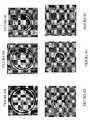
- FIGS. 1 A-Bshow a striking example of aligned nanotube pillars placed on specific sites on the substrate according to one aspect of the first embodiment.
- FIG. 1Aillustrates an SEM image of pillars of aligned carbon nanotube (CNT) arrays within trenches surrounded by a thick aligned nanotube film grown vertically on the SiO 2 pattern on a Si substrate. The nanotube film was selectively grown on a SiO 2 pattern or template structure. In the center of box-like regions defined by the nanotube film walls, micro-sized cylindrical blocks or pillars of vertically oriented nanotubes are grown from the underlying template structure constituted by SiO 2 patterns in this case. Within each block, the nanotubes are highly oriented and densely packed. Three different pillar packing densities are shown in FIG. 1A, where the separation between pillars in each group is 10 microns (top), 5 microns (bottom) and 2 microns (center).
- FIG. 1Bis an enlarged image of the middle array shown in FIG. 1A showing the alignment of the nanotubes in each of the pillars.
- FIG. 1Cillustrates a schematic of the nanotube pillars on the SiO 2 patterns located a Si substrate. Specifically, FIG. 1C shows a silicon substrate 10 containing cylindrical SiO 2 template structures 12 on the upper surface of the substrate 10 . Carbon nanotube pillars 14 are selectively grown and are located on the upper surfaces of the template structures 12 . Since the height (i.e., thickness) of the template structures 12 is less than a cutoff thickness for growth of nanotubes (such as less than 1 micron, preferably 200 nm or less), the nanotubes do not grow from the sidewalls of the template structures 12 . The cutoff thickness varies with the template material and with the nanotube growth parameters.
- FIGS. 1 A-Cwere made by the following method.
- the SiO 2 template structures or patterns 12were formed on a silicon substrate 10 by conventional photolithography.
- the template structures 12were exposed to xylenes/ferrocene gas mixtures at temperatures ranging from 600 to 1100° C., preferably 800 to 900° C. in a CVD tube furnace.
- the nanotubes 14grew extremely selectively on the SiO 2 patterns 12 , but did not grow on the silicon substrate 10 , leaving the exposed silicon substrate blank. Alignment of nanotubes can be easily identified from the sidewalls, which separate the micro pillar arrays of nanotubes.
- the template structureshad a diameter of about 10 microns to form cylindrical nanotube pillars having a diameter of about 10 microns in diameter and separations between individual pillars 14 of 10, 5 and 2 microns for the top, bottom and middle pillar sets, respectively.
- other suitable pillar 14 shapessuch as polygonal (triangular, rectangular, trapezoidal, etc.), oval or irregular shapes, can be fabricated by shaping the template structures 12 accordingly.
- SiO 2 template structures 12 on a silicon 10 substratewere illustrated, other suitable materials for the template structures 12 and the substrate 10 may be used instead, as described herein.
- FIG. 2Ais top view of several “sandwich” or rectangular block structures of platelets of aligned nanotubes grown from parallel silica lines (i.e., template structures) on a silicon substrate according to another preferred aspect of the first embodiment.
- the different sandwich structuresshow different nanotube platelet thickness (2-10 microns, decreasing from left to right in FIG. 2A) and separation between the platelets (2-10 microns, decreasing from left to right).
- the SiO 2 line patterns or template structureswere each 100 microns in length. They were fabricated using standard photolithography.
- the nanotube platelets or lineswere selectively grown on the template structures by the CVD method described above.
- the resultshows the excellent control of the placement of the nanotube platelet structures at the desired locations, their thickness, height and the separation between them (density).
- the height of these structurescan be precisely controlled to within a few tenths of microns to several hundreds of microns by tuning the nanotube deposition time.
- templates other than SiO 2 and substrate materials other than siliconmay be used instead.
- FIG. 2Bis a higher magnification SEM image showing the alignment of nanotubes within the nanotube platelets.
- the coordinated deformation and displacement of the individual platelets on the substrateindicate substantial attractive forces between individual nanotubes, suggesting that each platelet may be manipulated individually.
- FIGS. 2C and 2Dillustrate very long, ordered micro fibers of aligned nanotubes grown from silica patterns of two different shapes, resulting in two different fiber cross-sections, according to another aspect of the first embodiment.
- FIG. 2Cshows fibers with a circular cross section
- FIG. 2Dshows fibers with a square cross section.
- the cross-sections of these nanotube fibersare controlled by the shape of the underlying template patterns on which they grow.
- Plural nanotubes within each micro-fibercan grow simultaneously to hundreds of micrometers, aligned all along the length.
- the template structures or patterns 12 used to produce these fibersare essentially the same as those used for structures in FIGS.
- the fiberscan have a length of 100 to 500 microns, such as 150 to 300 microns, depending on the length of the nanotube deposition time.
- the present inventorsobserved good adhesion between individual nanotubes within each geometrical block, and between the nanotubes and the substrate.
- the nanotube blockscan be detached from the substrates by ultrasonic agitation, and can be manipulated individually using any suitable nanotube manipulation method.
- the removed nanotube pillars, platelets and/or fibersmay be selectively placed into a desired device, such as an electronic device.
- porous carbon nanotube filmswere fabricated. These porous films were fabricated with a high degree of control over pore sizes, shapes and separations. This is illustrated in FIGS. 3 A-C, which show nanotube films with regular arrays of pores. Three different pore features imprinted in the nanotube film are shown in FIGS. 3 A-C. For example, nanotube films with square and rectangular pores arranged in a rectangular grid are shown in FIGS. 3A and 3B, respectively. A nanotube film with randomly shaped pores arranged in a random orientation is shown in FIG. 3C. The porous carbon nanotube films shown in FIGS.
- 3 A-Cinclude a plurality of carbon nanotubes aligned lengthwise in a direction away from the template layer and a plurality of first pores extending through the film in the same direction.
- the bottom ends of the carbon nanotubesare attached to the porous template material such that the pores in the nanotube film have a controlled size and are aligned with the respective pores in the template material.
- the carbon nanotubesare not disposed on portions of the substrate exposed through the pores.
- the porous nanotube filmswere obtained by using a porous template structure or layer formed over a substrate.
- a porous silica template layerwas obtained by forming a silica layer on the silicon substrate and then photolithographically masking the layer and etching pores or holes in this layer. Since the pores or holes are formed by photolithography and etching, they have a controlled size. The pores or holes extend down to the silicon substrate and may extend into the silicon substrate if desired. Thus, portions of the substrate are exposed through pores in the porous template layer. Nanotube-forming gases or mixtures were provided onto the porous template layer and the carbon nanotubes were selectively grown on the porous template layer.
- the nanotubeswere not formed on portions of the substrate exposed through pores in the porous template layer. Furthermore, the nanotubes did not form on the template layer pore sidewalls because the template layer thickness is not sufficient to allow nanotube growth on side surfaces of the pores in the template layer.
- the template layermay have a thickness of less than about 200 nm, depending on the exact processing conditions and the template material used, to avoid nanotube growth on the side surfaces of the pores.
- the substratemay be selectively removed, such as by polishing or by silicon selective etching, to form a free standing porous nanotube film.
- the porous nanotube filmis produced by a different method.
- the template materialcan be selectively covered by noncatalytic masking materials (e.g., gold) through lithography and deposition, at locations where pores are desired.
- the template materialhas a plurality of first regions masked by a masking material which does not catalyze nanotubes, such as gold or copper masking material.
- the ends of the nanotubesare attached to the template material- such that the plurality of pores in the nanotube film have a controlled size and are aligned with the plurality of first regions on the template material masked by the masking material.
- the nanotubesWhen the nanotubes are grown on the masked template material, the nanotubes selectively grow on the exposed template material but not on the masked first regions of the template material.
- the template layermay be considered to be the negative pattern of the one used to make free-standing nanotube blocks shown in FIGS. 1 and 2. Both the number of nanotubes in each block (e.g., pillar), and the lateral separation between the blocks or pores are limited only by the smallest dimension of silica patterns that can be produced, and these can conceivably be made smaller by using electron-beam lithographed templates or templates made by other submicron lithography or patterning methods.
- nanotube growth on the template structurehaving at least one, and preferably two or more surfaces.
- the nanotube growthoccurs in a direction normal to the respective surfaces and hence this approach can be harnessed to simultaneously grow nanotubes in several predetermined directions.
- nanotube growth in mutually orthogonal directionsmay be carried out by using template structures comprising of deep etched trenches, drilled all the way to silicon substrate, separating several thick SiO 2 template structure towers.
- the nanotubesare grown on side surfaces of the template structures, which are preferably thicker than about 200 nm, preferably thicker than 2 microns.
- the template structuremay be several microns thick, such as 2 to 10 microns thick, preferably 5 to 8.5 microns thick.
- thickness of the template structure for growing controllably aligned nanotubes on the side surfaces of the template structurevaries based on the template material and the nanotube growth conditions. The preference of nanotubes to grow normal to, and selectively on, silica surfaces, forces the nanotubes to inherit the topography of the substrate templates, enabling the premeditation of both nucleation sites and growth direction.
- the template structure that is located on the substratehas at least one, and preferably two or more surfaces.
- a first plurality of carbon nanotubesare disposed on a first surface of the template structure. These first plurality of carbon nanotubes are controllably aligned in a first direction perpendicular to the first surface of the template structure.
- a second plurality of carbon nanotubesare disposed on a second surface of the template structure. This second plurality of carbon nanotubes are controllably aligned in a second direction perpendicular to the second surface of the template structure, such that the first direction is different than the second direction. The same applies for other surfaces of the template structures.
- FIGS. 4 A-Dillustrate vertically and horizontally aligned nanotube arrays adjacent to each other produced in a single-step growth process.
- FIG. 4Ais an SEM image of simultaneously vertically and horizontally aligned nanotube arrays of nanotubes grown on a template structure comprising a thick SiO 2 film with deep, etched trenches that separate alternating layers of SiO 2 and silicon.
- FIG. 4Bis an enlarged area marked by the white box in FIG. 4A.
- FIG. 4Billustrates three dimensional aligned vertical and horizontal growth of nanotubes. The length of nanotubes in both vertical and horizontal growth is about 60 microns.
- FIG. 4Cshows a cross-section of the specimen of FIG. 4A cut along the white line shown in FIG. 4A.
- the inset in FIG. 4Cis a higher magnification image that shows the perfect, controlled orthogonal alignment of the nanotube arrays.
- FIG. 4Dis a schematic illustration of the SEM images of FIGS. 4 A-C.
- the rectangular silica template structure 12is formed on a silicon substrate 10 .
- the controllably aligned nanotube structures or arrays 14are formed on the upper surface of the template structure 12 as well as in two orthogonal directions in the substrate plane itself (i.e., the nanotubes 14 are aligned parallel to the upper plane or surface of the substrate 10 ).
- the nanotubes 14 on the upper template structure 12 surfaceare perpendicular to the nanotubes 14 on plurality of side surfaces of the template structure 12 , and the nanotubes 14 on different template side surfaces are located in different (i.e., perpendicular) directions from each other.
- the nanotubes 14are controllably aligned in directions perpendicular to the plurality of the side surfaces of the template structure 12 .
- the template structure 12 shown in FIG. 5comprises a cylindrical pillar having a height of about 5 microns containing one continuous side surface.
- the carbon nanotubesare controllably aligned in a direction perpendicular to this side surface of the template structure.
- the nanotube domains or structures 14 in FIG. 5includes vertical and horizontal arrays of nanotubes.
- the short vertical block of nanotubes grown in the center of each patternis surrounded by radiating nanotube arrays (wings) grown on the side surface of the silica template structure.
- the nanotube wingswould not be perfectly horizontal (i.e., parallel to the substrate surface), but still perpendicular to the template surface.
- the structurecontains nanotubes packed with oblique inclinations, neither orthogonal nor planar or parallel with respect to the upper substrate plane, by using deep-trench template structures, such as silica structures, with inclined side surfaces.
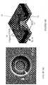
- FIGS. 6 A- 6 Gshow illustrative examples where nanotubes grow normal to the walls of such circular trenches, resulting in membrane iris-shaped structures having the shapes of open truncated cones.
- coneincludes the right circular cone with a circular base or directrix as well as structures having a curved (open or closed curve) or polygonal base or directrix to form pyramidal type structures with irregular or trapezoidal faces extending toward a common vertex.
- coneincludes any structure having a surface generated by a straight line passing though a fixed point and moving along the intersection with a fixed curve.
- FIG. 6His a schematic illustration of the cone shaped nanotube structures.
- the template structure 12 on the substrate 10contains an inclined side surface 16 and a flat upper surface.
- the inclined surface 16has an oblique inclination which is neither orthogonal nor parallel with respect to an upper plane of the substrate 10 .
- the nanotubes 14 on the upper surfacegrow perpendicular to this surface of the template structure 12 .
- the nanotubes 18 on the inclined side surface 16 of the template structureextend perpendicular to this surface 16 to form the cone shaped membrane.
- the free standing membrane structures 18 made of aligned nanotubes created in the shapes of open truncated conesmay have any desired size.
- the width of the membrane or the size of the openingcan be controlled by the pattern diameter, the angle of trench wall and the time of growth. Typical examples of different diameter, cone angle, size of opening of the nanotube membrane are shown in FIGS. 6 A-F.
- the diameter of the pattern structuresare 300 , 250 , 200 , 150 , 100 and 50 microns, respectively.
- FIG. 6Gshows an enlarged view of the 100 ⁇ m diameter structure in FIG. 6E to demonstrate the geometry of the nanotube membrane in this 3-D architecture.
- This cone shaped membraneis formed the same way as the previous nanotube structures.
- the nanotube source gasis provided onto the template structure 12 and the carbon nanotubes 18 are selectively grown on the inclined surface 16 of the template structure but not on exposed portions of the substrate 10 , such that the grown carbon nanotubes comprise a membrane having an open truncated cone shape.
- the nanotubes 14may also be grown on the upper surface of the template structure 12 or the upper surface of the template structure may be masked, as will be described below, to form only the nanotube membrane 18 on the template structure 12 .
- FIGS. 6 A-Galso show the flexibility of the method of the fourth embodiment to obtain radially oriented nanotubes with the entire spectrum of in-plane orientations relative to the substrate plane.
- the present inventorsproduced structures with different diameter, cone angle, size of opening and film thickness by tailoring the pattern dimensions, and growth time to control nanotube length.
- complex shapes of nanotube structurescan be generated by altering the trench geometry and depth.
- a masking layer or materialis formed on a portion of the template structure to selectively grow nanotubes only on an exposed portion of the template structure.
- a masking layeris a layer which inhibits growth of nanotubes on the template structure.
- a 2 to 20-nm-thick gold layercan be used as a masking material for silica template structures.
- Other examples of masking materialsinclude polysilicon, copper, or any other material that does not catalyze nanotube growth.
- the masking materialpreferably has a thickness at which it forms a continuous layer.
- a template structureis located on the substrate.
- a masking materialcovers a first portion of the template structure.
- a plurality of carbon nanotubesare located on a second portion of the template structure not covered by the masking material.
- the carbon nanotubesare not located on the masking material or on exposed portions of the substrate.
- a plurality of template structuresare located on the substrate.
- the method of the fifth preferred embodimentincludes providing a substrate containing a template structure having at least a portion covered by a masking material and providing a nanotube source gas onto the template structure.
- the methodalso includes selectively growing the carbon nanotubes on an exposed portion of the template structure but not on exposed portions of the substrate and not on portions of the template structure covered by the masking material.
- the methodprovides selective growth of nanotube bundles in controlled directions parallel to the substrate surface, by inhibiting nanotube growth from certain template structure portions or surfaces, such as the upper and/or some of the side surfaces.
- the lengths of CNTs growing in different directionscan be tuned by adjusting the masking material coverage and thickness respective template structure surfaces, the deposition time, and the SiO 2 pattern spacing. This allows fabrication of arrays of low-electrical resistance nanotube-metal contact structures that could be used to create nanotube-based electrical devices.
- FIGS. 7A and 7Bare schematic illustrations of a method of forming the masking material on the template structures.
- silicon ridges 11were photolithographically formed on a silicon substrate 10 .
- the substrate 10 and the ridges 11were covered with a thermally grown SiO 2 layer to form thermally-oxidized SiO 2 template structures 12 .
- Other suitable methods to form the template structuresmay be used if desired.
- a CVD SiO 2 layermay be patterned into template structures, as in the first embodiment.
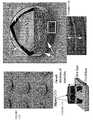
- FIG. 7Billustrates selective deposition of the gold masking layer on some surfaces of the template structure 12 .
- the substrate 10 containing the template structures 12was placed into a sputtering apparatus containing a sputtering target 20 and was tilted at 15 to 40 degrees, such as at 20 degrees relative to the target 20 .
- a gold masking layerwas then selectively sputtered onto the upper surfaces 22 and the left side surfaces 24 of the template structures.
- the right side surfaces 26 of the template structureswere not covered by the masking layer.
- a gold layerwas sputtered onto SiO 2 covered Si substrates in a 50 mTorr Ar plasma at an anode voltage of 7 V and a current of 25 mA, leading to an average deposition rate of about 1 nm s ⁇ 1 .
- the substrates with SiO 2 patternswere placed in a near-vertical configuration, at a tilt angle of about 20 degrees, with a sample-cathode distance of 30 mm. This sample placement geometry results in Au coverage on the top surface and one sidewall of each SiO 2 template structure that faces the Au flux, while the opposite sidewall is protected from Au coverage.
- the masking layermay be deposited by evaporation, sputtering, CVD or plating on the entire surface of the substrate and the template structures.
- the masking layermay then be photolithographically patterned to cover only the desired portions of the template structures 12 .
- the masking layercan be deposited only at desired locations by using a shadow mask, or through lift-off lithography techniques.
- the Au-coated SiO 2 template structureswere placed into a CVD tube furnace to grow carbon nanotubes selectively on exposed SiO 2 surfaces using a xylenes-ferrocene mixture. Substrates without Au coating were also loaded in the CVD furnace. A solution of 0.4 g ferrocene dissolved in 40 ml xylenes was fed into the CVD furnace at temperatures between 600 to 1100° C. for time intervals ranging from 5 to 30 minutes. This method produced aligned nanotubes, which were typically multiwalled nanotubes with diameters of about 20 to 50 nm.
- FIGS. 8 A- 8 Billustrate the growth behavior of carbon nanotubes (CNTs) on SiO 2 template structures that were not coated with Au before CVD.
- FIG. 8Aillustrates star-like growth of aligned CNTs on a row of SiO 2 template structures without Au coverage. The inset shows a schematic sketch of the morphology.
- FIG. 8Bis a high magnification view of FIG. 8A showing the CNT-CNT interface (see arrow) between SiO 2 patterns.
- the nanotubesgrow from all five surfaces of these template structure, i.e., the upper surface and four side surfaces, forming a star-like structure.
- the CNTs in each directionare well aligned, and have the same length of about 25 microns. CNTs growing in opposite directions, towards each other between patterns, cease to grow when they meet each other and form CNT-CNT interfaces as shown in FIG. 8B.
- FIGS. 8 C-Fillustrate selective CVD in-plane growth of aligned CNT bundles on exposed portions of template structures whose remaining portions were covered by a masking material.
- the selective growthis clearly in FIG. 8C, which shows 50 micron long CNT bridges grown from the left sidewalls of SiO 2 template structures whose upper and right sidewall surfaces were coated with Au.
- the CNTsform continuous nanotube bridges across a row of template structures.
- FIG. 8Eis a close-up view of the rectangular box in FIG. 8D, and shows a sharp interface between CNT tips and the template structure sidewall covered by Au where CNT growth stops.
- the inset in FIG. 8Eis a schematic illustration of the side-view of this interface.
- the process of selectively coating Au on different SiO 2 surfacescan be harnessed to controllably grow CNTs along any sets of in-plane directions.
- the nanotube growth directionwas reversed by coating Au on the upper surface and left sidewall of each template structure, as shown in FIG. 8F, compared to the direction shown in FIG. 8B.
- the CNT lengthis solely controlled by deposition time in the absence of physical obstacles in the growth direction.
- the CNTs grown from the last template structure in FIG. 8Fare about 80 microns long, while those grown between template structures are only 50 microns long, identical to the inter structure distance or spacing. This is a useful attribute in order to simultaneously bridge patterns with different inter-pattern distances by a single CVD process, where the growth time can be chosen to allow CNTs to bridge the longest inter structure gaps.
- nanotube bridgesmay be formed between different template structures in a single step even when a distance or spacing between a first and a second template structure differs from a distance or spacing between a second and a third template structure.
- the nanotube bridges which connect the first template structure to a second template structurediffer in length from those which connect the second template structure to the third template structure. These nanotube bridges extend parallel to a surface of the substrate.
- the nanotube source gasis provided for a sufficient time to allow the carbon nanotubes growing on the exposed portions of a one template structure to contact the masking material covering the covered portion of an adjacent template structure to form a nanotube bridge between these template structures. Furthermore, the nanotube source gas is provided for a sufficient time to simultaneously grow carbon nanotubes of a different length to allow the carbon nanotubes growing on the exposed portions of template structures to contact the masking material covering the covered portions of adjacent template structures.
- the growth timeis selected to allow the nanotubes to bridge the longest desired structure spacing or distance.
- FIGS. 8B and 8Falso show that CNTs grown on the two side-walls of SiO 2 patterns indicated by two tilted arrows in FIG. 8F are curled and shorter compared to the straight nanotube bundles between patterns. This result suggests that a lower Au coverage due to line-of-sight Au deposition on these SiO 2 surfaces leads to short nanotubes with less alignment.
- the present inventorsmeasured the length of CNTs grown on SiO 2 surfaces with different Au coverages.
- the Au coverageswere measured by RBS and varied between 0 and 1.1 ⁇ 10 17 atoms/cm 2 .
- FIG. 9Ais a plot of CNT length as a function of Au coverage on SiO 2 .
- the nominal Au film thicknessis also shown on the top axis.
- CVD conditionswere identical and the reaction time was 30 min.
- FIG. 9Bis an SEM image of Au islands (white contrast) on SiO 2 surface.
- FIG. 9Cis an SEM image of CNTs grown from the two sidewalls of a template structure with different lengths, 40 microns leftward from a SiO 2 surface partially covered by Au and 100 microns downward from a surface not covered by Au during the same deposition step.
- the plot in FIG. 9Ashows that CNT lengths decrease monotonically with increasing Au-atom coverage, and no nanotube growth is observed for Au coverages above 1.1 ⁇ 10 17 atoms/cm 2 (nominal Au thickness of about 20 nm). While present inventors do not want to be bound by any particular theory, they propose that the nanotube length decreases with increasing masking layer thickness according to the following mechanism. For Au coverages less than about 1.1 ⁇ 10 17 atoms/cm 2 , the as-deposited Au layer on SiO 2 is discontinuous and has an island morphology, as shown in FIG. 9B. It is assumed that the Au islands decrease the intake and interactions of carbon/catalyst flux with SiO 2 , and alter the nanotube growth rate.
- the Au layeris continuous and masks the entire SiO 2 surface, thus completely preventing CNT growth.
- the CNT length-dependence on the Au-coverageis useful for obtaining CNTs of tunable lengths along different directions through control of Au coverage on different faces of SiO 2 patterns, as shown in FIG. 9C.
- a first material which facilitates growth of carbon nanotubessuch as a silica or other suitable material layer or structure is provided. At least a portion of the first material is covered with a masking material, such as Au or another material which inhibits CNT growth. A nanotube source gas is provided onto the first material. The carbon nanotubes of a first length are selectively grown on an exposed portion of the first material. If the masking material is thicker than a critical thickness at which it comprises a continuous layer (e.g., Au layer with nominal thickness of greater than about 20 nm), then no CNTs are grown on the masking material.
- a critical thickness at which it comprises a continuous layere.g., Au layer with nominal thickness of greater than about 20 nm
- the masking materialis thinner than a critical thickness at which it comprises a continuous layer (i.e., such as an about 20 nm or thinner Au layer), then shorter CNTs of a second length less than the first length are growth on the masking material.
- a critical thickness at which it comprises a continuous layeri.e., such as an about 20 nm or thinner Au layer
- shorter CNTs of a second length less than the first lengthare growth on the masking material.
- a plurality of CNTs of different lengthmay be controllably grown during the same deposition step.
- the growth methodincludes providing a growth surface which facilitates growth of carbon nanotubes, providing a nanotube source gas onto the growth surface, and controllably growing the carbon nanotubes of different length during the same deposition step.
- FIG. 10Ais a schematic sketch of configuration used to measure the electrical resistance.
- the unbridged samplewas prepared using a short CVD time so that CNTs did not grow long enough to connect adjacent SiO 2 template structure.
- Two bridged sampleswere also prepared. During the measurements, one probe was fixed at P 0 , while another probe was moved to different locations from P 1 , to P 10 , to record the resistances across different number of CNT bridges.
- FIG. 10Bis a plot of resistance as a function of number of CNT bridges. Circles and squares show the resistance behavior for structures with CNT bridges, while triangles show data obtained from unbridged structures. R unbridged is due to the Au layer sputtered on the substrate area between SiO 2 patterns.
- the fifth preferred embodimentprovides in-plane growth of CNTs in predefined directions and with tunable lengths by selective masking of SiO 2 template structures with a metal that does not catalyze nanotube growth compared to silica.
- This methodcan be used to create nanotube bridges that interconnect SiO 2 patterns and provide low-resistance pathways for electrical transport.
- the methods which combine CVD with topographical masking of patterned substratesmay be used for controllably growing nanotube-metal architectures for electronic switching, memory storage, sensing and actuation devices.
- a structure of the sixth preferred embodimentincludes at least one suspended template material layer.
- a first aligned carbon nanotube layeris located on a first surface of the template material layer.
- a second aligned carbon nanotube layeris located on a second surface of the template material layer, located opposite to the first surface.
- a bilayer of aligned carbon nanotubescontains a suspended template layer between them. The nanotubes extend away from the respective surface of the template layer. If desired, three or more layers of aligned carbon nanotubes may be formed on two or more template layers.
- the suspended template material layermay be a template material cantilever or membrane supported on a portion of a substrate that does not catalyze carbon nanotube growth. If the template layer has sufficient thickness, then a third aligned carbon nanotube layer is located on an edge surface of the template material layer, such that the third aligned carbon nanotube layer is located perpendicular to the first and the second aligned carbon nanotube layers.
- FIG. 11Aillustrates a low magnification SEM image showing a bilayer of aligned carbon nanotubes grown at a 180 degree angle with respect to each other (up and down) from the top and bottom surfaces of a suspended, circular SiO 2 cantilever layer suspended on a Si base pillar.
- a suspended template material and substrate/basemay also be used.
- the template layermay comprise a membrane (i.e., a suspended layer supported on two or more sides or on two or more portions of a surface) rather than a cantilever (i.e., a suspended layer supported on one side or on one portion of a surface).
- the template layermay also contain both edge cantilever portions and a central membrane portion, if desired.
- FIG. 11BThe two growth directions from the SiO 2 surfaces (inset) and a schematic illustration of nanotube bilayer growth are shown in FIG. 11B.
- the SiO 2 layertransparent
- FIGS. 11B and 11CThis pattern of suspended SiO 2 templates with two exposed surfaces was generated by undercutting the silica layer located on a silicon substrate into the substrate during deep etching of about 40-50 microns.
- the template layer in FIGS. 11 A-Bdoes not have sufficient thickness to grow nanotubes on its edge surface.
- the nanotube growth directionsare shown by the arrows in FIG. 11C.
- FIGS. 12 A-Bare schematic sketches showing simultaneous multilayer and multidirectional growth of oriented nanotubes from thick (e.g., 2 microns or more) SiO 2 layer suspended on deep etched Si pillars.
- FIG. 12Ais a schematic of a silicon substrate with a thick cantilever SiO 2 layer suspended on a Si base before nanotube deposition.
- FIG. 12Bis a schematic of the nanotube growth on the suspended SiO 2 layer in three orientations. Since the silica layer is sufficiently thick, a nanotube layer growth from the edge surface of the suspended silica layer.
- FIG. 12Cis an SEM micrograph showing the aligned nanotubes extending in three directions marked by arrows. Thus, as shown in FIGS.
- the nanotubesmay extend from a suspended template layer toward an upper surface of the substrate at a 90 degree angle. However, the nanotubes may extend towards the substrate at any suitable angle, such as at a 30-160 degree angle, depending on the orientation of the template layer.
- nanotube networksmay be used in diverse applications such as nanotube-based electronic devices, micro and nano-electromechanical systems, micro- and nano-size porous supports and membranes for catalysis, fluidics and separation, and skeletal reinforcements for composites.
- the present inventorshave achieved excellent control and flexibility in designing and fabricating a wide variety of carbon nanotube architectures, as discussed in the preferred embodiments.
- Several ordered nanotube based structural elements of different orientationsmay be integrated onto one substrate by combining standard lithography techniques with a substrate-selective CNT CVD growth process effected by gas-phase delivery of catalysts. Structures such as micro-fibers and membranes containing highly aligned nanotubes can fabricated and could find use in nanocomposites and electrode systems.
- the fabrication method described hereis far easier and more versatile than the prior art methods.
- the preferred methoddoes not require a metal catalyst patterning step, thus simplifying the method to a great degree and providing better control, particularly for the catalyst particle size, for the growth process.
- the preferred methodis also scalable over large areas for commercial production with the aid of fabrication techniques commonly used in silicon microfabrication technology.
Landscapes
- Chemical & Material Sciences (AREA)
- Engineering & Computer Science (AREA)
- Materials Engineering (AREA)
- Organic Chemistry (AREA)
- Manufacturing & Machinery (AREA)
- Nanotechnology (AREA)
- Ceramic Engineering (AREA)
- Inorganic Chemistry (AREA)
- Crystallography & Structural Chemistry (AREA)
- Structural Engineering (AREA)
- Condensed Matter Physics & Semiconductors (AREA)
- General Physics & Mathematics (AREA)
- Physics & Mathematics (AREA)
- Metallurgy (AREA)
- Composite Materials (AREA)
- Chemical Kinetics & Catalysis (AREA)
- Electrochemistry (AREA)
- General Chemical & Material Sciences (AREA)
- Carbon And Carbon Compounds (AREA)
Abstract
Description
- The present application claims benefit under 35 U.S.C. §119(e) of U.S. provisional applications 60/356,069, filed Feb. 11, 2002 and 60/385,393, filed Jun. 3, 2002, both of which are incorporated herein by reference in their entirety.[0001]
- [0002] The U.S. Government may have certain rights in this invention pursuant to grant number N00014-00-1-2050 from the Office of Naval Research.
- The present invention relates generally to carbon nanotubes and more particularly to selective growth of carbon nanotubes on template materials.[0003]
- It is likely that future devices containing organized structures of various functional materials with new properties will be built from nanoscale building blocks. These nanoscale building blocks can be produced by a variety of synthesis routes. The novel properties of the nanoscale building blocks arising from their low dimensions are known for a wide range of materials.[0004]
- Carbon nanotubes are a nanostructured material which promises to have a wide range of applications. However, the present techniques used to controllably build organized architectures of nanotubes with predetermined orientations have several deficiencies. For example, vertically aligned nanotubes has been fabricated on catalyst printed planar substrates by chemical vapor deposition. See, for example, W. Z. Li, et al. Science 274, 1701 (1996); R. Sen, A. Govindaraj, C. N. R. Rao, Chem. Phys. Lett. 267, 276 (1997); M. Terrones, et al. Nature 388, 52 (1997); Z. F. Ren, et al. Science 282, 1105 (1998); S. S. Fan, et al. Science 283, 512 (1999); H. Kind, et al. Adv. Mater. 11, 1285 (1999); R. R. Schlittler, et al. Science 292, 1136 (2001) and L. Dai, A. W. H. Mau, J. Phys. Chem. B 104, 1891 (2000). However, this technique requires deposition and patterning, usually in separate processing steps, of catalyst material, typically in nanoparticle assemblies or thin film forms, which complicates the nanotube fabrication method. This also does not allow growth of nanotubes in more than one preselected orientation at different locations in a controllable fashion.[0005]
- While growth of vertically aligned nanotubes on planar substrates by CVD has been reported extensively, obtaining nanotubes that are exclusively oriented parallel to the substrate in predetermined orientations has been more difficult. Suspended nanotubes across elevated structures have been produced recently by several different methods. One method involves adjusting the gas flow during CVD. See N. R. Franklin, H. Dai, Adv. Mater. 2000, 12, 890; N. R. Franklin, Q. Wang, T. W. Tombler, A. Javey, M. Shim, H. Dai, Appl. Phys. Lett. 2002, 81, 913; and Y. Homma, Y. Kobayashi, T. Ogino, T. Yamashita, Appl. Phys. Lett. 2002, 81, 2261. Another method involves applying an electrical field during CVD. See Y. Zhang, A. Chang, J. Cao, Q. Wang, W. Kim, Y. Li, N. Morris, E. Yenilmez, J. Kong, H. Dai, Appl. Phys. Lett. 2001, 79, 3155; and A. Ural, Y. Li, H. Dai, Appl. Phys. Lett. 2002, 81, 3464. However, these approaches require pre-deposition and pre-patterning of nanoscale catalyst particle assemblies. Also, the probability of nanotubes bridging across different catalyst islands is difficult to predict and control. Several articles also note that nanotubes can be aligned in horizontal configurations through electric fields or microfluidic forces. See A. Star, et al., Angewandte Chem. International Edition 40, 1721 (2001) and T. Rueckes, et al., Science 289, 94 (2000). However, these methods are also complicated, and are difficult to scale (e.g., create them reproducibly on an 8 inch Si wafer) and to control, for developing devices for applications. Moreover, in these cases the nanotubes are not rooted to the substrate (i.e. they are just lying on them, and hence not very robust).[0006]
- Several methods have also been suggested for controlled placement of carbon nanotubes onto electrode pairs, including AC bias-enhanced deposition and chemically modified adsorption. See L. A. Nagahara, I. Amiani, J. Lewenstein, R. K. Tsui, Appl. Phys. Lett. 2002, 80, 3826 and M. Burgard, G. Buesberg, G. Philipp, J. Muster, S. Roth, Adv. Mater. 1998, 10, 584.[0007]
- Some of the present inventors have also previously suggested to selectively grow carbon nanotubes on silica templates located on a silicon substrate without growing the nanotubes on the silicon substrate. See Z. J. Zhang, B. Q. Wei, G. Ramanath, P. M. Ajayan, Appl. Phys. Lett. 77, 3764 (2000). The use of this template structure is advantageous in that it does not require the deposition and patterning of the catalyst material. However, as can be seen in FIG. 4 of the Z. J. Zhang et al. article, while roughly vertical and horizontal nanotubes were simultaneously grown on the template structures, it was not possible to controllably align nanotubes during growth in a direction perpendicular to the silica template structure surfaces. For example, as shown in the insert in FIG. 4 of this article, the nanotubes were not aligned precisely and controllably.[0008]
- A preferred embodiment of the invention provides a method of making carbon nanotubes, comprising providing a substrate containing a template structure having at least two surfaces and providing a nanotube source gas onto the template structure. The nanotube source gas preferably comprises a mixture of nanotube forming precursor gas, such as xylenes, and a catalyst gas, such as ferrocene. However, other suitable gases or a single source gas may be used instead. The method further provides for selectively and simultaneously growing the carbon nanotubes on the at least two surfaces of the template structure but not on exposed portions of the substrate (i.e., in exclusion to the substrate material which supports the template structure). The grown carbon nanotubes are controllably aligned in a direction perpendicular to the respective surfaces of the template structure.[0009]
- Another preferred embodiment of the invention provides a structure, comprising a substrate and a template structure located on the substrate, wherein the template structure comprises at least two surfaces. The structure also comprises a first plurality of carbon nanotubes disposed on a first surface of the template structure, wherein the first plurality of carbon nanotubes are controllably aligned in a first direction perpendicular to the first surface of the template structure, and a second plurality of carbon nanotubes disposed on a second surface of the template structure, wherein the second plurality of carbon nanotubes are controllably aligned in a second direction perpendicular to the second surface of the template structure, such that the first direction is different than the second direction.[0010]
- FIGS.[0011]1A-B,2A-D,4A-C,5,6A-G,8A-F,9C,11A-B and12C are SEM images of carbon nanotube structures according to preferred embodiments of the present invention.
- FIGS. 2C, 4D,[0012]6H,11C and12A-B are three dimensional schematics of carbon nanotube structures according to preferred embodiments of the present invention.
- FIGS.[0013]3A-3C are SEM images of porous carbon nanotube films according to a preferred embodiment of the present invention.
- FIGS.[0014]7A-B are side cross sectional schematic views of a method of making carbon nanotube structures according to a preferred embodiment of the present invention.
- FIG. 9A is a plot of carbon nanotube length as a function of gold masking material coverage on a SiO[0015]2template structure according to a preferred embodiment of the present invention.
- FIG. 9B is an SEM image of gold masking material islands on a surface of a SiO[0016]2template structure according to a preferred embodiment of the present invention.
- FIG. 10A is side cross sectional schematic view of carbon nanotube structures according to a preferred embodiment of the present invention.[0017]
- FIG. 10B is a plot of measured resistance versus a number of carbon nanotube bridges according to a preferred embodiment of the present invention.[0018]
- The present inventors have developed a method of controllably aligning carbon nanotubes to a template structure to fabricate a variety of carbon nanotube containing structures and devices having desired characteristics. For example, by selecting a template structure with a sufficient thickness allows a simultaneous growth of both vertically and horizontally controllably aligned nanotubes in a single process step. In fact, the nanotubes may be aligned in any set of in-plane and/or out of plane orientations and grown in a single process step. The level of control provided by this method provides construction of complex, nanotube based, highly organized 1-to-3-D architectures for building or use in nanotube based devices and systems in a scalable fashion.[0019]
- A template structure, pattern or material is a structure, pattern or material which allows selective growth of carbon nanotubes on it without growing any detectable amount of carbon nanotubes on exposed portions of the substrate which supports the template. Nanotubes grow normal to, and selectively on the template structure, inheriting the topography of the template structure. Thus, the nanotubes are controllably aligned in a direction perpendicular to the surface of the template structure from which they grow such that all the nanotubes which grow from a particular template structure surface are oriented in the same direction. The precise control of nanotube orientation allows the fabrication of a wide variety of organized architectures of differing complexities, shapes, densities, dimensions and orientation. The bottom up fabrication approach is easy, scalable, and compatible with silicon microfabrication techniques and processes.[0020]
- In a preferred aspect of the present invention, the template structure comprises a silicon dioxide structure located on a silicon substrate. However, other suitable template and substrate materials may be used instead. For example, other silicon oxide and metal oxide template structures materials, such as silicon oxynitride, magnesium oxide, aluminum oxide or indium tin oxide, may be used instead. Thus, a carbon nanotube growth catalyst material, such as a metal nanoparticle layer, is not necessary to selectively grow carbon nanotubes, and is preferably omitted to simplify processing. In alternative aspects of the present invention, a metal that does not catalyze nanotube growth, such as gold or copper, can also be used to mask part of the template structure material on the substrate. The substrate material can be any material that does not catalyze nanotube growth. Examples of preferred substrate materials are a single crystal silicon wafer, epitaxial silicon and polysilicon layers. Furthermore, other semiconductor materials, such as II-VI and III-V semiconductor materials, and non-semiconductor materials, such as ceramics, metals, glasses and plastics that do not catalyze nanotube growth may be used as a substrate by appropriately selecting the template material which allows selective growth of carbon nanotubes.[0021]
- In another alternative aspect of the present invention, the substrate may be omitted entirely, and the nanotubes may be fabricated on free standing template structures. For example carbon nanotubes may be formed on the surfaces of oxide particles, such as silica, alumina, MgO and other silicon and metal oxide particles. Preferably, the particles are substantially spherical oxide particles, such as spherical, oval and roughly spherical (i.e., spherical particles with chiseled surfaces) particles. The particles may be micro sized (preferably 1 to 1,000 micron diameter) or macro sized (preferably 1,000 microns to 1 cm diameter). The carbon nanotubes are aligned perpendicular to the oxide particle surfaces.[0022]
- In preferred embodiments of the present invention, controllably aligned multiwalled carbon nanotubes are selectively and simultaneously grown in patterns and in multiple directions on lithographically patterned silica templates in a single process. This process is preferably carried out through a CVD method that delivers the nanotube-forming precursor and the catalyst material (in compound or elemental form) from the gas phase either simultaneously or sequentially.[0023]
- The specific examples of nanotube structures of the present invention shown are illustrated in SEM images in the Figures. However, the present invention should not be considered limited by the structures and methods of the specific examples, which are provided for illustration of the present invention.[0024]
- The nanotube structures shown in the SEM images in the Figures were selectively grown on non-planar patterns composed of SiO[0025]2and Si surfaces. The substrates were Si (100) wafers capped with thermally grown or plasma-enhanced chemical vapor deposition (PECVD) deposited SiO2template structures having a thickness of 100 nm to several microns, such as 2 to 8.5 microns. For example, thick silica layers (up to about 8.5 microns) were deposited by PECVD to create high-aspect-ratio silica features. Patterns of Si/SiO2of various shapes were generated by photolithography followed by a combination of wet and/or dry etching.
- Patterned nanotube growth was achieved without metal catalyst predeposition and patterning, thereby simplifying the template preparation by eliminating 2 processing steps. Instead, CVD nanotube growth was stimulated by exposing the substrate and the template structure on the substrate to vapor mixtures comprising xylenes (C[0026]8H10), a nanotube-forming precursor, and ferrocene (Fe(C5H5)2), a nanotube catalyst, at about 600 to 1100° C., preferably at about 800 to 900° C. However, other suitable source gases and temperatures may be used instead. Ferrocene was dissolved in xylenes (which preferably contains different isomers) at concentrations of about 0.01 g/ml, the mixture was pre-heated, co-evaporated and fed into the CVD chamber. Ferrocene preferably comprises 0.001 to 1 percent of the ferrocene/xylenes mixture. Prolonged growth in the temperature range of 600-1100° C., produced films of densely packed multiwalled carbon nanotubes on the template structures but not on the substrate. Uniform, vertically aligned nanotube films having a thickness of a few microns to several tens of microns were produced in few minutes at growth rates of about 10 microns/minute. The nanotubes in the nanotube films were about 30 nm diameter multiwalled carbon nanotubes. No nanotube growth was observed on pristine Si surfaces, or on the native oxide layer formed on the silicon substrate. Aligned nanotubes grew readily on SiO2templates in a direction normal to the template growth surface, and the selectivity was retained down to micron size SiO2templates.
- Using the substrate-selective and normal direction growth process, the nanotubes structures of various shapes and orientations with respect to the Si surface were fabricated on active SiO[0027]2template surfaces. Thus, carbon nanotubes were selectively grown in desired patterns and architectures without further photolithographic patterning.
- The method and structure of the first preferred embodiment will now be described. In the first preferred embodiment, the carbon nanotubes were selectively grown in one direction on various template structure shapes to produce various nanotube structure shapes having the footprint of the template surfaces. These nanotube structures can then be optionally removed from over the substrate and placed into a suitable device.[0028]
- FIGS.[0029]1A-B show a striking example of aligned nanotube pillars placed on specific sites on the substrate according to one aspect of the first embodiment. FIG. 1A illustrates an SEM image of pillars of aligned carbon nanotube (CNT) arrays within trenches surrounded by a thick aligned nanotube film grown vertically on the SiO2pattern on a Si substrate. The nanotube film was selectively grown on a SiO2pattern or template structure. In the center of box-like regions defined by the nanotube film walls, micro-sized cylindrical blocks or pillars of vertically oriented nanotubes are grown from the underlying template structure constituted by SiO2patterns in this case. Within each block, the nanotubes are highly oriented and densely packed. Three different pillar packing densities are shown in FIG. 1A, where the separation between pillars in each group is 10 microns (top), 5 microns (bottom) and 2 microns (center).
- FIG. 1B is an enlarged image of the middle array shown in FIG. 1A showing the alignment of the nanotubes in each of the pillars. FIG. 1C illustrates a schematic of the nanotube pillars on the SiO[0030]2patterns located a Si substrate. Specifically, FIG. 1C shows a
silicon substrate 10 containing cylindrical SiO2template structures12 on the upper surface of thesubstrate 10.Carbon nanotube pillars 14 are selectively grown and are located on the upper surfaces of thetemplate structures 12. Since the height (i.e., thickness) of thetemplate structures 12 is less than a cutoff thickness for growth of nanotubes (such as less than 1 micron, preferably 200 nm or less), the nanotubes do not grow from the sidewalls of thetemplate structures 12. The cutoff thickness varies with the template material and with the nanotube growth parameters. - The structures shown in FIGS.[0031]1A-C were made by the following method. The SiO2template structures or
patterns 12 were formed on asilicon substrate 10 by conventional photolithography. Thetemplate structures 12 were exposed to xylenes/ferrocene gas mixtures at temperatures ranging from 600 to 1100° C., preferably 800 to 900° C. in a CVD tube furnace. Thenanotubes 14 grew extremely selectively on the SiO2patterns12, but did not grow on thesilicon substrate 10, leaving the exposed silicon substrate blank. Alignment of nanotubes can be easily identified from the sidewalls, which separate the micro pillar arrays of nanotubes. The template structures had a diameter of about 10 microns to form cylindrical nanotube pillars having a diameter of about 10 microns in diameter and separations betweenindividual pillars 14 of 10, 5 and 2 microns for the top, bottom and middle pillar sets, respectively. In addition to thecylindrical pillars 14 andcylindrical template structures 12, othersuitable pillar 14 shapes, such as polygonal (triangular, rectangular, trapezoidal, etc.), oval or irregular shapes, can be fabricated by shaping thetemplate structures 12 accordingly. Furthermore, while SiO2template structures12 on asilicon 10 substrate were illustrated, other suitable materials for thetemplate structures 12 and thesubstrate 10 may be used instead, as described herein. - FIG. 2A is top view of several “sandwich” or rectangular block structures of platelets of aligned nanotubes grown from parallel silica lines (i.e., template structures) on a silicon substrate according to another preferred aspect of the first embodiment. The different sandwich structures show different nanotube platelet thickness (2-10 microns, decreasing from left to right in FIG. 2A) and separation between the platelets (2-10 microns, decreasing from left to right). The SiO[0032]2line patterns or template structures were each 100 microns in length. They were fabricated using standard photolithography. The nanotube platelets or lines were selectively grown on the template structures by the CVD method described above. The result shows the excellent control of the placement of the nanotube platelet structures at the desired locations, their thickness, height and the separation between them (density). The height of these structures can be precisely controlled to within a few tenths of microns to several hundreds of microns by tuning the nanotube deposition time. Of course shapes other than rectangular platelets, template materials other than SiO2and substrate materials other than silicon may be used instead.
- FIG. 2B is a higher magnification SEM image showing the alignment of nanotubes within the nanotube platelets. The coordinated deformation and displacement of the individual platelets on the substrate indicate substantial attractive forces between individual nanotubes, suggesting that each platelet may be manipulated individually.[0033]
- FIGS. 2C and 2D illustrate very long, ordered micro fibers of aligned nanotubes grown from silica patterns of two different shapes, resulting in two different fiber cross-sections, according to another aspect of the first embodiment. FIG. 2C shows fibers with a circular cross section and FIG. 2D shows fibers with a square cross section. Thus, the cross-sections of these nanotube fibers are controlled by the shape of the underlying template patterns on which they grow. Plural nanotubes within each micro-fiber can grow simultaneously to hundreds of micrometers, aligned all along the length. The template structures or[0034]
patterns 12 used to produce these fibers are essentially the same as those used for structures in FIGS.1A-C, but the growth time is longer resulting in flexible ordered fibers, compared to stiffer, shorter pillars of FIGS.1A-C. The fibers can have a length of 100 to 500 microns, such as 150 to 300 microns, depending on the length of the nanotube deposition time. - In all cases of the nanotube pillars shown in FIGS.[0035]1A-C, the nanotube platelets shown in FIGS.2A-B and the nanotube fibers shown in FIGS.2C-D, the present inventors observed good adhesion between individual nanotubes within each geometrical block, and between the nanotubes and the substrate. The nanotube blocks, however, can be detached from the substrates by ultrasonic agitation, and can be manipulated individually using any suitable nanotube manipulation method. For example, the removed nanotube pillars, platelets and/or fibers may be selectively placed into a desired device, such as an electronic device.
- The method and structure of the second preferred embodiment will now be described. In the second preferred embodiment, porous carbon nanotube films were fabricated. These porous films were fabricated with a high degree of control over pore sizes, shapes and separations. This is illustrated in FIGS.[0036]3A-C, which show nanotube films with regular arrays of pores. Three different pore features imprinted in the nanotube film are shown in FIGS.3A-C. For example, nanotube films with square and rectangular pores arranged in a rectangular grid are shown in FIGS. 3A and 3B, respectively. A nanotube film with randomly shaped pores arranged in a random orientation is shown in FIG. 3C. The porous carbon nanotube films shown in FIGS.3A-C include a plurality of carbon nanotubes aligned lengthwise in a direction away from the template layer and a plurality of first pores extending through the film in the same direction. The bottom ends of the carbon nanotubes are attached to the porous template material such that the pores in the nanotube film have a controlled size and are aligned with the respective pores in the template material. The carbon nanotubes are not disposed on portions of the substrate exposed through the pores.
- The porous nanotube films were obtained by using a porous template structure or layer formed over a substrate. For example, a porous silica template layer was obtained by forming a silica layer on the silicon substrate and then photolithographically masking the layer and etching pores or holes in this layer. Since the pores or holes are formed by photolithography and etching, they have a controlled size. The pores or holes extend down to the silicon substrate and may extend into the silicon substrate if desired. Thus, portions of the substrate are exposed through pores in the porous template layer. Nanotube-forming gases or mixtures were provided onto the porous template layer and the carbon nanotubes were selectively grown on the porous template layer. However, the nanotubes were not formed on portions of the substrate exposed through pores in the porous template layer. Furthermore, the nanotubes did not form on the template layer pore sidewalls because the template layer thickness is not sufficient to allow nanotube growth on side surfaces of the pores in the template layer. For example, the template layer may have a thickness of less than about 200 nm, depending on the exact processing conditions and the template material used, to avoid nanotube growth on the side surfaces of the pores. If desired, after the nanotube film is grown, the substrate may be selectively removed, such as by polishing or by silicon selective etching, to form a free standing porous nanotube film. In an alternative aspect of the second embodiment, the porous nanotube film is produced by a different method. The template material can be selectively covered by noncatalytic masking materials (e.g., gold) through lithography and deposition, at locations where pores are desired. The template material has a plurality of first regions masked by a masking material which does not catalyze nanotubes, such as gold or copper masking material. The ends of the nanotubes are attached to the template material- such that the plurality of pores in the nanotube film have a controlled size and are aligned with the plurality of first regions on the template material masked by the masking material. When the nanotubes are grown on the masked template material, the nanotubes selectively grow on the exposed template material but not on the masked first regions of the template material.[0037]
- Thus, the template layer may be considered to be the negative pattern of the one used to make free-standing nanotube blocks shown in FIGS. 1 and 2. Both the number of nanotubes in each block (e.g., pillar), and the lateral separation between the blocks or pores are limited only by the smallest dimension of silica patterns that can be produced, and these can conceivably be made smaller by using electron-beam lithographed templates or templates made by other submicron lithography or patterning methods.[0038]
- The method and structure of the third preferred embodiment will now be described. In the third embodiment, selective nanotube growth on the template structure having at least one, and preferably two or more surfaces. The nanotube growth occurs in a direction normal to the respective surfaces and hence this approach can be harnessed to simultaneously grow nanotubes in several predetermined directions. For example, nanotube growth in mutually orthogonal directions may be carried out by using template structures comprising of deep etched trenches, drilled all the way to silicon substrate, separating several thick SiO[0039]2template structure towers. Preferably, the nanotubes are grown on side surfaces of the template structures, which are preferably thicker than about 200 nm, preferably thicker than 2 microns. For example, the template structure may be several microns thick, such as 2 to 10 microns thick, preferably 5 to 8.5 microns thick. However, thickness of the template structure for growing controllably aligned nanotubes on the side surfaces of the template structure varies based on the template material and the nanotube growth conditions. The preference of nanotubes to grow normal to, and selectively on, silica surfaces, forces the nanotubes to inherit the topography of the substrate templates, enabling the premeditation of both nucleation sites and growth direction.
- Preferably, the template structure that is located on the substrate has at least one, and preferably two or more surfaces. A first plurality of carbon nanotubes are disposed on a first surface of the template structure. These first plurality of carbon nanotubes are controllably aligned in a first direction perpendicular to the first surface of the template structure. Furthermore, a second plurality of carbon nanotubes are disposed on a second surface of the template structure. This second plurality of carbon nanotubes are controllably aligned in a second direction perpendicular to the second surface of the template structure, such that the first direction is different than the second direction. The same applies for other surfaces of the template structures.[0040]
- FIGS.[0041]4A-D illustrate vertically and horizontally aligned nanotube arrays adjacent to each other produced in a single-step growth process. FIG. 4A is an SEM image of simultaneously vertically and horizontally aligned nanotube arrays of nanotubes grown on a template structure comprising a thick SiO2film with deep, etched trenches that separate alternating layers of SiO2and silicon. FIG. 4B is an enlarged area marked by the white box in FIG. 4A. FIG. 4B illustrates three dimensional aligned vertical and horizontal growth of nanotubes. The length of nanotubes in both vertical and horizontal growth is about 60 microns. The thickness of SiO2patterns was 8.5 microns, which is thicker than a threshold required to grow controllably aligned nanotubes on side surfaces. FIG. 4C shows a cross-section of the specimen of FIG. 4A cut along the white line shown in FIG. 4A. The inset in FIG. 4C is a higher magnification image that shows the perfect, controlled orthogonal alignment of the nanotube arrays.
- FIG. 4D is a schematic illustration of the SEM images of FIGS.[0042]4A-C. The rectangular
silica template structure 12 is formed on asilicon substrate 10. The controllably aligned nanotube structures orarrays 14 are formed on the upper surface of thetemplate structure 12 as well as in two orthogonal directions in the substrate plane itself (i.e., thenanotubes 14 are aligned parallel to the upper plane or surface of the substrate10). Thus, thenanotubes 14 on theupper template structure 12 surface are perpendicular to thenanotubes 14 on plurality of side surfaces of thetemplate structure 12, and thenanotubes 14 on different template side surfaces are located in different (i.e., perpendicular) directions from each other. Thus, thenanotubes 14 are controllably aligned in directions perpendicular to the plurality of the side surfaces of thetemplate structure 12. - Another preferred aspect of the third embodiment is illustrated in FIG. 5. In this aspect, the[0043]
template structure 12 shown in FIG. 5 comprises a cylindrical pillar having a height of about 5 microns containing one continuous side surface. The carbon nanotubes are controllably aligned in a direction perpendicular to this side surface of the template structure. The nanotube domains orstructures 14 in FIG. 5 includes vertical and horizontal arrays of nanotubes. The short vertical block of nanotubes grown in the center of each pattern is surrounded by radiating nanotube arrays (wings) grown on the side surface of the silica template structure. If wet etching of the thicksilica template structure 12 creates inclined side surfaces (forming a frustum rather than a perfect cylinder), then the nanotube wings would not be perfectly horizontal (i.e., parallel to the substrate surface), but still perpendicular to the template surface. - The method and structure of the fourth preferred embodiment will now be described. In the fourth embodiment, the structure contains nanotubes packed with oblique inclinations, neither orthogonal nor planar or parallel with respect to the upper substrate plane, by using deep-trench template structures, such as silica structures, with inclined side surfaces. FIGS.[0044]6A-6G show illustrative examples where nanotubes grow normal to the walls of such circular trenches, resulting in membrane iris-shaped structures having the shapes of open truncated cones.
- The term “cone” includes the right circular cone with a circular base or directrix as well as structures having a curved (open or closed curve) or polygonal base or directrix to form pyramidal type structures with irregular or trapezoidal faces extending toward a common vertex. Thus, “cone” includes any structure having a surface generated by a straight line passing though a fixed point and moving along the intersection with a fixed curve.[0045]
- FIG. 6H is a schematic illustration of the cone shaped nanotube structures. The[0046]
template structure 12 on thesubstrate 10 contains aninclined side surface 16 and a flat upper surface. Theinclined surface 16 has an oblique inclination which is neither orthogonal nor parallel with respect to an upper plane of thesubstrate 10. Thenanotubes 14 on the upper surface grow perpendicular to this surface of thetemplate structure 12. Thenanotubes 18 on theinclined side surface 16 of the template structure extend perpendicular to thissurface 16 to form the cone shaped membrane. - The free[0047]
standing membrane structures 18 made of aligned nanotubes created in the shapes of open truncated cones may have any desired size. The width of the membrane or the size of the opening can be controlled by the pattern diameter, the angle of trench wall and the time of growth. Typical examples of different diameter, cone angle, size of opening of the nanotube membrane are shown in FIGS.6A-F. The diameter of the pattern structures are300,250,200,150,100 and50 microns, respectively. FIG. 6G shows an enlarged view of the 100 μm diameter structure in FIG. 6E to demonstrate the geometry of the nanotube membrane in this 3-D architecture. - This cone shaped membrane is formed the same way as the previous nanotube structures. The nanotube source gas is provided onto the[0048]
template structure 12 and thecarbon nanotubes 18 are selectively grown on theinclined surface 16 of the template structure but not on exposed portions of thesubstrate 10, such that the grown carbon nanotubes comprise a membrane having an open truncated cone shape. Thenanotubes 14 may also be grown on the upper surface of thetemplate structure 12 or the upper surface of the template structure may be masked, as will be described below, to form only thenanotube membrane 18 on thetemplate structure 12. - FIGS.[0049]6A-G also show the flexibility of the method of the fourth embodiment to obtain radially oriented nanotubes with the entire spectrum of in-plane orientations relative to the substrate plane. The present inventors produced structures with different diameter, cone angle, size of opening and film thickness by tailoring the pattern dimensions, and growth time to control nanotube length. Similarly, complex shapes of nanotube structures can be generated by altering the trench geometry and depth.
- The method and structure of the fifth preferred embodiment will now be described. In the fifth embodiment, a masking layer or material is formed on a portion of the template structure to selectively grow nanotubes only on an exposed portion of the template structure. A masking layer is a layer which inhibits growth of nanotubes on the template structure. For example, a 2 to 20-nm-thick gold layer can be used as a masking material for silica template structures. Other examples of masking materials include polysilicon, copper, or any other material that does not catalyze nanotube growth. The masking material preferably has a thickness at which it forms a continuous layer. Thus, in a preferred aspect of the fifth embodiment, a template structure is located on the substrate. A masking material covers a first portion of the template structure. A plurality of carbon nanotubes are located on a second portion of the template structure not covered by the masking material. The carbon nanotubes are not located on the masking material or on exposed portions of the substrate. Preferably, a plurality of template structures are located on the substrate.[0050]
- The method of the fifth preferred embodiment includes providing a substrate containing a template structure having at least a portion covered by a masking material and providing a nanotube source gas onto the template structure. The method also includes selectively growing the carbon nanotubes on an exposed portion of the template structure but not on exposed portions of the substrate and not on portions of the template structure covered by the masking material.[0051]
- The method provides selective growth of nanotube bundles in controlled directions parallel to the substrate surface, by inhibiting nanotube growth from certain template structure portions or surfaces, such as the upper and/or some of the side surfaces. The lengths of CNTs growing in different directions can be tuned by adjusting the masking material coverage and thickness respective template structure surfaces, the deposition time, and the SiO[0052]2pattern spacing. This allows fabrication of arrays of low-electrical resistance nanotube-metal contact structures that could be used to create nanotube-based electrical devices.
- FIGS. 7A and 7B are schematic illustrations of a method of forming the masking material on the template structures. As shown in FIG. 7A,[0053]
silicon ridges 11 were photolithographically formed on asilicon substrate 10. Thesubstrate 10 and theridges 11 were covered with a thermally grown SiO2layer to form thermally-oxidized SiO2template structures12. Other suitable methods to form the template structures may be used if desired. For example, a CVD SiO2layer may be patterned into template structures, as in the first embodiment. - FIG. 7B illustrates selective deposition of the gold masking layer on some surfaces of the[0054]
template structure 12. Thesubstrate 10 containing thetemplate structures 12 was placed into a sputtering apparatus containing asputtering target 20 and was tilted at 15 to 40 degrees, such as at 20 degrees relative to thetarget 20. A gold masking layer was then selectively sputtered onto theupper surfaces 22 and the left side surfaces24 of the template structures. The right side surfaces26 of the template structures were not covered by the masking layer. In the specific example of forming a gold masking layer, a gold layer was sputtered onto SiO2covered Si substrates in a 50 mTorr Ar plasma at an anode voltage of 7 V and a current of 25 mA, leading to an average deposition rate of about 1 nm s−1. Inside the sputter chamber, the substrates with SiO2patterns were placed in a near-vertical configuration, at a tilt angle of about 20 degrees, with a sample-cathode distance of 30 mm. This sample placement geometry results in Au coverage on the top surface and one sidewall of each SiO2template structure that faces the Au flux, while the opposite sidewall is protected from Au coverage. Rutherford Backscattering Spectrometry (RBS) measurements carried out using a 2 MeV He++ probe beam show that SiO2surfaces are covered with 1.1×10¹⁷atoms/cm2of Au (nominal thickness of about 20 nm) when exposed to the Au sputter-flux for 20 seconds. - Of course, other masking layer fabrication methods may be used instead. For example, the masking layer may be deposited by evaporation, sputtering, CVD or plating on the entire surface of the substrate and the template structures. The masking layer may then be photolithographically patterned to cover only the desired portions of the[0055]
template structures 12. Alternatively the masking layer can be deposited only at desired locations by using a shadow mask, or through lift-off lithography techniques. - The Au-coated SiO[0056]2template structures were placed into a CVD tube furnace to grow carbon nanotubes selectively on exposed SiO2surfaces using a xylenes-ferrocene mixture. Substrates without Au coating were also loaded in the CVD furnace. A solution of 0.4 g ferrocene dissolved in 40 ml xylenes was fed into the CVD furnace at temperatures between 600 to 1100° C. for time intervals ranging from 5 to 30 minutes. This method produced aligned nanotubes, which were typically multiwalled nanotubes with diameters of about 20 to 50 nm.
- FIGS.[0057]8A-8B illustrate the growth behavior of carbon nanotubes (CNTs) on SiO2template structures that were not coated with Au before CVD. FIG. 8A illustrates star-like growth of aligned CNTs on a row of SiO2template structures without Au coverage. The inset shows a schematic sketch of the morphology. FIG. 8B is a high magnification view of FIG. 8A showing the CNT-CNT interface (see arrow) between SiO2patterns. The nanotubes grow from all five surfaces of these template structure, i.e., the upper surface and four side surfaces, forming a star-like structure. The CNTs in each direction are well aligned, and have the same length of about 25 microns. CNTs growing in opposite directions, towards each other between patterns, cease to grow when they meet each other and form CNT-CNT interfaces as shown in FIG. 8B.
- In contrast, FIGS.[0058]8C-F illustrate selective CVD in-plane growth of aligned CNT bundles on exposed portions of template structures whose remaining portions were covered by a masking material. The selective growth is clearly in FIG. 8C, which shows 50 micron long CNT bridges grown from the left sidewalls of SiO2template structures whose upper and right sidewall surfaces were coated with Au. The CNTs form continuous nanotube bridges across a row of template structures.
- The CNTs grow straight, in a direction perpendicular to the silica surface seeding them, until they arrive at the next template structure, as shown in FIG. 8D. The CNT growth terminates abruptly when the nanotube tips reach the Au masking material covered sidewall of the next template structure, which serves as a barrier to further growth. This feature is illustrated in FIG. 8E. FIG. 8E is a close-up view of the rectangular box in FIG. 8D, and shows a sharp interface between CNT tips and the template structure sidewall covered by Au where CNT growth stops. The inset in FIG. 8E is a schematic illustration of the side-view of this interface. Thus, when the masking material is a metal, a metal-nanotube contact structure is formed where the carbon nanotubes contact the metal masking material. Horizontal arrows in FIGS. 8C, D, E and F indicate the CNT growth direction.[0059]
- The process of selectively coating Au on different SiO[0060]2surfaces can be harnessed to controllably grow CNTs along any sets of in-plane directions. For example, the nanotube growth direction was reversed by coating Au on the upper surface and left sidewall of each template structure, as shown in FIG. 8F, compared to the direction shown in FIG. 8B.
- The CNT length is solely controlled by deposition time in the absence of physical obstacles in the growth direction. The CNTs grown from the last template structure in FIG. 8F are about 80 microns long, while those grown between template structures are only 50 microns long, identical to the inter structure distance or spacing. This is a useful attribute in order to simultaneously bridge patterns with different inter-pattern distances by a single CVD process, where the growth time can be chosen to allow CNTs to bridge the longest inter structure gaps. Thus, nanotube bridges may be formed between different template structures in a single step even when a distance or spacing between a first and a second template structure differs from a distance or spacing between a second and a third template structure. The nanotube bridges which connect the first template structure to a second template structure differ in length from those which connect the second template structure to the third template structure. These nanotube bridges extend parallel to a surface of the substrate.[0061]
- Thus, the nanotube source gas is provided for a sufficient time to allow the carbon nanotubes growing on the exposed portions of a one template structure to contact the masking material covering the covered portion of an adjacent template structure to form a nanotube bridge between these template structures. Furthermore, the nanotube source gas is provided for a sufficient time to simultaneously grow carbon nanotubes of a different length to allow the carbon nanotubes growing on the exposed portions of template structures to contact the masking material covering the covered portions of adjacent template structures. Thus, the growth time is selected to allow the nanotubes to bridge the longest desired structure spacing or distance. Thus, by varying the growth time of nanotubes on an array of differently spaced template structures, only the template structures with the desired maximum inter structure spacing are connected by the bridges.[0062]
- FIGS. 8B and 8F also show that CNTs grown on the two side-walls of SiO[0063]2patterns indicated by two tilted arrows in FIG. 8F are curled and shorter compared to the straight nanotube bundles between patterns. This result suggests that a lower Au coverage due to line-of-sight Au deposition on these SiO2surfaces leads to short nanotubes with less alignment.
- In order to examine this correlation, the present inventors measured the length of CNTs grown on SiO[0064]2surfaces with different Au coverages. The Au coverages were measured by RBS and varied between 0 and 1.1×10¹⁷atoms/cm2.
- FIG. 9A is a plot of CNT length as a function of Au coverage on SiO[0065]2. The nominal Au film thickness is also shown on the top axis. For all the cases, CVD conditions were identical and the reaction time was 30 min. FIG. 9B is an SEM image of Au islands (white contrast) on SiO2surface. FIG. 9C is an SEM image of CNTs grown from the two sidewalls of a template structure with different lengths, 40 microns leftward from a SiO2surface partially covered by Au and 100 microns downward from a surface not covered by Au during the same deposition step.
- The plot in FIG. 9A shows that CNT lengths decrease monotonically with increasing Au-atom coverage, and no nanotube growth is observed for Au coverages above 1.1×10[0066]17atoms/cm2(nominal Au thickness of about 20 nm). While present inventors do not want to be bound by any particular theory, they propose that the nanotube length decreases with increasing masking layer thickness according to the following mechanism. For Au coverages less than about 1.1×10¹⁷atoms/cm2, the as-deposited Au layer on SiO2is discontinuous and has an island morphology, as shown in FIG. 9B. It is assumed that the Au islands decrease the intake and interactions of carbon/catalyst flux with SiO2, and alter the nanotube growth rate. At higher coverages, the Au layer is continuous and masks the entire SiO2surface, thus completely preventing CNT growth. The CNT length-dependence on the Au-coverage is useful for obtaining CNTs of tunable lengths along different directions through control of Au coverage on different faces of SiO2patterns, as shown in FIG. 9C.
- Thus, in a method of a preferred aspect of the fifth embodiment, a first material which facilitates growth of carbon nanotubes, such as a silica or other suitable material layer or structure is provided. At least a portion of the first material is covered with a masking material, such as Au or another material which inhibits CNT growth. A nanotube source gas is provided onto the first material. The carbon nanotubes of a first length are selectively grown on an exposed portion of the first material. If the masking material is thicker than a critical thickness at which it comprises a continuous layer (e.g., Au layer with nominal thickness of greater than about 20 nm), then no CNTs are grown on the masking material. If the masking material is thinner than a critical thickness at which it comprises a continuous layer (i.e., such as an about 20 nm or thinner Au layer), then shorter CNTs of a second length less than the first length are growth on the masking material. Thus, if plurality of different masking materials and/or a plurality of masking material portions of different thickness are formed over the first material, then a plurality of CNTs with different lengths may be grown in the same growth step.[0067]
- Therefore, by varying the masking material thickness and/or type and/or by varying the spacing the template structure spacing, a plurality of CNTs of different length may be controllably grown during the same deposition step. The growth method includes providing a growth surface which facilitates growth of carbon nanotubes, providing a nanotube source gas onto the growth surface, and controllably growing the carbon nanotubes of different length during the same deposition step.[0068]
- The present inventors carried out electrical resistance measurements with a two-point probe on Au-coated SiO[0069]2template structures with and without CNT bridges to explore their use in meso-scale circuits. FIG. 10A is a schematic sketch of configuration used to measure the electrical resistance. The unbridged sample was prepared using a short CVD time so that CNTs did not grow long enough to connect adjacent SiO2template structure. Two bridged samples were also prepared. During the measurements, one probe was fixed at P0, while another probe was moved to different locations from P1, to P10, to record the resistances across different number of CNT bridges. FIG. 10B is a plot of resistance as a function of number of CNT bridges. Circles and squares show the resistance behavior for structures with CNT bridges, while triangles show data obtained from unbridged structures. Runbridgedis due to the Au layer sputtered on the substrate area between SiO2patterns.
- For all three samples, the resistance increases linearly with the number of patterns. The circuit contact resistance between the probe and the Au layer on top of SiO[0070]2patterns (=2Rprobe-Au), obtained from the ordinate intercept of each plot, is also nearly constant at about 200-300 ohms for all samples. However, the average resistance between two adjacent patterns, denoted by the slope of the plots, is more than a factor of two smaller for patterns bridged by CNTs (Rbridged=54±2Ω) compared with that of the unbridged patterns (Runbridged=120Ω). This result indicates that the CNT bridges provide a low-resistance electronic transport pathway between the SiO2patterns. The low resistance of the pattern-CNT-pattern units in the prepared samples is consistent with the good contact between CNT tips and Au layers observed in FIG. 8E, and the well-graphitized multi-walled tube structures.
- The fifth preferred embodiment provides in-plane growth of CNTs in predefined directions and with tunable lengths by selective masking of SiO[0071]2template structures with a metal that does not catalyze nanotube growth compared to silica. This method can be used to create nanotube bridges that interconnect SiO2patterns and provide low-resistance pathways for electrical transport. The methods which combine CVD with topographical masking of patterned substrates may be used for controllably growing nanotube-metal architectures for electronic switching, memory storage, sensing and actuation devices.
- The method and structure of the sixth preferred embodiment will now be described. A structure of the sixth preferred embodiment includes at least one suspended template material layer. A first aligned carbon nanotube layer is located on a first surface of the template material layer. A second aligned carbon nanotube layer is located on a second surface of the template material layer, located opposite to the first surface. Thus, a bilayer of aligned carbon nanotubes contains a suspended template layer between them. The nanotubes extend away from the respective surface of the template layer. If desired, three or more layers of aligned carbon nanotubes may be formed on two or more template layers.[0072]
- The suspended template material layer may be a template material cantilever or membrane supported on a portion of a substrate that does not catalyze carbon nanotube growth. If the template layer has sufficient thickness, then a third aligned carbon nanotube layer is located on an edge surface of the template material layer, such that the third aligned carbon nanotube layer is located perpendicular to the first and the second aligned carbon nanotube layers.[0073]
- FIG. 11A illustrates a low magnification SEM image showing a bilayer of aligned carbon nanotubes grown at a 180 degree angle with respect to each other (up and down) from the top and bottom surfaces of a suspended, circular SiO[0074]2cantilever layer suspended on a Si base pillar. Any other suitable suspended template material and substrate/base may also be used. If desired, the template layer may comprise a membrane (i.e., a suspended layer supported on two or more sides or on two or more portions of a surface) rather than a cantilever (i.e., a suspended layer supported on one side or on one portion of a surface). The template layer may also contain both edge cantilever portions and a central membrane portion, if desired.
- The two growth directions from the SiO[0075]2surfaces (inset) and a schematic illustration of nanotube bilayer growth are shown in FIG. 11B. The SiO2layer (transparent) is located on the silicon base pillar (opaque), as illustrated in FIGS. 11B and 11C. This pattern of suspended SiO2templates with two exposed surfaces was generated by undercutting the silica layer located on a silicon substrate into the substrate during deep etching of about 40-50 microns. The template layer in FIGS.11A-B does not have sufficient thickness to grow nanotubes on its edge surface. The nanotube growth directions are shown by the arrows in FIG. 11C.
- FIGS.[0076]12A-B are schematic sketches showing simultaneous multilayer and multidirectional growth of oriented nanotubes from thick (e.g., 2 microns or more) SiO2layer suspended on deep etched Si pillars. FIG. 12A is a schematic of a silicon substrate with a thick cantilever SiO2layer suspended on a Si base before nanotube deposition. FIG. 12B is a schematic of the nanotube growth on the suspended SiO2layer in three orientations. Since the silica layer is sufficiently thick, a nanotube layer growth from the edge surface of the suspended silica layer. FIG. 12C is an SEM micrograph showing the aligned nanotubes extending in three directions marked by arrows. Thus, as shown in FIGS. 11 and 12, the nanotubes may extend from a suspended template layer toward an upper surface of the substrate at a 90 degree angle. However, the nanotubes may extend towards the substrate at any suitable angle, such as at a 30-160 degree angle, depending on the orientation of the template layer.
- Simultaneous multidirectional growth of highly oriented nanotubes with tunable lengths of the preferred embodiments allows formation of complex three dimensional CNT networks, where vertically and horizontally aligned nanotube arrays enable the construction of hierarchical multilevel architectures. Specifically, the nanotube networks may be used in diverse applications such as nanotube-based electronic devices, micro and nano-electromechanical systems, micro- and nano-size porous supports and membranes for catalysis, fluidics and separation, and skeletal reinforcements for composites.[0077]
- The present inventors have achieved excellent control and flexibility in designing and fabricating a wide variety of carbon nanotube architectures, as discussed in the preferred embodiments. Several ordered nanotube based structural elements of different orientations may be integrated onto one substrate by combining standard lithography techniques with a substrate-selective CNT CVD growth process effected by gas-phase delivery of catalysts. Structures such as micro-fibers and membranes containing highly aligned nanotubes can fabricated and could find use in nanocomposites and electrode systems. The fabrication method described here is far easier and more versatile than the prior art methods. The preferred method does not require a metal catalyst patterning step, thus simplifying the method to a great degree and providing better control, particularly for the catalyst particle size, for the growth process. The preferred method is also scalable over large areas for commercial production with the aid of fabrication techniques commonly used in silicon microfabrication technology.[0078]
- The foregoing description of the invention has been presented for purposes of illustration and description. It is not intended to be exhaustive or to limit the invention to the precise form disclosed, and modifications and variations are possible in light of the above teachings or may be acquired from practice of the invention. The description was chosen in order to explain the principles of the invention and its practical application. It is intended that the scope of the invention be defined by the claims appended hereto, and their equivalents.[0079]
Claims (63)
1. A structure, comprising:
a substrate;
a template structure located on the substrate, wherein the template structure comprises at least two surfaces;
a first plurality of carbon nanotubes disposed on a first surface of the template structure, wherein the first plurality of carbon nanotubes are controllably aligned in a first direction perpendicular to the first surface of the template structure; and
a second plurality of carbon nanotubes disposed on a second surface of the template structure, wherein the second plurality of carbon nanotubes are controllably aligned in a second direction perpendicular to the second surface of the template structure, such that the first direction is different than the second direction.
2. The structure ofclaim 1 , wherein:
the template structure comprises a silicon dioxide structure that is not coated with a metal catalyst;
the first surface comprises an upper surface of the template structure;
the second surface comprises a side surface of the template structure;
the side surface of the template structure is over 200 nm high;
the substrate comprises a silicon substrate;
the first plurality of carbon nanotubes are arranged perpendicular to the second plurality of carbon nanotubes;
the second plurality of carbon nanotubes are arranged parallel to the substrate surface; and
the first and the second plurality of carbon nanotubes are not disposed on exposed portions of the silicon substrate.
3. The structure ofclaim 1 , wherein:
the second surface comprises one side surface of the template structure;
the template structure contains a plurality of side surfaces; and
the second plurality of carbon nanotubes are located on the plurality of side surfaces of the template structure and are controllably aligned in directions perpendicular to the plurality of the side surfaces of the template structure.
4. The structure ofclaim 1 , wherein:
the second surface comprises a side surface of the template structure;
the template structure comprises a cylinder containing one side surface; and
the second plurality of carbon nanotubes are controllably aligned in a direction perpendicular to the side surface of the template structure.
5. The structure ofclaim 1 , wherein:
the second surface of the template structure comprises a side surface with an oblique inclination which is neither orthogonal nor parallel with respect to an upper plane of the substrate; and
the second plurality of carbon nanotubes comprise a membrane having an open truncated cone shape.
6. The structure ofclaim 1 , further comprising a plurality of template structures located on the substrate.
7. The structure ofclaim 6 , wherein:
a first template structure comprises at least one side surface and a third plurality of carbon nanotubes disposed on the at least one side surface of the first template structure;
a second template structure is located adjacent to the first template structure, wherein the second template structure comprises at least one side surface and a fourth plurality of carbon nanotubes disposed on the at least one side surface of the second template structure; and
the third plurality of carbon nanotubes are parallel to and contact the fourth plurality of carbon nanotubes.
8. The structure ofclaim 6 , wherein:
a first template structure comprises at least one side surface and a third plurality of carbon nanotubes disposed on the at least one side surface of the first template structure;
a second template structure is located adjacent to the first template structure, wherein the second template structure comprises:
at least one side surface having at least one exposed portion and at least one covered portion covered by a masking layer; and
a fourth plurality of carbon nanotubes disposed on the at least one exposed portion of the at least one side surface of the second template structure;
the third plurality of carbon nanotubes are parallel to the fourth plurality of carbon nanotubes; and
the third plurality of carbon nanotubes contact the masking layer located on the at least one covered portion of the at least one side surface of the second template structure.
9. The structure ofclaim 1 , wherein the template structure comprises an aluminum oxide or an indium tin oxide template structure.
10. A structure, comprising:
a substrate;
a template structure located on the substrate, wherein the template structure comprises at least one side surface with an oblique inclination which is neither orthogonal nor parallel with respect to an upper plane of the substrate; and
a first plurality of carbon nanotubes located on the at least one side surface of the template structure, wherein the first plurality of carbon nanotubes comprise a membrane having an open truncated cone shape.
11. The structure ofclaim 10 , wherein:
the template structure comprises a silicon dioxide structure;
the substrate comprises a silicon substrate; and
the first plurality of carbon nanotubes are not disposed on exposed portions of the silicon substrate.
12. A porous carbon nanotube film comprising:
a plurality of carbon nanotubes aligned lengthwise in a first direction; and
a plurality of first pores extending through the film in the first direction.
13. A structure comprising:
the film ofclaim 12; and
a porous template material having a plurality of second pores of a controlled size;
wherein first ends of the plurality of carbon nanotubes are attached to the porous template material such that the plurality of first pores in the film have a controlled size and are aligned with a plurality of the second pores in the template material.
14. The structure ofclaim 13 , wherein:
the substrate comprises a silicon substrate;
the template material comprises silicon dioxide;
the template material is located on a substrate;
the plurality of second pores extend to a surface of the substrate; and
carbon nanotubes are not disposed on portions of the substrate exposed through the second plurality of pores.
15. The structure ofclaim 12 , further comprising a template material having a plurality of first regions masked by a masking material, wherein first ends of the plurality of carbon nanotubes are attached to the template material such that the plurality of first pores in the film have a controlled size and are aligned with the plurality of first regions masked by the masking material.
16. An article of manufacture comprising a plurality oxide particles containing carbon nanotubes on the oxide particle surfaces, wherein the carbon nanotubes are aligned perpendicular to the oxide particle surfaces.
17. A structure, comprising:
a substrate;
a template structure located on the substrate;
a masking material covering a first portion of the template structure; and
a first plurality of carbon nanotubes located on a second portion of the template structure not covered by the masking material, wherein carbon nanotubes are not located on the masking material or on exposed portions of the substrate.
18. The structure ofclaim 17 , further comprising a plurality of template structures located on the substrate.
19. The structure ofclaim 17 , wherein:
a first template structure comprises at least one side surface and a second plurality of carbon nanotubes disposed on the at least one side surface of the first template structure;
a second template structure is located adjacent to the first template structure, wherein the second template structure comprises at least one side surface having at least one covered portion covered by a layer of the masking material; and
the second plurality of carbon nanotubes contact the layer of masking material located on the at least one covered portion of the at least one side surface of the second template structure.
20. The structure ofclaim 19 , wherein the masking material comprises a metal, such that a metal-nanotube contact structure is formed where the second plurality of carbon nanotubes contact the metal masking material.
21. The structure ofclaim 20 , wherein:
the substrate comprises single crystal silicon, polysilicon, copper or gold;
the template material comprises silicon dioxide, silicon oxynitride, magnesium oxide, aluminum oxide or indium tin oxide; and
carbon nanotubes are not disposed on exposed portions of the substrate and on the masking material.
22. The structure ofclaim 19 , wherein:
the template material comprises silicon dioxide; and
the masking material comprises polysilicon, copper or gold.
23. The structure ofclaim 19 , wherein:
the second template structure comprises at least one exposed portion;
a third plurality of carbon nanotubes are disposed on the at least one exposed portion of the second template structure; and
the second plurality of carbon nanotubes are parallel to the third plurality of carbon nanotubes.
24. The structure ofclaim 18 , wherein:
a spacing between a first and a second template structure differs from a spacing between a second and a third template structure;
the first plurality of nanotubes comprise nanotube bridges which connect the first template structure to a second template structure and which connect the second template structure to the third template structure; and
the nanotube bridges extend parallel to a surface of the substrate.
25. A method of making carbon nanotubes, comprising:
providing a substrate containing a template structure having at least two surfaces;
providing a nanotube source gas onto the template structure; and
selectively and simultaneously growing the carbon nanotubes on the at least two surfaces of the template structure but not on exposed portions of the substrate such that the grown carbon nanotubes are controllably aligned in a direction perpendicular to a respective surface of the template structure.
26. The method ofclaim 25 , wherein the nanotube source gas comprises xylenes and ferrocene provided onto the template structure in a chemical vapor deposition apparatus.
27. The method ofclaim 26 , wherein:
the carbon nanotubes comprise multiwalled carbon nanotubes;
carbon nanotubes are grown at a temperature of 600 to 1100° C.;
the substrate comprises a silicon substrate;
the template structure comprises a silicon dioxide template structure that is not coated with a carbon nanotube growth catalyst; and
the carbon nanotubes simultaneously grow in orthogonal directions on orthogonal template structure surfaces.
28. The method ofclaim 25 , wherein the carbon nanotubes simultaneously grow on plural side surfaces of the template structure in a direction parallel to a surface of the substrate.
29. The method ofclaim 25 , wherein the carbon nanotubes simultaneously grow on an upper surface and on at least one side surface of the template structure.
30. The method ofclaim 25 , wherein the carbon nanotubes simultaneously selectively grow in different directions on plural surfaces of the template structure.
31. A method of making carbon nanotubes, comprising:
providing a substrate containing a template structure, wherein the template structure comprises at least one inclined surface with an oblique inclination which is neither orthogonal nor parallel with respect to an upper plane of the substrate;
providing a nanotube source gas onto the template structure; and
selectively growing the carbon nanotubes on the inclined surface of the template structure but not on exposed portions of the substrate, such that the grown carbon nanotubes comprise a membrane having an open truncated cone shape.
32. The method ofclaim 31 , wherein:
the nanotube source gas comprises xylenes and ferrocene provided onto the template structure in a chemical vapor deposition apparatus at a temperature of 600 to 1100° C.;
the carbon nanotubes comprise multiwalled carbon nanotubes;
the substrate comprises a silicon substrate; and
the template structure comprises a silicon dioxide template structure.
33. The method ofclaim 31 , wherein the carbon nanotubes simultaneously grow on an upper surface and on the inclined surface of the template structure.
34. The method ofclaim 31 , further comprising forming a masking layer on an upper surface of the template structure, such that the carbon nanotubes selectively grow on the inclined surface of the template structure but not on the upper surface of the template structure.
35. A method of making a porous carbon nanotube film, comprising:
providing a substrate containing a porous template layer on the substrate, such that portions of the substrate are exposed through pores in the porous template layer;
providing a nanotube source gas onto the porous template layer; and
selectively growing the carbon nanotubes on the porous template layer but not on portions of the substrate exposed through pores in the porous template layer to form the porous carbon nanotube film.
36. The method ofclaim 35 , wherein:
the nanotube source gas comprises xylenes and ferrocene provided onto the template layer in a chemical vapor deposition apparatus at a temperature of 600 to 1100° C.;
the carbon nanotubes comprise multiwalled carbon nanotubes;
the substrate comprises a silicon substrate; and
the template layer comprises a silicon dioxide template layer.
37. The method ofclaim 35 , wherein the template layer thickness is not sufficient to allow nanotube growth on side surfaces of the pores in the template layer.
38. The method ofclaim 35 , further comprising selectively removing the substrate to form a free standing porous nanotube film.
39. A method of making carbon nanotubes, comprising:
providing a substrate containing a template structure having at least a portion covered by a masking material;
providing a nanotube source gas onto the template structure; and
selectively growing the carbon nanotubes on an exposed portion of the template structure but not on exposed portions of the substrate.
40. The method ofclaim 39 , wherein:
a plurality of template structures having at least at least a portion covered by a masking material are located on the substrate; and
the step of selectively growing the carbon nanotubes comprises selectively growing the carbon nanotubes on exposed portions of the template structures but not on portions of the template structures covered by the masking material.
41. The method ofclaim 40 , wherein:
the portions of the template structures covered by the masking material comprise at least first portions of side surfaces of the template structures;
the exposed portions of the template structure comprise at least second portions of side surfaces of the template structures; and
the carbon nanotubes selectively grow on the exposed portions of the template structure parallel to an upper surface of the substrate.
42. The method ofclaim 41 , wherein:
the portions of the template structures covered by the masking material comprise upper surfaces of the template structures and first side surfaces of the template structures;
the exposed portions of the template structures comprises second side surfaces of the template structures.
43. The method ofclaim 42 , wherein the nanotube source gas is provided for a sufficient time to allow the carbon nanotubes growing on the exposed portion of a first template structure to contact the masking material covering the covered portion of an adjacent second template structure to form a nanotube bridge between the first and the second template structures.
44. The method ofclaim 43 , wherein the masking material comprises a metal layer.
45. The method ofclaim 43 , wherein:
the substrate comprises silicon or gold; and
the template material comprises silicon dioxide, silicon oxynitride, magnesium oxide, aluminum oxide or indium tin oxide.
46. The method ofclaim 40 , comprising simultaneously growing carbon nanotubes of a different length by providing the nanotube source gas for a sufficient time to allow the carbon nanotubes growing on the exposed portions of template structures to contact the masking material covering the covered portions of adjacent template structures.
47. The method ofclaim 39 , wherein the step of selectively growing the carbon nanotubes comprises simultaneously growing the carbon nanotubes of a first length on an exposed portion of the template structure and growing nanotubes of a second length less than the first length on the masking material.
48. A method of making carbon nanotubes, comprising:
providing a first material which facilitates growth of carbon nanotubes;
covering at least a portion of the first material with a masking material;
providing a nanotube source gas onto the first material; and
growing the carbon nanotubes of a first length on an exposed portion of the first material while simultaneously either growing carbon nanotubes of a second length less than the first length on the masking material or not growing carbon nanotubes on the masking material.
49. The method ofclaim 48 , wherein:
the masking material thickness is less than a critical thickness at which carbon nanotubes do not grow on the masking material during growth on the first material; and
the carbon nanotubes simultaneously grow in a first direction on the exposed portion of the first material and in a second direction on the masking material.
50. The method ofclaim 49 , wherein:
the nanotube source gas comprises xylenes and ferrocene provided onto the template structure in a chemical vapor deposition apparatus at a temperature of 600 to 1100° C.;
the carbon nanotubes comprise multiwalled carbon nanotubes;
the first material comprises silicon dioxide; and
the masking material comprises a gold layer having a thickness less than 20 nm.
51. The method ofclaim 48 wherein:
the nanotube source gas comprises xylenes and ferrocene provided onto the template structure in a chemical vapor deposition apparatus at a temperature of 600 to 1100° C.;
the carbon nanotubes comprise multiwalled carbon nanotubes;
the first material comprises silicon dioxide;
the masking material comprises a continuous gold layer; and
the carbon nanotubes grow in a first direction on the exposed portion of the first material and do not grow on the masking material.
52. A method of making carbon nanotubes, comprising:
providing a growth surface which facilitates growth of carbon nanotubes;
providing a nanotube source gas onto the growth surface; and
controllably growing the carbon nanotubes of different length during a same deposition step.
53. The method ofclaim 52 , wherein:
the growth surface comprises a plurality of differently spaced template structures on a substrate; and
controllably growing the carbon nanotubes of different length comprises providing the nanotube source gas for a sufficient time to allow the carbon nanotubes growing on the template structures to contact the adjacent template structures having a desired inter structure spacing.
54. The method ofclaim 52 , wherein controllably growing the carbon nanotubes of different length comprises growing the carbon nanotubes on the masking material and on a template material or on a plurality of masking layers of a different thickness.
55. A method of making carbon nanotubes, comprising:
providing a substrate containing a template structure comprising alumina, indium tin oxide, silicon oxynitride, gold or copper;
providing a nanotube source gas onto the template structure; and
selectively growing the nanotubes on the template structure but not on exposed portions of the substrate.
56. The method ofclaim 55 , wherein:
the nanotube source gas comprises xylenes and ferrocene provided onto the template structure in a chemical vapor deposition apparatus at a temperature of 600 to 1100° C.;
the carbon nanotubes comprise multiwalled carbon nanotubes;
the substrate comprises a silicon substrate; and
the carbon nanotubes simultaneously grow in orthogonal directions on upper and side template structure surfaces.
57. A method of making a device containing carbon nanotubes, comprising:
providing a substrate containing a template structure;
providing a nanotube source gas onto the template structure;
selectively growing a carbon nanotube structure on the template structure but not on exposed portions of the substrate;
removing the carbon nanotube structure from the substrate; and
placing the carbon nanotube structure into the device.
58. The method ofclaim 57 , wherein the carbon nanotube structure comprises a pillar or platelet of vertically aligned nanotubes.
59. The method ofclaim 58 , wherein the carbon nanotube structure comprises a fiber of vertically aligned nanotubes.
60. The method ofclaim 57 , further comprising removing the template structure along with the carbon nanotube structure from the substrate.
61. A structure comprising:
at least one suspended template material layer;
a first aligned carbon nanotube layer located on a first surface of the template material layer; and
a second aligned carbon nanotube layer located on a second surface of the template material layer, located opposite to the first surface.
62. The structure ofclaim 61 , wherein the suspended template material layer comprises a template material cantilever or membrane supported on a portion of a substrate that does not catalyze carbon nanotube growth.
63. The structure ofclaim 61 , further comprising a third aligned carbon nanotube layer located on an edge surface of the template material layer, such that the third aligned carbon nanotube layer is located perpendicular to the first and the second aligned carbon nanotube layers.
Priority Applications (3)
| Application Number | Priority Date | Filing Date | Title |
|---|---|---|---|
| US10/361,640US7189430B2 (en) | 2002-02-11 | 2003-02-11 | Directed assembly of highly-organized carbon nanotube architectures |
| US11/384,524US20070035226A1 (en) | 2002-02-11 | 2006-03-21 | Carbon nanotube hybrid structures |
| US11/622,610US20070218202A1 (en) | 2002-02-11 | 2007-01-12 | Directed assembly of highly-organized carbon nanotube architectures |
Applications Claiming Priority (3)
| Application Number | Priority Date | Filing Date | Title |
|---|---|---|---|
| US35606902P | 2002-02-11 | 2002-02-11 | |
| US38539302P | 2002-06-03 | 2002-06-03 | |
| US10/361,640US7189430B2 (en) | 2002-02-11 | 2003-02-11 | Directed assembly of highly-organized carbon nanotube architectures |
Related Child Applications (2)
| Application Number | Title | Priority Date | Filing Date |
|---|---|---|---|
| US11/384,524Continuation-In-PartUS20070035226A1 (en) | 2002-02-11 | 2006-03-21 | Carbon nanotube hybrid structures |
| US11/622,610DivisionUS20070218202A1 (en) | 2002-02-11 | 2007-01-12 | Directed assembly of highly-organized carbon nanotube architectures |
Publications (2)
| Publication Number | Publication Date |
|---|---|
| US20030165418A1true US20030165418A1 (en) | 2003-09-04 |
| US7189430B2 US7189430B2 (en) | 2007-03-13 |
Family
ID=27737519
Family Applications (2)
| Application Number | Title | Priority Date | Filing Date |
|---|---|---|---|
| US10/361,640Expired - LifetimeUS7189430B2 (en) | 2002-02-11 | 2003-02-11 | Directed assembly of highly-organized carbon nanotube architectures |
| US11/622,610AbandonedUS20070218202A1 (en) | 2002-02-11 | 2007-01-12 | Directed assembly of highly-organized carbon nanotube architectures |
Family Applications After (1)
| Application Number | Title | Priority Date | Filing Date |
|---|---|---|---|
| US11/622,610AbandonedUS20070218202A1 (en) | 2002-02-11 | 2007-01-12 | Directed assembly of highly-organized carbon nanotube architectures |
Country Status (6)
| Country | Link |
|---|---|
| US (2) | US7189430B2 (en) |
| EP (1) | EP1483427A1 (en) |
| JP (1) | JP2005517537A (en) |
| AU (1) | AU2003210961A1 (en) |
| CA (1) | CA2475790A1 (en) |
| WO (1) | WO2003069019A1 (en) |
Cited By (100)
| Publication number | Priority date | Publication date | Assignee | Title |
|---|---|---|---|---|
| US20020035170A1 (en)* | 1999-02-12 | 2002-03-21 | Paul Glatkowski | Electromagnetic shielding composite comprising nanotubes |
| US20040175844A1 (en)* | 2002-12-09 | 2004-09-09 | The Regents Of The University Of California | Sacrificial template method of fabricating a nanotube |
| US20040262636A1 (en)* | 2002-12-09 | 2004-12-30 | The Regents Of The University Of California | Fluidic nanotubes and devices |
| US20050003188A1 (en)* | 2003-03-21 | 2005-01-06 | The Regents Of The University Of California | Thermolytic synthesis of inorganic oxides imprinted with functional moieties |
| US20050112051A1 (en)* | 2003-01-17 | 2005-05-26 | Duke University | Systems and methods for producing single-walled carbon nanotubes (SWNTS) on a substrate |
| US20050112791A1 (en)* | 2003-09-30 | 2005-05-26 | Davis Robert C. | Method and apparatus for fabricating commercially feasible and structurally robust nanotube-based nanomechanical devices |
| WO2005069372A1 (en)* | 2003-12-18 | 2005-07-28 | International Business Machines Corporation | Carbon nanotube conductor for trench capacitors |
| US20050188444A1 (en)* | 2004-02-25 | 2005-08-25 | Samsung Electronics Co., Ltd. | Method of horizontally growing carbon nanotubes and device having the same |
| WO2005062384A3 (en)* | 2003-12-17 | 2005-09-15 | Hewlett Packard Development Co | Method of forming bridging lateral nanowires and device manufactured thereby |
| US20060022221A1 (en)* | 2004-07-29 | 2006-02-02 | International Business Machines Corporation | Integrated circuit chip utilizing oriented carbon nanotube conductive layers |
| US20060027499A1 (en)* | 2004-08-05 | 2006-02-09 | Banaras Hindu University | Carbon nanotube filter |
| US20060054881A1 (en)* | 2004-09-16 | 2006-03-16 | Zhiyong Li | SERS-active structures including nanowires |
| US20060060863A1 (en)* | 2004-09-22 | 2006-03-23 | Jennifer Lu | System and method for controlling nanostructure growth |
| US20060067871A1 (en)* | 2004-05-26 | 2006-03-30 | Massachusetts Institute Of Technology | Methods and devices for growth and/or assembly of nanostructures |
| US20060134392A1 (en)* | 2004-12-20 | 2006-06-22 | Palo Alto Research Center Incorporated | Systems and methods for electrical contacts to arrays of vertically aligned nanorods |
| US20060131679A1 (en)* | 2004-12-20 | 2006-06-22 | Palo Alto Research Center Incorporated | Systems and methods for electrical contacts to arrays of vertically aligned nanorods |
| US20060134883A1 (en)* | 2004-12-20 | 2006-06-22 | Palo Alto Research Center Incorporated | Systems and methods for electrical contacts to arrays of vertically aligned nanorods |
| US20060169972A1 (en)* | 2005-01-31 | 2006-08-03 | International Business Machines Corporation | Vertical carbon nanotube transistor integration |
| US20060209300A1 (en)* | 2005-03-17 | 2006-09-21 | Kamins Theodore I | Ordered array of nanoparticles for efficient nanoenhanced Raman scattering detection and methods of forming the same |
| US20060228835A1 (en)* | 2005-04-06 | 2006-10-12 | International Business Machines Corporation | Method of doping a gate electrode of a field effect transistor |
| US20060290343A1 (en)* | 2005-06-24 | 2006-12-28 | Crafts Douglas E | Temporary planar electrical contact device and method using vertically-compressible nanotube contact structures |
| US20070021293A1 (en)* | 2005-07-25 | 2007-01-25 | International Business Machines Corporation | Shared gate for conventional planar device and horizontal cnt |
| US7175762B1 (en)* | 2002-06-06 | 2007-02-13 | California Institute Of Technology | Nanocarpets for trapping particulates, bacteria and spores |
| US20070035226A1 (en)* | 2002-02-11 | 2007-02-15 | Rensselaer Polytechnic Institute | Carbon nanotube hybrid structures |
| US20070138010A1 (en)* | 2002-12-09 | 2007-06-21 | Rensselaer Polytechnic Institute | Embedded nanotube array sensor and method of making a nanotube polymer composite |
| US20070141762A1 (en)* | 2005-12-20 | 2007-06-21 | Hyde Roderick A | Deletable nanotube circuit |
| US20070178658A1 (en)* | 2004-06-21 | 2007-08-02 | Kelley Tommie W | Patterning and aligning semiconducting nanoparticles |
| US20070187744A1 (en)* | 2006-01-30 | 2007-08-16 | Franz Kreupl | Integrated circuits, memory device, method of producing an integrated circuit, method of producing a memory device, memory module |
| US20070213419A1 (en)* | 2005-11-22 | 2007-09-13 | Rensselaer Polytechnic Institute | Super-compressible carbon nanotube films and micro-bundles |
| US20070231493A1 (en)* | 2004-10-06 | 2007-10-04 | Tsinghua University | Method for forming a patterned array of carbon nanotubes |
| US20070252979A1 (en)* | 2005-03-25 | 2007-11-01 | Bratkovski Alexandre M | Binary arrays of nanoparticles for nano-enhanced raman scattering molecular sensors |
| US20070298168A1 (en)* | 2006-06-09 | 2007-12-27 | Rensselaer Polytechnic Institute | Multifunctional carbon nanotube based brushes |
| US20080089829A1 (en)* | 2006-10-13 | 2008-04-17 | Rensselaer Polytechnic Institute | In-situ back-contact formation and site-selective assembly of highly aligned carbon nanotubes |
| WO2008054510A3 (en)* | 2006-04-19 | 2008-08-07 | Ballard Power Systems | Fuel cell with carbon nanotubes |
| US20080223795A1 (en)* | 2005-08-24 | 2008-09-18 | Lawrence Livermore National Security, Llc | Membranes For Nanometer-Scale Mass Fast Transport |
| WO2008016376A3 (en)* | 2005-12-20 | 2008-10-02 | Searete Llc | Deletable nanotube circuit |
| CN100425321C (en)* | 2004-11-19 | 2008-10-15 | 国际商业机器公司 | Chemical particle filter comprising chemically improved carbon nano tube structure |
| US20080280137A1 (en)* | 2006-06-30 | 2008-11-13 | The University Of Akron | Aligned carbon nanotube-polymer materials, systems and methods |
| US20090062722A1 (en)* | 2007-09-05 | 2009-03-05 | Wataru Watanabe | Drug sheet |
| US20090060788A1 (en)* | 2005-05-17 | 2009-03-05 | Commissariat A L'energie Atomique | Microfluidic component with a channel filled with nanotubes and method for its production |
| US20090066352A1 (en)* | 2006-10-16 | 2009-03-12 | Formfactor, Inc. | Making And Using Carbon Nanotube Probes |
| US20090126783A1 (en)* | 2007-11-15 | 2009-05-21 | Rensselaer Polytechnic Institute | Use of vertical aligned carbon nanotube as a super dark absorber for pv, tpv, radar and infrared absorber application |
| US20090184311A1 (en)* | 2007-08-23 | 2009-07-23 | Dan Steinberg | Nanowire placement by electrodeposition |
| US20090208708A1 (en)* | 2006-11-10 | 2009-08-20 | Fei Wei | Carbon-nanotube arrays, yarns, films and composites, and the methods for preparing the same |
| US20090214847A1 (en)* | 2006-01-05 | 2009-08-27 | The University Of Tokyo | Carbon nanotube freestanding membrane, process for production of the same, composites having carbon nanotube membranes and process for production thereof |
| US20090266477A1 (en)* | 2008-04-25 | 2009-10-29 | Weisenberger Matthew C | Lightweight thermal management material for enhancement of through-thickness thermal conductivity |
| US20090269560A1 (en)* | 2006-06-30 | 2009-10-29 | The University Of Akron | Aligned carbon nanotube-polymer materials, systems and methods |
| US20090283751A1 (en)* | 2002-12-09 | 2009-11-19 | Peidong Yang | Nanotubes and devices fabricated therefrom |
| US20100029063A1 (en)* | 2007-01-16 | 2010-02-04 | Northrop Grumman Space & Mission Systems Corporation | Carbon nanotube fabrication from crystallography oriented catalyst |
| US20100040869A1 (en)* | 2008-08-12 | 2010-02-18 | Industrial Technology Research Institute | Transparent conductive film and method for manufacturing the same |
| US20100075024A1 (en)* | 2006-06-30 | 2010-03-25 | The University Of Akron | Aligned Carbon Nanotube-Polymer Materials, Systems and Methods |
| WO2010016804A3 (en)* | 2008-08-04 | 2010-07-08 | Agency For Science, Technology And Research | Method of forming a self-assembled, three-dimensional carbon nanotube network and networks so formed |
| US7754183B2 (en) | 2005-05-20 | 2010-07-13 | Clemson University Research Foundation | Process for preparing carbon nanostructures with tailored properties and products utilizing same |
| US20100219393A1 (en)* | 2005-12-20 | 2010-09-02 | Searete Llc, A Limited Liability Corporation Of The State Of Delaware | Connectible nanotube circuit |
| US20100253359A1 (en)* | 2007-11-20 | 2010-10-07 | Nxp B.V. | Electrode for an ionization chamber and method producing the same |
| US20100301260A1 (en)* | 2009-05-27 | 2010-12-02 | Tsinghua University | Thermal interface material having a patterned carbon nanotube array and method for making the same |
| US20100308295A1 (en)* | 2005-12-20 | 2010-12-09 | Searete Llc, A Limited Liability Corporation Of The State Of Delaware | Deletable nanotube circuit |
| US20100320439A1 (en)* | 2005-10-11 | 2010-12-23 | Jin Yong-Wan | Carbon nanotube structure and method of vertically aligning carbon nanotubes |
| US20110038785A1 (en)* | 2008-03-17 | 2011-02-17 | Otsuka Chemical Co., Ltd. | Method for manufacturing carbon nanotube |
| US20110133153A1 (en)* | 2009-12-08 | 2011-06-09 | Samsung Electronics Co., Ltd. | Porous nanostructure and method of manufacturing the same |
| US20110171419A1 (en)* | 2007-12-12 | 2011-07-14 | Tsinghua University | Electronic element having carbon nanotubes |
| US7983394B2 (en) | 2009-12-17 | 2011-07-19 | Moxtek, Inc. | Multiple wavelength X-ray source |
| US20110260290A1 (en)* | 2010-04-23 | 2011-10-27 | Pankaj Kalra | Memory cell that includes a carbon-based memory element and methods of forming the same |
| US8247971B1 (en) | 2009-03-19 | 2012-08-21 | Moxtek, Inc. | Resistively heated small planar filament |
| US20120325139A1 (en)* | 2011-06-24 | 2012-12-27 | Hon Hai Precision Industry Co., Ltd. | Eptaxial substrate, method for making the same and method for growing epitaxial layer using the same |
| US20130171401A1 (en)* | 2011-06-24 | 2013-07-04 | Charles P. Marsh | Meso-scale carbon nanotube self-assembled tube structures |
| US8498381B2 (en) | 2010-10-07 | 2013-07-30 | Moxtek, Inc. | Polymer layer on X-ray window |
| US8526574B2 (en) | 2010-09-24 | 2013-09-03 | Moxtek, Inc. | Capacitor AC power coupling across high DC voltage differential |
| US20130269770A1 (en)* | 2009-07-15 | 2013-10-17 | Empire Technology Dev Llc | Carbon nanotube transparent films |
| US20140001110A1 (en)* | 2010-11-30 | 2014-01-02 | Hai Won Lee | Microfluidic filter using three-dimensional carbon nanotube networks and preparation method thereof |
| US8736138B2 (en)* | 2007-09-28 | 2014-05-27 | Brigham Young University | Carbon nanotube MEMS assembly |
| US8750458B1 (en) | 2011-02-17 | 2014-06-10 | Moxtek, Inc. | Cold electron number amplifier |
| US8761344B2 (en) | 2011-12-29 | 2014-06-24 | Moxtek, Inc. | Small x-ray tube with electron beam control optics |
| US8792619B2 (en) | 2011-03-30 | 2014-07-29 | Moxtek, Inc. | X-ray tube with semiconductor coating |
| US8804910B1 (en) | 2011-01-24 | 2014-08-12 | Moxtek, Inc. | Reduced power consumption X-ray source |
| US8817950B2 (en) | 2011-12-22 | 2014-08-26 | Moxtek, Inc. | X-ray tube to power supply connector |
| US8872176B2 (en) | 2010-10-06 | 2014-10-28 | Formfactor, Inc. | Elastic encapsulated carbon nanotube based electrical contacts |
| US8929515B2 (en) | 2011-02-23 | 2015-01-06 | Moxtek, Inc. | Multiple-size support for X-ray window |
| US8940173B2 (en) | 2008-05-29 | 2015-01-27 | Lawrence Livermore National Security, Llc | Membranes with functionalized carbon nanotube pores for selective transport |
| US8995621B2 (en) | 2010-09-24 | 2015-03-31 | Moxtek, Inc. | Compact X-ray source |
| US9173623B2 (en) | 2013-04-19 | 2015-11-03 | Samuel Soonho Lee | X-ray tube and receiver inside mouth |
| US9305735B2 (en) | 2007-09-28 | 2016-04-05 | Brigham Young University | Reinforced polymer x-ray window |
| US9406888B2 (en)* | 2013-08-07 | 2016-08-02 | GlobalFoundries, Inc. | Carbon nanotube device |
| CN107108329A (en)* | 2014-11-12 | 2017-08-29 | 康宁股份有限公司 | Quartz substrate for example for CNT |
| US9776859B2 (en) | 2011-10-20 | 2017-10-03 | Brigham Young University | Microscale metallic CNT templated devices and related methods |
| US20180108783A1 (en)* | 2016-03-07 | 2018-04-19 | Boe Technology Group Co., Ltd. | Preparation methods for semiconductor layer and tft, tft, array substrate |
| CN109661379A (en)* | 2016-08-18 | 2019-04-19 | 康宁股份有限公司 | Form the laser system and method with the high purity fused silica glass piece of micro- sawtooth |
| CN110038444A (en)* | 2018-01-17 | 2019-07-23 | 中国工程物理研究院材料研究所 | A kind of use and preparation method of novel carbon nanotube seperation film |
| US10358535B2 (en) | 2008-04-25 | 2019-07-23 | The University Of Kentucky Research Foundation | Thermal interface material |
| US20200381715A1 (en)* | 2018-02-26 | 2020-12-03 | Huawei Technologies Co., Ltd. | Composite material and preparation method thereof |
| CN113355649A (en)* | 2021-06-10 | 2021-09-07 | 肇庆市华师大光电产业研究院 | Method for preparing periodic vertically-oriented multi-walled carbon nanotube array based on nanosphere template without photoetching |
| US11439708B2 (en) | 2014-10-06 | 2022-09-13 | Lawrence Livermore National Security, Llc | Nanotube trans-membrane channels mimicking biological porins |
| US11469300B2 (en)* | 2018-04-22 | 2022-10-11 | Epinovatech Ab | Reinforced thin-film semiconductor device and methods of making same |
| US11634824B2 (en) | 2021-06-09 | 2023-04-25 | Epinovatech Ab | Device for performing electrolysis of water, and a system thereof |
| US11652454B2 (en) | 2020-02-14 | 2023-05-16 | Epinovatech Ab | Monolithic microwave integrated circuit front-end module |
| US11695066B2 (en) | 2019-12-11 | 2023-07-04 | Epinovatech Ab | Semiconductor layer structure |
| US11955972B2 (en) | 2020-03-13 | 2024-04-09 | Epinovatech Ab | Field-programmable gate array device |
| US12027989B2 (en) | 2019-10-25 | 2024-07-02 | Epinovatech Ab | AC-DC converter circuit |
| US12311053B2 (en) | 2019-12-13 | 2025-05-27 | Lawrence Livermore National Security, Llc | Nanotube-vesicle compositions and uses thereof |
| US12395027B2 (en) | 2020-05-07 | 2025-08-19 | Epinovatech Ab | Induction machine |
Families Citing this family (67)
| Publication number | Priority date | Publication date | Assignee | Title |
|---|---|---|---|---|
| US7454295B2 (en) | 1998-12-17 | 2008-11-18 | The Watereye Corporation | Anti-terrorism water quality monitoring system |
| US9056783B2 (en)* | 1998-12-17 | 2015-06-16 | Hach Company | System for monitoring discharges into a waste water collection system |
| US8958917B2 (en)* | 1998-12-17 | 2015-02-17 | Hach Company | Method and system for remote monitoring of fluid quality and treatment |
| US20110125412A1 (en)* | 1998-12-17 | 2011-05-26 | Hach Company | Remote monitoring of carbon nanotube sensor |
| GB0226590D0 (en)* | 2002-11-14 | 2002-12-24 | Univ Cambridge Tech | Method for producing carbon nanotubes and/or nanofibres |
| US9232077B2 (en)* | 2003-03-12 | 2016-01-05 | Qualcomm Incorporated | Automatic subscription system for applications and services provided to wireless devices |
| US8920619B2 (en) | 2003-03-19 | 2014-12-30 | Hach Company | Carbon nanotube sensor |
| FR2860780B1 (en)* | 2003-10-13 | 2006-05-19 | Centre Nat Rech Scient | METHOD FOR SYNTHESIS OF NANOMETRIC FILAMENT STRUCTURES AND COMPONENTS FOR ELECTRONICS COMPRISING SUCH STRUCTURES |
| GB0413310D0 (en)* | 2004-06-15 | 2004-07-14 | Koninkl Philips Electronics Nv | Nanowire semiconductor device |
| US7744793B2 (en) | 2005-09-06 | 2010-06-29 | Lemaire Alexander B | Apparatus and method for growing fullerene nanotube forests, and forming nanotube films, threads and composite structures therefrom |
| US7850778B2 (en)* | 2005-09-06 | 2010-12-14 | Lemaire Charles A | Apparatus and method for growing fullerene nanotube forests, and forming nanotube films, threads and composite structures therefrom |
| WO2007105405A1 (en)* | 2006-03-10 | 2007-09-20 | Matsushita Electric Industrial Co., Ltd. | Method and device for mounting anisotropically-shaped member, method of manufacturing electronic device, electronic device, and display |
| US8337979B2 (en) | 2006-05-19 | 2012-12-25 | Massachusetts Institute Of Technology | Nanostructure-reinforced composite articles and methods |
| JP2009537439A (en)* | 2006-05-19 | 2009-10-29 | マサチューセッツ・インスティテュート・オブ・テクノロジー | Continuous processing for the generation of nanostructures containing nanotubes |
| US8354855B2 (en)* | 2006-10-16 | 2013-01-15 | Formfactor, Inc. | Carbon nanotube columns and methods of making and using carbon nanotube columns as probes |
| US8394483B2 (en) | 2007-01-24 | 2013-03-12 | Micron Technology, Inc. | Two-dimensional arrays of holes with sub-lithographic diameters formed by block copolymer self-assembly |
| US8083953B2 (en) | 2007-03-06 | 2011-12-27 | Micron Technology, Inc. | Registered structure formation via the application of directed thermal energy to diblock copolymer films |
| US8557128B2 (en) | 2007-03-22 | 2013-10-15 | Micron Technology, Inc. | Sub-10 nm line features via rapid graphoepitaxial self-assembly of amphiphilic monolayers |
| US7897529B2 (en) | 2007-03-23 | 2011-03-01 | Lydall, Inc. | Substrate for carrying catalytic particles |
| US8097175B2 (en) | 2008-10-28 | 2012-01-17 | Micron Technology, Inc. | Method for selectively permeating a self-assembled block copolymer, method for forming metal oxide structures, method for forming a metal oxide pattern, and method for patterning a semiconductor structure |
| US8294139B2 (en) | 2007-06-21 | 2012-10-23 | Micron Technology, Inc. | Multilayer antireflection coatings, structures and devices including the same and methods of making the same |
| US7959975B2 (en) | 2007-04-18 | 2011-06-14 | Micron Technology, Inc. | Methods of patterning a substrate |
| US8372295B2 (en) | 2007-04-20 | 2013-02-12 | Micron Technology, Inc. | Extensions of self-assembled structures to increased dimensions via a “bootstrap” self-templating method |
| US8413704B2 (en)* | 2007-05-30 | 2013-04-09 | Ramot At Tel-Aviv University Ltd. | Nanotube network and method of fabricating the same |
| US20110121179A1 (en)* | 2007-06-01 | 2011-05-26 | Liddiard Steven D | X-ray window with beryllium support structure |
| US8404124B2 (en)* | 2007-06-12 | 2013-03-26 | Micron Technology, Inc. | Alternating self-assembling morphologies of diblock copolymers controlled by variations in surfaces |
| US8080615B2 (en) | 2007-06-19 | 2011-12-20 | Micron Technology, Inc. | Crosslinkable graft polymer non-preferentially wetted by polystyrene and polyethylene oxide |
| JP2010532997A (en)* | 2007-07-09 | 2010-10-21 | ブリガム・ヤング・ユニバーシティ | Method and apparatus for the manipulation of charged molecules |
| US8283258B2 (en)* | 2007-08-16 | 2012-10-09 | Micron Technology, Inc. | Selective wet etching of hafnium aluminum oxide films |
| US8149007B2 (en)* | 2007-10-13 | 2012-04-03 | Formfactor, Inc. | Carbon nanotube spring contact structures with mechanical and electrical components |
| CN101499549B (en) | 2008-02-01 | 2012-08-29 | 清华大学 | Filter |
| US8999492B2 (en) | 2008-02-05 | 2015-04-07 | Micron Technology, Inc. | Method to produce nanometer-sized features with directed assembly of block copolymers |
| US8101261B2 (en) | 2008-02-13 | 2012-01-24 | Micron Technology, Inc. | One-dimensional arrays of block copolymer cylinders and applications thereof |
| US8389157B2 (en)* | 2008-02-22 | 2013-03-05 | Alliance For Sustainable Energy, Llc | Oriented nanotube electrodes for lithium ion batteries and supercapacitors |
| TWI420812B (en)* | 2008-03-07 | 2013-12-21 | Hon Hai Prec Ind Co Ltd | filter |
| US8425982B2 (en) | 2008-03-21 | 2013-04-23 | Micron Technology, Inc. | Methods of improving long range order in self-assembly of block copolymer films with ionic liquids |
| US8426313B2 (en) | 2008-03-21 | 2013-04-23 | Micron Technology, Inc. | Thermal anneal of block copolymer films with top interface constrained to wet both blocks with equal preference |
| US8114300B2 (en)* | 2008-04-21 | 2012-02-14 | Micron Technology, Inc. | Multi-layer method for formation of registered arrays of cylindrical pores in polymer films |
| US8114301B2 (en)* | 2008-05-02 | 2012-02-14 | Micron Technology, Inc. | Graphoepitaxial self-assembly of arrays of downward facing half-cylinders |
| KR101071218B1 (en)* | 2008-06-19 | 2011-10-10 | 한양대학교 산학협력단 | Organic/inorganic composite comprising carbon nano tube three-dimensional networks, method for manufacturing the same and electric device using the same |
| EP2329502B1 (en)* | 2008-09-29 | 2014-09-17 | Wentworth Laboratories, Inc. | Methods of fabricating nanotube probes |
| US20100239828A1 (en)* | 2009-03-19 | 2010-09-23 | Cornaby Sterling W | Resistively heated small planar filament |
| US8272124B2 (en)* | 2009-04-03 | 2012-09-25 | Formfactor, Inc. | Anchoring carbon nanotube columns |
| US20100252317A1 (en)* | 2009-04-03 | 2010-10-07 | Formfactor, Inc. | Carbon nanotube contact structures for use with semiconductor dies and other electronic devices |
| KR101093201B1 (en) | 2009-06-08 | 2011-12-12 | 한국과학기술원 | N-doped Carbon Nanotube Array Having Regular Wall-Number and Method for Manufacturing the Same |
| CN102574688A (en)* | 2009-07-31 | 2012-07-11 | 麻省理工学院 | Systems and methods related to the formation of carbon-based nanostructures |
| US20110223343A1 (en)* | 2010-03-01 | 2011-09-15 | Auburn University, Office Of Technology Transfer | Novel nanocomposite for sustainability of infrastructure |
| US8304493B2 (en) | 2010-08-20 | 2012-11-06 | Micron Technology, Inc. | Methods of forming block copolymers |
| US8319175B2 (en) | 2010-08-31 | 2012-11-27 | Schlumberger Technology Corporation | Nano-tips based gas ionization chamber for neutron detection |
| US9663368B2 (en) | 2010-10-28 | 2017-05-30 | Massachusetts Institute Of Technology | Carbon-based nanostructure formation using large scale active growth structures |
| KR20120054256A (en)* | 2010-11-19 | 2012-05-30 | 성균관대학교산학협력단 | Method for fabricating three dimensional graphene structures using catalyst templates |
| US20120273255A1 (en)* | 2011-04-26 | 2012-11-01 | Tyco Electronics Corporation | Electrical Conductors Having Organic Compound Coatings |
| US8848183B2 (en) | 2011-07-22 | 2014-09-30 | Hewlett-Packard Development Company, L.P. | Apparatus having nano-fingers of different physical characteristics |
| JP5717860B2 (en)* | 2011-09-14 | 2015-05-13 | 株式会社フジクラ | Structure for forming carbon nanofiber, carbon nanofiber structure, manufacturing method thereof, and carbon nanofiber electrode |
| US8900963B2 (en) | 2011-11-02 | 2014-12-02 | Micron Technology, Inc. | Methods of forming semiconductor device structures, and related structures |
| FR2983846B1 (en)* | 2011-12-08 | 2014-01-31 | Centre Nat Rech Scient | PROCESS FOR THE IMPROVED SYNTHESIS OF CARBON NANOTUBES ON MULTI-SUPPORTS |
| US9087699B2 (en) | 2012-10-05 | 2015-07-21 | Micron Technology, Inc. | Methods of forming an array of openings in a substrate, and related methods of forming a semiconductor device structure |
| JP6373284B2 (en) | 2013-02-28 | 2018-08-15 | エヌ12 テクノロジーズ, インク.N12 Technologies, Inc. | Nano-structured film cartridge-based dispensing |
| WO2014152509A1 (en) | 2013-03-15 | 2014-09-25 | Solan, LLC | Plasmonic device enhancements |
| US9229328B2 (en) | 2013-05-02 | 2016-01-05 | Micron Technology, Inc. | Methods of forming semiconductor device structures, and related semiconductor device structures |
| US9177795B2 (en) | 2013-09-27 | 2015-11-03 | Micron Technology, Inc. | Methods of forming nanostructures including metal oxides |
| CA2957918A1 (en) | 2014-08-11 | 2016-02-18 | The Arizona Board Of Regents On Behalf Of The University Of Arizona | Aligned graphene-carbon nanotube porous carbon composite |
| BR112018072800A2 (en) | 2016-05-31 | 2019-03-12 | Massachusetts Inst Technology | composite articles comprising nonlinear elongated nanostructures and associated methods |
| US10602950B2 (en) | 2016-12-13 | 2020-03-31 | General Electric Company | Multimodal probe array |
| EP3681942B1 (en) | 2017-09-15 | 2024-10-02 | Massachusetts Institute of Technology | Low-defect fabrication of composite materials |
| US11031657B2 (en) | 2017-11-28 | 2021-06-08 | Massachusetts Institute Of Technology | Separators comprising elongated nanostructures and associated devices and methods, including devices and methods for energy storage and/or use |
| FR3140708A1 (en)* | 2022-10-11 | 2024-04-12 | Centre National De La Recherche Scientifique | Substrate comprising nanowires |
Citations (12)
| Publication number | Priority date | Publication date | Assignee | Title |
|---|---|---|---|---|
| US5863601A (en)* | 1995-07-10 | 1999-01-26 | Research Development Corporation Of Japan | Process of producing graphite fiber |
| US6346189B1 (en)* | 1998-08-14 | 2002-02-12 | The Board Of Trustees Of The Leland Stanford Junior University | Carbon nanotube structures made using catalyst islands |
| US20020025374A1 (en)* | 2000-08-23 | 2002-02-28 | Lee Yun Hi | Parallel and selective growth method of carbon nanotube on the substrates for electronic-spintronic device applications |
| US6445006B1 (en)* | 1995-12-20 | 2002-09-03 | Advanced Technology Materials, Inc. | Microelectronic and microelectromechanical devices comprising carbon nanotube components, and methods of making same |
| US6515339B2 (en)* | 2000-07-18 | 2003-02-04 | Lg Electronics Inc. | Method of horizontally growing carbon nanotubes and field effect transistor using the carbon nanotubes grown by the method |
| US20030108479A1 (en)* | 2001-12-11 | 2003-06-12 | Baker R. Terry K. | Preparation of multifaceted Graphitic nanotubes |
| US6628053B1 (en)* | 1997-10-30 | 2003-09-30 | Canon Kabushiki Kaisha | Carbon nanotube device, manufacturing method of carbon nanotube device, and electron emitting device |
| US6689674B2 (en)* | 2002-05-07 | 2004-02-10 | Motorola, Inc. | Method for selective chemical vapor deposition of nanotubes |
| US20040043148A1 (en)* | 2002-09-04 | 2004-03-04 | Industrial Technology Research Institute | Method for fabricating carbon nanotube device |
| US6803840B2 (en)* | 2001-03-30 | 2004-10-12 | California Institute Of Technology | Pattern-aligned carbon nanotube growth and tunable resonator apparatus |
| US20040232426A1 (en)* | 2001-05-16 | 2004-11-25 | Andrew Graham | Nanotube array and method for producing a nanotube array |
| US6882098B2 (en)* | 2002-02-25 | 2005-04-19 | Samsung Sdi Co., Ltd. | Cold cathode electron source |
Family Cites Families (6)
| Publication number | Priority date | Publication date | Assignee | Title |
|---|---|---|---|---|
| US6283812B1 (en)* | 1999-01-25 | 2001-09-04 | Agere Systems Guardian Corp. | Process for fabricating article comprising aligned truncated carbon nanotubes |
| US6062931A (en)* | 1999-09-01 | 2000-05-16 | Industrial Technology Research Institute | Carbon nanotube emitter with triode structure |
| US6340822B1 (en) | 1999-10-05 | 2002-01-22 | Agere Systems Guardian Corp. | Article comprising vertically nano-interconnected circuit devices and method for making the same |
| KR20010056153A (en)* | 1999-12-14 | 2001-07-04 | 구자홍 | Field emission display device and its fabrication method |
| KR20020003782A (en)* | 2000-07-04 | 2002-01-15 | 이정욱 | fabrication method of carbon nanotubes |
| KR100434271B1 (en)* | 2001-06-07 | 2004-06-04 | 엘지전자 주식회사 | Fabrication Method for Carbon Nanotube |
- 2003
- 2003-02-11JPJP2003568124Apatent/JP2005517537A/enactivePending
- 2003-02-11WOPCT/US2003/004032patent/WO2003069019A1/enactiveApplication Filing
- 2003-02-11AUAU2003210961Apatent/AU2003210961A1/ennot_activeAbandoned
- 2003-02-11EPEP03739731Apatent/EP1483427A1/ennot_activeWithdrawn
- 2003-02-11CACA002475790Apatent/CA2475790A1/ennot_activeAbandoned
- 2003-02-11USUS10/361,640patent/US7189430B2/ennot_activeExpired - Lifetime
- 2007
- 2007-01-12USUS11/622,610patent/US20070218202A1/ennot_activeAbandoned
Patent Citations (12)
| Publication number | Priority date | Publication date | Assignee | Title |
|---|---|---|---|---|
| US5863601A (en)* | 1995-07-10 | 1999-01-26 | Research Development Corporation Of Japan | Process of producing graphite fiber |
| US6445006B1 (en)* | 1995-12-20 | 2002-09-03 | Advanced Technology Materials, Inc. | Microelectronic and microelectromechanical devices comprising carbon nanotube components, and methods of making same |
| US6628053B1 (en)* | 1997-10-30 | 2003-09-30 | Canon Kabushiki Kaisha | Carbon nanotube device, manufacturing method of carbon nanotube device, and electron emitting device |
| US6346189B1 (en)* | 1998-08-14 | 2002-02-12 | The Board Of Trustees Of The Leland Stanford Junior University | Carbon nanotube structures made using catalyst islands |
| US6515339B2 (en)* | 2000-07-18 | 2003-02-04 | Lg Electronics Inc. | Method of horizontally growing carbon nanotubes and field effect transistor using the carbon nanotubes grown by the method |
| US20020025374A1 (en)* | 2000-08-23 | 2002-02-28 | Lee Yun Hi | Parallel and selective growth method of carbon nanotube on the substrates for electronic-spintronic device applications |
| US6803840B2 (en)* | 2001-03-30 | 2004-10-12 | California Institute Of Technology | Pattern-aligned carbon nanotube growth and tunable resonator apparatus |
| US20040232426A1 (en)* | 2001-05-16 | 2004-11-25 | Andrew Graham | Nanotube array and method for producing a nanotube array |
| US20030108479A1 (en)* | 2001-12-11 | 2003-06-12 | Baker R. Terry K. | Preparation of multifaceted Graphitic nanotubes |
| US6882098B2 (en)* | 2002-02-25 | 2005-04-19 | Samsung Sdi Co., Ltd. | Cold cathode electron source |
| US6689674B2 (en)* | 2002-05-07 | 2004-02-10 | Motorola, Inc. | Method for selective chemical vapor deposition of nanotubes |
| US20040043148A1 (en)* | 2002-09-04 | 2004-03-04 | Industrial Technology Research Institute | Method for fabricating carbon nanotube device |
Cited By (202)
| Publication number | Priority date | Publication date | Assignee | Title |
|---|---|---|---|---|
| US20020035170A1 (en)* | 1999-02-12 | 2002-03-21 | Paul Glatkowski | Electromagnetic shielding composite comprising nanotubes |
| US20070035226A1 (en)* | 2002-02-11 | 2007-02-15 | Rensselaer Polytechnic Institute | Carbon nanotube hybrid structures |
| US7175762B1 (en)* | 2002-06-06 | 2007-02-13 | California Institute Of Technology | Nanocarpets for trapping particulates, bacteria and spores |
| US20070039858A1 (en)* | 2002-06-06 | 2007-02-22 | Flavio Noca | Nanocarpets for trapping particulates, bacteria and spores |
| US20090283751A1 (en)* | 2002-12-09 | 2009-11-19 | Peidong Yang | Nanotubes and devices fabricated therefrom |
| US20110168968A1 (en)* | 2002-12-09 | 2011-07-14 | The Regents Of The University Of California | Fluidic nanotubes and devices |
| US7211143B2 (en)* | 2002-12-09 | 2007-05-01 | The Regents Of The University Of California | Sacrificial template method of fabricating a nanotube |
| US7355216B2 (en) | 2002-12-09 | 2008-04-08 | The Regents Of The University Of California | Fluidic nanotubes and devices |
| US20040175844A1 (en)* | 2002-12-09 | 2004-09-09 | The Regents Of The University Of California | Sacrificial template method of fabricating a nanotube |
| US8093628B2 (en) | 2002-12-09 | 2012-01-10 | The Regents Of The University Of California | Fluidic nanotubes and devices |
| US20040262636A1 (en)* | 2002-12-09 | 2004-12-30 | The Regents Of The University Of California | Fluidic nanotubes and devices |
| US7673521B2 (en) | 2002-12-09 | 2010-03-09 | Rensselaer Polytechnic Institute | Embedded nanotube array sensor and method of making a nanotube polymer composite |
| US20070138010A1 (en)* | 2002-12-09 | 2007-06-21 | Rensselaer Polytechnic Institute | Embedded nanotube array sensor and method of making a nanotube polymer composite |
| US7898005B2 (en) | 2002-12-09 | 2011-03-01 | The Regents Of The University Of California | Inorganic nanotubes and electro-fluidic devices fabricated therefrom |
| US20110169704A1 (en)* | 2002-12-09 | 2011-07-14 | Rensselaer Polytechnic Institute | Embedded nanotube array sensor and method of making a nanotube polymer composite |
| US20050112051A1 (en)* | 2003-01-17 | 2005-05-26 | Duke University | Systems and methods for producing single-walled carbon nanotubes (SWNTS) on a substrate |
| US20060257564A1 (en)* | 2003-01-17 | 2006-11-16 | Duke University | Systems and methods for producing single-walled carbon nanotubes (SWNTs) on a substrate |
| US20050003188A1 (en)* | 2003-03-21 | 2005-01-06 | The Regents Of The University Of California | Thermolytic synthesis of inorganic oxides imprinted with functional moieties |
| WO2005004197A3 (en)* | 2003-04-08 | 2005-11-10 | Univ California | Fluidic nanotubes and devices |
| US20050112791A1 (en)* | 2003-09-30 | 2005-05-26 | Davis Robert C. | Method and apparatus for fabricating commercially feasible and structurally robust nanotube-based nanomechanical devices |
| WO2005062384A3 (en)* | 2003-12-17 | 2005-09-15 | Hewlett Packard Development Co | Method of forming bridging lateral nanowires and device manufactured thereby |
| US7208094B2 (en) | 2003-12-17 | 2007-04-24 | Hewlett-Packard Development Company, L.P. | Methods of bridging lateral nanowires and device using same |
| US20070228583A1 (en)* | 2003-12-17 | 2007-10-04 | Islam M S | Methods of bridging lateral nanowires and device using same |
| US7932549B2 (en) | 2003-12-18 | 2011-04-26 | International Business Machines Corporation | Carbon nanotube conductor for trench capacitors |
| WO2005069372A1 (en)* | 2003-12-18 | 2005-07-28 | International Business Machines Corporation | Carbon nanotube conductor for trench capacitors |
| US20050188444A1 (en)* | 2004-02-25 | 2005-08-25 | Samsung Electronics Co., Ltd. | Method of horizontally growing carbon nanotubes and device having the same |
| US7115306B2 (en)* | 2004-02-25 | 2006-10-03 | Samsung Electronics Co., Ltd. | Method of horizontally growing carbon nanotubes and device having the same |
| US8075863B2 (en)* | 2004-05-26 | 2011-12-13 | Massachusetts Institute Of Technology | Methods and devices for growth and/or assembly of nanostructures |
| US20060067871A1 (en)* | 2004-05-26 | 2006-03-30 | Massachusetts Institute Of Technology | Methods and devices for growth and/or assembly of nanostructures |
| US20070178658A1 (en)* | 2004-06-21 | 2007-08-02 | Kelley Tommie W | Patterning and aligning semiconducting nanoparticles |
| US20080042287A1 (en)* | 2004-07-29 | 2008-02-21 | International Business Machines Corporation | Integrated Circuit Chip Utilizing Oriented Carbon Nanotube Conductive Layers |
| US20100273298A1 (en)* | 2004-07-29 | 2010-10-28 | International Business Machines Corporation | Method of Making Integrated Circuit Chip Utilizing Oriented Carbon Nanotube Conductive Layers |
| US20070048879A1 (en)* | 2004-07-29 | 2007-03-01 | International Business Machines Corporation | Integrated Circuit Chip Utilizing Oriented Carbon Nanotube Conductive Layers |
| US7989222B2 (en) | 2004-07-29 | 2011-08-02 | International Business Machines Corporation | Method of making integrated circuit chip utilizing oriented carbon nanotube conductive layers |
| US7129097B2 (en) | 2004-07-29 | 2006-10-31 | International Business Machines Corporation | Integrated circuit chip utilizing oriented carbon nanotube conductive layers |
| US20060022221A1 (en)* | 2004-07-29 | 2006-02-02 | International Business Machines Corporation | Integrated circuit chip utilizing oriented carbon nanotube conductive layers |
| US7786583B2 (en) | 2004-07-29 | 2010-08-31 | International Business Machines Corporation | Integrated circuit chip utilizing oriented carbon nanotube conductive layers |
| US7439081B2 (en) | 2004-07-29 | 2008-10-21 | International Business Machines Corporation | Method for making integrated circuit chip utilizing oriented carbon nanotube conductive layers |
| US20060027499A1 (en)* | 2004-08-05 | 2006-02-09 | Banaras Hindu University | Carbon nanotube filter |
| US20060054881A1 (en)* | 2004-09-16 | 2006-03-16 | Zhiyong Li | SERS-active structures including nanowires |
| US7158219B2 (en)* | 2004-09-16 | 2007-01-02 | Hewlett-Packard Development Company, L.P. | SERS-active structures including nanowires |
| US20060060863A1 (en)* | 2004-09-22 | 2006-03-23 | Jennifer Lu | System and method for controlling nanostructure growth |
| US20070231493A1 (en)* | 2004-10-06 | 2007-10-04 | Tsinghua University | Method for forming a patterned array of carbon nanotubes |
| US7744956B2 (en)* | 2004-10-06 | 2010-06-29 | Tsinghua University | Method for forming a patterned array of carbon nanotubes |
| US7922796B2 (en) | 2004-11-19 | 2011-04-12 | International Business Machines Corporation | Chemical and particulate filters containing chemically modified carbon nanotube structures |
| US20080271606A1 (en)* | 2004-11-19 | 2008-11-06 | International Business Machines Corporation | Chemical and particulate filters containing chemically modified carbon nanotube structures |
| US20100119422A1 (en)* | 2004-11-19 | 2010-05-13 | International Business Machines Corporation | Chemical and particulate filters containing chemically modified carbon nanotube structures |
| US7708816B2 (en) | 2004-11-19 | 2010-05-04 | International Business Machines Corporation | Chemical and particulate filters containing chemically modified carbon nanotube structures |
| US8512458B2 (en) | 2004-11-19 | 2013-08-20 | International Business Machines Corporation | Chemical and particulate filters containing chemically modified carbon nanotube structures |
| US7459013B2 (en) | 2004-11-19 | 2008-12-02 | International Business Machines Corporation | Chemical and particulate filters containing chemically modified carbon nanotube structures |
| US20080284992A1 (en)* | 2004-11-19 | 2008-11-20 | Holmes Steven J | Exposures system including chemical and particulate filters containing chemically modified carbon nanotube structures |
| US7674324B2 (en) | 2004-11-19 | 2010-03-09 | International Business Machines Corporation | Exposures system including chemical and particulate filters containing chemically modified carbon nanotube structures |
| US20080286466A1 (en)* | 2004-11-19 | 2008-11-20 | Holmes Steven J | Chemical and particulate filters containing chemically modified carbon nanotube structures |
| US20080282893A1 (en)* | 2004-11-19 | 2008-11-20 | Holmes Steven J | Chemical and particulate filters containing chemically modified carbon nanotube structures |
| CN100425321C (en)* | 2004-11-19 | 2008-10-15 | 国际商业机器公司 | Chemical particle filter comprising chemically improved carbon nano tube structure |
| US8617407B2 (en) | 2004-12-20 | 2013-12-31 | Palo Alto Research Center Incorporated | Systems and methods for electrical contacts to arrays of vertically aligned nanorods |
| US7202173B2 (en)* | 2004-12-20 | 2007-04-10 | Palo Alto Research Corporation Incorporated | Systems and methods for electrical contacts to arrays of vertically aligned nanorods |
| US20080223514A1 (en)* | 2004-12-20 | 2008-09-18 | Palo Alto Research Center Incorporated | Systems and methods for electrical contacts to arrays of vertically aligned nanorods |
| US20060134392A1 (en)* | 2004-12-20 | 2006-06-22 | Palo Alto Research Center Incorporated | Systems and methods for electrical contacts to arrays of vertically aligned nanorods |
| US7569905B2 (en) | 2004-12-20 | 2009-08-04 | Palo Alto Research Center Incorporated | Systems and methods for electrical contacts to arrays of vertically aligned nanorods |
| US20060131679A1 (en)* | 2004-12-20 | 2006-06-22 | Palo Alto Research Center Incorporated | Systems and methods for electrical contacts to arrays of vertically aligned nanorods |
| US20060134883A1 (en)* | 2004-12-20 | 2006-06-22 | Palo Alto Research Center Incorporated | Systems and methods for electrical contacts to arrays of vertically aligned nanorods |
| US20060169972A1 (en)* | 2005-01-31 | 2006-08-03 | International Business Machines Corporation | Vertical carbon nanotube transistor integration |
| US7535016B2 (en) | 2005-01-31 | 2009-05-19 | International Business Machines Corporation | Vertical carbon nanotube transistor integration |
| US20060209300A1 (en)* | 2005-03-17 | 2006-09-21 | Kamins Theodore I | Ordered array of nanoparticles for efficient nanoenhanced Raman scattering detection and methods of forming the same |
| US7397558B2 (en) | 2005-03-17 | 2008-07-08 | Hewlett-Packard Development Company, L.P. | Ordered array of nanoparticles for efficient nanoenhanced Raman scattering detection and methods of forming the same |
| US7292334B1 (en) | 2005-03-25 | 2007-11-06 | Hewlett-Packard Development Company, L.P. | Binary arrays of nanoparticles for nano-enhanced Raman scattering molecular sensors |
| US20070252979A1 (en)* | 2005-03-25 | 2007-11-01 | Bratkovski Alexandre M | Binary arrays of nanoparticles for nano-enhanced raman scattering molecular sensors |
| US8004024B2 (en) | 2005-04-06 | 2011-08-23 | International Business Machines Corporation | Field effect transistor |
| US7491631B2 (en) | 2005-04-06 | 2009-02-17 | International Business Machines Corporation | Method of doping a gate electrode of a field effect transistor |
| US20060228835A1 (en)* | 2005-04-06 | 2006-10-12 | International Business Machines Corporation | Method of doping a gate electrode of a field effect transistor |
| US8541823B2 (en) | 2005-04-06 | 2013-09-24 | International Business Machines Corporation | Field effect transistor |
| US20090121298A1 (en)* | 2005-04-06 | 2009-05-14 | Toshiharu Furukawa | Field effect transistor |
| US7271079B2 (en)* | 2005-04-06 | 2007-09-18 | International Business Machines Corporation | Method of doping a gate electrode of a field effect transistor |
| US20070228429A1 (en)* | 2005-04-06 | 2007-10-04 | Toshiharu Furukawa | Method of doping a gate electrode of a field effect transistor |
| US8293193B2 (en)* | 2005-05-17 | 2012-10-23 | Commissariat A L'energie Atomique | Microfluidic component with a channel filled with nanotubes and method for its production |
| US20090060788A1 (en)* | 2005-05-17 | 2009-03-05 | Commissariat A L'energie Atomique | Microfluidic component with a channel filled with nanotubes and method for its production |
| US7754183B2 (en) | 2005-05-20 | 2010-07-13 | Clemson University Research Foundation | Process for preparing carbon nanostructures with tailored properties and products utilizing same |
| US20090121732A1 (en)* | 2005-06-24 | 2009-05-14 | Crafts Douglas E | Temporary planar electrical contact device and method using vertically-compressible nanotube contact structures |
| US7710106B2 (en) | 2005-06-24 | 2010-05-04 | Crafts Douglas E | Temporary planar electrical contact device and method using vertically-compressible nanotube contact structures |
| US7439731B2 (en) | 2005-06-24 | 2008-10-21 | Crafts Douglas E | Temporary planar electrical contact device and method using vertically-compressible nanotube contact structures |
| US20060290343A1 (en)* | 2005-06-24 | 2006-12-28 | Crafts Douglas E | Temporary planar electrical contact device and method using vertically-compressible nanotube contact structures |
| US8638113B2 (en) | 2005-06-24 | 2014-01-28 | Formfactor, Inc. | Temporary planar electrical contact device and method using vertically-compressible nanotube contact structures |
| US8039334B2 (en) | 2005-07-25 | 2011-10-18 | International Business Machines Corporation | Shared gate for conventional planar device and horizontal CNT |
| US20110027951A1 (en)* | 2005-07-25 | 2011-02-03 | International Business Machines Corporation | Shared gate for conventional planar device and horizontal cnt |
| US7838943B2 (en) | 2005-07-25 | 2010-11-23 | International Business Machines Corporation | Shared gate for conventional planar device and horizontal CNT |
| US20070021293A1 (en)* | 2005-07-25 | 2007-01-25 | International Business Machines Corporation | Shared gate for conventional planar device and horizontal cnt |
| US8038887B2 (en)* | 2005-08-24 | 2011-10-18 | Lawrence Livermore National Security, Llc | Membranes for nanometer-scale mass fast transport |
| US20080223795A1 (en)* | 2005-08-24 | 2008-09-18 | Lawrence Livermore National Security, Llc | Membranes For Nanometer-Scale Mass Fast Transport |
| US20100320439A1 (en)* | 2005-10-11 | 2010-12-23 | Jin Yong-Wan | Carbon nanotube structure and method of vertically aligning carbon nanotubes |
| US7727624B2 (en)* | 2005-11-22 | 2010-06-01 | Rensselaer Polytechnic Institute | Super-compressible carbon nanotube films and micro-bundles |
| US20070213419A1 (en)* | 2005-11-22 | 2007-09-13 | Rensselaer Polytechnic Institute | Super-compressible carbon nanotube films and micro-bundles |
| US7786465B2 (en) | 2005-12-20 | 2010-08-31 | Invention Science Fund 1, Llc | Deletable nanotube circuit |
| US20110104831A1 (en)* | 2005-12-20 | 2011-05-05 | Searete Llc, A Limited Liability Corporation Of The State Of Delaware | Deletable nanotube circuit |
| US20070141762A1 (en)* | 2005-12-20 | 2007-06-21 | Hyde Roderick A | Deletable nanotube circuit |
| US7696505B2 (en) | 2005-12-20 | 2010-04-13 | Searete Llc | Connectible nanotube circuit |
| US7721242B2 (en) | 2005-12-20 | 2010-05-18 | The Invention Science Fund 1, Llc | Nanotube circuit analysis system and method |
| US9159417B2 (en) | 2005-12-20 | 2015-10-13 | The Invention Science Fund I, Llc | Deletable nanotube circuit |
| US9466368B2 (en) | 2005-12-20 | 2016-10-11 | Deep Science, Llc | Connectible nanotube circuit |
| US20100070939A1 (en)* | 2005-12-20 | 2010-03-18 | Hyde Roderick A | Nanotube circuit analysis system and method |
| US8114716B2 (en) | 2005-12-20 | 2012-02-14 | The Invention Science Fund I, Llc | Deletable nanotube circuit |
| US20100219393A1 (en)* | 2005-12-20 | 2010-09-02 | Searete Llc, A Limited Liability Corporation Of The State Of Delaware | Connectible nanotube circuit |
| WO2008016376A3 (en)* | 2005-12-20 | 2008-10-02 | Searete Llc | Deletable nanotube circuit |
| US7989797B2 (en) | 2005-12-20 | 2011-08-02 | The Invention Science Fund I, Llc | Connectible nanotube circuit |
| US20100038622A1 (en)* | 2005-12-20 | 2010-02-18 | Hyde Roderick A | Connectible nanotube circuit |
| US20090124049A1 (en)* | 2005-12-20 | 2009-05-14 | Searete Llc | Deletable nanotube circuit |
| US7846781B2 (en) | 2005-12-20 | 2010-12-07 | The Invention Science Fund I, Llc | Deletable nanotube circuit |
| US20100308295A1 (en)* | 2005-12-20 | 2010-12-09 | Searete Llc, A Limited Liability Corporation Of The State Of Delaware | Deletable nanotube circuit |
| US10304733B2 (en) | 2005-12-20 | 2019-05-28 | Deep Science, Llc | Connectible nanotube circuit |
| US20160332884A1 (en)* | 2006-01-05 | 2016-11-17 | The University Of Tokyo | Carbon nanotube freestanding membrane, process for production of the same, composites having carbon nanotube membranes and process for production thereof |
| US20090214847A1 (en)* | 2006-01-05 | 2009-08-27 | The University Of Tokyo | Carbon nanotube freestanding membrane, process for production of the same, composites having carbon nanotube membranes and process for production thereof |
| US10155663B2 (en)* | 2006-01-05 | 2018-12-18 | The University Of Tokyo | Carbon nanotube freestanding membrane, process for production of the same, composites having carbon nanotube membranes and process for production thereof |
| US20070187744A1 (en)* | 2006-01-30 | 2007-08-16 | Franz Kreupl | Integrated circuits, memory device, method of producing an integrated circuit, method of producing a memory device, memory module |
| WO2008054510A3 (en)* | 2006-04-19 | 2008-08-07 | Ballard Power Systems | Fuel cell with carbon nanotubes |
| US20070298168A1 (en)* | 2006-06-09 | 2007-12-27 | Rensselaer Polytechnic Institute | Multifunctional carbon nanotube based brushes |
| US8535791B2 (en) | 2006-06-30 | 2013-09-17 | The University Of Akron | Aligned carbon nanotube-polymer materials, systems and methods |
| US20080280137A1 (en)* | 2006-06-30 | 2008-11-13 | The University Of Akron | Aligned carbon nanotube-polymer materials, systems and methods |
| US7927666B2 (en) | 2006-06-30 | 2011-04-19 | The University Of Akron | Aligned carbon nanotube-polymer materials, systems and methods |
| US20090269560A1 (en)* | 2006-06-30 | 2009-10-29 | The University Of Akron | Aligned carbon nanotube-polymer materials, systems and methods |
| US9095639B2 (en)* | 2006-06-30 | 2015-08-04 | The University Of Akron | Aligned carbon nanotube-polymer materials, systems and methods |
| US20100075024A1 (en)* | 2006-06-30 | 2010-03-25 | The University Of Akron | Aligned Carbon Nanotube-Polymer Materials, Systems and Methods |
| US20080089829A1 (en)* | 2006-10-13 | 2008-04-17 | Rensselaer Polytechnic Institute | In-situ back-contact formation and site-selective assembly of highly aligned carbon nanotubes |
| US20090066352A1 (en)* | 2006-10-16 | 2009-03-12 | Formfactor, Inc. | Making And Using Carbon Nanotube Probes |
| US8130007B2 (en) | 2006-10-16 | 2012-03-06 | Formfactor, Inc. | Probe card assembly with carbon nanotube probes having a spring mechanism therein |
| US20090208708A1 (en)* | 2006-11-10 | 2009-08-20 | Fei Wei | Carbon-nanotube arrays, yarns, films and composites, and the methods for preparing the same |
| US20100029063A1 (en)* | 2007-01-16 | 2010-02-04 | Northrop Grumman Space & Mission Systems Corporation | Carbon nanotube fabrication from crystallography oriented catalyst |
| US20100127240A1 (en)* | 2007-01-16 | 2010-05-27 | Northrop Grumman Space & Mission Systems Corp. | Carbon nanotube fabrication from crystallography oriented catalyst |
| US7893423B2 (en) | 2007-01-16 | 2011-02-22 | Northrop Grumman Systems Corporation | Electrical circuit device having carbon nanotube fabrication from crystallography oriented catalyst |
| US7678672B2 (en) | 2007-01-16 | 2010-03-16 | Northrop Grumman Space & Mission Systems Corp. | Carbon nanotube fabrication from crystallography oriented catalyst |
| WO2008115640A3 (en)* | 2007-02-15 | 2009-03-12 | Univ Akron | Aligned carbon nanotube-polymer materials, systems and methods |
| CN101679020A (en)* | 2007-02-15 | 2010-03-24 | 阿克伦大学 | Aligned carbon nanotube-polymer materials, systems and methods |
| US20090184311A1 (en)* | 2007-08-23 | 2009-07-23 | Dan Steinberg | Nanowire placement by electrodeposition |
| US20090062722A1 (en)* | 2007-09-05 | 2009-03-05 | Wataru Watanabe | Drug sheet |
| US9305735B2 (en) | 2007-09-28 | 2016-04-05 | Brigham Young University | Reinforced polymer x-ray window |
| US8736138B2 (en)* | 2007-09-28 | 2014-05-27 | Brigham Young University | Carbon nanotube MEMS assembly |
| US20090126783A1 (en)* | 2007-11-15 | 2009-05-21 | Rensselaer Polytechnic Institute | Use of vertical aligned carbon nanotube as a super dark absorber for pv, tpv, radar and infrared absorber application |
| US8405041B2 (en)* | 2007-11-20 | 2013-03-26 | Nxp B.V. | Electrode for an ionization chamber and method producing the same |
| US20100253359A1 (en)* | 2007-11-20 | 2010-10-07 | Nxp B.V. | Electrode for an ionization chamber and method producing the same |
| US20110171419A1 (en)* | 2007-12-12 | 2011-07-14 | Tsinghua University | Electronic element having carbon nanotubes |
| US9040159B2 (en)* | 2007-12-12 | 2015-05-26 | Tsinghua University | Electronic element having carbon nanotubes |
| EP2277830A4 (en)* | 2008-03-17 | 2012-02-22 | Otsuka Chemical Holdings Co Ltd | Method for manufacturing carbon nanotube |
| US20110038785A1 (en)* | 2008-03-17 | 2011-02-17 | Otsuka Chemical Co., Ltd. | Method for manufacturing carbon nanotube |
| US20090266477A1 (en)* | 2008-04-25 | 2009-10-29 | Weisenberger Matthew C | Lightweight thermal management material for enhancement of through-thickness thermal conductivity |
| US8632879B2 (en)* | 2008-04-25 | 2014-01-21 | The University Of Kentucky Research Foundation | Lightweight thermal management material for enhancement of through-thickness thermal conductivity |
| US10358535B2 (en) | 2008-04-25 | 2019-07-23 | The University Of Kentucky Research Foundation | Thermal interface material |
| US8940173B2 (en) | 2008-05-29 | 2015-01-27 | Lawrence Livermore National Security, Llc | Membranes with functionalized carbon nanotube pores for selective transport |
| WO2010016804A3 (en)* | 2008-08-04 | 2010-07-08 | Agency For Science, Technology And Research | Method of forming a self-assembled, three-dimensional carbon nanotube network and networks so formed |
| US20100040869A1 (en)* | 2008-08-12 | 2010-02-18 | Industrial Technology Research Institute | Transparent conductive film and method for manufacturing the same |
| US9670060B2 (en) | 2008-11-14 | 2017-06-06 | The University Of Akron | Hydrophobic surface coating systems and methods for metals |
| US20110212297A1 (en)* | 2008-11-14 | 2011-09-01 | The University Of Akron | Hydrophobic surface coating systems and methods for metals |
| US8247971B1 (en) | 2009-03-19 | 2012-08-21 | Moxtek, Inc. | Resistively heated small planar filament |
| US20100301260A1 (en)* | 2009-05-27 | 2010-12-02 | Tsinghua University | Thermal interface material having a patterned carbon nanotube array and method for making the same |
| US8642121B2 (en)* | 2009-05-27 | 2014-02-04 | Tsinghua University | Thermal interface material having a patterned carbon nanotube array and method for making the same |
| US20130269770A1 (en)* | 2009-07-15 | 2013-10-17 | Empire Technology Dev Llc | Carbon nanotube transparent films |
| US8822026B2 (en)* | 2009-07-15 | 2014-09-02 | Emprie Technology Development LLC | Carbon nanotube transparent films |
| US20110133153A1 (en)* | 2009-12-08 | 2011-06-09 | Samsung Electronics Co., Ltd. | Porous nanostructure and method of manufacturing the same |
| US9181091B2 (en)* | 2009-12-08 | 2015-11-10 | Samsung Electronics Co., Ltd. | Porous nanostructure and method of manufacturing the same |
| US7983394B2 (en) | 2009-12-17 | 2011-07-19 | Moxtek, Inc. | Multiple wavelength X-ray source |
| US20110260290A1 (en)* | 2010-04-23 | 2011-10-27 | Pankaj Kalra | Memory cell that includes a carbon-based memory element and methods of forming the same |
| WO2011133449A1 (en)* | 2010-04-23 | 2011-10-27 | Sandisk 3D, Llc | A memory cell that includes a carbon-based memory element and methods of forming the same |
| US8436447B2 (en)* | 2010-04-23 | 2013-05-07 | Sandisk 3D Llc | Memory cell that includes a carbon-based memory element and methods of forming the same |
| US8526574B2 (en) | 2010-09-24 | 2013-09-03 | Moxtek, Inc. | Capacitor AC power coupling across high DC voltage differential |
| US8948345B2 (en) | 2010-09-24 | 2015-02-03 | Moxtek, Inc. | X-ray tube high voltage sensing resistor |
| US8995621B2 (en) | 2010-09-24 | 2015-03-31 | Moxtek, Inc. | Compact X-ray source |
| US8872176B2 (en) | 2010-10-06 | 2014-10-28 | Formfactor, Inc. | Elastic encapsulated carbon nanotube based electrical contacts |
| US8498381B2 (en) | 2010-10-07 | 2013-07-30 | Moxtek, Inc. | Polymer layer on X-ray window |
| US20140001110A1 (en)* | 2010-11-30 | 2014-01-02 | Hai Won Lee | Microfluidic filter using three-dimensional carbon nanotube networks and preparation method thereof |
| US8804910B1 (en) | 2011-01-24 | 2014-08-12 | Moxtek, Inc. | Reduced power consumption X-ray source |
| US8750458B1 (en) | 2011-02-17 | 2014-06-10 | Moxtek, Inc. | Cold electron number amplifier |
| US8929515B2 (en) | 2011-02-23 | 2015-01-06 | Moxtek, Inc. | Multiple-size support for X-ray window |
| US8792619B2 (en) | 2011-03-30 | 2014-07-29 | Moxtek, Inc. | X-ray tube with semiconductor coating |
| US20130171401A1 (en)* | 2011-06-24 | 2013-07-04 | Charles P. Marsh | Meso-scale carbon nanotube self-assembled tube structures |
| US20120325139A1 (en)* | 2011-06-24 | 2012-12-27 | Hon Hai Precision Industry Co., Ltd. | Eptaxial substrate, method for making the same and method for growing epitaxial layer using the same |
| US9776859B2 (en) | 2011-10-20 | 2017-10-03 | Brigham Young University | Microscale metallic CNT templated devices and related methods |
| US11542156B1 (en) | 2011-10-20 | 2023-01-03 | CNT Holdings, LLC | Microscale metallic CNT templated devices and related methods |
| US10899609B1 (en) | 2011-10-20 | 2021-01-26 | CNT Holdings, LLC | Microscale metallic CNT templated devices and related methods |
| US8817950B2 (en) | 2011-12-22 | 2014-08-26 | Moxtek, Inc. | X-ray tube to power supply connector |
| US8761344B2 (en) | 2011-12-29 | 2014-06-24 | Moxtek, Inc. | Small x-ray tube with electron beam control optics |
| US9173623B2 (en) | 2013-04-19 | 2015-11-03 | Samuel Soonho Lee | X-ray tube and receiver inside mouth |
| US9640765B2 (en) | 2013-08-07 | 2017-05-02 | Globalfoundries Inc. | Carbon nanotube device |
| US9406888B2 (en)* | 2013-08-07 | 2016-08-02 | GlobalFoundries, Inc. | Carbon nanotube device |
| US11439708B2 (en) | 2014-10-06 | 2022-09-13 | Lawrence Livermore National Security, Llc | Nanotube trans-membrane channels mimicking biological porins |
| CN107108329A (en)* | 2014-11-12 | 2017-08-29 | 康宁股份有限公司 | Quartz substrate for example for CNT |
| US20180108783A1 (en)* | 2016-03-07 | 2018-04-19 | Boe Technology Group Co., Ltd. | Preparation methods for semiconductor layer and tft, tft, array substrate |
| US10431692B2 (en)* | 2016-03-07 | 2019-10-01 | Boe Technology Group Co., Ltd. | Preparation methods for semiconductor layer and TFT, TFT and array substrate comprising semiconductor layer |
| CN109661379A (en)* | 2016-08-18 | 2019-04-19 | 康宁股份有限公司 | Form the laser system and method with the high purity fused silica glass piece of micro- sawtooth |
| CN110038444A (en)* | 2018-01-17 | 2019-07-23 | 中国工程物理研究院材料研究所 | A kind of use and preparation method of novel carbon nanotube seperation film |
| US20200381715A1 (en)* | 2018-02-26 | 2020-12-03 | Huawei Technologies Co., Ltd. | Composite material and preparation method thereof |
| US12009431B2 (en) | 2018-04-22 | 2024-06-11 | Epinovatech Ab | Reinforced thin-film device |
| US12382656B2 (en) | 2018-04-22 | 2025-08-05 | Epinovatech Ab | Reinforced thin-film device |
| US11469300B2 (en)* | 2018-04-22 | 2022-10-11 | Epinovatech Ab | Reinforced thin-film semiconductor device and methods of making same |
| US12027989B2 (en) | 2019-10-25 | 2024-07-02 | Epinovatech Ab | AC-DC converter circuit |
| US12148821B2 (en) | 2019-12-11 | 2024-11-19 | Epinovatech Ab | Semiconductor layer structure |
| US11695066B2 (en) | 2019-12-11 | 2023-07-04 | Epinovatech Ab | Semiconductor layer structure |
| US12311053B2 (en) | 2019-12-13 | 2025-05-27 | Lawrence Livermore National Security, Llc | Nanotube-vesicle compositions and uses thereof |
| US11652454B2 (en) | 2020-02-14 | 2023-05-16 | Epinovatech Ab | Monolithic microwave integrated circuit front-end module |
| US12068726B2 (en) | 2020-02-14 | 2024-08-20 | Epinovatech Ab | Monolithic microwave integrated circuit front-end module |
| US11955972B2 (en) | 2020-03-13 | 2024-04-09 | Epinovatech Ab | Field-programmable gate array device |
| US12355442B2 (en) | 2020-03-13 | 2025-07-08 | Epinovatech Ab | Field-programmable gate array device |
| US12395027B2 (en) | 2020-05-07 | 2025-08-19 | Epinovatech Ab | Induction machine |
| US11634824B2 (en) | 2021-06-09 | 2023-04-25 | Epinovatech Ab | Device for performing electrolysis of water, and a system thereof |
| CN113355649A (en)* | 2021-06-10 | 2021-09-07 | 肇庆市华师大光电产业研究院 | Method for preparing periodic vertically-oriented multi-walled carbon nanotube array based on nanosphere template without photoetching |
Also Published As
| Publication number | Publication date |
|---|---|
| US7189430B2 (en) | 2007-03-13 |
| EP1483427A1 (en) | 2004-12-08 |
| AU2003210961A1 (en) | 2003-09-04 |
| JP2005517537A (en) | 2005-06-16 |
| US20070218202A1 (en) | 2007-09-20 |
| WO2003069019A1 (en) | 2003-08-21 |
| CA2475790A1 (en) | 2003-08-21 |
Similar Documents
| Publication | Publication Date | Title |
|---|---|---|
| US7189430B2 (en) | Directed assembly of highly-organized carbon nanotube architectures | |
| US7682591B2 (en) | Embedded nanoparticle films and method for their formation in selective areas on a surface | |
| JP6006296B2 (en) | Nano or microstructures composed of hierarchical carbon | |
| KR101075632B1 (en) | A method of forming catalyst nanoparticles for nanowire growth and other applications | |
| US7922927B2 (en) | Method of forming one or more nanopores for aligning molecules for molecular electronics | |
| JP5329800B2 (en) | Control and selective formation of catalytic nanoparticles | |
| WO2014156782A1 (en) | Method for manufacturing hollow structure | |
| US20090117741A1 (en) | Method for fabricating monolithic two-dimensional nanostructures | |
| US8747682B2 (en) | Pattern formation method and method for manufacturing semiconductor device | |
| CN116741733A (en) | Bonding structure and bonding process of micro device in system substrate | |
| US20100108132A1 (en) | Nano-devices and methods of manufacture thereof | |
| US7402531B1 (en) | Method for selectively controlling lengths of nanowires | |
| US20060060863A1 (en) | System and method for controlling nanostructure growth | |
| WO2007041550A2 (en) | Nanostructures containing carbon nanotubes and methods of their synthesis and use | |
| Jang et al. | Highly periodic metal dichalcogenide nanostructures with complex shapes, high resolution, and high aspect ratios | |
| CN111937155B (en) | Electrical contacts for low-dimensional materials | |
| US20090188695A1 (en) | Nanostructures and method for making such nanostructures | |
| US20060071207A1 (en) | Selective deposition of ZnO nanostructures on a silicon substrate using a nickel catalyst and either patterned polysilicon or silicon surface modification | |
| KR100434271B1 (en) | Fabrication Method for Carbon Nanotube | |
| Gjerde et al. | Integration of carbon nanotubes with controllable inclination angle into microsystems | |
| Mukhopadhyay et al. | An easy and novel way to get 2D/3D architecture of carbon nanotube bundles | |
| KR100327600B1 (en) | Method of manufacturing fine mesh by using silicon substrate | |
| Xiaohui | Substrate preparation for optimized growth of vertically aligned carbon nanofibers | |
| WO2013089556A1 (en) | A method of forming a device with nanostructures |
Legal Events
| Date | Code | Title | Description |
|---|---|---|---|
| AS | Assignment | Owner name:RENSSELAER POLYTECHNIC INSTITUTE, NEW YORK Free format text:ASSIGNMENT OF ASSIGNORS INTEREST;ASSIGNOR:AJAYAN, PULICKEL M.;REEL/FRAME:013885/0673 Effective date:20030320 | |
| AS | Assignment | Owner name:RENSSELAER POLYTECHNIC INSTITUTE, NEW YORK Free format text:ASSIGNMENT OF ASSIGNORS INTEREST;ASSIGNORS:GANAPATHIRAMAN, RAMANATH;WEI, BINGQING;CAO, ANYUAN;AND OTHERS;REEL/FRAME:014849/0057 Effective date:20030520 | |
| STCF | Information on status: patent grant | Free format text:PATENTED CASE | |
| FPAY | Fee payment | Year of fee payment:4 | |
| FPAY | Fee payment | Year of fee payment:8 | |
| MAFP | Maintenance fee payment | Free format text:PAYMENT OF MAINTENANCE FEE, 12TH YR, SMALL ENTITY (ORIGINAL EVENT CODE: M2553); ENTITY STATUS OF PATENT OWNER: SMALL ENTITY Year of fee payment:12 |