US20030164541A1 - Method and apparatus for dielectric filling of flip chip on interposer assembly - Google Patents
Method and apparatus for dielectric filling of flip chip on interposer assemblyDownload PDFInfo
- Publication number
- US20030164541A1 US20030164541A1US10/150,902US15090202AUS2003164541A1US 20030164541 A1US20030164541 A1US 20030164541A1US 15090202 AUS15090202 AUS 15090202AUS 2003164541 A1US2003164541 A1US 2003164541A1
- Authority
- US
- United States
- Prior art keywords
- interposer substrate
- recesses
- assembly
- conductive
- semiconductor die
- Prior art date
- Legal status (The legal status is an assumption and is not a legal conclusion. Google has not performed a legal analysis and makes no representation as to the accuracy of the status listed.)
- Granted
Links
Images


Classifications
- H—ELECTRICITY
- H01—ELECTRIC ELEMENTS
- H01L—SEMICONDUCTOR DEVICES NOT COVERED BY CLASS H10
- H01L24/00—Arrangements for connecting or disconnecting semiconductor or solid-state bodies; Methods or apparatus related thereto
- H01L24/01—Means for bonding being attached to, or being formed on, the surface to be connected, e.g. chip-to-package, die-attach, "first-level" interconnects; Manufacturing methods related thereto
- H01L24/26—Layer connectors, e.g. plate connectors, solder or adhesive layers; Manufacturing methods related thereto
- H01L24/28—Structure, shape, material or disposition of the layer connectors prior to the connecting process
- H—ELECTRICITY
- H01—ELECTRIC ELEMENTS
- H01L—SEMICONDUCTOR DEVICES NOT COVERED BY CLASS H10
- H01L21/00—Processes or apparatus adapted for the manufacture or treatment of semiconductor or solid state devices or of parts thereof
- H01L21/02—Manufacture or treatment of semiconductor devices or of parts thereof
- H01L21/04—Manufacture or treatment of semiconductor devices or of parts thereof the devices having potential barriers, e.g. a PN junction, depletion layer or carrier concentration layer
- H01L21/50—Assembly of semiconductor devices using processes or apparatus not provided for in a single one of the groups H01L21/18 - H01L21/326 or H10D48/04 - H10D48/07 e.g. sealing of a cap to a base of a container
- H01L21/56—Encapsulations, e.g. encapsulation layers, coatings
- H01L21/563—Encapsulation of active face of flip-chip device, e.g. underfilling or underencapsulation of flip-chip, encapsulation preform on chip or mounting substrate
- H—ELECTRICITY
- H01—ELECTRIC ELEMENTS
- H01L—SEMICONDUCTOR DEVICES NOT COVERED BY CLASS H10
- H01L23/00—Details of semiconductor or other solid state devices
- H01L23/12—Mountings, e.g. non-detachable insulating substrates
- H01L23/13—Mountings, e.g. non-detachable insulating substrates characterised by the shape
- H—ELECTRICITY
- H01—ELECTRIC ELEMENTS
- H01L—SEMICONDUCTOR DEVICES NOT COVERED BY CLASS H10
- H01L23/00—Details of semiconductor or other solid state devices
- H01L23/28—Encapsulations, e.g. encapsulating layers, coatings, e.g. for protection
- H01L23/31—Encapsulations, e.g. encapsulating layers, coatings, e.g. for protection characterised by the arrangement or shape
- H01L23/3107—Encapsulations, e.g. encapsulating layers, coatings, e.g. for protection characterised by the arrangement or shape the device being completely enclosed
- H01L23/3114—Encapsulations, e.g. encapsulating layers, coatings, e.g. for protection characterised by the arrangement or shape the device being completely enclosed the device being a chip scale package, e.g. CSP
- H—ELECTRICITY
- H01—ELECTRIC ELEMENTS
- H01L—SEMICONDUCTOR DEVICES NOT COVERED BY CLASS H10
- H01L2224/00—Indexing scheme for arrangements for connecting or disconnecting semiconductor or solid-state bodies and methods related thereto as covered by H01L24/00
- H01L2224/01—Means for bonding being attached to, or being formed on, the surface to be connected, e.g. chip-to-package, die-attach, "first-level" interconnects; Manufacturing methods related thereto
- H01L2224/02—Bonding areas; Manufacturing methods related thereto
- H01L2224/04—Structure, shape, material or disposition of the bonding areas prior to the connecting process
- H01L2224/05—Structure, shape, material or disposition of the bonding areas prior to the connecting process of an individual bonding area
- H01L2224/0554—External layer
- H01L2224/0556—Disposition
- H01L2224/05571—Disposition the external layer being disposed in a recess of the surface
- H—ELECTRICITY
- H01—ELECTRIC ELEMENTS
- H01L—SEMICONDUCTOR DEVICES NOT COVERED BY CLASS H10
- H01L2224/00—Indexing scheme for arrangements for connecting or disconnecting semiconductor or solid-state bodies and methods related thereto as covered by H01L24/00
- H01L2224/01—Means for bonding being attached to, or being formed on, the surface to be connected, e.g. chip-to-package, die-attach, "first-level" interconnects; Manufacturing methods related thereto
- H01L2224/02—Bonding areas; Manufacturing methods related thereto
- H01L2224/04—Structure, shape, material or disposition of the bonding areas prior to the connecting process
- H01L2224/05—Structure, shape, material or disposition of the bonding areas prior to the connecting process of an individual bonding area
- H01L2224/0554—External layer
- H01L2224/05573—Single external layer
- H—ELECTRICITY
- H01—ELECTRIC ELEMENTS
- H01L—SEMICONDUCTOR DEVICES NOT COVERED BY CLASS H10
- H01L2224/00—Indexing scheme for arrangements for connecting or disconnecting semiconductor or solid-state bodies and methods related thereto as covered by H01L24/00
- H01L2224/01—Means for bonding being attached to, or being formed on, the surface to be connected, e.g. chip-to-package, die-attach, "first-level" interconnects; Manufacturing methods related thereto
- H01L2224/10—Bump connectors; Manufacturing methods related thereto
- H01L2224/15—Structure, shape, material or disposition of the bump connectors after the connecting process
- H01L2224/16—Structure, shape, material or disposition of the bump connectors after the connecting process of an individual bump connector
- H01L2224/161—Disposition
- H01L2224/16151—Disposition the bump connector connecting between a semiconductor or solid-state body and an item not being a semiconductor or solid-state body, e.g. chip-to-substrate, chip-to-passive
- H01L2224/16221—Disposition the bump connector connecting between a semiconductor or solid-state body and an item not being a semiconductor or solid-state body, e.g. chip-to-substrate, chip-to-passive the body and the item being stacked
- H01L2224/16225—Disposition the bump connector connecting between a semiconductor or solid-state body and an item not being a semiconductor or solid-state body, e.g. chip-to-substrate, chip-to-passive the body and the item being stacked the item being non-metallic, e.g. insulating substrate with or without metallisation
- H01L2224/16237—Disposition the bump connector connecting between a semiconductor or solid-state body and an item not being a semiconductor or solid-state body, e.g. chip-to-substrate, chip-to-passive the body and the item being stacked the item being non-metallic, e.g. insulating substrate with or without metallisation the bump connector connecting to a bonding area disposed in a recess of the surface of the item
- H—ELECTRICITY
- H01—ELECTRIC ELEMENTS
- H01L—SEMICONDUCTOR DEVICES NOT COVERED BY CLASS H10
- H01L2224/00—Indexing scheme for arrangements for connecting or disconnecting semiconductor or solid-state bodies and methods related thereto as covered by H01L24/00
- H01L2224/73—Means for bonding being of different types provided for in two or more of groups H01L2224/10, H01L2224/18, H01L2224/26, H01L2224/34, H01L2224/42, H01L2224/50, H01L2224/63, H01L2224/71
- H01L2224/732—Location after the connecting process
- H01L2224/73201—Location after the connecting process on the same surface
- H01L2224/73203—Bump and layer connectors
- H—ELECTRICITY
- H01—ELECTRIC ELEMENTS
- H01L—SEMICONDUCTOR DEVICES NOT COVERED BY CLASS H10
- H01L2224/00—Indexing scheme for arrangements for connecting or disconnecting semiconductor or solid-state bodies and methods related thereto as covered by H01L24/00
- H01L2224/80—Methods for connecting semiconductor or other solid state bodies using means for bonding being attached to, or being formed on, the surface to be connected
- H01L2224/83—Methods for connecting semiconductor or other solid state bodies using means for bonding being attached to, or being formed on, the surface to be connected using a layer connector
- H01L2224/831—Methods for connecting semiconductor or other solid state bodies using means for bonding being attached to, or being formed on, the surface to be connected using a layer connector the layer connector being supplied to the parts to be connected in the bonding apparatus
- H01L2224/83102—Methods for connecting semiconductor or other solid state bodies using means for bonding being attached to, or being formed on, the surface to be connected using a layer connector the layer connector being supplied to the parts to be connected in the bonding apparatus using surface energy, e.g. capillary forces
- H—ELECTRICITY
- H01—ELECTRIC ELEMENTS
- H01L—SEMICONDUCTOR DEVICES NOT COVERED BY CLASS H10
- H01L2224/00—Indexing scheme for arrangements for connecting or disconnecting semiconductor or solid-state bodies and methods related thereto as covered by H01L24/00
- H01L2224/91—Methods for connecting semiconductor or solid state bodies including different methods provided for in two or more of groups H01L2224/80 - H01L2224/90
- H01L2224/92—Specific sequence of method steps
- H01L2224/921—Connecting a surface with connectors of different types
- H01L2224/9212—Sequential connecting processes
- H01L2224/92122—Sequential connecting processes the first connecting process involving a bump connector
- H01L2224/92125—Sequential connecting processes the first connecting process involving a bump connector the second connecting process involving a layer connector
- H—ELECTRICITY
- H01—ELECTRIC ELEMENTS
- H01L—SEMICONDUCTOR DEVICES NOT COVERED BY CLASS H10
- H01L2924/00—Indexing scheme for arrangements or methods for connecting or disconnecting semiconductor or solid-state bodies as covered by H01L24/00
- H01L2924/01—Chemical elements
- H01L2924/01013—Aluminum [Al]
- H—ELECTRICITY
- H01—ELECTRIC ELEMENTS
- H01L—SEMICONDUCTOR DEVICES NOT COVERED BY CLASS H10
- H01L2924/00—Indexing scheme for arrangements or methods for connecting or disconnecting semiconductor or solid-state bodies as covered by H01L24/00
- H01L2924/01—Chemical elements
- H01L2924/01027—Cobalt [Co]
- H—ELECTRICITY
- H01—ELECTRIC ELEMENTS
- H01L—SEMICONDUCTOR DEVICES NOT COVERED BY CLASS H10
- H01L2924/00—Indexing scheme for arrangements or methods for connecting or disconnecting semiconductor or solid-state bodies as covered by H01L24/00
- H01L2924/01—Chemical elements
- H01L2924/01029—Copper [Cu]
- H—ELECTRICITY
- H01—ELECTRIC ELEMENTS
- H01L—SEMICONDUCTOR DEVICES NOT COVERED BY CLASS H10
- H01L2924/00—Indexing scheme for arrangements or methods for connecting or disconnecting semiconductor or solid-state bodies as covered by H01L24/00
- H01L2924/01—Chemical elements
- H01L2924/01033—Arsenic [As]
- H—ELECTRICITY
- H01—ELECTRIC ELEMENTS
- H01L—SEMICONDUCTOR DEVICES NOT COVERED BY CLASS H10
- H01L2924/00—Indexing scheme for arrangements or methods for connecting or disconnecting semiconductor or solid-state bodies as covered by H01L24/00
- H01L2924/01—Chemical elements
- H01L2924/01047—Silver [Ag]
- H—ELECTRICITY
- H01—ELECTRIC ELEMENTS
- H01L—SEMICONDUCTOR DEVICES NOT COVERED BY CLASS H10
- H01L2924/00—Indexing scheme for arrangements or methods for connecting or disconnecting semiconductor or solid-state bodies as covered by H01L24/00
- H01L2924/01—Chemical elements
- H01L2924/0105—Tin [Sn]
- H—ELECTRICITY
- H01—ELECTRIC ELEMENTS
- H01L—SEMICONDUCTOR DEVICES NOT COVERED BY CLASS H10
- H01L2924/00—Indexing scheme for arrangements or methods for connecting or disconnecting semiconductor or solid-state bodies as covered by H01L24/00
- H01L2924/01—Chemical elements
- H01L2924/01076—Osmium [Os]
- H—ELECTRICITY
- H01—ELECTRIC ELEMENTS
- H01L—SEMICONDUCTOR DEVICES NOT COVERED BY CLASS H10
- H01L2924/00—Indexing scheme for arrangements or methods for connecting or disconnecting semiconductor or solid-state bodies as covered by H01L24/00
- H01L2924/01—Chemical elements
- H01L2924/01078—Platinum [Pt]
- H—ELECTRICITY
- H01—ELECTRIC ELEMENTS
- H01L—SEMICONDUCTOR DEVICES NOT COVERED BY CLASS H10
- H01L2924/00—Indexing scheme for arrangements or methods for connecting or disconnecting semiconductor or solid-state bodies as covered by H01L24/00
- H01L2924/01—Chemical elements
- H01L2924/01079—Gold [Au]
- H—ELECTRICITY
- H01—ELECTRIC ELEMENTS
- H01L—SEMICONDUCTOR DEVICES NOT COVERED BY CLASS H10
- H01L2924/00—Indexing scheme for arrangements or methods for connecting or disconnecting semiconductor or solid-state bodies as covered by H01L24/00
- H01L2924/01—Chemical elements
- H01L2924/01082—Lead [Pb]
- H—ELECTRICITY
- H01—ELECTRIC ELEMENTS
- H01L—SEMICONDUCTOR DEVICES NOT COVERED BY CLASS H10
- H01L2924/00—Indexing scheme for arrangements or methods for connecting or disconnecting semiconductor or solid-state bodies as covered by H01L24/00
- H01L2924/01—Chemical elements
- H01L2924/01087—Francium [Fr]
- H—ELECTRICITY
- H01—ELECTRIC ELEMENTS
- H01L—SEMICONDUCTOR DEVICES NOT COVERED BY CLASS H10
- H01L2924/00—Indexing scheme for arrangements or methods for connecting or disconnecting semiconductor or solid-state bodies as covered by H01L24/00
- H01L2924/013—Alloys
- H01L2924/0132—Binary Alloys
- H01L2924/01322—Eutectic Alloys, i.e. obtained by a liquid transforming into two solid phases
- H—ELECTRICITY
- H01—ELECTRIC ELEMENTS
- H01L—SEMICONDUCTOR DEVICES NOT COVERED BY CLASS H10
- H01L2924/00—Indexing scheme for arrangements or methods for connecting or disconnecting semiconductor or solid-state bodies as covered by H01L24/00
- H01L2924/10—Details of semiconductor or other solid state devices to be connected
- H01L2924/11—Device type
- H01L2924/12—Passive devices, e.g. 2 terminal devices
- H01L2924/1204—Optical Diode
- H01L2924/12042—LASER
- H—ELECTRICITY
- H01—ELECTRIC ELEMENTS
- H01L—SEMICONDUCTOR DEVICES NOT COVERED BY CLASS H10
- H01L2924/00—Indexing scheme for arrangements or methods for connecting or disconnecting semiconductor or solid-state bodies as covered by H01L24/00
- H01L2924/10—Details of semiconductor or other solid state devices to be connected
- H01L2924/11—Device type
- H01L2924/14—Integrated circuits
Definitions
- the present inventionrelates to methods and apparatus for assembling and packaging single and multiple semiconductor dice with an interposer substrate.
- the present inventionrelates to methods and apparatus for underfilling single and multiple semiconductor dice assembled in a flip chip orientation with an interposer substrate.
- Chip-On-Board (“COB”) or Board-On-Chip (“BOC”) technologyis used to attach a semiconductor die directly to a carrier substrate such as a printed circuit board (“PCB”), or an interposer may be employed and attachment may be effected using flip chip attachment, wire bonding, or tape automated bonding (“TAB”).
- PCBprinted circuit board
- TABtape automated bonding
- Flip chip attachmentgenerally includes electrically and mechanically attaching a semiconductor die by its active surface to an interposer or other carrier substrate using a pattern of discrete conductive elements therebetween.
- the discrete conductive elementsare generally disposed on the active surface of the die during fabrication thereof, but may instead be disposed on the carrier substrate.
- the discrete conductive elementsmay comprise minute conductive bumps, balls or columns of various configurations. Each discrete conductive element is placed corresponding to mutually aligned locations of bond pads (or other I/O locations) on the semiconductor die and terminals on the carrier substrate when the two components are superimposed.
- the semiconductor dieis thus electrically and mechanically connected to the carrier substrate by, for example, reflowing conductive bumps of solder or curing conductive or conductor-filled epoxy bumps.
- a dielectric underfillmay then be disposed between the die and the carrier substrate for environmental protection and to enhance the mechanical attachment of the die to the carrier substrate.
- Wire bonding and TAB attachment techniquesgenerally begin with attaching a semiconductor die by its back side to the surface of a carrier substrate with an appropriate adhesive, such as an epoxy or silver solder.
- an appropriate adhesivesuch as an epoxy or silver solder.
- wire bondinga plurality of fine wires are discretely attached to bond pads on the semiconductor die and then extended and bonded to corresponding terminal pads on the carrier substrate.
- a dielectric encapsulantsuch as a silicone or epoxy may then be applied to protect the fine wires and bond sites.
- ends of metal traces carried on a flexible insulating tape such as a polyimideare attached, as by thermocompression bonding, directly to the bond pads on the semiconductor die and corresponding terminal pads on the carrier substrate.
- flip chip packages for a bumped semiconductor die employing an interposermay be undesirably thick due to the combined height of the die and interposer. This is due to the use in conventional packaging techniques of relatively costly interposers comprising dual conductive layers having a dielectric member sandwiched therebetween, the bumped semiconductor die resting on and connected to traces of the conductive layer on one side of the interposer and electrically connected to traces of the conductive layer on the opposing side, conductive vias extending therebetween. Finally, underfilling a flip chip attached semiconductor die to a carrier substrate with dielectric filler material can be a lengthy and often unreliable process, and the presence of the underfill makes reworking of defective assemblies difficult if not impossible.
- U.S. Pat. No. 5,710,071 to Beddingfield et al.discloses a fairly typical flip chip attachment of a semiconductor die to a substrate and a method of underfilling a gap between the semiconductor die and substrate.
- the semiconductor dieis attached face down to the substrate, wherein conductive bumps on the die are directly bonded to bond pads on the upper surface of the substrate, which provides the gap between the die and substrate.
- the underfill materialflows through the gap between the semiconductor die and the substrate via capillary action toward an aperture in the substrate, thereby expelling air in the gap through the aperture in the substrate in an effort to minimize voids in the underfill material.
- the present inventionrelates to methods and apparatus for assembling and packaging individual and multiple semiconductor dice with a carrier substrate in a flip chip type arrangement, including methods and apparatus for underfilling a flip chip configured semiconductor die assembled with a carrier substrate.
- the present inventionprovides a flip chip semiconductor assembly substantially reduced in height or depth in comparison to conventional interposer-based flip chip assemblies and with improved mechanical and electrical reliability of the interconnections between a semiconductor die and a carrier substrate in the form of an interposer, while also improving ease of alignment for attaching the semiconductor die to the carrier substrate and eliminating the requirement for a third metal reroute as well as reducing the time and quantity of material required for optional dielectric underfilling of the flip chip assembly while enhancing reliability thereof.
- the flip chip semiconductor device assembly of the present inventionincludes a conductively bumped semiconductor die assembled active surface, or face, down with an interposer substrate.
- the present inventionincludes multiple recesses formed from one surface of the interposer substrate and through the dielectric layer thereof to conductive elements in the form of conductive terminals or traces on the opposing surface, the recesses configured in a predetermined recess pattern that corresponds substantially with the bond pad, and hence conductive bump, pattern or configuration of the bumped semiconductor die.
- Such predetermined recess patternsmay include, for example, a single or double row center bond pad configuration, an I-shaped bond pad configuration and a peripheral bond pad configuration.
- An adhesive elementmaybe optionally disposed between the semiconductor die and interposer substrate to mutually secure same, in addition to any bond between the conductive bumps and terminals or traces.
- the adhesive elementmay comprise a tape having a thickness, which may be used to provide and control a vertical standoff between the active surface and the interposer substrate and to increase compliancy of the attachment of the semiconductor die and interposer substrate as well as facilitating rework.
- the adhesive elementassists to resolve minor variances in vertical travel of die pick-and-place equipment used to place a semiconductor die on the interposer substrate, and helps maintain the die securely in position on the interposer substrate during subsequent handling, fabrication steps and transportation from one location to another.
- the flip chip semiconductor device assemblyis assembled so that the conductive bumps on the semiconductor die are disposed in the recesses formed in the interposer substrate, the recesses being sized and configured to receive and the bumps on the bumped semiconductor die so that they are submerged within the recesses to an extent that the active surface of the semiconductor die may sit directly against the surface of the interposer substrate onto which the recesses open.
- the conductive bumpsmay be bonded to the conductive terminals at the bottoms of the recesses by reflowing the bumps, curing the bumps, ultrasonic bonding of the bumps to the terminals, thermal compression bonding of the bumps to the terminals, or by other techniques known in the art, depending upon the bump material selected. Further, a conductive paste or other non-solid conductive material may be provided on the bumps or within the recesses prior to disposing the bumps in the recesses.
- bumps in the form of solder ballsmay be disposed in the recesses prior to alignment of the semiconductor die with the interposer substrate, or higher melting point metal or alloy bumps provided in a conductive paste in the recesses or on the bumps, after which the die may be aligned with the interposer substrate and attached thereto.
- a non-solid conductive materialmay be used to compensate for any non-coplanarity between the semiconductor die and interposer substrate due to varied bump sizes, recess depths and planarity variation in the opposing, adjacent surfaces of the semiconductor die and interposer substrate.
- an adhesive element on the surface of the interposer substrate facing the semiconductor diemay be used in some embodiments as a height controller and may also help compensate for any irregularities in the coplanarity between the semiconductor die and the interposer substrate.
- the semiconductor device assembly of the present inventionmay also be configured with one or more openings extending through the interposer substrate at a location or locations from the surface facing or facing away from the semiconductor die to provide communication between the one or more openings to each of the multiple recesses in the interposer substrate.
- This configurationfacilitates dispensing of dielectric filler material through the opening or openings into the recesses and around the bumps.
- the opening or openingsmay be substantially coincident with the configuration of recesses and comprise gaps between conductive pad or terminal portions of conductive traces extending across the recessed or may comprise slots over or laterally offset from the recesses and in communication therewith, and if offset, a side of each recess being open to the slot.
- dielectric filler materialmay be introduced directly into the recesses through the gaps between the sides of the conductive trace extending over each recess and the periphery of the recess wall adjacent the trace. In the latter instance, dielectric filler material may be introduced into the slots to travel laterally therefrom into the recesses. Further, if a vertical standoff is employed between the interposer substrate and the semiconductor die, dielectric filler material may be introduced through a slot or other opening through the interposer substrate in the center region of the and caused to flow therefrom into the recesses through the mouths thereof, even if not in communication with the opening, and to the periphery of the semiconductor die (if desired) through the standoff.
- a solder mask applied to the side of the interposer substrate facing away from the semiconductor die for forming solder bumps on the conductive elements of the interposer substratemay also be employed as a dam to prevent flow of underfill material through openings extending through the dielectric layer of the interposer substrate.
- This aspect of the present inventionsubstantially enhances underfill integrity while decreasing process time.
- the flip chip semiconductor device assembly of the present inventionmay also include solder balls or other discrete external conductive elements attached to the terminals or conductive traces extending from the terminals over the surface of the interposer substrate facing away from the semiconductor die.
- the discrete external conductive elementsare employed to interconnect the semiconductor device assembly with higher level packaging such as a carrier substrate, for example, in the form of a printed circuit board.
- the semiconductor die of the flip chip semiconductor device assemblymay be fully or partially encapsulated by a dielectric encapsulation material or may be left exposed.
- a heat transfer elementmaybe included with the flip chip semiconductor device assembly.
- the heat transfer elementmay be included on the surface of the interposer substrate facing the semiconductor die, the active surface of the semiconductor die, or the back side of the semiconductor die. Such heat transfer element may be used to lower the operating temperature of the assembly as well as to prevent thermal fatigue.
- the flip chip semiconductor device assembly of the inventionmay include an unencapsulated semiconductor die, a partially encapsulated semiconductor die, or a fully encapsulated semiconductor die.
- the interposer substrate of the present inventionmay also be assembled with a plurality of semiconductor dice at a wafer or partial wafer level, wherein a wafer or partial wafer including a plurality of unsingulated semiconductor dice is attached face down to a like-sized interposer substrate with bumps on the wafer or partial wafer submerged in recesses formed in the interposer substrate.
- Filler materialmay be dispensed through openings in the interposer substrate, after which the wafer or partial wafer and interposer substrate may be diced into individual flip chip semiconductor device assemblies. Encapsulation may be performed at least partially at the wafer level and completed, if desired, after being diced into individual semiconductor assemblies.
- the interposer substratemay be fabricated from a flexible material including a flexible dielectric member, a conductive member, an adhesive on the flexible dielectric member and a solder mask over the conductive member.
- the flexible dielectric membermay comprise a polyimide layer which overlies the solder mask with the conductive member therebetween.
- the conductive membercomprises a pattern of conductive traces formed by etching of a conductive layer carried by the flexible dielectric member or by printing traces on the flexible dielectric member using conductive ink. Trace ends may be enlarged at the intended locations of the recesses to define pads for the terminals and the traces extend therefrom to enlarged bump pads sized and placed for formation of external conductive elements thereon for connection to higher level packaging.
- the recessesmay be formed through the flexible dielectric member from the surface thereof opposite the conductive member by etching, mechanical drilling or punching or laser ablation, wherein each of the recesses extend to a terminal of a conductive trace and is sized and configured to receive a conductive bump of the semiconductor die.
- the flexible dielectric membermay also optionally include another patterned conductive layer thereon over the surface of the flexible dielectric member to face the semiconductor die.
- the interposer substrate of the present inventionmay also be formed of other interposer substrate materials such as a BT resin, FR4 laminate, FR5 laminate and ceramics.
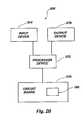
- the flip chip semiconductor device assemblyis mounted to a circuit board in a computer or a computer system.
- the circuit boardis electrically connected to a processor device which electrically communicates with an input device and an output device.
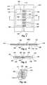
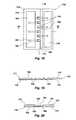
- FIG. 1is a simplified top view of an interposer substrate having recesses therein in a center row configuration according to the present invention
- FIG. 1Ais simplified bottom view of another interposer substrate design for a center row configuration according to the present invention.
- FIG. 2is a simplified cross-sectional side view taken along line 2 in FIG. 1;
- FIG. 3is a simplified cross-sectional side view take along line 3 in FIG. 1;
- FIGS. 4 A- 4 Cillustrate an interposer substrate and a method of forming recesses therein according to the present invention
- FIGS. 5 A- 5 Dillustrate another interposer substrate and a method of forming recesses therein according to the present invention
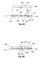
- FIGS. 6 A- 6 Billustrate a first method of mounting a semiconductor die face down to an interposer substrate in a flip chip type semiconductor assembly according to the present invention
- FIGS. 7 A- 7 Billustrate a second method of mounting a semiconductor die face down to an interposer substrate in a flip chip semiconductor device assembly according to the present invention
- FIGS. 8 A- 8 Dillustrate a third method of mounting a semiconductor die face down to an interposer substrate in a flip chip semiconductor device assembly according to the present invention
- FIGS. 9 A- 9 Billustrate a variant of the third method of mounting a semiconductor die face down to an interposer substrate in a flip chip semiconductor device assembly according to the present invention
- FIG. 10illustrates dispensing filler material through an opening in an interposer substrate in a flip chip semiconductor device assembly according to the present invention to fill recesses therein;
- FIG. 11illustrates encapsulating a semiconductor die in a flip chip semiconductor device assembly and attaching the flip chip semiconductor device assembly according to the present invention to another substrate via solder balls;
- FIG. 12illustrates a cross-sectional side view of a flip chip semiconductor device assembly including a heat transfer element according to the present invention
- FIG. 13is a simplified top view of a second embodiment of an interposer substrate having recesses therein in a center pad configuration, according to the present invention.
- FIG. 14is a simplified cross-sectional side view taken along line 14 - 14 in FIG. 13, illustrating passages between multiple openings and respective recesses in an interposer substrate, according to the present invention
- FIG. 15is a simplified cross-sectional side view take along line 15 - 15 in FIG. 13, illustrating the adhesive element on the interposer substrate and the conductive elements of the interposer substrate, according to the present invention
- FIG. 16illustrates a semiconductor die mounted face down to an interposer substrate of the second embodiment in a flip-chip type semiconductor assembly and dispensing filler material through an opening in the interposer substrate to fill recesses therein, according to the present invention
- FIG. 17illustrates encapsulating a semiconductor die in a flip chip type assembly and the flip chip type assembly attached to another, carrier substrate via solder balls, according to the present invention
- FIG. 18is a simplified top view of a third embodiment of an interposer substrate having a channel and recesses therein in a center pad configuration, according to the present invention.
- FIG. 19is a simplified cross-sectional side view taken along line 19 - 19 in FIG. 18, illustrating fingers and recesses in an interposer substrate, according to the present invention
- FIG. 20is a simplified cross-sectional side view take along line 20 - 20 in FIG. 18, illustrating the channel adjacent a recess in the interposer substrate, according to the present invention
- FIG. 21illustrates a semiconductor die mounted face down to an interposer substrate of the third embodiment in a flip chip type semiconductor assembly, according to the present invention
- FIG. 22illustrates a simplified top view of an interposer substrate of a third embodiment mounted to a semiconductor die in a flip chip type assembly and depicts dispensing filler material through an end of the channel formed in the interposer substrate to fill recesses therein, according to the present invention
- FIG. 23illustrates encapsulating a semiconductor die in a flip chip type assembly and the flip chip type semiconductor assembly attached to another substrate via solder balls, according to the present invention
- FIGS. 24 A- 24 Billustrate a method of assembling the flip chip type semiconductor assembly according to the present invention at a wafer level, wherein: FIG. 24A illustrates a wafer face down prior to being attached to an interposer substrate of the present invention; and FIG. 24B illustrates the wafer attached face down to the interposer substrate;
- FIG. 25illustrates a simplified top view of a first alternative interposer substrate having recesses therein in an I-shaped configuration, according to the present invention
- FIG. 26illustrates a simplified top view of a second alternative interposer substrate having recesses therein in a peripheral configuration, according to the present invention
- FIG. 27illustrates underfilling and encapsulating a flip chip type semiconductor assembly having the second alternative interposer substrate design, according to the present invention
- FIG. 28is a simplified block diagram of the flip chip type semiconductor assembly of the present invention integrated in a computer system.
- FIG. 29depicts an approach to implementation of the present invention using a non-flow dielectric filler material placement
- FIG. 1depicts a simplified top plan view of an interposer substrate 110 .
- the interposer substrate 110is preferably, but not limited to, a flexible substrate, which may include a dielectric substrate member 111 and a protective solder mask 118 .
- the dielectric substrate member 111may define a first surface 112 of the interposer substrate 110 and the solder mask 118 may define a second surface 114 of the interposer substrate 110 .
- the interposer substrate 110may be formed from any known substrate material and is preferably formed of, by way of example, a flexible laminated polymer or polyimide layer, such as UPILEX, produced by Ube Industries Ltd., or any other polymer-type layer.
- the interposer substrate 110may also be made of a bismaleimide triazine (BT) resin, FR 4, FR 5 or any type of substantially non-flexible material, such as a ceramic or epoxy resin.
- BTbismaleimide triazine
- the first surface 112 of interposer substrate 110includes multiple recesses or vias 120 formed therein and having mouths 120 m opening thereon to in a preselected pattern and of a predetermined size and shape.
- the multiple recesses or vias 120each include a conductive pad or terminal 122 at a bottom thereof.
- the conductive pads or terminals 122are interconnected to other conductive pads 126 on a lower surface 114 of interposer substrate 110 .
- Such conductive pads 126may be substantially directly below conductive pads or terminals 122 and merely comprise an opposing surface thereof or, more typically, the conductive pads 126 may be placed at various predetermined locations laterally offset and remote from their associated conductive pads or terminals 122 and electrically connected thereto by conductive traces 124 (shown in FIG. 1 in broken lines).
- the multiple recesses 120are formed in the interposer substrate 110 in a preselected pattern to correspond with a bond pad configuration formed on an active surface of a semiconductor die intended to be attached thereto.
- FIG. 1depicts the multiple recesses 120 in a centrally aligned, single row configuration in interposer substrate 110 .
- Such configurationis made to correspond and attach to a bumped semiconductor die having a centrally aligned, single row bond pad configuration which will be more fully illustrated hereafter.
- Other preselected patternsmay include an I-shaped recess configuration (FIG. 25) or a peripheral recess configuration (FIG.
- the present inventionmay be adapted to any recess configuration to match with a any particular, desired bond pad configuration.
- the multiple recesses 120may be formed in any suitable shape, such as square, rectangular and circular, and may include tapered side walls so that the openings or mouths of the recesses 120 are larger than the bottoms thereof.
- Conductive pads or terminals 122may completely cover the bottoms of recesses 120 or, as depicted in FIG. 1, may be narrower than recesses 120 at the bottoms thereof so that gaps 121 are defined on one or both sides of conductive pads or terminals 122 .
- the conductive traceswhich may, for example, comprise copper or a copper alloy, may be adhered to the dielectric substrate member of UPILEX, BT resin, FR 4 or, FR 5 laminate material, or other substrate materials, using adhesives as known in the art.
- the material of the conductive tracesmay be adhesively laminated to the substrate in the form of a conductive sheet, the traces then being subtractively formed from the conductive sheet, as by etching.
- interposer substrate 110may also include an opening 130 (shown in broken lines) formed in there across, the opening 130 substantially extending along a longitudinal extent of the centrally aligned, single row configuration of the multiple recesses 120 from one end of interposer substrate 110 to the other.
- Opening 130may be formed wholly in the material of dielectric substrate member 111 , or may, as shown by the broken lead line from reference numeral 130 in FIG. 2 and the broken lines and the broken lead line from reference numeral 130 in FIG. 3, be formed in solder mask 118 .
- opening 130may be formed partially in dielectric member 111 and partially solder mask 118 , as desired.
- Opening 130may be formed to align along any employed recess configuration, i.e., I-shape, peripheral.
- FIG. 2depicts a cross-sectional view taken along lines 2 - 2 in FIG. 1.
- opening 130includes multiple segments 132 , each segment 132 extending between separate individual recesses 120 of the multiple recesses 120 .
- each segment 132 as shownextends along the axis of opening 130 to a side portion of each of the recesses 120 ; however the segments 132 may extend and be positioned from the opening 130 to the recesses 120 in any suitable manner. For example, and as depicted in FIG.
- opening 130may comprise a slot laterally offset from recesses 120 which are themselves defined between fingers 111 f of flexible dielectric member 111 which terminate at opening 130 .
- conductive traces 124extend across opening 130
- solder mask 118covers the end portions thereof flanking opening 130 and providing an enhanced depth and width to opening 130 for underfilling purposes.
- FIG. 3is a cross-sectional view taken along lines 3 - 3 of FIG. 1.
- FIG. 3depicts opening 130 extending directly into the recesses 120 , i.e., into the plane of the drawing sheet. Such opening 130 is shown as having a lateral width smaller than the recesses 120 , however, the opening may by sized substantially equal to, or larger than, the lateral width of the recesses 120 .
- FIG. 3also depicts conductive pads or terminals 122 at the bottom of each of the recesses 120 interconnected through conductive traces 124 with conductive pads 126 exposed at the lower surface 114 of the interposer substrate 110 through solder mask 118 .
- FIGS. 1 and 3also depict an adhesive element 116 disposed on the first surface 112 of the interposer substrate 110 .
- adhesive element 116is preferably disposed on a portion of the first surface 112 of the interposer substrate 110 that is adjacent but separated from each of the multiple recesses 120 .
- the adhesive element 116may be any suitable adhesive material as known in the art, such as an epoxy, acrylic, or other suitable adhesive.
- the adhesive element 116may comprise, without limitation, a polyimide tape bearing adhesive on both sides thereof with the exposed surface (facing away from dielectric substrate member 111 ) being covered with a protective release layer until adherence to a semiconductor die is required.
- Such adhesive element 116is preferably, but not limited to, of a maximum 25 ⁇ m thickness.
- adhesive elementmay be employed to function as a spacer between a semiconductor die and interposer substrate 110 to provide a vertical standoff therebetween or to control the degree of insertion of conductive bumps carried by the semiconductor die into recesses 120 .
- FIG. 4Adepicts interposer substrate 110 including a dielectric substrate member 111 having a bottom conductive layer formed on a surface thereof and a protective solder mask 118 formed over the conductive layer.
- the dielectric substrate member 111is preferably a flexible material, such as the above-described flexible laminated polymer material or polyimide layer, but may also include a substantially non-flexible material.
- the bottom conductive layeris preferably copper, or a copper alloy, but may be any suitable electrically conductive material.
- the bottom conductive layermay comprise conductive traces 124 extending between conductive pads or terminals 122 and conductive pads 126 (see FIG. 3).
- Such conductive traces 124may be formed by masking and etching a bottom metal or alloy conductive layer or, alternatively, the traces 124 may be formed by printing using conductive ink, or otherwise formed using any method known in the art. Once the conductive traces 124 are patterned, the protective solder mask 118 may be formed thereover.
- FIG. 4Bdepicts dielectric substrate member 111 with one of the recesses 120 formed therein.
- Such recesses 120may be formed by patterning, utilizing a chemical wet etch or dry etch, mechanical drilling or punching, laser ablation, by any method known in the art and suitable for use with the type of material employed for the dielectric substrate member 111 .
- the recesses 120are preferably formed to expose portions of one of the traces 124 , such as conductive pads or terminals 122 .
- each recess 120may include a conductive layer 123 thereon formed, for example, by electroless plating; however, such plating is not required for practice of the present invention.
- recessesmay be formed with large mouths 120 m which taper to a smaller bottom 120 b. Such tapering may be easily effected using isotropic etching techniques as known in the art.
- FIGS. 5A through 5Ddepicts a process similar to that depicted and described in FIGS. 4 A- 4 C of forming recesses 120 in the first surface 112 of interposer substrate 110 , with the additional of another layer, namely an second conductive layer 125 , as shown in FIG. 5A.
- second conductive layer 125is preferably a copper or copper alloy layer, but may be any suitable electrically conductive material, and may be patterned with traces depending on the needs and requirements of the particular semiconductor die to which the interposer substrate 110 is attached.
- FIG. 5Bdepicts upper conductive layer 125 patterned to expose portions of dielectric substrate member 111 where the recesses 120 are to be formed and substantially etched back from the intended lateral boundaries of the recess mouths.
- a recess 120is then formed in the exposed portions of substrate member 111 , by a chemical wet etch or dry etch, mechanical drilling or punching or laser ablation; however, the recess 120 may be formed utilizing any method known in the art and suitable with the type of material employed for the interposer substrate 110 .
- the recesses 120are preferably formed to expose conductive pads or terminals 122 of the conductive traces 124 , after which additional conductive material may be placed over the exposed portion of the conductive pads or terminals 122
- a conductive layer 121may be formed by electroless plating on the walls of the recesses 120 so that such conductive layer 121 contacts a portion of the conductive pads or terminals 122 of the exposed traces 124 , as depicted in FIG. 5D. As shown in FIGS.
- solder mask 118may provide full coverage over the bottoms of conductive traces 124 or, as shown in broken lines, may include an aperture or apertures therethrough, for example to provide an opening 130 , to expose the undersides of conductive traces 124 at the locations of recesses 120 or otherwise, as desired, for enhanced underfill access. If a wet solder mask 118 is employed, recesses 120 in dielectric member 111 are plugged with a removable material before solder mask application; if a dry (film) solder mask 118 is employed, it may merely be laminated to dielectric member 111 .
- FIGS. 6 A- 6 Bdepict simplified cross-sectional views of a first method of mounting and bonding interposer substrate 110 to a semiconductor die 150 in a flip chip type semiconductor device assembly 160 .
- FIG. 6Aillustrates the first surface 112 of interposer substrate 110 aligned and facing the semiconductor die 150 prior to the assembly thereof.
- Semiconductor die 150includes an active surface 152 and a back side or surface 154 , wherein the active surface 152 includes a plurality of bond pads 158 bearing electrically conductive bumps 156 thereon.
- Such conductive bumps 156 and bond pads 158 of semiconductor die 150are of a preselected configuration, wherein the recesses 120 in interposer substrate 110 are sized and configured to correspond with the configuration of the bond pads 158 and conductive bumps 156 of semiconductor die 150 so that the respective configurations or patterns of recesses 120 and conductive bumps 156 are substantially mirror images of each other.
- solder mask 118may have an opening 130 defined therethrough or, alternatively, full solder mask coverage may be provided across the bottoms of conductive traces, including the locations of recesses 120 as previously described with respect to FIGS. 5A through 5D.
- Conductive bumps 156preferably comprise, but are not limited to, conductive balls, pillars or columns.
- the material of conductive bumps 156may include, but is not limited to, any known suitable metals or alloys thereof, such as lead, tin, copper, silver or gold. Conductive or conductor-filled polymers may also be employed, although gold and PbSn solder bumps are currently preferred.
- the conductive bumps 156may be of uniform characteristics throughout or include, for example, a core of a first material (including a nonconductive material) having one or more conductive layers of other materials thereon.
- Conductive bumps 156are preferably formed on the active surface 152 of each semiconductor die 150 at a wafer level, but such is not required. Conductive bumps 156 may be formed by metal evaporation, electroplating, stencil printing, gold stud bumping by wire bonders, or any suitable method known in the art.
- FIG. 6Bdepicts interposer substrate 110 mounted to semiconductor die 150 to form flip chip semiconductor device assembly 160 , wherein such assembly 160 provides that each of the conductive bumps 156 are substantially inserted in a corresponding recess 120 of interposer substrate 110 and engage with the conductive pads or terminals 122 at the bottom of each of the recesses 120 .
- Such assembly 160may be initially attached by the adhesive 116 carried on the first surface 112 of the interposer substrate 110 .
- the conductive bumps 156 on the semiconductor die 150may then be bonded to the conductive pads or terminals 122 in the recesses 120 of interposer substrate 110 by, for example, reflowing the bumps 156 (in the case of solder bumps) or curing the bumps 156 (in the case of conductive or conductor filled polymer bumps) as known in the art. Other methods of bonding known in the art may utilized, such as ultrasonic or thermal compression.
- FIGS. 7 A- 7 Bdepict simplified cross-sectional views of a second method of mounting and bonding interposer substrate 110 to a semiconductor die 150 in a flip chip semiconductor device assembly 160 .
- FIG. 7Aillustrates the first surface 112 of interposer substrate 110 aligned with and facing the semiconductor die 150 prior to the assembly thereof.
- FIG. 7Ais similar to FIG. 6A in substantially every respect, except the conductive bumps 156 on the semiconductor die 150 carry a conductive paste 182 thereon.
- Such conductive paste 182may be provided on the bumps by dipping the bumps 150 into a pool of conductive paste 182 or by depositing, dispensing or otherwise transferring the conductive paste 182 to the conductive bumps 150 .
- the conductive paste 182may include, but is not limited to, eutectic solder, conductive epoxy, or any non-solid conductive material known in the art.
- solder mask 118may have an opening 130 defined therethrough or, alternatively, full solder mask coverage may be provided across the bottoms of conductive traces, including the locations of recesses 120 as previously described with respect to FIGS. 5A through 5D.
- the interposer substrate 110is mounted to semiconductor die 150 to form semiconductor device assembly 160 , wherein each of the conductive bumps 156 are substantially inserted into corresponding recesses 120 of interposer substrate 110 with the conductive paste 182 engaging with the conductive pads or terminals 122 in each of the recesses 120 .
- the conductive paste 182provides contact with the conductive pads or terminals 122 even if some of the conductive bumps 156 are inconsistent in height, i.e., their free ends are non-coplanar.
- Such conductive bumps 156 having the conductive paste provided thereonmay then be bonded to the conductive pads or terminals 122 in the recesses 120 of interposer substrate 110 as previously described in association with FIGS. 6A and 6B.
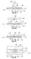
- FIGS. 8 A- 8 Ddepict simplified cross-sectional views of a third method of preparing, mounting and bonding interposer substrate 110 with a semiconductor die 150 in a flip chip type semiconductor device assembly 160 .
- FIG. 8Adepicts interposer substrate 110 having a mass of conductive paste 182 disposed over a stencil 186 , patterned with openings which correspond with recesses 120 .
- the conductive paste 182is then spread by a spreading member 184 over the stencil 186 so that the conductive paste 182 is deposited in each of the recesses 120 .
- the stencil 186is then removed prior to aligning the conductive bumps 156 on the semiconductor die 150 with the recesses 120 in the interposer substrate 110 , as depicted in FIG. 8B.
- conductive paste 182may be disposed into recesses 120 without using a stencil 186 , using the surface of dielectric member 111 itself as a stencil.
- FIG. 8Cdepicts the interposer substrate 110 mounted to semiconductor die 150 to form semiconductor device assembly 160 , wherein each of the conductive bumps 156 are substantially inserted into the conductive paste 182 in the corresponding recesses 120 of interposer substrate 110 .
- the conductive paste 182provides electrical and mechanical interconnection between the bond pads 122 or trace ends and the conductive bumps 150 even if some of the conductive bumps 156 are inconsistent in height, i.e., their free ends are non-coplanar.
- the semiconductor die 150may then be bonded with the interposer substrate 110 as previously described in association with FIGS. 6A and 6B.
- stencil 186may not be required if the mass of conductive paste 182 is disposed and spread into recesses 120 prior to disposition of an adhesive element 116 over first surface 112 .
- conductive paste 182if eutectic solder, may be disposed in recesses 120 and then reflowed and solidified prior to attachment of semiconductor die 150 to interposer substrate 110 using a second reflow to provide an indefinite shelf life for interposer substrate 110 .
- semiconductor die 150may be aligned with interposer substrate 110 after conductive paste disposition and a single reflow employed.
- 8Dis an enlarged view of a single conductive bump 156 carried by a semiconductor die 150 in initial contact with a mass of conductive paste 182 disposed in a recess 120 in dielectric member 111 of interposer substrate 110 over conductive pad or terminal 122 of a conductive trace 124 .
- a conductive bump 156to be used either in cooperation with or in lieu of a conductive bump 156 carried by semiconductor die 150 may be formed in each of recesses 120 through plating of conductive pads or terminals 120 with a conductive material such as a suitable metal. Such plating may be effected electrolytically, using a bus line connected to each conductive trace 124 , or by electroless plating, both techniques being well known in the art.
- FIGS. 9 A- 9 Bdepict simplified cross-sectional views of a variant of the above-described third method comprising a fourth method of preparing, mounting and bonding interposer substrate 110 to a semiconductor die 150 in a flip chip semiconductor device assembly 160 .
- Such variantis similar to the third method as described in FIGS. 8 A- 8 C of providing conductive paste in each of the recesses 120 , except the conductive bumps 156 are initially unattached to the bond pads 158 of the semiconductor die 150 .
- the conductive bumps 156 in the form of balls, such as metal balls,are embedded into the conductive paste 182 which was previously spread into the recesses 120 of the interposer substrate 110 .
- the bond pads 158 in the semiconductor die 150are aligned with the conductive bumps 156 in the recesses 120 in the interposer substrate 110 and then mounted thereto, as depicted in FIGS. 9 A- 9 B.
- the conductive paste 182may comprise a solder wettable to both bond pads 158 and conductive pads or terminals 122 or a conductive or conductor-filled adhesive. It will also be understood and appreciated that conductive bumps 156 may themselves comprise solder, such as a PbSn solder, and conductive paste 182 eliminated or also comprising a compatible solder.
- a conductive bump 156 to be used in lieu of a conductive bump 156 carried by semiconductor die 150may be formed in each of recesses 120 through plating of conductive pads or terminals 120 with a conductive material such as a suitable metal.
- conductive bumps 156may be formed larger in size than those of conventional flip chip assemblies without increasing, or even while decreasing, the height of the flip chip semiconductor device assembly 160 , resulting in the increase in electrical and mechanical reliability and performance of the interconnections between the interposer substrate 110 and the semiconductor die 150 .
- the recesses 120 in the interposer substrate 110provide an inherent alignment aspect absent in a conventional flip chip semiconductor device assembly because the conductive bumps 156 easily slide into their respective corresponding recesses 120 to ensure proper alignment and proper attachment thereof.
- the adhesive element 116 on the first surface 112 of the interposer substrate 110 as well as the conductive paste 182 in the recesses 120may act as a height controller for reliable attachment of the semiconductor die 150 to the interposer substrate 110 , wherein the adhesive element 116 and/or the conductive paste 182 may be used to compensate for any irregularities due to varied conductive bump sizes, recess depths and planarity variation in the surfaces of the interposer substrate 110 and semiconductor die 150 .
- a dielectric filler material 166(commonly termed an “underfill” material) maybe optionally applied through opening 130 .
- the method employed to apply the filler material 166is preferably by dispensing under pressure from dispenser head 164 , but may include any method known in the art, such as gravity and vacuum injecting. In this manner, the dielectric filler material 166 may be applied into the opening 130 , move as a flow front through the multiple passages 132 and into each of the recesses 120 to fill a space around the conductive bumps 156 , bond pads 158 and conductive pads or terminals 122 .
- the dielectric filler material 166may be self-curing through a chemical reaction, or a cure accelerated by heat, ultraviolet light or other radiation, or other suitable means in order to form at least a semisolid mass in the recesses 120 .
- Such dielectric filler material 166provides enhanced securement of the components of flip chip semiconductor device assembly 160 as well as precluding shorting between conductive elements and protecting the conductive elements from environmental concerns, such as moisture.
- the semiconductor assembly 160 of the present inventionrequires less time since the filler material may only be directed to fill the recesses 120 or, rather, any left over space within in the recesses 122 proximate the interconnections, i.e., bumps 156 .
- the interposer substrate 110 described for use in such methodsmay not include an opening for applying filler material to the recesses 120 because the recesses 120 are substantially filled with conductive paste 182 . Therefore, it is contemplated that applying filler material through an opening 130 in the interposer substrate 110 described in the third and fourth methods may not be necessary.
- FIG. 10also depicts conductive balls 162 , such as solder balls or any suitable conductive material 162 , provided at the conductive pads 126 exposed at the second surface 114 of the interposer substrate 110 .
- conductive balls 162may be provided prior to or subsequent to dispensing the filler material 166 , and formation thereof, if formed of solder, is facilitated by solder mask 118 (see FIG. 2) and apertures therethrough placed over locations of conductive pads 126 .
- conductive balls 162may comprise other materials, such as conductive epoxies or conductor-filled epoxies, and may comprise other shapes, such as bumps, columns and pillars.
- the semiconductor die 150may then be either partially or fully encapsulated by an encapsulation apparatus 178 with a dielectric encapsulation material 168 as depicted in FIG. 11.
- encapsulation material 168may be dispensed by dispenser head 164 about the periphery of the die 150 so that the back side or surface 154 of the die is left exposed.
- encapsulation material 168may be provided by dispensing, spin-coating, glob-top, pot molding, transfer molding, or any suitable method known in the art. It is currently preferred that such encapsulation material 168 be applied to the backside or surface 154 of the semiconductor die 150 (which may include at the wafer level, as by spin-coating) prior to dispensing additional encapsulation material 168 about the periphery of the semiconductor die 150 in order to facilitate fully encapsulating the die 150 .
- FIG. 11also depicts flip chip semiconductor device assembly 160 attached to another carrier substrate 170 , such as a printed circuit board or mother board.
- the carrier substrate 170includes a substrate upper surface 172 and a substrate lower surface 174 , upper surface 172 bearing substrate terminal pads 176 arranged to correspond and attach with conductive balls 162 on the bottom surface 114 of interposer substrate 110 .
- the flip chip semiconductor device assembly 160may be mechanically and electrically connected to substrate 170 by reflowing the conductive (solder) balls 162 to the substrate pads 176 .
- a dielectric filler material(not shown) as known in the art may then be applied between the flip chip semiconductor device assembly 160 and the carrier substrate 170 for securing and protecting the interconnections, i.e., conductive balls 162 , therebetween.
- FIG. 12depicts a flip chip semiconductor device assembly 160 including a heat transfer element 180 .
- the heat transfer element 180may be provided over the first surface 112 of the interposer substrate 110 and under the adhesive 116 as a thin, thermally conductive material.
- the heat transfer element 180may also be provided on the active surface 152 of the semiconductor die 150 to abut the first surface 112 of the interposer substrate 110 .
- Another optionis to provide the heat transfer element 180 on the back surface 154 of the semiconductor die 150 as shown in broken lines.
- Such heat transfer device element 180is configured and located to thermally conduct heat formed and generated from the electrical components of the semiconductor die 150 and to remove such heat from the flip chip semiconductor device assembly 160 , to reduce the incidence of thermal fatigue in the interconnections and circuitry of the assembly 160 and, specifically, the semiconductor die 150 as well as reducing operating temperatures.
- the heat transfer element 180maybe formed of any thermally conductive material, such as copper and silver, but may also comprise a thermally conductive material that is non-electrically conductive, such as a thin diamond material and/or diamond composite deposited as a thin film or layer.
- FIG. 13depicts a top plan view of a second embodiment of an interposer substrate 610 having a center recess configuration.
- the second embodimentis similar to the first embodiment in most respects, except the interposer substrate 610 of the second embodiment includes multiple openings 630 through dielectric layer 611 .
- interposer substrate 630includes a first surface 612 and a second surface 614 , wherein the upper surface 612 includes multiple recesses 620 therein and bears one ore more adhesive elements 616 .
- FIGS. 14 and 15depict cross-sectional views of interposer substrate 610 taken along respective section lines 14 and 15 in FIG. 13, illustrating the multiple openings 630 formed in the solder mask 618 aligned with second surface 614 of interposer substrate 610 and each of the openings 630 extending to a corresponding one of the multiple recesses 620 .
- Each opening 630 and recess 620extends to a conductive element such as a conductive trace 624 or conductive pad or terminal 622 with one or more passages 632 comprising gaps between a conductive pad or terminal 622 or conductive trace 624 providing communication between each opening 630 and recess 620 .
- the one or more passages 632may extend from an upper portion of each opening 630 to a bottom portion of each recess 620 in the interposer substrate 610 .
- the conductive traces 624 or conductive pads or terminals 622 as shown in FIG. 13are suspended and extend across an upper portion of each opening 630 and a lower portion of each recess 620 , of which each conductive trace 624 may extend to another portion of the interposer substrate 610 to conductive pads 626 for electrical interconnection on a lower surface 614 of interposer substrate 610 .
- Such bond conductive pads 626may be located substantially directly below conductive pads 622 or routed laterally across interposer substrate 610 to various predetermined locations by the conductive traces 624 .
- Solder mask 618also includes apertures therethrough at the locations of conductive pads 626 on which discrete conductive elements in the form of solder balls may be formed for external electrical connection of interposer substrate 610 .
- FIG. 16depicts the interposer substrate 610 of the second embodiment mounted and bonded to a semiconductor die 650 having conductive bumps 656 on an active surface 652 thereof to provide a, flip chip semiconductor device assembly 660 .
- the conductive bumps 656are arranged in a mirror image of the recess configuration in the interposer substrate 610 so that the die 650 and interposer substrate 610 are attached with the conductive bumps 656 disposed in each of the recesses 620 and the conductive bumps 656 electrically connected to the conductive pads or terminals 622 or trace ends either directly or via a conductive solder paste or other non-solid conductive material.
- the one or more passages 632allow dielectric filler material 166 to flow therethrough into each of the recesses 620 from a dispenser 164 positioned proximate and facing each of the openings 630 .
- Dispenser 164may introduce dielectric filler material 166 under pressure into openings 630 to be extruded through passages 632 into recesses 620 adjacent conductive bumps 656
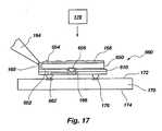
- the semiconductor die 650 in the flip chip semiconductor device assembly 660 of the second embodimentmay then be either fully encapsulated or partially encapsulated by encapsulation member 178 with an encapsulation material 168 as depicted in FIG. 17.
- encapsulation material 168may be dispensed by dispenser 164 about the periphery of the die 650 so that the back surface 654 of the die is left exposed.
- encapsulation material 168may be applied to the back surface 654 of the semiconductor die 650 (which may include at the wafer level) prior to dispensing encapsulation material 168 about the periphery of the die 650 in order to facilitate fully encapsulating the die 650 .
- FIG. 17also depicts semiconductor assembly 660 attached to another substrate 170 , such as a printed circuit board or mother board.
- the substrate 170includes a substrate upper surface 172 and a substrate lower surface 174 with substrate pads 176 made to correspond and attach with conductive balls 662 , such as solder balls, on the bottom surface 614 of interposer substrate 610 .
- Conductive balls 662if solder, may be formed by placement of solder paste on conductive pads 626 followed by reflow, preformed and secured to conductive pads 626 , applied to substrate pads 176 , or otherwise as known in the art.
- the semiconductor assembly 660may be bonded to substrate 170 by reflowing the conductive balls 662 to the substrate pads 176 .
- a dielectric filler material(not shown) may then be applied between the semiconductor assembly 660 and the substrate 170 for securing and protecting the interconnections, i.e., conductive balls 662 , therebetween.
- FIG. 18depicts a top plan view of a third embodiment of an interposer substrate 710 having a center recess configuration.
- the interposer substrate 710 of the third embodimentis similar to the first embodiment, except the interposer substrate 710 of the third embodiment does not include openings extending to recesses 720 at a second surface 714 of interposer substrate 710 .
- First surface 712carries one or more adhesive elements 716 thereon.
- Second surface 714carries a plurality of conductive elements in the form of conductive pads or terminals 722 and conductive traces 724 which may have associated therewith conductive pads 726 for formation of discrete conductive elements thereon for connecting interposer substrate 710 to external circuitry.
- Solder mask 718may be employed to dam the bottoms of recesses 720 as well as the bottom of channel 740 .
- channel 740may be of lesser depth than recesses 720 and not extend all the way through dielectric layer 711 .
- FIGS. 18 - 20depict a channel 740 formed in a first surface 712 of interposer substrate 710 , wherein FIGS. 19 and 20 depict cross-sectional views of interposer substrate 710 taken along respective section lines 19 and 20 in FIG. 18.
- the channel 740may, but is not limited to, extend to a depth substantially the same as the recesses 720 and is configured to extend longitudinally alongside the row of recesses 720 so that each recess 720 may directly communicate with the channel 740 .
- a portion of the interposer substrate 710 between each recess 720comprises alignment fingers 742 , which are defined by forming the recesses 720 and the channel 740 therealong in interposer substrate 710 .
- alignment fingers 742provide an alignment characteristic so that the conductive bumps may be positioned and aligned with the conductive pads or terminals 722 when being disposed in the recesses 720 .
- a semiconductor die 750may be mounted and bonded to interposer substrate 710 so that the active surface 752 of the semiconductor die 750 abuts with the upper surface 712 of the interposer substrate 710 and the conductive bumps 756 are disposed in the recesses 756 to form a semiconductor assembly 760 , as described in the previous embodiments.
- FIG. 22depicts the channel 740 having a channel opening 744 at a side periphery of the assembly 760 , through which dielectric filler material 166 may be introduced.
- Such filler materialmay be dispensed from dispenser 164 proximate the channel opening 744 , wherein dielectric filler material 166 may flow and fill in spaces around the conductive bumps 756 in the recesses 720 .
- Such processmay be employed with the semiconductor assembly 760 horizontal, vertical, or at any angle which may promote the filler material to fill the recesses 720 .
- the dielectric filler material 166 introductionmay also be enhanced by a vacuum or suction means to optimize the time it takes to fill in the recesses 720 .
- each conductive pad or terminalmay be provided with a hole therethrough through which air may be expelled by the flow front F of dielectric filler material 166 or to which a vacuum may be applied.
- semiconductor die 750may be fully encapsulated with encapsulation member 178 and dispenser 164 or partially encapsulated with dispenser 164 , as depicted in FIG. 23.
- FIG. 23also depicts semiconductor assembly 760 attached to another substrate 170 , such as a printed circuit board or mother board.
- the substrate 170includes a substrate upper surface 172 and a substrate lower surface 174 with substrate pads 176 made to correspond and attach with conductive balls 762 , such as solder balls, on the bottom surface 714 of interposer substrate 710 .
- the semiconductor assembly 760may be bonded to substrate 170 by reflowing the conductive balls 762 to the substrate pads 176 .
- a filler material(not shown) may then be applied between the semiconductor assembly 760 and the substrate 170 for securing and protecting the interconnections, i.e., conductive balls 762 , therebetween.
- the interposer substrate 110 of the present inventionmay also be formed initially on a wafer scale corresponding to a semiconductor wafer carrying a plurality of unsingulated semiconductor dice 150 and then singulated or separated after assembly by a dicing process into the individual flip chip semiconductor device assemblies 160 .
- the term “wafer”not limited to conventional substantially circular semiconductor wafers but extends to any large scale substrate including a layer of semiconductor material of sufficient size for formation of multiple dice thereon and encompasses portions of such large scale substrates bearing multiple semiconductor dice.
- FIG. 24Adepicts a simplified cross-sectional view of a semiconductor wafer 250 facing a wafer scale interposer substrate 210 prior to mutual attachment thereof.
- the semiconductor wafer 250collectively includes multiple semiconductor dice 251 in columns and rows separable along borders 253 as shown in broken lines, wherein the wafer 250 includes a back side or surface 254 and an active surface 252 and each semiconductor die 250 includes conductive bumps 256 in a configuration dictated by the bond pads 258 on which they are formed.
- the interposer substrate 210includes a first surface 212 and a second surface 214 with multiple recesses 220 formed in the first surface 212 and openings 230 having passages (not shown) formed in the second surface 214 .
- the recesses 220 formed in the interposer substrate 210are made to correspond in substantially a mirror image with the bump configuration on each of the dice 251 of the wafer 250 .
- the interposer substrate 210may be attached to the wafer 250 via an adhesive element 216 on the first surface 212 of the interposer substrate 2 10 so that the bumps 256 on the wafer 250 are inserted into and substantially received within the multiple recesses 220 formed in the interposer substrate 210 to form a wafer scale assembly 260 , as depicted in FIG. 13B.
- the wafer assembly 260may then be singulated or “diced” along the borders 253 of the wafer 250 via a dicing member such as a wafer saw 280 to form individual, singulated flip chip semiconductor device assemblies that each include one or more semiconductor die 251 having the separated interposer substrate 210 of the present invention mounted thereon.
- the conductive bumps 256may be bonded to the conductive pads or terminals in the recesses 220 to, therefore, mechanically bond and electrically connect the semiconductor wafer 250 to the wafer scale interposer substrate 210 .
- dielectric filler materialmay be applied through the openings 230 and conductive balls 262 may be provided on the bond posts on the second surface 214 of the interposer substrate 210 , either prior to dicing the wafer scale assembly 260 or subsequent thereto.
- FIG. 25depicts a top plan view of an interposer substrate 310 having an alternative recess configuration made for corresponding to a substantial “mirror image” bond pad configuration on the active surface of a semiconductor die.
- this first alternativethere is an I-shaped bond pad configuration, wherein multiple recesses 320 are formed over the upper surface 312 of interposer substrate 310 that are aligned in the shape of an “I” with adhesive elements 316 disposed on either side of the body of the “I” and between the ends thereof.
- the recessesmay be formed in an interposer substrate around a periphery thereof. Such alternative is depicted in FIG.
- interposer substrate 410with an adhesive element 416 at a center portion of interposer substrate 410 and recesses 420 formed thereabout and proximate a periphery of interposer substrate 410 .
- the periphery recess configuration in interposer substrate 410is made to correspond with a substantial “mirror image” bond pad configuration on an active surface of a semiconductor die.
- both the I-shaped and the periphery configurations depicted in FIGS. 25 and 26may include one or more openings in a surface of the interposer substrate opposing that through which the recesses are formed with passages extending therefrom to each of the recesses.
- dielectric filler materialmay be applied through the opening and passages to fill the recesses and protect the conductive bumps disposed therein.
- FIG. 27depicts a cross-sectional view of a semiconductor assembly 460 including a semiconductor die 450 mounted face down to an interposer substrate 410 having a peripheral recess configuration and an alternative method of applying dielectric filler material 166 to the assembly 460 .
- dielectric filler material 166may be applied by dispenser 164 around the periphery of the semiconductor die 450 so that the dielectric filler material 166 flows under the die 450 and around the conductive bumps 456 adjacent the die periphery. As such, the dielectric filler material 166 is only needed proximate the conductive bumps 456 and not under the entire die as done conventionally.
- the semiconductor die 450may be left exposed or be encapsulated by encapsulation member 178 , which may provide encapsulation material 168 to the assembly 460 via dispensing, spin-coating, glob-top, depositing or transfer molding, or any suitable method known in the art. It is preferred that such encapsulation material 168 be applied to the back surface 454 of the semiconductor die 450 at the wafer level or prior to dispensing the filler material 162 about the periphery, to facilitate fully encapsulating the die 450 .
- the semiconductor die 450is assembled and bonded to the interposer substrate 410 with the conductive bumps 456 disposed in the conductive paste 182 as described in FIGS. 8 A- 8 C and 9 A- 9 B; however, this alternative may also employ the methods described in FIGS. 6 A- 6 B and 7 A- 7 B for assembling and bonding the die 450 to the interposer substrate 410 .
- flip chip semiconductor device assembly 160 of the present inventionis mounted to a circuit board 570 , such as previously-discussed carrier substrate 170 , in a computer system 500 .
- the circuit board 570is connected to a processor device 572 which communicates with an input device 574 and an output device 576 .
- the input device 574may be a keyboard, mouse, joystick or any other computer input device.
- the output device 576may be a monitor, printer or storage device, such as a disk drive, or any other output device.
- the processor device 572may be, but is not limited to, a microprocessor or a circuit card including hardware for processing computer instructions. Additional structure for the computer system 500 is readily apparent to those of ordinary skill in the art.
- an interposer substrate 110may be provided having conductive traces 124 laminated thereto, the bottoms thereof being fully covered or, optionally, uncovered, by solder mask 118 , and a conductive bump 156 a formed by reflow (if solder) or curing (if an epoxy) of a mass of conductive paste 182 at the bottom of each recess 120 .
- a dielectric filler material 166in then disposed over conductive bumps 156 a in each recess 120 as shown.
- Adhesive elements 116may, as shown, be used, or may be omitted, as desired.
- a nonconductive film NCF as shown in broken lines in FIG. 29be disposed over interposer substrate 110 after formation of conductive bumps 156 a thereon and prior to assembly with a semiconductor die 150 carrying conductive bumps 156 b.
- bumps 156 a and 156 bwill penetrate the nonconductive film to initiate mutual electrical contact therebetween.
- Suitable nonconductive filmsinclude the UF511 and UF527 films offered by Hitachi Chemical, Semiconductor Material Division, Japan.
- the flip chip semiconductor device assembly of the present inventionprovides a compact, robust package at a reduced cost in comparison to conventional bumped semiconductor die assemblies employing dual conductive layer interposers.
- a package height reduction of about 90 ⁇ mmay be effected using a 100 ⁇ m thick dielectric member and eliminating a second 12 ⁇ m thick conductive layer adjacent the semiconductor die, even with a 25 ⁇ m thick adhesive element comprising a tape disposed between the semiconductor die and interposer substrate, since the discrete conductive elements or conductive bumps of the die may be substantially completely received within the recesses of the dielectric member, but for any vertical standoff provided by the tape.
- the present inventionmay employ a recess lateral dimension or diameter which is far in excess of the lateral dimension or diameter of an associated conductive bump, thus greatly facilitating bump and recess alignment by loosening required dimensional tolerances.
- a 75 ⁇ m bumpmay be employed with a 120 ⁇ m recess using a 175 ⁇ m pitch
- a flexible interposer substrateeasily accommodates minor variations between heights of various conductive bumps and lack of absolute planarity of the semiconductor die active surface as well as that of the terminals. Further, encapsulation, if desired, of some or all portions of the periphery and back surface of the semiconductor die by a variety of methods is greatly facilitated, as is incorporation of a thermally conductive heat transfer element such as a heat sink without adding complexity to the package. If an adhesive element employing a tape is used to secure the semiconductor die and interposer substrate together, different bond pad arrangements are easily accommodated without the use of a liquid or gel adhesive and attendant complexity of disposition.
- tapemay be used to resolve lack of coplanarity of the conductive bumps on a semiconductor die or at wafer level and to provide cushioning during die attach to the interposer substrate, as force may be applied sufficient to ensure contact of the conductive bumps with terminals without damage to the assembly. More specifically, during semiconductor die placement, the tape may act as a stopper or barrier, and as a cushion. If a conductive paste is deposited in a via, the tape acts as a barrier to prevent paste contamination of the surface of the semiconductor die. If, on the other hand, solidified conductive bumps, when heat is used to soften the bump material, the tape acts as a stopper as well as a cushion when the bump material relaxes. In addition, tape accommodates the “spring back” effect exhibited when force used to assemble a semiconductor die and interposer substrate is released, helping to keep the interconnection or joint together.
- tapefacilitates handling of the assembly prior to reflow of solder-type conductive bumps in the recesses as well as rework, as the assemblies may be electrically tested before reflow and before a dielectric filler is applied and/or the semiconductor die encapsulated and a defective die removed and replaced.
- the presence of the tapealso reduces the volume of dielectric filler material (if employed) required between the interposer substrate and semiconductor die and its compliant characteristics reduce the potential incidence of stress-induced defects due to thermal cycling of the assembly during operation.
Landscapes
- Engineering & Computer Science (AREA)
- Microelectronics & Electronic Packaging (AREA)
- Computer Hardware Design (AREA)
- Power Engineering (AREA)
- Physics & Mathematics (AREA)
- Condensed Matter Physics & Semiconductors (AREA)
- General Physics & Mathematics (AREA)
- Manufacturing & Machinery (AREA)
- Wire Bonding (AREA)
Abstract
Description
- This application is related to U.S. patent application Ser. No. 09/944,465 filed Aug. 30, 2001 and entitled MICROELECTRONIC DEVICES AND METHODS OF MANUFACTURE, and to the following U.S. patent applications filed on even date herewith: Serial No. (Attorney Docket No. 4812US), entitled INTERPOSER CONFIGURED TO REDUCE THE PROFILES OF SEMICONDUCTOR DEVICE ASSEMBLIES AND PACKAGES INCLUDING THE SAME AND METHODS; Serial No. (Attorney Docket No. 4877US), entitled METHOD AND APPARATUS FOR FLIP-CHIP PACKAGING PROVIDING TESTING CAPABILITY; Serial No. (Attorney Docket No. 4878US), entitled SEMICONDUCTOR DIE PACKAGES WITH RECESSED INTERCONNECTING STRUCTURES AND METHODS FOR ASSEMBLING THE SAME; Serial No. (Attorney Docket No. 4879US), entitled FLIP CHIP PACKAGING USING RECESSED INTERPOSER TERMINALS; and Serial No. (Attorney Docket No. 4974US), entitled METHODS FOR ASSEMBLY AND PACKAGING OF FLIP CHIP CONFIGURED DICE WITH INTERPOSER.[0001]
- 1. Field of the Invention[0002]
- The present invention relates to methods and apparatus for assembling and packaging single and multiple semiconductor dice with an interposer substrate. In particular, the present invention relates to methods and apparatus for underfilling single and multiple semiconductor dice assembled in a flip chip orientation with an interposer substrate.[0003]
- 2. State of the Art[0004]
- Chip-On-Board (“COB”) or Board-On-Chip (“BOC”) technology is used to attach a semiconductor die directly to a carrier substrate such as a printed circuit board (“PCB”), or an interposer may be employed and attachment may be effected using flip chip attachment, wire bonding, or tape automated bonding (“TAB”).[0005]
- Flip chip attachment generally includes electrically and mechanically attaching a semiconductor die by its active surface to an interposer or other carrier substrate using a pattern of discrete conductive elements therebetween. The discrete conductive elements are generally disposed on the active surface of the die during fabrication thereof, but may instead be disposed on the carrier substrate. The discrete conductive elements may comprise minute conductive bumps, balls or columns of various configurations. Each discrete conductive element is placed corresponding to mutually aligned locations of bond pads (or other I/O locations) on the semiconductor die and terminals on the carrier substrate when the two components are superimposed. The semiconductor die is thus electrically and mechanically connected to the carrier substrate by, for example, reflowing conductive bumps of solder or curing conductive or conductor-filled epoxy bumps. A dielectric underfill may then be disposed between the die and the carrier substrate for environmental protection and to enhance the mechanical attachment of the die to the carrier substrate.[0006]
- Wire bonding and TAB attachment techniques generally begin with attaching a semiconductor die by its back side to the surface of a carrier substrate with an appropriate adhesive, such as an epoxy or silver solder. In wire bonding, a plurality of fine wires are discretely attached to bond pads on the semiconductor die and then extended and bonded to corresponding terminal pads on the carrier substrate. A dielectric encapsulant such as a silicone or epoxy may then be applied to protect the fine wires and bond sites. In TAB, ends of metal traces carried on a flexible insulating tape such as a polyimide are attached, as by thermocompression bonding, directly to the bond pads on the semiconductor die and corresponding terminal pads on the carrier substrate.[0007]
- Higher performance, lower cost, increased miniaturization of components, and greater packaging density of integrated circuits are ongoing goals of the computer industry. As new generations of integrated circuit products are released, the number of components used to fabricate them tends to decrease due to advances in technology even though the functionality of the products increase. For example, on the average, there is approximately a ten percent decrease in components for every product generation over the previous generation having equivalent functionality.[0008]
- Recent trends in packaging are moving with increasing rapidity toward flip chip attachment due to improved electrical performance and greater packaging density. However, flip chip attachment is not without problems, such as the high cost for a third metal reroute of bond pads from the middle or periphery of a die to a two-dimensional array which, in turn, may result in overlong and unequal length electrical paths. In addition, many conventional flip chip techniques exhibit a lack of consistent reliability of the interconnections between the chip and the interposer or other carrier substrate as a result of the increased miniaturization as well as difficulties in mutual alignment of the die and carrier substrate to effect such interconnections. Effective rerouting of bond pads may also be limited by die size.[0009]
- Further, flip chip packages for a bumped semiconductor die employing an interposer may be undesirably thick due to the combined height of the die and interposer. This is due to the use in conventional packaging techniques of relatively costly interposers comprising dual conductive layers having a dielectric member sandwiched therebetween, the bumped semiconductor die resting on and connected to traces of the conductive layer on one side of the interposer and electrically connected to traces of the conductive layer on the opposing side, conductive vias extending therebetween. Finally, underfilling a flip chip attached semiconductor die to a carrier substrate with dielectric filler material can be a lengthy and often unreliable process, and the presence of the underfill makes reworking of defective assemblies difficult if not impossible.[0010]
- Other difficulties with conventional packages include an inability to accommodate die size reductions, or “shrinks,” as a given design progresses through several generations without developing new interposer designs and tooling. As more functionality is included in dice, necessitating a greater number of inputs and outputs (I/Os), decreased spacing or pitch between the I/Os places severe limitations on the use of conventional interposers. In addition, with conventional packages, a die is not tested until package assembly is complete, resulting in excess cost since a defective die or die and interposer assembly is not detected until the package is finished.[0011]
- For example, U.S. Pat. No. 5,710,071 to Beddingfield et al. discloses a fairly typical flip chip attachment of a semiconductor die to a substrate and a method of underfilling a gap between the semiconductor die and substrate. In particular, the semiconductor die is attached face down to the substrate, wherein conductive bumps on the die are directly bonded to bond pads on the upper surface of the substrate, which provides the gap between the die and substrate. The underfill material flows through the gap between the semiconductor die and the substrate via capillary action toward an aperture in the substrate, thereby expelling air in the gap through the aperture in the substrate in an effort to minimize voids in the underfill material. However, such an underfilling method still is unnecessarily time consuming due to having to underfill the entire semiconductor die. Further, the flip chip attachment technique disclosed in U.S. Pat. No. 5,710,071 exhibits difficulties in aligning the conductive bumps with the bond pads on the substrate and requires the expense of having a third metal reroute in the substrate.[0012]
- Therefore, it would be advantageous to improve the reliability of interconnections between a chip and a carrier substrate such as an interposer by achieving accurate alignment of the interconnections, an improved underfill process, and the elimination of the necessity for a third metal reroute, while reducing total assembly height in combination with the ability to employ commercially-available, widely-practiced semiconductor device fabrication techniques and materials.[0013]
- The present invention relates to methods and apparatus for assembling and packaging individual and multiple semiconductor dice with a carrier substrate in a flip chip type arrangement, including methods and apparatus for underfilling a flip chip configured semiconductor die assembled with a carrier substrate. The present invention provides a flip chip semiconductor assembly substantially reduced in height or depth in comparison to conventional interposer-based flip chip assemblies and with improved mechanical and electrical reliability of the interconnections between a semiconductor die and a carrier substrate in the form of an interposer, while also improving ease of alignment for attaching the semiconductor die to the carrier substrate and eliminating the requirement for a third metal reroute as well as reducing the time and quantity of material required for optional dielectric underfilling of the flip chip assembly while enhancing reliability thereof.[0014]
- The flip chip semiconductor device assembly of the present invention includes a conductively bumped semiconductor die assembled active surface, or face, down with an interposer substrate. The present invention includes multiple recesses formed from one surface of the interposer substrate and through the dielectric layer thereof to conductive elements in the form of conductive terminals or traces on the opposing surface, the recesses configured in a predetermined recess pattern that corresponds substantially with the bond pad, and hence conductive bump, pattern or configuration of the bumped semiconductor die. Such predetermined recess patterns may include, for example, a single or double row center bond pad configuration, an I-shaped bond pad configuration and a peripheral bond pad configuration.[0015]
- An adhesive element maybe optionally disposed between the semiconductor die and interposer substrate to mutually secure same, in addition to any bond between the conductive bumps and terminals or traces. The adhesive element may comprise a tape having a thickness, which may be used to provide and control a vertical standoff between the active surface and the interposer substrate and to increase compliancy of the attachment of the semiconductor die and interposer substrate as well as facilitating rework. In addition, the adhesive element assists to resolve minor variances in vertical travel of die pick-and-place equipment used to place a semiconductor die on the interposer substrate, and helps maintain the die securely in position on the interposer substrate during subsequent handling, fabrication steps and transportation from one location to another.[0016]
- The flip chip semiconductor device assembly is assembled so that the conductive bumps on the semiconductor die are disposed in the recesses formed in the interposer substrate, the recesses being sized and configured to receive and the bumps on the bumped semiconductor die so that they are submerged within the recesses to an extent that the active surface of the semiconductor die may sit directly against the surface of the interposer substrate onto which the recesses open. Thus, there is a reduction in the height of the flip chip semiconductor device assembly relative to conventional interposer-based flip chip assemblies due to the disposition of the conductive bumps within the recesses, which allows for the conductive bumps on the semiconductor die to be of larger size for increased reliability without increasing the overall height or depth of the flip chip semiconductor device assembly while avoiding the need for a third metal reroute on the semiconductor die. Even if an adhesive element using a tape is employed, the conductive bumps may still be substantially completely received within the recesses, but for the small vertical standoff provided by the tape.[0017]
- The conductive bumps may be bonded to the conductive terminals at the bottoms of the recesses by reflowing the bumps, curing the bumps, ultrasonic bonding of the bumps to the terminals, thermal compression bonding of the bumps to the terminals, or by other techniques known in the art, depending upon the bump material selected. Further, a conductive paste or other non-solid conductive material may be provided on the bumps or within the recesses prior to disposing the bumps in the recesses. Alternatively, bumps in the form of solder balls may be disposed in the recesses prior to alignment of the semiconductor die with the interposer substrate, or higher melting point metal or alloy bumps provided in a conductive paste in the recesses or on the bumps, after which the die may be aligned with the interposer substrate and attached thereto. In addition to enhancing electrical connection reliability between the conductive bumps and the interposer terminals, a non-solid conductive material may be used to compensate for any non-coplanarity between the semiconductor die and interposer substrate due to varied bump sizes, recess depths and planarity variation in the opposing, adjacent surfaces of the semiconductor die and interposer substrate. As noted, an adhesive element on the surface of the interposer substrate facing the semiconductor die may be used in some embodiments as a height controller and may also help compensate for any irregularities in the coplanarity between the semiconductor die and the interposer substrate.[0018]
- The semiconductor device assembly of the present invention may also be configured with one or more openings extending through the interposer substrate at a location or locations from the surface facing or facing away from the semiconductor die to provide communication between the one or more openings to each of the multiple recesses in the interposer substrate. This configuration facilitates dispensing of dielectric filler material through the opening or openings into the recesses and around the bumps. The opening or openings may be substantially coincident with the configuration of recesses and comprise gaps between conductive pad or terminal portions of conductive traces extending across the recessed or may comprise slots over or laterally offset from the recesses and in communication therewith, and if offset, a side of each recess being open to the slot. In the first and second instances, dielectric filler material may be introduced directly into the recesses through the gaps between the sides of the conductive trace extending over each recess and the periphery of the recess wall adjacent the trace. In the latter instance, dielectric filler material may be introduced into the slots to travel laterally therefrom into the recesses. Further, if a vertical standoff is employed between the interposer substrate and the semiconductor die, dielectric filler material may be introduced through a slot or other opening through the interposer substrate in the center region of the and caused to flow therefrom into the recesses through the mouths thereof, even if not in communication with the opening, and to the periphery of the semiconductor die (if desired) through the standoff. A solder mask applied to the side of the interposer substrate facing away from the semiconductor die for forming solder bumps on the conductive elements of the interposer substrate, as noted below, may also be employed as a dam to prevent flow of underfill material through openings extending through the dielectric layer of the interposer substrate. This aspect of the present invention substantially enhances underfill integrity while decreasing process time.[0019]
- The flip chip semiconductor device assembly of the present invention may also include solder balls or other discrete external conductive elements attached to the terminals or conductive traces extending from the terminals over the surface of the interposer substrate facing away from the semiconductor die. The discrete external conductive elements are employed to interconnect the semiconductor device assembly with higher level packaging such as a carrier substrate, for example, in the form of a printed circuit board. The semiconductor die of the flip chip semiconductor device assembly may be fully or partially encapsulated by a dielectric encapsulation material or may be left exposed.[0020]
- In another aspect of the present invention, a heat transfer element maybe included with the flip chip semiconductor device assembly. In particular, the heat transfer element may be included on the surface of the interposer substrate facing the semiconductor die, the active surface of the semiconductor die, or the back side of the semiconductor die. Such heat transfer element may be used to lower the operating temperature of the assembly as well as to prevent thermal fatigue.[0021]
- The flip chip semiconductor device assembly of the invention may include an unencapsulated semiconductor die, a partially encapsulated semiconductor die, or a fully encapsulated semiconductor die.[0022]
- The interposer substrate of the present invention may also be assembled with a plurality of semiconductor dice at a wafer or partial wafer level, wherein a wafer or partial wafer including a plurality of unsingulated semiconductor dice is attached face down to a like-sized interposer substrate with bumps on the wafer or partial wafer submerged in recesses formed in the interposer substrate. Filler material may be dispensed through openings in the interposer substrate, after which the wafer or partial wafer and interposer substrate may be diced into individual flip chip semiconductor device assemblies. Encapsulation may be performed at least partially at the wafer level and completed, if desired, after being diced into individual semiconductor assemblies.[0023]
- The interposer substrate may be fabricated from a flexible material including a flexible dielectric member, a conductive member, an adhesive on the flexible dielectric member and a solder mask over the conductive member. The flexible dielectric member may comprise a polyimide layer which overlies the solder mask with the conductive member therebetween. The conductive member comprises a pattern of conductive traces formed by etching of a conductive layer carried by the flexible dielectric member or by printing traces on the flexible dielectric member using conductive ink. Trace ends may be enlarged at the intended locations of the recesses to define pads for the terminals and the traces extend therefrom to enlarged bump pads sized and placed for formation of external conductive elements thereon for connection to higher level packaging. The recesses may be formed through the flexible dielectric member from the surface thereof opposite the conductive member by etching, mechanical drilling or punching or laser ablation, wherein each of the recesses extend to a terminal of a conductive trace and is sized and configured to receive a conductive bump of the semiconductor die. The flexible dielectric member may also optionally include another patterned conductive layer thereon over the surface of the flexible dielectric member to face the semiconductor die. The interposer substrate of the present invention may also be formed of other interposer substrate materials such as a BT resin, FR4 laminate, FR5 laminate and ceramics.[0024]
- In another aspect of the present invention, the flip chip semiconductor device assembly is mounted to a circuit board in a computer or a computer system. In the computer system, the circuit board is electrically connected to a processor device which electrically communicates with an input device and an output device.[0025]
- Other features and advantages of the present invention will become apparent to those of skill in the art through a consideration of the ensuing description, the accompanying drawings and the appended claims.[0026]
- While the specification concludes with claims particularly pointing out and distinctly claiming that which is regarded as the present invention, the advantages of this invention may be ascertained from the following description of the invention when read in conjunction with the accompanying drawings, wherein:[0027]
- FIG. 1 is a simplified top view of an interposer substrate having recesses therein in a center row configuration according to the present invention;[0028]
- FIG. 1A is simplified bottom view of another interposer substrate design for a center row configuration according to the present invention;[0029]
- FIG. 2 is a simplified cross-sectional side view taken along[0030]
line 2 in FIG. 1; - FIG. 3 is a simplified cross-sectional side view take along[0031]
line 3 in FIG. 1; - FIGS.[0032]4A-4C illustrate an interposer substrate and a method of forming recesses therein according to the present invention;
- FIGS.[0033]5A-5D illustrate another interposer substrate and a method of forming recesses therein according to the present invention;
- FIGS.[0034]6A-6B illustrate a first method of mounting a semiconductor die face down to an interposer substrate in a flip chip type semiconductor assembly according to the present invention;
- FIGS.[0035]7A-7B illustrate a second method of mounting a semiconductor die face down to an interposer substrate in a flip chip semiconductor device assembly according to the present invention;
- FIGS.[0036]8A-8D illustrate a third method of mounting a semiconductor die face down to an interposer substrate in a flip chip semiconductor device assembly according to the present invention;
- FIGS.[0037]9A-9B illustrate a variant of the third method of mounting a semiconductor die face down to an interposer substrate in a flip chip semiconductor device assembly according to the present invention;
- FIG. 10 illustrates dispensing filler material through an opening in an interposer substrate in a flip chip semiconductor device assembly according to the present invention to fill recesses therein;[0038]
- FIG. 11 illustrates encapsulating a semiconductor die in a flip chip semiconductor device assembly and attaching the flip chip semiconductor device assembly according to the present invention to another substrate via solder balls;[0039]
- FIG. 12 illustrates a cross-sectional side view of a flip chip semiconductor device assembly including a heat transfer element according to the present invention;[0040]
- FIG. 13 is a simplified top view of a second embodiment of an interposer substrate having recesses therein in a center pad configuration, according to the present invention;[0041]
- FIG. 14 is a simplified cross-sectional side view taken along line[0042]14-14 in FIG. 13, illustrating passages between multiple openings and respective recesses in an interposer substrate, according to the present invention;
- FIG. 15 is a simplified cross-sectional side view take along line[0043]15-15 in FIG. 13, illustrating the adhesive element on the interposer substrate and the conductive elements of the interposer substrate, according to the present invention;
- FIG. 16 illustrates a semiconductor die mounted face down to an interposer substrate of the second embodiment in a flip-chip type semiconductor assembly and dispensing filler material through an opening in the interposer substrate to fill recesses therein, according to the present invention;[0044]
- FIG. 17 illustrates encapsulating a semiconductor die in a flip chip type assembly and the flip chip type assembly attached to another, carrier substrate via solder balls, according to the present invention;[0045]
- FIG. 18 is a simplified top view of a third embodiment of an interposer substrate having a channel and recesses therein in a center pad configuration, according to the present invention;[0046]
- FIG. 19 is a simplified cross-sectional side view taken along line[0047]19-19 in FIG. 18, illustrating fingers and recesses in an interposer substrate, according to the present invention,
- FIG. 20 is a simplified cross-sectional side view take along line[0048]20-20 in FIG. 18, illustrating the channel adjacent a recess in the interposer substrate, according to the present invention;
- FIG. 21 illustrates a semiconductor die mounted face down to an interposer substrate of the third embodiment in a flip chip type semiconductor assembly, according to the present invention;[0049]
- FIG. 22 illustrates a simplified top view of an interposer substrate of a third embodiment mounted to a semiconductor die in a flip chip type assembly and depicts dispensing filler material through an end of the channel formed in the interposer substrate to fill recesses therein, according to the present invention;[0050]
- FIG. 23 illustrates encapsulating a semiconductor die in a flip chip type assembly and the flip chip type semiconductor assembly attached to another substrate via solder balls, according to the present invention;[0051]
- FIGS.[0052]24A-24B illustrate a method of assembling the flip chip type semiconductor assembly according to the present invention at a wafer level, wherein: FIG. 24A illustrates a wafer face down prior to being attached to an interposer substrate of the present invention; and FIG. 24B illustrates the wafer attached face down to the interposer substrate;
- FIG. 25 illustrates a simplified top view of a first alternative interposer substrate having recesses therein in an I-shaped configuration, according to the present invention;[0053]
- FIG. 26 illustrates a simplified top view of a second alternative interposer substrate having recesses therein in a peripheral configuration, according to the present invention;[0054]
- FIG. 27 illustrates underfilling and encapsulating a flip chip type semiconductor assembly having the second alternative interposer substrate design, according to the present invention;[0055]
- FIG. 28 is a simplified block diagram of the flip chip type semiconductor assembly of the present invention integrated in a computer system; and[0056]
- FIG. 29 depicts an approach to implementation of the present invention using a non-flow dielectric filler material placement; and[0057]
- Embodiments of the present invention will be hereinafter described with reference to the accompanying drawings. It would be understood that these illustrations are not to be taken as actual views of any specific apparatus or method of the present invention, but are merely exemplary, idealized representations employed to more clearly and fully depict the present invention than might otherwise be possible. Additionally, elements and features common between the drawings figures retain the same numerical designation.[0058]
- FIG. 1 depicts a simplified top plan view of an[0059]
interposer substrate 110. Theinterposer substrate 110 is preferably, but not limited to, a flexible substrate, which may include adielectric substrate member 111 and aprotective solder mask 118. Thedielectric substrate member 111 may define afirst surface 112 of theinterposer substrate 110 and thesolder mask 118 may define asecond surface 114 of theinterposer substrate 110. - The[0060]
interposer substrate 110 may be formed from any known substrate material and is preferably formed of, by way of example, a flexible laminated polymer or polyimide layer, such as UPILEX, produced by Ube Industries Ltd., or any other polymer-type layer. Theinterposer substrate 110 may also be made of a bismaleimide triazine (BT) resin, FR 4, FR 5 or any type of substantially non-flexible material, such as a ceramic or epoxy resin. - According to the present invention, the[0061]
first surface 112 ofinterposer substrate 110 includes multiple recesses orvias 120 formed therein and havingmouths 120mopening thereon to in a preselected pattern and of a predetermined size and shape. The multiple recesses orvias 120 each include a conductive pad or terminal122 at a bottom thereof. The conductive pads orterminals 122 are interconnected to otherconductive pads 126 on alower surface 114 ofinterposer substrate 110. Suchconductive pads 126 may be substantially directly below conductive pads orterminals 122 and merely comprise an opposing surface thereof or, more typically, theconductive pads 126 may be placed at various predetermined locations laterally offset and remote from their associated conductive pads orterminals 122 and electrically connected thereto by conductive traces124 (shown in FIG. 1 in broken lines). - The[0062]
multiple recesses 120 are formed in theinterposer substrate 110 in a preselected pattern to correspond with a bond pad configuration formed on an active surface of a semiconductor die intended to be attached thereto. For example, FIG. 1 depicts themultiple recesses 120 in a centrally aligned, single row configuration ininterposer substrate 110. Such configuration is made to correspond and attach to a bumped semiconductor die having a centrally aligned, single row bond pad configuration which will be more fully illustrated hereafter. Other preselected patterns, byway of example, may include an I-shaped recess configuration (FIG. 25) or a peripheral recess configuration (FIG. 26); however, the present invention may be adapted to any recess configuration to match with a any particular, desired bond pad configuration. In addition, themultiple recesses 120 may be formed in any suitable shape, such as square, rectangular and circular, and may include tapered side walls so that the openings or mouths of therecesses 120 are larger than the bottoms thereof. - It will be observed in FIG. 1 that[0063]
conductive traces 124 extend overrecesses 120 and may optionally extend there beyond, if desired, for enhanced adhesion ofconductive traces 124 todielectric substrate member 111. Conductive pads orterminals 122 may completely cover the bottoms ofrecesses 120 or, as depicted in FIG. 1, may be narrower thanrecesses 120 at the bottoms thereof so thatgaps 121 are defined on one or both sides of conductive pads orterminals 122. As implied above, the conductive traces, which may, for example, comprise copper or a copper alloy, may be adhered to the dielectric substrate member of UPILEX, BT resin, FR 4 or, FR 5 laminate material, or other substrate materials, using adhesives as known in the art. In some instances, the material of the conductive traces may be adhesively laminated to the substrate in the form of a conductive sheet, the traces then being subtractively formed from the conductive sheet, as by etching. - Further,[0064]
interposer substrate 110 may also include an opening130 (shown in broken lines) formed in there across, theopening 130 substantially extending along a longitudinal extent of the centrally aligned, single row configuration of themultiple recesses 120 from one end ofinterposer substrate 110 to the other. Opening130 may be formed wholly in the material ofdielectric substrate member 111, or may, as shown by the broken lead line fromreference numeral 130 in FIG. 2 and the broken lines and the broken lead line fromreference numeral 130 in FIG. 3, be formed insolder mask 118. Of course, opening130 may be formed partially indielectric member 111 and partially soldermask 118, as desired. Opening130 may be formed to align along any employed recess configuration, i.e., I-shape, peripheral. To better illustrate opening130, FIG. 2 depicts a cross-sectional view taken along lines2-2 in FIG. 1. As illustrated, opening130 includesmultiple segments 132, eachsegment 132 extending between separateindividual recesses 120 of themultiple recesses 120. Further, eachsegment 132 as shown extends along the axis of opening130 to a side portion of each of therecesses 120; however thesegments 132 may extend and be positioned from theopening 130 to therecesses 120 in any suitable manner. For example, and as depicted in FIG. 1A, opening130 may comprise a slot laterally offset fromrecesses 120 which are themselves defined betweenfingers 111fofflexible dielectric member 111 which terminate atopening 130. As shown,conductive traces 124 extend acrossopening 130, andsolder mask 118 covers the end portions thereof flankingopening 130 and providing an enhanced depth and width to opening130 for underfilling purposes. - To further illustrate opening[0065]130, FIG. 3 is a cross-sectional view taken along lines3-3 of FIG. 1. FIG. 3 depicts opening130 extending directly into the
recesses 120, i.e., into the plane of the drawing sheet.Such opening 130 is shown as having a lateral width smaller than therecesses 120, however, the opening may by sized substantially equal to, or larger than, the lateral width of therecesses 120. FIG. 3 also depicts conductive pads orterminals 122 at the bottom of each of therecesses 120 interconnected throughconductive traces 124 withconductive pads 126 exposed at thelower surface 114 of theinterposer substrate 110 throughsolder mask 118. - FIGS. 1 and 3 also depict an[0066]
adhesive element 116 disposed on thefirst surface 112 of theinterposer substrate 110. Suchadhesive element 116 is preferably disposed on a portion of thefirst surface 112 of theinterposer substrate 110 that is adjacent but separated from each of themultiple recesses 120. Theadhesive element 116 may be any suitable adhesive material as known in the art, such as an epoxy, acrylic, or other suitable adhesive. Theadhesive element 116 may comprise, without limitation, a polyimide tape bearing adhesive on both sides thereof with the exposed surface (facing away from dielectric substrate member111) being covered with a protective release layer until adherence to a semiconductor die is required. Suchadhesive element 116 is preferably, but not limited to, of a maximum 25 μm thickness. As described in more detail later herein, adhesive element may be employed to function as a spacer between a semiconductor die andinterposer substrate 110 to provide a vertical standoff therebetween or to control the degree of insertion of conductive bumps carried by the semiconductor die intorecesses 120. - FIGS. 4A through 4C depict a process that may be used for forming the[0067]
recesses 120 in theupper surface 112 ofinterposer substrate 110. FIG. 4A depictsinterposer substrate 110 including adielectric substrate member 111 having a bottom conductive layer formed on a surface thereof and aprotective solder mask 118 formed over the conductive layer. Thedielectric substrate member 111 is preferably a flexible material, such as the above-described flexible laminated polymer material or polyimide layer, but may also include a substantially non-flexible material. The bottom conductive layer is preferably copper, or a copper alloy, but may be any suitable electrically conductive material. The bottom conductive layer may compriseconductive traces 124 extending between conductive pads orterminals 122 and conductive pads126 (see FIG. 3). Suchconductive traces 124 may be formed by masking and etching a bottom metal or alloy conductive layer or, alternatively, thetraces 124 may be formed by printing using conductive ink, or otherwise formed using any method known in the art. Once the conductive traces124 are patterned, theprotective solder mask 118 may be formed thereover. - FIG. 4B depicts[0068]
dielectric substrate member 111 with one of therecesses 120 formed therein.Such recesses 120 may be formed by patterning, utilizing a chemical wet etch or dry etch, mechanical drilling or punching, laser ablation, by any method known in the art and suitable for use with the type of material employed for thedielectric substrate member 111. Therecesses 120 are preferably formed to expose portions of one of thetraces 124, such as conductive pads orterminals 122. At a bottom of eachrecess 120 and, for example, at the location of each conductive pad orterminal 122, additional conductive material may be placed, such as gold or eutectic tin/lead solder, the material selected being compatible with the conductive material of thetraces 124 and with the bumps of a semiconductor die to be mated withinterposer substrate 110. FIG. 4C illustrates that the walls of therecesses 120 may include aconductive layer 123 thereon formed, for example, by electroless plating; however, such plating is not required for practice of the present invention. Further and as shown in FIGS. 4B and 4C, recesses may be formed withlarge mouths 120mwhich taper to a smaller bottom120b.Such tapering may be easily effected using isotropic etching techniques as known in the art. - FIGS. 5A through 5D depicts a process similar to that depicted and described in FIGS.[0069]4A-4C of forming
recesses 120 in thefirst surface 112 ofinterposer substrate 110, with the additional of another layer, namely an secondconductive layer 125, as shown in FIG. 5A. Such secondconductive layer 125 is preferably a copper or copper alloy layer, but may be any suitable electrically conductive material, and may be patterned with traces depending on the needs and requirements of the particular semiconductor die to which theinterposer substrate 110 is attached. FIG. 5B depicts upperconductive layer 125 patterned to expose portions ofdielectric substrate member 111 where therecesses 120 are to be formed and substantially etched back from the intended lateral boundaries of the recess mouths. As shown in FIG. 5C, arecess 120 is then formed in the exposed portions ofsubstrate member 111, by a chemical wet etch or dry etch, mechanical drilling or punching or laser ablation; however, therecess 120 may be formed utilizing any method known in the art and suitable with the type of material employed for theinterposer substrate 110. Therecesses 120 are preferably formed to expose conductive pads orterminals 122 of theconductive traces 124, after which additional conductive material may be placed over the exposed portion of the conductive pads orterminals 122 As before, aconductive layer 121 may be formed by electroless plating on the walls of therecesses 120 so that suchconductive layer 121 contacts a portion of the conductive pads orterminals 122 of the exposed traces124, as depicted in FIG. 5D. As shown in FIGS. 5A through 5D in solid lines,solder mask 118 may provide full coverage over the bottoms ofconductive traces 124 or, as shown in broken lines, may include an aperture or apertures therethrough, for example to provide anopening 130, to expose the undersides ofconductive traces 124 at the locations ofrecesses 120 or otherwise, as desired, for enhanced underfill access. If awet solder mask 118 is employed, recesses120 indielectric member 111 are plugged with a removable material before solder mask application; if a dry (film)solder mask 118 is employed, it may merely be laminated todielectric member 111. - FIGS.[0070]6A-6B depict simplified cross-sectional views of a first method of mounting and
bonding interposer substrate 110 to asemiconductor die 150 in a flip chip typesemiconductor device assembly 160. FIG. 6A illustrates thefirst surface 112 ofinterposer substrate 110 aligned and facing the semiconductor die150 prior to the assembly thereof. Semiconductor die150 includes anactive surface 152 and a back side orsurface 154, wherein theactive surface 152 includes a plurality ofbond pads 158 bearing electricallyconductive bumps 156 thereon. Suchconductive bumps 156 andbond pads 158 of semiconductor die150 are of a preselected configuration, wherein therecesses 120 ininterposer substrate 110 are sized and configured to correspond with the configuration of thebond pads 158 andconductive bumps 156 of semiconductor die150 so that the respective configurations or patterns ofrecesses 120 andconductive bumps 156 are substantially mirror images of each other. As shown,solder mask 118 may have anopening 130 defined therethrough or, alternatively, full solder mask coverage may be provided across the bottoms of conductive traces, including the locations ofrecesses 120 as previously described with respect to FIGS. 5A through 5D. - Conductive bumps[0071]156 preferably comprise, but are not limited to, conductive balls, pillars or columns. The material of
conductive bumps 156 may include, but is not limited to, any known suitable metals or alloys thereof, such as lead, tin, copper, silver or gold. Conductive or conductor-filled polymers may also be employed, although gold and PbSn solder bumps are currently preferred. Theconductive bumps 156 may be of uniform characteristics throughout or include, for example, a core of a first material (including a nonconductive material) having one or more conductive layers of other materials thereon.Conductive bumps 156 are preferably formed on theactive surface 152 of each semiconductor die150 at a wafer level, but such is not required.Conductive bumps 156 may be formed by metal evaporation, electroplating, stencil printing, gold stud bumping by wire bonders, or any suitable method known in the art. - FIG. 6B depicts[0072]
interposer substrate 110 mounted to semiconductor die150 to form flip chipsemiconductor device assembly 160, whereinsuch assembly 160 provides that each of theconductive bumps 156 are substantially inserted in acorresponding recess 120 ofinterposer substrate 110 and engage with the conductive pads orterminals 122 at the bottom of each of therecesses 120.Such assembly 160 may be initially attached by the adhesive116 carried on thefirst surface 112 of theinterposer substrate 110. Theconductive bumps 156 on the semiconductor die150 may then be bonded to the conductive pads orterminals 122 in therecesses 120 ofinterposer substrate 110 by, for example, reflowing the bumps156 (in the case of solder bumps) or curing the bumps156 (in the case of conductive or conductor filled polymer bumps) as known in the art. Other methods of bonding known in the art may utilized, such as ultrasonic or thermal compression. - FIGS.[0073]7A-7B depict simplified cross-sectional views of a second method of mounting and
bonding interposer substrate 110 to asemiconductor die 150 in a flip chipsemiconductor device assembly 160. FIG. 7A illustrates thefirst surface 112 ofinterposer substrate 110 aligned with and facing the semiconductor die150 prior to the assembly thereof. FIG. 7A is similar to FIG. 6A in substantially every respect, except theconductive bumps 156 on the semiconductor die150 carry aconductive paste 182 thereon. Suchconductive paste 182 may be provided on the bumps by dipping thebumps 150 into a pool ofconductive paste 182 or by depositing, dispensing or otherwise transferring theconductive paste 182 to theconductive bumps 150. Theconductive paste 182 may include, but is not limited to, eutectic solder, conductive epoxy, or any non-solid conductive material known in the art. As shown,solder mask 118 may have anopening 130 defined therethrough or, alternatively, full solder mask coverage may be provided across the bottoms of conductive traces, including the locations ofrecesses 120 as previously described with respect to FIGS. 5A through 5D. - As depicted in FIG. 7B, the[0074]
interposer substrate 110 is mounted to semiconductor die150 to formsemiconductor device assembly 160, wherein each of theconductive bumps 156 are substantially inserted into correspondingrecesses 120 ofinterposer substrate 110 with theconductive paste 182 engaging with the conductive pads orterminals 122 in each of therecesses 120. With this arrangement, theconductive paste 182 provides contact with the conductive pads orterminals 122 even if some of theconductive bumps 156 are inconsistent in height, i.e., their free ends are non-coplanar. Suchconductive bumps 156 having the conductive paste provided thereon may then be bonded to the conductive pads orterminals 122 in therecesses 120 ofinterposer substrate 110 as previously described in association with FIGS. 6A and 6B. - FIGS.[0075]8A-8D depict simplified cross-sectional views of a third method of preparing, mounting and
bonding interposer substrate 110 with asemiconductor die 150 in a flip chip typesemiconductor device assembly 160. FIG. 8A depictsinterposer substrate 110 having a mass ofconductive paste 182 disposed over astencil 186, patterned with openings which correspond withrecesses 120. Theconductive paste 182 is then spread by a spreadingmember 184 over thestencil 186 so that theconductive paste 182 is deposited in each of therecesses 120. Thestencil 186 is then removed prior to aligning theconductive bumps 156 on the semiconductor die150 with therecesses 120 in theinterposer substrate 110, as depicted in FIG. 8B. Alternatively,conductive paste 182 may be disposed intorecesses 120 without using astencil 186, using the surface ofdielectric member 111 itself as a stencil. - With the[0076]
conductive paste 182 in therecesses 120, FIG. 8C depicts theinterposer substrate 110 mounted to semiconductor die150 to formsemiconductor device assembly 160, wherein each of theconductive bumps 156 are substantially inserted into theconductive paste 182 in the correspondingrecesses 120 ofinterposer substrate 110. As previously described in FIG. 7B, theconductive paste 182 provides electrical and mechanical interconnection between thebond pads 122 or trace ends and theconductive bumps 150 even if some of theconductive bumps 156 are inconsistent in height, i.e., their free ends are non-coplanar. The semiconductor die150 may then be bonded with theinterposer substrate 110 as previously described in association with FIGS. 6A and 6B. It will be understood, as noted above, thatstencil 186 may not be required if the mass ofconductive paste 182 is disposed and spread intorecesses 120 prior to disposition of anadhesive element 116 overfirst surface 112. Moreover, it will be understood thatconductive paste 182, if eutectic solder, may be disposed inrecesses 120 and then reflowed and solidified prior to attachment of semiconductor die150 tointerposer substrate 110 using a second reflow to provide an indefinite shelf life forinterposer substrate 110. Alternatively, semiconductor die150 may be aligned withinterposer substrate 110 after conductive paste disposition and a single reflow employed. FIG. 8D is an enlarged view of a singleconductive bump 156 carried by asemiconductor die 150 in initial contact with a mass ofconductive paste 182 disposed in arecess 120 indielectric member 111 ofinterposer substrate 110 over conductive pad orterminal 122 of aconductive trace 124. - As a further alternative, a[0077]
conductive bump 156, to be used either in cooperation with or in lieu of aconductive bump 156 carried by semiconductor die150 may be formed in each ofrecesses 120 through plating of conductive pads orterminals 120 with a conductive material such as a suitable metal. Such plating may be effected electrolytically, using a bus line connected to eachconductive trace 124, or by electroless plating, both techniques being well known in the art. - FIGS.[0078]9A-9B depict simplified cross-sectional views of a variant of the above-described third method comprising a fourth method of preparing, mounting and
bonding interposer substrate 110 to asemiconductor die 150 in a flip chipsemiconductor device assembly 160. Such variant is similar to the third method as described in FIGS.8A-8C of providing conductive paste in each of therecesses 120, except theconductive bumps 156 are initially unattached to thebond pads 158 of the semiconductor die150. As depicted in FIG. 9A, theconductive bumps 156 in the form of balls, such as metal balls, are embedded into theconductive paste 182 which was previously spread into therecesses 120 of theinterposer substrate 110. Thebond pads 158 in the semiconductor die150 are aligned with theconductive bumps 156 in therecesses 120 in theinterposer substrate 110 and then mounted thereto, as depicted in FIGS.9A-9B. Theconductive paste 182 may comprise a solder wettable to bothbond pads 158 and conductive pads orterminals 122 or a conductive or conductor-filled adhesive. It will also be understood and appreciated thatconductive bumps 156 may themselves comprise solder, such as a PbSn solder, andconductive paste 182 eliminated or also comprising a compatible solder. - As a further alternative and as previously described with respect to FIGS. 8A and 8B, a[0079]
conductive bump 156 to be used in lieu of aconductive bump 156 carried by semiconductor die150 may be formed in each ofrecesses 120 through plating of conductive pads orterminals 120 with a conductive material such as a suitable metal. - It will be well appreciated by one of ordinary skill in the art that, since the bumps are bonded within the[0080]
recesses 120 of theinterposer substrate 110 itself, the height of the flip chipsemiconductor device assembly 160 is minimized. Therefore,conductive bumps 156 may be formed larger in size than those of conventional flip chip assemblies without increasing, or even while decreasing, the height of the flip chipsemiconductor device assembly 160, resulting in the increase in electrical and mechanical reliability and performance of the interconnections between theinterposer substrate 110 and the semiconductor die150. Further, therecesses 120 in theinterposer substrate 110 provide an inherent alignment aspect absent in a conventional flip chip semiconductor device assembly because theconductive bumps 156 easily slide into their respectivecorresponding recesses 120 to ensure proper alignment and proper attachment thereof. In addition, theadhesive element 116 on thefirst surface 112 of theinterposer substrate 110 as well as theconductive paste 182 in therecesses 120 may act as a height controller for reliable attachment of the semiconductor die150 to theinterposer substrate 110, wherein theadhesive element 116 and/or theconductive paste 182 may be used to compensate for any irregularities due to varied conductive bump sizes, recess depths and planarity variation in the surfaces of theinterposer substrate 110 and semiconductor die150. - As shown in FIG. 10, a dielectric filler material[0081]166 (commonly termed an “underfill” material) maybe optionally applied through
opening 130. The method employed to apply thefiller material 166 is preferably by dispensing under pressure fromdispenser head 164, but may include any method known in the art, such as gravity and vacuum injecting. In this manner, thedielectric filler material 166 may be applied into theopening 130, move as a flow front through themultiple passages 132 and into each of therecesses 120 to fill a space around theconductive bumps 156,bond pads 158 and conductive pads orterminals 122. Thedielectric filler material 166 may be self-curing through a chemical reaction, or a cure accelerated by heat, ultraviolet light or other radiation, or other suitable means in order to form at least a semisolid mass in therecesses 120. Suchdielectric filler material 166 provides enhanced securement of the components of flip chipsemiconductor device assembly 160 as well as precluding shorting between conductive elements and protecting the conductive elements from environmental concerns, such as moisture. As such, compared to the conventional underfilling of the entire semiconductor die, thesemiconductor assembly 160 of the present invention requires less time since the filler material may only be directed to fill therecesses 120 or, rather, any left over space within in therecesses 122 proximate the interconnections, i.e., bumps156. - Turning back to the third and fourth methods depicted in FIGS.[0082]8A-8C and9A-9B, the
interposer substrate 110 described for use in such methods may not include an opening for applying filler material to therecesses 120 because therecesses 120 are substantially filled withconductive paste 182. Therefore, it is contemplated that applying filler material through anopening 130 in theinterposer substrate 110 described in the third and fourth methods may not be necessary. - FIG. 10 also depicts[0083]
conductive balls 162, such as solder balls or any suitableconductive material 162, provided at theconductive pads 126 exposed at thesecond surface 114 of theinterposer substrate 110. Suchconductive balls 162 may be provided prior to or subsequent to dispensing thefiller material 166, and formation thereof, if formed of solder, is facilitated by solder mask118 (see FIG. 2) and apertures therethrough placed over locations ofconductive pads 126. Of course,conductive balls 162 may comprise other materials, such as conductive epoxies or conductor-filled epoxies, and may comprise other shapes, such as bumps, columns and pillars. Once theconductive balls 162 are formed on or attached to theinterposer substrate 110 and thedielectric filler material 166 has been provided (if desired or necessitated), the semiconductor die150 may then be either partially or fully encapsulated by anencapsulation apparatus 178 with adielectric encapsulation material 168 as depicted in FIG. 11. In the case of partially encapsulating the semiconductor die150,encapsulation material 168 may be dispensed bydispenser head 164 about the periphery of the die150 so that the back side orsurface 154 of the die is left exposed. In the case of fully encapsulating the semiconductor die150,encapsulation material 168 may be provided by dispensing, spin-coating, glob-top, pot molding, transfer molding, or any suitable method known in the art. It is currently preferred thatsuch encapsulation material 168 be applied to the backside orsurface 154 of the semiconductor die150 (which may include at the wafer level, as by spin-coating) prior to dispensingadditional encapsulation material 168 about the periphery of the semiconductor die150 in order to facilitate fully encapsulating thedie 150. - FIG. 11 also depicts flip chip[0084]
semiconductor device assembly 160 attached to anothercarrier substrate 170, such as a printed circuit board or mother board. Thecarrier substrate 170 includes a substrateupper surface 172 and a substratelower surface 174,upper surface 172 bearingsubstrate terminal pads 176 arranged to correspond and attach withconductive balls 162 on thebottom surface 114 ofinterposer substrate 110. As such, the flip chipsemiconductor device assembly 160 may be mechanically and electrically connected tosubstrate 170 by reflowing the conductive (solder)balls 162 to thesubstrate pads 176. A dielectric filler material (not shown) as known in the art may then be applied between the flip chipsemiconductor device assembly 160 and thecarrier substrate 170 for securing and protecting the interconnections, i.e.,conductive balls 162, therebetween. - FIG. 12 depicts a flip chip[0085]
semiconductor device assembly 160 including aheat transfer element 180. Theheat transfer element 180 may be provided over thefirst surface 112 of theinterposer substrate 110 and under the adhesive116 as a thin, thermally conductive material. Theheat transfer element 180 may also be provided on theactive surface 152 of the semiconductor die150 to abut thefirst surface 112 of theinterposer substrate 110. Another option is to provide theheat transfer element 180 on theback surface 154 of the semiconductor die150 as shown in broken lines. Such heattransfer device element 180 is configured and located to thermally conduct heat formed and generated from the electrical components of the semiconductor die150 and to remove such heat from the flip chipsemiconductor device assembly 160, to reduce the incidence of thermal fatigue in the interconnections and circuitry of theassembly 160 and, specifically, the semiconductor die150 as well as reducing operating temperatures. - The[0086]
heat transfer element 180 maybe formed of any thermally conductive material, such as copper and silver, but may also comprise a thermally conductive material that is non-electrically conductive, such as a thin diamond material and/or diamond composite deposited as a thin film or layer. - FIG. 13 depicts a top plan view of a second embodiment of an[0087]
interposer substrate 610 having a center recess configuration. The second embodiment is similar to the first embodiment in most respects, except theinterposer substrate 610 of the second embodiment includesmultiple openings 630 throughdielectric layer 611. As in the first embodiment,interposer substrate 630 includes afirst surface 612 and asecond surface 614, wherein theupper surface 612 includesmultiple recesses 620 therein and bears one ore moreadhesive elements 616. - FIGS. 14 and 15 depict cross-sectional views of[0088]
interposer substrate 610 taken alongrespective section lines multiple openings 630 formed in thesolder mask 618 aligned withsecond surface 614 ofinterposer substrate 610 and each of theopenings 630 extending to a corresponding one of themultiple recesses 620. Eachopening 630 andrecess 620 extends to a conductive element such as aconductive trace 624 or conductive pad or terminal622 with one ormore passages 632 comprising gaps between a conductive pad or terminal622 orconductive trace 624 providing communication between each opening630 andrecess 620. In particular, the one ormore passages 632 may extend from an upper portion of each opening630 to a bottom portion of eachrecess 620 in theinterposer substrate 610. The conductive traces624 or conductive pads orterminals 622 as shown in FIG. 13 are suspended and extend across an upper portion of eachopening 630 and a lower portion of eachrecess 620, of which eachconductive trace 624 may extend to another portion of theinterposer substrate 610 toconductive pads 626 for electrical interconnection on alower surface 614 ofinterposer substrate 610. Such bondconductive pads 626 may be located substantially directly belowconductive pads 622 or routed laterally acrossinterposer substrate 610 to various predetermined locations by the conductive traces624.Solder mask 618 also includes apertures therethrough at the locations ofconductive pads 626 on which discrete conductive elements in the form of solder balls may be formed for external electrical connection ofinterposer substrate 610. - FIG. 16 depicts the[0089]
interposer substrate 610 of the second embodiment mounted and bonded to asemiconductor die 650 havingconductive bumps 656 on anactive surface 652 thereof to provide a, flip chipsemiconductor device assembly 660. As previously, theconductive bumps 656 are arranged in a mirror image of the recess configuration in theinterposer substrate 610 so that thedie 650 andinterposer substrate 610 are attached with theconductive bumps 656 disposed in each of therecesses 620 and theconductive bumps 656 electrically connected to the conductive pads orterminals 622 or trace ends either directly or via a conductive solder paste or other non-solid conductive material. With theopenings 630 of the second embodiment each having one ormore passages 632 leading to eachrespective recess 620, the one ormore passages 632 allowdielectric filler material 166 to flow therethrough into each of therecesses 620 from adispenser 164 positioned proximate and facing each of theopenings 630.Dispenser 164 may introducedielectric filler material 166 under pressure intoopenings 630 to be extruded throughpassages 632 intorecesses 620 adjacentconductive bumps 656 - As in the first embodiment, the semiconductor die[0090]650 in the flip chip
semiconductor device assembly 660 of the second embodiment may then be either fully encapsulated or partially encapsulated byencapsulation member 178 with anencapsulation material 168 as depicted in FIG. 17. In the case of partially encapsulating the semiconductor die650,encapsulation material 168 may be dispensed bydispenser 164 about the periphery of the die650 so that theback surface 654 of the die is left exposed. In the case of fully encapsulating the die,encapsulation material 168 may be applied to theback surface 654 of the semiconductor die650 (which may include at the wafer level) prior to dispensingencapsulation material 168 about the periphery of the die650 in order to facilitate fully encapsulating thedie 650. - FIG. 17 also depicts[0091]
semiconductor assembly 660 attached to anothersubstrate 170, such as a printed circuit board or mother board. Thesubstrate 170 includes a substrateupper surface 172 and a substratelower surface 174 withsubstrate pads 176 made to correspond and attach withconductive balls 662, such as solder balls, on thebottom surface 614 ofinterposer substrate 610.Conductive balls 662, if solder, may be formed by placement of solder paste onconductive pads 626 followed by reflow, preformed and secured toconductive pads 626, applied tosubstrate pads 176, or otherwise as known in the art. As such, thesemiconductor assembly 660 may be bonded tosubstrate 170 by reflowing theconductive balls 662 to thesubstrate pads 176. A dielectric filler material (not shown) may then be applied between thesemiconductor assembly 660 and thesubstrate 170 for securing and protecting the interconnections, i.e.,conductive balls 662, therebetween. - FIG. 18 depicts a top plan view of a third embodiment of an[0092]
interposer substrate 710 having a center recess configuration. Theinterposer substrate 710 of the third embodiment is similar to the first embodiment, except theinterposer substrate 710 of the third embodiment does not include openings extending torecesses 720 at asecond surface 714 ofinterposer substrate 710.First surface 712 carries one or moreadhesive elements 716 thereon.Second surface 714 carries a plurality of conductive elements in the form of conductive pads orterminals 722 andconductive traces 724 which may have associated therewithconductive pads 726 for formation of discrete conductive elements thereon for connectinginterposer substrate 710 to external circuitry.Solder mask 718 may be employed to dam the bottoms ofrecesses 720 as well as the bottom ofchannel 740. Alternatively,channel 740 may be of lesser depth thanrecesses 720 and not extend all the way throughdielectric layer 711. FIGS.18-20 depict achannel 740 formed in afirst surface 712 ofinterposer substrate 710, wherein FIGS. 19 and 20 depict cross-sectional views ofinterposer substrate 710 taken alongrespective section lines channel 740 may, but is not limited to, extend to a depth substantially the same as therecesses 720 and is configured to extend longitudinally alongside the row ofrecesses 720 so that eachrecess 720 may directly communicate with thechannel 740. A portion of theinterposer substrate 710 between eachrecess 720 comprisesalignment fingers 742, which are defined by forming therecesses 720 and thechannel 740 therealong ininterposer substrate 710.Such alignment fingers 742 provide an alignment characteristic so that the conductive bumps may be positioned and aligned with the conductive pads orterminals 722 when being disposed in therecesses 720. - As depicted in FIG. 21, a[0093]
semiconductor die 750 may be mounted and bonded tointerposer substrate 710 so that theactive surface 752 of the semiconductor die750 abuts with theupper surface 712 of theinterposer substrate 710 and theconductive bumps 756 are disposed in therecesses 756 to form asemiconductor assembly 760, as described in the previous embodiments. - FIG. 22 depicts the[0094]
channel 740 having achannel opening 744 at a side periphery of theassembly 760, through whichdielectric filler material 166 may be introduced. Such filler material may be dispensed fromdispenser 164 proximate thechannel opening 744, whereindielectric filler material 166 may flow and fill in spaces around theconductive bumps 756 in therecesses 720. Such process may be employed with thesemiconductor assembly 760 horizontal, vertical, or at any angle which may promote the filler material to fill therecesses 720. Thedielectric filler material 166 introduction may also be enhanced by a vacuum or suction means to optimize the time it takes to fill in therecesses 720. Further, if conductive pads orterminals 722 cover the bottoms ofrecesses 720, each conductive pad or terminal may be provided with a hole therethrough through which air may be expelled by the flow front F ofdielectric filler material 166 or to which a vacuum may be applied. As in the previous embodiments, semiconductor die750 may be fully encapsulated withencapsulation member 178 anddispenser 164 or partially encapsulated withdispenser 164, as depicted in FIG. 23. - FIG. 23 also depicts[0095]
semiconductor assembly 760 attached to anothersubstrate 170, such as a printed circuit board or mother board. Thesubstrate 170 includes a substrateupper surface 172 and a substratelower surface 174 withsubstrate pads 176 made to correspond and attach with conductive balls762, such as solder balls, on thebottom surface 714 ofinterposer substrate 710. As such, thesemiconductor assembly 760 may be bonded tosubstrate 170 by reflowing the conductive balls762 to thesubstrate pads 176. A filler material (not shown) may then be applied between thesemiconductor assembly 760 and thesubstrate 170 for securing and protecting the interconnections, i.e., conductive balls762, therebetween. - As depicted in FIGS. 24A and 24B, the[0096]
interposer substrate 110 of the present invention may also be formed initially on a wafer scale corresponding to a semiconductor wafer carrying a plurality ofunsingulated semiconductor dice 150 and then singulated or separated after assembly by a dicing process into the individual flip chipsemiconductor device assemblies 160. As used herein, the term “wafer” not limited to conventional substantially circular semiconductor wafers but extends to any large scale substrate including a layer of semiconductor material of sufficient size for formation of multiple dice thereon and encompasses portions of such large scale substrates bearing multiple semiconductor dice. In particular, FIG. 24A depicts a simplified cross-sectional view of asemiconductor wafer 250 facing a waferscale interposer substrate 210 prior to mutual attachment thereof. Thesemiconductor wafer 250 collectively includesmultiple semiconductor dice 251 in columns and rows separable alongborders 253 as shown in broken lines, wherein thewafer 250 includes a back side orsurface 254 and anactive surface 252 and each semiconductor die250 includesconductive bumps 256 in a configuration dictated by the bond pads258 on which they are formed. - The[0097]
interposer substrate 210 includes afirst surface 212 and asecond surface 214 withmultiple recesses 220 formed in thefirst surface 212 andopenings 230 having passages (not shown) formed in thesecond surface 214. Therecesses 220 formed in theinterposer substrate 210 are made to correspond in substantially a mirror image with the bump configuration on each of thedice 251 of thewafer 250. In this manner, theinterposer substrate 210 may be attached to thewafer 250 via anadhesive element 216 on thefirst surface 212 of theinterposer substrate 210 so that thebumps 256 on thewafer 250 are inserted into and substantially received within themultiple recesses 220 formed in theinterposer substrate 210 to form awafer scale assembly 260, as depicted in FIG. 13B. Thewafer assembly 260 may then be singulated or “diced” along theborders 253 of thewafer 250 via a dicing member such as a wafer saw280 to form individual, singulated flip chip semiconductor device assemblies that each include one or more semiconductor die251 having the separatedinterposer substrate 210 of the present invention mounted thereon. - Also at the wafer level and as previously described in association with FIGS.[0098]6A-6B,7A-7B,8A-8C,9A-9B, the
conductive bumps 256 may be bonded to the conductive pads or terminals in therecesses 220 to, therefore, mechanically bond and electrically connect thesemiconductor wafer 250 to the waferscale interposer substrate 210. In addition, dielectric filler material may be applied through theopenings 230 andconductive balls 262 may be provided on the bond posts on thesecond surface 214 of theinterposer substrate 210, either prior to dicing thewafer scale assembly 260 or subsequent thereto. - FIG. 25 depicts a top plan view of an[0099]
interposer substrate 310 having an alternative recess configuration made for corresponding to a substantial “mirror image” bond pad configuration on the active surface of a semiconductor die. In particular, in this first alternative, there is an I-shaped bond pad configuration, whereinmultiple recesses 320 are formed over the upper surface312 ofinterposer substrate 310 that are aligned in the shape of an “I” withadhesive elements 316 disposed on either side of the body of the “I” and between the ends thereof. In another alternative recess configuration, the recesses may be formed in an interposer substrate around a periphery thereof. Such alternative is depicted in FIG. 26 of a top plan view of aninterposer substrate 410 with anadhesive element 416 at a center portion ofinterposer substrate 410 and recesses420 formed thereabout and proximate a periphery ofinterposer substrate 410. As in the previous recess configurations, the periphery recess configuration ininterposer substrate 410 is made to correspond with a substantial “mirror image” bond pad configuration on an active surface of a semiconductor die. - As previously described with respect to the center row recess configuration, both the I-shaped and the periphery configurations depicted in FIGS. 25 and 26 may include one or more openings in a surface of the interposer substrate opposing that through which the recesses are formed with passages extending therefrom to each of the recesses. As such, subsequent to mounting a bumped semiconductor die to the interposer substrate, dielectric filler material may be applied through the opening and passages to fill the recesses and protect the conductive bumps disposed therein.[0100]
- FIG. 27 depicts a cross-sectional view of a[0101]
semiconductor assembly 460 including asemiconductor die 450 mounted face down to aninterposer substrate 410 having a peripheral recess configuration and an alternative method of applyingdielectric filler material 166 to theassembly 460. In particular,dielectric filler material 166 may be applied bydispenser 164 around the periphery of the semiconductor die450 so that thedielectric filler material 166 flows under thedie 450 and around theconductive bumps 456 adjacent the die periphery. As such, thedielectric filler material 166 is only needed proximate theconductive bumps 456 and not under the entire die as done conventionally. The semiconductor die450 may be left exposed or be encapsulated byencapsulation member 178, which may provideencapsulation material 168 to theassembly 460 via dispensing, spin-coating, glob-top, depositing or transfer molding, or any suitable method known in the art. It is preferred thatsuch encapsulation material 168 be applied to theback surface 454 of the semiconductor die450 at the wafer level or prior to dispensing thefiller material 162 about the periphery, to facilitate fully encapsulating thedie 450. - Further, in this alternative, it is preferred that the semiconductor die[0102]450 is assembled and bonded to the
interposer substrate 410 with theconductive bumps 456 disposed in theconductive paste 182 as described in FIGS.8A-8C and9A-9B; however, this alternative may also employ the methods described in FIGS.6A-6B and7A-7B for assembling and bonding thedie 450 to theinterposer substrate 410. - As illustrated in block diagram form in drawing FIG. 28, flip chip[0103]
semiconductor device assembly 160 of the present invention is mounted to acircuit board 570, such as previously-discussedcarrier substrate 170, in acomputer system 500. In thecomputer system 500, thecircuit board 570 is connected to aprocessor device 572 which communicates with aninput device 574 and anoutput device 576. Theinput device 574 may be a keyboard, mouse, joystick or any other computer input device. Theoutput device 576 may be a monitor, printer or storage device, such as a disk drive, or any other output device. Theprocessor device 572 may be, but is not limited to, a microprocessor or a circuit card including hardware for processing computer instructions. Additional structure for thecomputer system 500 is readily apparent to those of ordinary skill in the art. - As a further approach to implementing the present invention and as depicted in FIG. 29, an[0104]
interposer substrate 110 may be provided havingconductive traces 124 laminated thereto, the bottoms thereof being fully covered or, optionally, uncovered, bysolder mask 118, and aconductive bump 156aformed by reflow (if solder) or curing (if an epoxy) of a mass ofconductive paste 182 at the bottom of eachrecess 120. Adielectric filler material 166 in then disposed overconductive bumps 156ain eachrecess 120 as shown. A semiconductor die150 carrying a like plurality ofconductive bumps 156barranged for superimposed contact withconductive bumps 156awhen semiconductor die150 is aligned withinterposer substrate 110, is then aligned overinterposer substrate 110 and vertically pressed there against as depicted by arrow M, the die placement motion squeezing the non-dielectric filler material laterally outward so thatconductive bumps Adhesive elements 116 may, as shown, be used, or may be omitted, as desired. - In a variation of the approach of FIG. 29, it is also contemplated that, in lieu of using[0105]
dielectric filler 166 and to provide an interposer substrate-to-die adhesive instead of using a separateadhesive element 116, a nonconductive film NCF as shown in broken lines in FIG. 29 be disposed overinterposer substrate 110 after formation ofconductive bumps 156athereon and prior to assembly with asemiconductor die 150 carryingconductive bumps 156b.When the semiconductor die150 andinterposer substrate 110 are pressed together, bumps156aand156bwill penetrate the nonconductive film to initiate mutual electrical contact therebetween. Suitable nonconductive films include the UF511 and UF527 films offered by Hitachi Chemical, Semiconductor Material Division, Japan. - Thus it will be apparent that the flip chip semiconductor device assembly of the present invention provides a compact, robust package at a reduced cost in comparison to conventional bumped semiconductor die assemblies employing dual conductive layer interposers. For example, a package height reduction of about 90 μm may be effected using a 100 μm thick dielectric member and eliminating a second 12 μm thick conductive layer adjacent the semiconductor die, even with a 25 μm thick adhesive element comprising a tape disposed between the semiconductor die and interposer substrate, since the discrete conductive elements or conductive bumps of the die may be substantially completely received within the recesses of the dielectric member, but for any vertical standoff provided by the tape. Electrical connection reliability is improved, since the conductive bumps are in contact with the terminals at the recess bottoms, either directly or through an interposed conductive material within the recesses, eliminating the need for conductive vias and an electrical connection between a first conductive layer adjacent the semiconductor die contacted by a conductive bump and a via and another electrical connection between the via and a second conductive layer on the opposite side of the interposer substrate. Moreover, due to the straightforward design, even large semiconductor dice carrying a large number of conductive bumps may be rerouted for external connection using the present invention as all rerouting is carried out on the side of the interposer substrate facing away from the semiconductor die.[0106]
- The present invention may employ a recess lateral dimension or diameter which is far in excess of the lateral dimension or diameter of an associated conductive bump, thus greatly facilitating bump and recess alignment by loosening required dimensional tolerances. For example, a 75 μm bump may be employed with a 120 μm recess using a 175 μm pitch[0107]
- It is anticipated, as previously noted, that various types of conductive bumping may be used to implement the present invention. However, it is currently believed that gold stud bumps used in combination with a solder paste disposed in the recesses are particularly suitable as for prototyping and low volume production due to its advanced state of development, low cost, flexibility in accommodating different bond pad layouts and fine pitch capability.[0108]
- In addition, the use of a flexible interposer substrate easily accommodates minor variations between heights of various conductive bumps and lack of absolute planarity of the semiconductor die active surface as well as that of the terminals. Further, encapsulation, if desired, of some or all portions of the periphery and back surface of the semiconductor die by a variety of methods is greatly facilitated, as is incorporation of a thermally conductive heat transfer element such as a heat sink without adding complexity to the package. If an adhesive element employing a tape is used to secure the semiconductor die and interposer substrate together, different bond pad arrangements are easily accommodated without the use of a liquid or gel adhesive and attendant complexity of disposition. Further, tape may be used to resolve lack of coplanarity of the conductive bumps on a semiconductor die or at wafer level and to provide cushioning during die attach to the interposer substrate, as force may be applied sufficient to ensure contact of the conductive bumps with terminals without damage to the assembly. More specifically, during semiconductor die placement, the tape may act as a stopper or barrier, and as a cushion. If a conductive paste is deposited in a via, the tape acts as a barrier to prevent paste contamination of the surface of the semiconductor die. If, on the other hand, solidified conductive bumps, when heat is used to soften the bump material, the tape acts as a stopper as well as a cushion when the bump material relaxes. In addition, tape accommodates the “spring back” effect exhibited when force used to assemble a semiconductor die and interposer substrate is released, helping to keep the interconnection or joint together. These advantages are applicable to both rigid or flexible interposer substrates.[0109]
- Further, use of tape facilitates handling of the assembly prior to reflow of solder-type conductive bumps in the recesses as well as rework, as the assemblies may be electrically tested before reflow and before a dielectric filler is applied and/or the semiconductor die encapsulated and a defective die removed and replaced. The presence of the tape also reduces the volume of dielectric filler material (if employed) required between the interposer substrate and semiconductor die and its compliant characteristics reduce the potential incidence of stress-induced defects due to thermal cycling of the assembly during operation.[0110]
- While the present invention has been disclosed in terms of a certain preferred embodiments and alternatives thereof, those of ordinary skill in the art will recognize and appreciate that the invention is not so limited. Additions, deletions and modifications to the disclosed embodiments may be effected without departing from the scope of the invention as claimed herein. Similarly, features from one embodiment may be combined with those of another while remaining within the scope of the invention. For example, the[0111]
opening 130 andsegments 132 described in association with the centrally aligned recess configuration ininterposer substrate 110 in FIGS.1-3, may also be provided and adapted to the I-shaped recess configuration ofinterposer substrate 310 and the periphery recess configuration ofinterposer substrate 410 in FIGS. 14 and 15, respectively. In addition, the present invention is contemplated as affording advantages to assemblies using rigid as well as flexible interposer substrates although, of course, some features and embodiments may offer greater utility to flexible interposer substrates.
Claims (75)
Priority Applications (1)
| Application Number | Priority Date | Filing Date | Title |
|---|---|---|---|
| US10/782,270US7122907B2 (en) | 2002-03-04 | 2004-02-18 | Interposer substrate and wafer scale interposer substrate member for use with flip-chip configured semiconductor dice |
Applications Claiming Priority (2)
| Application Number | Priority Date | Filing Date | Title |
|---|---|---|---|
| SG200201301 | 2002-03-04 | ||
| SG200201301-9 | 2002-03-04 |
Related Child Applications (1)
| Application Number | Title | Priority Date | Filing Date |
|---|---|---|---|
| US10/782,270ContinuationUS7122907B2 (en) | 2002-03-04 | 2004-02-18 | Interposer substrate and wafer scale interposer substrate member for use with flip-chip configured semiconductor dice |
Publications (2)
| Publication Number | Publication Date |
|---|---|
| US20030164541A1true US20030164541A1 (en) | 2003-09-04 |
| US6975035B2 US6975035B2 (en) | 2005-12-13 |
Family
ID=27800901
Family Applications (2)
| Application Number | Title | Priority Date | Filing Date |
|---|---|---|---|
| US10/150,902Expired - LifetimeUS6975035B2 (en) | 2002-03-04 | 2002-05-17 | Method and apparatus for dielectric filling of flip chip on interposer assembly |
| US10/782,270Expired - LifetimeUS7122907B2 (en) | 2002-03-04 | 2004-02-18 | Interposer substrate and wafer scale interposer substrate member for use with flip-chip configured semiconductor dice |
Family Applications After (1)
| Application Number | Title | Priority Date | Filing Date |
|---|---|---|---|
| US10/782,270Expired - LifetimeUS7122907B2 (en) | 2002-03-04 | 2004-02-18 | Interposer substrate and wafer scale interposer substrate member for use with flip-chip configured semiconductor dice |
Country Status (1)
| Country | Link |
|---|---|
| US (2) | US6975035B2 (en) |
Cited By (12)
| Publication number | Priority date | Publication date | Assignee | Title |
|---|---|---|---|---|
| US20030227083A1 (en)* | 2002-06-07 | 2003-12-11 | Ryu Jin Hyung | Semiconductor package and method for packing a semiconductor |
| US6756251B2 (en) | 2001-08-21 | 2004-06-29 | Micron Technology, Inc. | Method of manufacturing microelectronic devices, including methods of underfilling microelectronic components through an underfill aperture |
| EP1519413A1 (en)* | 2003-09-23 | 2005-03-30 | Agilent Technologies, Inc. | Via placement for layer transitions in flexible circuits with high density ball grid arrays |
| US7485562B2 (en)* | 2002-08-27 | 2009-02-03 | Micron Technology, Inc. | Method of making multichip wafer level packages and computing systems incorporating same |
| US20110095410A1 (en)* | 2009-10-28 | 2011-04-28 | Fairchild Semiconductor Corporation | Wafer level semiconductor device connector |
| US20120182703A1 (en)* | 2011-01-14 | 2012-07-19 | Harris Corporation, Corporation Of The State Of Delaware | Method of making an electronic device having a liquid crystal polymer solder mask laminated to an interconnect layer stack and related devices |
| US20130075023A1 (en)* | 2011-09-26 | 2013-03-28 | Sumitomo Electric Industries, Ltd. | Method for bonding thin film piece |
| CN103579012A (en)* | 2013-10-24 | 2014-02-12 | 天水华天科技股份有限公司 | Method for producing AAQFN packaging piece provided with solder ball face |
| US9184122B2 (en)* | 2012-06-06 | 2015-11-10 | Stats Chippac Ltd. | Integrated circuit packaging system with interposer and method of manufacture thereof |
| CN109390297A (en)* | 2017-08-08 | 2019-02-26 | 现代自动车株式会社 | Power module and power conversion system comprising the power module |
| US10575393B1 (en)* | 2018-11-13 | 2020-02-25 | International Business Machines Corporation | Heat-shielding microcapsules for protecting temperature sensitive components |
| CN112466861A (en)* | 2019-09-09 | 2021-03-09 | 台湾积体电路制造股份有限公司 | Package structure and method for forming the same |
Families Citing this family (34)
| Publication number | Priority date | Publication date | Assignee | Title |
|---|---|---|---|---|
| SG115455A1 (en)* | 2002-03-04 | 2005-10-28 | Micron Technology Inc | Methods for assembly and packaging of flip chip configured dice with interposer |
| US7259466B2 (en)* | 2002-12-17 | 2007-08-21 | Finisar Corporation | Low temperature bonding of multilayer substrates |
| TW200507218A (en)* | 2003-03-31 | 2005-02-16 | North Corp | Layout circuit substrate, manufacturing method of layout circuit substrate, and circuit module |
| US7102217B2 (en)* | 2003-04-09 | 2006-09-05 | Micron Technology, Inc. | Interposer substrates with reinforced interconnect slots, and semiconductor die packages including same |
| FR2856520B1 (en)* | 2003-06-17 | 2006-02-17 | St Microelectronics Sa | SEMICONDUCTOR DEVICE WITH ELECTRICAL CONNECTION BALLS BETWEEN A CHIP OF INTEGRATED CIRCUITS AND A SUPPORT PLATE AND METHOD FOR MANUFACTURING THE SAME |
| US7038316B2 (en)* | 2004-03-25 | 2006-05-02 | Intel Corporation | Bumpless die and heat spreader lid module bonded to bumped die carrier |
| US7492039B2 (en) | 2004-08-19 | 2009-02-17 | Micron Technology, Inc. | Assemblies and multi-chip modules including stacked semiconductor dice having centrally located, wire bonded bond pads |
| SG119234A1 (en)* | 2004-07-29 | 2006-02-28 | Micron Technology Inc | Assemblies including stacked semiconductor dice having centrally located wire bonded bond pads |
| US7342312B2 (en)* | 2004-09-29 | 2008-03-11 | Rohm Co., Ltd. | Semiconductor device |
| US7190157B2 (en)* | 2004-10-25 | 2007-03-13 | Agilent Technologies, Inc. | Method and apparatus for layout independent test point placement on a printed circuit board |
| JP4746342B2 (en)* | 2005-04-15 | 2011-08-10 | Okiセミコンダクタ株式会社 | Semiconductor device and manufacturing method thereof |
| US9258904B2 (en)* | 2005-05-16 | 2016-02-09 | Stats Chippac, Ltd. | Semiconductor device and method of forming narrow interconnect sites on substrate with elongated mask openings |
| US20060255473A1 (en)* | 2005-05-16 | 2006-11-16 | Stats Chippac Ltd. | Flip chip interconnect solder mask |
| SG130061A1 (en)* | 2005-08-24 | 2007-03-20 | Micron Technology Inc | Microelectronic devices and microelectronic support devices, and associated assemblies and methods |
| US7416923B2 (en)* | 2005-12-09 | 2008-08-26 | International Business Machines Corporation | Underfill film having thermally conductive sheet |
| JP2007194435A (en)* | 2006-01-19 | 2007-08-02 | Fujitsu Ltd | Mounting material alignment substrate, mounting apparatus, mounting method, and circuit board manufacturing method |
| US7485502B2 (en)* | 2006-01-31 | 2009-02-03 | Stats Chippac Ltd. | Integrated circuit underfill package system |
| US7682879B2 (en)* | 2006-03-28 | 2010-03-23 | Seagate Technology Llc | Edge coating a microelectronic device |
| US7554197B2 (en)* | 2006-04-10 | 2009-06-30 | Chipmos Technologies (Bermuda) Ltd | High frequency IC package and method for fabricating the same |
| JP4920330B2 (en)* | 2006-07-18 | 2012-04-18 | ソニー株式会社 | Mounting method for mounting structure, mounting method for light emitting diode display, mounting method for light emitting diode backlight, and mounting method for electronic device |
| US7652374B2 (en)* | 2006-07-31 | 2010-01-26 | Chi Wah Kok | Substrate and process for semiconductor flip chip package |
| US7888185B2 (en) | 2006-08-17 | 2011-02-15 | Micron Technology, Inc. | Semiconductor device assemblies and systems including at least one conductive pathway extending around a side of at least one semiconductor device |
| TWI315658B (en)* | 2007-03-02 | 2009-10-01 | Phoenix Prec Technology Corp | Warp-proof circuit board structure |
| US7928582B2 (en)* | 2007-03-09 | 2011-04-19 | Micron Technology, Inc. | Microelectronic workpieces and methods for manufacturing microelectronic devices using such workpieces |
| US7977155B2 (en)* | 2007-05-04 | 2011-07-12 | Taiwan Semiconductor Manufacturing Company, Ltd. | Wafer-level flip-chip assembly methods |
| US8059037B2 (en)* | 2007-05-07 | 2011-11-15 | Tera-X, Llc | Broadband antennas and related systems, devices, and methods |
| JP5372346B2 (en) | 2007-07-18 | 2013-12-18 | ピーエスフォー ルクスコ エスエイアールエル | Semiconductor device and manufacturing method thereof |
| US7749887B2 (en) | 2007-12-18 | 2010-07-06 | Micron Technology, Inc. | Methods of fluxless micro-piercing of solder balls, and resulting devices |
| US8039957B2 (en)* | 2009-03-11 | 2011-10-18 | Raytheon Company | System for improving flip chip performance |
| US8274127B2 (en)* | 2009-06-30 | 2012-09-25 | Sumitomo Electric Industries, Ltd. | Photodiode array for image pickup device |
| KR20130015885A (en)* | 2011-08-05 | 2013-02-14 | 삼성전자주식회사 | Semiconductor package and method thereof |
| US8709528B2 (en)* | 2011-12-28 | 2014-04-29 | Taiwan Semiconductor Manufacturing Company, Ltd. | Wafer processing method and system using multi-zone chuck |
| US8982577B1 (en)* | 2012-02-17 | 2015-03-17 | Amkor Technology, Inc. | Electronic component package having bleed channel structure and method |
| US10446521B2 (en)* | 2017-11-07 | 2019-10-15 | Taiwan Semiconductor Manufacturing Co., Ltd. | Integrated fan-out package and method of fabricating an integrated fan-out package |
Citations (62)
| Publication number | Priority date | Publication date | Assignee | Title |
|---|---|---|---|---|
| US3239496A (en)* | 1962-09-24 | 1966-03-08 | Nalco Chemical Co | Method for producing polymeric salts of aminoalkylacrylates |
| US4074342A (en)* | 1974-12-20 | 1978-02-14 | International Business Machines Corporation | Electrical package for lsi devices and assembly process therefor |
| US4818728A (en)* | 1986-12-03 | 1989-04-04 | Sharp Kabushiki Kaisha | Method of making a hybrid semiconductor device |
| US5148265A (en)* | 1990-09-24 | 1992-09-15 | Ist Associates, Inc. | Semiconductor chip assemblies with fan-in leads |
| US5346861A (en)* | 1990-09-24 | 1994-09-13 | Tessera, Inc. | Semiconductor chip assemblies and methods of making same |
| US5404044A (en)* | 1992-09-29 | 1995-04-04 | International Business Machines Corporation | Parallel process interposer (PPI) |
| US5468681A (en)* | 1989-08-28 | 1995-11-21 | Lsi Logic Corporation | Process for interconnecting conductive substrates using an interposer having conductive plastic filled vias |
| US5489804A (en)* | 1989-08-28 | 1996-02-06 | Lsi Logic Corporation | Flexible preformed planar structures for interposing between a chip and a substrate |
| US5679977A (en)* | 1990-09-24 | 1997-10-21 | Tessera, Inc. | Semiconductor chip assemblies, methods of making same and components for same |
| US5683942A (en)* | 1994-05-25 | 1997-11-04 | Nec Corporation | Method for manufacturing bump leaded film carrier type semiconductor device |
| US5723347A (en)* | 1993-09-30 | 1998-03-03 | International Business Machines Corp. | Semi-conductor chip test probe and process for manufacturing the probe |
| US5742100A (en)* | 1995-03-27 | 1998-04-21 | Motorola, Inc. | Structure having flip-chip connected substrates |
| US5777391A (en)* | 1994-12-20 | 1998-07-07 | Hitachi, Ltd. | Semiconductor device having an improved connection arrangement between a semiconductor pellet and base substrate electrodes and a method of manufacture thereof |
| US5812378A (en)* | 1994-06-07 | 1998-09-22 | Tessera, Inc. | Microelectronic connector for engaging bump leads |
| US5892271A (en)* | 1995-04-18 | 1999-04-06 | Nec Corporation | Semiconductor device |
| US5986460A (en)* | 1995-07-04 | 1999-11-16 | Ricoh Company, Ltd. | BGA package semiconductor device and inspection method therefor |
| US6022761A (en)* | 1996-05-28 | 2000-02-08 | Motorola, Inc. | Method for coupling substrates and structure |
| US6048755A (en)* | 1998-11-12 | 2000-04-11 | Micron Technology, Inc. | Method for fabricating BGA package using substrate with patterned solder mask open in die attach area |
| US6133637A (en)* | 1997-01-24 | 2000-10-17 | Rohm Co., Ltd. | Semiconductor device having a plurality of semiconductor chips |
| US6133072A (en)* | 1996-12-13 | 2000-10-17 | Tessera, Inc. | Microelectronic connector with planar elastomer sockets |
| US6177723B1 (en)* | 1997-04-10 | 2001-01-23 | Texas Instruments Incorporated | Integrated circuit package and flat plate molding process for integrated circuit package |
| US6208525B1 (en)* | 1997-03-27 | 2001-03-27 | Hitachi, Ltd. | Process for mounting electronic device and semiconductor device |
| US6217343B1 (en)* | 1998-12-10 | 2001-04-17 | Shoshotech Co., Ltd. | Multipoint conductive sheet |
| US6222265B1 (en)* | 1997-03-10 | 2001-04-24 | Micron Technology, Inc. | Method of constructing stacked packages |
| US6232666B1 (en)* | 1998-12-04 | 2001-05-15 | Mciron Technology, Inc. | Interconnect for packaging semiconductor dice and fabricating BGA packages |
| US6242932B1 (en)* | 1999-02-19 | 2001-06-05 | Micron Technology, Inc. | Interposer for semiconductor components having contact balls |
| US6265775B1 (en)* | 1997-01-24 | 2001-07-24 | Micron Technology, Inc. | Flip chip technique for chip assembly |
| US6271469B1 (en)* | 1999-11-12 | 2001-08-07 | Intel Corporation | Direct build-up layer on an encapsulated die package |
| US6281046B1 (en)* | 2000-04-25 | 2001-08-28 | Atmel Corporation | Method of forming an integrated circuit package at a wafer level |
| US6291884B1 (en)* | 1999-11-09 | 2001-09-18 | Amkor Technology, Inc. | Chip-size semiconductor packages |
| US6291265B1 (en)* | 1998-07-28 | 2001-09-18 | Micron Technology, Inc. | Method of manufacturing an interposer |
| US6295730B1 (en)* | 1999-09-02 | 2001-10-02 | Micron Technology, Inc. | Method and apparatus for forming metal contacts on a substrate |
| US20010048157A1 (en)* | 2000-03-16 | 2001-12-06 | Masood Murtuza | Direct attach chip scale package |
| US20010053563A1 (en)* | 2000-06-20 | 2001-12-20 | Samsung Electronics Co., Ltd. | Method for manufacturing a chip scale package having slits formed on a substrate |
| US6338985B1 (en)* | 2000-02-04 | 2002-01-15 | Amkor Technology, Inc. | Making chip size semiconductor packages |
| US20020045611A1 (en)* | 1993-08-25 | 2002-04-18 | Abrams Michael J. | Pharmaceutical compositions comprising metal complexes |
| US6376769B1 (en)* | 1999-05-18 | 2002-04-23 | Amerasia International Technology, Inc. | High-density electronic package, and method for making same |
| US6404648B1 (en)* | 2001-03-30 | 2002-06-11 | Hewlett-Packard Co. | Assembly and method for constructing a multi-die integrated circuit |
| US6407450B1 (en)* | 1999-07-15 | 2002-06-18 | Altera Corporation | Semiconductor package with universal substrate for electrically interfacing with different sized chips that have different logic functions |
| US20020079594A1 (en)* | 2000-12-26 | 2002-06-27 | Seiko Epson Corporation | Semiconductor device and method of manufacture thereof, circuit board, and electronic instrument |
| US6452807B1 (en)* | 1999-01-20 | 2002-09-17 | Micron Technology, Inc. | Test interposer for use with ball grid array packages, assemblies and ball grid array packages including same, and methods |
| US20020142513A1 (en)* | 2001-03-30 | 2002-10-03 | Fee Setho Sing | Ball grid array interposer, packages and methods |
| US6468831B2 (en)* | 1998-02-26 | 2002-10-22 | Texas Instruments Incorporated | Method of fabricating thin integrated circuit units |
| US6482676B2 (en)* | 1997-01-09 | 2002-11-19 | Fujitsu Limited | Method of mounting semiconductor chip part on substrate |
| US6489676B2 (en)* | 2000-12-04 | 2002-12-03 | Fujitsu Limited | Semiconductor device having an interconnecting post formed on an interposer within a sealing resin |
| US20020185661A1 (en)* | 2001-05-22 | 2002-12-12 | Hitachi Cable,Ltd. | Semiconductor device and process for producing the same |
| US6515324B2 (en)* | 2000-09-08 | 2003-02-04 | Nec Corporation | Capacitor, capacitor mounting structure, method for manufacturing same, semiconductor device, and method for manufacturing same |
| US20030042595A1 (en)* | 2001-08-29 | 2003-03-06 | Canella Robert L. | Substrate with contact array and substrate assemblies |
| US6534853B2 (en)* | 2001-06-05 | 2003-03-18 | Chipmos Technologies Inc. | Semiconductor wafer designed to avoid probed marks while testing |
| US6552910B1 (en)* | 2000-06-28 | 2003-04-22 | Micron Technology, Inc. | Stacked-die assemblies with a plurality of microelectronic devices and methods of manufacture |
| US6563223B2 (en)* | 2000-08-22 | 2003-05-13 | Micron Technology, Inc. | Interconnection component for facilitating testing of packaged integrated circuits |
| US6586830B2 (en)* | 2000-05-19 | 2003-07-01 | Sony Corporation | Semiconductor device with an interposer |
| US20030134450A1 (en)* | 2002-01-09 | 2003-07-17 | Lee Teck Kheng | Elimination of RDL using tape base flip chip on flex for die stacking |
| US6600222B1 (en)* | 2002-07-17 | 2003-07-29 | Intel Corporation | Stacked microelectronic packages |
| US6634100B2 (en)* | 2000-03-23 | 2003-10-21 | Micron Technology, Inc. | Interposer and methods for fabricating same |
| US20040026773A1 (en)* | 2002-08-08 | 2004-02-12 | Koon Eng Meow | Packaged microelectronic components |
| US6714418B2 (en)* | 2001-11-02 | 2004-03-30 | Infineon Technologies Ag | Method for producing an electronic component having a plurality of chips that are stacked one above the other and contact-connected to one another |
| US6730855B2 (en)* | 2002-09-10 | 2004-05-04 | Renesas Technology Corp. | Electronic element |
| US6744122B1 (en)* | 1999-10-04 | 2004-06-01 | Seiko Epson Corporation | Semiconductor device, method of manufacture thereof, circuit board, and electronic device |
| US6791195B2 (en)* | 2000-04-24 | 2004-09-14 | Nec Electronics Corporation | Semiconductor device and manufacturing method of the same |
| US20040212055A1 (en)* | 2001-05-18 | 2004-10-28 | Juan Exposito | Shielded housing for optical semiconductor component |
| US20040217454A1 (en)* | 2001-05-18 | 2004-11-04 | Remi Brechignac | Optical semiconductor package with incorporated lens and shielding |
Family Cites Families (121)
| Publication number | Priority date | Publication date | Assignee | Title |
|---|---|---|---|---|
| US217454A (en)* | 1879-07-15 | Improvement in toe-weights for horses | ||
| US42595A (en)* | 1864-05-03 | Improvement in hoisting-machines | ||
| US26773A (en)* | 1860-01-10 | Walteb g | ||
| US53563A (en)* | 1866-04-03 | Improvement in the manufacture of bronze-powder | ||
| US48157A (en)* | 1865-06-13 | The graphic co | ||
| US212055A (en)* | 1879-02-04 | Improvement in removable nozzles for bottles | ||
| US4807021A (en) | 1986-03-10 | 1989-02-21 | Kabushiki Kaisha Toshiba | Semiconductor device having stacking structure |
| JPS62290843A (en) | 1986-06-10 | 1987-12-17 | Nippon Kokan Kk <Nkk> | Ferronickel manufacturing method |
| US5086558A (en) | 1990-09-13 | 1992-02-11 | International Business Machines Corporation | Direct attachment of semiconductor chips to a substrate with a substrate with a thermoplastic interposer |
| US5768109A (en)* | 1991-06-26 | 1998-06-16 | Hughes Electronics | Multi-layer circuit board and semiconductor flip chip connection |
| JPH0536756A (en) | 1991-07-30 | 1993-02-12 | Mitsubishi Electric Corp | Tape carrier for semiconductor device and manufacturing method thereof |
| JPH05206314A (en) | 1991-11-12 | 1993-08-13 | Nec Corp | Semiconductor device |
| JP3234084B2 (en) | 1993-03-03 | 2001-12-04 | 株式会社東芝 | Fine pattern forming method |
| US5385869A (en) | 1993-07-22 | 1995-01-31 | Motorola, Inc. | Semiconductor chip bonded to a substrate and method of making |
| US5438477A (en) | 1993-08-12 | 1995-08-01 | Lsi Logic Corporation | Die-attach technique for flip-chip style mounting of semiconductor dies |
| US5397921A (en) | 1993-09-03 | 1995-03-14 | Advanced Semiconductor Assembly Technology | Tab grid array |
| US5442852A (en) | 1993-10-26 | 1995-08-22 | Pacific Microelectronics Corporation | Method of fabricating solder ball array |
| US5386341A (en) | 1993-11-01 | 1995-01-31 | Motorola, Inc. | Flexible substrate folded in a U-shape with a rigidizer plate located in the notch of the U-shape |
| US5602419A (en) | 1993-12-16 | 1997-02-11 | Nec Corporation | Chip carrier semiconductor device assembly |
| US5752182A (en) | 1994-05-09 | 1998-05-12 | Matsushita Electric Industrial Co., Ltd. | Hybrid IC |
| US5448511A (en) | 1994-06-01 | 1995-09-05 | Storage Technology Corporation | Memory stack with an integrated interconnect and mounting structure |
| JP3223708B2 (en) | 1994-07-21 | 2001-10-29 | 株式会社村田製作所 | Multilayer electronic component and method of manufacturing the same |
| US5886408A (en) | 1994-09-08 | 1999-03-23 | Fujitsu Limited | Multi-chip semiconductor device |
| JP2595909B2 (en) | 1994-09-14 | 1997-04-02 | 日本電気株式会社 | Semiconductor device |
| JP2570628B2 (en) | 1994-09-21 | 1997-01-08 | 日本電気株式会社 | Semiconductor package and manufacturing method thereof |
| JP3362545B2 (en) | 1995-03-09 | 2003-01-07 | ソニー株式会社 | Method for manufacturing semiconductor device |
| US5650595A (en) | 1995-05-25 | 1997-07-22 | International Business Machines Corporation | Electronic module with multiple solder dams in soldermask window |
| US5721151A (en) | 1995-06-07 | 1998-02-24 | Lsi Logic Corporation | Method of fabricating a gate array integrated circuit including interconnectable macro-arrays |
| US5663530A (en) | 1995-08-01 | 1997-09-02 | Minnesota Mining And Manufacturing Company | Wire bond tape ball grid array package |
| US5844168A (en) | 1995-08-01 | 1998-12-01 | Minnesota Mining And Manufacturing Company | Multi-layer interconnect sutructure for ball grid arrays |
| US5872051A (en) | 1995-08-02 | 1999-02-16 | International Business Machines Corporation | Process for transferring material to semiconductor chip conductive pads using a transfer substrate |
| US5697148A (en) | 1995-08-22 | 1997-12-16 | Motorola, Inc. | Flip underfill injection technique |
| JP3263288B2 (en) | 1995-09-13 | 2002-03-04 | 株式会社東芝 | Semiconductor device |
| US5699613A (en) | 1995-09-25 | 1997-12-23 | International Business Machines Corporation | Fine dimension stacked vias for a multiple layer circuit board structure |
| US5847930A (en) | 1995-10-13 | 1998-12-08 | Hei, Inc. | Edge terminals for electronic circuit modules |
| US5598033A (en) | 1995-10-16 | 1997-01-28 | Advanced Micro Devices, Inc. | Micro BGA stacking scheme |
| JP3578366B2 (en) | 1995-10-17 | 2004-10-20 | 株式会社ルネサステクノロジ | Hybrid integrated circuit device |
| US6013948A (en) | 1995-11-27 | 2000-01-11 | Micron Technology, Inc. | Stackable chip scale semiconductor package with mating contacts on opposed surfaces |
| US5674785A (en) | 1995-11-27 | 1997-10-07 | Micron Technology, Inc. | Method of producing a single piece package for semiconductor die |
| US5710071A (en) | 1995-12-04 | 1998-01-20 | Motorola, Inc. | Process for underfilling a flip-chip semiconductor device |
| US5646446A (en) | 1995-12-22 | 1997-07-08 | Fairchild Space And Defense Corporation | Three-dimensional flexible assembly of integrated circuits |
| US5843808A (en) | 1996-01-11 | 1998-12-01 | Asat, Limited | Structure and method for automated assembly of a tab grid array package |
| US5766982A (en) | 1996-03-07 | 1998-06-16 | Micron Technology, Inc. | Method and apparatus for underfill of bumped or raised die |
| US5789271A (en) | 1996-03-18 | 1998-08-04 | Micron Technology, Inc. | Method for fabricating microbump interconnect for bare semiconductor dice |
| JPH09260428A (en) | 1996-03-19 | 1997-10-03 | Toshiba Corp | Semiconductor device and mounting method thereof |
| FR2748156B1 (en)* | 1996-04-26 | 1998-08-07 | Suisse Electronique Microtech | DEVICE COMPRISING TWO SUBSTRATES FOR FORMING A MICROSYSTEM OR A PART OF A MICROSYSTEM AND METHOD FOR ASSEMBLING TWO MICRO-FACTORY SUBSTRATES |
| CA2198305A1 (en) | 1996-05-01 | 1997-11-02 | Yinon Degani | Integrated circuit bonding method and apparatus |
| US5808360A (en) | 1996-05-15 | 1998-09-15 | Micron Technology, Inc. | Microbump interconnect for bore semiconductor dice |
| US5864092A (en) | 1996-05-16 | 1999-01-26 | Sawtek Inc. | Leadless ceramic chip carrier crosstalk suppression apparatus |
| US5733800A (en) | 1996-05-21 | 1998-03-31 | Micron Technology, Inc. | Underfill coating for LOC package |
| US5759047A (en) | 1996-05-24 | 1998-06-02 | International Business Machines Corporation | Flexible circuitized interposer with apertured member and method for making same |
| US5866953A (en) | 1996-05-24 | 1999-02-02 | Micron Technology, Inc. | Packaged die on PCB with heat sink encapsulant |
| US6093035A (en) | 1996-06-28 | 2000-07-25 | Berg Technology, Inc. | Contact for use in an electrical connector |
| US6024584A (en) | 1996-10-10 | 2000-02-15 | Berg Technology, Inc. | High density connector |
| US5926694A (en) | 1996-07-11 | 1999-07-20 | Pfu Limited | Semiconductor device and a manufacturing method thereof |
| US6011694A (en) | 1996-08-01 | 2000-01-04 | Fuji Machinery Mfg. & Electronics Co., Ltd. | Ball grid array semiconductor package with solder ball openings in an insulative base |
| DE19632200C2 (en) | 1996-08-09 | 2002-09-05 | Bosch Gmbh Robert | Multichip module |
| US5719449A (en) | 1996-09-30 | 1998-02-17 | Lucent Technologies Inc. | Flip-chip integrated circuit with improved testability |
| US5990545A (en) | 1996-12-02 | 1999-11-23 | 3M Innovative Properties Company | Chip scale ball grid array for integrated circuit package |
| JPH10163386A (en) | 1996-12-03 | 1998-06-19 | Toshiba Corp | Semiconductor device, semiconductor package and mounting circuit device |
| US5747982A (en) | 1996-12-05 | 1998-05-05 | Lucent Technologies Inc. | Multi-chip modules with isolated coupling between modules |
| US6225688B1 (en) | 1997-12-11 | 2001-05-01 | Tessera, Inc. | Stacked microelectronic assembly and method therefor |
| US5891753A (en) | 1997-01-24 | 1999-04-06 | Micron Technology, Inc. | Method and apparatus for packaging flip chip bare die on printed circuit boards |
| US5866442A (en) | 1997-01-28 | 1999-02-02 | Micron Technology, Inc. | Method and apparatus for filling a gap between spaced layers of a semiconductor |
| JP3578581B2 (en)* | 1997-02-28 | 2004-10-20 | 富士通株式会社 | Bare chip mounting structure and mounting method, and interposer used therefor |
| US5973389A (en) | 1997-04-22 | 1999-10-26 | International Business Machines Corporation | Semiconductor chip carrier assembly |
| US6208521B1 (en) | 1997-05-19 | 2001-03-27 | Nitto Denko Corporation | Film carrier and laminate type mounting structure using same |
| US6014316A (en) | 1997-06-13 | 2000-01-11 | Irvine Sensors Corporation | IC stack utilizing BGA contacts |
| WO1999004430A1 (en)* | 1997-07-21 | 1999-01-28 | Aguila Technologies, Inc. | Semiconductor flip-chip package and method for the fabrication thereof |
| US6294455B1 (en) | 1997-08-20 | 2001-09-25 | Micron Technology, Inc. | Conductive lines, coaxial lines, integrated circuitry, and methods of forming conductive lines, coaxial lines, and integrated circuitry |
| US5798567A (en) | 1997-08-21 | 1998-08-25 | Hewlett-Packard Company | Ball grid array integrated circuit package which employs a flip chip integrated circuit and decoupling capacitors |
| US5835355A (en) | 1997-09-22 | 1998-11-10 | Lsi Logic Corporation | Tape ball grid array package with perforated metal stiffener |
| US6057178A (en) | 1997-09-26 | 2000-05-02 | Siemens Aktiengesellschaft | Method of padding an electronic component, mounted on a flat substrate, with a liquid filler |
| JP3663938B2 (en)* | 1997-10-24 | 2005-06-22 | セイコーエプソン株式会社 | Flip chip mounting method |
| US6064114A (en) | 1997-12-01 | 2000-05-16 | Motorola, Inc. | Semiconductor device having a sub-chip-scale package structure and method for forming same |
| US5991161A (en) | 1997-12-19 | 1999-11-23 | Intel Corporation | Multi-chip land grid array carrier |
| DE19758197C2 (en) | 1997-12-30 | 2002-11-07 | Infineon Technologies Ag | Stack arrangement for two semiconductor memory chips and printed circuit board, which is equipped with a plurality of such stack arrangements |
| US6005776A (en) | 1998-01-05 | 1999-12-21 | Intel Corporation | Vertical connector based packaging solution for integrated circuits |
| JP2000208698A (en) | 1999-01-18 | 2000-07-28 | Toshiba Corp | Semiconductor device |
| JPH11214435A (en) | 1998-01-26 | 1999-08-06 | Sharp Corp | Semiconductor device and manufacturing method thereof |
| US6034427A (en) | 1998-01-28 | 2000-03-07 | Prolinx Labs Corporation | Ball grid array structure and method for packaging an integrated circuit chip |
| US6075710A (en) | 1998-02-11 | 2000-06-13 | Express Packaging Systems, Inc. | Low-cost surface-mount compatible land-grid array (LGA) chip scale package (CSP) for packaging solder-bumped flip chips |
| US6116921A (en) | 1998-02-16 | 2000-09-12 | The Whitaker Corporation | Electrical connector having recessed solderball foot |
| US5982030A (en) | 1998-02-27 | 1999-11-09 | Macintrye; Donald Malcom | Rigid package with low stress mounting of semiconductor die |
| US6137164A (en) | 1998-03-16 | 2000-10-24 | Texas Instruments Incorporated | Thin stacked integrated circuit device |
| JP3625646B2 (en) | 1998-03-23 | 2005-03-02 | 東レエンジニアリング株式会社 | Flip chip mounting method |
| US6028365A (en) | 1998-03-30 | 2000-02-22 | Micron Technology, Inc. | Integrated circuit package and method of fabrication |
| US6040630A (en)* | 1998-04-13 | 2000-03-21 | Harris Corporation | Integrated circuit package for flip chip with alignment preform feature and method of forming same |
| JPH11307886A (en)* | 1998-04-21 | 1999-11-05 | Matsushita Electric Ind Co Ltd | Flip chip bonded land undulation prevention pattern |
| US6191487B1 (en) | 1998-04-23 | 2001-02-20 | Minco Technology Labs, Inc. | Semiconductor and flip chip packages and method having a back-side connection |
| US6072233A (en) | 1998-05-04 | 2000-06-06 | Micron Technology, Inc. | Stackable ball grid array package |
| US6137062A (en) | 1998-05-11 | 2000-10-24 | Motorola, Inc. | Ball grid array with recessed solder balls |
| JP2000036520A (en) | 1998-05-15 | 2000-02-02 | Nec Corp | Method for mounting flip chip and device therefor |
| US6300679B1 (en) | 1998-06-01 | 2001-10-09 | Semiconductor Components Industries, Llc | Flexible substrate for packaging a semiconductor component |
| US6020629A (en) | 1998-06-05 | 2000-02-01 | Micron Technology, Inc. | Stacked semiconductor package and method of fabrication |
| US5977640A (en) | 1998-06-26 | 1999-11-02 | International Business Machines Corporation | Highly integrated chip-on-chip packaging |
| US6027346A (en) | 1998-06-29 | 2000-02-22 | Xandex, Inc. | Membrane-supported contactor for semiconductor test |
| JP2000031333A (en) | 1998-07-10 | 2000-01-28 | Murata Mfg Co Ltd | Surface mount ceramics substrate |
| US6050832A (en) | 1998-08-07 | 2000-04-18 | Fujitsu Limited | Chip and board stress relief interposer |
| JP3420076B2 (en) | 1998-08-31 | 2003-06-23 | 新光電気工業株式会社 | Method for manufacturing flip-chip mounting board, flip-chip mounting board, and flip-chip mounting structure |
| US6218202B1 (en) | 1998-10-06 | 2001-04-17 | Texas Instruments Incorporated | Semiconductor device testing and burn-in methodology |
| JP2000138313A (en) | 1998-10-30 | 2000-05-16 | Shinko Electric Ind Co Ltd | Semiconductor device and its manufacture |
| JP2000183082A (en) | 1998-12-18 | 2000-06-30 | Hitachi Ltd | Semiconductor device and manufacturing method thereof |
| US6039889A (en) | 1999-01-12 | 2000-03-21 | Fujitsu Limited | Process flows for formation of fine structure layer pairs on flexible films |
| JP3718360B2 (en) | 1999-02-09 | 2005-11-24 | ローム株式会社 | Semiconductor device |
| US6226921B1 (en)* | 1999-02-22 | 2001-05-08 | Gaasbeck U.S.A., Inc. | Self-watering planter |
| US6221763B1 (en) | 1999-04-05 | 2001-04-24 | Micron Technology, Inc. | Method of forming a metal seed layer for subsequent plating |
| US6323060B1 (en) | 1999-05-05 | 2001-11-27 | Dense-Pac Microsystems, Inc. | Stackable flex circuit IC package and method of making same |
| US6285081B1 (en)* | 1999-07-13 | 2001-09-04 | Micron Technology, Inc. | Deflectable interconnect |
| JP2001077294A (en) | 1999-09-02 | 2001-03-23 | Nec Corp | Semiconductor device |
| JP3633559B2 (en)* | 1999-10-01 | 2005-03-30 | セイコーエプソン株式会社 | Semiconductor device and manufacturing method thereof, circuit board, and electronic apparatus |
| US6413102B2 (en)* | 1999-12-22 | 2002-07-02 | Micron Technology, Inc. | Center bond flip chip semiconductor carrier and a method of making and using it |
| US6262895B1 (en) | 2000-01-13 | 2001-07-17 | John A. Forthun | Stackable chip package with flex carrier |
| JP3822040B2 (en)* | 2000-08-31 | 2006-09-13 | 株式会社ルネサステクノロジ | Electronic device and manufacturing method thereof |
| US6423570B1 (en)* | 2000-10-18 | 2002-07-23 | Intel Corporation | Method to protect an encapsulated die package during back grinding with a solder metallization layer and devices formed thereby |
| US6760227B2 (en) | 2000-11-02 | 2004-07-06 | Murata Manufacturing Co., Ltd. | Multilayer ceramic electronic component and manufacturing method thereof |
| US6432737B1 (en) | 2001-01-03 | 2002-08-13 | Amkor Technology, Inc. | Method for forming a flip chip pressure sensor die package |
| US6528875B1 (en) | 2001-04-20 | 2003-03-04 | Amkor Technology, Inc. | Vacuum sealed package for semiconductor chip |
| SG103832A1 (en) | 2001-05-08 | 2004-05-26 | Micron Technology Inc | Interposer, packages including the interposer, and methods |
| US6653653B2 (en)* | 2001-07-13 | 2003-11-25 | Quantum Logic Devices, Inc. | Single-electron transistors and fabrication methods in which a projecting feature defines spacing between electrodes |
| SG122743A1 (en) | 2001-08-21 | 2006-06-29 | Micron Technology Inc | Microelectronic devices and methods of manufacture |
- 2002
- 2002-05-17USUS10/150,902patent/US6975035B2/ennot_activeExpired - Lifetime
- 2004
- 2004-02-18USUS10/782,270patent/US7122907B2/ennot_activeExpired - Lifetime
Patent Citations (64)
| Publication number | Priority date | Publication date | Assignee | Title |
|---|---|---|---|---|
| US3239496A (en)* | 1962-09-24 | 1966-03-08 | Nalco Chemical Co | Method for producing polymeric salts of aminoalkylacrylates |
| US4074342A (en)* | 1974-12-20 | 1978-02-14 | International Business Machines Corporation | Electrical package for lsi devices and assembly process therefor |
| US4818728A (en)* | 1986-12-03 | 1989-04-04 | Sharp Kabushiki Kaisha | Method of making a hybrid semiconductor device |
| US5468681A (en)* | 1989-08-28 | 1995-11-21 | Lsi Logic Corporation | Process for interconnecting conductive substrates using an interposer having conductive plastic filled vias |
| US5821624A (en)* | 1989-08-28 | 1998-10-13 | Lsi Logic Corporation | Semiconductor device assembly techniques using preformed planar structures |
| US5489804A (en)* | 1989-08-28 | 1996-02-06 | Lsi Logic Corporation | Flexible preformed planar structures for interposing between a chip and a substrate |
| US5679977A (en)* | 1990-09-24 | 1997-10-21 | Tessera, Inc. | Semiconductor chip assemblies, methods of making same and components for same |
| US5346861A (en)* | 1990-09-24 | 1994-09-13 | Tessera, Inc. | Semiconductor chip assemblies and methods of making same |
| US5148265A (en)* | 1990-09-24 | 1992-09-15 | Ist Associates, Inc. | Semiconductor chip assemblies with fan-in leads |
| US5404044A (en)* | 1992-09-29 | 1995-04-04 | International Business Machines Corporation | Parallel process interposer (PPI) |
| US20020045611A1 (en)* | 1993-08-25 | 2002-04-18 | Abrams Michael J. | Pharmaceutical compositions comprising metal complexes |
| US5723347A (en)* | 1993-09-30 | 1998-03-03 | International Business Machines Corp. | Semi-conductor chip test probe and process for manufacturing the probe |
| US5683942A (en)* | 1994-05-25 | 1997-11-04 | Nec Corporation | Method for manufacturing bump leaded film carrier type semiconductor device |
| US5905303A (en)* | 1994-05-25 | 1999-05-18 | Nec Corporation | Method for manufacturing bump leaded film carrier type semiconductor device |
| US5812378A (en)* | 1994-06-07 | 1998-09-22 | Tessera, Inc. | Microelectronic connector for engaging bump leads |
| US5777391A (en)* | 1994-12-20 | 1998-07-07 | Hitachi, Ltd. | Semiconductor device having an improved connection arrangement between a semiconductor pellet and base substrate electrodes and a method of manufacture thereof |
| US5742100A (en)* | 1995-03-27 | 1998-04-21 | Motorola, Inc. | Structure having flip-chip connected substrates |
| US5892271A (en)* | 1995-04-18 | 1999-04-06 | Nec Corporation | Semiconductor device |
| US5986460A (en)* | 1995-07-04 | 1999-11-16 | Ricoh Company, Ltd. | BGA package semiconductor device and inspection method therefor |
| US6022761A (en)* | 1996-05-28 | 2000-02-08 | Motorola, Inc. | Method for coupling substrates and structure |
| US6133072A (en)* | 1996-12-13 | 2000-10-17 | Tessera, Inc. | Microelectronic connector with planar elastomer sockets |
| US6482676B2 (en)* | 1997-01-09 | 2002-11-19 | Fujitsu Limited | Method of mounting semiconductor chip part on substrate |
| US6265775B1 (en)* | 1997-01-24 | 2001-07-24 | Micron Technology, Inc. | Flip chip technique for chip assembly |
| US6133637A (en)* | 1997-01-24 | 2000-10-17 | Rohm Co., Ltd. | Semiconductor device having a plurality of semiconductor chips |
| US6222265B1 (en)* | 1997-03-10 | 2001-04-24 | Micron Technology, Inc. | Method of constructing stacked packages |
| US6208525B1 (en)* | 1997-03-27 | 2001-03-27 | Hitachi, Ltd. | Process for mounting electronic device and semiconductor device |
| US6177723B1 (en)* | 1997-04-10 | 2001-01-23 | Texas Instruments Incorporated | Integrated circuit package and flat plate molding process for integrated circuit package |
| US6468831B2 (en)* | 1998-02-26 | 2002-10-22 | Texas Instruments Incorporated | Method of fabricating thin integrated circuit units |
| US6291265B1 (en)* | 1998-07-28 | 2001-09-18 | Micron Technology, Inc. | Method of manufacturing an interposer |
| US6048755A (en)* | 1998-11-12 | 2000-04-11 | Micron Technology, Inc. | Method for fabricating BGA package using substrate with patterned solder mask open in die attach area |
| US6232666B1 (en)* | 1998-12-04 | 2001-05-15 | Mciron Technology, Inc. | Interconnect for packaging semiconductor dice and fabricating BGA packages |
| US6217343B1 (en)* | 1998-12-10 | 2001-04-17 | Shoshotech Co., Ltd. | Multipoint conductive sheet |
| US6452807B1 (en)* | 1999-01-20 | 2002-09-17 | Micron Technology, Inc. | Test interposer for use with ball grid array packages, assemblies and ball grid array packages including same, and methods |
| US6242932B1 (en)* | 1999-02-19 | 2001-06-05 | Micron Technology, Inc. | Interposer for semiconductor components having contact balls |
| US6376769B1 (en)* | 1999-05-18 | 2002-04-23 | Amerasia International Technology, Inc. | High-density electronic package, and method for making same |
| US6407450B1 (en)* | 1999-07-15 | 2002-06-18 | Altera Corporation | Semiconductor package with universal substrate for electrically interfacing with different sized chips that have different logic functions |
| US6295730B1 (en)* | 1999-09-02 | 2001-10-02 | Micron Technology, Inc. | Method and apparatus for forming metal contacts on a substrate |
| US6744122B1 (en)* | 1999-10-04 | 2004-06-01 | Seiko Epson Corporation | Semiconductor device, method of manufacture thereof, circuit board, and electronic device |
| US6291884B1 (en)* | 1999-11-09 | 2001-09-18 | Amkor Technology, Inc. | Chip-size semiconductor packages |
| US6271469B1 (en)* | 1999-11-12 | 2001-08-07 | Intel Corporation | Direct build-up layer on an encapsulated die package |
| US6338985B1 (en)* | 2000-02-04 | 2002-01-15 | Amkor Technology, Inc. | Making chip size semiconductor packages |
| US20010048157A1 (en)* | 2000-03-16 | 2001-12-06 | Masood Murtuza | Direct attach chip scale package |
| US6634100B2 (en)* | 2000-03-23 | 2003-10-21 | Micron Technology, Inc. | Interposer and methods for fabricating same |
| US6791195B2 (en)* | 2000-04-24 | 2004-09-14 | Nec Electronics Corporation | Semiconductor device and manufacturing method of the same |
| US6281046B1 (en)* | 2000-04-25 | 2001-08-28 | Atmel Corporation | Method of forming an integrated circuit package at a wafer level |
| US6586830B2 (en)* | 2000-05-19 | 2003-07-01 | Sony Corporation | Semiconductor device with an interposer |
| US20010053563A1 (en)* | 2000-06-20 | 2001-12-20 | Samsung Electronics Co., Ltd. | Method for manufacturing a chip scale package having slits formed on a substrate |
| US6552910B1 (en)* | 2000-06-28 | 2003-04-22 | Micron Technology, Inc. | Stacked-die assemblies with a plurality of microelectronic devices and methods of manufacture |
| US6563223B2 (en)* | 2000-08-22 | 2003-05-13 | Micron Technology, Inc. | Interconnection component for facilitating testing of packaged integrated circuits |
| US6515324B2 (en)* | 2000-09-08 | 2003-02-04 | Nec Corporation | Capacitor, capacitor mounting structure, method for manufacturing same, semiconductor device, and method for manufacturing same |
| US6489676B2 (en)* | 2000-12-04 | 2002-12-03 | Fujitsu Limited | Semiconductor device having an interconnecting post formed on an interposer within a sealing resin |
| US20020079594A1 (en)* | 2000-12-26 | 2002-06-27 | Seiko Epson Corporation | Semiconductor device and method of manufacture thereof, circuit board, and electronic instrument |
| US20020142513A1 (en)* | 2001-03-30 | 2002-10-03 | Fee Setho Sing | Ball grid array interposer, packages and methods |
| US6404648B1 (en)* | 2001-03-30 | 2002-06-11 | Hewlett-Packard Co. | Assembly and method for constructing a multi-die integrated circuit |
| US20040217454A1 (en)* | 2001-05-18 | 2004-11-04 | Remi Brechignac | Optical semiconductor package with incorporated lens and shielding |
| US20040212055A1 (en)* | 2001-05-18 | 2004-10-28 | Juan Exposito | Shielded housing for optical semiconductor component |
| US20020185661A1 (en)* | 2001-05-22 | 2002-12-12 | Hitachi Cable,Ltd. | Semiconductor device and process for producing the same |
| US6534853B2 (en)* | 2001-06-05 | 2003-03-18 | Chipmos Technologies Inc. | Semiconductor wafer designed to avoid probed marks while testing |
| US20030042595A1 (en)* | 2001-08-29 | 2003-03-06 | Canella Robert L. | Substrate with contact array and substrate assemblies |
| US6714418B2 (en)* | 2001-11-02 | 2004-03-30 | Infineon Technologies Ag | Method for producing an electronic component having a plurality of chips that are stacked one above the other and contact-connected to one another |
| US20030134450A1 (en)* | 2002-01-09 | 2003-07-17 | Lee Teck Kheng | Elimination of RDL using tape base flip chip on flex for die stacking |
| US6600222B1 (en)* | 2002-07-17 | 2003-07-29 | Intel Corporation | Stacked microelectronic packages |
| US20040026773A1 (en)* | 2002-08-08 | 2004-02-12 | Koon Eng Meow | Packaged microelectronic components |
| US6730855B2 (en)* | 2002-09-10 | 2004-05-04 | Renesas Technology Corp. | Electronic element |
Cited By (18)
| Publication number | Priority date | Publication date | Assignee | Title |
|---|---|---|---|---|
| US6756251B2 (en) | 2001-08-21 | 2004-06-29 | Micron Technology, Inc. | Method of manufacturing microelectronic devices, including methods of underfilling microelectronic components through an underfill aperture |
| US7087994B2 (en) | 2001-08-21 | 2006-08-08 | Micron Technology, Inc. | Microelectronic devices including underfill apertures |
| US20030227083A1 (en)* | 2002-06-07 | 2003-12-11 | Ryu Jin Hyung | Semiconductor package and method for packing a semiconductor |
| US7564131B2 (en)* | 2002-06-07 | 2009-07-21 | Lg Electronics Inc. | Semiconductor package and method of making a semiconductor package |
| US7485562B2 (en)* | 2002-08-27 | 2009-02-03 | Micron Technology, Inc. | Method of making multichip wafer level packages and computing systems incorporating same |
| EP1519413A1 (en)* | 2003-09-23 | 2005-03-30 | Agilent Technologies, Inc. | Via placement for layer transitions in flexible circuits with high density ball grid arrays |
| US7223924B2 (en) | 2003-09-23 | 2007-05-29 | Avago Technologies General Ip (Singapore) Pte. Ltd. | Via placement for layer transitions in flexible circuits with high density ball grid arrays |
| US20110095410A1 (en)* | 2009-10-28 | 2011-04-28 | Fairchild Semiconductor Corporation | Wafer level semiconductor device connector |
| US20120182703A1 (en)* | 2011-01-14 | 2012-07-19 | Harris Corporation, Corporation Of The State Of Delaware | Method of making an electronic device having a liquid crystal polymer solder mask laminated to an interconnect layer stack and related devices |
| US8693203B2 (en)* | 2011-01-14 | 2014-04-08 | Harris Corporation | Method of making an electronic device having a liquid crystal polymer solder mask laminated to an interconnect layer stack and related devices |
| US9059317B2 (en) | 2011-01-14 | 2015-06-16 | Harris Corporation | Method of making an electronic device having a liquid crystal polymer solder mask laminated to an interconnect layer stack and related devices |
| US20130075023A1 (en)* | 2011-09-26 | 2013-03-28 | Sumitomo Electric Industries, Ltd. | Method for bonding thin film piece |
| US8778112B2 (en)* | 2011-09-26 | 2014-07-15 | Sumitomo Electric Industries, Ltd. | Method for bonding thin film piece |
| US9184122B2 (en)* | 2012-06-06 | 2015-11-10 | Stats Chippac Ltd. | Integrated circuit packaging system with interposer and method of manufacture thereof |
| CN103579012A (en)* | 2013-10-24 | 2014-02-12 | 天水华天科技股份有限公司 | Method for producing AAQFN packaging piece provided with solder ball face |
| CN109390297A (en)* | 2017-08-08 | 2019-02-26 | 现代自动车株式会社 | Power module and power conversion system comprising the power module |
| US10575393B1 (en)* | 2018-11-13 | 2020-02-25 | International Business Machines Corporation | Heat-shielding microcapsules for protecting temperature sensitive components |
| CN112466861A (en)* | 2019-09-09 | 2021-03-09 | 台湾积体电路制造股份有限公司 | Package structure and method for forming the same |
Also Published As
| Publication number | Publication date |
|---|---|
| US7122907B2 (en) | 2006-10-17 |
| US6975035B2 (en) | 2005-12-13 |
| US20040159957A1 (en) | 2004-08-19 |
Similar Documents
| Publication | Publication Date | Title |
|---|---|---|
| US6975035B2 (en) | Method and apparatus for dielectric filling of flip chip on interposer assembly | |
| US7087460B2 (en) | Methods for assembly and packaging of flip chip configured dice with interposer | |
| US7161237B2 (en) | Flip chip packaging using recessed interposer terminals | |
| US7915718B2 (en) | Apparatus for flip-chip packaging providing testing capability | |
| US7129584B2 (en) | Elimination of RDL using tape base flip chip on flex for die stacking | |
| KR100868419B1 (en) | Semiconductor device and manufacturing method | |
| US20250087550A1 (en) | Semiconductor package and manufacturing method thereof | |
| JP6408986B2 (en) | BVA interposer | |
| US6965160B2 (en) | Semiconductor dice packages employing at least one redistribution layer | |
| JP2001127186A (en) | Ball grid array package, method of manufacturing the same, and semiconductor device | |
| US20120146242A1 (en) | Semiconductor device and method of fabricating the same | |
| CN112310063A (en) | Semiconductor device package and method of manufacturing the same | |
| US9601398B2 (en) | Thin wafer handling and known good die test method | |
| CN116072634A (en) | Electronic package and method for manufacturing the same | |
| US20240404971A1 (en) | Semiconductor package and manufacturing method thereof | |
| KR20240113667A (en) | Semiconductor package | |
| JP3903025B2 (en) | Manufacturing method of semiconductor device | |
| May | Flip chip packaging using recessed interposer terminals | |
| JPH11265959A (en) | Package type semiconductor device |
Legal Events
| Date | Code | Title | Description |
|---|---|---|---|
| AS | Assignment | Owner name:MICRON TECHNOLOGY, INC., IDAHO Free format text:ASSIGNMENT OF ASSIGNORS INTEREST;ASSIGNOR:LEE, TECK KHENG;REEL/FRAME:013239/0730 Effective date:20020709 | |
| FEPP | Fee payment procedure | Free format text:PAYOR NUMBER ASSIGNED (ORIGINAL EVENT CODE: ASPN); ENTITY STATUS OF PATENT OWNER: LARGE ENTITY | |
| STCF | Information on status: patent grant | Free format text:PATENTED CASE | |
| CC | Certificate of correction | ||
| FPAY | Fee payment | Year of fee payment:4 | |
| FPAY | Fee payment | Year of fee payment:8 | |
| AS | Assignment | Owner name:U.S. BANK NATIONAL ASSOCIATION, AS COLLATERAL AGENT, CALIFORNIA Free format text:SECURITY INTEREST;ASSIGNOR:MICRON TECHNOLOGY, INC.;REEL/FRAME:038669/0001 Effective date:20160426 Owner name:U.S. BANK NATIONAL ASSOCIATION, AS COLLATERAL AGEN Free format text:SECURITY INTEREST;ASSIGNOR:MICRON TECHNOLOGY, INC.;REEL/FRAME:038669/0001 Effective date:20160426 | |
| AS | Assignment | Owner name:MORGAN STANLEY SENIOR FUNDING, INC., AS COLLATERAL AGENT, MARYLAND Free format text:PATENT SECURITY AGREEMENT;ASSIGNOR:MICRON TECHNOLOGY, INC.;REEL/FRAME:038954/0001 Effective date:20160426 Owner name:MORGAN STANLEY SENIOR FUNDING, INC., AS COLLATERAL Free format text:PATENT SECURITY AGREEMENT;ASSIGNOR:MICRON TECHNOLOGY, INC.;REEL/FRAME:038954/0001 Effective date:20160426 | |
| FPAY | Fee payment | Year of fee payment:12 | |
| AS | Assignment | Owner name:U.S. BANK NATIONAL ASSOCIATION, AS COLLATERAL AGENT, CALIFORNIA Free format text:CORRECTIVE ASSIGNMENT TO CORRECT THE REPLACE ERRONEOUSLY FILED PATENT #7358718 WITH THE CORRECT PATENT #7358178 PREVIOUSLY RECORDED ON REEL 038669 FRAME 0001. ASSIGNOR(S) HEREBY CONFIRMS THE SECURITY INTEREST;ASSIGNOR:MICRON TECHNOLOGY, INC.;REEL/FRAME:043079/0001 Effective date:20160426 Owner name:U.S. BANK NATIONAL ASSOCIATION, AS COLLATERAL AGEN Free format text:CORRECTIVE ASSIGNMENT TO CORRECT THE REPLACE ERRONEOUSLY FILED PATENT #7358718 WITH THE CORRECT PATENT #7358178 PREVIOUSLY RECORDED ON REEL 038669 FRAME 0001. ASSIGNOR(S) HEREBY CONFIRMS THE SECURITY INTEREST;ASSIGNOR:MICRON TECHNOLOGY, INC.;REEL/FRAME:043079/0001 Effective date:20160426 | |
| AS | Assignment | Owner name:JPMORGAN CHASE BANK, N.A., AS COLLATERAL AGENT, ILLINOIS Free format text:SECURITY INTEREST;ASSIGNORS:MICRON TECHNOLOGY, INC.;MICRON SEMICONDUCTOR PRODUCTS, INC.;REEL/FRAME:047540/0001 Effective date:20180703 Owner name:JPMORGAN CHASE BANK, N.A., AS COLLATERAL AGENT, IL Free format text:SECURITY INTEREST;ASSIGNORS:MICRON TECHNOLOGY, INC.;MICRON SEMICONDUCTOR PRODUCTS, INC.;REEL/FRAME:047540/0001 Effective date:20180703 | |
| AS | Assignment | Owner name:MICRON TECHNOLOGY, INC., IDAHO Free format text:RELEASE BY SECURED PARTY;ASSIGNOR:U.S. BANK NATIONAL ASSOCIATION, AS COLLATERAL AGENT;REEL/FRAME:047243/0001 Effective date:20180629 | |
| AS | Assignment | Owner name:MICRON TECHNOLOGY, INC., IDAHO Free format text:RELEASE BY SECURED PARTY;ASSIGNOR:MORGAN STANLEY SENIOR FUNDING, INC., AS COLLATERAL AGENT;REEL/FRAME:050937/0001 Effective date:20190731 | |
| AS | Assignment | Owner name:MICRON SEMICONDUCTOR PRODUCTS, INC., IDAHO Free format text:RELEASE BY SECURED PARTY;ASSIGNOR:JPMORGAN CHASE BANK, N.A., AS COLLATERAL AGENT;REEL/FRAME:051028/0001 Effective date:20190731 Owner name:MICRON TECHNOLOGY, INC., IDAHO Free format text:RELEASE BY SECURED PARTY;ASSIGNOR:JPMORGAN CHASE BANK, N.A., AS COLLATERAL AGENT;REEL/FRAME:051028/0001 Effective date:20190731 |