US20030164540A1 - Semiconductor die packages with recessed interconnecting structures and methods for assembling the same - Google Patents
Semiconductor die packages with recessed interconnecting structures and methods for assembling the sameDownload PDFInfo
- Publication number
- US20030164540A1 US20030164540A1US10/150,516US15051602AUS2003164540A1US 20030164540 A1US20030164540 A1US 20030164540A1US 15051602 AUS15051602 AUS 15051602AUS 2003164540 A1US2003164540 A1US 2003164540A1
- Authority
- US
- United States
- Prior art keywords
- electrically conductive
- disposing
- semiconductor die
- semiconductor
- interposer
- Prior art date
- Legal status (The legal status is an assumption and is not a legal conclusion. Google has not performed a legal analysis and makes no representation as to the accuracy of the status listed.)
- Granted
Links
Images


Classifications
- H—ELECTRICITY
- H05—ELECTRIC TECHNIQUES NOT OTHERWISE PROVIDED FOR
- H05K—PRINTED CIRCUITS; CASINGS OR CONSTRUCTIONAL DETAILS OF ELECTRIC APPARATUS; MANUFACTURE OF ASSEMBLAGES OF ELECTRICAL COMPONENTS
- H05K3/00—Apparatus or processes for manufacturing printed circuits
- H05K3/30—Assembling printed circuits with electric components, e.g. with resistor
- H05K3/32—Assembling printed circuits with electric components, e.g. with resistor electrically connecting electric components or wires to printed circuits
- H05K3/34—Assembling printed circuits with electric components, e.g. with resistor electrically connecting electric components or wires to printed circuits by soldering
- H05K3/341—Surface mounted components
- H05K3/3431—Leadless components
- H05K3/3436—Leadless components having an array of bottom contacts, e.g. pad grid array or ball grid array components
- H—ELECTRICITY
- H01—ELECTRIC ELEMENTS
- H01L—SEMICONDUCTOR DEVICES NOT COVERED BY CLASS H10
- H01L21/00—Processes or apparatus adapted for the manufacture or treatment of semiconductor or solid state devices or of parts thereof
- H01L21/02—Manufacture or treatment of semiconductor devices or of parts thereof
- H01L21/04—Manufacture or treatment of semiconductor devices or of parts thereof the devices having potential barriers, e.g. a PN junction, depletion layer or carrier concentration layer
- H01L21/48—Manufacture or treatment of parts, e.g. containers, prior to assembly of the devices, using processes not provided for in a single one of the groups H01L21/18 - H01L21/326 or H10D48/04 - H10D48/07
- H01L21/4814—Conductive parts
- H01L21/4846—Leads on or in insulating or insulated substrates, e.g. metallisation
- H01L21/486—Via connections through the substrate with or without pins
- H—ELECTRICITY
- H01—ELECTRIC ELEMENTS
- H01L—SEMICONDUCTOR DEVICES NOT COVERED BY CLASS H10
- H01L23/00—Details of semiconductor or other solid state devices
- H01L23/12—Mountings, e.g. non-detachable insulating substrates
- H01L23/13—Mountings, e.g. non-detachable insulating substrates characterised by the shape
- H—ELECTRICITY
- H01—ELECTRIC ELEMENTS
- H01L—SEMICONDUCTOR DEVICES NOT COVERED BY CLASS H10
- H01L23/00—Details of semiconductor or other solid state devices
- H01L23/28—Encapsulations, e.g. encapsulating layers, coatings, e.g. for protection
- H01L23/31—Encapsulations, e.g. encapsulating layers, coatings, e.g. for protection characterised by the arrangement or shape
- H01L23/3107—Encapsulations, e.g. encapsulating layers, coatings, e.g. for protection characterised by the arrangement or shape the device being completely enclosed
- H01L23/3121—Encapsulations, e.g. encapsulating layers, coatings, e.g. for protection characterised by the arrangement or shape the device being completely enclosed a substrate forming part of the encapsulation
- H—ELECTRICITY
- H01—ELECTRIC ELEMENTS
- H01L—SEMICONDUCTOR DEVICES NOT COVERED BY CLASS H10
- H01L23/00—Details of semiconductor or other solid state devices
- H01L23/48—Arrangements for conducting electric current to or from the solid state body in operation, e.g. leads, terminal arrangements ; Selection of materials therefor
- H01L23/488—Arrangements for conducting electric current to or from the solid state body in operation, e.g. leads, terminal arrangements ; Selection of materials therefor consisting of soldered or bonded constructions
- H01L23/498—Leads, i.e. metallisations or lead-frames on insulating substrates, e.g. chip carriers
- H01L23/49827—Via connections through the substrates, e.g. pins going through the substrate, coaxial cables
- H—ELECTRICITY
- H01—ELECTRIC ELEMENTS
- H01L—SEMICONDUCTOR DEVICES NOT COVERED BY CLASS H10
- H01L25/00—Assemblies consisting of a plurality of semiconductor or other solid state devices
- H01L25/03—Assemblies consisting of a plurality of semiconductor or other solid state devices all the devices being of a type provided for in a single subclass of subclasses H10B, H10D, H10F, H10H, H10K or H10N, e.g. assemblies of rectifier diodes
- H01L25/04—Assemblies consisting of a plurality of semiconductor or other solid state devices all the devices being of a type provided for in a single subclass of subclasses H10B, H10D, H10F, H10H, H10K or H10N, e.g. assemblies of rectifier diodes the devices not having separate containers
- H01L25/065—Assemblies consisting of a plurality of semiconductor or other solid state devices all the devices being of a type provided for in a single subclass of subclasses H10B, H10D, H10F, H10H, H10K or H10N, e.g. assemblies of rectifier diodes the devices not having separate containers the devices being of a type provided for in group H10D89/00
- H01L25/0657—Stacked arrangements of devices
- H—ELECTRICITY
- H01—ELECTRIC ELEMENTS
- H01L—SEMICONDUCTOR DEVICES NOT COVERED BY CLASS H10
- H01L25/00—Assemblies consisting of a plurality of semiconductor or other solid state devices
- H01L25/03—Assemblies consisting of a plurality of semiconductor or other solid state devices all the devices being of a type provided for in a single subclass of subclasses H10B, H10D, H10F, H10H, H10K or H10N, e.g. assemblies of rectifier diodes
- H01L25/10—Assemblies consisting of a plurality of semiconductor or other solid state devices all the devices being of a type provided for in a single subclass of subclasses H10B, H10D, H10F, H10H, H10K or H10N, e.g. assemblies of rectifier diodes the devices having separate containers
- H01L25/105—Assemblies consisting of a plurality of semiconductor or other solid state devices all the devices being of a type provided for in a single subclass of subclasses H10B, H10D, H10F, H10H, H10K or H10N, e.g. assemblies of rectifier diodes the devices having separate containers the devices being integrated devices of class H10
- H—ELECTRICITY
- H01—ELECTRIC ELEMENTS
- H01L—SEMICONDUCTOR DEVICES NOT COVERED BY CLASS H10
- H01L2224/00—Indexing scheme for arrangements for connecting or disconnecting semiconductor or solid-state bodies and methods related thereto as covered by H01L24/00
- H01L2224/01—Means for bonding being attached to, or being formed on, the surface to be connected, e.g. chip-to-package, die-attach, "first-level" interconnects; Manufacturing methods related thereto
- H01L2224/02—Bonding areas; Manufacturing methods related thereto
- H01L2224/04—Structure, shape, material or disposition of the bonding areas prior to the connecting process
- H01L2224/05—Structure, shape, material or disposition of the bonding areas prior to the connecting process of an individual bonding area
- H01L2224/0554—External layer
- H01L2224/05599—Material
- H—ELECTRICITY
- H01—ELECTRIC ELEMENTS
- H01L—SEMICONDUCTOR DEVICES NOT COVERED BY CLASS H10
- H01L2224/00—Indexing scheme for arrangements for connecting or disconnecting semiconductor or solid-state bodies and methods related thereto as covered by H01L24/00
- H01L2224/01—Means for bonding being attached to, or being formed on, the surface to be connected, e.g. chip-to-package, die-attach, "first-level" interconnects; Manufacturing methods related thereto
- H01L2224/10—Bump connectors; Manufacturing methods related thereto
- H01L2224/15—Structure, shape, material or disposition of the bump connectors after the connecting process
- H01L2224/16—Structure, shape, material or disposition of the bump connectors after the connecting process of an individual bump connector
- H01L2224/161—Disposition
- H01L2224/16151—Disposition the bump connector connecting between a semiconductor or solid-state body and an item not being a semiconductor or solid-state body, e.g. chip-to-substrate, chip-to-passive
- H01L2224/16221—Disposition the bump connector connecting between a semiconductor or solid-state body and an item not being a semiconductor or solid-state body, e.g. chip-to-substrate, chip-to-passive the body and the item being stacked
- H01L2224/16225—Disposition the bump connector connecting between a semiconductor or solid-state body and an item not being a semiconductor or solid-state body, e.g. chip-to-substrate, chip-to-passive the body and the item being stacked the item being non-metallic, e.g. insulating substrate with or without metallisation
- H01L2224/16237—Disposition the bump connector connecting between a semiconductor or solid-state body and an item not being a semiconductor or solid-state body, e.g. chip-to-substrate, chip-to-passive the body and the item being stacked the item being non-metallic, e.g. insulating substrate with or without metallisation the bump connector connecting to a bonding area disposed in a recess of the surface of the item
- H—ELECTRICITY
- H01—ELECTRIC ELEMENTS
- H01L—SEMICONDUCTOR DEVICES NOT COVERED BY CLASS H10
- H01L2224/00—Indexing scheme for arrangements for connecting or disconnecting semiconductor or solid-state bodies and methods related thereto as covered by H01L24/00
- H01L2224/01—Means for bonding being attached to, or being formed on, the surface to be connected, e.g. chip-to-package, die-attach, "first-level" interconnects; Manufacturing methods related thereto
- H01L2224/42—Wire connectors; Manufacturing methods related thereto
- H01L2224/44—Structure, shape, material or disposition of the wire connectors prior to the connecting process
- H01L2224/45—Structure, shape, material or disposition of the wire connectors prior to the connecting process of an individual wire connector
- H01L2224/45001—Core members of the connector
- H01L2224/45099—Material
- H—ELECTRICITY
- H01—ELECTRIC ELEMENTS
- H01L—SEMICONDUCTOR DEVICES NOT COVERED BY CLASS H10
- H01L2224/00—Indexing scheme for arrangements for connecting or disconnecting semiconductor or solid-state bodies and methods related thereto as covered by H01L24/00
- H01L2224/01—Means for bonding being attached to, or being formed on, the surface to be connected, e.g. chip-to-package, die-attach, "first-level" interconnects; Manufacturing methods related thereto
- H01L2224/42—Wire connectors; Manufacturing methods related thereto
- H01L2224/47—Structure, shape, material or disposition of the wire connectors after the connecting process
- H01L2224/48—Structure, shape, material or disposition of the wire connectors after the connecting process of an individual wire connector
- H01L2224/4805—Shape
- H01L2224/4809—Loop shape
- H01L2224/48091—Arched
- H—ELECTRICITY
- H01—ELECTRIC ELEMENTS
- H01L—SEMICONDUCTOR DEVICES NOT COVERED BY CLASS H10
- H01L2224/00—Indexing scheme for arrangements for connecting or disconnecting semiconductor or solid-state bodies and methods related thereto as covered by H01L24/00
- H01L2224/01—Means for bonding being attached to, or being formed on, the surface to be connected, e.g. chip-to-package, die-attach, "first-level" interconnects; Manufacturing methods related thereto
- H01L2224/42—Wire connectors; Manufacturing methods related thereto
- H01L2224/47—Structure, shape, material or disposition of the wire connectors after the connecting process
- H01L2224/48—Structure, shape, material or disposition of the wire connectors after the connecting process of an individual wire connector
- H01L2224/481—Disposition
- H01L2224/48151—Connecting between a semiconductor or solid-state body and an item not being a semiconductor or solid-state body, e.g. chip-to-substrate, chip-to-passive
- H01L2224/48221—Connecting between a semiconductor or solid-state body and an item not being a semiconductor or solid-state body, e.g. chip-to-substrate, chip-to-passive the body and the item being stacked
- H01L2224/48225—Connecting between a semiconductor or solid-state body and an item not being a semiconductor or solid-state body, e.g. chip-to-substrate, chip-to-passive the body and the item being stacked the item being non-metallic, e.g. insulating substrate with or without metallisation
- H01L2224/48227—Connecting between a semiconductor or solid-state body and an item not being a semiconductor or solid-state body, e.g. chip-to-substrate, chip-to-passive the body and the item being stacked the item being non-metallic, e.g. insulating substrate with or without metallisation connecting the wire to a bond pad of the item
- H—ELECTRICITY
- H01—ELECTRIC ELEMENTS
- H01L—SEMICONDUCTOR DEVICES NOT COVERED BY CLASS H10
- H01L2224/00—Indexing scheme for arrangements for connecting or disconnecting semiconductor or solid-state bodies and methods related thereto as covered by H01L24/00
- H01L2224/80—Methods for connecting semiconductor or other solid state bodies using means for bonding being attached to, or being formed on, the surface to be connected
- H01L2224/85—Methods for connecting semiconductor or other solid state bodies using means for bonding being attached to, or being formed on, the surface to be connected using a wire connector
- H01L2224/8538—Bonding interfaces outside the semiconductor or solid-state body
- H01L2224/85399—Material
- H—ELECTRICITY
- H01—ELECTRIC ELEMENTS
- H01L—SEMICONDUCTOR DEVICES NOT COVERED BY CLASS H10
- H01L2225/00—Details relating to assemblies covered by the group H01L25/00 but not provided for in its subgroups
- H01L2225/03—All the devices being of a type provided for in the same main group of the same subclass of class H10, e.g. assemblies of rectifier diodes
- H01L2225/04—All the devices being of a type provided for in the same main group of the same subclass of class H10, e.g. assemblies of rectifier diodes the devices not having separate containers
- H01L2225/065—All the devices being of a type provided for in the same main group of the same subclass of class H10
- H01L2225/06503—Stacked arrangements of devices
- H01L2225/0651—Wire or wire-like electrical connections from device to substrate
- H—ELECTRICITY
- H01—ELECTRIC ELEMENTS
- H01L—SEMICONDUCTOR DEVICES NOT COVERED BY CLASS H10
- H01L2225/00—Details relating to assemblies covered by the group H01L25/00 but not provided for in its subgroups
- H01L2225/03—All the devices being of a type provided for in the same main group of the same subclass of class H10, e.g. assemblies of rectifier diodes
- H01L2225/04—All the devices being of a type provided for in the same main group of the same subclass of class H10, e.g. assemblies of rectifier diodes the devices not having separate containers
- H01L2225/065—All the devices being of a type provided for in the same main group of the same subclass of class H10
- H01L2225/06503—Stacked arrangements of devices
- H01L2225/0652—Bump or bump-like direct electrical connections from substrate to substrate
- H—ELECTRICITY
- H01—ELECTRIC ELEMENTS
- H01L—SEMICONDUCTOR DEVICES NOT COVERED BY CLASS H10
- H01L2225/00—Details relating to assemblies covered by the group H01L25/00 but not provided for in its subgroups
- H01L2225/03—All the devices being of a type provided for in the same main group of the same subclass of class H10, e.g. assemblies of rectifier diodes
- H01L2225/04—All the devices being of a type provided for in the same main group of the same subclass of class H10, e.g. assemblies of rectifier diodes the devices not having separate containers
- H01L2225/065—All the devices being of a type provided for in the same main group of the same subclass of class H10
- H01L2225/06503—Stacked arrangements of devices
- H01L2225/06541—Conductive via connections through the device, e.g. vertical interconnects, through silicon via [TSV]
- H—ELECTRICITY
- H01—ELECTRIC ELEMENTS
- H01L—SEMICONDUCTOR DEVICES NOT COVERED BY CLASS H10
- H01L2225/00—Details relating to assemblies covered by the group H01L25/00 but not provided for in its subgroups
- H01L2225/03—All the devices being of a type provided for in the same main group of the same subclass of class H10, e.g. assemblies of rectifier diodes
- H01L2225/04—All the devices being of a type provided for in the same main group of the same subclass of class H10, e.g. assemblies of rectifier diodes the devices not having separate containers
- H01L2225/065—All the devices being of a type provided for in the same main group of the same subclass of class H10
- H01L2225/06503—Stacked arrangements of devices
- H01L2225/06572—Auxiliary carrier between devices, the carrier having an electrical connection structure
- H—ELECTRICITY
- H01—ELECTRIC ELEMENTS
- H01L—SEMICONDUCTOR DEVICES NOT COVERED BY CLASS H10
- H01L2225/00—Details relating to assemblies covered by the group H01L25/00 but not provided for in its subgroups
- H01L2225/03—All the devices being of a type provided for in the same main group of the same subclass of class H10, e.g. assemblies of rectifier diodes
- H01L2225/10—All the devices being of a type provided for in the same main group of the same subclass of class H10, e.g. assemblies of rectifier diodes the devices having separate containers
- H01L2225/1005—All the devices being of a type provided for in the same main group of the same subclass of class H10, e.g. assemblies of rectifier diodes the devices having separate containers the devices being integrated devices of class H10
- H01L2225/1011—All the devices being of a type provided for in the same main group of the same subclass of class H10, e.g. assemblies of rectifier diodes the devices having separate containers the devices being integrated devices of class H10 the containers being in a stacked arrangement
- H01L2225/1017—All the devices being of a type provided for in the same main group of the same subclass of class H10, e.g. assemblies of rectifier diodes the devices having separate containers the devices being integrated devices of class H10 the containers being in a stacked arrangement the lowermost container comprising a device support
- H01L2225/1023—All the devices being of a type provided for in the same main group of the same subclass of class H10, e.g. assemblies of rectifier diodes the devices having separate containers the devices being integrated devices of class H10 the containers being in a stacked arrangement the lowermost container comprising a device support the support being an insulating substrate
- H—ELECTRICITY
- H01—ELECTRIC ELEMENTS
- H01L—SEMICONDUCTOR DEVICES NOT COVERED BY CLASS H10
- H01L2225/00—Details relating to assemblies covered by the group H01L25/00 but not provided for in its subgroups
- H01L2225/03—All the devices being of a type provided for in the same main group of the same subclass of class H10, e.g. assemblies of rectifier diodes
- H01L2225/10—All the devices being of a type provided for in the same main group of the same subclass of class H10, e.g. assemblies of rectifier diodes the devices having separate containers
- H01L2225/1005—All the devices being of a type provided for in the same main group of the same subclass of class H10, e.g. assemblies of rectifier diodes the devices having separate containers the devices being integrated devices of class H10
- H01L2225/1011—All the devices being of a type provided for in the same main group of the same subclass of class H10, e.g. assemblies of rectifier diodes the devices having separate containers the devices being integrated devices of class H10 the containers being in a stacked arrangement
- H01L2225/1047—Details of electrical connections between containers
- H01L2225/1058—Bump or bump-like electrical connections, e.g. balls, pillars, posts
- H—ELECTRICITY
- H01—ELECTRIC ELEMENTS
- H01L—SEMICONDUCTOR DEVICES NOT COVERED BY CLASS H10
- H01L2225/00—Details relating to assemblies covered by the group H01L25/00 but not provided for in its subgroups
- H01L2225/03—All the devices being of a type provided for in the same main group of the same subclass of class H10, e.g. assemblies of rectifier diodes
- H01L2225/10—All the devices being of a type provided for in the same main group of the same subclass of class H10, e.g. assemblies of rectifier diodes the devices having separate containers
- H01L2225/1005—All the devices being of a type provided for in the same main group of the same subclass of class H10, e.g. assemblies of rectifier diodes the devices having separate containers the devices being integrated devices of class H10
- H01L2225/1011—All the devices being of a type provided for in the same main group of the same subclass of class H10, e.g. assemblies of rectifier diodes the devices having separate containers the devices being integrated devices of class H10 the containers being in a stacked arrangement
- H01L2225/1076—Shape of the containers
- H01L2225/1088—Arrangements to limit the height of the assembly
- H—ELECTRICITY
- H01—ELECTRIC ELEMENTS
- H01L—SEMICONDUCTOR DEVICES NOT COVERED BY CLASS H10
- H01L24/00—Arrangements for connecting or disconnecting semiconductor or solid-state bodies; Methods or apparatus related thereto
- H01L24/01—Means for bonding being attached to, or being formed on, the surface to be connected, e.g. chip-to-package, die-attach, "first-level" interconnects; Manufacturing methods related thereto
- H01L24/42—Wire connectors; Manufacturing methods related thereto
- H01L24/47—Structure, shape, material or disposition of the wire connectors after the connecting process
- H01L24/48—Structure, shape, material or disposition of the wire connectors after the connecting process of an individual wire connector
- H—ELECTRICITY
- H01—ELECTRIC ELEMENTS
- H01L—SEMICONDUCTOR DEVICES NOT COVERED BY CLASS H10
- H01L2924/00—Indexing scheme for arrangements or methods for connecting or disconnecting semiconductor or solid-state bodies as covered by H01L24/00
- H01L2924/0001—Technical content checked by a classifier
- H01L2924/00014—Technical content checked by a classifier the subject-matter covered by the group, the symbol of which is combined with the symbol of this group, being disclosed without further technical details
- H—ELECTRICITY
- H01—ELECTRIC ELEMENTS
- H01L—SEMICONDUCTOR DEVICES NOT COVERED BY CLASS H10
- H01L2924/00—Indexing scheme for arrangements or methods for connecting or disconnecting semiconductor or solid-state bodies as covered by H01L24/00
- H01L2924/01—Chemical elements
- H01L2924/01087—Francium [Fr]
- H—ELECTRICITY
- H01—ELECTRIC ELEMENTS
- H01L—SEMICONDUCTOR DEVICES NOT COVERED BY CLASS H10
- H01L2924/00—Indexing scheme for arrangements or methods for connecting or disconnecting semiconductor or solid-state bodies as covered by H01L24/00
- H01L2924/10—Details of semiconductor or other solid state devices to be connected
- H01L2924/11—Device type
- H01L2924/12—Passive devices, e.g. 2 terminal devices
- H01L2924/1204—Optical Diode
- H01L2924/12042—LASER
- H—ELECTRICITY
- H01—ELECTRIC ELEMENTS
- H01L—SEMICONDUCTOR DEVICES NOT COVERED BY CLASS H10
- H01L2924/00—Indexing scheme for arrangements or methods for connecting or disconnecting semiconductor or solid-state bodies as covered by H01L24/00
- H01L2924/15—Details of package parts other than the semiconductor or other solid state devices to be connected
- H01L2924/151—Die mounting substrate
- H01L2924/1515—Shape
- H01L2924/15158—Shape the die mounting substrate being other than a cuboid
- H01L2924/15159—Side view
- H—ELECTRICITY
- H01—ELECTRIC ELEMENTS
- H01L—SEMICONDUCTOR DEVICES NOT COVERED BY CLASS H10
- H01L2924/00—Indexing scheme for arrangements or methods for connecting or disconnecting semiconductor or solid-state bodies as covered by H01L24/00
- H01L2924/15—Details of package parts other than the semiconductor or other solid state devices to be connected
- H01L2924/151—Die mounting substrate
- H01L2924/153—Connection portion
- H01L2924/1531—Connection portion the connection portion being formed only on the surface of the substrate opposite to the die mounting surface
- H01L2924/15311—Connection portion the connection portion being formed only on the surface of the substrate opposite to the die mounting surface being a ball array, e.g. BGA
- H—ELECTRICITY
- H01—ELECTRIC ELEMENTS
- H01L—SEMICONDUCTOR DEVICES NOT COVERED BY CLASS H10
- H01L2924/00—Indexing scheme for arrangements or methods for connecting or disconnecting semiconductor or solid-state bodies as covered by H01L24/00
- H01L2924/15—Details of package parts other than the semiconductor or other solid state devices to be connected
- H01L2924/151—Die mounting substrate
- H01L2924/153—Connection portion
- H01L2924/1532—Connection portion the connection portion being formed on the die mounting surface of the substrate
- H01L2924/1533—Connection portion the connection portion being formed on the die mounting surface of the substrate the connection portion being formed both on the die mounting surface of the substrate and outside the die mounting surface of the substrate
- H01L2924/15331—Connection portion the connection portion being formed on the die mounting surface of the substrate the connection portion being formed both on the die mounting surface of the substrate and outside the die mounting surface of the substrate being a ball array, e.g. BGA
- H—ELECTRICITY
- H05—ELECTRIC TECHNIQUES NOT OTHERWISE PROVIDED FOR
- H05K—PRINTED CIRCUITS; CASINGS OR CONSTRUCTIONAL DETAILS OF ELECTRIC APPARATUS; MANUFACTURE OF ASSEMBLAGES OF ELECTRICAL COMPONENTS
- H05K2201/00—Indexing scheme relating to printed circuits covered by H05K1/00
- H05K2201/03—Conductive materials
- H05K2201/0332—Structure of the conductor
- H05K2201/0388—Other aspects of conductors
- H05K2201/0394—Conductor crossing over a hole in the substrate or a gap between two separate substrate parts
- H—ELECTRICITY
- H05—ELECTRIC TECHNIQUES NOT OTHERWISE PROVIDED FOR
- H05K—PRINTED CIRCUITS; CASINGS OR CONSTRUCTIONAL DETAILS OF ELECTRIC APPARATUS; MANUFACTURE OF ASSEMBLAGES OF ELECTRICAL COMPONENTS
- H05K2201/00—Indexing scheme relating to printed circuits covered by H05K1/00
- H05K2201/09—Shape and layout
- H05K2201/09209—Shape and layout details of conductors
- H05K2201/09372—Pads and lands
- H05K2201/09472—Recessed pad for surface mounting; Recessed electrode of component
- Y—GENERAL TAGGING OF NEW TECHNOLOGICAL DEVELOPMENTS; GENERAL TAGGING OF CROSS-SECTIONAL TECHNOLOGIES SPANNING OVER SEVERAL SECTIONS OF THE IPC; TECHNICAL SUBJECTS COVERED BY FORMER USPC CROSS-REFERENCE ART COLLECTIONS [XRACs] AND DIGESTS
- Y02—TECHNOLOGIES OR APPLICATIONS FOR MITIGATION OR ADAPTATION AGAINST CLIMATE CHANGE
- Y02P—CLIMATE CHANGE MITIGATION TECHNOLOGIES IN THE PRODUCTION OR PROCESSING OF GOODS
- Y02P70/00—Climate change mitigation technologies in the production process for final industrial or consumer products
- Y02P70/50—Manufacturing or production processes characterised by the final manufactured product
Definitions
- the present inventionrelates to ball grid array semiconductor packages and methods of attaching, and interconnecting the same.
- the present inventionrelates to interposers for mounting a semiconductor die to a substrate with which the semiconductor die is in electrical communication
- the semiconductor diemay be encapsulated upon the interposer to form a complete semiconductor die package.
- the interposermay be constructed in order to allow a number of similar semiconductor die packages to be electrically connected to a single substrate in a stack.
- BGA packagesare well known in the art.
- BGA packagestypically comprise a substrate, such as a printed circuit board, with a semiconductor die mounted on top of the substrate.
- the semiconductor diehas a multitude of bond pads electrically connected to a series of metal traces on the top side of the printed circuit board.
- This series of metal tracesis connected to a second series of metal traces located on the underside of the printed circuit board by a series of vias.
- the second series of metal traceseach terminate with a contact pad where a conductive element is attached.
- the conductive elementsare typically solder balls or conductive filled epoxy.
- the conductive elementsare arranged in an array pattern and the semiconductor die along with its electrical connections are encapsulated with a molding compound.
- Stacking BGA packagesallows additional lateral real estate to be conserved in exchange for vertical space.
- the height of a BGA packageincluding the substrate, semiconductor die, wirebonds, encapsulant and conductive elements, limits the effectiveness of this method.
- One example of an attempt to reduce the height of BGA packages in a stackis disclosed in U.S. Pat. No. 6,072,233 issued to Corisis et al Jun. 6, 2000.
- the disclosed packagesconsist of a semiconductor die mounted face down on a thin substrate. The die is electrically connected to the substrate by centrally located wirebonds, which are encapsulated on the base of the substrate.
- Solder balls which have a height greater than the combined heights of the mounted semiconductor die and the wirebond encapsulantare spaced along the perimeter of the substrate.
- a fine ball grid arrayFBGA
- FBGAfine ball grid array
- the ability to reduce the height of the packageis still limited by the placement and size restrictions on the solder balls, which must have a diameter greater than the combined heights of the semiconductor dies and wirebond encapsulant.
- the substratemust be rigid to hold the individual packages apart. The solder balls are exposed at the side of the stack, increasing the chances of breakage or contamination.
- the present inventionincludes apparatus and methods for preparing semiconductor device packages, or assemblies.
- An interposermay be constructed from a flexible material, such as a polyimide tape.
- a pattern of conductive tracesis disposed on a first surface of the interposer in electrical communication with a semiconductor die attached to that first surface.
- Interconnect recesses accessibleare opposite, second surface each allow contact with at least one conductive trace.
- a conductive element, such as a solder ball, disposed substantially within the interconnect recessis used to mechanically and electrically connect the assembly to a carrier substrate or to another, similar assembly. By substantially receiving the conductive element within the interconnect recess, the height of the completed assembly is reduced.
- a number of assembliesmay be stacked to form stacked semiconductor arrays.
- Interconnect structuressuch as connection pads, or enlarged traces upon the first surface may allow for interaction between stacked assemblies.
- Assembliesmay be stacked stepwise, or directly aligned.
- FIG. 1is a side view of a substrate useful in assembling some embodiments of devices made in accordance with the principles of the present invention
- FIG. 2is a sectional side view of a portion of one embodiment of an interposer made in accordance with the principles of the present invention
- FIG. 3is a sectional side view of one embodiment of a semiconductor package made in accordance with the principles of the present invention, shown prior to mounting;
- FIG. 4is a sectional side view of the embodiment of FIG. 3, as attached to a substrate;
- FIG. 5is a sectional side view of one possible stacked assembly of two alternative embodiments of semiconductor packages made in accordance with the principles of the present invention
- FIG. 6is a sectional side view of a portion of another stacked assembly of a fourth alternative embodiment of semiconductor packages made in accordance with the principles of the present invention.
- FIG. 7is a side, cross sectional view of one embodiment of a multiple component stack of semiconductor assemblies fabricated in accordance with the principles of the present invention.
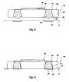
- a portion of an interposer 20includes a substrate 22 with a recess 30 and adjacent conductive traces 24 .
- Substrate 22may be formed of any suitable material, including FR-4 resin and bismaleinidetrizaine (BT) resin, among others.
- the substrate 22may be formed from a flex material, such as polyimide tape.
- a flex materialsuch as polyimide tape.
- Kapton®available from E.I. Du Pont Nemours and Company.
- a recess 30is located in a second surface 28 of the interposer body or substrate 22 .
- Adjacent conductive traces 24are disposed on the opposite, first surface 26 and are accessible through the recess 30 .
- Conductive traces 24may be in electrical communication with a semiconductor die attached to the interposer 20 .
- Conductive traces 24may be formed from any suitable material, including metallic traces made of copper alloys or other metals, a conductive epoxy, a plastic material containing conductive particles, or a conductive ink.
- a conductive element 32may be disposed in the recess 30 , making an electrical connection with the conductive traces 24 therethrough.
- recess 30is configured such that a major portion of the conductive element 32 resides substantially within the recess 30 .
- conductive element 32may be formed from any number of electrically conductive attachment materials suitable for use in the interconnection of interposer 20 with higher level packaging. Examples of conductive elements 32 include solder balls and columnar structures of conductive and conductor-filled epoxies, among others. All such suitable conductive elements 32 are within the scope of the present invention.
- the solder ballsmay be disposed within the recesses by any suitable method. Examples of such methods include: the direct placement of preformed solder balls into a pattern of recesses 30 on the second surface 28 ; the flooding of the second surface 28 with a plurality of solder balls followed by the removal of those balls protruding more than fixed distance from the second surface 28 and therefore not disposed in a recess 30 ; and the disposition of a solder paste directly within the recesses 30 , followed by reflowing the solder to form spherical elements protruding from the openings of recesses 30 or, if the recesses are sized to constrain formulation of spheres, to form hemispherical protrusions of solder from the mouths of recesses 30 .
- a solder maskmay be applied to the second surface 28 to facilitate solder ball formulation in the latter manner.
- Recess 30may be formed in the substrate 22 by any suitable means, including both additive and subtractive methods.
- Blank 10includes a substrate layer 12 and a conductive layer 14 .
- Recess 32may be formed in the substrate layer by the removal of material.
- substrate layer 12may be cut with a laser, drilled, punched, chemically etched, or treated with an electroforming chemical to a depth sufficient to expose conductive layers.
- These subtractive methodsmay utilize a stencil or patterned resist applied to the substrate layer 12 prior to treatment.
- the substrate 22may be formed from an additive method, with the recess 30 preformed in the substrate material and laminated to a conductive layer thru the use of tape adhesive.
- Conductive traces 24may similarly be formed by any suitable method, including both additive and subtractive methods.
- the conductive layer 14may be etched to form a desired pattern of conductive traces 24 . This may be accomplished by applying a stencil or by patterning a and then removing conductive material through a chemical etch or other means.
- the pattern of conductive traces 24may be formed by depositing the conductive traces 24 on the substrate 22 . Any suitable additive technique can be used, such as by preforming the traces 24 or by etching or stamping and applying them to substrate 22 , by applying a conductive polymer to form devices, by printing with a conductive ink, or otherwise as known in the art.
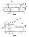
- FIGS. 3 and 4depict a semiconductor assembly 40 made in accordance with the principles of the present invention. It will be appreciated that FIGS. 3 and 4 are not to scale, but are only representative.
- a semiconductor die 54is attached to an interposer 42 . In the depicted embodiment, the semiconductor die 54 is attached in a flip chip fashion, depicted by conductive columns 56 , although it will be appreciated that any method known to those skilled in the art may be used and all such methods are within the scope of the present invention.
- a pattern of conductive traces 40is disposed on the first surface 46 of the interposer 42 . Recesses 50 are located on opposite surface 48 .
- Each of the conductive elements 52 residing substantially within the recesses 50make electrical contact with at least one of the conductive traces 44 , traces 44 being in electrical communication with the semiconductor die 54 through conductive columns 56 .
- the positioning of a number of recesses 50 on the interposer 42may be used to provide a grid array, such as a ball grid array (BGA) or fine ball grid array (FBGA), for attachment and interconnection of the assembly 40 to higher level packaging.
- BGAball grid array
- FBGAfine ball grid array
- Semiconductor assembly 40may be attached to higher level packaging in the form of a carrier substrate S, which may be a printed circuit board (PCB) or any other suitable structure. Assembly 40 is placed on the substrate S, such that the conductive elements 52 are located on and bonded to conductive attachment points, such as the contact pads 58 . It will be appreciated that in addition to contact pads 58 , the attachment points may be formed of any suitable structure, including conductive traces, among others. In embodiments where the conductive elements 52 are solder balls, this may be accomplished by reflowing the solder.
- PCBprinted circuit board
- the positioning of conductive elements 52 substantially within the recesses 50allows the interposer 42 to be mounted closely to the substrate S, reducing the overall height of the assembly 40 .
- the interposer 40 second surface 48may even be disposed directly on the substrate S. This may be accomplished as solder ball conductive elements are reflowed and flow to fill any space remaining around the solder ball within the recess 50 .
- the assembly 40may flex towards the substrate S, further reducing the overall height.
- FIG. 5depicts a side, cross sectional view of a stack of semiconductor assemblies fabricated in accordance with the principles of the present invention. It will be appreciated that FIG. 5, like the other figures in the present application, is not to scale but is instead representational of the principles of the present invention.
- a first semiconductor assembly 70is attached to a substrate S, as discussed above with respect to FIGS. 2 and 3.
- Conductive elements 82substantially residing within recesses 80 are connected to contact pads 88 of the substrate S.
- a semiconductor die 84is disposed on a first surface 76 of the interposer 72 and is in electrical communication with the conductive element 82 through the conductive traces 74 .
- Interposer 72 of assembly 70includes an interconnect structure allowing for connection with another assembly 100 stacked on the first surface 76 .
- the interconnect structureis represented by the interconnect pads 92 .
- Interconnect pads 92function similar to contact pads 88 , allowing another semiconductor assembly to be electrically attached thereto.
- Interconnect pads 92may be connected to the pattern of conductive traces 74 , and to conductive elements 82 therethrough, or may be directly connected to a recess 80 , with a conductive element therein.
- a via or other connective structuremay be used to connect the stacked assembly with either the substrate S or the first assembly 70 .
- a second semiconductor assembly 100is stacked adjacent the first assembly 70 .
- Second assembly 100includes a semiconductor die 114 attached to the first surface 106 of an interposer 102 .
- the semiconductor die 114is in electrical communication with a pattern of conductive traces 104 , located on the first surface 106 , depicted in this embodiment through the wirebond connection 115 .
- Recesses 110are disposed in the second surface 108 and pass through the body of the interposer 102 to allow communication with the conductive traces 104 .
- Each recess 110may allow electrical communication with one or more conductive traces 104 .
- Conductive elements 112are disposed in the recesses 110 and may be used for attachment of the assembly 100 and electrical communication with the semiconductor die 114 .
- second assembly 100includes a solder mask 109 disposed adjacent to the second surface 108 for facilitating the formation of conductive elements 112 .
- the second assemblyfurther includes a die recess 90 accessible on the second surface 108 .
- Die recess 90may be formed in any suitable manner, as discussed above with respect to the interconnection recesses 110 .
- the die recess 90is configured to contain at least a portion of die 84 .
- the dimensions of the die recess 90may vary with different embodiments to accomplish this purpose. If necessary, die recess 90 may extend to or even through the first surface 106 , desirably at a location other than die 114 , or conductive traces 104 .
- Second assembly 100is positioned with second surface 102 adjacent to the first surface 76 of the first assembly 70 . Second assembly 100 is positioned such that conductive elements 112 are aligned with the interconnect pads 92 , and die recess 90 is aligned with die 84 . Conductive elements 112 are then bonded to the interconnect pads 92 , coupling the assemblies into a stacked array, and establishing electrical communication therebetween the assemblies 70 and 100 and the substrate S.
- the first semiconductor assembly, 158includes a semiconductor die 164 attached to the first surface 166 of an interposer 160 .
- Semiconductor die 164is in electrical communication with a pattern of conductive traces 174 disposed on the first surface.
- a recess 170is accessible on the second opposite surface 168 of the interposer.
- a conductive element 172is disposed substantially within the recess. Note that in the depicted embodiment die 164 is encapsulated with an encapsulant material 163 , providing additional protection to the die 164 .
- First assembly 158is attached to a substrate S, with conductive element 172 bonded to contact pad 178 of substrate S, and second surface 168 adjacent to substrate S. It will be appreciated that the embodiment of first assembly 158 , as shown in FIG. 6, may include a plurality of recesses 170 and conductive elements 172 forming an array, such as a ball grid array. All such embodiments are included within the scope of the present invention.
- Second semiconductor assembly 128similarly includes a semiconductor die 134 attached to the first surface 136 of interposer 130 .
- Die 134is in electrical communication with at least one member of a pattern of conductive traces 144 disposed on first surface 136 , depicted here by wirebond 135 .
- Die 134 and the electrical connection to the conductive tracesmay be encapsulated with an encapsulant material 133 .
- An interconnect recess 150is accessible on the opposite second surface 148 and passes into the body of the interposer 130 . At least one member of the conductive traces 144 is accessible through the interconnect recess 150 .
- a conductive element, such as solder ball 152is disposed in the interconnect recess 150 , in an electrically communicative connection with at least one member of the conductive traces 144 .
- second assembly 130may include any number of interconnect recesses 150 and solder balls 152 , forming a grid array on the second surface 148 for connection of the assembly 128 .
- a stack assembly 120is formed by attaching the second surface 148 of second assembly 128 to the first surface 166 of first assembly 158 .
- Recess 150is aligned with an interconnect structure, allowing the assemblies to be attached in electrical communication, through solder ball 152 .
- the interconnect structureis represented as one or more members of conductive traces 174 disposed on first surface 166 of the first assembly 158 .
- the interconnect structuremay be any structure known, or readily ascertainable, to those skilled in the art that may be used establishing electrical communication between first assembly 158 and second assembly 128 . All such structures are within the scope of the present invention.
- solder ball 152is reflowed to attach the interconnect structures of the pattern of conductive traces 174 , any space remaining within recess 150 is filled by solder. This allows second surface 148 to draw closer to the first surface 166 , further reducing the height of the stacked assembly 120 .
- interposer 130is constructed from a flexible material, such as a polyimide tape
- the reduced rigidity of second assembly 128allows further reduction in height.
- a non-rigid embodiment of first assembly 128is able to flex and adjust within the available space, drawing closer to the adjacent assembly 158 .
- FIG. 7is depicted a side, cross sectional view of multiple component stack of semiconductor assemblies fabricated in accordance with the principles of the present invention. It will be appreciated that FIG. 7, like the other figures in the present application, is not to scale but is instead representational of the principles of the present invention.
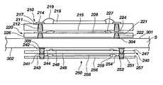
- a first semiconductor assembly 220is attached to a substrate S, which may be a printed circuit board (PCB) or similar structure, as discussed elsewhere herein.
- Conductive elements 222substantially residing within recesses 221 are connected to contact pads 304 of the substrate S, on first surface 301 thereof.
- a semiconductor die 228is disposed on a first surface 227 of the interposer 226 and is in electrical communication with the conductive element 222 through the conductive traces 224 .
- Interposer 226includes an interconnect structure allowing for connection with another assembly 210 stacked on the first surface 227 .
- the interconnect structureis represented by the interconnect pads 224 , as discussed with respect to FIGS. 5 and 6.
- a second semiconductor assembly 210is stacked adjacent the first assembly 220 .
- Second assembly 210includes a semiconductor die 218 attached to the first surface 217 of an interposer 216 .
- the semiconductor die 218is in electrical communication with a pattern of conductive traces 214 , located on the first surface 217 , depicted in this embodiment through the wirebond connection 219 .
- Recesses 211are disposed in the second surface 215 and pass through the body of the interposer 216 to allow communication with the conductive traces 214 .
- Each recess 211may allow electrical communication with one or more conductive traces 214 .
- Conductive elements 212are disposed in the recesses 211 and may be used for attachment of the assembly 210 and electrical communication with the semiconductor die 218 .
- Second assembly 210may include a die recess as in the embodiment of FIG. 5.
- Second assembly 210is positioned with second surface 215 adjacent to the first surface 227 of the first assembly 220 . Second assembly 210 is positioned such that conductive elements 212 are aligned with the interconnect pads 224 . Conductive elements 212 are then bonded to the interconnect pads 224 , coupling the assemblies into a stacked array, and establishing electrical communication therebetween the assemblies 210 and 220 and the substrate S.
- a stack of semiconductor assemblies fabricated in accordance with the principles of the present inventionis located at a second surface 302 of the substrate S.
- a third semiconductor assembly 240is attached to the second surface 302 of substrate S.
- Conductive elements 242substantially residing within recesses 241 are connected to contact pads 305 of the substrate S, on the second surface 302 .
- a semiconductor die 248is disposed on a first surface 247 of the interposer 246 and is in electrical communication with the conductive element 242 through the conductive traces 244 .
- Interposer 246includes an interconnect structure allowing for connection with another assembly 250 stacked on the second surface 249 .
- the interconnect structureis represented by the interconnect pads 243 located on the second surface 249 and similar to those discussed previously herein.
- a fourth semiconductor assembly 250is stacked adjacent the first assembly 240 .
- Fourth assembly 250includes a semiconductor die 258 attached to the first surface 257 of an interposer 256 .
- the semiconductor die 258is in electrical communication with a pattern of conductive traces 254 , located on the first surface 257 , depicted in this embodiment through the wirebond connection 259 .
- Recesses 251are disposed in the first surface 255 and contain a conductive elements 252 protruding slightly therefrom. Conductive elements 252 may be used for attachment of the assembly 250 and electrical communication with the semiconductor die 258 .
- Third assembly 240may include a die recess as in the embodiment of FIG. 5.
- Fourth assembly 250is positioned with first surface 255 adjacent to the second surface 249 of the third assembly 240 . Fourth assembly 250 is positioned such that conductive elements 252 are aligned with the interconnect pads 243 . Conductive elements 252 are then bonded to the interconnect pads 243 , coupling the assemblies into a stacked array, and establishing electrical communication therebetween the assemblies 240 and 250 and the substrate S.
- the stacked assemblies 210 , 220 , 230 and 240are representational only and that as many assemblies as desired may be utilized to forma stacks on a surface of a substrate S. By stacking multiple assemblies on the different surfaces of the substrate S, further reductions of the amount of space consumed by an assembly inside an electronic device may be realized.
- the present inventionincludes a method of forming a stackable semiconductor assembly with recessed interconnections.
- This methodmay be practiced by providing a substrate to form an interposer body having first and second surfaces, then disposing electrically conductive traces on the first surface, disposing a stacking electrical interconnection structure on the first surface and forming a connection recess in the second surface and passing through the interposer body to expose at least one exposed electrically conductive trace disposed on the first surface.
- a semiconductor dieis then provided to the first surface, such that said semiconductor die is in electrical communication with at least one connecting electrically conductive trace disposed on the first surface then an electrically conductive connection material is disposed substantially within the connection recess, such that the electrically conductive material is in electrically conductive contact with the at least one exposed one electrically conductive trace.
- the diemay be attached in conventional or flip chip fashion.
- the act of disposing the electrically conductive compound in the connection recesscould include disposing the electrically conductive compound in electrically conductive contact with the at least one connecting electrically conductive trace.
- the electrically conductive compound connectionmay be a solder paste disposed in the recesses and reflowed to form solder balls.
- the substratemay be a polyimide flex tape, or other material.
- the electrically conductive tracescould be formed by etching a metallic layer disposed on the first surface or by disposing traces directly upon the first surface. An electrically conductive trace may serve as the interconnect structure, or a separate connection pad may be used.
- a die recessmay be formed in the second surface, if desired. It will be appreciated that these options are illustrative only and that other useful options known or readily ascertainable to those skilled in the art may be used.
- the present inventionincludes a method of forming a semiconductor assembly.
- This methodmay be practiced by providing a nonrigid substrate to form an interposer body having first and second surfaces, disposing electrically conductive traces on the first surface and forming a connection recess in the second surface and passing through the interposer body to expose at least one exposed electrically conductive trace disposed on the first surface.
- a semiconductor dieis then provided and attached to the first surface in electrical communication with at least one connecting electrically conductive trace.
- an electrically conductive connection compoundis disposed substantially within the connection recess in electrically conductive contact with the at least one exposed one electrically conductive trace.
- the diemay be attached in conventional or flip chip fashion.
- the act of disposing the electrically conductive compound in the connection recesscould include disposing the electrically conductive compound in electrically conductive contact with the at least one connecting electrically conductive trace.
- the electrically conductive compound connectionmay be a solder paste disposed in the recesses and reflowed to form solder balls, this process may be aided with the application of a solder mask to the second surface. Alternatively, the second surface may be flooded with solder balls, followed by the removal of those that protrude above a certain distance.
- the substratemay be a polyimide flex tape, or other material.
- the electrically conductive tracesmay be formed by etching a metallic layer disposed on the first surface or by disposing traces directly upon the first surface.
- An electrically conductive tracemay serve as the interconnect structure, or a separate connection pad may be used.
- a die recessmay be formed in the second surface, if desired. It will be appreciated that these options are illustrative only and that other useful options known or readily ascertainable to those skilled in the art may be used.
- a first semiconductor assemblyis assembled by taking a first substrate to form a first interposer body having first and second surfaces, disposing first electrically conductive traces on the first surface, forming at least a first connection recess in the second surface and passing through the first interposer body to expose at least one exposed first electrically conductive trace disposed on the first surface, providing a first semiconductor die, attaching the first semiconductor die to the first surface in electrical communication with at least one connecting first electrically conductive trace disposed on the first surface, disposing an electrically conductive connection compound substantially within the at least first connection recess and in electrically conductive contact with the at least one exposed first electrically conductive trace.
- a second semiconductor assemblyis assembled by taking a second substrate to form a second interposer body having third and fourth surfaces, disposing second electrically conductive traces on the third surface, disposing at least a first stacking electrical interconnection structure on the third surface, forming at least a second connection recess in the fourth surface and passing through the second interposer body to expose at least one exposed second electrically conductive trace disposed on the third surface, providing a second semiconductor die, attaching the second semiconductor die to the third surface in electrical communication with at least one connecting second electrically conductive trace disposed on the second surface, and disposing an electrically conductive connection compound substantially within the at least second connection recess and in electrically conductive contact with the at least one exposed one second electrically conductive trace.
- the second surface of the first semiconductor assemblyis attached to the third surface of the second semiconductor assembly, such that the at least first recess is aligned with the stacking electrical interconnection structure, and the electrically conductive connection compound disposed within the at least first recess makes electrically conductive contact to the at least first stacking electrical interconnection structure.
Landscapes
- Engineering & Computer Science (AREA)
- Microelectronics & Electronic Packaging (AREA)
- Power Engineering (AREA)
- Physics & Mathematics (AREA)
- Condensed Matter Physics & Semiconductors (AREA)
- General Physics & Mathematics (AREA)
- Computer Hardware Design (AREA)
- Manufacturing & Machinery (AREA)
- Ceramic Engineering (AREA)
- Wire Bonding (AREA)
- Electric Connection Of Electric Components To Printed Circuits (AREA)
Abstract
Description
- This application is related to U.S. patent application Ser. No. 09/944,465 filed Aug. 30, 2001 and entitled MICROELECTRONIC DEVICES AND METHODS OF MANUFACTURE, and to the following U.S. patent applications filed on even date herewith: Ser. No. (Attorney Docket No. 4812US), entitled INTERPOSER CONFIGURED TO REDUCE THE PROFILES OF SEMICONDUCTOR DEVICE ASSEMBLIES AND PACKAGES INCLUDING THE SAME AND METHODS; Ser. No. (Attorney Docket No. 4877US), entitled METHOD AND APPARATUS FOR FLIP-CHIP PACKAGING PROVIDING TESTING CAPABILITY; Ser. No. (Attorney Docket No. 4879US), entitled FLIP CHIP PACKAGING USING RECESSED INTERPOSER TERMINALS; Ser. No. (Attorney Docket No. 4973US), entitled METHOD AND APPARATUS FOR DIELECTRIC FILLING OF FLIP CHIP ON INTERPOSER ASSEMBLY; and Ser. No. (Attorney Docket No. 4974US), entitled METHODS FOR ASSEMBLY AND PACKAGING OF FLIP CHIP CONFIGURED DICE WITH INTERPOSER.[0001]
- 1. Field of the Invention[0002]
- The present invention relates to ball grid array semiconductor packages and methods of attaching, and interconnecting the same. In particular, the present invention relates to interposers for mounting a semiconductor die to a substrate with which the semiconductor die is in electrical communication The semiconductor die may be encapsulated upon the interposer to form a complete semiconductor die package. The interposer may be constructed in order to allow a number of similar semiconductor die packages to be electrically connected to a single substrate in a stack.[0003]
- 2. State of the Art[0004]
- Ball grid array (“BGA”) packages are well known in the art. BGA packages typically comprise a substrate, such as a printed circuit board, with a semiconductor die mounted on top of the substrate. The semiconductor die has a multitude of bond pads electrically connected to a series of metal traces on the top side of the printed circuit board. This series of metal traces is connected to a second series of metal traces located on the underside of the printed circuit board by a series of vias. The second series of metal traces each terminate with a contact pad where a conductive element is attached. The conductive elements are typically solder balls or conductive filled epoxy. The conductive elements are arranged in an array pattern and the semiconductor die along with its electrical connections are encapsulated with a molding compound.[0005]
- As die and grid array densities increase, the desire in packaging semiconductor dies has been to reduce the overall size of the package, allowing the mounted packages to take up less “real estate” or area within a device. A BGA package mounted in a flip chip fashion conserves real estate laterally by eliminating the connection structures (wirebond, TAB, etc) around the package. Conserving real estate vertically presents different challenges. One way this has been accomplished is by reducing the overall height or profile of BGA packages. Another way is by using molded packages with leadframes that can be stacked atop one another.[0006]
- Stacking BGA packages allows additional lateral real estate to be conserved in exchange for vertical space. The height of a BGA package, including the substrate, semiconductor die, wirebonds, encapsulant and conductive elements, limits the effectiveness of this method. One example of an attempt to reduce the height of BGA packages in a stack is disclosed in U.S. Pat. No. 6,072,233 issued to Corisis et al Jun. 6, 2000. The disclosed packages consist of a semiconductor die mounted face down on a thin substrate. The die is electrically connected to the substrate by centrally located wirebonds, which are encapsulated on the base of the substrate. Solder balls which have a height greater than the combined heights of the mounted semiconductor die and the wirebond encapsulant are spaced along the perimeter of the substrate. By moving the encapsulant to the lower surface of the package and using a thin substrate a fine ball grid array (FBGA) can be used, reducing the overall height of a package. The ability to reduce the height of the package is still limited by the placement and size restrictions on the solder balls, which must have a diameter greater than the combined heights of the semiconductor dies and wirebond encapsulant. The substrate must be rigid to hold the individual packages apart. The solder balls are exposed at the side of the stack, increasing the chances of breakage or contamination.[0007]
- Therefore, it would be advantageous to develop an apparatus and method that allows for the height of stacked packages to be reduced in comparison to conventional packages. It would further be advantageous for such an apparatus and method to provide for at least enclosing the conductive elements, providing enhanced support as well as protection from breakage and contamination. It would be an additional advantage for certain embodiments of such an apparatus and method to employ at least somewhat flexible substrates, allowing use in increased applications.[0008]
- The present invention includes apparatus and methods for preparing semiconductor device packages, or assemblies. An interposer may be constructed from a flexible material, such as a polyimide tape. A pattern of conductive traces is disposed on a first surface of the interposer in electrical communication with a semiconductor die attached to that first surface. Interconnect recesses accessible are opposite, second surface each allow contact with at least one conductive trace. A conductive element, such as a solder ball, disposed substantially within the interconnect recess is used to mechanically and electrically connect the assembly to a carrier substrate or to another, similar assembly. By substantially receiving the conductive element within the interconnect recess, the height of the completed assembly is reduced.[0009]
- A number of assemblies may be stacked to form stacked semiconductor arrays. Interconnect structures, such as connection pads, or enlarged traces upon the first surface may allow for interaction between stacked assemblies. Assemblies may be stacked stepwise, or directly aligned.[0010]
- FIG. 1 is a side view of a substrate useful in assembling some embodiments of devices made in accordance with the principles of the present invention;[0011]
- FIG. 2 is a sectional side view of a portion of one embodiment of an interposer made in accordance with the principles of the present invention;[0012]
- FIG. 3 is a sectional side view of one embodiment of a semiconductor package made in accordance with the principles of the present invention, shown prior to mounting;[0013]
- FIG. 4 is a sectional side view of the embodiment of FIG. 3, as attached to a substrate;[0014]
- FIG. 5 is a sectional side view of one possible stacked assembly of two alternative embodiments of semiconductor packages made in accordance with the principles of the present invention;[0015]
- FIG. 6 is a sectional side view of a portion of another stacked assembly of a fourth alternative embodiment of semiconductor packages made in accordance with the principles of the present invention; and[0016]
- FIG. 7 is a side, cross sectional view of one embodiment of a multiple component stack of semiconductor assemblies fabricated in accordance with the principles of the present invention.[0017]
- Reference will now be made to FIGS. 1 and 2. A portion of an[0018]
interposer 20 includes asubstrate 22 with arecess 30 and adjacent conductive traces24.Substrate 22 may be formed of any suitable material, including FR-4 resin and bismaleinidetrizaine (BT) resin, among others. In embodiments where it is desired thatinterposer 20 have flexibility, thesubstrate 22 may be formed from a flex material, such as polyimide tape. One such suitable tape is Kapton®, available from E.I. Du Pont Nemours and Company. - A[0019]
recess 30 is located in asecond surface 28 of the interposer body orsubstrate 22. Adjacentconductive traces 24 are disposed on the opposite,first surface 26 and are accessible through therecess 30. Conductive traces24 may be in electrical communication with a semiconductor die attached to theinterposer 20. Conductive traces24 may be formed from any suitable material, including metallic traces made of copper alloys or other metals, a conductive epoxy, a plastic material containing conductive particles, or a conductive ink. - A[0020]
conductive element 32 may be disposed in therecess 30, making an electrical connection with theconductive traces 24 therethrough. Desirably,recess 30 is configured such that a major portion of theconductive element 32 resides substantially within therecess 30. It will be appreciated thatconductive element 32 may be formed from any number of electrically conductive attachment materials suitable for use in the interconnection ofinterposer 20 with higher level packaging. Examples ofconductive elements 32 include solder balls and columnar structures of conductive and conductor-filled epoxies, among others. All such suitableconductive elements 32 are within the scope of the present invention. - Where the[0021]
conductive elements 32 comprise solder balls, the solder balls may be disposed within the recesses by any suitable method. Examples of such methods include: the direct placement of preformed solder balls into a pattern ofrecesses 30 on thesecond surface 28; the flooding of thesecond surface 28 with a plurality of solder balls followed by the removal of those balls protruding more than fixed distance from thesecond surface 28 and therefore not disposed in arecess 30; and the disposition of a solder paste directly within therecesses 30, followed by reflowing the solder to form spherical elements protruding from the openings ofrecesses 30 or, if the recesses are sized to constrain formulation of spheres, to form hemispherical protrusions of solder from the mouths ofrecesses 30. A solder mask may be applied to thesecond surface 28 to facilitate solder ball formulation in the latter manner. - [0022]
Recess 30 may be formed in thesubstrate 22 by any suitable means, including both additive and subtractive methods. In FIG. 1 is depicted a substrate blank10 that may be used for forming some embodiments ofinterposers 30 in accordance with the present invention.Blank 10 includes asubstrate layer 12 and aconductive layer 14.Recess 32 may be formed in the substrate layer by the removal of material. For example,substrate layer 12 may be cut with a laser, drilled, punched, chemically etched, or treated with an electroforming chemical to a depth sufficient to expose conductive layers. These subtractive methods may utilize a stencil or patterned resist applied to thesubstrate layer 12 prior to treatment. In alternative embodiments, thesubstrate 22 may be formed from an additive method, with therecess 30 preformed in the substrate material and laminated to a conductive layer thru the use of tape adhesive. - Conductive traces[0023]24 may similarly be formed by any suitable method, including both additive and subtractive methods. In FIG. 1, the
conductive layer 14 may be etched to form a desired pattern of conductive traces24. This may be accomplished by applying a stencil or by patterning a and then removing conductive material through a chemical etch or other means. In alternative embodiments, the pattern ofconductive traces 24 may be formed by depositing the conductive traces24 on thesubstrate 22. Any suitable additive technique can be used, such as by preforming thetraces 24 or by etching or stamping and applying them tosubstrate 22, by applying a conductive polymer to form devices, by printing with a conductive ink, or otherwise as known in the art. - FIGS. 3 and 4 depict a[0024]
semiconductor assembly 40 made in accordance with the principles of the present invention. It will be appreciated that FIGS. 3 and 4 are not to scale, but are only representative. A semiconductor die54 is attached to aninterposer 42. In the depicted embodiment, the semiconductor die54 is attached in a flip chip fashion, depicted byconductive columns 56, although it will be appreciated that any method known to those skilled in the art may be used and all such methods are within the scope of the present invention. A pattern ofconductive traces 40 is disposed on thefirst surface 46 of theinterposer 42.Recesses 50 are located onopposite surface 48. Each of theconductive elements 52 residing substantially within therecesses 50 make electrical contact with at least one of the conductive traces44, traces44 being in electrical communication with the semiconductor die54 throughconductive columns 56. The positioning of a number ofrecesses 50 on theinterposer 42 may be used to provide a grid array, such as a ball grid array (BGA) or fine ball grid array (FBGA), for attachment and interconnection of theassembly 40 to higher level packaging. - [0025]
Semiconductor assembly 40 may be attached to higher level packaging in the form of a carrier substrate S, which may be a printed circuit board (PCB) or any other suitable structure.Assembly 40 is placed on the substrate S, such that theconductive elements 52 are located on and bonded to conductive attachment points, such as thecontact pads 58. It will be appreciated that in addition tocontact pads 58, the attachment points may be formed of any suitable structure, including conductive traces, among others. In embodiments where theconductive elements 52 are solder balls, this may be accomplished by reflowing the solder. - The positioning of[0026]
conductive elements 52 substantially within therecesses 50 allows theinterposer 42 to be mounted closely to the substrate S, reducing the overall height of theassembly 40. In certain embodiments, theinterposer 40second surface 48 may even be disposed directly on the substrate S. This may be accomplished as solder ball conductive elements are reflowed and flow to fill any space remaining around the solder ball within therecess 50. With embodiments where theinterposer 42 has reduced rigidity, as when formed from a polymide tape, theassembly 40 may flex towards the substrate S, further reducing the overall height. - FIG. 5 depicts a side, cross sectional view of a stack of semiconductor assemblies fabricated in accordance with the principles of the present invention. It will be appreciated that FIG. 5, like the other figures in the present application, is not to scale but is instead representational of the principles of the present invention. A[0027]
first semiconductor assembly 70 is attached to a substrate S, as discussed above with respect to FIGS. 2 and 3.Conductive elements 82, substantially residing withinrecesses 80 are connected to contactpads 88 of the substrate S. A semiconductor die84 is disposed on afirst surface 76 of the interposer72 and is in electrical communication with theconductive element 82 through the conductive traces74. Interposer72 ofassembly 70 includes an interconnect structure allowing for connection with anotherassembly 100 stacked on thefirst surface 76. In the depicted embodiment, the interconnect structure is represented by theinterconnect pads 92.Interconnect pads 92 function similar to contactpads 88, allowing another semiconductor assembly to be electrically attached thereto.Interconnect pads 92 may be connected to the pattern ofconductive traces 74, and toconductive elements 82 therethrough, or may be directly connected to arecess 80, with a conductive element therein. Alternatively, a via or other connective structure may be used to connect the stacked assembly with either the substrate S or thefirst assembly 70. - A[0028]
second semiconductor assembly 100 is stacked adjacent thefirst assembly 70.Second assembly 100 includes asemiconductor die 114 attached to thefirst surface 106 of aninterposer 102. The semiconductor die114 is in electrical communication with a pattern ofconductive traces 104, located on thefirst surface 106, depicted in this embodiment through thewirebond connection 115.Recesses 110 are disposed in thesecond surface 108 and pass through the body of theinterposer 102 to allow communication with the conductive traces104. Eachrecess 110 may allow electrical communication with one or more conductive traces104.Conductive elements 112 are disposed in therecesses 110 and may be used for attachment of theassembly 100 and electrical communication with the semiconductor die114. Note thatsecond assembly 100 includes asolder mask 109 disposed adjacent to thesecond surface 108 for facilitating the formation ofconductive elements 112. - The second assembly further includes a[0029]
die recess 90 accessible on thesecond surface 108. Dierecess 90 may be formed in any suitable manner, as discussed above with respect to the interconnection recesses110. Thedie recess 90 is configured to contain at least a portion ofdie 84. The dimensions of thedie recess 90 may vary with different embodiments to accomplish this purpose. If necessary, dierecess 90 may extend to or even through thefirst surface 106, desirably at a location other than die114, or conductive traces104. - [0030]
Second assembly 100 is positioned withsecond surface 102 adjacent to thefirst surface 76 of thefirst assembly 70.Second assembly 100 is positioned such thatconductive elements 112 are aligned with theinterconnect pads 92, and dierecess 90 is aligned withdie 84.Conductive elements 112 are then bonded to theinterconnect pads 92, coupling the assemblies into a stacked array, and establishing electrical communication therebetween theassemblies - Turning to FIG. 6, there is depicted a portion of a[0031]
stack 120 ofsemiconductor assemblies semiconductor die 164 attached to thefirst surface 166 of aninterposer 160. Semiconductor die164 is in electrical communication with a pattern ofconductive traces 174 disposed on the first surface. Arecess 170 is accessible on the secondopposite surface 168 of the interposer. Aconductive element 172 is disposed substantially within the recess. Note that in the depicted embodiment die164 is encapsulated with anencapsulant material 163, providing additional protection to thedie 164.First assembly 158 is attached to a substrate S, withconductive element 172 bonded to contactpad 178 of substrate S, andsecond surface 168 adjacent to substrate S. It will be appreciated that the embodiment offirst assembly 158, as shown in FIG. 6, may include a plurality ofrecesses 170 andconductive elements 172 forming an array, such as a ball grid array. All such embodiments are included within the scope of the present invention. - [0032]
Second semiconductor assembly 128 similarly includes asemiconductor die 134 attached to thefirst surface 136 ofinterposer 130.Die 134 is in electrical communication with at least one member of a pattern ofconductive traces 144 disposed onfirst surface 136, depicted here bywirebond 135.Die 134 and the electrical connection to the conductive traces may be encapsulated with anencapsulant material 133. Aninterconnect recess 150 is accessible on the oppositesecond surface 148 and passes into the body of theinterposer 130. At least one member of the conductive traces144 is accessible through theinterconnect recess 150. A conductive element, such assolder ball 152 is disposed in theinterconnect recess 150, in an electrically communicative connection with at least one member of the conductive traces144. It will be appreciated thatsecond assembly 130 may include any number of interconnect recesses150 andsolder balls 152, forming a grid array on thesecond surface 148 for connection of theassembly 128. - A[0033]
stack assembly 120 is formed by attaching thesecond surface 148 ofsecond assembly 128 to thefirst surface 166 offirst assembly 158.Recess 150 is aligned with an interconnect structure, allowing the assemblies to be attached in electrical communication, throughsolder ball 152. In the embodiment depicted in FIG. 6, the interconnect structure is represented as one or more members ofconductive traces 174 disposed onfirst surface 166 of thefirst assembly 158. As discussed above, the interconnect structure may be any structure known, or readily ascertainable, to those skilled in the art that may be used establishing electrical communication betweenfirst assembly 158 andsecond assembly 128. All such structures are within the scope of the present invention. - As[0034]
solder ball 152 is reflowed to attach the interconnect structures of the pattern ofconductive traces 174, any space remaining withinrecess 150 is filled by solder. This allowssecond surface 148 to draw closer to thefirst surface 166, further reducing the height of the stackedassembly 120. In embodiments whereinterposer 130 is constructed from a flexible material, such as a polyimide tape, the reduced rigidity ofsecond assembly 128 allows further reduction in height. A non-rigid embodiment offirst assembly 128 is able to flex and adjust within the available space, drawing closer to theadjacent assembly 158. Through these attributes, some embodiments of the present invention may be used to create stacks of semiconductor assemblies with a reduction in the overall height of the stacked assemblies, conserving real estate in a device in both lateral and vertical directions. - Turning to FIG. 7 is depicted a side, cross sectional view of multiple component stack of semiconductor assemblies fabricated in accordance with the principles of the present invention. It will be appreciated that FIG. 7, like the other figures in the present application, is not to scale but is instead representational of the principles of the present invention. Similar to FIG. 5, a[0035]
first semiconductor assembly 220 is attached to a substrate S, which may be a printed circuit board (PCB) or similar structure, as discussed elsewhere herein. Conductive elements222, substantially residing withinrecesses 221 are connected to contactpads 304 of the substrate S, on first surface301 thereof. A semiconductor die228 is disposed on afirst surface 227 of theinterposer 226 and is in electrical communication with the conductive element222 through the conductive traces224.Interposer 226 includes an interconnect structure allowing for connection with anotherassembly 210 stacked on thefirst surface 227. In the depicted embodiment, the interconnect structure is represented by theinterconnect pads 224, as discussed with respect to FIGS. 5 and 6. - A[0036]
second semiconductor assembly 210 is stacked adjacent thefirst assembly 220.Second assembly 210 includes asemiconductor die 218 attached to thefirst surface 217 of an interposer216. The semiconductor die218 is in electrical communication with a pattern ofconductive traces 214, located on thefirst surface 217, depicted in this embodiment through thewirebond connection 219.Recesses 211 are disposed in thesecond surface 215 and pass through the body of the interposer216 to allow communication with the conductive traces214. Eachrecess 211 may allow electrical communication with one or more conductive traces214.Conductive elements 212 are disposed in therecesses 211 and may be used for attachment of theassembly 210 and electrical communication with the semiconductor die218.Second assembly 210 may include a die recess as in the embodiment of FIG. 5. - [0037]
Second assembly 210 is positioned withsecond surface 215 adjacent to thefirst surface 227 of thefirst assembly 220.Second assembly 210 is positioned such thatconductive elements 212 are aligned with theinterconnect pads 224.Conductive elements 212 are then bonded to theinterconnect pads 224, coupling the assemblies into a stacked array, and establishing electrical communication therebetween theassemblies - Similarly, a stack of semiconductor assemblies fabricated in accordance with the principles of the present invention is located at a[0038]
second surface 302 of the substrate S. Athird semiconductor assembly 240 is attached to thesecond surface 302 of substrateS. Conductive elements 242, substantially residing withinrecesses 241 are connected to contactpads 305 of the substrate S, on thesecond surface 302. A semiconductor die248 is disposed on afirst surface 247 of the interposer246 and is in electrical communication with theconductive element 242 through the conductive traces244. Interposer246 includes an interconnect structure allowing for connection with anotherassembly 250 stacked on thesecond surface 249. In the depicted embodiment, the interconnect structure is represented by theinterconnect pads 243 located on thesecond surface 249 and similar to those discussed previously herein. - A[0039]
fourth semiconductor assembly 250 is stacked adjacent thefirst assembly 240.Fourth assembly 250 includes asemiconductor die 258 attached to thefirst surface 257 of aninterposer 256. The semiconductor die258 is in electrical communication with a pattern ofconductive traces 254, located on thefirst surface 257, depicted in this embodiment through thewirebond connection 259.Recesses 251 are disposed in the first surface255 and contain aconductive elements 252 protruding slightly therefrom.Conductive elements 252 may be used for attachment of theassembly 250 and electrical communication with the semiconductor die258.Third assembly 240 may include a die recess as in the embodiment of FIG. 5. - [0040]
Fourth assembly 250 is positioned with first surface255 adjacent to thesecond surface 249 of thethird assembly 240.Fourth assembly 250 is positioned such thatconductive elements 252 are aligned with theinterconnect pads 243.Conductive elements 252 are then bonded to theinterconnect pads 243, coupling the assemblies into a stacked array, and establishing electrical communication therebetween theassemblies - It will be appreciated that the stacked[0041]
assemblies - In accordance with the description provided, the present invention includes a method of forming a stackable semiconductor assembly with recessed interconnections. This method may be practiced by providing a substrate to form an interposer body having first and second surfaces, then disposing electrically conductive traces on the first surface, disposing a stacking electrical interconnection structure on the first surface and forming a connection recess in the second surface and passing through the interposer body to expose at least one exposed electrically conductive trace disposed on the first surface. A semiconductor die is then provided to the first surface, such that said semiconductor die is in electrical communication with at least one connecting electrically conductive trace disposed on the first surface then an electrically conductive connection material is disposed substantially within the connection recess, such that the electrically conductive material is in electrically conductive contact with the at least one exposed one electrically conductive trace.[0042]
- When the method is practiced, a number of options may be utilized to optimize the procedure. For example, the die may be attached in conventional or flip chip fashion. The act of disposing the electrically conductive compound in the connection recess could include disposing the electrically conductive compound in electrically conductive contact with the at least one connecting electrically conductive trace. The electrically conductive compound connection may be a solder paste disposed in the recesses and reflowed to form solder balls. The substrate may be a polyimide flex tape, or other material. The electrically conductive traces could be formed by etching a metallic layer disposed on the first surface or by disposing traces directly upon the first surface. An electrically conductive trace may serve as the interconnect structure, or a separate connection pad may be used. Further, a die recess may be formed in the second surface, if desired. It will be appreciated that these options are illustrative only and that other useful options known or readily ascertainable to those skilled in the art may be used.[0043]
- Further, it will be appreciated that the present invention includes a method of forming a semiconductor assembly. This method may be practiced by providing a nonrigid substrate to form an interposer body having first and second surfaces, disposing electrically conductive traces on the first surface and forming a connection recess in the second surface and passing through the interposer body to expose at least one exposed electrically conductive trace disposed on the first surface. A semiconductor die is then provided and attached to the first surface in electrical communication with at least one connecting electrically conductive trace. Next, an electrically conductive connection compound is disposed substantially within the connection recess in electrically conductive contact with the at least one exposed one electrically conductive trace.[0044]
- As above, when this method is practiced, a number of options can be utilized to optimize the procedure. For example, the die may be attached in conventional or flip chip fashion. The act of disposing the electrically conductive compound in the connection recess could include disposing the electrically conductive compound in electrically conductive contact with the at least one connecting electrically conductive trace. The electrically conductive compound connection may be a solder paste disposed in the recesses and reflowed to form solder balls, this process may be aided with the application of a solder mask to the second surface. Alternatively, the second surface may be flooded with solder balls, followed by the removal of those that protrude above a certain distance. The substrate may be a polyimide flex tape, or other material. The electrically conductive traces may be formed by etching a metallic layer disposed on the first surface or by disposing traces directly upon the first surface. An electrically conductive trace may serve as the interconnect structure, or a separate connection pad may be used. Further, a die recess may be formed in the second surface, if desired. It will be appreciated that these options are illustrative only and that other useful options known or readily ascertainable to those skilled in the art may be used.[0045]
- It will be appreciated that the present invention also includes a method of forming a stack of semiconductor assemblies. A first semiconductor assembly is assembled by taking a first substrate to form a first interposer body having first and second surfaces, disposing first electrically conductive traces on the first surface, forming at least a first connection recess in the second surface and passing through the first interposer body to expose at least one exposed first electrically conductive trace disposed on the first surface, providing a first semiconductor die, attaching the first semiconductor die to the first surface in electrical communication with at least one connecting first electrically conductive trace disposed on the first surface, disposing an electrically conductive connection compound substantially within the at least first connection recess and in electrically conductive contact with the at least one exposed first electrically conductive trace. A second semiconductor assembly is assembled by taking a second substrate to form a second interposer body having third and fourth surfaces, disposing second electrically conductive traces on the third surface, disposing at least a first stacking electrical interconnection structure on the third surface, forming at least a second connection recess in the fourth surface and passing through the second interposer body to expose at least one exposed second electrically conductive trace disposed on the third surface, providing a second semiconductor die, attaching the second semiconductor die to the third surface in electrical communication with at least one connecting second electrically conductive trace disposed on the second surface, and disposing an electrically conductive connection compound substantially within the at least second connection recess and in electrically conductive contact with the at least one exposed one second electrically conductive trace. The second surface of the first semiconductor assembly is attached to the third surface of the second semiconductor assembly, such that the at least first recess is aligned with the stacking electrical interconnection structure, and the electrically conductive connection compound disposed within the at least first recess makes electrically conductive contact to the at least first stacking electrical interconnection structure.[0046]
- It will be apparent that details of the apparatus and methods herein described can be varied considerably without departing from the concept and scope of the invention. The claims alone define the scope of the invention as conceived and as described herein.[0047]
Claims (105)
Priority Applications (2)
| Application Number | Priority Date | Filing Date | Title |
|---|---|---|---|
| US10/933,060US7230330B2 (en) | 2002-03-04 | 2004-09-01 | Semiconductor die packages with recessed interconnecting structures |
| US11/760,458US7569473B2 (en) | 2002-03-04 | 2007-06-08 | Methods of forming semiconductor assemblies |
Applications Claiming Priority (2)
| Application Number | Priority Date | Filing Date | Title |
|---|---|---|---|
| SG200201290ASG115456A1 (en) | 2002-03-04 | 2002-03-04 | Semiconductor die packages with recessed interconnecting structures and methods for assembling the same |
| SG200201290-4 | 2002-03-04 |
Related Child Applications (1)
| Application Number | Title | Priority Date | Filing Date |
|---|---|---|---|
| US10/933,060DivisionUS7230330B2 (en) | 2002-03-04 | 2004-09-01 | Semiconductor die packages with recessed interconnecting structures |
Publications (2)
| Publication Number | Publication Date |
|---|---|
| US20030164540A1true US20030164540A1 (en) | 2003-09-04 |
| US7112520B2 US7112520B2 (en) | 2006-09-26 |
Family
ID=27800899
Family Applications (3)
| Application Number | Title | Priority Date | Filing Date |
|---|---|---|---|
| US10/150,516Expired - Fee RelatedUS7112520B2 (en) | 2002-03-04 | 2002-05-17 | Semiconductor die packages with recessed interconnecting structures and methods for assembling the same |
| US10/933,060Expired - Fee RelatedUS7230330B2 (en) | 2002-03-04 | 2004-09-01 | Semiconductor die packages with recessed interconnecting structures |
| US11/760,458Expired - LifetimeUS7569473B2 (en) | 2002-03-04 | 2007-06-08 | Methods of forming semiconductor assemblies |
Family Applications After (2)
| Application Number | Title | Priority Date | Filing Date |
|---|---|---|---|
| US10/933,060Expired - Fee RelatedUS7230330B2 (en) | 2002-03-04 | 2004-09-01 | Semiconductor die packages with recessed interconnecting structures |
| US11/760,458Expired - LifetimeUS7569473B2 (en) | 2002-03-04 | 2007-06-08 | Methods of forming semiconductor assemblies |
Country Status (2)
| Country | Link |
|---|---|
| US (3) | US7112520B2 (en) |
| SG (1) | SG115456A1 (en) |
Cited By (72)
| Publication number | Priority date | Publication date | Assignee | Title |
|---|---|---|---|---|
| US20040095736A1 (en)* | 2002-11-18 | 2004-05-20 | Samsung Electronics Co., Ltd. | Multi-chip package having increased reliabilty |
| US6756251B2 (en) | 2001-08-21 | 2004-06-29 | Micron Technology, Inc. | Method of manufacturing microelectronic devices, including methods of underfilling microelectronic components through an underfill aperture |
| US20040212965A1 (en)* | 2003-03-17 | 2004-10-28 | Toshiaki Ishii | Electronic circuit apparatus and method of manufacturing the same |
| US20040262733A1 (en)* | 2003-06-30 | 2004-12-30 | Takashi Kumamoto | Scalable microelectronic package using conductive risers |
| US20050173805A1 (en)* | 2003-12-30 | 2005-08-11 | Tessera, Inc. | Micro pin grid array with pin motion isolation |
| US20050181655A1 (en)* | 2003-12-30 | 2005-08-18 | Tessera, Inc. | Micro pin grid array with wiping action |
| US20050181544A1 (en)* | 2003-12-30 | 2005-08-18 | Tessera, Inc. | Microelectronic packages and methods therefor |
| US20050194672A1 (en)* | 2003-11-04 | 2005-09-08 | Tessera, Inc. | Stacked packages and systems incorporating the same |
| US20050284658A1 (en)* | 2003-10-06 | 2005-12-29 | Tessera, Inc. | Components with posts and pads |
| US20060249857A1 (en)* | 2005-03-16 | 2006-11-09 | Tessera, Inc. | Microelectronic packages and methods therefor |
| US20070148819A1 (en)* | 2005-12-23 | 2007-06-28 | Tessera, Inc. | Microelectronic assemblies having very fine pitch stacking |
| US20070148822A1 (en)* | 2005-12-23 | 2007-06-28 | Tessera, Inc. | Microelectronic packages and methods therefor |
| US20080003402A1 (en)* | 2003-10-06 | 2008-01-03 | Tessera, Inc. | Fine pitch microcontacts and method for forming thereof |
| US20080122113A1 (en)* | 2006-08-17 | 2008-05-29 | Corisis David J | Semiconductor device assemblies and systems including at least one conductive pathway extending around a side of at least one semiconductor device and methods for forming the same |
| US7462936B2 (en) | 2003-10-06 | 2008-12-09 | Tessera, Inc. | Formation of circuitry with modification of feature height |
| US20100044860A1 (en)* | 2008-08-21 | 2010-02-25 | Tessera Interconnect Materials, Inc. | Microelectronic substrate or element having conductive pads and metal posts joined thereto using bond layer |
| US20110220610A1 (en)* | 2006-10-03 | 2011-09-15 | Tredwell Timothy J | Flexible substrate with electronic devices and traces |
| US20120302054A1 (en)* | 2004-08-19 | 2012-11-29 | Micron Technology, Inc. | Conductive structures for microfeature devices and methods for fabricating microfeature devices |
| US8330272B2 (en) | 2010-07-08 | 2012-12-11 | Tessera, Inc. | Microelectronic packages with dual or multiple-etched flip-chip connectors |
| US8404520B1 (en) | 2011-10-17 | 2013-03-26 | Invensas Corporation | Package-on-package assembly with wire bond vias |
| US8482111B2 (en) | 2010-07-19 | 2013-07-09 | Tessera, Inc. | Stackable molded microelectronic packages |
| US8525314B2 (en) | 2004-11-03 | 2013-09-03 | Tessera, Inc. | Stacked packaging improvements |
| US8580607B2 (en) | 2010-07-27 | 2013-11-12 | Tessera, Inc. | Microelectronic packages with nanoparticle joining |
| US8623706B2 (en) | 2010-11-15 | 2014-01-07 | Tessera, Inc. | Microelectronic package with terminals on dielectric mass |
| US8835228B2 (en) | 2012-05-22 | 2014-09-16 | Invensas Corporation | Substrate-less stackable package with wire-bond interconnect |
| US8853558B2 (en) | 2010-12-10 | 2014-10-07 | Tessera, Inc. | Interconnect structure |
| US8872318B2 (en) | 2011-08-24 | 2014-10-28 | Tessera, Inc. | Through interposer wire bond using low CTE interposer with coarse slot apertures |
| US8878353B2 (en) | 2012-12-20 | 2014-11-04 | Invensas Corporation | Structure for microelectronic packaging with bond elements to encapsulation surface |
| US8884448B2 (en) | 2007-09-28 | 2014-11-11 | Tessera, Inc. | Flip chip interconnection with double post |
| US8883563B1 (en) | 2013-07-15 | 2014-11-11 | Invensas Corporation | Fabrication of microelectronic assemblies having stack terminals coupled by connectors extending through encapsulation |
| US8975738B2 (en) | 2012-11-12 | 2015-03-10 | Invensas Corporation | Structure for microelectronic packaging with terminals on dielectric mass |
| US20150084211A1 (en)* | 2012-08-08 | 2015-03-26 | Taiwan Semiconductor Manufacturing Company, Ltd. | Package Assembly and Methods for Forming the Same |
| US9023691B2 (en) | 2013-07-15 | 2015-05-05 | Invensas Corporation | Microelectronic assemblies with stack terminals coupled by connectors extending through encapsulation |
| US9034696B2 (en) | 2013-07-15 | 2015-05-19 | Invensas Corporation | Microelectronic assemblies having reinforcing collars on connectors extending through encapsulation |
| US9082753B2 (en) | 2013-11-12 | 2015-07-14 | Invensas Corporation | Severing bond wire by kinking and twisting |
| US9087815B2 (en) | 2013-11-12 | 2015-07-21 | Invensas Corporation | Off substrate kinking of bond wire |
| US9093435B2 (en) | 2011-05-03 | 2015-07-28 | Tessera, Inc. | Package-on-package assembly with wire bonds to encapsulation surface |
| US9159708B2 (en) | 2010-07-19 | 2015-10-13 | Tessera, Inc. | Stackable molded microelectronic packages with area array unit connectors |
| US9214454B2 (en) | 2014-03-31 | 2015-12-15 | Invensas Corporation | Batch process fabrication of package-on-package microelectronic assemblies |
| US9224717B2 (en) | 2011-05-03 | 2015-12-29 | Tessera, Inc. | Package-on-package assembly with wire bonds to encapsulation surface |
| US20150380340A1 (en)* | 2014-06-27 | 2015-12-31 | Taiwan Semiconductor Manufacturing Company, Ltd. | Methods of Packaging Semiconductor Devices and Packaged Semiconductor Devices |
| US9324681B2 (en) | 2010-12-13 | 2016-04-26 | Tessera, Inc. | Pin attachment |
| US9349706B2 (en) | 2012-02-24 | 2016-05-24 | Invensas Corporation | Method for package-on-package assembly with wire bonds to encapsulation surface |
| US9391008B2 (en) | 2012-07-31 | 2016-07-12 | Invensas Corporation | Reconstituted wafer-level package DRAM |
| US9412714B2 (en) | 2014-05-30 | 2016-08-09 | Invensas Corporation | Wire bond support structure and microelectronic package including wire bonds therefrom |
| US20160276174A1 (en)* | 2015-03-18 | 2016-09-22 | Amkor Technology, Inc. | Semiconductor device and manufacturing method thereof |
| WO2016149441A1 (en)* | 2015-03-18 | 2016-09-22 | Amkor Technology, Inc. | Semiconductor device and manufacturing method thereof |
| US9502390B2 (en) | 2012-08-03 | 2016-11-22 | Invensas Corporation | BVA interposer |
| US20170040248A1 (en)* | 2014-12-05 | 2017-02-09 | Siliconware Precision Industries Co., Ltd. | Electronic package and method of fabricating the same |
| US9583411B2 (en) | 2014-01-17 | 2017-02-28 | Invensas Corporation | Fine pitch BVA using reconstituted wafer with area array accessible for testing |
| US9601454B2 (en) | 2013-02-01 | 2017-03-21 | Invensas Corporation | Method of forming a component having wire bonds and a stiffening layer |
| US9633971B2 (en) | 2015-07-10 | 2017-04-25 | Invensas Corporation | Structures and methods for low temperature bonding using nanoparticles |
| US9646917B2 (en) | 2014-05-29 | 2017-05-09 | Invensas Corporation | Low CTE component with wire bond interconnects |
| US9659848B1 (en) | 2015-11-18 | 2017-05-23 | Invensas Corporation | Stiffened wires for offset BVA |
| US9685365B2 (en) | 2013-08-08 | 2017-06-20 | Invensas Corporation | Method of forming a wire bond having a free end |
| US9691679B2 (en) | 2012-02-24 | 2017-06-27 | Invensas Corporation | Method for package-on-package assembly with wire bonds to encapsulation surface |
| US9728527B2 (en) | 2013-11-22 | 2017-08-08 | Invensas Corporation | Multiple bond via arrays of different wire heights on a same substrate |
| WO2017218075A1 (en)* | 2016-05-31 | 2017-12-21 | Semiconductor Components Industries, Llc | Image sensor semiconductor packages and related methods |
| US9852969B2 (en) | 2013-11-22 | 2017-12-26 | Invensas Corporation | Die stacks with one or more bond via arrays of wire bond wires and with one or more arrays of bump interconnects |
| KR101815785B1 (en) | 2016-08-31 | 2018-01-05 | 앰코 테크놀로지 코리아 주식회사 | Semiconductor device and manufacturing method thereof |
| KR101815784B1 (en) | 2016-08-31 | 2018-01-05 | 앰코 테크놀로지 코리아 주식회사 | Semiconductor device and manufacturing method thereof |
| US9960328B2 (en) | 2016-09-06 | 2018-05-01 | Amkor Technology, Inc. | Semiconductor device and manufacturing method thereof |
| US10008477B2 (en) | 2013-09-16 | 2018-06-26 | Invensas Corporation | Microelectronic element with bond elements to encapsulation surface |
| US10026717B2 (en) | 2013-11-22 | 2018-07-17 | Invensas Corporation | Multiple bond via arrays of different wire heights on a same substrate |
| US10332854B2 (en) | 2015-10-23 | 2019-06-25 | Invensas Corporation | Anchoring structure of fine pitch bva |
| US10410999B2 (en) | 2017-12-19 | 2019-09-10 | Amkor Technology, Inc. | Semiconductor device with integrated heat distribution and manufacturing method thereof |
| US10460958B2 (en) | 2013-08-07 | 2019-10-29 | Invensas Corporation | Method of manufacturing embedded packaging with preformed vias |
| US10535626B2 (en) | 2015-07-10 | 2020-01-14 | Invensas Corporation | Structures and methods for low temperature bonding using nanoparticles |
| US20200043821A1 (en)* | 2018-07-31 | 2020-02-06 | Avago Technologies International Sales Pte. Limited | Electronic assembly and a method of forming thereof |
| US11973056B2 (en) | 2016-10-27 | 2024-04-30 | Adeia Semiconductor Technologies Llc | Methods for low temperature bonding using nanoparticles |
| US12211809B2 (en) | 2020-12-30 | 2025-01-28 | Adeia Semiconductor Bonding Technologies Inc. | Structure with conductive feature and method of forming same |
| WO2025136927A1 (en)* | 2023-12-18 | 2025-06-26 | Micron Technology, Inc. | Semiconductor package and methods of formation |
Families Citing this family (41)
| Publication number | Priority date | Publication date | Assignee | Title |
|---|---|---|---|---|
| US20060267174A1 (en)* | 2005-02-09 | 2006-11-30 | William Macropoulos | Apparatus and method using stackable substrates |
| US7745912B2 (en)* | 2005-03-25 | 2010-06-29 | Intel Corporation | Stress absorption layer and cylinder solder joint method and apparatus |
| KR100721353B1 (en)* | 2005-07-08 | 2007-05-25 | 삼성전자주식회사 | Structure and Manufacturing Method of Chip Insert Intermediate Substrate, Wafer Level Stacking Structure and Package Structure of Heterogeneous Chip |
| US7632708B2 (en)* | 2005-12-27 | 2009-12-15 | Tessera, Inc. | Microelectronic component with photo-imageable substrate |
| TW200737506A (en)* | 2006-03-07 | 2007-10-01 | Sanyo Electric Co | Semiconductor device and manufacturing method of the same |
| DE102006037538B4 (en)* | 2006-08-10 | 2016-03-10 | Infineon Technologies Ag | Electronic component, electronic component stack and method for their production and use of a bead placement machine for carrying out a method for producing an electronic component or component stack |
| JP5258567B2 (en)* | 2006-08-11 | 2013-08-07 | セミコンダクター・コンポーネンツ・インダストリーズ・リミテッド・ライアビリティ・カンパニー | Semiconductor device and manufacturing method thereof |
| JP5010247B2 (en)* | 2006-11-20 | 2012-08-29 | オンセミコンダクター・トレーディング・リミテッド | Semiconductor device and manufacturing method thereof |
| KR100886706B1 (en) | 2006-12-29 | 2009-03-04 | 주식회사 하이닉스반도체 | Laminated package and its manufacturing method |
| US20080272496A1 (en)* | 2007-05-02 | 2008-11-06 | Starkey Laboratories, Inc. | Planar interconnect structure for hybrid circuits |
| US7880309B2 (en)* | 2007-07-30 | 2011-02-01 | Qimonda Ag | Arrangement of stacked integrated circuit dice having a direct electrical connection |
| US20090148594A1 (en)* | 2007-08-15 | 2009-06-11 | Tessera, Inc. | Interconnection element with plated posts formed on mandrel |
| US8115292B2 (en)* | 2008-10-23 | 2012-02-14 | United Test And Assembly Center Ltd. | Interposer for semiconductor package |
| JP5184335B2 (en)* | 2008-12-26 | 2013-04-17 | 株式会社フジクラ | Printed wiring board, manufacturing method thereof, and connection method of printed wiring board |
| KR101078734B1 (en)* | 2009-07-07 | 2011-11-02 | 주식회사 하이닉스반도체 | Semiconductor package and manufacturing method thereof, stack package using same |
| WO2012107972A1 (en)* | 2011-02-10 | 2012-08-16 | パナソニック株式会社 | Semiconductor device |
| US20120286416A1 (en)* | 2011-05-11 | 2012-11-15 | Tessera Research Llc | Semiconductor chip package assembly and method for making same |
| KR101852601B1 (en)* | 2011-05-31 | 2018-04-27 | 삼성전자주식회사 | Semiconductor package apparatus |
| US8954948B2 (en) | 2011-06-17 | 2015-02-10 | Bae Systems Controls Inc. | Obsolescence tolerant flash memory architecture and physical building block (PBB) implementation |
| WO2013033034A2 (en)* | 2011-08-26 | 2013-03-07 | Lawrence Livermore National Security, Llc | Method for making high-density electrical interconnections using rivet bonds |
| US8946072B2 (en)* | 2012-02-02 | 2015-02-03 | Taiwan Semiconductor Manufacturing Company, Ltd. | No-flow underfill for package with interposer frame |
| US8766460B2 (en)* | 2012-02-02 | 2014-07-01 | Taiwan Semiconductor Manufacturing Company, Ltd. | Package with interposer frame and method of making the same |
| US9691636B2 (en)* | 2012-02-02 | 2017-06-27 | Taiwan Semiconductor Manufacturing Co., Ltd. | Interposer frame and method of manufacturing the same |
| US8946757B2 (en) | 2012-02-17 | 2015-02-03 | Invensas Corporation | Heat spreading substrate with embedded interconnects |
| CN103295998B (en)* | 2012-02-28 | 2015-12-23 | 台湾积体电路制造股份有限公司 | There is packaging part of intermediary's framework and forming method thereof |
| US20130234344A1 (en)* | 2012-03-06 | 2013-09-12 | Triquint Semiconductor, Inc. | Flip-chip packaging techniques and configurations |
| US9293426B2 (en) | 2012-09-28 | 2016-03-22 | Intel Corporation | Land side and die side cavities to reduce package Z-height |
| US10381326B2 (en) | 2014-05-28 | 2019-08-13 | Invensas Corporation | Structure and method for integrated circuits packaging with increased density |
| US9921377B2 (en)* | 2014-07-31 | 2018-03-20 | Hewlett Packard Enterprise Department LP | Interposer registration elements |
| US9735084B2 (en) | 2014-12-11 | 2017-08-15 | Invensas Corporation | Bond via array for thermal conductivity |
| US9888579B2 (en) | 2015-03-05 | 2018-02-06 | Invensas Corporation | Pressing of wire bond wire tips to provide bent-over tips |
| US9502372B1 (en) | 2015-04-30 | 2016-11-22 | Invensas Corporation | Wafer-level packaging using wire bond wires in place of a redistribution layer |
| US9761554B2 (en) | 2015-05-07 | 2017-09-12 | Invensas Corporation | Ball bonding metal wire bond wires to metal pads |
| US9490222B1 (en) | 2015-10-12 | 2016-11-08 | Invensas Corporation | Wire bond wires for interference shielding |
| US10490528B2 (en) | 2015-10-12 | 2019-11-26 | Invensas Corporation | Embedded wire bond wires |
| US10181457B2 (en) | 2015-10-26 | 2019-01-15 | Invensas Corporation | Microelectronic package for wafer-level chip scale packaging with fan-out |
| US10043779B2 (en) | 2015-11-17 | 2018-08-07 | Invensas Corporation | Packaged microelectronic device for a package-on-package device |
| US9984992B2 (en) | 2015-12-30 | 2018-05-29 | Invensas Corporation | Embedded wire bond wires for vertical integration with separate surface mount and wire bond mounting surfaces |
| US9935075B2 (en) | 2016-07-29 | 2018-04-03 | Invensas Corporation | Wire bonding method and apparatus for electromagnetic interference shielding |
| US10299368B2 (en) | 2016-12-21 | 2019-05-21 | Invensas Corporation | Surface integrated waveguides and circuit structures therefor |
| US11289412B2 (en) | 2019-03-13 | 2022-03-29 | Texas Instruments Incorporated | Package substrate with partially recessed capacitor |
Citations (97)
| Publication number | Priority date | Publication date | Assignee | Title |
|---|---|---|---|---|
| US534159A (en)* | 1895-02-12 | Channel-guide for shoe-sewing machines | ||
| US566446A (en)* | 1896-08-25 | Potato-digger | ||
| US3239496A (en)* | 1962-09-24 | 1966-03-08 | Nalco Chemical Co | Method for producing polymeric salts of aminoalkylacrylates |
| US4074342A (en)* | 1974-12-20 | 1978-02-14 | International Business Machines Corporation | Electrical package for lsi devices and assembly process therefor |
| US4807021A (en)* | 1986-03-10 | 1989-02-21 | Kabushiki Kaisha Toshiba | Semiconductor device having stacking structure |
| US4818728A (en)* | 1986-12-03 | 1989-04-04 | Sharp Kabushiki Kaisha | Method of making a hybrid semiconductor device |
| US5022761A (en)* | 1989-11-06 | 1991-06-11 | Kennedy Thomas W | Ring laser gyroscope with a tube assembly |
| US5241456A (en)* | 1990-07-02 | 1993-08-31 | General Electric Company | Compact high density interconnect structure |
| US5385869A (en)* | 1993-07-22 | 1995-01-31 | Motorola, Inc. | Semiconductor chip bonded to a substrate and method of making |
| US5389341A (en)* | 1992-06-24 | 1995-02-14 | Labsystems Oy | Knob pipette |
| US5397921A (en)* | 1993-09-03 | 1995-03-14 | Advanced Semiconductor Assembly Technology | Tab grid array |
| US5404044A (en)* | 1992-09-29 | 1995-04-04 | International Business Machines Corporation | Parallel process interposer (PPI) |
| US5422205A (en)* | 1993-03-03 | 1995-06-06 | Kabushiki Kaisha Toshiba | Micropattern forming method |
| US5438477A (en)* | 1993-08-12 | 1995-08-01 | Lsi Logic Corporation | Die-attach technique for flip-chip style mounting of semiconductor dies |
| US5489804A (en)* | 1989-08-28 | 1996-02-06 | Lsi Logic Corporation | Flexible preformed planar structures for interposing between a chip and a substrate |
| US5504277A (en)* | 1993-10-26 | 1996-04-02 | Pacific Microelectronics Corporation | Solder ball array |
| US5598033A (en)* | 1995-10-16 | 1997-01-28 | Advanced Micro Devices, Inc. | Micro BGA stacking scheme |
| US5608265A (en)* | 1993-03-17 | 1997-03-04 | Hitachi, Ltd. | Encapsulated semiconductor device package having holes for electrically conductive material |
| US5710071A (en)* | 1995-12-04 | 1998-01-20 | Motorola, Inc. | Process for underfilling a flip-chip semiconductor device |
| US5719449A (en)* | 1996-09-30 | 1998-02-17 | Lucent Technologies Inc. | Flip-chip integrated circuit with improved testability |
| US5721151A (en)* | 1995-06-07 | 1998-02-24 | Lsi Logic Corporation | Method of fabricating a gate array integrated circuit including interconnectable macro-arrays |
| US5723347A (en)* | 1993-09-30 | 1998-03-03 | International Business Machines Corp. | Semi-conductor chip test probe and process for manufacturing the probe |
| US5739585A (en)* | 1995-11-27 | 1998-04-14 | Micron Technology, Inc. | Single piece package for semiconductor die |
| US5742100A (en)* | 1995-03-27 | 1998-04-21 | Motorola, Inc. | Structure having flip-chip connected substrates |
| US5747982A (en)* | 1996-12-05 | 1998-05-05 | Lucent Technologies Inc. | Multi-chip modules with isolated coupling between modules |
| US5752182A (en)* | 1994-05-09 | 1998-05-12 | Matsushita Electric Industrial Co., Ltd. | Hybrid IC |
| US5758413A (en)* | 1995-09-25 | 1998-06-02 | International Business Machines Corporation | Method of manufacturing a multiple layer circuit board die carrier with fine dimension stacked vias |
| US5768109A (en)* | 1991-06-26 | 1998-06-16 | Hughes Electronics | Multi-layer circuit board and semiconductor flip chip connection |
| US5777391A (en)* | 1994-12-20 | 1998-07-07 | Hitachi, Ltd. | Semiconductor device having an improved connection arrangement between a semiconductor pellet and base substrate electrodes and a method of manufacture thereof |
| US5798285A (en)* | 1995-05-25 | 1998-08-25 | International Business Machines Corpoation | Method of making electronic module with multiple solder dams in soldermask window |
| US5886408A (en)* | 1994-09-08 | 1999-03-23 | Fujitsu Limited | Multi-chip semiconductor device |
| US5892271A (en)* | 1995-04-18 | 1999-04-06 | Nec Corporation | Semiconductor device |
| US5905303A (en)* | 1994-05-25 | 1999-05-18 | Nec Corporation | Method for manufacturing bump leaded film carrier type semiconductor device |
| US6011694A (en)* | 1996-08-01 | 2000-01-04 | Fuji Machinery Mfg. & Electronics Co., Ltd. | Ball grid array semiconductor package with solder ball openings in an insulative base |
| US6013948A (en)* | 1995-11-27 | 2000-01-11 | Micron Technology, Inc. | Stackable chip scale semiconductor package with mating contacts on opposed surfaces |
| US6020629A (en)* | 1998-06-05 | 2000-02-01 | Micron Technology, Inc. | Stacked semiconductor package and method of fabrication |
| US6024584A (en)* | 1996-10-10 | 2000-02-15 | Berg Technology, Inc. | High density connector |
| US6028365A (en)* | 1998-03-30 | 2000-02-22 | Micron Technology, Inc. | Integrated circuit package and method of fabrication |
| US6027346A (en)* | 1998-06-29 | 2000-02-22 | Xandex, Inc. | Membrane-supported contactor for semiconductor test |
| US6037665A (en)* | 1997-03-03 | 2000-03-14 | Nec Corporation | Mounting assembly of integrated circuit device and method for production thereof |
| US6040630A (en)* | 1998-04-13 | 2000-03-21 | Harris Corporation | Integrated circuit package for flip chip with alignment preform feature and method of forming same |
| US6039889A (en)* | 1999-01-12 | 2000-03-21 | Fujitsu Limited | Process flows for formation of fine structure layer pairs on flexible films |
| US6048755A (en)* | 1998-11-12 | 2000-04-11 | Micron Technology, Inc. | Method for fabricating BGA package using substrate with patterned solder mask open in die attach area |
| US6050832A (en)* | 1998-08-07 | 2000-04-18 | Fujitsu Limited | Chip and board stress relief interposer |
| US6057178A (en)* | 1997-09-26 | 2000-05-02 | Siemens Aktiengesellschaft | Method of padding an electronic component, mounted on a flat substrate, with a liquid filler |
| US6060782A (en)* | 1998-01-26 | 2000-05-09 | Sharp Kabushiki Kaisha | Semiconductor device with improved mounting on tape-shaped insulating substrate |
| US6064114A (en)* | 1997-12-01 | 2000-05-16 | Motorola, Inc. | Semiconductor device having a sub-chip-scale package structure and method for forming same |
| US6072233A (en)* | 1998-05-04 | 2000-06-06 | Micron Technology, Inc. | Stackable ball grid array package |
| US6074897A (en)* | 1996-05-01 | 2000-06-13 | Lucent Technologies Inc. | Integrated circuit bonding method and apparatus |
| US6075710A (en)* | 1998-02-11 | 2000-06-13 | Express Packaging Systems, Inc. | Low-cost surface-mount compatible land-grid array (LGA) chip scale package (CSP) for packaging solder-bumped flip chips |
| US6093035A (en)* | 1996-06-28 | 2000-07-25 | Berg Technology, Inc. | Contact for use in an electrical connector |
| US6172422B1 (en)* | 1996-07-11 | 2001-01-09 | Pfu Limited | Semiconductor device and a manufacturing method thereof |
| US6177723B1 (en)* | 1997-04-10 | 2001-01-23 | Texas Instruments Incorporated | Integrated circuit package and flat plate molding process for integrated circuit package |
| US6180881B1 (en)* | 1998-05-05 | 2001-01-30 | Harlan Ruben Isaak | Chip stack and method of making same |
| US6179598B1 (en)* | 1997-01-28 | 2001-01-30 | Micron Technology, Inc. | Apparatus for filling a gap between spaced layers of a semiconductor |
| US6191487B1 (en)* | 1998-04-23 | 2001-02-20 | Minco Technology Labs, Inc. | Semiconductor and flip chip packages and method having a back-side connection |
| US6208521B1 (en)* | 1997-05-19 | 2001-03-27 | Nitto Denko Corporation | Film carrier and laminate type mounting structure using same |
| US6208525B1 (en)* | 1997-03-27 | 2001-03-27 | Hitachi, Ltd. | Process for mounting electronic device and semiconductor device |
| US6214156B1 (en)* | 1996-03-19 | 2001-04-10 | Kabushiki Kaisha Toshiba | Semiconductor device mounted on board by flip-chip and method for mounting the same |
| US6212768B1 (en)* | 1998-05-15 | 2001-04-10 | Nec Corporation | Flip chip mounting method and apparatus therefor |
| US6218202B1 (en)* | 1998-10-06 | 2001-04-17 | Texas Instruments Incorporated | Semiconductor device testing and burn-in methodology |
| US6217343B1 (en)* | 1998-12-10 | 2001-04-17 | Shoshotech Co., Ltd. | Multipoint conductive sheet |
| US6221763B1 (en)* | 1999-04-05 | 2001-04-24 | Micron Technology, Inc. | Method of forming a metal seed layer for subsequent plating |
| US6222265B1 (en)* | 1997-03-10 | 2001-04-24 | Micron Technology, Inc. | Method of constructing stacked packages |
| US6219911B1 (en)* | 1998-03-23 | 2001-04-24 | Polymer Flip Chip Corp. | Flip chip mounting technique |
| US6225688B1 (en)* | 1997-12-11 | 2001-05-01 | Tessera, Inc. | Stacked microelectronic assembly and method therefor |
| US6229711B1 (en)* | 1998-08-31 | 2001-05-08 | Shinko Electric Industries Co., Ltd. | Flip-chip mount board and flip-chip mount structure with improved mounting reliability |
| US6232666B1 (en)* | 1998-12-04 | 2001-05-15 | Mciron Technology, Inc. | Interconnect for packaging semiconductor dice and fabricating BGA packages |
| US6239496B1 (en)* | 1999-01-18 | 2001-05-29 | Kabushiki Kaisha Toshiba | Package having very thin semiconductor chip, multichip module assembled by the package, and method for manufacturing the same |
| US6242932B1 (en)* | 1999-02-19 | 2001-06-05 | Micron Technology, Inc. | Interposer for semiconductor components having contact balls |
| US6262895B1 (en)* | 2000-01-13 | 2001-07-17 | John A. Forthun | Stackable chip package with flex carrier |
| US6265775B1 (en)* | 1997-01-24 | 2001-07-24 | Micron Technology, Inc. | Flip chip technique for chip assembly |
| US6271469B1 (en)* | 1999-11-12 | 2001-08-07 | Intel Corporation | Direct build-up layer on an encapsulated die package |
| US6338985B1 (en)* | 2000-02-04 | 2002-01-15 | Amkor Technology, Inc. | Making chip size semiconductor packages |
| US20020045611A1 (en)* | 1993-08-25 | 2002-04-18 | Abrams Michael J. | Pharmaceutical compositions comprising metal complexes |
| US6376769B1 (en)* | 1999-05-18 | 2002-04-23 | Amerasia International Technology, Inc. | High-density electronic package, and method for making same |
| US6404648B1 (en)* | 2001-03-30 | 2002-06-11 | Hewlett-Packard Co. | Assembly and method for constructing a multi-die integrated circuit |
| US6407450B1 (en)* | 1999-07-15 | 2002-06-18 | Altera Corporation | Semiconductor package with universal substrate for electrically interfacing with different sized chips that have different logic functions |
| US20020079594A1 (en)* | 2000-12-26 | 2002-06-27 | Seiko Epson Corporation | Semiconductor device and method of manufacture thereof, circuit board, and electronic instrument |
| US6413102B2 (en)* | 1999-12-22 | 2002-07-02 | Micron Technology, Inc. | Center bond flip chip semiconductor carrier and a method of making and using it |
| US6507098B1 (en)* | 1999-08-05 | 2003-01-14 | Siliconware Precision Industries Co., Ltd. | Multi-chip packaging structure |
| US20030012930A1 (en)* | 2001-07-13 | 2003-01-16 | Brousseau Louis C. | Single-electron transistors and fabrication methods in which a projecting feature defines spacing between electrodes |
| US6515324B2 (en)* | 2000-09-08 | 2003-02-04 | Nec Corporation | Capacitor, capacitor mounting structure, method for manufacturing same, semiconductor device, and method for manufacturing same |
| US6518677B1 (en)* | 1997-07-21 | 2003-02-11 | Miguel Albert Capote | Semiconductor flip-chip package and method for the fabrication thereof |
| US20030042595A1 (en)* | 2001-08-29 | 2003-03-06 | Canella Robert L. | Substrate with contact array and substrate assemblies |
| US6534853B2 (en)* | 2001-06-05 | 2003-03-18 | Chipmos Technologies Inc. | Semiconductor wafer designed to avoid probed marks while testing |
| US6552910B1 (en)* | 2000-06-28 | 2003-04-22 | Micron Technology, Inc. | Stacked-die assemblies with a plurality of microelectronic devices and methods of manufacture |
| US6563223B2 (en)* | 2000-08-22 | 2003-05-13 | Micron Technology, Inc. | Interconnection component for facilitating testing of packaged integrated circuits |
| US6586830B2 (en)* | 2000-05-19 | 2003-07-01 | Sony Corporation | Semiconductor device with an interposer |
| US20030134450A1 (en)* | 2002-01-09 | 2003-07-17 | Lee Teck Kheng | Elimination of RDL using tape base flip chip on flex for die stacking |
| US6600222B1 (en)* | 2002-07-17 | 2003-07-29 | Intel Corporation | Stacked microelectronic packages |
| US20040026773A1 (en)* | 2002-08-08 | 2004-02-12 | Koon Eng Meow | Packaged microelectronic components |
| US6714418B2 (en)* | 2001-11-02 | 2004-03-30 | Infineon Technologies Ag | Method for producing an electronic component having a plurality of chips that are stacked one above the other and contact-connected to one another |
| US6730855B2 (en)* | 2002-09-10 | 2004-05-04 | Renesas Technology Corp. | Electronic element |
| US6744122B1 (en)* | 1999-10-04 | 2004-06-01 | Seiko Epson Corporation | Semiconductor device, method of manufacture thereof, circuit board, and electronic device |
| US6756251B2 (en)* | 2001-08-21 | 2004-06-29 | Micron Technology, Inc. | Method of manufacturing microelectronic devices, including methods of underfilling microelectronic components through an underfill aperture |
| US6858926B2 (en)* | 1998-06-30 | 2005-02-22 | Micron Technology, Inc. | Stackable ceramic FBGA for high thermal applications |
Family Cites Families (90)
| Publication number | Priority date | Publication date | Assignee | Title |
|---|---|---|---|---|
| JPS62290843A (en) | 1986-06-10 | 1987-12-17 | Nippon Kokan Kk <Nkk> | Ferronickel manufacturing method |
| US4954875A (en) | 1986-07-17 | 1990-09-04 | Laser Dynamics, Inc. | Semiconductor wafer array with electrically conductive compliant material |
| US5468681A (en) | 1989-08-28 | 1995-11-21 | Lsi Logic Corporation | Process for interconnecting conductive substrates using an interposer having conductive plastic filled vias |
| US5086558A (en) | 1990-09-13 | 1992-02-11 | International Business Machines Corporation | Direct attachment of semiconductor chips to a substrate with a substrate with a thermoplastic interposer |
| US5679977A (en) | 1990-09-24 | 1997-10-21 | Tessera, Inc. | Semiconductor chip assemblies, methods of making same and components for same |
| US5148265A (en) | 1990-09-24 | 1992-09-15 | Ist Associates, Inc. | Semiconductor chip assemblies with fan-in leads |
| US5148266A (en) | 1990-09-24 | 1992-09-15 | Ist Associates, Inc. | Semiconductor chip assemblies having interposer and flexible lead |
| US5258648A (en)* | 1991-06-27 | 1993-11-02 | Motorola, Inc. | Composite flip chip semiconductor device with an interposer having test contacts formed along its periphery |
| JPH0536756A (en) | 1991-07-30 | 1993-02-12 | Mitsubishi Electric Corp | Tape carrier for semiconductor device and manufacturing method thereof |
| US5386341A (en) | 1993-11-01 | 1995-01-31 | Motorola, Inc. | Flexible substrate folded in a U-shape with a rigidizer plate located in the notch of the U-shape |
| US5772451A (en)* | 1993-11-16 | 1998-06-30 | Form Factor, Inc. | Sockets for electronic components and methods of connecting to electronic components |
| US5602419A (en) | 1993-12-16 | 1997-02-11 | Nec Corporation | Chip carrier semiconductor device assembly |
| US5448511A (en) | 1994-06-01 | 1995-09-05 | Storage Technology Corporation | Memory stack with an integrated interconnect and mounting structure |
| US5802699A (en) | 1994-06-07 | 1998-09-08 | Tessera, Inc. | Methods of assembling microelectronic assembly with socket for engaging bump leads |
| JP2595909B2 (en) | 1994-09-14 | 1997-04-02 | 日本電気株式会社 | Semiconductor device |
| JP2570628B2 (en) | 1994-09-21 | 1997-01-08 | 日本電気株式会社 | Semiconductor package and manufacturing method thereof |
| JP3362545B2 (en) | 1995-03-09 | 2003-01-07 | ソニー株式会社 | Method for manufacturing semiconductor device |
| JPH0922929A (en) | 1995-07-04 | 1997-01-21 | Ricoh Co Ltd | BGA package semiconductor device and inspection method thereof |
| US5844168A (en) | 1995-08-01 | 1998-12-01 | Minnesota Mining And Manufacturing Company | Multi-layer interconnect sutructure for ball grid arrays |
| US5663530A (en) | 1995-08-01 | 1997-09-02 | Minnesota Mining And Manufacturing Company | Wire bond tape ball grid array package |
| US5872051A (en) | 1995-08-02 | 1999-02-16 | International Business Machines Corporation | Process for transferring material to semiconductor chip conductive pads using a transfer substrate |
| US5697148A (en) | 1995-08-22 | 1997-12-16 | Motorola, Inc. | Flip underfill injection technique |
| JP3263288B2 (en) | 1995-09-13 | 2002-03-04 | 株式会社東芝 | Semiconductor device |
| US5646446A (en) | 1995-12-22 | 1997-07-08 | Fairchild Space And Defense Corporation | Three-dimensional flexible assembly of integrated circuits |
| US5843808A (en) | 1996-01-11 | 1998-12-01 | Asat, Limited | Structure and method for automated assembly of a tab grid array package |
| US5766982A (en) | 1996-03-07 | 1998-06-16 | Micron Technology, Inc. | Method and apparatus for underfill of bumped or raised die |
| US5789271A (en) | 1996-03-18 | 1998-08-04 | Micron Technology, Inc. | Method for fabricating microbump interconnect for bare semiconductor dice |
| US5844315A (en) | 1996-03-26 | 1998-12-01 | Motorola Corporation | Low-profile microelectronic package |
| FR2748156B1 (en) | 1996-04-26 | 1998-08-07 | Suisse Electronique Microtech | DEVICE COMPRISING TWO SUBSTRATES FOR FORMING A MICROSYSTEM OR A PART OF A MICROSYSTEM AND METHOD FOR ASSEMBLING TWO MICRO-FACTORY SUBSTRATES |
| US5808360A (en) | 1996-05-15 | 1998-09-15 | Micron Technology, Inc. | Microbump interconnect for bore semiconductor dice |
| US5733800A (en) | 1996-05-21 | 1998-03-31 | Micron Technology, Inc. | Underfill coating for LOC package |
| US5759047A (en) | 1996-05-24 | 1998-06-02 | International Business Machines Corporation | Flexible circuitized interposer with apertured member and method for making same |
| US5866953A (en) | 1996-05-24 | 1999-02-02 | Micron Technology, Inc. | Packaged die on PCB with heat sink encapsulant |
| US6022761A (en) | 1996-05-28 | 2000-02-08 | Motorola, Inc. | Method for coupling substrates and structure |
| US5990545A (en) | 1996-12-02 | 1999-11-23 | 3M Innovative Properties Company | Chip scale ball grid array for integrated circuit package |
| JPH10163386A (en) | 1996-12-03 | 1998-06-19 | Toshiba Corp | Semiconductor device, semiconductor package and mounting circuit device |
| US6133072A (en) | 1996-12-13 | 2000-10-17 | Tessera, Inc. | Microelectronic connector with planar elastomer sockets |
| JP3065549B2 (en) | 1997-01-09 | 2000-07-17 | 富士通株式会社 | Semiconductor chip component mounting method |
| US6133637A (en) | 1997-01-24 | 2000-10-17 | Rohm Co., Ltd. | Semiconductor device having a plurality of semiconductor chips |
| US5891753A (en) | 1997-01-24 | 1999-04-06 | Micron Technology, Inc. | Method and apparatus for packaging flip chip bare die on printed circuit boards |
| JP3578581B2 (en) | 1997-02-28 | 2004-10-20 | 富士通株式会社 | Bare chip mounting structure and mounting method, and interposer used therefor |
| US5973389A (en) | 1997-04-22 | 1999-10-26 | International Business Machines Corporation | Semiconductor chip carrier assembly |
| US6014316A (en) | 1997-06-13 | 2000-01-11 | Irvine Sensors Corporation | IC stack utilizing BGA contacts |
| US6294455B1 (en) | 1997-08-20 | 2001-09-25 | Micron Technology, Inc. | Conductive lines, coaxial lines, integrated circuitry, and methods of forming conductive lines, coaxial lines, and integrated circuitry |
| US5798567A (en) | 1997-08-21 | 1998-08-25 | Hewlett-Packard Company | Ball grid array integrated circuit package which employs a flip chip integrated circuit and decoupling capacitors |
| US5972734A (en)* | 1997-09-17 | 1999-10-26 | Lsi Logic Corporation | Interposer for ball grid array (BGA) package |
| US5835355A (en) | 1997-09-22 | 1998-11-10 | Lsi Logic Corporation | Tape ball grid array package with perforated metal stiffener |
| JP3663938B2 (en) | 1997-10-24 | 2005-06-22 | セイコーエプソン株式会社 | Flip chip mounting method |
| US5991161A (en) | 1997-12-19 | 1999-11-23 | Intel Corporation | Multi-chip land grid array carrier |
| DE19758197C2 (en) | 1997-12-30 | 2002-11-07 | Infineon Technologies Ag | Stack arrangement for two semiconductor memory chips and printed circuit board, which is equipped with a plurality of such stack arrangements |
| US6005776A (en) | 1998-01-05 | 1999-12-21 | Intel Corporation | Vertical connector based packaging solution for integrated circuits |
| US6034427A (en) | 1998-01-28 | 2000-03-07 | Prolinx Labs Corporation | Ball grid array structure and method for packaging an integrated circuit chip |
| US6116921A (en) | 1998-02-16 | 2000-09-12 | The Whitaker Corporation | Electrical connector having recessed solderball foot |
| US6274929B1 (en) | 1998-09-01 | 2001-08-14 | Texas Instruments Incorporated | Stacked double sided integrated circuit package |
| US5982030A (en) | 1998-02-27 | 1999-11-09 | Macintrye; Donald Malcom | Rigid package with low stress mounting of semiconductor die |
| US6137164A (en) | 1998-03-16 | 2000-10-24 | Texas Instruments Incorporated | Thin stacked integrated circuit device |
| JPH11307886A (en) | 1998-04-21 | 1999-11-05 | Matsushita Electric Ind Co Ltd | Flip chip bonded land undulation prevention pattern |
| US6137062A (en) | 1998-05-11 | 2000-10-24 | Motorola, Inc. | Ball grid array with recessed solder balls |
| US6300679B1 (en) | 1998-06-01 | 2001-10-09 | Semiconductor Components Industries, Llc | Flexible substrate for packaging a semiconductor component |
| US5977640A (en) | 1998-06-26 | 1999-11-02 | International Business Machines Corporation | Highly integrated chip-on-chip packaging |
| US6777965B1 (en) | 1998-07-28 | 2004-08-17 | Micron Technology, Inc. | Interposer for electrically coupling a semiconductive device to an electrical apparatus |
| US6313522B1 (en) | 1998-08-28 | 2001-11-06 | Micron Technology, Inc. | Semiconductor structure having stacked semiconductor devices |
| JP2000138313A (en) | 1998-10-30 | 2000-05-16 | Shinko Electric Ind Co Ltd | Semiconductor device and its manufacture |
| JP2000183082A (en) | 1998-12-18 | 2000-06-30 | Hitachi Ltd | Semiconductor device and manufacturing method thereof |
| US6081429A (en) | 1999-01-20 | 2000-06-27 | Micron Technology, Inc. | Test interposer for use with ball grid array packages assemblies and ball grid array packages including same and methods |
| JP3718360B2 (en) | 1999-02-09 | 2005-11-24 | ローム株式会社 | Semiconductor device |
| US6323060B1 (en) | 1999-05-05 | 2001-11-27 | Dense-Pac Microsystems, Inc. | Stackable flex circuit IC package and method of making same |
| US6285081B1 (en) | 1999-07-13 | 2001-09-04 | Micron Technology, Inc. | Deflectable interconnect |
| US6295730B1 (en) | 1999-09-02 | 2001-10-02 | Micron Technology, Inc. | Method and apparatus for forming metal contacts on a substrate |
| JP2001077294A (en) | 1999-09-02 | 2001-03-23 | Nec Corp | Semiconductor device |
| JP3633559B2 (en) | 1999-10-01 | 2005-03-30 | セイコーエプソン株式会社 | Semiconductor device and manufacturing method thereof, circuit board, and electronic apparatus |
| JP3429718B2 (en)* | 1999-10-28 | 2003-07-22 | 新光電気工業株式会社 | Surface mounting substrate and surface mounting structure |
| US6291884B1 (en) | 1999-11-09 | 2001-09-18 | Amkor Technology, Inc. | Chip-size semiconductor packages |
| US6900534B2 (en) | 2000-03-16 | 2005-05-31 | Texas Instruments Incorporated | Direct attach chip scale package |
| US6529027B1 (en) | 2000-03-23 | 2003-03-04 | Micron Technology, Inc. | Interposer and methods for fabricating same |
| JP3597754B2 (en) | 2000-04-24 | 2004-12-08 | Necエレクトロニクス株式会社 | Semiconductor device and manufacturing method thereof |
| US6281046B1 (en) | 2000-04-25 | 2001-08-28 | Atmel Corporation | Method of forming an integrated circuit package at a wafer level |
| KR20020000012A (en) | 2000-06-20 | 2002-01-04 | 윤종용 | Method for manufacturing chip scale package having slits |
| JP3822040B2 (en) | 2000-08-31 | 2006-09-13 | 株式会社ルネサステクノロジ | Electronic device and manufacturing method thereof |
| US6563233B1 (en)* | 2000-09-21 | 2003-05-13 | Asco Power Technologies, L.P. | Control for main and standby power supplies |
| US6423570B1 (en) | 2000-10-18 | 2002-07-23 | Intel Corporation | Method to protect an encapsulated die package during back grinding with a solder metallization layer and devices formed thereby |
| JP3798620B2 (en)* | 2000-12-04 | 2006-07-19 | 富士通株式会社 | Manufacturing method of semiconductor device |
| US6432737B1 (en) | 2001-01-03 | 2002-08-13 | Amkor Technology, Inc. | Method for forming a flip chip pressure sensor die package |
| SG108245A1 (en) | 2001-03-30 | 2005-01-28 | Micron Technology Inc | Ball grid array interposer, packages and methods |
| SG103832A1 (en) | 2001-05-08 | 2004-05-26 | Micron Technology Inc | Interposer, packages including the interposer, and methods |
| FR2824953B1 (en) | 2001-05-18 | 2004-07-16 | St Microelectronics Sa | OPTICAL SEMICONDUCTOR PACKAGE WITH INCORPORATED LENS AND SHIELDING |
| FR2824955B1 (en) | 2001-05-18 | 2004-07-09 | St Microelectronics Sa | SHIELDED OPTICAL SEMICONDUCTOR PACKAGE |
| JP4103342B2 (en) | 2001-05-22 | 2008-06-18 | 日立電線株式会社 | Manufacturing method of semiconductor device |
| JP3646720B2 (en)* | 2003-06-19 | 2005-05-11 | セイコーエプソン株式会社 | Semiconductor device and manufacturing method thereof, circuit board, and electronic apparatus |
| JP4409455B2 (en)* | 2005-01-31 | 2010-02-03 | 株式会社ルネサステクノロジ | Manufacturing method of semiconductor device |
- 2002
- 2002-03-04SGSG200201290Apatent/SG115456A1/enunknown
- 2002-05-17USUS10/150,516patent/US7112520B2/ennot_activeExpired - Fee Related
- 2004
- 2004-09-01USUS10/933,060patent/US7230330B2/ennot_activeExpired - Fee Related
- 2007
- 2007-06-08USUS11/760,458patent/US7569473B2/ennot_activeExpired - Lifetime
Patent Citations (99)
| Publication number | Priority date | Publication date | Assignee | Title |
|---|---|---|---|---|
| US534159A (en)* | 1895-02-12 | Channel-guide for shoe-sewing machines | ||
| US566446A (en)* | 1896-08-25 | Potato-digger | ||
| US3239496A (en)* | 1962-09-24 | 1966-03-08 | Nalco Chemical Co | Method for producing polymeric salts of aminoalkylacrylates |
| US4074342A (en)* | 1974-12-20 | 1978-02-14 | International Business Machines Corporation | Electrical package for lsi devices and assembly process therefor |
| US4807021A (en)* | 1986-03-10 | 1989-02-21 | Kabushiki Kaisha Toshiba | Semiconductor device having stacking structure |
| US4818728A (en)* | 1986-12-03 | 1989-04-04 | Sharp Kabushiki Kaisha | Method of making a hybrid semiconductor device |
| US5489804A (en)* | 1989-08-28 | 1996-02-06 | Lsi Logic Corporation | Flexible preformed planar structures for interposing between a chip and a substrate |
| US5022761A (en)* | 1989-11-06 | 1991-06-11 | Kennedy Thomas W | Ring laser gyroscope with a tube assembly |
| US5241456A (en)* | 1990-07-02 | 1993-08-31 | General Electric Company | Compact high density interconnect structure |
| US5768109A (en)* | 1991-06-26 | 1998-06-16 | Hughes Electronics | Multi-layer circuit board and semiconductor flip chip connection |
| US5389341A (en)* | 1992-06-24 | 1995-02-14 | Labsystems Oy | Knob pipette |
| US5404044A (en)* | 1992-09-29 | 1995-04-04 | International Business Machines Corporation | Parallel process interposer (PPI) |
| US5422205A (en)* | 1993-03-03 | 1995-06-06 | Kabushiki Kaisha Toshiba | Micropattern forming method |
| US5608265A (en)* | 1993-03-17 | 1997-03-04 | Hitachi, Ltd. | Encapsulated semiconductor device package having holes for electrically conductive material |
| US5385869A (en)* | 1993-07-22 | 1995-01-31 | Motorola, Inc. | Semiconductor chip bonded to a substrate and method of making |
| US5438477A (en)* | 1993-08-12 | 1995-08-01 | Lsi Logic Corporation | Die-attach technique for flip-chip style mounting of semiconductor dies |
| US20020045611A1 (en)* | 1993-08-25 | 2002-04-18 | Abrams Michael J. | Pharmaceutical compositions comprising metal complexes |
| US5397921A (en)* | 1993-09-03 | 1995-03-14 | Advanced Semiconductor Assembly Technology | Tab grid array |
| US5409865A (en)* | 1993-09-03 | 1995-04-25 | Advanced Semiconductor Assembly Technology | Process for assembling a TAB grid array package for an integrated circuit |
| US5723347A (en)* | 1993-09-30 | 1998-03-03 | International Business Machines Corp. | Semi-conductor chip test probe and process for manufacturing the probe |
| US5504277A (en)* | 1993-10-26 | 1996-04-02 | Pacific Microelectronics Corporation | Solder ball array |
| US5752182A (en)* | 1994-05-09 | 1998-05-12 | Matsushita Electric Industrial Co., Ltd. | Hybrid IC |
| US5905303A (en)* | 1994-05-25 | 1999-05-18 | Nec Corporation | Method for manufacturing bump leaded film carrier type semiconductor device |
| US5886408A (en)* | 1994-09-08 | 1999-03-23 | Fujitsu Limited | Multi-chip semiconductor device |
| US5777391A (en)* | 1994-12-20 | 1998-07-07 | Hitachi, Ltd. | Semiconductor device having an improved connection arrangement between a semiconductor pellet and base substrate electrodes and a method of manufacture thereof |
| US5742100A (en)* | 1995-03-27 | 1998-04-21 | Motorola, Inc. | Structure having flip-chip connected substrates |
| US5892271A (en)* | 1995-04-18 | 1999-04-06 | Nec Corporation | Semiconductor device |
| US5798285A (en)* | 1995-05-25 | 1998-08-25 | International Business Machines Corpoation | Method of making electronic module with multiple solder dams in soldermask window |
| US5721151A (en)* | 1995-06-07 | 1998-02-24 | Lsi Logic Corporation | Method of fabricating a gate array integrated circuit including interconnectable macro-arrays |
| US5758413A (en)* | 1995-09-25 | 1998-06-02 | International Business Machines Corporation | Method of manufacturing a multiple layer circuit board die carrier with fine dimension stacked vias |
| US5598033A (en)* | 1995-10-16 | 1997-01-28 | Advanced Micro Devices, Inc. | Micro BGA stacking scheme |
| US5739585A (en)* | 1995-11-27 | 1998-04-14 | Micron Technology, Inc. | Single piece package for semiconductor die |
| US6013948A (en)* | 1995-11-27 | 2000-01-11 | Micron Technology, Inc. | Stackable chip scale semiconductor package with mating contacts on opposed surfaces |
| US5710071A (en)* | 1995-12-04 | 1998-01-20 | Motorola, Inc. | Process for underfilling a flip-chip semiconductor device |
| US6214156B1 (en)* | 1996-03-19 | 2001-04-10 | Kabushiki Kaisha Toshiba | Semiconductor device mounted on board by flip-chip and method for mounting the same |
| US6074897A (en)* | 1996-05-01 | 2000-06-13 | Lucent Technologies Inc. | Integrated circuit bonding method and apparatus |
| US6093035A (en)* | 1996-06-28 | 2000-07-25 | Berg Technology, Inc. | Contact for use in an electrical connector |
| US6172422B1 (en)* | 1996-07-11 | 2001-01-09 | Pfu Limited | Semiconductor device and a manufacturing method thereof |
| US6011694A (en)* | 1996-08-01 | 2000-01-04 | Fuji Machinery Mfg. & Electronics Co., Ltd. | Ball grid array semiconductor package with solder ball openings in an insulative base |
| US5719449A (en)* | 1996-09-30 | 1998-02-17 | Lucent Technologies Inc. | Flip-chip integrated circuit with improved testability |
| US6079991A (en)* | 1996-10-10 | 2000-06-27 | Berg Technology, Inc. | Method for placing contact on electrical connector |
| US6024584A (en)* | 1996-10-10 | 2000-02-15 | Berg Technology, Inc. | High density connector |
| US5747982A (en)* | 1996-12-05 | 1998-05-05 | Lucent Technologies Inc. | Multi-chip modules with isolated coupling between modules |
| US6265775B1 (en)* | 1997-01-24 | 2001-07-24 | Micron Technology, Inc. | Flip chip technique for chip assembly |
| US6179598B1 (en)* | 1997-01-28 | 2001-01-30 | Micron Technology, Inc. | Apparatus for filling a gap between spaced layers of a semiconductor |
| US6037665A (en)* | 1997-03-03 | 2000-03-14 | Nec Corporation | Mounting assembly of integrated circuit device and method for production thereof |
| US6222265B1 (en)* | 1997-03-10 | 2001-04-24 | Micron Technology, Inc. | Method of constructing stacked packages |
| US6208525B1 (en)* | 1997-03-27 | 2001-03-27 | Hitachi, Ltd. | Process for mounting electronic device and semiconductor device |
| US6177723B1 (en)* | 1997-04-10 | 2001-01-23 | Texas Instruments Incorporated | Integrated circuit package and flat plate molding process for integrated circuit package |
| US6208521B1 (en)* | 1997-05-19 | 2001-03-27 | Nitto Denko Corporation | Film carrier and laminate type mounting structure using same |
| US6518677B1 (en)* | 1997-07-21 | 2003-02-11 | Miguel Albert Capote | Semiconductor flip-chip package and method for the fabrication thereof |
| US6057178A (en)* | 1997-09-26 | 2000-05-02 | Siemens Aktiengesellschaft | Method of padding an electronic component, mounted on a flat substrate, with a liquid filler |
| US6064114A (en)* | 1997-12-01 | 2000-05-16 | Motorola, Inc. | Semiconductor device having a sub-chip-scale package structure and method for forming same |
| US6225688B1 (en)* | 1997-12-11 | 2001-05-01 | Tessera, Inc. | Stacked microelectronic assembly and method therefor |
| US6060782A (en)* | 1998-01-26 | 2000-05-09 | Sharp Kabushiki Kaisha | Semiconductor device with improved mounting on tape-shaped insulating substrate |
| US6075710A (en)* | 1998-02-11 | 2000-06-13 | Express Packaging Systems, Inc. | Low-cost surface-mount compatible land-grid array (LGA) chip scale package (CSP) for packaging solder-bumped flip chips |
| US6219911B1 (en)* | 1998-03-23 | 2001-04-24 | Polymer Flip Chip Corp. | Flip chip mounting technique |
| US6028365A (en)* | 1998-03-30 | 2000-02-22 | Micron Technology, Inc. | Integrated circuit package and method of fabrication |
| US6040630A (en)* | 1998-04-13 | 2000-03-21 | Harris Corporation | Integrated circuit package for flip chip with alignment preform feature and method of forming same |
| US6191487B1 (en)* | 1998-04-23 | 2001-02-20 | Minco Technology Labs, Inc. | Semiconductor and flip chip packages and method having a back-side connection |
| US6072233A (en)* | 1998-05-04 | 2000-06-06 | Micron Technology, Inc. | Stackable ball grid array package |
| US6180881B1 (en)* | 1998-05-05 | 2001-01-30 | Harlan Ruben Isaak | Chip stack and method of making same |
| US6212768B1 (en)* | 1998-05-15 | 2001-04-10 | Nec Corporation | Flip chip mounting method and apparatus therefor |
| US6020629A (en)* | 1998-06-05 | 2000-02-01 | Micron Technology, Inc. | Stacked semiconductor package and method of fabrication |
| US6027346A (en)* | 1998-06-29 | 2000-02-22 | Xandex, Inc. | Membrane-supported contactor for semiconductor test |
| US6858926B2 (en)* | 1998-06-30 | 2005-02-22 | Micron Technology, Inc. | Stackable ceramic FBGA for high thermal applications |
| US6050832A (en)* | 1998-08-07 | 2000-04-18 | Fujitsu Limited | Chip and board stress relief interposer |
| US6229711B1 (en)* | 1998-08-31 | 2001-05-08 | Shinko Electric Industries Co., Ltd. | Flip-chip mount board and flip-chip mount structure with improved mounting reliability |
| US6218202B1 (en)* | 1998-10-06 | 2001-04-17 | Texas Instruments Incorporated | Semiconductor device testing and burn-in methodology |
| US6048755A (en)* | 1998-11-12 | 2000-04-11 | Micron Technology, Inc. | Method for fabricating BGA package using substrate with patterned solder mask open in die attach area |
| US6232666B1 (en)* | 1998-12-04 | 2001-05-15 | Mciron Technology, Inc. | Interconnect for packaging semiconductor dice and fabricating BGA packages |
| US6217343B1 (en)* | 1998-12-10 | 2001-04-17 | Shoshotech Co., Ltd. | Multipoint conductive sheet |
| US6039889A (en)* | 1999-01-12 | 2000-03-21 | Fujitsu Limited | Process flows for formation of fine structure layer pairs on flexible films |
| US6239496B1 (en)* | 1999-01-18 | 2001-05-29 | Kabushiki Kaisha Toshiba | Package having very thin semiconductor chip, multichip module assembled by the package, and method for manufacturing the same |
| US6242932B1 (en)* | 1999-02-19 | 2001-06-05 | Micron Technology, Inc. | Interposer for semiconductor components having contact balls |
| US6221763B1 (en)* | 1999-04-05 | 2001-04-24 | Micron Technology, Inc. | Method of forming a metal seed layer for subsequent plating |
| US6376769B1 (en)* | 1999-05-18 | 2002-04-23 | Amerasia International Technology, Inc. | High-density electronic package, and method for making same |
| US6407450B1 (en)* | 1999-07-15 | 2002-06-18 | Altera Corporation | Semiconductor package with universal substrate for electrically interfacing with different sized chips that have different logic functions |
| US6507098B1 (en)* | 1999-08-05 | 2003-01-14 | Siliconware Precision Industries Co., Ltd. | Multi-chip packaging structure |
| US6744122B1 (en)* | 1999-10-04 | 2004-06-01 | Seiko Epson Corporation | Semiconductor device, method of manufacture thereof, circuit board, and electronic device |
| US6271469B1 (en)* | 1999-11-12 | 2001-08-07 | Intel Corporation | Direct build-up layer on an encapsulated die package |
| US6413102B2 (en)* | 1999-12-22 | 2002-07-02 | Micron Technology, Inc. | Center bond flip chip semiconductor carrier and a method of making and using it |
| US6262895B1 (en)* | 2000-01-13 | 2001-07-17 | John A. Forthun | Stackable chip package with flex carrier |
| US6338985B1 (en)* | 2000-02-04 | 2002-01-15 | Amkor Technology, Inc. | Making chip size semiconductor packages |
| US6586830B2 (en)* | 2000-05-19 | 2003-07-01 | Sony Corporation | Semiconductor device with an interposer |
| US6552910B1 (en)* | 2000-06-28 | 2003-04-22 | Micron Technology, Inc. | Stacked-die assemblies with a plurality of microelectronic devices and methods of manufacture |
| US6563223B2 (en)* | 2000-08-22 | 2003-05-13 | Micron Technology, Inc. | Interconnection component for facilitating testing of packaged integrated circuits |
| US6515324B2 (en)* | 2000-09-08 | 2003-02-04 | Nec Corporation | Capacitor, capacitor mounting structure, method for manufacturing same, semiconductor device, and method for manufacturing same |
| US20020079594A1 (en)* | 2000-12-26 | 2002-06-27 | Seiko Epson Corporation | Semiconductor device and method of manufacture thereof, circuit board, and electronic instrument |
| US6404648B1 (en)* | 2001-03-30 | 2002-06-11 | Hewlett-Packard Co. | Assembly and method for constructing a multi-die integrated circuit |
| US6534853B2 (en)* | 2001-06-05 | 2003-03-18 | Chipmos Technologies Inc. | Semiconductor wafer designed to avoid probed marks while testing |
| US20030012930A1 (en)* | 2001-07-13 | 2003-01-16 | Brousseau Louis C. | Single-electron transistors and fabrication methods in which a projecting feature defines spacing between electrodes |
| US6756251B2 (en)* | 2001-08-21 | 2004-06-29 | Micron Technology, Inc. | Method of manufacturing microelectronic devices, including methods of underfilling microelectronic components through an underfill aperture |
| US20030042595A1 (en)* | 2001-08-29 | 2003-03-06 | Canella Robert L. | Substrate with contact array and substrate assemblies |
| US6714418B2 (en)* | 2001-11-02 | 2004-03-30 | Infineon Technologies Ag | Method for producing an electronic component having a plurality of chips that are stacked one above the other and contact-connected to one another |
| US20030134450A1 (en)* | 2002-01-09 | 2003-07-17 | Lee Teck Kheng | Elimination of RDL using tape base flip chip on flex for die stacking |
| US6600222B1 (en)* | 2002-07-17 | 2003-07-29 | Intel Corporation | Stacked microelectronic packages |
| US20040026773A1 (en)* | 2002-08-08 | 2004-02-12 | Koon Eng Meow | Packaged microelectronic components |
| US6730855B2 (en)* | 2002-09-10 | 2004-05-04 | Renesas Technology Corp. | Electronic element |
Cited By (165)
| Publication number | Priority date | Publication date | Assignee | Title |
|---|---|---|---|---|
| US7087994B2 (en) | 2001-08-21 | 2006-08-08 | Micron Technology, Inc. | Microelectronic devices including underfill apertures |
| US6756251B2 (en) | 2001-08-21 | 2004-06-29 | Micron Technology, Inc. | Method of manufacturing microelectronic devices, including methods of underfilling microelectronic components through an underfill aperture |
| US20040224437A1 (en)* | 2001-08-21 | 2004-11-11 | Micron Technology, Inc. | Microelectronic devices including underfill apertures |
| US20040095736A1 (en)* | 2002-11-18 | 2004-05-20 | Samsung Electronics Co., Ltd. | Multi-chip package having increased reliabilty |
| US20040212965A1 (en)* | 2003-03-17 | 2004-10-28 | Toshiaki Ishii | Electronic circuit apparatus and method of manufacturing the same |
| US7145226B2 (en)* | 2003-06-30 | 2006-12-05 | Intel Corporation | Scalable microelectronic package using conductive risers |
| US20040262733A1 (en)* | 2003-06-30 | 2004-12-30 | Takashi Kumamoto | Scalable microelectronic package using conductive risers |
| US8604348B2 (en) | 2003-10-06 | 2013-12-10 | Tessera, Inc. | Method of making a connection component with posts and pads |
| US8641913B2 (en) | 2003-10-06 | 2014-02-04 | Tessera, Inc. | Fine pitch microcontacts and method for forming thereof |
| US8046912B2 (en) | 2003-10-06 | 2011-11-01 | Tessera, Inc. | Method of making a connection component with posts and pads |
| US20050284658A1 (en)* | 2003-10-06 | 2005-12-29 | Tessera, Inc. | Components with posts and pads |
| US7816251B2 (en) | 2003-10-06 | 2010-10-19 | Tessera, Inc. | Formation of circuitry with modification of feature height |
| US20090133254A1 (en)* | 2003-10-06 | 2009-05-28 | Tessera, Inc. | Components with posts and pads |
| US7495179B2 (en) | 2003-10-06 | 2009-02-24 | Tessera, Inc. | Components with posts and pads |
| US7462936B2 (en) | 2003-10-06 | 2008-12-09 | Tessera, Inc. | Formation of circuitry with modification of feature height |
| US20080003402A1 (en)* | 2003-10-06 | 2008-01-03 | Tessera, Inc. | Fine pitch microcontacts and method for forming thereof |
| US20050194672A1 (en)* | 2003-11-04 | 2005-09-08 | Tessera, Inc. | Stacked packages and systems incorporating the same |
| US7589409B2 (en) | 2003-11-04 | 2009-09-15 | Tessera, Inc. | Stacked packages and microelectronic assemblies incorporating the same |
| US20100013108A1 (en)* | 2003-11-04 | 2010-01-21 | Tessera, Inc. | Stacked packages and microelectronic assemblies incorporating the same |
| US8704351B2 (en) | 2003-11-04 | 2014-04-22 | Tessera, Inc. | Stacked microelectronic assemblies |
| US7183643B2 (en) | 2003-11-04 | 2007-02-27 | Tessera, Inc. | Stacked packages and systems incorporating the same |
| US20070290316A1 (en)* | 2003-11-04 | 2007-12-20 | Tessera, Inc. | Stacked packages and systems incorporating the same |
| US9437582B2 (en) | 2003-11-04 | 2016-09-06 | Tessera, Inc. | Stacked microelectronic assemblies |
| US7176043B2 (en) | 2003-12-30 | 2007-02-13 | Tessera, Inc. | Microelectronic packages and methods therefor |
| US7554206B2 (en) | 2003-12-30 | 2009-06-30 | Tessera, Inc. | Microelectronic packages and methods therefor |
| US20050181544A1 (en)* | 2003-12-30 | 2005-08-18 | Tessera, Inc. | Microelectronic packages and methods therefor |
| US7709968B2 (en) | 2003-12-30 | 2010-05-04 | Tessera, Inc. | Micro pin grid array with pin motion isolation |
| US20050181655A1 (en)* | 2003-12-30 | 2005-08-18 | Tessera, Inc. | Micro pin grid array with wiping action |
| US20050173805A1 (en)* | 2003-12-30 | 2005-08-11 | Tessera, Inc. | Micro pin grid array with pin motion isolation |
| US8531039B2 (en) | 2003-12-30 | 2013-09-10 | Tessera, Inc. | Micro pin grid array with pin motion isolation |
| US8207604B2 (en) | 2003-12-30 | 2012-06-26 | Tessera, Inc. | Microelectronic package comprising offset conductive posts on compliant layer |
| US9313902B2 (en)* | 2004-08-19 | 2016-04-12 | Micron Technology, Inc. | Conductive structures for microfeature devices and methods for fabricating microfeature devices |
| US20120302054A1 (en)* | 2004-08-19 | 2012-11-29 | Micron Technology, Inc. | Conductive structures for microfeature devices and methods for fabricating microfeature devices |
| US8531020B2 (en) | 2004-11-03 | 2013-09-10 | Tessera, Inc. | Stacked packaging improvements |
| US9153562B2 (en) | 2004-11-03 | 2015-10-06 | Tessera, Inc. | Stacked packaging improvements |
| US8927337B2 (en) | 2004-11-03 | 2015-01-06 | Tessera, Inc. | Stacked packaging improvements |
| US9570416B2 (en) | 2004-11-03 | 2017-02-14 | Tessera, Inc. | Stacked packaging improvements |
| US8525314B2 (en) | 2004-11-03 | 2013-09-03 | Tessera, Inc. | Stacked packaging improvements |
| US20060249857A1 (en)* | 2005-03-16 | 2006-11-09 | Tessera, Inc. | Microelectronic packages and methods therefor |
| US7939934B2 (en) | 2005-03-16 | 2011-05-10 | Tessera, Inc. | Microelectronic packages and methods therefor |
| US8093697B2 (en) | 2005-12-23 | 2012-01-10 | Tessera, Inc. | Microelectronic packages and methods therefor |
| US9218988B2 (en) | 2005-12-23 | 2015-12-22 | Tessera, Inc. | Microelectronic packages and methods therefor |
| US8728865B2 (en) | 2005-12-23 | 2014-05-20 | Tessera, Inc. | Microelectronic packages and methods therefor |
| US20070148822A1 (en)* | 2005-12-23 | 2007-06-28 | Tessera, Inc. | Microelectronic packages and methods therefor |
| US8067267B2 (en) | 2005-12-23 | 2011-11-29 | Tessera, Inc. | Microelectronic assemblies having very fine pitch stacking |
| US9984901B2 (en) | 2005-12-23 | 2018-05-29 | Tessera, Inc. | Method for making a microelectronic assembly having conductive elements |
| US20100232129A1 (en)* | 2005-12-23 | 2010-09-16 | Tessera, Inc. | Microelectronic packages and methods therefor |
| US8058101B2 (en)* | 2005-12-23 | 2011-11-15 | Tessera, Inc. | Microelectronic packages and methods therefor |
| US20070148819A1 (en)* | 2005-12-23 | 2007-06-28 | Tessera, Inc. | Microelectronic assemblies having very fine pitch stacking |
| US7888185B2 (en) | 2006-08-17 | 2011-02-15 | Micron Technology, Inc. | Semiconductor device assemblies and systems including at least one conductive pathway extending around a side of at least one semiconductor device |
| US20080122113A1 (en)* | 2006-08-17 | 2008-05-29 | Corisis David J | Semiconductor device assemblies and systems including at least one conductive pathway extending around a side of at least one semiconductor device and methods for forming the same |
| US20110220610A1 (en)* | 2006-10-03 | 2011-09-15 | Tredwell Timothy J | Flexible substrate with electronic devices and traces |
| US8884448B2 (en) | 2007-09-28 | 2014-11-11 | Tessera, Inc. | Flip chip interconnection with double post |
| US20100044860A1 (en)* | 2008-08-21 | 2010-02-25 | Tessera Interconnect Materials, Inc. | Microelectronic substrate or element having conductive pads and metal posts joined thereto using bond layer |
| US8723318B2 (en) | 2010-07-08 | 2014-05-13 | Tessera, Inc. | Microelectronic packages with dual or multiple-etched flip-chip connectors |
| US8330272B2 (en) | 2010-07-08 | 2012-12-11 | Tessera, Inc. | Microelectronic packages with dual or multiple-etched flip-chip connectors |
| US9570382B2 (en) | 2010-07-19 | 2017-02-14 | Tessera, Inc. | Stackable molded microelectronic packages |
| US9553076B2 (en) | 2010-07-19 | 2017-01-24 | Tessera, Inc. | Stackable molded microelectronic packages with area array unit connectors |
| US9159708B2 (en) | 2010-07-19 | 2015-10-13 | Tessera, Inc. | Stackable molded microelectronic packages with area array unit connectors |
| US9123664B2 (en) | 2010-07-19 | 2015-09-01 | Tessera, Inc. | Stackable molded microelectronic packages |
| US8907466B2 (en) | 2010-07-19 | 2014-12-09 | Tessera, Inc. | Stackable molded microelectronic packages |
| US8482111B2 (en) | 2010-07-19 | 2013-07-09 | Tessera, Inc. | Stackable molded microelectronic packages |
| US10128216B2 (en) | 2010-07-19 | 2018-11-13 | Tessera, Inc. | Stackable molded microelectronic packages |
| US8580607B2 (en) | 2010-07-27 | 2013-11-12 | Tessera, Inc. | Microelectronic packages with nanoparticle joining |
| US9397063B2 (en) | 2010-07-27 | 2016-07-19 | Tessera, Inc. | Microelectronic packages with nanoparticle joining |
| US9030001B2 (en) | 2010-07-27 | 2015-05-12 | Tessera, Inc. | Microelectronic packages with nanoparticle joining |
| US8623706B2 (en) | 2010-11-15 | 2014-01-07 | Tessera, Inc. | Microelectronic package with terminals on dielectric mass |
| US8957527B2 (en) | 2010-11-15 | 2015-02-17 | Tessera, Inc. | Microelectronic package with terminals on dielectric mass |
| US8637991B2 (en) | 2010-11-15 | 2014-01-28 | Tessera, Inc. | Microelectronic package with terminals on dielectric mass |
| US8659164B2 (en) | 2010-11-15 | 2014-02-25 | Tessera, Inc. | Microelectronic package with terminals on dielectric mass |
| US8853558B2 (en) | 2010-12-10 | 2014-10-07 | Tessera, Inc. | Interconnect structure |
| US9496236B2 (en) | 2010-12-10 | 2016-11-15 | Tessera, Inc. | Interconnect structure |
| US9324681B2 (en) | 2010-12-13 | 2016-04-26 | Tessera, Inc. | Pin attachment |
| US9691731B2 (en) | 2011-05-03 | 2017-06-27 | Tessera, Inc. | Package-on-package assembly with wire bonds to encapsulation surface |
| US9093435B2 (en) | 2011-05-03 | 2015-07-28 | Tessera, Inc. | Package-on-package assembly with wire bonds to encapsulation surface |
| US9224717B2 (en) | 2011-05-03 | 2015-12-29 | Tessera, Inc. | Package-on-package assembly with wire bonds to encapsulation surface |
| US11424211B2 (en) | 2011-05-03 | 2022-08-23 | Tessera Llc | Package-on-package assembly with wire bonds to encapsulation surface |
| US8872318B2 (en) | 2011-08-24 | 2014-10-28 | Tessera, Inc. | Through interposer wire bond using low CTE interposer with coarse slot apertures |
| US10756049B2 (en) | 2011-10-17 | 2020-08-25 | Invensas Corporation | Package-on-package assembly with wire bond vias |
| US8836136B2 (en) | 2011-10-17 | 2014-09-16 | Invensas Corporation | Package-on-package assembly with wire bond vias |
| US11189595B2 (en) | 2011-10-17 | 2021-11-30 | Invensas Corporation | Package-on-package assembly with wire bond vias |
| US11735563B2 (en) | 2011-10-17 | 2023-08-22 | Invensas Llc | Package-on-package assembly with wire bond vias |
| US9252122B2 (en) | 2011-10-17 | 2016-02-02 | Invensas Corporation | Package-on-package assembly with wire bond vias |
| US9105483B2 (en) | 2011-10-17 | 2015-08-11 | Invensas Corporation | Package-on-package assembly with wire bond vias |
| US9761558B2 (en) | 2011-10-17 | 2017-09-12 | Invensas Corporation | Package-on-package assembly with wire bond vias |
| US9041227B2 (en) | 2011-10-17 | 2015-05-26 | Invensas Corporation | Package-on-package assembly with wire bond vias |
| US8404520B1 (en) | 2011-10-17 | 2013-03-26 | Invensas Corporation | Package-on-package assembly with wire bond vias |
| US9691679B2 (en) | 2012-02-24 | 2017-06-27 | Invensas Corporation | Method for package-on-package assembly with wire bonds to encapsulation surface |
| US9349706B2 (en) | 2012-02-24 | 2016-05-24 | Invensas Corporation | Method for package-on-package assembly with wire bonds to encapsulation surface |
| US9953914B2 (en) | 2012-05-22 | 2018-04-24 | Invensas Corporation | Substrate-less stackable package with wire-bond interconnect |
| US8835228B2 (en) | 2012-05-22 | 2014-09-16 | Invensas Corporation | Substrate-less stackable package with wire-bond interconnect |
| US9391008B2 (en) | 2012-07-31 | 2016-07-12 | Invensas Corporation | Reconstituted wafer-level package DRAM |
| US9917073B2 (en) | 2012-07-31 | 2018-03-13 | Invensas Corporation | Reconstituted wafer-level package dram with conductive interconnects formed in encapsulant at periphery of the package |
| US10297582B2 (en) | 2012-08-03 | 2019-05-21 | Invensas Corporation | BVA interposer |
| US9502390B2 (en) | 2012-08-03 | 2016-11-22 | Invensas Corporation | BVA interposer |
| US20150084211A1 (en)* | 2012-08-08 | 2015-03-26 | Taiwan Semiconductor Manufacturing Company, Ltd. | Package Assembly and Methods for Forming the Same |
| US9287246B2 (en)* | 2012-08-08 | 2016-03-15 | Taiwan Semiconductor Manufacturing Company, Ltd. | Package assembly and methods for forming the same |
| US8975738B2 (en) | 2012-11-12 | 2015-03-10 | Invensas Corporation | Structure for microelectronic packaging with terminals on dielectric mass |
| US9615456B2 (en) | 2012-12-20 | 2017-04-04 | Invensas Corporation | Microelectronic assembly for microelectronic packaging with bond elements to encapsulation surface |
| US8878353B2 (en) | 2012-12-20 | 2014-11-04 | Invensas Corporation | Structure for microelectronic packaging with bond elements to encapsulation surface |
| US9095074B2 (en) | 2012-12-20 | 2015-07-28 | Invensas Corporation | Structure for microelectronic packaging with bond elements to encapsulation surface |
| US9601454B2 (en) | 2013-02-01 | 2017-03-21 | Invensas Corporation | Method of forming a component having wire bonds and a stiffening layer |
| US9034696B2 (en) | 2013-07-15 | 2015-05-19 | Invensas Corporation | Microelectronic assemblies having reinforcing collars on connectors extending through encapsulation |
| US8883563B1 (en) | 2013-07-15 | 2014-11-11 | Invensas Corporation | Fabrication of microelectronic assemblies having stack terminals coupled by connectors extending through encapsulation |
| US9633979B2 (en) | 2013-07-15 | 2017-04-25 | Invensas Corporation | Microelectronic assemblies having stack terminals coupled by connectors extending through encapsulation |
| US9023691B2 (en) | 2013-07-15 | 2015-05-05 | Invensas Corporation | Microelectronic assemblies with stack terminals coupled by connectors extending through encapsulation |
| US10460958B2 (en) | 2013-08-07 | 2019-10-29 | Invensas Corporation | Method of manufacturing embedded packaging with preformed vias |
| US9685365B2 (en) | 2013-08-08 | 2017-06-20 | Invensas Corporation | Method of forming a wire bond having a free end |
| US10008477B2 (en) | 2013-09-16 | 2018-06-26 | Invensas Corporation | Microelectronic element with bond elements to encapsulation surface |
| US9893033B2 (en) | 2013-11-12 | 2018-02-13 | Invensas Corporation | Off substrate kinking of bond wire |
| US9087815B2 (en) | 2013-11-12 | 2015-07-21 | Invensas Corporation | Off substrate kinking of bond wire |
| US9082753B2 (en) | 2013-11-12 | 2015-07-14 | Invensas Corporation | Severing bond wire by kinking and twisting |
| US9852969B2 (en) | 2013-11-22 | 2017-12-26 | Invensas Corporation | Die stacks with one or more bond via arrays of wire bond wires and with one or more arrays of bump interconnects |
| US10026717B2 (en) | 2013-11-22 | 2018-07-17 | Invensas Corporation | Multiple bond via arrays of different wire heights on a same substrate |
| US9728527B2 (en) | 2013-11-22 | 2017-08-08 | Invensas Corporation | Multiple bond via arrays of different wire heights on a same substrate |
| US11404338B2 (en) | 2014-01-17 | 2022-08-02 | Invensas Corporation | Fine pitch bva using reconstituted wafer with area array accessible for testing |
| US9837330B2 (en) | 2014-01-17 | 2017-12-05 | Invensas Corporation | Fine pitch BVA using reconstituted wafer with area array accessible for testing |
| US10529636B2 (en) | 2014-01-17 | 2020-01-07 | Invensas Corporation | Fine pitch BVA using reconstituted wafer with area array accessible for testing |
| US11990382B2 (en) | 2014-01-17 | 2024-05-21 | Adeia Semiconductor Technologies Llc | Fine pitch BVA using reconstituted wafer with area array accessible for testing |
| US9583411B2 (en) | 2014-01-17 | 2017-02-28 | Invensas Corporation | Fine pitch BVA using reconstituted wafer with area array accessible for testing |
| US9812433B2 (en) | 2014-03-31 | 2017-11-07 | Invensas Corporation | Batch process fabrication of package-on-package microelectronic assemblies |
| US9214454B2 (en) | 2014-03-31 | 2015-12-15 | Invensas Corporation | Batch process fabrication of package-on-package microelectronic assemblies |
| US9356006B2 (en) | 2014-03-31 | 2016-05-31 | Invensas Corporation | Batch process fabrication of package-on-package microelectronic assemblies |
| US10032647B2 (en) | 2014-05-29 | 2018-07-24 | Invensas Corporation | Low CTE component with wire bond interconnects |
| US9646917B2 (en) | 2014-05-29 | 2017-05-09 | Invensas Corporation | Low CTE component with wire bond interconnects |
| US10475726B2 (en) | 2014-05-29 | 2019-11-12 | Invensas Corporation | Low CTE component with wire bond interconnects |
| US9412714B2 (en) | 2014-05-30 | 2016-08-09 | Invensas Corporation | Wire bond support structure and microelectronic package including wire bonds therefrom |
| TWI625783B (en)* | 2014-06-27 | 2018-06-01 | 台灣積體電路製造股份有限公司 | Method of packaging a semiconductor device and packaged semiconductor device |
| US12362260B2 (en) | 2014-06-27 | 2025-07-15 | Taiwan Semiconductor Manufacturing Company, Ltd. | Methods of packaging semiconductor devices and packaged semiconductor devices |
| US20150380340A1 (en)* | 2014-06-27 | 2015-12-31 | Taiwan Semiconductor Manufacturing Company, Ltd. | Methods of Packaging Semiconductor Devices and Packaged Semiconductor Devices |
| US11239138B2 (en)* | 2014-06-27 | 2022-02-01 | Taiwan Semiconductor Manufacturing Company | Methods of packaging semiconductor devices and packaged semiconductor devices |
| US9818683B2 (en)* | 2014-12-05 | 2017-11-14 | Siliconware Precision Industries Co., Ltd. | Electronic package and method of fabricating the same |
| US10199320B2 (en) | 2014-12-05 | 2019-02-05 | Siliconware Precision Industries Co., Ltd. | Method of fabricating electronic package |
| US20170040248A1 (en)* | 2014-12-05 | 2017-02-09 | Siliconware Precision Industries Co., Ltd. | Electronic package and method of fabricating the same |
| US20160276174A1 (en)* | 2015-03-18 | 2016-09-22 | Amkor Technology, Inc. | Semiconductor device and manufacturing method thereof |
| US11948808B2 (en) | 2015-03-18 | 2024-04-02 | Amkor Technology Singapore Holding Pte. Ltd. | Semiconductor device and manufacturing method thereof |
| WO2016149441A1 (en)* | 2015-03-18 | 2016-09-22 | Amkor Technology, Inc. | Semiconductor device and manufacturing method thereof |
| US10008393B2 (en)* | 2015-03-18 | 2018-06-26 | Amkor Technology, Inc. | Semiconductor device and manufacturing method thereof |
| US11195726B2 (en) | 2015-03-18 | 2021-12-07 | Amkor Technology Singapore Holding Pte. Ltd. | Semiconductor device and manufacturing method thereof |
| US9818713B2 (en) | 2015-07-10 | 2017-11-14 | Invensas Corporation | Structures and methods for low temperature bonding using nanoparticles |
| US10535626B2 (en) | 2015-07-10 | 2020-01-14 | Invensas Corporation | Structures and methods for low temperature bonding using nanoparticles |
| US10886250B2 (en) | 2015-07-10 | 2021-01-05 | Invensas Corporation | Structures and methods for low temperature bonding using nanoparticles |
| US10892246B2 (en) | 2015-07-10 | 2021-01-12 | Invensas Corporation | Structures and methods for low temperature bonding using nanoparticles |
| US9633971B2 (en) | 2015-07-10 | 2017-04-25 | Invensas Corporation | Structures and methods for low temperature bonding using nanoparticles |
| US11710718B2 (en) | 2015-07-10 | 2023-07-25 | Adeia Semiconductor Technologies Llc | Structures and methods for low temperature bonding using nanoparticles |
| US10332854B2 (en) | 2015-10-23 | 2019-06-25 | Invensas Corporation | Anchoring structure of fine pitch bva |
| US9659848B1 (en) | 2015-11-18 | 2017-05-23 | Invensas Corporation | Stiffened wires for offset BVA |
| US10290672B2 (en) | 2016-05-31 | 2019-05-14 | Semiconductor Components Industries, Llc | Image sensor semiconductor packages and related methods |
| WO2017218075A1 (en)* | 2016-05-31 | 2017-12-21 | Semiconductor Components Industries, Llc | Image sensor semiconductor packages and related methods |
| US11508776B2 (en) | 2016-05-31 | 2022-11-22 | Semiconductor Components Industries, Llc | Image sensor semiconductor packages and related methods |
| KR101815784B1 (en) | 2016-08-31 | 2018-01-05 | 앰코 테크놀로지 코리아 주식회사 | Semiconductor device and manufacturing method thereof |
| KR101815785B1 (en) | 2016-08-31 | 2018-01-05 | 앰코 테크놀로지 코리아 주식회사 | Semiconductor device and manufacturing method thereof |
| US11437552B2 (en) | 2016-09-06 | 2022-09-06 | Amkor Technology Singapore Holding Pte. Ltd. | Semiconductor device with transmissive layer and manufacturing method thereof |
| US10490716B2 (en) | 2016-09-06 | 2019-11-26 | Amkor Technology, Inc. | Semiconductor device with optically-transmissive layer and manufacturing method thereof |
| US11942581B2 (en) | 2016-09-06 | 2024-03-26 | Amkor Technology Singapore Holding Pte. Ltd. | Semiconductor device with transmissive layer and manufacturing method thereof |
| US10784422B2 (en) | 2016-09-06 | 2020-09-22 | Amkor Technology, Inc. | Semiconductor device with optically-transmissive layer and manufacturing method thereof |
| US9960328B2 (en) | 2016-09-06 | 2018-05-01 | Amkor Technology, Inc. | Semiconductor device and manufacturing method thereof |
| US11973056B2 (en) | 2016-10-27 | 2024-04-30 | Adeia Semiconductor Technologies Llc | Methods for low temperature bonding using nanoparticles |
| US12027487B2 (en) | 2016-10-27 | 2024-07-02 | Adeia Semiconductor Technologies Llc | Structures for low temperature bonding using nanoparticles |
| US10410999B2 (en) | 2017-12-19 | 2019-09-10 | Amkor Technology, Inc. | Semiconductor device with integrated heat distribution and manufacturing method thereof |
| US10985146B2 (en) | 2017-12-19 | 2021-04-20 | Amkor Technology Singapore Holding Pte. Ltd. | Semiconductor device with integrated heat distribution and manufacturing method thereof |
| US11901343B2 (en) | 2017-12-19 | 2024-02-13 | Amkor Technology Singapore Holding Pte. Ltd. | Semiconductor device with integrated heat distribution and manufacturing method thereof |
| US20200043821A1 (en)* | 2018-07-31 | 2020-02-06 | Avago Technologies International Sales Pte. Limited | Electronic assembly and a method of forming thereof |
| US12211809B2 (en) | 2020-12-30 | 2025-01-28 | Adeia Semiconductor Bonding Technologies Inc. | Structure with conductive feature and method of forming same |
| WO2025136927A1 (en)* | 2023-12-18 | 2025-06-26 | Micron Technology, Inc. | Semiconductor package and methods of formation |
Also Published As
| Publication number | Publication date |
|---|---|
| US7569473B2 (en) | 2009-08-04 |
| US7230330B2 (en) | 2007-06-12 |
| SG115456A1 (en) | 2005-10-28 |
| US7112520B2 (en) | 2006-09-26 |
| US20070231964A1 (en) | 2007-10-04 |
| US20050029550A1 (en) | 2005-02-10 |
Similar Documents
| Publication | Publication Date | Title |
|---|---|---|
| US7230330B2 (en) | Semiconductor die packages with recessed interconnecting structures | |
| EP3416190B1 (en) | Package-on-package assembly with wire bond vias | |
| US7122907B2 (en) | Interposer substrate and wafer scale interposer substrate member for use with flip-chip configured semiconductor dice | |
| US7145225B2 (en) | Interposer configured to reduce the profiles of semiconductor device assemblies and packages including the same and methods | |
| US7087460B2 (en) | Methods for assembly and packaging of flip chip configured dice with interposer | |
| KR101895019B1 (en) | Stackable molded microelectronic packages with area array unit connectors | |
| US7531906B2 (en) | Flip chip packaging using recessed interposer terminals | |
| US20060240595A1 (en) | Method and apparatus for flip-chip packaging providing testing capability | |
| US20070241463A1 (en) | Electrode, manufacturing method of the same, and semiconductor device having the same | |
| KR20060125582A (en) | Stacked semiconductor package assembly comprising a substrate with space | |
| US8106496B2 (en) | Semiconductor packaging system with stacking and method of manufacturing thereof | |
| KR20020061812A (en) | Ball grid array type multi chip package and stack package | |
| US10159148B2 (en) | Porous alumina templates for electronic packages | |
| KR100271656B1 (en) | Bga semiconductor package and fabrication method thereof | |
| US20020003308A1 (en) | Semiconductor chip package and method for fabricating the same | |
| JP3781998B2 (en) | Manufacturing method of stacked semiconductor device | |
| JP2006202997A (en) | Semiconductor device and manufacturing method thereof | |
| KR20250047434A (en) | Semiconductor package and method of manufacturing the semiconductor package | |
| KR20250062658A (en) | Semiconductor packages |
Legal Events
| Date | Code | Title | Description |
|---|---|---|---|
| AS | Assignment | Owner name:MICRON TECHNOLOGY, INC., IDAHO Free format text:ASSIGNMENT OF ASSIGNORS INTEREST;ASSIGNORS:LEE, TECK KHENG;TAN, CHER KHNG VICTOR;REEL/FRAME:013179/0526 Effective date:20020709 | |
| FEPP | Fee payment procedure | Free format text:PAYOR NUMBER ASSIGNED (ORIGINAL EVENT CODE: ASPN); ENTITY STATUS OF PATENT OWNER: LARGE ENTITY | |
| CC | Certificate of correction | ||
| FPAY | Fee payment | Year of fee payment:4 | |
| FPAY | Fee payment | Year of fee payment:8 | |
| AS | Assignment | Owner name:U.S. BANK NATIONAL ASSOCIATION, AS COLLATERAL AGENT, CALIFORNIA Free format text:SECURITY INTEREST;ASSIGNOR:MICRON TECHNOLOGY, INC.;REEL/FRAME:038669/0001 Effective date:20160426 Owner name:U.S. BANK NATIONAL ASSOCIATION, AS COLLATERAL AGEN Free format text:SECURITY INTEREST;ASSIGNOR:MICRON TECHNOLOGY, INC.;REEL/FRAME:038669/0001 Effective date:20160426 | |
| AS | Assignment | Owner name:MORGAN STANLEY SENIOR FUNDING, INC., AS COLLATERAL AGENT, MARYLAND Free format text:PATENT SECURITY AGREEMENT;ASSIGNOR:MICRON TECHNOLOGY, INC.;REEL/FRAME:038954/0001 Effective date:20160426 Owner name:MORGAN STANLEY SENIOR FUNDING, INC., AS COLLATERAL Free format text:PATENT SECURITY AGREEMENT;ASSIGNOR:MICRON TECHNOLOGY, INC.;REEL/FRAME:038954/0001 Effective date:20160426 | |
| AS | Assignment | Owner name:U.S. BANK NATIONAL ASSOCIATION, AS COLLATERAL AGENT, CALIFORNIA Free format text:CORRECTIVE ASSIGNMENT TO CORRECT THE REPLACE ERRONEOUSLY FILED PATENT #7358718 WITH THE CORRECT PATENT #7358178 PREVIOUSLY RECORDED ON REEL 038669 FRAME 0001. ASSIGNOR(S) HEREBY CONFIRMS THE SECURITY INTEREST;ASSIGNOR:MICRON TECHNOLOGY, INC.;REEL/FRAME:043079/0001 Effective date:20160426 Owner name:U.S. BANK NATIONAL ASSOCIATION, AS COLLATERAL AGEN Free format text:CORRECTIVE ASSIGNMENT TO CORRECT THE REPLACE ERRONEOUSLY FILED PATENT #7358718 WITH THE CORRECT PATENT #7358178 PREVIOUSLY RECORDED ON REEL 038669 FRAME 0001. ASSIGNOR(S) HEREBY CONFIRMS THE SECURITY INTEREST;ASSIGNOR:MICRON TECHNOLOGY, INC.;REEL/FRAME:043079/0001 Effective date:20160426 | |
| FEPP | Fee payment procedure | Free format text:MAINTENANCE FEE REMINDER MAILED (ORIGINAL EVENT CODE: REM.) | |
| AS | Assignment | Owner name:MICRON TECHNOLOGY, INC., IDAHO Free format text:RELEASE BY SECURED PARTY;ASSIGNOR:U.S. BANK NATIONAL ASSOCIATION, AS COLLATERAL AGENT;REEL/FRAME:047243/0001 Effective date:20180629 | |
| LAPS | Lapse for failure to pay maintenance fees | Free format text:PATENT EXPIRED FOR FAILURE TO PAY MAINTENANCE FEES (ORIGINAL EVENT CODE: EXP.); ENTITY STATUS OF PATENT OWNER: LARGE ENTITY | |
| STCH | Information on status: patent discontinuation | Free format text:PATENT EXPIRED DUE TO NONPAYMENT OF MAINTENANCE FEES UNDER 37 CFR 1.362 | |
| FP | Lapsed due to failure to pay maintenance fee | Effective date:20180926 | |
| AS | Assignment | Owner name:MICRON TECHNOLOGY, INC., IDAHO Free format text:RELEASE BY SECURED PARTY;ASSIGNOR:MORGAN STANLEY SENIOR FUNDING, INC., AS COLLATERAL AGENT;REEL/FRAME:050937/0001 Effective date:20190731 |