US20030162103A1 - Mask pattern correction method - Google Patents
Mask pattern correction methodDownload PDFInfo
- Publication number
- US20030162103A1 US20030162103A1US10/305,098US30509802AUS2003162103A1US 20030162103 A1US20030162103 A1US 20030162103A1US 30509802 AUS30509802 AUS 30509802AUS 2003162103 A1US2003162103 A1US 2003162103A1
- Authority
- US
- United States
- Prior art keywords
- mask pattern
- serifs
- serif
- corners
- pattern
- Prior art date
- Legal status (The legal status is an assumption and is not a legal conclusion. Google has not performed a legal analysis and makes no representation as to the accuracy of the status listed.)
- Granted
Links
Images


Classifications
- G—PHYSICS
- G03—PHOTOGRAPHY; CINEMATOGRAPHY; ANALOGOUS TECHNIQUES USING WAVES OTHER THAN OPTICAL WAVES; ELECTROGRAPHY; HOLOGRAPHY
- G03F—PHOTOMECHANICAL PRODUCTION OF TEXTURED OR PATTERNED SURFACES, e.g. FOR PRINTING, FOR PROCESSING OF SEMICONDUCTOR DEVICES; MATERIALS THEREFOR; ORIGINALS THEREFOR; APPARATUS SPECIALLY ADAPTED THEREFOR
- G03F1/00—Originals for photomechanical production of textured or patterned surfaces, e.g., masks, photo-masks, reticles; Mask blanks or pellicles therefor; Containers specially adapted therefor; Preparation thereof
- G03F1/36—Masks having proximity correction features; Preparation thereof, e.g. optical proximity correction [OPC] design processes
Definitions
- the present inventionrelates to a method of correcting the mask pattern of a photomask used in photolithography so as to obtain a desired resist pattern, to a photomask having the corrected mask pattern, to an exposure method using the photomask, and to a semiconductor device fabricated using the photomask.
- Photolithographyis a fundamental integrated circuit fabrication technique that transfers a pattern from a photomask (often referred to as a reticle) to a layer of photoresist.
- the patternis transferred by exposing the photoresist layer to light through the photomask, then developed to form a resist mask.
- OPEoptical proximity effect
- Known methods of compensating for optical proximity effectsinclude the optical proximity corrections disclosed in U.S. Pat. No. 5,723,233 to Garza et al., and U.S. Pat. No. 5,879,844 to Yamamoto et al. These known methods include increasing the contrast of the exposure apparatus, expanding the process window, adding auxiliary patterns or serifs to the main mask pattern, and increasing or reducing the line widths in the main mask pattern.
- An object of the present inventionis to provide a simple, effective method of correcting a main mask pattern used to create a resist pattern by photolithography.
- a more particular objectis to improve the corner morphology of the resist pattern.
- first serifsare added to two adjacent corners of a part of the main mask pattern, and a second serif is added to an edge disposed between the two adjacent corners.
- the first and second serifsare of opposite type. If the part of the main mask pattern to which the serifs are added is a transparent part, the first serifs are inner serifs, increasing the transparent area, and the second serif is an outer serif, reducing the transparent area. If the part of the main mask pattern to which the serifs are added is an opaque part, the first serifs are outer serifs and the second serif is an inner serif.
- the corners to which the first serifs are addedare preferably interior corners with angles of less than one hundred eighty degrees, more preferably with angles of from forty-five to one hundred thirty-five degrees.
- the edge to which the second serif is addedis preferably shorter than other edges adjacent to the two corners.
- the second serifis preferably a multi-step serif.
- the first serifsmay also have multiple steps.
- an inner serifis preferably added to that side, facing the second serif. This inner serif prevents the side from bulging due to an optical proximity effect.
- FIG. 1is a plan view of a mask pattern illustrating a correction method according to a first embodiment of the invention
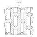
- FIG. 2is a plan view of the corrected mask pattern in FIG. 1;
- FIG. 3is a plan view illustrating the transfer of the corrected mask pattern to a photoresist layer
- FIG. 4is an enlarged plan view of part of FIG. 3;
- FIG. 5is a plan view illustrating the transfer of the uncorrected main mask pattern to the photoresist layer
- FIG. 6is an enlarged plan view of part of FIG. 5;
- FIG. 7is a plan view of a mask pattern illustrating a correction method according to a second embodiment of the invention.
- FIG. 8is a plan view of the corrected mask pattern in FIG. 7;
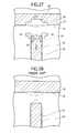
- FIG. 9is a plan view illustrating the transfer of the corrected mask pattern in FIG. 8 to a photoresist layer
- FIG. 10is an enlarged plan view of part of FIG. 9;
- FIG. 11is a plan view illustrating the transfer of the uncorrected main mask pattern in FIG. 7 to the photoresist layer;
- FIG. 12is an enlarged plan view of part of FIG. 11;
- FIG. 13is a plan view of a mask pattern illustrating a correction method according to a third embodiment of the invention.
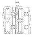
- FIG. 14is a plan view of the corrected mask pattern in FIG. 13;
- FIG. 15is a plan view illustrating the transfer of the corrected mask pattern in FIG. 14 to a photoresist layer
- FIG. 16is an enlarged plan view of part of FIG. 15;
- FIG. 17is a plan view illustrating the transfer of the uncorrected main mask pattern in FIG. 13 to the photoresist layer;
- FIG. 18is an enlarged plan view of part of FIG. 17;
- FIG. 19is a plan view of a mask pattern illustrating a correction method according to a fourth embodiment of the invention.
- FIG. 20is a plan view of the corrected mask pattern in FIG. 19;
- FIG. 21is a plan view illustrating the transfer of the corrected mask pattern in FIG. 20 to a photoresist layer
- FIG. 22is an enlarged plan view of part of FIG. 21;
- FIG. 23is a plan view illustrating the transfer of the uncorrected main mask pattern in FIG. 19 to the photoresist layer;
- FIG. 24is an enlarged plan view of part of FIG. 12;
- FIG. 25is a plan view of a mask pattern illustrating a correction method according to a fifth embodiment of the invention.
- FIG. 26is a plan view of the corrected mask pattern in FIG. 25;
- FIG. 27is a plan view illustrating the transfer of the corrected mask pattern in FIG. 26 to a photoresist layer.
- FIG. 28is a plan view illustrating the transfer of the uncorrected main mask pattern in FIG. 25 to the photoresist layer.
- a main mask patternis a pattern that defines the desired shape of a circuit element, line, or region.
- An outer serifis an extension of or addition to an opaque part of a main mask pattern.
- An inner serifis an indentation in or subtraction from an opaque part of the main mask pattern.
- the main mask pattern 10is a pattern of transparent rectangular slits.
- inner serifs 16are added at the corners 20 , 22 of the rectangular slits
- outer serifs 18are added at the ends 24 of the rectangular slits. More precisely, an outer serif 18 is added to each comparatively short edge 24 between adjacent corners 20 , 22 .
- the interior angle at the corners 20 , 22(the angle within the transparent area) is ninety degrees.
- the inner serif 16 and outer serif 18have a stepped shape, each comprising two steps. The serifs 16 , 18 alter the main mask pattern 10 to the corrected mask pattern 12 shown in FIG. 2.
- the added serifs 16 , 18produce an optical proximity correction (OPC) that brings the resist pattern 14 into close agreement with the main mask pattern 10 .
- OPCoptical proximity correction
- the inner serifs 16move the corners of the resist pattern 14 outward in the direction of the arrows marked A in FIG. 4, toward the corners 20 , 22 of the main mask pattern 10
- the outer serifs 18move the short edges of the resist pattern 14 inward, in the direction of arrow B, toward the short edges 24 of the main mask pattern 10 . Rounding of the resist at the corners 20 , 22 is thereby reduced.
- the two-step structure of the serifs 16 , 18operates as follows.
- the first step of each serifwhich is disposed directly adjacent to the main mask pattern 10 , corrects for the optical proximity effect (OPE) of the main mask pattern 10 , but produces an optical proximity effect of its own.
- the second step of the serifcorrects for the optical proximity effect of the first step, increasing the overall effectiveness of the correction.
- the number of stepsis not limited to two.
- the serifs 16 , 18may have three or more steps to achieve a still more effective optical proximity correction.
- FIGS. 5 and 6show the resist pattern 14 that would be formed by use of the uncorrected main mask pattern 10 , which is now indicated by solid lines.
- the resist pattern 14is rounded at the ends, and the active regions formed using the resist pattern 14 will be smaller than intended. Compared with these regions, the active regions formed using the corrected mask 12 in the first embodiment will have the desired size and the desired rectangular shape.
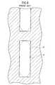
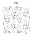
- the second embodimentreverses the transparency and opacity relationships of the first embodiment.
- the main mask pattern 10 in the second embodimentcomprises a plurality of opaque rectangles.
- the interior angles at the corners 20 , 22 of the opaque rectanglesare ninety degrees, these angles now being the angles in the opaque part of the mask pattern.
- the second embodimentadds inner serifs 16 to the short edges 24 of the opaque rectangles, and adds outer serifs 18 to the corners 20 , 22 of the opaque rectangles.
- the corrected mask pattern 12is shown in FIG. 8.
- the inner serifs 16bring the short edges of the rectangles in the resist pattern 14 inward, in the direction of arrow A in FIG. 10, and the outer serifs 18 move the corners of the resist pattern 14 outward, in the direction of the arrows marked B.
- the shape of the rectangles in the resist pattern 14closely follows the intended rectangular shape of the main mask pattern 10 .
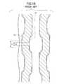
- FIGS. 11 and 12show the resist pattern 14 that would be formed by use of the uncorrected main mask pattern 10 , which is now indicated by solid lines.
- the resist pattern 14is rounded at the corners and ends, the rounded ends projecting considerably beyond the intended ends of the rectangles. Active regions formed using this resist pattern 14 will be larger than intended, and the spaces between facing ends of adjacent active regions will be more narrow than intended.
- the third embodimentwill be described in relation to the mask pattern of a photomask used to define the gates of transistors in a semiconductor ROM.
- the main mask pattern 10is a staggered pattern of transparent rectangles (or squares) linked by an overlapping pattern of long, thin parallel transparent slits.
- inner serifs 16are formed at the corners 20 , 22 of the transparent rectangles.
- the inner serifs 16have a single-step shape instead of a two-step shape.
- a two-step outer serif 18is formed on each complete edge 24 of each transparent rectangle, between the corners 20 , 22 .
- the corners 20 , 22have interior angles of ninety degrees, these being the angles within the transparent part of the mask pattern.
- the corrected mask pattern 12is shown in FIG. 14.
- the resulting resist pattern 14has the shape shown in FIGS. 15 and 16, including straight segments of length L 1 in the spaces between the transparent rectangles and of length L 2 at the interior edges of the transparent rectangles.
- the inner serifs 16push the corners of the resist pattern 14 outward, in the direction of the arrows marked A in FIG. 16, while the outer serif 18 pushes the edge between the corners in the opposite direction, indicated by arrow B.
- FIGS. 17 and 18show the resist pattern 14 that would be formed by the use of a main mask pattern 10 (now indicated by solid lines) that has not been corrected by the addition of serifs.
- This main mask pattern 10differs from the one in FIGS. 15 and 16 in that the corner angles differ from ninety degrees. Although the difference might be expected to affect mainly dimension L 1 , in fact, as shown in FIG. 18, both dimensions L 1 and L 2 are severely reduced, the straight segments of the resist pattern 14 becoming very short both within and between the transparent rectangles.
- the resist pattern 14has a highly rounded meandering shape, which is not suitable for the formation of transistor gates.
- the effect of the inner serifs and outer serifs in the third embodimentis similar to that in the preceding embodiments.
- the serifsinteract to reduce the rounding of the corners.
- the resist patternhas longer straight edges and follows the desired main mask pattern more closely. Gates of the desired width and length can be formed in the straight segments of the resist pattern.
- the corners 20 , 22 in FIGS. 13 to 16are not restricted to interior angles of ninety degrees, but the interior angles are preferably between forty-five degrees and one hundred thirty-five degrees.
- the fourth embodimentreverses the transparency and opacity relationships of the third embodiment.
- the main mask pattern 10 in the fourth embodimentis a pattern of parallel opaque lines with periodic rectangular (or square) widenings.
- Outer serifs 18are formed at the corners 20 , 22 of the rectangular widenings, and inner serifs 16 are formed at the edges of the rectangular widenings, between the corners 20 , 22 .
- the interior angles at the corners 20 , 22are ninety degrees (these being the angles in the opaque part of the pattern).
- the inner serifs 16now have two steps, while the outer serifs 18 have a single-step shape.
- the corrected mask pattern 12is shown in FIG. 20.
- the resulting resist pattern 14has the shape shown in FIGS. 21 and 22, including straight segments of length L 1 in the spaces between the rectangular widenings and of length L 2 at the outer edges of the rectangular widenings.
- the inner serifs 16push these latter edges inward, in the direction of arrow A in FIG. 22, while the outer serifs 18 push the corners outward, as indicated by the arrows marked B.
- the edges of the resist pattern 14are thereby brought closer to the intended edges of the main mask pattern 10 , increasing the lengths L 1 and L 2 of the straight segments of the resist pattern 14 .
- FIGS. 23 and 24show the resist pattern 14 that would be formed by use of a main mask pattern 10 (now indicated by solid lines) that has not been corrected by the addition of serifs, the corner angles being widened instead. As shown in FIG. 24, lengths L 1 and L 2 are reduced, as compared with FIG. 22, and the resist pattern 14 has a highly rounded shape.
- the main mask pattern in the fifth embodimentincludes an opaque line and another opaque region, one end of the opaque line facing a side of the opaque region.
- the other opaque regionis also a line.
- the main mask pattern 10is corrected by creating an inner serif 16 in the end 24 of the opaque line, and by adding two-step outer serifs 18 at the adjacent corners 20 , 22 of the opaque line, where the interior corner angles are ninety degrees.
- a two-step inner serif 16is created in the side 26 of the other opaque region, facing the end 24 of the opaque line.
- the corrected mask pattern 12is shown in FIG. 26.
- the serifs 16 , 18 added to the opaque linehave the same effect as in the second embodiment, pushing the corners of the resist pattern 14 outward in the direction of the arrows marked A and pulling the end of the resist pattern 14 inward, in the direction of arrow B, thereby reducing the rounding of the resist pattern 14 at the end of the line.
- the inner serif 16 created in the side of the opaque region facing the end of the opaque linepulls the resist pattern 14 in the direction of arrow C.
- the edges of the resist pattern 14closely follow the intended edges of the main mask pattern 10 , both at the end of the line and at the facing side.
- FIG. 28shows the resist pattern 14 that would be created by photolithography performed with a photomask having the uncorrected main mask pattern 10 . Due to the optical proximity effect, the end of the line is severely rounded, and the facing side of the other opaque region bulges out toward the end of the line, greatly reducing the distance between the end of the line and the facing side.
- the outer serifs 18 added at the corners 20 , 22 of the opaque line in the fifth embodimentdiffer slightly in shape from the outer serifs added in the second embodiment, to allow for the proximity of the facing side 26 of the other opaque region. As shown in FIG. 27, the result is an almost complete avoidance of any narrowing of the intended space between the two parts of the resist pattern 14 .
- a particular advantage of using the correction shown in the first or second embodiment for the photomask defining the active regions in a semiconductor device such as a ROMis that, since the rounding of the corners of the active regions is avoided, sufficient contact area is left even if transistor gates are situated near the edges of the active regions.
- the sizes of the circuit elements in the devicecan thus be reduced, circuit elements can be placed closer together, and higher levels of device integration can be attained without detriment to electrical characteristics.
- One way to reduce the size of a semiconductor device while avoiding unwanted contact between adjacent circuit elementsis to form gate electrodes in continuous swerving lines which are straight where the gates overlie the active regions, and swerve alternatively to one side and the other between the active regions. That is, the gate electrode lines follow paths with a crankshaft shape, although the angles at the bends are not limited to ninety degrees. If such gate lines are defined by a photomask with a main mask pattern corrected as in the third or fourth embodiment, the straight sections of the gate lines are lengthened and the lengths of the swerving sections between the straight sections are shortened, so that the active regions can be placed closer together while the straightness of the gate electrodes over the active regions is preserved. Integration levels can therefore be increased while adequate electrical characteristics are maintained.
- the invented correction methodis thus particularly effective when applied to the fabrication of a semiconductor device having patterns of active regions and gate lines of the general type illustrated in the first and third embodiments. As illustrated by the fifth embodiment, however, the effectiveness of the invented correction method is not restricted to gate lines and active regions.
- the inventionalso provides a photomask having a main mask pattern corrected by the adding serifs as described above, an exposure method including the use of this photomask, and a semiconductor device fabricated by a process employing the invented photomask for photolithography.
- the photomaskmay be used to define active regions of the semiconductor device, for example, or to define the gates of transistors.
Landscapes
- Physics & Mathematics (AREA)
- General Physics & Mathematics (AREA)
- Preparing Plates And Mask In Photomechanical Process (AREA)
- Exposure And Positioning Against Photoresist Photosensitive Materials (AREA)
Abstract
Description
- 1. Field of the Invention[0001]
- The present invention relates to a method of correcting the mask pattern of a photomask used in photolithography so as to obtain a desired resist pattern, to a photomask having the corrected mask pattern, to an exposure method using the photomask, and to a semiconductor device fabricated using the photomask.[0002]
- 2. Description of the Related Art[0003]
- Photolithography is a fundamental integrated circuit fabrication technique that transfers a pattern from a photomask (often referred to as a reticle) to a layer of photoresist. The pattern is transferred by exposing the photoresist layer to light through the photomask, then developed to form a resist mask.[0004]
- As integrated circuits reach ever-higher levels of integration, their shrinking internal dimensions, including both the sizes of circuit elements and the spacing between the circuit elements, pose problems for photolithography. One problem is the optical proximity effect (OPE), a general term for various phenomena that distort the mask pattern when it is transferred to the photoresist. For example, right-angled corners may become rounded, lines may become shortened at their ends, and line widths may be altered.[0005]
- These optical proximity effects can seriously alter the electrical characteristics of highly integrated circuits. They also affect fabrication yields, by causing unintended metal lines to overlap, for example, leading to short circuits and device failure.[0006]
- Known methods of compensating for optical proximity effects include the optical proximity corrections disclosed in U.S. Pat. No. 5,723,233 to Garza et al., and U.S. Pat. No. 5,879,844 to Yamamoto et al. These known methods include increasing the contrast of the exposure apparatus, expanding the process window, adding auxiliary patterns or serifs to the main mask pattern, and increasing or reducing the line widths in the main mask pattern.[0007]
- The known corrective methods, however, fail to provide a simple correction scheme adequate to the needs of current high levels of integration. There is a need for further corrective schemes.[0008]
- An object of the present invention is to provide a simple, effective method of correcting a main mask pattern used to create a resist pattern by photolithography.[0009]
- A more particular object is to improve the corner morphology of the resist pattern.[0010]
- In the invented method, first serifs are added to two adjacent corners of a part of the main mask pattern, and a second serif is added to an edge disposed between the two adjacent corners. The first and second serifs are of opposite type. If the part of the main mask pattern to which the serifs are added is a transparent part, the first serifs are inner serifs, increasing the transparent area, and the second serif is an outer serif, reducing the transparent area. If the part of the main mask pattern to which the serifs are added is an opaque part, the first serifs are outer serifs and the second serif is an inner serif.[0011]
- The corners to which the first serifs are added are preferably interior corners with angles of less than one hundred eighty degrees, more preferably with angles of from forty-five to one hundred thirty-five degrees. The edge to which the second serif is added is preferably shorter than other edges adjacent to the two corners. The second serif is preferably a multi-step serif. The first serifs may also have multiple steps.[0012]
- The two opposite types of serifs interact optically to improve the corner morphology of the resist pattern. In particular, corner rounding is reduced to a greater degree than by conventional methods.[0013]
- If the part of the main mask pattern to which the serifs are added is an opaque part, and the edge to which the second serif is added faces a side of another opaque part of the pattern, an inner serif is preferably added to that side, facing the second serif. This inner serif prevents the side from bulging due to an optical proximity effect.[0014]
- In the attached drawings:[0015]
- FIG. 1 is a plan view of a mask pattern illustrating a correction method according to a first embodiment of the invention;[0016]
- FIG. 2 is a plan view of the corrected mask pattern in FIG. 1;[0017]
- FIG. 3 is a plan view illustrating the transfer of the corrected mask pattern to a photoresist layer;[0018]
- FIG. 4 is an enlarged plan view of part of FIG. 3;[0019]
- FIG. 5 is a plan view illustrating the transfer of the uncorrected main mask pattern to the photoresist layer;[0020]
- FIG. 6 is an enlarged plan view of part of FIG. 5;[0021]
- FIG. 7 is a plan view of a mask pattern illustrating a correction method according to a second embodiment of the invention;[0022]
- FIG. 8 is a plan view of the corrected mask pattern in FIG. 7;[0023]
- FIG. 9 is a plan view illustrating the transfer of the corrected mask pattern in FIG. 8 to a photoresist layer;[0024]
- FIG. 10 is an enlarged plan view of part of FIG. 9;[0025]
- FIG. 11 is a plan view illustrating the transfer of the uncorrected main mask pattern in FIG. 7 to the photoresist layer;[0026]
- FIG. 12 is an enlarged plan view of part of FIG. 11;[0027]
- FIG. 13 is a plan view of a mask pattern illustrating a correction method according to a third embodiment of the invention;[0028]
- FIG. 14 is a plan view of the corrected mask pattern in FIG. 13;[0029]
- FIG. 15 is a plan view illustrating the transfer of the corrected mask pattern in FIG. 14 to a photoresist layer;[0030]
- FIG. 16 is an enlarged plan view of part of FIG. 15;[0031]
- FIG. 17 is a plan view illustrating the transfer of the uncorrected main mask pattern in FIG. 13 to the photoresist layer;[0032]
- FIG. 18 is an enlarged plan view of part of FIG. 17;[0033]
- FIG. 19 is a plan view of a mask pattern illustrating a correction method according to a fourth embodiment of the invention;[0034]
- FIG. 20 is a plan view of the corrected mask pattern in FIG. 19;[0035]
- FIG. 21 is a plan view illustrating the transfer of the corrected mask pattern in FIG. 20 to a photoresist layer;[0036]
- FIG. 22 is an enlarged plan view of part of FIG. 21;[0037]
- FIG. 23 is a plan view illustrating the transfer of the uncorrected main mask pattern in FIG. 19 to the photoresist layer;[0038]
- FIG. 24 is an enlarged plan view of part of FIG. 12;[0039]
- FIG. 25 is a plan view of a mask pattern illustrating a correction method according to a fifth embodiment of the invention;[0040]
- FIG. 26 is a plan view of the corrected mask pattern in FIG. 25;[0041]
- FIG. 27 is a plan view illustrating the transfer of the corrected mask pattern in FIG. 26 to a photoresist layer; and[0042]
- FIG. 28 is a plan view illustrating the transfer of the uncorrected main mask pattern in FIG. 25 to the photoresist layer.[0043]
- Embodiments of the invention will now be described with reference to the attached drawings, in which like elements are indicated by like reference characters. Throughout the drawings, dashed lines will indicate an uncorrected main mask pattern, solid lines will indicate a mask pattern actually formed on a photomask, dash-dot lines with double dots will indicate a resist pattern, hatching will indicate opaque parts of the photomask, and white areas will indicate transparent parts of the photomask.[0044]
- The terms ‘main mask pattern’, ‘inner serif’, and ‘outer serif’ will be used as follows. A main mask pattern is a pattern that defines the desired shape of a circuit element, line, or region. An outer serif is an extension of or addition to an opaque part of a main mask pattern. An inner serif is an indentation in or subtraction from an opaque part of the main mask pattern.[0045]
- The first embodiment will be described in relation to the fabrication of a semiconductor device such as a read-only memory (ROM), and more particularly in relation to a photomask used to define the active regions of the device. Referring to FIG. 1, the[0046]
main mask pattern 10 is a pattern of transparent rectangular slits. In the first embodiment,inner serifs 16 are added at thecorners outer serifs 18 are added at theends 24 of the rectangular slits. More precisely, anouter serif 18 is added to each comparativelyshort edge 24 betweenadjacent corners corners 20,22 (the angle within the transparent area) is ninety degrees. Theinner serif 16 andouter serif 18 have a stepped shape, each comprising two steps. Theserifs main mask pattern 10 to the correctedmask pattern 12 shown in FIG. 2. - Referring to FIGS. 3 and 4, when photolithography is performed using a photomask having the corrected[0047]
mask pattern 12, the addedserifs pattern 14 into close agreement with themain mask pattern 10. Specifically, theinner serifs 16 move the corners of the resistpattern 14 outward in the direction of the arrows marked A in FIG. 4, toward thecorners main mask pattern 10, and theouter serifs 18 move the short edges of the resistpattern 14 inward, in the direction of arrow B, toward theshort edges 24 of themain mask pattern 10. Rounding of the resist at thecorners - The two-step structure of the[0048]
serifs main mask pattern 10, corrects for the optical proximity effect (OPE) of themain mask pattern 10, but produces an optical proximity effect of its own. The second step of the serif corrects for the optical proximity effect of the first step, increasing the overall effectiveness of the correction. - Although at least two steps are preferable, the number of steps is not limited to two. The[0049]
serifs - FIGS. 5 and 6 show the resist[0050]
pattern 14 that would be formed by use of the uncorrectedmain mask pattern 10, which is now indicated by solid lines. The resistpattern 14 is rounded at the ends, and the active regions formed using the resistpattern 14 will be smaller than intended. Compared with these regions, the active regions formed using the correctedmask 12 in the first embodiment will have the desired size and the desired rectangular shape. - The second embodiment reverses the transparency and opacity relationships of the first embodiment. Referring to FIG. 7, the[0051]
main mask pattern 10 in the second embodiment comprises a plurality of opaque rectangles. The interior angles at thecorners inner serifs 16 to theshort edges 24 of the opaque rectangles, and addsouter serifs 18 to thecorners mask pattern 12 is shown in FIG. 8. - Referring to FIGS. 9 and 10, when photolithography is performed using a photomask having the corrected[0052]
mask pattern 12 of the second embodiment, theinner serifs 16 bring the short edges of the rectangles in the resistpattern 14 inward, in the direction of arrow A in FIG. 10, and theouter serifs 18 move the corners of the resistpattern 14 outward, in the direction of the arrows marked B. As a result, the shape of the rectangles in the resistpattern 14 closely follows the intended rectangular shape of themain mask pattern 10. - FIGS. 11 and 12 show the resist[0053]
pattern 14 that would be formed by use of the uncorrectedmain mask pattern 10, which is now indicated by solid lines. The resistpattern 14 is rounded at the corners and ends, the rounded ends projecting considerably beyond the intended ends of the rectangles. Active regions formed using this resistpattern 14 will be larger than intended, and the spaces between facing ends of adjacent active regions will be more narrow than intended. - The third embodiment will be described in relation to the mask pattern of a photomask used to define the gates of transistors in a semiconductor ROM. Referring to FIG. 13, the[0054]
main mask pattern 10 is a staggered pattern of transparent rectangles (or squares) linked by an overlapping pattern of long, thin parallel transparent slits. To correct the mask pattern,inner serifs 16 are formed at thecorners inner serifs 16 have a single-step shape instead of a two-step shape. A two-stepouter serif 18 is formed on eachcomplete edge 24 of each transparent rectangle, between thecorners corners mask pattern 12 is shown in FIG. 14. - When photolithography is performed using a photomask with the corrected[0055]
mask pattern 12 in the third embodiment, the resulting resistpattern 14 has the shape shown in FIGS. 15 and 16, including straight segments of length L1 in the spaces between the transparent rectangles and of length L2 at the interior edges of the transparent rectangles. As in the preceding embodiments, theinner serifs 16 push the corners of the resistpattern 14 outward, in the direction of the arrows marked A in FIG. 16, while theouter serif 18 pushes the edge between the corners in the opposite direction, indicated by arrow B. - FIGS. 17 and 18 show the resist[0056]
pattern 14 that would be formed by the use of a main mask pattern10 (now indicated by solid lines) that has not been corrected by the addition of serifs. Thismain mask pattern 10 differs from the one in FIGS. 15 and 16 in that the corner angles differ from ninety degrees. Although the difference might be expected to affect mainly dimension L1, in fact, as shown in FIG. 18, both dimensions L1 and L2 are severely reduced, the straight segments of the resistpattern 14 becoming very short both within and between the transparent rectangles. The resistpattern 14 has a highly rounded meandering shape, which is not suitable for the formation of transistor gates. - The effect of the inner serifs and outer serifs in the third embodiment is similar to that in the preceding embodiments. The serifs interact to reduce the rounding of the corners. As a result, the resist pattern has longer straight edges and follows the desired main mask pattern more closely. Gates of the desired width and length can be formed in the straight segments of the resist pattern.[0057]
- The[0058]
corners - The fourth embodiment reverses the transparency and opacity relationships of the third embodiment. Referring to FIG. 19, the[0059]
main mask pattern 10 in the fourth embodiment is a pattern of parallel opaque lines with periodic rectangular (or square) widenings.Outer serifs 18 are formed at thecorners inner serifs 16 are formed at the edges of the rectangular widenings, between thecorners corners inner serifs 16 now have two steps, while theouter serifs 18 have a single-step shape. The correctedmask pattern 12 is shown in FIG. 20. - When photolithography is performed using a photomask with the corrected[0060]
mask pattern 12 in the fourth embodiment, the resulting resistpattern 14 has the shape shown in FIGS. 21 and 22, including straight segments of length L1 in the spaces between the rectangular widenings and of length L2 at the outer edges of the rectangular widenings. Theinner serifs 16 push these latter edges inward, in the direction of arrow A in FIG. 22, while theouter serifs 18 push the corners outward, as indicated by the arrows marked B. The edges of the resistpattern 14 are thereby brought closer to the intended edges of themain mask pattern 10, increasing the lengths L1 and L2 of the straight segments of the resistpattern 14. - FIGS. 23 and 24 show the resist[0061]
pattern 14 that would be formed by use of a main mask pattern10 (now indicated by solid lines) that has not been corrected by the addition of serifs, the corner angles being widened instead. As shown in FIG. 24, lengths L1 and L2 are reduced, as compared with FIG. 22, and the resistpattern 14 has a highly rounded shape. - The effect of the inner serifs and outer serifs in the fourth embodiment is similar to that in the preceding embodiments, reducing the rounding of the corners and producing a resist pattern with longer straight edges.[0062]
- The main mask pattern in the fifth embodiment includes an opaque line and another opaque region, one end of the opaque line facing a side of the opaque region. In FIG. 25, the other opaque region is also a line. The[0063]
main mask pattern 10 is corrected by creating aninner serif 16 in theend 24 of the opaque line, and by adding two-stepouter serifs 18 at theadjacent corners inner serif 16 is created in theside 26 of the other opaque region, facing theend 24 of the opaque line. The correctedmask pattern 12 is shown in FIG. 26. - Referring to FIG. 27, when photolithography is performed with a photomask having the corrected[0064]
mask pattern 12, theserifs pattern 14 outward in the direction of the arrows marked A and pulling the end of the resistpattern 14 inward, in the direction of arrow B, thereby reducing the rounding of the resistpattern 14 at the end of the line. In addition, theinner serif 16 created in the side of the opaque region facing the end of the opaque line pulls the resistpattern 14 in the direction of arrow C. As a result, the edges of the resistpattern 14 closely follow the intended edges of themain mask pattern 10, both at the end of the line and at the facing side. - FIG. 28 shows the resist[0065]
pattern 14 that would be created by photolithography performed with a photomask having the uncorrectedmain mask pattern 10. Due to the optical proximity effect, the end of the line is severely rounded, and the facing side of the other opaque region bulges out toward the end of the line, greatly reducing the distance between the end of the line and the facing side. - The[0066]
outer serifs 18 added at thecorners side 26 of the other opaque region. As shown in FIG. 27, the result is an almost complete avoidance of any narrowing of the intended space between the two parts of the resistpattern 14. - When semiconductor devices are fabricated, if the method of the present invention is used to correct the main mask patterns of photomasks used in the photolithography steps in the fabrication process, resist patterns closely following the intended patterns are created. Benefits include increased yield of the fabrication process, and improved electrical characteristics of the integrated circuits in the fabricated semiconductor devices.[0067]
- A particular advantage of using the correction shown in the first or second embodiment for the photomask defining the active regions in a semiconductor device such as a ROM is that, since the rounding of the corners of the active regions is avoided, sufficient contact area is left even if transistor gates are situated near the edges of the active regions. The sizes of the circuit elements in the device can thus be reduced, circuit elements can be placed closer together, and higher levels of device integration can be attained without detriment to electrical characteristics.[0068]
- One way to reduce the size of a semiconductor device while avoiding unwanted contact between adjacent circuit elements is to form gate electrodes in continuous swerving lines which are straight where the gates overlie the active regions, and swerve alternatively to one side and the other between the active regions. That is, the gate electrode lines follow paths with a crankshaft shape, although the angles at the bends are not limited to ninety degrees. If such gate lines are defined by a photomask with a main mask pattern corrected as in the third or fourth embodiment, the straight sections of the gate lines are lengthened and the lengths of the swerving sections between the straight sections are shortened, so that the active regions can be placed closer together while the straightness of the gate electrodes over the active regions is preserved. Integration levels can therefore be increased while adequate electrical characteristics are maintained.[0069]
- The invented correction method is thus particularly effective when applied to the fabrication of a semiconductor device having patterns of active regions and gate lines of the general type illustrated in the first and third embodiments. As illustrated by the fifth embodiment, however, the effectiveness of the invented correction method is not restricted to gate lines and active regions.[0070]
- The invention is not limited to the corrections shown as examples in the preceding embodiments. The shapes of the serifs and the numbers of steps can be varied, as mentioned above, and those skilled in the art will recognize that further variations are possible within the scope of the appended claims.[0071]
- The invention also provides a photomask having a main mask pattern corrected by the adding serifs as described above, an exposure method including the use of this photomask, and a semiconductor device fabricated by a process employing the invented photomask for photolithography. The photomask may be used to define active regions of the semiconductor device, for example, or to define the gates of transistors.[0072]
Claims (11)
1. A method of correcting a main mask pattern used to create a resist pattern by photolithography, to improve the corner morphology of the resist pattern, comprising:
adding first serifs to two adjacent corners of a part of the mask pattern; and
adding a second serif to an edge of said part of the mask pattern disposed between said two adjacent corners, the second serif being opposite in type to the first serifs.
2. The method ofclaim 1 , wherein said part of the mask pattern is transparent, said first serifs are inner serifs, and said second serif is an outer serif.
3. The method ofclaim 2 , wherein said corners have interior angles less than one hundred eighty degrees.
4. The method ofclaim 3 , wherein said corners have interior angles of from forty-five degrees to one hundred thirty-five degrees.
5. The method ofclaim 1 , wherein said part of the mask pattern is opaque, said first serifs are outer serifs, and said second serif is an inner serif.
6. The method ofclaim 5 , wherein said corners have interior angles less than one hundred eighty degrees.
7. The method ofclaim 6 , wherein said corners have interior angles of from forty-five degrees to one hundred thirty-five degrees.
8. The method ofclaim 6 , wherein said main mask pattern has another opaque part with a side facing said edge, the method further comprising adding an inner serif to said side, facing the inner serif added to said edge.
9. The method ofclaim 1 , wherein said edge is shorter than other edges of said part of said main mask pattern adjacent to said corners.
10. The method ofclaim 1 , wherein said first serifs are multi-step serifs.
11. The method ofclaim 1 , wherein said second serif is a multi-step serif.
Applications Claiming Priority (2)
| Application Number | Priority Date | Filing Date | Title |
|---|---|---|---|
| JP2002-053378 | 2002-02-28 | ||
| JP2002053378AJP2003255508A (en) | 2002-02-28 | 2002-02-28 | Correction method for mask pattern, photomask, exposure method and semiconductor device |
Publications (2)
| Publication Number | Publication Date |
|---|---|
| US20030162103A1true US20030162103A1 (en) | 2003-08-28 |
| US6869738B2 US6869738B2 (en) | 2005-03-22 |
Family
ID=27750915
Family Applications (1)
| Application Number | Title | Priority Date | Filing Date |
|---|---|---|---|
| US10/305,098Expired - LifetimeUS6869738B2 (en) | 2002-02-28 | 2002-11-27 | Mask pattern correction method |
Country Status (2)
| Country | Link |
|---|---|
| US (1) | US6869738B2 (en) |
| JP (1) | JP2003255508A (en) |
Cited By (12)
| Publication number | Priority date | Publication date | Assignee | Title |
|---|---|---|---|---|
| US20050250020A1 (en)* | 2004-05-07 | 2005-11-10 | Mosel Vitelic, Inc. | Mask, layout thereon and method therefor |
| US20080028359A1 (en)* | 2006-07-31 | 2008-01-31 | Stefan Blawid | Termination structure, a mask for manufacturing a termination structure, a lithographic process and a semiconductor device with a termination structure |
| US20130009275A1 (en)* | 2010-05-17 | 2013-01-10 | Panasonic Corporation | Semiconductor integrated circuit device and terminal structure of standard cell |
| US8589830B2 (en)* | 2012-03-07 | 2013-11-19 | Taiwan Semiconductor Manufacturing Company, Ltd. | Method and apparatus for enhanced optical proximity correction |
| CN106019815A (en)* | 2016-07-13 | 2016-10-12 | 武汉华星光电技术有限公司 | Photomask with exposure correction function |
| CN106200257A (en)* | 2016-07-13 | 2016-12-07 | 武汉华星光电技术有限公司 | A kind of light shield with exposure correction |
| US10042245B2 (en) | 2016-07-13 | 2018-08-07 | Wuhan China Star Optoelectronics Technology Co., Ltd. | Photomask having an exposure correction function |
| DE102017120185A1 (en)* | 2017-08-25 | 2019-02-28 | Taiwan Semiconductor Manufacturing Co. Ltd. | Method and integrated circuit design with non-linear busbars |
| CN109407430A (en)* | 2018-12-17 | 2019-03-01 | 武汉华星光电技术有限公司 | A kind of array substrate and preparation method thereof |
| CN110068951A (en)* | 2019-01-15 | 2019-07-30 | 东旭(昆山)显示材料有限公司 | Picture element light shield, the method for producing display and display |
| US20220414309A1 (en)* | 2021-06-25 | 2022-12-29 | Taiwan Semiconductor Manufacturing Company, Ltd. | Method and structure for mandrel patterning |
| US20230010293A1 (en)* | 2021-07-12 | 2023-01-12 | Changxin Memory Technologies, Inc. | Semiconductor integrated circuit design method and apparatus |
Families Citing this family (16)
| Publication number | Priority date | Publication date | Assignee | Title |
|---|---|---|---|---|
| US7010764B2 (en)* | 2003-04-14 | 2006-03-07 | Takumi Technology Corp. | Effective proximity effect correction methodology |
| JP4561173B2 (en)* | 2004-05-11 | 2010-10-13 | セイコーエプソン株式会社 | ELECTRO-OPTICAL DEVICE, MANUFACTURING METHOD THEREOF, AND ELECTRONIC DEVICE |
| US20060292885A1 (en)* | 2005-06-24 | 2006-12-28 | Texas Instruments Incorporated | Layout modification to eliminate line bending caused by line material shrinkage |
| KR100645534B1 (en) | 2005-08-12 | 2006-11-14 | 삼성에스디아이 주식회사 | Laser thermal transfer mask and manufacturing method of organic electroluminescent device using same |
| KR100815957B1 (en)* | 2006-09-06 | 2008-03-21 | 동부일렉트로닉스 주식회사 | Photo mask |
| KR100880229B1 (en)* | 2007-05-23 | 2009-01-28 | 주식회사 동부하이텍 | Method of manufacturing mask of semiconductor device |
| US20090108305A1 (en)* | 2007-10-30 | 2009-04-30 | Riviere-Cazaux Lionel J | Semiconductor having a corner compensation feature and method |
| JP5173701B2 (en)* | 2008-09-25 | 2013-04-03 | パナソニック株式会社 | Method for forming wiring pattern of printed wiring board and method for manufacturing printed wiring board |
| KR101015533B1 (en)* | 2008-10-14 | 2011-02-16 | 주식회사 동부하이텍 | Exposure mask for forming photodiode and manufacturing method of image sensor using same |
| US7944545B2 (en)* | 2009-05-11 | 2011-05-17 | International Business Machines Corporation | High contrast lithographic masks |
| JP2011248347A (en)* | 2010-04-28 | 2011-12-08 | Semiconductor Energy Lab Co Ltd | Photomask |
| US8323857B2 (en) | 2010-12-21 | 2012-12-04 | Ultratech, Inc. | Phase-shift mask with assist phase regions |
| KR101949412B1 (en) | 2011-05-24 | 2019-02-19 | 삼성디스플레이 주식회사 | Photoresist pattern and method for the same |
| KR101958355B1 (en) | 2012-05-22 | 2019-07-03 | 삼성디스플레이 주식회사 | Mask with assist pattern |
| JP6833430B2 (en)* | 2016-09-27 | 2021-02-24 | 東芝情報システム株式会社 | Manufacturing method of solid-state image sensor |
| US10838295B2 (en)* | 2017-05-04 | 2020-11-17 | Taiwan Semiconductor Manufacturing Company, Ltd. | Photomask and fabrication method therefor |
Citations (6)
| Publication number | Priority date | Publication date | Assignee | Title |
|---|---|---|---|---|
| US5723233A (en)* | 1996-02-27 | 1998-03-03 | Lsi Logic Corporation | Optical proximity correction method and apparatus |
| US5879844A (en)* | 1995-12-22 | 1999-03-09 | Kabushiki Kaisha Toshiba | Optical proximity correction method |
| US5991006A (en)* | 1996-10-29 | 1999-11-23 | Sony Corporation | Method and apparatus for correcting exposure patterns, and exposure mask, method of exposing and semiconductor device |
| US6044007A (en)* | 1999-03-24 | 2000-03-28 | Advanced Micro Devices, Inc. | Modification of mask layout data to improve writeability of OPC |
| US6168891B1 (en)* | 1998-11-30 | 2001-01-02 | Matsushita Electric Industrial Co., Ltd. | Method for correcting mask pattern for use in manufacturing of semiconductor integrated circuit |
| US6501083B1 (en)* | 1999-11-01 | 2002-12-31 | Nikon Corporation | Methods for calculating cumulative dose of exposure energy from regions of a microlithography reticle for use in correcting proximity effects |
Family Cites Families (5)
| Publication number | Priority date | Publication date | Assignee | Title |
|---|---|---|---|---|
| JP3409493B2 (en) | 1995-03-13 | 2003-05-26 | ソニー株式会社 | Mask pattern correction method and correction device |
| JP3331822B2 (en) | 1995-07-17 | 2002-10-07 | ソニー株式会社 | Mask pattern correction method, mask using the same, exposure method, and semiconductor device |
| JP2000031021A (en) | 1998-07-14 | 2000-01-28 | Hitachi Ltd | Reflective mask and device manufacturing method using the same |
| JP2000235251A (en) | 1999-02-16 | 2000-08-29 | Sony Corp | Exposure pattern correction method, exposure method, aligner, photomask and semiconductor device |
| JP2000330258A (en) | 1999-05-20 | 2000-11-30 | United Microelectronics Corp | Optical proximity correction method |
- 2002
- 2002-02-28JPJP2002053378Apatent/JP2003255508A/enactivePending
- 2002-11-27USUS10/305,098patent/US6869738B2/ennot_activeExpired - Lifetime
Patent Citations (6)
| Publication number | Priority date | Publication date | Assignee | Title |
|---|---|---|---|---|
| US5879844A (en)* | 1995-12-22 | 1999-03-09 | Kabushiki Kaisha Toshiba | Optical proximity correction method |
| US5723233A (en)* | 1996-02-27 | 1998-03-03 | Lsi Logic Corporation | Optical proximity correction method and apparatus |
| US5991006A (en)* | 1996-10-29 | 1999-11-23 | Sony Corporation | Method and apparatus for correcting exposure patterns, and exposure mask, method of exposing and semiconductor device |
| US6168891B1 (en)* | 1998-11-30 | 2001-01-02 | Matsushita Electric Industrial Co., Ltd. | Method for correcting mask pattern for use in manufacturing of semiconductor integrated circuit |
| US6044007A (en)* | 1999-03-24 | 2000-03-28 | Advanced Micro Devices, Inc. | Modification of mask layout data to improve writeability of OPC |
| US6501083B1 (en)* | 1999-11-01 | 2002-12-31 | Nikon Corporation | Methods for calculating cumulative dose of exposure energy from regions of a microlithography reticle for use in correcting proximity effects |
Cited By (20)
| Publication number | Priority date | Publication date | Assignee | Title |
|---|---|---|---|---|
| US20050250020A1 (en)* | 2004-05-07 | 2005-11-10 | Mosel Vitelic, Inc. | Mask, layout thereon and method therefor |
| US20080028359A1 (en)* | 2006-07-31 | 2008-01-31 | Stefan Blawid | Termination structure, a mask for manufacturing a termination structure, a lithographic process and a semiconductor device with a termination structure |
| US20130009275A1 (en)* | 2010-05-17 | 2013-01-10 | Panasonic Corporation | Semiconductor integrated circuit device and terminal structure of standard cell |
| US8589830B2 (en)* | 2012-03-07 | 2013-11-19 | Taiwan Semiconductor Manufacturing Company, Ltd. | Method and apparatus for enhanced optical proximity correction |
| CN106019815A (en)* | 2016-07-13 | 2016-10-12 | 武汉华星光电技术有限公司 | Photomask with exposure correction function |
| CN106200257A (en)* | 2016-07-13 | 2016-12-07 | 武汉华星光电技术有限公司 | A kind of light shield with exposure correction |
| WO2018010228A1 (en)* | 2016-07-13 | 2018-01-18 | 武汉华星光电技术有限公司 | Photo mask with exposure compensation function |
| WO2018010227A1 (en)* | 2016-07-13 | 2018-01-18 | 武汉华星光电技术有限公司 | Photo mask with exposure compensation function |
| US10042245B2 (en) | 2016-07-13 | 2018-08-07 | Wuhan China Star Optoelectronics Technology Co., Ltd. | Photomask having an exposure correction function |
| US11581221B2 (en) | 2017-08-25 | 2023-02-14 | Taiwan Semiconductor Manufacturing Co., Ltd | Method and IC design with non-linear power rails |
| US10515850B2 (en) | 2017-08-25 | 2019-12-24 | Taiwan Semiconductor Manufacturing Co., Ltd. | Method and IC design with non-linear power rails |
| DE102017120185A1 (en)* | 2017-08-25 | 2019-02-28 | Taiwan Semiconductor Manufacturing Co. Ltd. | Method and integrated circuit design with non-linear busbars |
| US11996329B2 (en) | 2017-08-25 | 2024-05-28 | Taiwan Semiconductor Manufacturing Co., Ltd. | Method and IC design with non-linear power rails |
| DE102017120185B4 (en)* | 2017-08-25 | 2025-07-10 | Taiwan Semiconductor Manufacturing Co. Ltd. | Method and integrated circuit design with nonlinear power rails |
| CN109407430A (en)* | 2018-12-17 | 2019-03-01 | 武汉华星光电技术有限公司 | A kind of array substrate and preparation method thereof |
| CN110068951A (en)* | 2019-01-15 | 2019-07-30 | 东旭(昆山)显示材料有限公司 | Picture element light shield, the method for producing display and display |
| US20220414309A1 (en)* | 2021-06-25 | 2022-12-29 | Taiwan Semiconductor Manufacturing Company, Ltd. | Method and structure for mandrel patterning |
| US12073166B2 (en)* | 2021-06-25 | 2024-08-27 | Taiwan Semiconductor Manufacturing Company, Ltd. | Method and structure for mandrel patterning |
| US20230010293A1 (en)* | 2021-07-12 | 2023-01-12 | Changxin Memory Technologies, Inc. | Semiconductor integrated circuit design method and apparatus |
| US12242791B2 (en)* | 2021-07-12 | 2025-03-04 | Changxin Memory Technologies, Inc. | Semiconductor integrated circuit design method and apparatus |
Also Published As
| Publication number | Publication date |
|---|---|
| US6869738B2 (en) | 2005-03-22 |
| JP2003255508A (en) | 2003-09-10 |
Similar Documents
| Publication | Publication Date | Title |
|---|---|---|
| US6869738B2 (en) | Mask pattern correction method | |
| JP3327394B2 (en) | Optical proximity correction method | |
| KR100589041B1 (en) | Mask and Formation Method | |
| US20130275928A1 (en) | Method for correcting layout pattern and mask thereof | |
| CN107490932B (en) | Method for correcting mask graph | |
| US7939225B2 (en) | Mask for controlling line end shortening and corner rounding arising from proximity effects | |
| US8071264B2 (en) | Pattern formation method using levenson-type mask and method of manufacturing levenson-type mask | |
| US7419767B2 (en) | Phase-shifting mask and method of forming pattern using the same | |
| JP3751907B2 (en) | Alternating phase shift mask | |
| JP2008130897A (en) | Integrated circuit pattern layout | |
| US20090001596A1 (en) | Conductive line structure | |
| US6861178B2 (en) | Phase shift mask, method of exposure, and method of producing semiconductor device | |
| US7341808B2 (en) | Method and system for contiguous proximity correction for semiconductor masks | |
| KR100549268B1 (en) | Phase inversion mask and manufacturing method thereof | |
| KR100465067B1 (en) | Photo mask, method of manufacturing the same and method of forming a photosensitive film pattern of using the same | |
| TWI880530B (en) | Photomask for semiconductor manufacturing and method for modifying photomask pattern | |
| KR100462887B1 (en) | A phase edge phase shift mask enforcing a field gate image and a fabrication method thereof | |
| US7544446B2 (en) | Masks of semiconductor devices and methods of forming patterns thereof | |
| US6335125B2 (en) | Photomask and method of manufacturing same | |
| JP2007123342A (en) | Manufacturing method of semiconductor device | |
| KR100443518B1 (en) | Method of manufacturing dram cell transistor | |
| KR100434707B1 (en) | Exposure mask for semiconductor device manufacture | |
| KR20020014598A (en) | Method of defining patterns in a semiconductor device | |
| JP2002006477A (en) | Method for modifying pattern shape of photomask and modified photomask | |
| KR100529623B1 (en) | A method for forming a mask pattern of a semiconductor device |
Legal Events
| Date | Code | Title | Description |
|---|---|---|---|
| AS | Assignment | Owner name:OKI ELECTRIC INDUSTRY CO., LTD., JAPAN Free format text:ASSIGNMENT OF ASSIGNORS INTEREST;ASSIGNORS:OSHIMA, KATSUO;MUTO, KOKI;REEL/FRAME:013533/0482 Effective date:20021107 | |
| FEPP | Fee payment procedure | Free format text:PAYOR NUMBER ASSIGNED (ORIGINAL EVENT CODE: ASPN); ENTITY STATUS OF PATENT OWNER: LARGE ENTITY | |
| STCF | Information on status: patent grant | Free format text:PATENTED CASE | |
| FPAY | Fee payment | Year of fee payment:4 | |
| AS | Assignment | Owner name:OKI SEMICONDUCTOR CO., LTD., JAPAN Free format text:CHANGE OF NAME;ASSIGNOR:OKI ELECTRIC INDUSTRY CO., LTD.;REEL/FRAME:022052/0540 Effective date:20081001 | |
| FPAY | Fee payment | Year of fee payment:8 | |
| AS | Assignment | Owner name:LAPIS SEMICONDUCTOR CO., LTD., JAPAN Free format text:CHANGE OF NAME;ASSIGNOR:OKI SEMICONDUCTOR CO., LTD;REEL/FRAME:032495/0483 Effective date:20111003 | |
| FPAY | Fee payment | Year of fee payment:12 |