US20030160325A1 - Semiconductor device substrate and manufacturing method thereof and semiconductor package - Google Patents
Semiconductor device substrate and manufacturing method thereof and semiconductor packageDownload PDFInfo
- Publication number
- US20030160325A1 US20030160325A1US10/262,074US26207402AUS2003160325A1US 20030160325 A1US20030160325 A1US 20030160325A1US 26207402 AUS26207402 AUS 26207402AUS 2003160325 A1US2003160325 A1US 2003160325A1
- Authority
- US
- United States
- Prior art keywords
- silicon substrate
- semiconductor device
- substrate
- mounting terminal
- device substrate
- Prior art date
- Legal status (The legal status is an assumption and is not a legal conclusion. Google has not performed a legal analysis and makes no representation as to the accuracy of the status listed.)
- Granted
Links
Images


Classifications
- H—ELECTRICITY
- H01—ELECTRIC ELEMENTS
- H01L—SEMICONDUCTOR DEVICES NOT COVERED BY CLASS H10
- H01L21/00—Processes or apparatus adapted for the manufacture or treatment of semiconductor or solid state devices or of parts thereof
- H01L21/67—Apparatus specially adapted for handling semiconductor or electric solid state devices during manufacture or treatment thereof; Apparatus specially adapted for handling wafers during manufacture or treatment of semiconductor or electric solid state devices or components ; Apparatus not specifically provided for elsewhere
- H01L21/683—Apparatus specially adapted for handling semiconductor or electric solid state devices during manufacture or treatment thereof; Apparatus specially adapted for handling wafers during manufacture or treatment of semiconductor or electric solid state devices or components ; Apparatus not specifically provided for elsewhere for supporting or gripping
- H01L21/6835—Apparatus specially adapted for handling semiconductor or electric solid state devices during manufacture or treatment thereof; Apparatus specially adapted for handling wafers during manufacture or treatment of semiconductor or electric solid state devices or components ; Apparatus not specifically provided for elsewhere for supporting or gripping using temporarily an auxiliary support
- H—ELECTRICITY
- H01—ELECTRIC ELEMENTS
- H01L—SEMICONDUCTOR DEVICES NOT COVERED BY CLASS H10
- H01L23/00—Details of semiconductor or other solid state devices
- H01L23/12—Mountings, e.g. non-detachable insulating substrates
- H—ELECTRICITY
- H01—ELECTRIC ELEMENTS
- H01L—SEMICONDUCTOR DEVICES NOT COVERED BY CLASS H10
- H01L21/00—Processes or apparatus adapted for the manufacture or treatment of semiconductor or solid state devices or of parts thereof
- H01L21/02—Manufacture or treatment of semiconductor devices or of parts thereof
- H01L21/04—Manufacture or treatment of semiconductor devices or of parts thereof the devices having potential barriers, e.g. a PN junction, depletion layer or carrier concentration layer
- H01L21/48—Manufacture or treatment of parts, e.g. containers, prior to assembly of the devices, using processes not provided for in a single one of the groups H01L21/18 - H01L21/326 or H10D48/04 - H10D48/07
- H01L21/4814—Conductive parts
- H01L21/4846—Leads on or in insulating or insulated substrates, e.g. metallisation
- H—ELECTRICITY
- H01—ELECTRIC ELEMENTS
- H01L—SEMICONDUCTOR DEVICES NOT COVERED BY CLASS H10
- H01L21/00—Processes or apparatus adapted for the manufacture or treatment of semiconductor or solid state devices or of parts thereof
- H01L21/02—Manufacture or treatment of semiconductor devices or of parts thereof
- H01L21/04—Manufacture or treatment of semiconductor devices or of parts thereof the devices having potential barriers, e.g. a PN junction, depletion layer or carrier concentration layer
- H01L21/50—Assembly of semiconductor devices using processes or apparatus not provided for in a single one of the groups H01L21/18 - H01L21/326 or H10D48/04 - H10D48/07 e.g. sealing of a cap to a base of a container
- H01L21/56—Encapsulations, e.g. encapsulation layers, coatings
- H01L21/563—Encapsulation of active face of flip-chip device, e.g. underfilling or underencapsulation of flip-chip, encapsulation preform on chip or mounting substrate
- H—ELECTRICITY
- H01—ELECTRIC ELEMENTS
- H01L—SEMICONDUCTOR DEVICES NOT COVERED BY CLASS H10
- H01L23/00—Details of semiconductor or other solid state devices
- H01L23/12—Mountings, e.g. non-detachable insulating substrates
- H01L23/14—Mountings, e.g. non-detachable insulating substrates characterised by the material or its electrical properties
- H01L23/147—Semiconductor insulating substrates
- H—ELECTRICITY
- H01—ELECTRIC ELEMENTS
- H01L—SEMICONDUCTOR DEVICES NOT COVERED BY CLASS H10
- H01L23/00—Details of semiconductor or other solid state devices
- H01L23/28—Encapsulations, e.g. encapsulating layers, coatings, e.g. for protection
- H01L23/31—Encapsulations, e.g. encapsulating layers, coatings, e.g. for protection characterised by the arrangement or shape
- H01L23/3107—Encapsulations, e.g. encapsulating layers, coatings, e.g. for protection characterised by the arrangement or shape the device being completely enclosed
- H01L23/3121—Encapsulations, e.g. encapsulating layers, coatings, e.g. for protection characterised by the arrangement or shape the device being completely enclosed a substrate forming part of the encapsulation
- H—ELECTRICITY
- H01—ELECTRIC ELEMENTS
- H01L—SEMICONDUCTOR DEVICES NOT COVERED BY CLASS H10
- H01L23/00—Details of semiconductor or other solid state devices
- H01L23/48—Arrangements for conducting electric current to or from the solid state body in operation, e.g. leads, terminal arrangements ; Selection of materials therefor
- H01L23/488—Arrangements for conducting electric current to or from the solid state body in operation, e.g. leads, terminal arrangements ; Selection of materials therefor consisting of soldered or bonded constructions
- H01L23/498—Leads, i.e. metallisations or lead-frames on insulating substrates, e.g. chip carriers
- H01L23/49822—Multilayer substrates
- H—ELECTRICITY
- H01—ELECTRIC ELEMENTS
- H01L—SEMICONDUCTOR DEVICES NOT COVERED BY CLASS H10
- H01L24/00—Arrangements for connecting or disconnecting semiconductor or solid-state bodies; Methods or apparatus related thereto
- H01L24/01—Means for bonding being attached to, or being formed on, the surface to be connected, e.g. chip-to-package, die-attach, "first-level" interconnects; Manufacturing methods related thereto
- H01L24/10—Bump connectors ; Manufacturing methods related thereto
- H01L24/15—Structure, shape, material or disposition of the bump connectors after the connecting process
- H01L24/16—Structure, shape, material or disposition of the bump connectors after the connecting process of an individual bump connector
- H—ELECTRICITY
- H01—ELECTRIC ELEMENTS
- H01L—SEMICONDUCTOR DEVICES NOT COVERED BY CLASS H10
- H01L2221/00—Processes or apparatus adapted for the manufacture or treatment of semiconductor or solid state devices or of parts thereof covered by H01L21/00
- H01L2221/67—Apparatus for handling semiconductor or electric solid state devices during manufacture or treatment thereof; Apparatus for handling wafers during manufacture or treatment of semiconductor or electric solid state devices or components; Apparatus not specifically provided for elsewhere
- H01L2221/683—Apparatus for handling semiconductor or electric solid state devices during manufacture or treatment thereof; Apparatus for handling wafers during manufacture or treatment of semiconductor or electric solid state devices or components; Apparatus not specifically provided for elsewhere for supporting or gripping
- H01L2221/68304—Apparatus for handling semiconductor or electric solid state devices during manufacture or treatment thereof; Apparatus for handling wafers during manufacture or treatment of semiconductor or electric solid state devices or components; Apparatus not specifically provided for elsewhere for supporting or gripping using temporarily an auxiliary support
- H01L2221/68345—Apparatus for handling semiconductor or electric solid state devices during manufacture or treatment thereof; Apparatus for handling wafers during manufacture or treatment of semiconductor or electric solid state devices or components; Apparatus not specifically provided for elsewhere for supporting or gripping using temporarily an auxiliary support used as a support during the manufacture of self supporting substrates
- H—ELECTRICITY
- H01—ELECTRIC ELEMENTS
- H01L—SEMICONDUCTOR DEVICES NOT COVERED BY CLASS H10
- H01L2224/00—Indexing scheme for arrangements for connecting or disconnecting semiconductor or solid-state bodies and methods related thereto as covered by H01L24/00
- H01L2224/01—Means for bonding being attached to, or being formed on, the surface to be connected, e.g. chip-to-package, die-attach, "first-level" interconnects; Manufacturing methods related thereto
- H01L2224/02—Bonding areas; Manufacturing methods related thereto
- H01L2224/04—Structure, shape, material or disposition of the bonding areas prior to the connecting process
- H01L2224/05—Structure, shape, material or disposition of the bonding areas prior to the connecting process of an individual bonding area
- H01L2224/0554—External layer
- H01L2224/0556—Disposition
- H01L2224/05568—Disposition the whole external layer protruding from the surface
- H—ELECTRICITY
- H01—ELECTRIC ELEMENTS
- H01L—SEMICONDUCTOR DEVICES NOT COVERED BY CLASS H10
- H01L2224/00—Indexing scheme for arrangements for connecting or disconnecting semiconductor or solid-state bodies and methods related thereto as covered by H01L24/00
- H01L2224/01—Means for bonding being attached to, or being formed on, the surface to be connected, e.g. chip-to-package, die-attach, "first-level" interconnects; Manufacturing methods related thereto
- H01L2224/02—Bonding areas; Manufacturing methods related thereto
- H01L2224/04—Structure, shape, material or disposition of the bonding areas prior to the connecting process
- H01L2224/05—Structure, shape, material or disposition of the bonding areas prior to the connecting process of an individual bonding area
- H01L2224/0554—External layer
- H01L2224/05573—Single external layer
- H—ELECTRICITY
- H01—ELECTRIC ELEMENTS
- H01L—SEMICONDUCTOR DEVICES NOT COVERED BY CLASS H10
- H01L2224/00—Indexing scheme for arrangements for connecting or disconnecting semiconductor or solid-state bodies and methods related thereto as covered by H01L24/00
- H01L2224/01—Means for bonding being attached to, or being formed on, the surface to be connected, e.g. chip-to-package, die-attach, "first-level" interconnects; Manufacturing methods related thereto
- H01L2224/10—Bump connectors; Manufacturing methods related thereto
- H01L2224/12—Structure, shape, material or disposition of the bump connectors prior to the connecting process
- H01L2224/13—Structure, shape, material or disposition of the bump connectors prior to the connecting process of an individual bump connector
- H01L2224/13001—Core members of the bump connector
- H01L2224/13099—Material
- H—ELECTRICITY
- H01—ELECTRIC ELEMENTS
- H01L—SEMICONDUCTOR DEVICES NOT COVERED BY CLASS H10
- H01L2224/00—Indexing scheme for arrangements for connecting or disconnecting semiconductor or solid-state bodies and methods related thereto as covered by H01L24/00
- H01L2224/01—Means for bonding being attached to, or being formed on, the surface to be connected, e.g. chip-to-package, die-attach, "first-level" interconnects; Manufacturing methods related thereto
- H01L2224/10—Bump connectors; Manufacturing methods related thereto
- H01L2224/15—Structure, shape, material or disposition of the bump connectors after the connecting process
- H01L2224/16—Structure, shape, material or disposition of the bump connectors after the connecting process of an individual bump connector
- H01L2224/161—Disposition
- H01L2224/16151—Disposition the bump connector connecting between a semiconductor or solid-state body and an item not being a semiconductor or solid-state body, e.g. chip-to-substrate, chip-to-passive
- H01L2224/16221—Disposition the bump connector connecting between a semiconductor or solid-state body and an item not being a semiconductor or solid-state body, e.g. chip-to-substrate, chip-to-passive the body and the item being stacked
- H01L2224/16225—Disposition the bump connector connecting between a semiconductor or solid-state body and an item not being a semiconductor or solid-state body, e.g. chip-to-substrate, chip-to-passive the body and the item being stacked the item being non-metallic, e.g. insulating substrate with or without metallisation
- H—ELECTRICITY
- H01—ELECTRIC ELEMENTS
- H01L—SEMICONDUCTOR DEVICES NOT COVERED BY CLASS H10
- H01L2224/00—Indexing scheme for arrangements for connecting or disconnecting semiconductor or solid-state bodies and methods related thereto as covered by H01L24/00
- H01L2224/01—Means for bonding being attached to, or being formed on, the surface to be connected, e.g. chip-to-package, die-attach, "first-level" interconnects; Manufacturing methods related thereto
- H01L2224/26—Layer connectors, e.g. plate connectors, solder or adhesive layers; Manufacturing methods related thereto
- H01L2224/31—Structure, shape, material or disposition of the layer connectors after the connecting process
- H01L2224/32—Structure, shape, material or disposition of the layer connectors after the connecting process of an individual layer connector
- H01L2224/321—Disposition
- H01L2224/32151—Disposition the layer connector connecting between a semiconductor or solid-state body and an item not being a semiconductor or solid-state body, e.g. chip-to-substrate, chip-to-passive
- H01L2224/32221—Disposition the layer connector connecting between a semiconductor or solid-state body and an item not being a semiconductor or solid-state body, e.g. chip-to-substrate, chip-to-passive the body and the item being stacked
- H01L2224/32225—Disposition the layer connector connecting between a semiconductor or solid-state body and an item not being a semiconductor or solid-state body, e.g. chip-to-substrate, chip-to-passive the body and the item being stacked the item being non-metallic, e.g. insulating substrate with or without metallisation
- H—ELECTRICITY
- H01—ELECTRIC ELEMENTS
- H01L—SEMICONDUCTOR DEVICES NOT COVERED BY CLASS H10
- H01L2224/00—Indexing scheme for arrangements for connecting or disconnecting semiconductor or solid-state bodies and methods related thereto as covered by H01L24/00
- H01L2224/01—Means for bonding being attached to, or being formed on, the surface to be connected, e.g. chip-to-package, die-attach, "first-level" interconnects; Manufacturing methods related thereto
- H01L2224/42—Wire connectors; Manufacturing methods related thereto
- H01L2224/44—Structure, shape, material or disposition of the wire connectors prior to the connecting process
- H01L2224/45—Structure, shape, material or disposition of the wire connectors prior to the connecting process of an individual wire connector
- H01L2224/45001—Core members of the connector
- H01L2224/45099—Material
- H01L2224/451—Material with a principal constituent of the material being a metal or a metalloid, e.g. boron (B), silicon (Si), germanium (Ge), arsenic (As), antimony (Sb), tellurium (Te) and polonium (Po), and alloys thereof
- H01L2224/45138—Material with a principal constituent of the material being a metal or a metalloid, e.g. boron (B), silicon (Si), germanium (Ge), arsenic (As), antimony (Sb), tellurium (Te) and polonium (Po), and alloys thereof the principal constituent melting at a temperature of greater than or equal to 950°C and less than 1550°C
- H01L2224/45144—Gold (Au) as principal constituent
- H—ELECTRICITY
- H01—ELECTRIC ELEMENTS
- H01L—SEMICONDUCTOR DEVICES NOT COVERED BY CLASS H10
- H01L2224/00—Indexing scheme for arrangements for connecting or disconnecting semiconductor or solid-state bodies and methods related thereto as covered by H01L24/00
- H01L2224/01—Means for bonding being attached to, or being formed on, the surface to be connected, e.g. chip-to-package, die-attach, "first-level" interconnects; Manufacturing methods related thereto
- H01L2224/42—Wire connectors; Manufacturing methods related thereto
- H01L2224/47—Structure, shape, material or disposition of the wire connectors after the connecting process
- H01L2224/48—Structure, shape, material or disposition of the wire connectors after the connecting process of an individual wire connector
- H01L2224/4805—Shape
- H01L2224/4809—Loop shape
- H01L2224/48095—Kinked
- H—ELECTRICITY
- H01—ELECTRIC ELEMENTS
- H01L—SEMICONDUCTOR DEVICES NOT COVERED BY CLASS H10
- H01L2224/00—Indexing scheme for arrangements for connecting or disconnecting semiconductor or solid-state bodies and methods related thereto as covered by H01L24/00
- H01L2224/01—Means for bonding being attached to, or being formed on, the surface to be connected, e.g. chip-to-package, die-attach, "first-level" interconnects; Manufacturing methods related thereto
- H01L2224/42—Wire connectors; Manufacturing methods related thereto
- H01L2224/47—Structure, shape, material or disposition of the wire connectors after the connecting process
- H01L2224/48—Structure, shape, material or disposition of the wire connectors after the connecting process of an individual wire connector
- H01L2224/481—Disposition
- H01L2224/48151—Connecting between a semiconductor or solid-state body and an item not being a semiconductor or solid-state body, e.g. chip-to-substrate, chip-to-passive
- H01L2224/48221—Connecting between a semiconductor or solid-state body and an item not being a semiconductor or solid-state body, e.g. chip-to-substrate, chip-to-passive the body and the item being stacked
- H01L2224/48225—Connecting between a semiconductor or solid-state body and an item not being a semiconductor or solid-state body, e.g. chip-to-substrate, chip-to-passive the body and the item being stacked the item being non-metallic, e.g. insulating substrate with or without metallisation
- H01L2224/48227—Connecting between a semiconductor or solid-state body and an item not being a semiconductor or solid-state body, e.g. chip-to-substrate, chip-to-passive the body and the item being stacked the item being non-metallic, e.g. insulating substrate with or without metallisation connecting the wire to a bond pad of the item
- H—ELECTRICITY
- H01—ELECTRIC ELEMENTS
- H01L—SEMICONDUCTOR DEVICES NOT COVERED BY CLASS H10
- H01L2224/00—Indexing scheme for arrangements for connecting or disconnecting semiconductor or solid-state bodies and methods related thereto as covered by H01L24/00
- H01L2224/01—Means for bonding being attached to, or being formed on, the surface to be connected, e.g. chip-to-package, die-attach, "first-level" interconnects; Manufacturing methods related thereto
- H01L2224/42—Wire connectors; Manufacturing methods related thereto
- H01L2224/47—Structure, shape, material or disposition of the wire connectors after the connecting process
- H01L2224/48—Structure, shape, material or disposition of the wire connectors after the connecting process of an individual wire connector
- H01L2224/484—Connecting portions
- H01L2224/48463—Connecting portions the connecting portion on the bonding area of the semiconductor or solid-state body being a ball bond
- H01L2224/48465—Connecting portions the connecting portion on the bonding area of the semiconductor or solid-state body being a ball bond the other connecting portion not on the bonding area being a wedge bond, i.e. ball-to-wedge, regular stitch
- H—ELECTRICITY
- H01—ELECTRIC ELEMENTS
- H01L—SEMICONDUCTOR DEVICES NOT COVERED BY CLASS H10
- H01L2224/00—Indexing scheme for arrangements for connecting or disconnecting semiconductor or solid-state bodies and methods related thereto as covered by H01L24/00
- H01L2224/73—Means for bonding being of different types provided for in two or more of groups H01L2224/10, H01L2224/18, H01L2224/26, H01L2224/34, H01L2224/42, H01L2224/50, H01L2224/63, H01L2224/71
- H01L2224/732—Location after the connecting process
- H01L2224/73201—Location after the connecting process on the same surface
- H01L2224/73203—Bump and layer connectors
- H01L2224/73204—Bump and layer connectors the bump connector being embedded into the layer connector
- H—ELECTRICITY
- H01—ELECTRIC ELEMENTS
- H01L—SEMICONDUCTOR DEVICES NOT COVERED BY CLASS H10
- H01L2224/00—Indexing scheme for arrangements for connecting or disconnecting semiconductor or solid-state bodies and methods related thereto as covered by H01L24/00
- H01L2224/73—Means for bonding being of different types provided for in two or more of groups H01L2224/10, H01L2224/18, H01L2224/26, H01L2224/34, H01L2224/42, H01L2224/50, H01L2224/63, H01L2224/71
- H01L2224/732—Location after the connecting process
- H01L2224/73251—Location after the connecting process on different surfaces
- H01L2224/73265—Layer and wire connectors
- H—ELECTRICITY
- H01—ELECTRIC ELEMENTS
- H01L—SEMICONDUCTOR DEVICES NOT COVERED BY CLASS H10
- H01L24/00—Arrangements for connecting or disconnecting semiconductor or solid-state bodies; Methods or apparatus related thereto
- H01L24/01—Means for bonding being attached to, or being formed on, the surface to be connected, e.g. chip-to-package, die-attach, "first-level" interconnects; Manufacturing methods related thereto
- H01L24/42—Wire connectors; Manufacturing methods related thereto
- H01L24/44—Structure, shape, material or disposition of the wire connectors prior to the connecting process
- H01L24/45—Structure, shape, material or disposition of the wire connectors prior to the connecting process of an individual wire connector
- H—ELECTRICITY
- H01—ELECTRIC ELEMENTS
- H01L—SEMICONDUCTOR DEVICES NOT COVERED BY CLASS H10
- H01L24/00—Arrangements for connecting or disconnecting semiconductor or solid-state bodies; Methods or apparatus related thereto
- H01L24/01—Means for bonding being attached to, or being formed on, the surface to be connected, e.g. chip-to-package, die-attach, "first-level" interconnects; Manufacturing methods related thereto
- H01L24/42—Wire connectors; Manufacturing methods related thereto
- H01L24/47—Structure, shape, material or disposition of the wire connectors after the connecting process
- H01L24/48—Structure, shape, material or disposition of the wire connectors after the connecting process of an individual wire connector
- H—ELECTRICITY
- H01—ELECTRIC ELEMENTS
- H01L—SEMICONDUCTOR DEVICES NOT COVERED BY CLASS H10
- H01L24/00—Arrangements for connecting or disconnecting semiconductor or solid-state bodies; Methods or apparatus related thereto
- H01L24/73—Means for bonding being of different types provided for in two or more of groups H01L24/10, H01L24/18, H01L24/26, H01L24/34, H01L24/42, H01L24/50, H01L24/63, H01L24/71
- H—ELECTRICITY
- H01—ELECTRIC ELEMENTS
- H01L—SEMICONDUCTOR DEVICES NOT COVERED BY CLASS H10
- H01L2924/00—Indexing scheme for arrangements or methods for connecting or disconnecting semiconductor or solid-state bodies as covered by H01L24/00
- H01L2924/0001—Technical content checked by a classifier
- H01L2924/00014—Technical content checked by a classifier the subject-matter covered by the group, the symbol of which is combined with the symbol of this group, being disclosed without further technical details
- H—ELECTRICITY
- H01—ELECTRIC ELEMENTS
- H01L—SEMICONDUCTOR DEVICES NOT COVERED BY CLASS H10
- H01L2924/00—Indexing scheme for arrangements or methods for connecting or disconnecting semiconductor or solid-state bodies as covered by H01L24/00
- H01L2924/01—Chemical elements
- H01L2924/01005—Boron [B]
- H—ELECTRICITY
- H01—ELECTRIC ELEMENTS
- H01L—SEMICONDUCTOR DEVICES NOT COVERED BY CLASS H10
- H01L2924/00—Indexing scheme for arrangements or methods for connecting or disconnecting semiconductor or solid-state bodies as covered by H01L24/00
- H01L2924/01—Chemical elements
- H01L2924/01006—Carbon [C]
- H—ELECTRICITY
- H01—ELECTRIC ELEMENTS
- H01L—SEMICONDUCTOR DEVICES NOT COVERED BY CLASS H10
- H01L2924/00—Indexing scheme for arrangements or methods for connecting or disconnecting semiconductor or solid-state bodies as covered by H01L24/00
- H01L2924/01—Chemical elements
- H01L2924/01013—Aluminum [Al]
- H—ELECTRICITY
- H01—ELECTRIC ELEMENTS
- H01L—SEMICONDUCTOR DEVICES NOT COVERED BY CLASS H10
- H01L2924/00—Indexing scheme for arrangements or methods for connecting or disconnecting semiconductor or solid-state bodies as covered by H01L24/00
- H01L2924/01—Chemical elements
- H01L2924/01022—Titanium [Ti]
- H—ELECTRICITY
- H01—ELECTRIC ELEMENTS
- H01L—SEMICONDUCTOR DEVICES NOT COVERED BY CLASS H10
- H01L2924/00—Indexing scheme for arrangements or methods for connecting or disconnecting semiconductor or solid-state bodies as covered by H01L24/00
- H01L2924/01—Chemical elements
- H01L2924/01024—Chromium [Cr]
- H—ELECTRICITY
- H01—ELECTRIC ELEMENTS
- H01L—SEMICONDUCTOR DEVICES NOT COVERED BY CLASS H10
- H01L2924/00—Indexing scheme for arrangements or methods for connecting or disconnecting semiconductor or solid-state bodies as covered by H01L24/00
- H01L2924/01—Chemical elements
- H01L2924/01029—Copper [Cu]
- H—ELECTRICITY
- H01—ELECTRIC ELEMENTS
- H01L—SEMICONDUCTOR DEVICES NOT COVERED BY CLASS H10
- H01L2924/00—Indexing scheme for arrangements or methods for connecting or disconnecting semiconductor or solid-state bodies as covered by H01L24/00
- H01L2924/01—Chemical elements
- H01L2924/01033—Arsenic [As]
- H—ELECTRICITY
- H01—ELECTRIC ELEMENTS
- H01L—SEMICONDUCTOR DEVICES NOT COVERED BY CLASS H10
- H01L2924/00—Indexing scheme for arrangements or methods for connecting or disconnecting semiconductor or solid-state bodies as covered by H01L24/00
- H01L2924/01—Chemical elements
- H01L2924/01047—Silver [Ag]
- H—ELECTRICITY
- H01—ELECTRIC ELEMENTS
- H01L—SEMICONDUCTOR DEVICES NOT COVERED BY CLASS H10
- H01L2924/00—Indexing scheme for arrangements or methods for connecting or disconnecting semiconductor or solid-state bodies as covered by H01L24/00
- H01L2924/01—Chemical elements
- H01L2924/01078—Platinum [Pt]
- H—ELECTRICITY
- H01—ELECTRIC ELEMENTS
- H01L—SEMICONDUCTOR DEVICES NOT COVERED BY CLASS H10
- H01L2924/00—Indexing scheme for arrangements or methods for connecting or disconnecting semiconductor or solid-state bodies as covered by H01L24/00
- H01L2924/01—Chemical elements
- H01L2924/01079—Gold [Au]
- H—ELECTRICITY
- H01—ELECTRIC ELEMENTS
- H01L—SEMICONDUCTOR DEVICES NOT COVERED BY CLASS H10
- H01L2924/00—Indexing scheme for arrangements or methods for connecting or disconnecting semiconductor or solid-state bodies as covered by H01L24/00
- H01L2924/01—Chemical elements
- H01L2924/01082—Lead [Pb]
- H—ELECTRICITY
- H01—ELECTRIC ELEMENTS
- H01L—SEMICONDUCTOR DEVICES NOT COVERED BY CLASS H10
- H01L2924/00—Indexing scheme for arrangements or methods for connecting or disconnecting semiconductor or solid-state bodies as covered by H01L24/00
- H01L2924/01—Chemical elements
- H01L2924/01087—Francium [Fr]
- H—ELECTRICITY
- H01—ELECTRIC ELEMENTS
- H01L—SEMICONDUCTOR DEVICES NOT COVERED BY CLASS H10
- H01L2924/00—Indexing scheme for arrangements or methods for connecting or disconnecting semiconductor or solid-state bodies as covered by H01L24/00
- H01L2924/013—Alloys
- H01L2924/014—Solder alloys
- H—ELECTRICITY
- H01—ELECTRIC ELEMENTS
- H01L—SEMICONDUCTOR DEVICES NOT COVERED BY CLASS H10
- H01L2924/00—Indexing scheme for arrangements or methods for connecting or disconnecting semiconductor or solid-state bodies as covered by H01L24/00
- H01L2924/095—Indexing scheme for arrangements or methods for connecting or disconnecting semiconductor or solid-state bodies as covered by H01L24/00 with a principal constituent of the material being a combination of two or more materials provided in the groups H01L2924/013 - H01L2924/0715
- H01L2924/097—Glass-ceramics, e.g. devitrified glass
- H01L2924/09701—Low temperature co-fired ceramic [LTCC]
- H—ELECTRICITY
- H01—ELECTRIC ELEMENTS
- H01L—SEMICONDUCTOR DEVICES NOT COVERED BY CLASS H10
- H01L2924/00—Indexing scheme for arrangements or methods for connecting or disconnecting semiconductor or solid-state bodies as covered by H01L24/00
- H01L2924/15—Details of package parts other than the semiconductor or other solid state devices to be connected
- H01L2924/151—Die mounting substrate
- H01L2924/153—Connection portion
- H01L2924/1531—Connection portion the connection portion being formed only on the surface of the substrate opposite to the die mounting surface
- H01L2924/15311—Connection portion the connection portion being formed only on the surface of the substrate opposite to the die mounting surface being a ball array, e.g. BGA
- H—ELECTRICITY
- H01—ELECTRIC ELEMENTS
- H01L—SEMICONDUCTOR DEVICES NOT COVERED BY CLASS H10
- H01L2924/00—Indexing scheme for arrangements or methods for connecting or disconnecting semiconductor or solid-state bodies as covered by H01L24/00
- H01L2924/15—Details of package parts other than the semiconductor or other solid state devices to be connected
- H01L2924/151—Die mounting substrate
- H01L2924/156—Material
- H01L2924/15786—Material with a principal constituent of the material being a non metallic, non metalloid inorganic material
- H01L2924/15787—Ceramics, e.g. crystalline carbides, nitrides or oxides
- H—ELECTRICITY
- H01—ELECTRIC ELEMENTS
- H01L—SEMICONDUCTOR DEVICES NOT COVERED BY CLASS H10
- H01L2924/00—Indexing scheme for arrangements or methods for connecting or disconnecting semiconductor or solid-state bodies as covered by H01L24/00
- H01L2924/15—Details of package parts other than the semiconductor or other solid state devices to be connected
- H01L2924/181—Encapsulation
Definitions
- the present inventiongenerally relates to semiconductor device substrates and, more particularly, to a semiconductor device substrate using a silicon substrate having fine wires formed thereon and a manufacturing method thereof.
- connection-terminal pad of a circuit board on which a semiconductor device is mountedis formed with a pitch larger than the pitch of the mounting terminals of the semiconductor device, it is difficult to mount the semiconductor device as it is.
- the semiconductor deviceis mounted on a substrate, which is referred to as an interposer, so as to mount the semiconductor device on a circuit board via the interposer. That is, the electrodes of the semiconductor device are rearranged by the interposer so as to form mounting terminals having a larger pitch, thereby matching with the pitch of the connection-terminal pads on the circuit board.
- the above-mentioned semiconductor device substratehas a multilayer structure in which conductive members extend from a surface on which a semiconductor device is mounted to an opposite surface on which mounting terminals are formed.
- an organic fine substrateis used for the interposer.
- a silicon substrateis used in many cases.
- a multilayer structureis formed by stacking insulating layers and conductive layers on a silicon substrate.
- the conductive member that penetrates an insulating layercan be easily formed by a through hole such as a plated via hole of a build-up substrate.
- a silicon substratehas a relatively large thickness so as to maintain a strength as an interposer. Therefore, a special fabrication process is needed so as to form the conductive members that extend in a direction of the thickness with a fine pitch.
- a thick silicon substrateis prepared, and holes having a thin cylindrical shape are formed in the silicon substrate in the same arrangement as mounting terminals.
- Each hole having the thin cylindrical shapeis referred to as a blind via that extends to the middle of a silicon substrate.
- a metalis filled in each hole by electro-plating or filling a metal paste. The filled metal finally becomes the conductive members that penetrate the silicon substrate, and ends thereof serve as mounting terminals to be connected to the circuit board.
- a wiring layeris formed on the top surface of the silicon substrate after filling the metal in the holes.
- the conductive members in the holes of the silicon substrate and the electrode pads formed on the top surface of the wiring layerare electrically connected to each other through via holes or the like.
- the electrodes of the semiconductor devicewill be connected to the electrode pads.
- ends of the conductive members in the holes of the silicon substrateare exposed by grinding (back-grinding) or etching the back surface of the silicon substrate.
- the back surface of the silicon substratemay be grinded until the ends of the conductive members in the holes of the silicon surface are grinded, and, thereafter, the ends of the conductive members are protruded by selectively etching only the silicon substrate.
- the thus-formed protruding endsserves as mounting terminals, and, thus, the semiconductor device mounted on the semiconductor device substrate (interposer) can be flip-chip mounted on the circuit board.
- the interposerWith the above-mentioned fabricating method of the interposer, it is necessary to form a plurality of deep cylindrical holes in a silicon substrate that are arranged in parallel with a small pitch. In order to form such deep holes in a silicon substrate, it is necessary to use a special dry etching method such as reactive ion etching (ICP-RIE).
- ICP-RIEreactive ion etching
- the reactive ion etchingis not used in the usual semiconductor device production process (a process for fabricating a mounting substrates such as an interposer), and needs special and expensive apparatuses and processes. Therefore, the manufacturing cost of the semiconductor device substrate (interposer) will increase.
- the above-mentioned methodneeds the process for filling a metal in the deep holes in the silicon substrate.
- a more specific object of the present inventionis to provide a semiconductor device substrate having fine terminals with a small pitch and is able to be easily produced at a low cost without using a special process.
- a semiconductor device substratecomprising: a silicon substrate having a first surface and a second surface opposite to the first surface; at least one mounting terminal having a pyramidal shape and extending between the first and second surfaces, an end of the mounting terminal protruding from one of the first and second surfaces; and a wiring layer formed on the first surface of the silicon substrate, the wiring layer including a conductive layer that is electrically connected to the mounting terminal.
- the mounting terminal having a pyramidal shapecan be easily formed by using the recess formed in the silicon substrate since such a recess having a pyramidal shape can be easily formed in the silicon substrate by etching which does not require special processing apparatuses. Additionally, since mounting terminal has a top of the pyramidal shape, the top end of the mounting terminal can be stuck into a member to which the mounting terminal is connected, thereby achieving a good electrical contact.
- an insulating film formed of a silicon oxide filmmay be interposed between the mounting terminal and the silicon substrate. Additionally, the first surface of the silicon substrate may be covered by an insulating layer formed of an organic insulating film. Further, the second surface of the silicon substrate may be covered by an insulating layer formed of an organic insulating film.
- the wiring layermay have a multiplayer structure in which insulating layers and conductive layers are alternatively stacked.
- the pyramidal shape of the mounting terminalmay be defined by crystal planes of the silicon substrate.
- the first and second surfaces of the silicon substratemay be substantially parallel to the (001) plane of silicon crystal.
- the mounting terminalmay have a hollow pyramidal shape. A top end of the mounting terminal may protrude from the second surface of the silicon substrate.
- a method of manufacturing a semiconductor device substratecomprising the steps of: forming a recess of a pyramidal shape in a first surface of a silicon substrate; forming an insulating film on the first surface of the silicon substrate and an inner surface of the recess; forming a conductive layer in the recess, the conductive layer being configured and arranged to be a mounting terminal; forming a wiring layer on the first surface of the silicon substrate, the wiring layer including a conductive layer electrically connected to the conductive layer in the recess; and removing the silicon substrate from a second surface opposite to the first surface of the silicon substrate so as to have the conductive layer within the recess exposed in a protruding state.
- the mounting terminal having a pyramidal shapecan be easily formed by using the recess formed in the silicon substrate since such a recess having a pyramidal shape can be easily formed in the silicon substrate by etching which does not require special processing apparatuses. Additionally, since mounting terminal has a top of the pyramidal shape, the top end of the mounting terminal can be struck into a member to which the mounting terminal is connected, thereby achieving a good electrical contact.
- the step of forming the recessmay include a step of removing a predetermined part of the silicon substrate in a pyramidal shape by etching.
- the method according to the present inventionmay further includes a step of forming an insulating film on a second surface of the silicon substrate opposite to the first surface after the step of removing the silicon substrate.
- the step of forming the insulating film on the second surfacemay include a step of forming a silicon oxide film on the second surface.
- the step of forming the insulating film on the second surfacemay include a step of forming an organic insulating film on the second surface.
- the step of removingmay include: a first step of grinding the second surface of the silicon substrate; and a second step of removing the silicon substrate by etching after the first step so as to have an end of the mounting terminal protrude from the etched surface.
- a semiconductor packagecomprising: a semiconductor device substrate; and a semiconductor element having at least one metal bump formed on an electrode pad thereof, wherein the semiconductor device substrate comprising: a silicon substrate having a first surface and a second surface opposite to the first surface; at least one mounting terminal having a pyramidal shape and extending between the first and second surfaces, an end of the mounting terminal protruding from one of the first and second surfaces; and a wiring layer formed on the first surface of the silicon substrate, the wiring layer including a conductive layer that is electrically connected to the mounting terminal, and wherein an end of the mounting terminal of the semiconductor device substrate is connected to the metal bump in a state where the end of the mounting terminal protrudes into the metal bump. Accordingly, a good electrical connection can be achieved between the semiconductor element and the semiconductor device substrate.
- a semiconductor packagecomprising: a semiconductor device substrate; and a semiconductor element having at least one metal bump formed on an electrode pad thereof, wherein the semiconductor device substrate comprising: a silicon substrate having a first surface and a second surface opposite to the first surface; at least one mounting terminal having a pyramidal shape and extending between the first and second surfaces, an end of the mounting terminal protruding from one of the first and second surfaces; and a wiring layer formed on the first surface of the silicon substrate, the wiring layer including a conductive layer that is electrically connected to the mounting terminal, and wherein the semiconductor element is mounted on the wiring layer of the semiconductor device substrate, and the mounting terminal of a pyramidal shape is used as an external connection terminal. Accordingly, the external connection terminal of the semiconductor package becomes a pyramidal shape, which provides a good electrical connection when the semiconductor package is connected to a circuit board.
- a semiconductor packagecomprising: a semiconductor element; a semiconductor device substrate having a first surface and a second surface opposite to the first surface, the semiconductor element being mounted on the first surface; and a package substrate facing the second surface of the semiconductor device substrate and electrically connected to the semiconductor element via the semiconductor device substrate, wherein the semiconductor device substrate comprising: a silicon substrate having the first surface and the second surface opposite to the first surface; at least one mounting terminal having a pyramidal shape and extending between the first and second surfaces, an end of the mounting terminal protruding from one of the first and second surfaces; and a wiring layer formed on the first surface of the silicon substrate, the wiring layer including a conductive layer that is electrically connected to the mounting terminal. Since the semiconductor device substrate can be formed in a fine structure, the semiconductor element having a fine structure can be mounted on the package substrate without forming the package substrate in a fine structure.
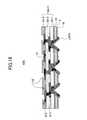
- FIG. 1is an enlarged cross-sectional view of an interposer according to a first embodiment of the present invention
- FIG. 2is a plan view of a mounting terminal viewed from a top end side
- FIG. 3Ais a plan view of a recess formed in a substrate
- FIG. 3Bis a cross-sectional view of a part of the substrate where the recess is formed;
- FIG. 4is an illustration for explaining a manufacturing process of the interposer
- FIGS. 5A through 5Iare cross-sectional views of the interposer in the steps shown in FIG. 4;
- FIG. 6Ais a cross-sectional view of an interposer having no insulating film on a back surface
- FIG. 6Bis a cross-sectional view of an interposer having an organic insulating film on a back surface
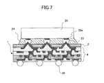
- FIG. 7is a cross-sectional view of a semiconductor package, which is formed by mounting a semiconductor device to mounting terminals of the interposer shown in FIG. 1;
- FIG. 8is a cross-sectional view of a semiconductor package in which a semiconductor device is connected to the mounting terminals of the interposer shown in FIG. 1;
- FIG. 9is a cross-sectional view of a semiconductor package, which is formed by mounting the semiconductor package of FIG. 7 onto a package substrate;
- FIG. 10is a cross-sectional view of a semiconductor package, which is formed by flip-chip mounting a semiconductor device on a side of the connection pads 14 of the interposer show in FIG. 1;
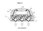
- FIG. 11is a cross-sectional view of a semiconductor package, which is formed by wire-bonding a semiconductor device to the interposer shown in FIG. 1;
- FIG. 12is a cross-sectional view of a semiconductor package, which is formed by mounting the semiconductor package shown in FIG. 10 further to a package substrate;
- FIG. 13is a cross-sectional view of the semiconductor package shown in FIG. 12 in which the mounting terminals are directly connected to the connection pads of the package substrate without using solder bumps;
- FIG. 14is an enlarged cross-sectional view of an interposer according to a second embodiment of the present invention.
- FIGS. 15A through 15Hare cross-sectional views of the interposer shown in FIG. 14 during a manufacturing process
- FIG. 16is a cross-sectional view of an interposer, which is a variation of the interposer shown in FIG. 14;
- FIG. 17is a cross-sectional view of a semiconductor package incorporating the interposer shown in FIG. 14.
- FIG. 1is an enlarged cross-sectional view of the interposer 1 according to the first embodiment of the present invention.
- the interposer 1 shown in FIG. 1comprises a silicone substrate 2 , a multilayer wiring layer 4 formed on the top surface of the silicone substrate 2 and a plurality of mounting terminals 6 projected from the undersurface of the silicone substrate 2 .
- a semiconductor elementis mounted on the upper side of the wiring layer 4 of the interposer 1 so that a semiconductor package is formed.
- the semiconductor packageis flip-chip mounted onto a circuit board via the mounting terminals 6 that protrude from the undersurface of the silicone substrate 2 .
- the mounting terminals 6are formed of a conductive layer, and the outside configuration thereof is a pyramidal shape as shown in FIG. 2. The top part of the pyramidal shape is projected from the undersurface of the silicone substrate 2 .
- Each of the mounting terminals 6has a configuration corresponding to a configuration (a reverse pyramidal shape) of a recess, which is obtained by a difference in the etching rate between the plane (111) and other planes, as shown in FIGS. 3A and 3B, by etching the silicone substrate 2 from the plane (100) side.
- a method of forming the mounting terminals 6is explained in detail later,
- the multilayer wiring layer 4 formed on the top surface side of the silicone substrate 2has a multilayer structure containing conductive layers 8 - 1 , 8 - 2 and 8 - 3 formed as wiring patterns and insulating layers 10 - 1 , 10 - 2 , 10 - 3 and 10 - 4 which insulate between conductive layers.
- the conductive layers 8 - 1 , 8 - 2 and 8 - 3 and a conductive layer 6 - 1 which extends from the root parts of the mounting terminals 6are connected by vias 12 . Thereby, connection pads 14 formed in the conductive layer 83 of the uppermost layer are electrically connected to the corresponding mounting terminals 6 .
- the multilayer wiring structure of the above-mentioned multilayer wiring layer 4is the same as a multilayer wiring structure of an existing organic fine substrate, and the detailed explanation thereof will be omitted.
- a silicone oxide film 16is formed as an insulating layer on the top surface of the silicon substrate and an inner surface of each recess in which the mounting terminal is formed.
- the silicone oxide film 18is also formed as an insulating film on the undersurface of the silicone substrate 2 . It should be noted that an organic insulating film may be formed instead of the silicone oxide film.
- the thickness of the silicone substrate 2is about 30 ⁇ m, and the thickness of the conductive layer which constitutes the mounting terminal 6 is equal to or greater than 5 ⁇ m.
- the pitch of the mounting terminals 6is about 200 ⁇ m (150 ⁇ m), and the projecting length of the end of each of the mounting terminals 6 from the back surface of the silicone substrate 2 is about 40 ⁇ m.
- FIG. 4is an illustration for explaining a manufacturing process of the interposer 1 .
- FIGS. 5A through 5Iare cross-sectional views of the interposer 1 in the steps shown in FIG. 4.
- the silicon substrate of a thickness of 650 mc having a silicon oxide film thereonis prepared, and a resist layer is formed, in step 1 , on a top surface of the silicon substrate. Then, openings corresponding to a configuration of each recess 2 a in which the mounting terminal 6 is formed by patterning the resist layer.
- the silicon substrate 2is etched using etchant such as 40% KOH solution so as to form the recesses 2 a (refer to FIG. 5A).
- the silicone substrate 2 having a surface parallel to the crystal plane (001)is used.
- step 3the resist is removed, and the silicon oxide film (SiO 2 ) is formed, in step 4 , as an insulating layer on the front surface of the silicon substrate 2 .
- the silicon oxide filmis formed by heat treatment, the silicon oxide film is formed on the entire surface of the silicon substrate 2 including the front surface, inner surfaces of the recesses 2 a and the back surface of the silicon substrate 2 .
- the formation of the silicon oxide filmmay be performed by a chemical vapor deposition (CVD) method.
- a seed metal layer of a thickness of, for example, 1 ⁇ m or lessis formed on the silicon oxide film formed on the front surface of the silicon substrate 2 and the inner surfaces of the recesses 2 a by sputtering or electroless plating (refer to FIG. 5B).
- the seed metal layeris preferably formed by sputtering of chromium (Cr) or titanium (Ti).
- step 6a resist layer is formed on the seed metal layer and the resist layer is patternized so that the mounting terminals 6 and the conductive layer 6 - 1 are formed.
- step 7a conductive layer which is made of a metal is formed on the seed metal layer.
- the conductive layeris formed of copper by Cu electrolytic plating (refer to FIG. 4C).
- the conductive layercorresponds to the mounting terminals 6 and the conductive layer 6 - 1 , and the thickness of the conductive layer is about 5 ⁇ m. Since the conductive layer is formed along the inner surface of each recess 2 a, the outside configuration of the mounting terminal 6 becomes pyramidal shape.
- step 8the resist is removed in step 8 , and the seed metal layer which exists under the removed resist is removed by etching in step 9 . Since the seed metal layer has a small thickness, light etching may be sufficient.
- step 10an insulating layer 10 - 1 is formed on the front surface side of the silicon substrate 2 , and through holes are formed at positions where the vias 12 are formed (refer to FIG. 5E).
- the insulating layer 10 - 1is formed by spin coating of polyimide or benzo-cyclobutene (BCB).
- step 11a seed metal layer is formed by sputtering on the insulating layer 10 - 1 , and a resist layer is formed and patternized on the seed metal layer in step 12 .
- step 13a conductive layer 8 - 1 which corresponds to a circuit pattern is formed by metal plating (copper electrolytic plating).
- the vias 12which connect electrically the conductive layer 8 - 1 and the conductive layer 6 - 1 are also formed simultaneously.
- the resistis removed in step 14 and the seed metal is etched in step 15 (refer to FIG. 5F).
- the multilayer wiring layer 4is formed by repeating the above-mentioned steps 10 through 15 (refer to FIG. 5G). After forming the necessary multilayer structure, nickel plating and gold plating are applied, in step 17 , to connection pads 14 formed in the uppermost layer (a conductive layer 8 - 3 in the present embodiment.).
- step 17the back surface of the silicon substrate 2 is ground using an abrasive or a grinding stone (back grinding). At this time, the grinding is proceeded slightly before the top ends of the mounting terminals 6 formed in the silicone substrate 2 .
- step 18only the silicon substrate 2 and the silicon oxide film are selectively removed by dry etching using a plasma gas so as to expose the top ends of the mounting terminals 6 (refer to FIG. 5H). In this process, the silicon oxide film (which was formed in step 4 ) adhering to the top ends of the mounting terminals 6 is also removed simultaneously. Additionally, the thickness of the silicon substrate 2 is finally set to about 30 ⁇ m.
- step 19a silicon oxide film 18 as an insulating film is formed on the back surface of the silicon substrate 2 by CVD.
- the interposer 1 shown in FIG. 1is completed by dicing the silicon substrate 2 so as to individualize the interposer 1 .
- the silicon substrate 2may be in a state where the back surface is exposed without forming the silicon oxide film 18 in step 19 .
- the reason for forming the insulating film in step 19is for avoiding a short circuit between the exposed top ends of the mounting terminals 6 and the back surface of the silicon substrate 2 .
- the silicon oxide film 16is interposed as an insulating layer between the mounting terminals 6 and the silicon substrate 2 , the insulation can be maintained at certain level even if the back surface of the silicon substrate 2 is not covered by the insulating layer.
- an organic insulating film 18 Amay be formed by a spin-coating method or the like instead of the silicone oxide film 18 .
- FIG. 7is a cross-sectional view of a semiconductor package, which is formed by mounting a semiconductor device to the mounting terminals 6 of the interposer 1 .
- Solder bumps 22are formed on electrode terminals 20 a of the semiconductor device 20 , and the solder bumps 22 are joined to the mounting terminals 6 of the interposer 1 . Since each of the mounting terminals is the top end of the pyramid and is made sharp, the mounting terminals 6 can be made protrude into the solder bumps 22 by merely pushing the solder bump 22 , thereby achieving a good electric contact. It should be noted that gold bumps may be used instead of the solder bumps. In this state, an under-fill material 24 is filled between the interposer 1 and the semiconductor device 20 so as to fix the interposer 1 to the semiconductor device 20 .
- the mounting terminals 6may be directly connected to electrode pads 20 a of the semiconductor device 20 .
- a soft metal filmis used for the metal (mounting terminals 6 ) on the electrode surface, and the interposer 1 is fixed by the under-fill material after the soft metal film is brought into contact with the electrode pads 20 . Even in this case, a good electric contact can be obtained between the mounting terminals 6 and the electrode pads 20 due to the action of the mounting terminals 6 having sharp top ends.
- FIG. 9is a cross-sectional view of the semiconductor package, which is formed by mounting the semiconductor package of FIG. 7 onto the package substrate 30 .
- the package substrate 30various substrates can be used such as a glass ceramic substrate, an alumina substrate, a build-up substrate, an FR-4 substrate and an organic substrate like a BT substrate.
- the semiconductor package containing the interposer 1is fixed to the package substrate 30 by filling an under-fill material 28 between the interposer 1 and the package substrate 30 .
- the semiconductor packagecan be formed by using the interposer 1 as a relay substrate without providing fine wirings on the package substrate even if the number of electrode pads of the semiconductor element is large and the electrode pads have fine structure.
- FIG. 10is a cross-sectional view of a semiconductor package, which is formed by flip-chip mounting the semiconductor device 20 on the side of the connection pads 14 of the interposer 1 .
- the electrode pads 20 a of the semiconductor device 20 and the connection pads 14 of the interposer 1are connected to each other by the solder ball 26 .
- the solder balls 26may be previously provided to the electrode pads 20 a of the semiconductor device 20 , or may be provided to the connection pads 14 of the interposer 1 .
- the semiconductor packageis mounted to a circuit board such as a motherboard using the mounting terminals 6 .
- FIG. 11is a cross-sectional view of the semiconductor package, which is formed by wire-bonding the semiconductor device 20 to the connection pads 14 of the interposer 1 .
- the semiconductor device 20is mounted on the multilayer wiring layer 4 of the interposer 1 in a face-up state and is fixed by a silver paste 32 or the like.
- the electrode pad 20 a of the semiconductor device 20 and the connection pads 14 of the interposer 1are electrically connected to each other by bonding wires 34 such as gold wires.
- bonding wires 34such as gold wires.
- the semiconductor device 20 and the gold wires 34are encapsulated by a bonding seal resin 36 , it can be encapsulated by transfer mold method. It should be noted that, although FIGS. 10 and 11 show the examples in which a single semiconductor element is mounted, a plurality of semiconductor elements may be mounted.
- FIG. 12is a cross-sectional view of a semiconductor package, which is formed by mounting the semiconductor package shown in FIG. 10 further to the package substrate 30 .
- the mounting terminals 6 of the interposer 1 and the connection pads 30 a of the package substrate 30are connected via solder bumps 38 .
- the solder bumps 38may be provided to the mounting terminals 6 beforehand, or provided to the connection pads 30 a of the package substrate 30 .
- gold (Au) bumpsmay be used instead of the solder bumps.
- FIG. 13is a cross-sectional view of the semiconductor package shown in FIG. 12 in which the mounting terminals 6 are directly connected to the connection pads 30 a of the package substrate 30 without using solder bumps. In this case, sufficient electrical connection can be obtained by making the top ends of the mounting terminals 6 protrude into the connection pads of the package substrate 30 .
- FIG. 14is an enlarged cross-sectional view of an interposer 40 according to the second embodiment of the present invention.
- FIGS. 15A through 15Hare cross-sectional views of the interposer 40 shown in FIG. 14 during the manufacturing process.
- parts that are the same parts shown in FIG. 1are given the same reference numerals, and descriptions thereof will be omitted.
- the interposer 40 according to the second embodiment of the present inventionhas a structure in which a multilayer wiring layer 4 A is formed on the back surface side of the silicon substrate 2 in the interposer 1 shown in FIG. 1. Therefore, the top ends of the mounting terminals 6 protrude into the multilayer wiring layer 4 A, and portions formed along the inner surfaces of the recesses 2 a of the silicon substrate 2 serve as external connection terminals.
- FIGS. 15A through 15Hthe process shown in FIGS. 15A through 15D corresponds to the process shown in FIGS. 5A through 5D.
- the conductive layeris formed only in the parts used as the mounting terminals 6 , and the conductive layer 6 - 1 is not formed.
- the back grinding and chemical etchingare performed immediately after the mounting terminals 6 are formed on the silicon substrate 2 , as shown in FIG. 15E.
- This processcan be performed in the same manner as the process shown in FIG. 5H. Thereby, The top ends of the mounting terminals are in the state where they protrude from the back surface of the silicon substrate 2 .
- the silicon oxide film 18is formed on the back surface of the silicon substrate 2 as an insulating film.
- An organic insulating filmmay be formed instead of the silicone oxide film.
- a conductive layer 42is formed on the back surface of the silicon substrate 2 by using a mask which is formed by a patternized resist on the back surface of the silicon substrate 2 .
- the conductive layer 42is formed as pattern wiring connected to the top ends of the mounting terminals 6 .
- the multilayer wiring layer 4 Ais formed on the conductive layer 42 so as to form the connection pads 14 in the uppermost part, and the interposer 40 shown in FIG. 14 is completed.
- the multilayer wiring layer 4 A shown in FIG. 14has the three-layer structure, the layer 4 A may have the four-layer structure as in the multilayer wiring layer 4 shown in FIG. 1 or may be a layered structure having an arbitrary number of layers.
- FIG. 16is a cross-sectional view of the interposer 40 A, which is a variation of the interposer shown in FIG. 14.
- the conductive layer 8 - 1 of the multilayer wiring layer 4 A- 1 and the mounting terminals 6are connected through the vias 12 without providing the conductive layer 42 .
- FIG. 17is a cross-sectional view of a semiconductor package incorporating the interposer 40 shown in FIG. 14.
- the semiconductor device 20is mounted on the package substrate 30 via the interposer 40 . That is, and electrode pads 20 a of the semiconductor device 20 are connected to the connection pads 14 of the interposer 40 by the solder bumps 22 , and the semiconductor device 20 and the interposer 40 are fixed to each other by the under-fill material 24 filled therebetween. Additionally, the mounting terminals 6 of the interposer 40 and the connection pads 30 a of the package substrate 30 are connected through the solder bumps 26 , and the interposer 40 and the package substrate 30 are fixed to each other by the under-fill material filled therebetween. Since the solder balls are accommodated inside the pyramidal shaped mounting terminals 6 , the contact area is large which gives a positive contact.
- the silicon substrateis used as a substrate of the interposer, and pyramidal shaped recesses are formed by etching so as to form the mounting terminals having the corresponding pyramidal shape.
- the present inventionis not limited to the silicon substrate, and any substrate can be used if it is easy to form a recess having a pyramidal shape including a triangular pyramid, a pentagonal pyramid or other polygonal pyramid.
- the configuration of the recessis not limited to the pyramidal shape, and a circular cone configuration where the degree of point angle is comparatively large may be used.
Landscapes
- Engineering & Computer Science (AREA)
- Microelectronics & Electronic Packaging (AREA)
- Computer Hardware Design (AREA)
- Power Engineering (AREA)
- Physics & Mathematics (AREA)
- Condensed Matter Physics & Semiconductors (AREA)
- General Physics & Mathematics (AREA)
- Manufacturing & Machinery (AREA)
- Ceramic Engineering (AREA)
- Internal Circuitry In Semiconductor Integrated Circuit Devices (AREA)
- Wire Bonding (AREA)
- Structures For Mounting Electric Components On Printed Circuit Boards (AREA)
Abstract
Description
- 1. Field of the Invention[0001]
- The present invention generally relates to semiconductor device substrates and, more particularly, to a semiconductor device substrate using a silicon substrate having fine wires formed thereon and a manufacturing method thereof.[0002]
- 2. Description of the Related Art[0003]
- With high densification of semiconductor devices, the pitch of mounting terminals of semiconductor devices has become smaller. However, since the connection-terminal pad of a circuit board on which a semiconductor device is mounted is formed with a pitch larger than the pitch of the mounting terminals of the semiconductor device, it is difficult to mount the semiconductor device as it is.[0004]
- Thus, the semiconductor device is mounted on a substrate, which is referred to as an interposer, so as to mount the semiconductor device on a circuit board via the interposer. That is, the electrodes of the semiconductor device are rearranged by the interposer so as to form mounting terminals having a larger pitch, thereby matching with the pitch of the connection-terminal pads on the circuit board.[0005]
- Generally, the above-mentioned semiconductor device substrate (interposer) has a multilayer structure in which conductive members extend from a surface on which a semiconductor device is mounted to an opposite surface on which mounting terminals are formed. Generally, an organic fine substrate is used for the interposer. In order to obtain finer wiring pattern, a silicon substrate is used in many cases. A multilayer structure is formed by stacking insulating layers and conductive layers on a silicon substrate. The conductive member that penetrates an insulating layer can be easily formed by a through hole such as a plated via hole of a build-up substrate. A silicon substrate has a relatively large thickness so as to maintain a strength as an interposer. Therefore, a special fabrication process is needed so as to form the conductive members that extend in a direction of the thickness with a fine pitch.[0006]
- An approach as one method of forming the conductive member that extends through a silicon substrate will be explained below.[0007]
- First, a thick silicon substrate is prepared, and holes having a thin cylindrical shape are formed in the silicon substrate in the same arrangement as mounting terminals. Each hole having the thin cylindrical shape is referred to as a blind via that extends to the middle of a silicon substrate. After forming an insulating film on an inner surface of each hole, a metal is filled in each hole by electro-plating or filling a metal paste. The filled metal finally becomes the conductive members that penetrate the silicon substrate, and ends thereof serve as mounting terminals to be connected to the circuit board.[0008]
- A wiring layer is formed on the top surface of the silicon substrate after filling the metal in the holes. The conductive members in the holes of the silicon substrate and the electrode pads formed on the top surface of the wiring layer are electrically connected to each other through via holes or the like. The electrodes of the semiconductor device will be connected to the electrode pads.[0009]
- After the wiring layer is formed on the top surface of the silicon substrate, ends of the conductive members in the holes of the silicon substrate are exposed by grinding (back-grinding) or etching the back surface of the silicon substrate. The back surface of the silicon substrate may be grinded until the ends of the conductive members in the holes of the silicon surface are grinded, and, thereafter, the ends of the conductive members are protruded by selectively etching only the silicon substrate. The thus-formed protruding ends serves as mounting terminals, and, thus, the semiconductor device mounted on the semiconductor device substrate (interposer) can be flip-chip mounted on the circuit board.[0010]
- With the above-mentioned fabricating method of the interposer, it is necessary to form a plurality of deep cylindrical holes in a silicon substrate that are arranged in parallel with a small pitch. In order to form such deep holes in a silicon substrate, it is necessary to use a special dry etching method such as reactive ion etching (ICP-RIE). The reactive ion etching is not used in the usual semiconductor device production process (a process for fabricating a mounting substrates such as an interposer), and needs special and expensive apparatuses and processes. Therefore, the manufacturing cost of the semiconductor device substrate (interposer) will increase.[0011]
- Moreover, the above-mentioned method needs the process for filling a metal in the deep holes in the silicon substrate. However, it is difficult to fill a metal in a deep hole without an air gap or an empty space, and a long process time is needed to fill a metal by plating.[0012]
- It is a general object of the present invention to provide an improved and useful semiconductor device substrate in which the above-mentioned problems are eliminated.[0013]
- A more specific object of the present invention is to provide a semiconductor device substrate having fine terminals with a small pitch and is able to be easily produced at a low cost without using a special process.[0014]
- In order to achieve the above-mentioned object, there is provided according to one aspect of the present invention a semiconductor device substrate comprising: a silicon substrate having a first surface and a second surface opposite to the first surface; at least one mounting terminal having a pyramidal shape and extending between the first and second surfaces, an end of the mounting terminal protruding from one of the first and second surfaces; and a wiring layer formed on the first surface of the silicon substrate, the wiring layer including a conductive layer that is electrically connected to the mounting terminal.[0015]
- According to the above-mentioned invention, the mounting terminal having a pyramidal shape can be easily formed by using the recess formed in the silicon substrate since such a recess having a pyramidal shape can be easily formed in the silicon substrate by etching which does not require special processing apparatuses. Additionally, since mounting terminal has a top of the pyramidal shape, the top end of the mounting terminal can be stuck into a member to which the mounting terminal is connected, thereby achieving a good electrical contact.[0016]
- In the semiconductor device substrate according to the present invention, an insulating film formed of a silicon oxide film may be interposed between the mounting terminal and the silicon substrate. Additionally, the first surface of the silicon substrate may be covered by an insulating layer formed of an organic insulating film. Further, the second surface of the silicon substrate may be covered by an insulating layer formed of an organic insulating film. The wiring layer may have a multiplayer structure in which insulating layers and conductive layers are alternatively stacked.[0017]
- In the semiconductor device substrate according to the present invention, the pyramidal shape of the mounting terminal may be defined by crystal planes of the silicon substrate. The first and second surfaces of the silicon substrate may be substantially parallel to the (001) plane of silicon crystal. The mounting terminal may have a hollow pyramidal shape. A top end of the mounting terminal may protrude from the second surface of the silicon substrate.[0018]
- Additionally, there is provided according to another aspect of the present invention a method of manufacturing a semiconductor device substrate, comprising the steps of: forming a recess of a pyramidal shape in a first surface of a silicon substrate; forming an insulating film on the first surface of the silicon substrate and an inner surface of the recess; forming a conductive layer in the recess, the conductive layer being configured and arranged to be a mounting terminal; forming a wiring layer on the first surface of the silicon substrate, the wiring layer including a conductive layer electrically connected to the conductive layer in the recess; and removing the silicon substrate from a second surface opposite to the first surface of the silicon substrate so as to have the conductive layer within the recess exposed in a protruding state.[0019]
- According to the above-mentioned method, the mounting terminal having a pyramidal shape can be easily formed by using the recess formed in the silicon substrate since such a recess having a pyramidal shape can be easily formed in the silicon substrate by etching which does not require special processing apparatuses. Additionally, since mounting terminal has a top of the pyramidal shape, the top end of the mounting terminal can be struck into a member to which the mounting terminal is connected, thereby achieving a good electrical contact.[0020]
- In the method according to the present invention, the step of forming the recess may include a step of removing a predetermined part of the silicon substrate in a pyramidal shape by etching. The method according to the present invention may further includes a step of forming an insulating film on a second surface of the silicon substrate opposite to the first surface after the step of removing the silicon substrate.[0021]
- The step of forming the insulating film on the second surface may include a step of forming a silicon oxide film on the second surface. Alternatively, the step of forming the insulating film on the second surface may include a step of forming an organic insulating film on the second surface. The step of removing may include: a first step of grinding the second surface of the silicon substrate; and a second step of removing the silicon substrate by etching after the first step so as to have an end of the mounting terminal protrude from the etched surface.[0022]
- Additionally, there is provided according to another aspect of the present invention a semiconductor package comprising: a semiconductor device substrate; and a semiconductor element having at least one metal bump formed on an electrode pad thereof, wherein the semiconductor device substrate comprising: a silicon substrate having a first surface and a second surface opposite to the first surface; at least one mounting terminal having a pyramidal shape and extending between the first and second surfaces, an end of the mounting terminal protruding from one of the first and second surfaces; and a wiring layer formed on the first surface of the silicon substrate, the wiring layer including a conductive layer that is electrically connected to the mounting terminal, and wherein an end of the mounting terminal of the semiconductor device substrate is connected to the metal bump in a state where the end of the mounting terminal protrudes into the metal bump. Accordingly, a good electrical connection can be achieved between the semiconductor element and the semiconductor device substrate.[0023]
- Additionally, there is provided according to another aspect of the present invention a semiconductor package comprising: a semiconductor device substrate; and a semiconductor element having at least one metal bump formed on an electrode pad thereof, wherein the semiconductor device substrate comprising: a silicon substrate having a first surface and a second surface opposite to the first surface; at least one mounting terminal having a pyramidal shape and extending between the first and second surfaces, an end of the mounting terminal protruding from one of the first and second surfaces; and a wiring layer formed on the first surface of the silicon substrate, the wiring layer including a conductive layer that is electrically connected to the mounting terminal, and wherein the semiconductor element is mounted on the wiring layer of the semiconductor device substrate, and the mounting terminal of a pyramidal shape is used as an external connection terminal. Accordingly, the external connection terminal of the semiconductor package becomes a pyramidal shape, which provides a good electrical connection when the semiconductor package is connected to a circuit board.[0024]
- Additionally, there is provided according to another aspect of the present invention a semiconductor package comprising: a semiconductor element; a semiconductor device substrate having a first surface and a second surface opposite to the first surface, the semiconductor element being mounted on the first surface; and a package substrate facing the second surface of the semiconductor device substrate and electrically connected to the semiconductor element via the semiconductor device substrate, wherein the semiconductor device substrate comprising: a silicon substrate having the first surface and the second surface opposite to the first surface; at least one mounting terminal having a pyramidal shape and extending between the first and second surfaces, an end of the mounting terminal protruding from one of the first and second surfaces; and a wiring layer formed on the first surface of the silicon substrate, the wiring layer including a conductive layer that is electrically connected to the mounting terminal. Since the semiconductor device substrate can be formed in a fine structure, the semiconductor element having a fine structure can be mounted on the package substrate without forming the package substrate in a fine structure.[0025]
- Other objects, features and advantages of the present invention will become more apparent from the following detailed description when read in conjunction with the accompanying drawings.[0026]
- FIG. 1 is an enlarged cross-sectional view of an interposer according to a first embodiment of the present invention;[0027]
- FIG. 2 is a plan view of a mounting terminal viewed from a top end side;[0028]
- FIG. 3A is a plan view of a recess formed in a substrate; FIG. 3B is a cross-sectional view of a part of the substrate where the recess is formed;[0029]
- FIG. 4 is an illustration for explaining a manufacturing process of the interposer;[0030]
- FIGS. 5A through 5I are cross-sectional views of the interposer in the steps shown in FIG. 4;[0031]
- FIG. 6A is a cross-sectional view of an interposer having no insulating film on a back surface; FIG. 6B is a cross-sectional view of an interposer having an organic insulating film on a back surface;[0032]
- FIG. 7 is a cross-sectional view of a semiconductor package, which is formed by mounting a semiconductor device to mounting terminals of the interposer shown in FIG. 1;[0033]
- FIG. 8 is a cross-sectional view of a semiconductor package in which a semiconductor device is connected to the mounting terminals of the interposer shown in FIG. 1;[0034]
- FIG. 9 is a cross-sectional view of a semiconductor package, which is formed by mounting the semiconductor package of FIG. 7 onto a package substrate;[0035]
- FIG. 10 is a cross-sectional view of a semiconductor package, which is formed by flip-chip mounting a semiconductor device on a side of the[0036]
connection pads 14 of the interposer show in FIG. 1; - FIG. 11 is a cross-sectional view of a semiconductor package, which is formed by wire-bonding a semiconductor device to the interposer shown in FIG. 1;[0037]
- FIG. 12 is a cross-sectional view of a semiconductor package, which is formed by mounting the semiconductor package shown in FIG. 10 further to a package substrate;[0038]
- FIG. 13 is a cross-sectional view of the semiconductor package shown in FIG. 12 in which the mounting terminals are directly connected to the connection pads of the package substrate without using solder bumps;[0039]
- FIG. 14 is an enlarged cross-sectional view of an interposer according to a second embodiment of the present invention;[0040]
- FIGS. 15A through 15H are cross-sectional views of the interposer shown in FIG. 14 during a manufacturing process;[0041]
- FIG. 16 is a cross-sectional view of an interposer, which is a variation of the interposer shown in FIG. 14; and[0042]
- FIG. 17 is a cross-sectional view of a semiconductor package incorporating the interposer shown in FIG. 14.[0043]
- A description will now be given, with reference to FIG. 1, of an interposer, which is a semiconductor device substrate according to a first embodiment of the present invention. FIG. 1 is an enlarged cross-sectional view of the[0044]
interposer 1 according to the first embodiment of the present invention. - The[0045]
interposer 1 shown in FIG. 1 comprises asilicone substrate 2, amultilayer wiring layer 4 formed on the top surface of thesilicone substrate 2 and a plurality of mountingterminals 6 projected from the undersurface of thesilicone substrate 2. A semiconductor element is mounted on the upper side of thewiring layer 4 of theinterposer 1 so that a semiconductor package is formed. The semiconductor package is flip-chip mounted onto a circuit board via the mountingterminals 6 that protrude from the undersurface of thesilicone substrate 2. - The mounting[0046]
terminals 6 are formed of a conductive layer, and the outside configuration thereof is a pyramidal shape as shown in FIG. 2. The top part of the pyramidal shape is projected from the undersurface of thesilicone substrate 2. Each of the mountingterminals 6 has a configuration corresponding to a configuration (a reverse pyramidal shape) of a recess, which is obtained by a difference in the etching rate between the plane (111) and other planes, as shown in FIGS. 3A and 3B, by etching thesilicone substrate 2 from the plane (100) side. A method of forming the mountingterminals 6 is explained in detail later, - The[0047]
multilayer wiring layer 4 formed on the top surface side of thesilicone substrate 2 has a multilayer structure containing conductive layers8-1,8-2 and8-3 formed as wiring patterns and insulating layers10-1,10-2,10-3 and10-4 which insulate between conductive layers. The conductive layers8-1,8-2 and8-3 and a conductive layer6-1 which extends from the root parts of the mountingterminals 6 are connected byvias 12. Thereby,connection pads 14 formed in the conductive layer83 of the uppermost layer are electrically connected to thecorresponding mounting terminals 6. - It should be noted that the multilayer wiring structure of the above-mentioned[0048]
multilayer wiring layer 4 is the same as a multilayer wiring structure of an existing organic fine substrate, and the detailed explanation thereof will be omitted. Additionally, asilicone oxide film 16 is formed as an insulating layer on the top surface of the silicon substrate and an inner surface of each recess in which the mounting terminal is formed. Thesilicone oxide film 18 is also formed as an insulating film on the undersurface of thesilicone substrate 2. It should be noted that an organic insulating film may be formed instead of the silicone oxide film. - It should be noted that, in the present embodiment, the thickness of the[0049]
silicone substrate 2 is about 30 μm, and the thickness of the conductive layer which constitutes the mountingterminal 6 is equal to or greater than 5 μm. The pitch of the mountingterminals 6 is about 200 μm (150 μm), and the projecting length of the end of each of the mountingterminals 6 from the back surface of thesilicone substrate 2 is about 40 μm. - A description will now be given, with reference to FIGS.[0050]4 and FIGS.5A through 5I, of a manufacturing method of the
interposer 1 according to the present embodiment. FIG. 4 is an illustration for explaining a manufacturing process of theinterposer 1. FIGS. 5A through 5I are cross-sectional views of theinterposer 1 in the steps shown in FIG. 4. - First, the silicon substrate of a thickness of[0051]650 mc having a silicon oxide film thereon is prepared, and a resist layer is formed, in
step 1, on a top surface of the silicon substrate. Then, openings corresponding to a configuration of eachrecess 2ain which the mountingterminal 6 is formed by patterning the resist layer. Next, instep 2, thesilicon substrate 2 is etched using etchant such as 40% KOH solution so as to form therecesses 2a(refer to FIG. 5A). In the present embodiment, thesilicone substrate 2 having a surface parallel to the crystal plane (001) is used. Therefore, when thesilicon substrate 2 is etched from a front surface side, therecesses 2ahaving a reverse pyramidal shape are formed due to the difference in the etching rate between the crystal plane (111) and other crystal planes of the silicone substrate (for example, (110):(111)=180:1). - Next, in step[0052]3, the resist is removed, and the silicon oxide film (SiO2) is formed, in
step 4, as an insulating layer on the front surface of thesilicon substrate 2. Since the silicon oxide film is formed by heat treatment, the silicon oxide film is formed on the entire surface of thesilicon substrate 2 including the front surface, inner surfaces of therecesses 2a and the back surface of thesilicon substrate 2. The formation of the silicon oxide film may be performed by a chemical vapor deposition (CVD) method. Then, in step5, a seed metal layer of a thickness of, for example, 1 μm or less is formed on the silicon oxide film formed on the front surface of thesilicon substrate 2 and the inner surfaces of therecesses 2aby sputtering or electroless plating (refer to FIG. 5B). The seed metal layer is preferably formed by sputtering of chromium (Cr) or titanium (Ti). - Next, in[0053]
step 6, a resist layer is formed on the seed metal layer and the resist layer is patternized so that the mountingterminals 6 and the conductive layer6-1 are formed. Then, instep 7, a conductive layer which is made of a metal is formed on the seed metal layer. In the present embodiment, the conductive layer is formed of copper by Cu electrolytic plating (refer to FIG. 4C). The conductive layer corresponds to the mountingterminals 6 and the conductive layer6-1, and the thickness of the conductive layer is about 5 μm. Since the conductive layer is formed along the inner surface of eachrecess 2a,the outside configuration of the mountingterminal 6 becomes pyramidal shape. - Next, the resist is removed in[0054]
step 8, and the seed metal layer which exists under the removed resist is removed by etching instep 9. Since the seed metal layer has a small thickness, light etching may be sufficient. Then, instep 10, an insulating layer10-1 is formed on the front surface side of thesilicon substrate 2, and through holes are formed at positions where thevias 12 are formed (refer to FIG. 5E). The insulating layer10-1 is formed by spin coating of polyimide or benzo-cyclobutene (BCB). - Next, in[0055]
step 11, a seed metal layer is formed by sputtering on the insulating layer10-1, and a resist layer is formed and patternized on the seed metal layer instep 12. Then, instep 13, a conductive layer8-1 which corresponds to a circuit pattern is formed by metal plating (copper electrolytic plating). At this time, thevias 12 which connect electrically the conductive layer8-1 and the conductive layer6-1 are also formed simultaneously. Then, the resist is removed instep 14 and the seed metal is etched in step15 (refer to FIG. 5F). - The[0056]
multilayer wiring layer 4 is formed by repeating the above-mentionedsteps 10 through15 (refer to FIG. 5G). After forming the necessary multilayer structure, nickel plating and gold plating are applied, instep 17, toconnection pads 14 formed in the uppermost layer (a conductive layer8-3 in the present embodiment.). - Next, in[0057]
step 17, the back surface of thesilicon substrate 2 is ground using an abrasive or a grinding stone (back grinding). At this time, the grinding is proceeded slightly before the top ends of the mountingterminals 6 formed in thesilicone substrate 2. Then, instep 18, only thesilicon substrate 2 and the silicon oxide film are selectively removed by dry etching using a plasma gas so as to expose the top ends of the mounting terminals6 (refer to FIG. 5H). In this process, the silicon oxide film (which was formed in step4) adhering to the top ends of the mountingterminals 6 is also removed simultaneously. Additionally, the thickness of thesilicon substrate 2 is finally set to about 30 μm. Then, instep 19, asilicon oxide film 18 as an insulating film is formed on the back surface of thesilicon substrate 2 by CVD. - In the above-mentioned process, in order to form a plurality of the[0058]
interposers 1 on a wafer-like silicon substrate 2 collectively, theinterposer 1 shown in FIG. 1 is completed by dicing thesilicon substrate 2 so as to individualize theinterposer 1. - Here, as shown in FIG. 6A, the[0059]
silicon substrate 2 may be in a state where the back surface is exposed without forming thesilicon oxide film 18 instep 19. The reason for forming the insulating film instep 19 is for avoiding a short circuit between the exposed top ends of the mountingterminals 6 and the back surface of thesilicon substrate 2. However, since thesilicon oxide film 16 is interposed as an insulating layer between the mountingterminals 6 and thesilicon substrate 2, the insulation can be maintained at certain level even if the back surface of thesilicon substrate 2 is not covered by the insulating layer. Moreover, as shown in FIG. 6B, an organicinsulating film 18A may be formed by a spin-coating method or the like instead of thesilicone oxide film 18. - A description will now be given of an example of forming a semiconductor package using the above-mentioned[0060]
interposer 1. - FIG. 7 is a cross-sectional view of a semiconductor package, which is formed by mounting a semiconductor device to the mounting[0061]
terminals 6 of theinterposer 1. Solder bumps22 are formed onelectrode terminals 20aof thesemiconductor device 20, and the solder bumps22 are joined to the mountingterminals 6 of theinterposer 1. Since each of the mounting terminals is the top end of the pyramid and is made sharp, the mountingterminals 6 can be made protrude into the solder bumps22 by merely pushing thesolder bump 22, thereby achieving a good electric contact. It should be noted that gold bumps may be used instead of the solder bumps. In this state, an under-fill material 24 is filled between theinterposer 1 and thesemiconductor device 20 so as to fix theinterposer 1 to thesemiconductor device 20. - Moreover, as shown in FIG. 8, the mounting[0062]
terminals 6 may be directly connected toelectrode pads 20aof thesemiconductor device 20. In this case, a soft metal film is used for the metal (mounting terminals6) on the electrode surface, and theinterposer 1 is fixed by the under-fill material after the soft metal film is brought into contact with theelectrode pads 20. Even in this case, a good electric contact can be obtained between the mountingterminals 6 and theelectrode pads 20 due to the action of the mountingterminals 6 having sharp top ends. - Furthermore, the semiconductor package shown in FIGS. 7 and 8 can be further mounted on a[0063]
package substrate 30 so as to form a semiconductor package. FIG. 9 is a cross-sectional view of the semiconductor package, which is formed by mounting the semiconductor package of FIG. 7 onto thepackage substrate 30. As for thepackage substrate 30, various substrates can be used such as a glass ceramic substrate, an alumina substrate, a build-up substrate, an FR-4 substrate and an organic substrate like a BT substrate. Moreover, after theinterposer 1 as a relay substrate is mounted on thepackage substrate 30, the semiconductor package containing theinterposer 1 is fixed to thepackage substrate 30 by filling an under-fill material 28 between theinterposer 1 and thepackage substrate 30. As shown in FIG. 9, the semiconductor package can be formed by using theinterposer 1 as a relay substrate without providing fine wirings on the package substrate even if the number of electrode pads of the semiconductor element is large and the electrode pads have fine structure. - FIG. 10 is a cross-sectional view of a semiconductor package, which is formed by flip-chip mounting the[0064]
semiconductor device 20 on the side of theconnection pads 14 of theinterposer 1. Theelectrode pads 20aof thesemiconductor device 20 and theconnection pads 14 of theinterposer 1 are connected to each other by thesolder ball 26. Thesolder balls 26 may be previously provided to theelectrode pads 20aof thesemiconductor device 20, or may be provided to theconnection pads 14 of theinterposer 1. In the case of the semiconductor package shown in FIG. 10, the semiconductor package is mounted to a circuit board such as a motherboard using the mountingterminals 6. - FIG. 11 is a cross-sectional view of the semiconductor package, which is formed by wire-bonding the[0065]
semiconductor device 20 to theconnection pads 14 of theinterposer 1. Thesemiconductor device 20 is mounted on themultilayer wiring layer 4 of theinterposer 1 in a face-up state and is fixed by asilver paste 32 or the like. Then, theelectrode pad 20aof thesemiconductor device 20 and theconnection pads 14 of theinterposer 1 are electrically connected to each other by bondingwires 34 such as gold wires. Although thesemiconductor device 20 and thegold wires 34 are encapsulated by abonding seal resin 36, it can be encapsulated by transfer mold method. It should be noted that, although FIGS. 10 and 11 show the examples in which a single semiconductor element is mounted, a plurality of semiconductor elements may be mounted. - FIG. 12 is a cross-sectional view of a semiconductor package, which is formed by mounting the semiconductor package shown in FIG. 10 further to the[0066]
package substrate 30. In the example shown in FIG. 12, the mountingterminals 6 of theinterposer 1 and theconnection pads 30aof thepackage substrate 30 are connected via solder bumps38. The solder bumps38 may be provided to the mountingterminals 6 beforehand, or provided to theconnection pads 30aof thepackage substrate 30. Moreover, gold (Au) bumps may be used instead of the solder bumps. By forming the solder bumps38 on theconnection pads 30abeforehand, sufficient electrical connection can be obtained only by pressing the mountingterminals 6 onto the solder bumps so as to protrude the ends of the mountingterminals 6 into the solder bumps. - FIG. 13 is a cross-sectional view of the semiconductor package shown in FIG. 12 in which the mounting[0067]
terminals 6 are directly connected to theconnection pads 30aof thepackage substrate 30 without using solder bumps. In this case, sufficient electrical connection can be obtained by making the top ends of the mountingterminals 6 protrude into the connection pads of thepackage substrate 30. - A description will now be given, with reference to FIG. 14 and FIGS. 15A through 15H, of a semiconductor device substrate according to the second embodiment of the present invention. FIG. 14 is an enlarged cross-sectional view of an[0068]
interposer 40 according to the second embodiment of the present invention. FIGS. 15A through 15H are cross-sectional views of theinterposer 40 shown in FIG. 14 during the manufacturing process. In FIGS. 14 and 15A through15H, parts that are the same parts shown in FIG. 1 are given the same reference numerals, and descriptions thereof will be omitted. - The[0069]
interposer 40 according to the second embodiment of the present invention has a structure in which amultilayer wiring layer 4A is formed on the back surface side of thesilicon substrate 2 in theinterposer 1 shown in FIG. 1. Therefore, the top ends of the mountingterminals 6 protrude into themultilayer wiring layer 4A, and portions formed along the inner surfaces of therecesses 2aof thesilicon substrate 2 serve as external connection terminals. - In the manufacturing process shown in FIGS. 15A through 15H, the process shown in FIGS. 15A through 15D corresponds to the process shown in FIGS. 5A through 5D. However, in FIG. 15C, the conductive layer is formed only in the parts used as the mounting[0070]
terminals 6, and the conductive layer6-1 is not formed. - In the present embodiment, the back grinding and chemical etching are performed immediately after the mounting[0071]
terminals 6 are formed on thesilicon substrate 2, as shown in FIG. 15E. This process can be performed in the same manner as the process shown in FIG. 5H. Thereby, The top ends of the mounting terminals are in the state where they protrude from the back surface of thesilicon substrate 2. Next, as shown in FIG. 15F, thesilicon oxide film 18 is formed on the back surface of thesilicon substrate 2 as an insulating film. An organic insulating film may be formed instead of the silicone oxide film. - Then, as shown in FIG. 15G, a[0072]
conductive layer 42 is formed on the back surface of thesilicon substrate 2 by using a mask which is formed by a patternized resist on the back surface of thesilicon substrate 2. Theconductive layer 42 is formed as pattern wiring connected to the top ends of the mountingterminals 6. Then, as shown in FIG. 15H, themultilayer wiring layer 4A is formed on theconductive layer 42 so as to form theconnection pads 14 in the uppermost part, and theinterposer 40 shown in FIG. 14 is completed. It to should be noted that although themultilayer wiring layer 4A shown in FIG. 14 has the three-layer structure, thelayer 4A may have the four-layer structure as in themultilayer wiring layer 4 shown in FIG. 1 or may be a layered structure having an arbitrary number of layers. - FIG. 16 is a cross-sectional view of the[0073]
interposer 40A, which is a variation of the interposer shown in FIG. 14. In theinterposer 40A, the conductive layer8-1 of themultilayer wiring layer 4A-1 and the mountingterminals 6 are connected through thevias 12 without providing theconductive layer 42. - FIG. 17 is a cross-sectional view of a semiconductor package incorporating the[0074]
interposer 40 shown in FIG. 14. Thesemiconductor device 20 is mounted on thepackage substrate 30 via theinterposer 40. That is, andelectrode pads 20aof thesemiconductor device 20 are connected to theconnection pads 14 of theinterposer 40 by the solder bumps22, and thesemiconductor device 20 and theinterposer 40 are fixed to each other by the under-fill material 24 filled therebetween. Additionally, the mountingterminals 6 of theinterposer 40 and theconnection pads 30aof thepackage substrate 30 are connected through the solder bumps26, and theinterposer 40 and thepackage substrate 30 are fixed to each other by the under-fill material filled therebetween. Since the solder balls are accommodated inside the pyramidal shaped mountingterminals 6, the contact area is large which gives a positive contact. - In the above-mentioned embodiments, the silicon substrate is used as a substrate of the interposer, and pyramidal shaped recesses are formed by etching so as to form the mounting terminals having the corresponding pyramidal shape. The present invention is not limited to the silicon substrate, and any substrate can be used if it is easy to form a recess having a pyramidal shape including a triangular pyramid, a pentagonal pyramid or other polygonal pyramid. Moreover, the configuration of the recess is not limited to the pyramidal shape, and a circular cone configuration where the degree of point angle is comparatively large may be used.[0075]
- The present invention is not limited to the specifically disclosed embodiments, and variations and modifications may be made without departing from the scope of the present invention.[0076]
Claims (18)
Priority Applications (1)
| Application Number | Priority Date | Filing Date | Title |
|---|---|---|---|
| US10/862,403US6905951B2 (en) | 2002-02-22 | 2004-06-08 | Method of forming a device substrate and semiconductor package including a pyramid contact |
Applications Claiming Priority (2)
| Application Number | Priority Date | Filing Date | Title |
|---|---|---|---|
| JP2002046448AJP4044769B2 (en) | 2002-02-22 | 2002-02-22 | Semiconductor device substrate, manufacturing method thereof, and semiconductor package |
| JP2002-046448 | 2002-02-22 |
Related Child Applications (1)
| Application Number | Title | Priority Date | Filing Date |
|---|---|---|---|
| US10/862,403DivisionUS6905951B2 (en) | 2002-02-22 | 2004-06-08 | Method of forming a device substrate and semiconductor package including a pyramid contact |
Publications (2)
| Publication Number | Publication Date |
|---|---|
| US20030160325A1true US20030160325A1 (en) | 2003-08-28 |
| US6781224B2 US6781224B2 (en) | 2004-08-24 |
Family
ID=27750633
Family Applications (2)
| Application Number | Title | Priority Date | Filing Date |
|---|---|---|---|
| US10/262,074Expired - LifetimeUS6781224B2 (en) | 2002-02-22 | 2002-10-02 | Semiconductor device and package including forming pyramid mount protruding through silicon substrate |
| US10/862,403Expired - Fee RelatedUS6905951B2 (en) | 2002-02-22 | 2004-06-08 | Method of forming a device substrate and semiconductor package including a pyramid contact |
Family Applications After (1)
| Application Number | Title | Priority Date | Filing Date |
|---|---|---|---|
| US10/862,403Expired - Fee RelatedUS6905951B2 (en) | 2002-02-22 | 2004-06-08 | Method of forming a device substrate and semiconductor package including a pyramid contact |
Country Status (5)
| Country | Link |
|---|---|
| US (2) | US6781224B2 (en) |
| JP (1) | JP4044769B2 (en) |
| KR (1) | KR100847033B1 (en) |
| CN (1) | CN1225783C (en) |
| TW (1) | TW563231B (en) |
Cited By (38)
| Publication number | Priority date | Publication date | Assignee | Title |
|---|---|---|---|---|
| US20030152691A1 (en)* | 2002-02-14 | 2003-08-14 | 3M Innovative Properties Company | In-line deposition processes for circuit fabrication |
| US20030150384A1 (en)* | 2002-02-14 | 2003-08-14 | 3M Innovative Properties Company | Aperture masks for circuit fabrication |
| US20040238952A1 (en)* | 2002-07-11 | 2004-12-02 | Farnworth Warren M. | Asymmetric plating |
| US20050006763A1 (en)* | 2003-06-02 | 2005-01-13 | Seiko Epson Corporation | Circuit substrate, semiconductor module and method of manufacturing circuit substrate |
| US20050263911A1 (en)* | 2004-05-31 | 2005-12-01 | Yusuke Igarashi | Circuit device and manufacturing method thereof |
| US20060001166A1 (en)* | 2004-06-30 | 2006-01-05 | Yusuke Igarashi | Circuit device and manufacturing method thereof |
| US20060012048A1 (en)* | 2004-07-07 | 2006-01-19 | Nec Corporation And Nec Electronics Corporation | Wiring substrate for mounting semiconductors, method of manufacturing the same, and semiconductor package |
| US20060121719A1 (en)* | 2004-12-01 | 2006-06-08 | Shinko Electric Industries Co., Ltd. | Method of manufacturing a circuit substrate and method of manufacturing an electronic parts packaging structure |
| US20060131730A1 (en)* | 2004-12-16 | 2006-06-22 | Junichi Nakamura | Semiconductor package and fabrication method |
| US20070069364A1 (en)* | 2005-09-29 | 2007-03-29 | Nec Electronics Corporation | Semiconductor device and method for manufacturing same |
| US20070102816A1 (en)* | 2005-11-08 | 2007-05-10 | Samsung Electronics Co., Ltd. | Board structure, a ball grid array (BGA) package and method thereof, and a solder ball and method thereof |
| WO2007008171A3 (en)* | 2005-07-09 | 2007-06-07 | Gautham Viswanadam | Integrated circuit device and method of manufacturing thereof |
| US20070145518A1 (en)* | 2005-12-28 | 2007-06-28 | Casio Computer Co., Ltd. | Circuit board, semiconductor device, and manufacturing method of circuit board |
| US20070170578A1 (en)* | 2006-01-26 | 2007-07-26 | Noriyuki Yoshikawa | Semiconductor device, electronic apparatus comprising the same, and method for fabrication of substrate for semiconductor device used therein |
| US20090140442A1 (en)* | 2007-12-03 | 2009-06-04 | Stats Chippac, Ltd. | Wafer Level Package Integration and Method |
| US20090227073A1 (en)* | 2008-03-07 | 2009-09-10 | Ki Yong Lee | Method for manufacturing semiconductor package having improved bump structures |
| US20090309218A1 (en)* | 2008-06-17 | 2009-12-17 | Renesas Technology Corp. | Semiconductor device and method of manufacturing the same |
| US20100288550A1 (en)* | 2007-09-28 | 2010-11-18 | Masayuki Nagamatsu | ELEMENT MOUNTING SUBSTRATE AND METHOD OF FABRICATING THE SAME, CIRCUIT DEVICE AND METHOD OF FABRICATING THE SAME, AND MOBILE APPLIANCE ( as amended |
| US20110175218A1 (en)* | 2010-01-18 | 2011-07-21 | Shiann-Ming Liou | Package assembly having a semiconductor substrate |
| US20110186998A1 (en)* | 2010-02-03 | 2011-08-04 | Albert Wu | Recessed semiconductor substrates |
| US20130009293A1 (en)* | 2011-07-08 | 2013-01-10 | Unimicron Technology Corporation | Packaging substrate and method of fabricating the same |
| US20130026609A1 (en)* | 2010-01-18 | 2013-01-31 | Marvell World Trade Ltd. | Package assembly including a semiconductor substrate with stress relief structure |
| US20140306355A1 (en)* | 2013-04-15 | 2014-10-16 | Thorsten Meyer | Chip interposer, semiconductor device, and method for manufacturing a semiconductor device |
| US20150008577A1 (en)* | 2007-12-18 | 2015-01-08 | Micron Technology, Inc. | Methods of fluxless micro-piercing of solder balls, and resulting devices |
| US20150311155A1 (en)* | 2003-12-17 | 2015-10-29 | Seiko Epson Corporation | Semiconductor device, method of manufacturing thereof, circuit board and electronic apparatus |
| US9198290B2 (en) | 2011-09-15 | 2015-11-24 | Shinko Electric Industries Co., Ltd. | Wiring substrate, method of manufacturing the same, and semiconductor device |
| US9326372B2 (en)* | 2013-03-18 | 2016-04-26 | Fujitsu Limited | Semiconductor device manufacturing method and semiconductor mounting substrate |
| US9460951B2 (en) | 2007-12-03 | 2016-10-04 | STATS ChipPAC Pte. Ltd. | Semiconductor device and method of wafer level package integration |
| US9748167B1 (en)* | 2016-07-25 | 2017-08-29 | United Microelectronics Corp. | Silicon interposer, semiconductor package using the same, and fabrication method thereof |
| US9859202B2 (en)* | 2015-06-24 | 2018-01-02 | Dyi-chung Hu | Spacer connector |
| WO2021034624A1 (en)* | 2019-08-21 | 2021-02-25 | Facebook Technologies, Llc | Atomic force microscopy tips for interconnection |
| US11037874B2 (en)* | 2018-10-29 | 2021-06-15 | Intel Corporation | Plane-less voltage reference interconnects |
| US11064609B2 (en)* | 2016-08-04 | 2021-07-13 | X Display Company Technology Limited | Printable 3D electronic structure |
| US11387178B2 (en)* | 2020-03-06 | 2022-07-12 | X-Celeprint Limited | Printable 3D electronic components and structures |
| US20220246472A1 (en)* | 2019-07-22 | 2022-08-04 | International Business Machines Corporation | Dual redistribution layer structure |
| US20220293509A1 (en)* | 2021-03-10 | 2022-09-15 | Intel Corporation | Dielectric-to-metal adhesion promotion material |
| US11640934B2 (en)* | 2018-03-30 | 2023-05-02 | Intel Corporation | Lithographically defined vertical interconnect access (VIA) in dielectric pockets in a package substrate |
| US12205877B2 (en)* | 2019-02-21 | 2025-01-21 | AT&S(Chongqing) Company Limited | Ultra-thin component carrier having high stiffness and method of manufacturing the same |
Families Citing this family (21)
| Publication number | Priority date | Publication date | Assignee | Title |
|---|---|---|---|---|
| KR100499006B1 (en)* | 2002-12-30 | 2005-07-01 | 삼성전기주식회사 | Manufacturing method for package substrate without electrolytic plating lead |
| JP4865197B2 (en)* | 2004-06-30 | 2012-02-01 | ルネサスエレクトロニクス株式会社 | Semiconductor device and manufacturing method thereof |
| JP5653144B2 (en)* | 2004-12-16 | 2015-01-14 | 新光電気工業株式会社 | Manufacturing method of semiconductor package |
| US8048789B2 (en)* | 2005-04-26 | 2011-11-01 | Northwestern University | Mesoscale pyramids, arrays and methods of preparation |
| JP4503039B2 (en)* | 2006-04-27 | 2010-07-14 | 三洋電機株式会社 | Circuit equipment |
| KR100824635B1 (en)* | 2006-09-13 | 2008-04-24 | 동부일렉트로닉스 주식회사 | Inductor manufacturing method using system-in-package |
| JP2009123763A (en)* | 2007-11-12 | 2009-06-04 | Denso Corp | Semiconductor device and manufacturing method thereof |
| KR20100037300A (en)* | 2008-10-01 | 2010-04-09 | 삼성전자주식회사 | Method of forming semiconductor device having embedded interposer |
| US7964974B2 (en)* | 2008-12-02 | 2011-06-21 | General Electric Company | Electronic chip package with reduced contact pad pitch |
| JP2010157690A (en) | 2008-12-29 | 2010-07-15 | Ibiden Co Ltd | Board for mounting electronic component thereon, and method of manufacturing the same |
| US8344495B2 (en)* | 2009-12-11 | 2013-01-01 | Stats Chippac Ltd. | Integrated circuit packaging system with interconnect and method of manufacture thereof |
| JP5377403B2 (en)* | 2010-04-28 | 2013-12-25 | 株式会社テラミクロス | Semiconductor device and circuit board manufacturing method |
| US8802504B1 (en)* | 2013-03-14 | 2014-08-12 | Taiwan Semiconductor Manufacturing Company, Ltd. | 3D packages and methods for forming the same |
| US9299649B2 (en) | 2013-02-08 | 2016-03-29 | Taiwan Semiconductor Manufacturing Company, Ltd. | 3D packages and methods for forming the same |
| JP6623508B2 (en) | 2014-09-30 | 2019-12-25 | 日亜化学工業株式会社 | Light source, method of manufacturing and mounting method |
| TWI557819B (en)* | 2014-12-04 | 2016-11-11 | 欣興電子股份有限公司 | Interposer and manufacturing method thereof |
| US10468363B2 (en)* | 2015-08-10 | 2019-11-05 | X-Celeprint Limited | Chiplets with connection posts |
| US11495560B2 (en)* | 2015-08-10 | 2022-11-08 | X Display Company Technology Limited | Chiplets with connection posts |
| KR102019355B1 (en)* | 2017-11-01 | 2019-09-09 | 삼성전자주식회사 | Semiconductor package |
| JP7087369B2 (en)* | 2017-12-13 | 2022-06-21 | 凸版印刷株式会社 | Manufacturing method of carrier substrate with fine wiring layer and semiconductor package substrate with fine wiring layer |
| US20240071890A1 (en)* | 2022-08-30 | 2024-02-29 | Taiwan Semiconductor Manufacturing Company Limited | Semiconductor package including a surface with a plurality of roughness values and methods of forming the same |
Citations (4)
| Publication number | Priority date | Publication date | Assignee | Title |
|---|---|---|---|---|
| US6114221A (en)* | 1998-03-16 | 2000-09-05 | International Business Machines Corporation | Method and apparatus for interconnecting multiple circuit chips |
| US20020030245A1 (en)* | 2000-06-02 | 2002-03-14 | Seiko Epson Corporation | Semiconductor device, method of fabricating the same, stack-type semiconductor device, circuit board and electronic instrument |
| US20020115293A1 (en)* | 2001-01-03 | 2002-08-22 | Bahram Ghodsian | Device to rapidly and accurately sequence long DNA fragments |
| US6548315B2 (en)* | 1999-09-27 | 2003-04-15 | Hitachi, Ltd. | Manufacture method for semiconductor inspection apparatus |
Family Cites Families (4)
| Publication number | Priority date | Publication date | Assignee | Title |
|---|---|---|---|---|
| US30245A (en)* | 1860-10-02 | Improvement in revolving fire-arms | ||
| JP3186941B2 (en)* | 1995-02-07 | 2001-07-11 | シャープ株式会社 | Semiconductor chips and multi-chip semiconductor modules |
| JP3903650B2 (en)* | 1999-06-18 | 2007-04-11 | 住友電気工業株式会社 | Optical amplifier and optical amplifier control method |
| JP4043146B2 (en) | 1999-06-25 | 2008-02-06 | イビデン株式会社 | Package substrate |
- 2002
- 2002-02-22JPJP2002046448Apatent/JP4044769B2/ennot_activeExpired - Fee Related
- 2002-10-02USUS10/262,074patent/US6781224B2/ennot_activeExpired - Lifetime
- 2002-10-03TWTW091122868Apatent/TW563231B/ennot_activeIP Right Cessation
- 2002-10-15KRKR1020020062626Apatent/KR100847033B1/ennot_activeExpired - Fee Related
- 2002-10-25CNCNB021471800Apatent/CN1225783C/ennot_activeExpired - Fee Related
- 2004
- 2004-06-08USUS10/862,403patent/US6905951B2/ennot_activeExpired - Fee Related
Patent Citations (4)
| Publication number | Priority date | Publication date | Assignee | Title |
|---|---|---|---|---|
| US6114221A (en)* | 1998-03-16 | 2000-09-05 | International Business Machines Corporation | Method and apparatus for interconnecting multiple circuit chips |
| US6548315B2 (en)* | 1999-09-27 | 2003-04-15 | Hitachi, Ltd. | Manufacture method for semiconductor inspection apparatus |
| US20020030245A1 (en)* | 2000-06-02 | 2002-03-14 | Seiko Epson Corporation | Semiconductor device, method of fabricating the same, stack-type semiconductor device, circuit board and electronic instrument |
| US20020115293A1 (en)* | 2001-01-03 | 2002-08-22 | Bahram Ghodsian | Device to rapidly and accurately sequence long DNA fragments |
Cited By (84)
| Publication number | Priority date | Publication date | Assignee | Title |
|---|---|---|---|---|
| US20030152691A1 (en)* | 2002-02-14 | 2003-08-14 | 3M Innovative Properties Company | In-line deposition processes for circuit fabrication |
| US20030150384A1 (en)* | 2002-02-14 | 2003-08-14 | 3M Innovative Properties Company | Aperture masks for circuit fabrication |
| US6821348B2 (en)* | 2002-02-14 | 2004-11-23 | 3M Innovative Properties Company | In-line deposition processes for circuit fabrication |
| US7241688B2 (en) | 2002-02-14 | 2007-07-10 | 3M Innovative Properties Company | Aperture masks for circuit fabrication |
| US6897164B2 (en)* | 2002-02-14 | 2005-05-24 | 3M Innovative Properties Company | Aperture masks for circuit fabrication |
| US20050191572A1 (en)* | 2002-02-14 | 2005-09-01 | 3M Innovative Properties Company | Aperture masks for circuit fabrication |
| US20080038935A1 (en)* | 2002-02-14 | 2008-02-14 | 3M Innovative Properties Company | Aperture masks for circuit fabrication |
| US20040238952A1 (en)* | 2002-07-11 | 2004-12-02 | Farnworth Warren M. | Asymmetric plating |
| US7190065B2 (en)* | 2003-06-02 | 2007-03-13 | Seiko Epson Corporation | Circuit substrate, semiconductor module and method of manufacturing circuit substrate |
| US20050006763A1 (en)* | 2003-06-02 | 2005-01-13 | Seiko Epson Corporation | Circuit substrate, semiconductor module and method of manufacturing circuit substrate |
| US20150311155A1 (en)* | 2003-12-17 | 2015-10-29 | Seiko Epson Corporation | Semiconductor device, method of manufacturing thereof, circuit board and electronic apparatus |
| US9589886B2 (en)* | 2003-12-17 | 2017-03-07 | Seiko Epson Corporation | Semiconductor device, method of manufacturing thereof, circuit board and electronic apparatus |
| US7315083B2 (en)* | 2004-05-31 | 2008-01-01 | Sanyo Electric Co., Ltd. | Circuit device and manufacturing method thereof |
| US20050263911A1 (en)* | 2004-05-31 | 2005-12-01 | Yusuke Igarashi | Circuit device and manufacturing method thereof |
| US7768132B2 (en)* | 2004-06-30 | 2010-08-03 | Sanyo Electric Co., Ltd. | Circuit device and manufacturing method thereof |
| US20060001166A1 (en)* | 2004-06-30 | 2006-01-05 | Yusuke Igarashi | Circuit device and manufacturing method thereof |
| US20060012048A1 (en)* | 2004-07-07 | 2006-01-19 | Nec Corporation And Nec Electronics Corporation | Wiring substrate for mounting semiconductors, method of manufacturing the same, and semiconductor package |
| US7816782B2 (en)* | 2004-07-07 | 2010-10-19 | Nec Corporation | Wiring substrate for mounting semiconductors, method of manufacturing the same, and semiconductor package |
| US20060121719A1 (en)* | 2004-12-01 | 2006-06-08 | Shinko Electric Industries Co., Ltd. | Method of manufacturing a circuit substrate and method of manufacturing an electronic parts packaging structure |
| TWI395274B (en)* | 2004-12-01 | 2013-05-01 | Shinko Electric Ind Co | Method of manufacturing a circuit substrate and method of manufacturing an electronic parts packaging structure |
| US7435680B2 (en)* | 2004-12-01 | 2008-10-14 | Shinko Electric Industries Co., Ltd. | Method of manufacturing a circuit substrate and method of manufacturing an electronic parts packaging structure |
| CN1832152B (en)* | 2004-12-16 | 2010-05-26 | 新光电气工业株式会社 | Semiconductor packaging and manufacturing method |
| TWI471956B (en)* | 2004-12-16 | 2015-02-01 | Shinko Electric Ind Co | Semiconductor package and manufacturing method |
| US7838982B2 (en)* | 2004-12-16 | 2010-11-23 | Shinko Electric Industries Co., Ltd. | Semiconductor package having connecting bumps |
| US20060131730A1 (en)* | 2004-12-16 | 2006-06-22 | Junichi Nakamura | Semiconductor package and fabrication method |
| US20100144093A1 (en)* | 2005-07-09 | 2010-06-10 | Gautham Viswanadam | Integrated Circuit Device and Method of Manufacturing Thereof |
| US7785928B2 (en) | 2005-07-09 | 2010-08-31 | Gautham Viswanadam | Integrated circuit device and method of manufacturing thereof |
| WO2007008171A3 (en)* | 2005-07-09 | 2007-06-07 | Gautham Viswanadam | Integrated circuit device and method of manufacturing thereof |
| US8183685B2 (en) | 2005-09-29 | 2012-05-22 | Renesas Electronics Corporation | Semiconductor device |
| US20070069364A1 (en)* | 2005-09-29 | 2007-03-29 | Nec Electronics Corporation | Semiconductor device and method for manufacturing same |
| US20100048019A1 (en)* | 2005-09-29 | 2010-02-25 | Nec Electronics Corporation | Method for manufacturing a semiconductor device |
| US8456019B2 (en) | 2005-09-29 | 2013-06-04 | Renesas Electronics Corporation | Semiconductor device |
| US7633167B2 (en)* | 2005-09-29 | 2009-12-15 | Nec Electronics Corporation | Semiconductor device and method for manufacturing same |
| US20110101541A1 (en)* | 2005-09-29 | 2011-05-05 | Renesas Electronics Corporation | Semiconductor device |
| US7892973B2 (en) | 2005-09-29 | 2011-02-22 | Renesas Electronics Corporation | Method for manufacturing a semiconductor device |
| US20070102816A1 (en)* | 2005-11-08 | 2007-05-10 | Samsung Electronics Co., Ltd. | Board structure, a ball grid array (BGA) package and method thereof, and a solder ball and method thereof |
| US7791195B2 (en)* | 2005-11-08 | 2010-09-07 | Samsung Electronics Co., Ltd. | Ball grid array (BGA) package and method thereof |
| US20090174062A1 (en)* | 2005-12-28 | 2009-07-09 | Casio Computer Co., Ltd. | Circuit board, semiconductor device, and manufacturing method of circuit board |
| US7528480B2 (en)* | 2005-12-28 | 2009-05-05 | Casio Computer Co., Ltd. | Circuit board, semiconductor device, and manufacturing method of circuit board |
| US20070145518A1 (en)* | 2005-12-28 | 2007-06-28 | Casio Computer Co., Ltd. | Circuit board, semiconductor device, and manufacturing method of circuit board |
| US20070170578A1 (en)* | 2006-01-26 | 2007-07-26 | Noriyuki Yoshikawa | Semiconductor device, electronic apparatus comprising the same, and method for fabrication of substrate for semiconductor device used therein |
| US7719119B2 (en)* | 2006-01-26 | 2010-05-18 | Panasonic Corporation | Semiconductor device, electronic apparatus comprising the same, and method for fabrication of substrate for semiconductor device used therein |
| US20100288550A1 (en)* | 2007-09-28 | 2010-11-18 | Masayuki Nagamatsu | ELEMENT MOUNTING SUBSTRATE AND METHOD OF FABRICATING THE SAME, CIRCUIT DEVICE AND METHOD OF FABRICATING THE SAME, AND MOBILE APPLIANCE ( as amended |
| US9460951B2 (en) | 2007-12-03 | 2016-10-04 | STATS ChipPAC Pte. Ltd. | Semiconductor device and method of wafer level package integration |
| US10074553B2 (en)* | 2007-12-03 | 2018-09-11 | STATS ChipPAC Pte. Ltd. | Wafer level package integration and method |
| US20090140442A1 (en)* | 2007-12-03 | 2009-06-04 | Stats Chippac, Ltd. | Wafer Level Package Integration and Method |
| US20150008577A1 (en)* | 2007-12-18 | 2015-01-08 | Micron Technology, Inc. | Methods of fluxless micro-piercing of solder balls, and resulting devices |
| US10163840B2 (en)* | 2007-12-18 | 2018-12-25 | Micron Technology, Inc. | Methods of fluxless micro-piercing of solder balls, and resulting devices |
| US10515918B2 (en) | 2007-12-18 | 2019-12-24 | Micron Technology, Inc. | Methods of fluxless micro-piercing of solder balls, and resulting devices |
| US8383461B2 (en)* | 2008-03-07 | 2013-02-26 | Hynix Semiconductor Inc. | Method for manufacturing semiconductor package having improved bump structures |
| US20090227073A1 (en)* | 2008-03-07 | 2009-09-10 | Ki Yong Lee | Method for manufacturing semiconductor package having improved bump structures |
| US20090309218A1 (en)* | 2008-06-17 | 2009-12-17 | Renesas Technology Corp. | Semiconductor device and method of manufacturing the same |
| US8178977B2 (en)* | 2008-06-17 | 2012-05-15 | Renesas Electronics Corporation | Semiconductor device and method of manufacturing the same |
| US9275929B2 (en) | 2010-01-18 | 2016-03-01 | Marvell World Trade Ltd. | Package assembly having a semiconductor substrate |
| US20130026609A1 (en)* | 2010-01-18 | 2013-01-31 | Marvell World Trade Ltd. | Package assembly including a semiconductor substrate with stress relief structure |
| US20110175218A1 (en)* | 2010-01-18 | 2011-07-21 | Shiann-Ming Liou | Package assembly having a semiconductor substrate |
| US9768144B2 (en) | 2010-02-03 | 2017-09-19 | Marvell World Trade Ltd. | Package assembly including a semiconductor substrate in which a first portion of a surface of the semiconductor substrate is recessed relative to a second portion of the surface of the semiconductor substrate to form a recessed region in the semiconductor substrate |
| US20110186998A1 (en)* | 2010-02-03 | 2011-08-04 | Albert Wu | Recessed semiconductor substrates |
| US9257410B2 (en) | 2010-02-03 | 2016-02-09 | Marvell World Trade Ltd. | Package assembly including a semiconductor substrate in which a first portion of a surface of the semiconductor substrate is recessed relative to a second portion of the surface of the semiconductor substrate to form a recessed region in the semiconductor substrate |
| US8624382B2 (en)* | 2011-07-08 | 2014-01-07 | Unimicron Technology Corporation | Packaging substrate and method of fabricating the same |
| US20130009293A1 (en)* | 2011-07-08 | 2013-01-10 | Unimicron Technology Corporation | Packaging substrate and method of fabricating the same |
| US9070616B2 (en)* | 2011-07-08 | 2015-06-30 | Unimicron Technology Corporation | Method of fabricating packaging substrate |
| US20140090794A1 (en)* | 2011-07-08 | 2014-04-03 | Unimicron Technology Corporation | Method of fabricating packaging substrate |
| US9198290B2 (en) | 2011-09-15 | 2015-11-24 | Shinko Electric Industries Co., Ltd. | Wiring substrate, method of manufacturing the same, and semiconductor device |
| WO2013072775A3 (en)* | 2011-10-10 | 2013-11-21 | Marvell World Trade Ltd. | Package assembly including a semiconductor substrate with stress relief structure |
| US9326372B2 (en)* | 2013-03-18 | 2016-04-26 | Fujitsu Limited | Semiconductor device manufacturing method and semiconductor mounting substrate |
| US9263376B2 (en)* | 2013-04-15 | 2016-02-16 | Intel Deutschland Gmbh | Chip interposer, semiconductor device, and method for manufacturing a semiconductor device |
| US20140306355A1 (en)* | 2013-04-15 | 2014-10-16 | Thorsten Meyer | Chip interposer, semiconductor device, and method for manufacturing a semiconductor device |
| US9859202B2 (en)* | 2015-06-24 | 2018-01-02 | Dyi-chung Hu | Spacer connector |
| US9748167B1 (en)* | 2016-07-25 | 2017-08-29 | United Microelectronics Corp. | Silicon interposer, semiconductor package using the same, and fabrication method thereof |
| US11064609B2 (en)* | 2016-08-04 | 2021-07-13 | X Display Company Technology Limited | Printable 3D electronic structure |
| US11640934B2 (en)* | 2018-03-30 | 2023-05-02 | Intel Corporation | Lithographically defined vertical interconnect access (VIA) in dielectric pockets in a package substrate |
| US11037874B2 (en)* | 2018-10-29 | 2021-06-15 | Intel Corporation | Plane-less voltage reference interconnects |
| US12205877B2 (en)* | 2019-02-21 | 2025-01-21 | AT&S(Chongqing) Company Limited | Ultra-thin component carrier having high stiffness and method of manufacturing the same |
| US20220246472A1 (en)* | 2019-07-22 | 2022-08-04 | International Business Machines Corporation | Dual redistribution layer structure |
| US12438046B2 (en)* | 2019-07-22 | 2025-10-07 | International Business Machines Corporation | Dual redistribution layer structure |
| US10989735B2 (en) | 2019-08-21 | 2021-04-27 | Facebook Technologies, Llc | Atomic force microscopy tips for interconnection |
| CN114174839A (en)* | 2019-08-21 | 2022-03-11 | 脸谱科技有限责任公司 | Atomic Force Microscope Tips for Interconnects |
| US11296268B1 (en) | 2019-08-21 | 2022-04-05 | Facebook Technologies, Llc | Magnetic clamping interconnects |
| WO2021034624A1 (en)* | 2019-08-21 | 2021-02-25 | Facebook Technologies, Llc | Atomic force microscopy tips for interconnection |
| US11417792B1 (en) | 2019-08-21 | 2022-08-16 | Meta Platforms Technologies, Llc | Interconnect with nanotube fitting |
| US11387178B2 (en)* | 2020-03-06 | 2022-07-12 | X-Celeprint Limited | Printable 3D electronic components and structures |
| US12159825B2 (en)* | 2021-03-10 | 2024-12-03 | Intel Corporation | Dielectric-to-metal adhesion promotion material |
| US20220293509A1 (en)* | 2021-03-10 | 2022-09-15 | Intel Corporation | Dielectric-to-metal adhesion promotion material |
Also Published As
| Publication number | Publication date |
|---|---|
| JP2003249601A (en) | 2003-09-05 |
| CN1440073A (en) | 2003-09-03 |
| TW563231B (en) | 2003-11-21 |
| KR100847033B1 (en) | 2008-07-17 |
| JP4044769B2 (en) | 2008-02-06 |
| CN1225783C (en) | 2005-11-02 |
| US6905951B2 (en) | 2005-06-14 |
| US20040224499A1 (en) | 2004-11-11 |
| US6781224B2 (en) | 2004-08-24 |
| KR20030069774A (en) | 2003-08-27 |
Similar Documents
| Publication | Publication Date | Title |
|---|---|---|
| US6781224B2 (en) | Semiconductor device and package including forming pyramid mount protruding through silicon substrate | |
| US10297582B2 (en) | BVA interposer | |
| US9412677B2 (en) | Computer systems having an interposer including a flexible material | |
| US6611052B2 (en) | Wafer level stackable semiconductor package | |
| EP2172089B1 (en) | Method for manufacturing a multilayer wiring element having pin interface | |
| US7763965B2 (en) | Stress relief structures for silicon interposers | |
| US8178957B2 (en) | Electronic component device, and method of manufacturing the same | |
| JP2007110117A (en) | Wafer level chip scale package of image sensor and manufacturing method thereof | |
| JP5942823B2 (en) | Electronic component device manufacturing method, electronic component device, and electronic device | |
| US20050019982A1 (en) | Semiconductor package having semiconductor constructing body and method of manufacturing the same | |
| US20110092065A1 (en) | Semiconductor device suitable for a stacked structure | |
| TW202133282A (en) | Semiconductor package | |
| US20100294552A1 (en) | Electronic component mounted structure | |
| US6236112B1 (en) | Semiconductor device, connecting substrate therefor, and process of manufacturing connecting substrate | |
| KR20130086347A (en) | Stackable molded microelectronic packages with area array unit connectors | |
| US7074704B2 (en) | Bump formed on semiconductor device chip and method for manufacturing the bump | |
| JP2940475B2 (en) | IC package, IC prober, and method of manufacturing the same | |
| JP2002118210A (en) | Interposer for semiconductor device and semiconductor using the same | |
| TWI890392B (en) | Semiconductor package and method for making the same | |
| JP4241202B2 (en) | Manufacturing method of plating post type wiring board | |
| JP2007335642A (en) | Package substrate | |
| TW202515258A (en) | Wiring substrate and method for manufacturing the same, and semiconductor device | |
| KR20040010923A (en) | Chip scale package of micro-electro-mechanical system device and fabricating method thereof | |
| JP2001028411A (en) | Spherical semiconductor packaging wiring board and manufacture thereof |
Legal Events
| Date | Code | Title | Description |
|---|---|---|---|
| AS | Assignment | Owner name:FUJITSU LIMITED, JAPAN Free format text:ASSIGNMENT OF ASSIGNORS INTEREST;ASSIGNORS:YONEDA, YOSHIYUKI;MINAMIZAWA, MASAHARU;WATANABE, EIJI;AND OTHERS;REEL/FRAME:013356/0024;SIGNING DATES FROM 20020823 TO 20020829 | |
| STCF | Information on status: patent grant | Free format text:PATENTED CASE | |
| FPAY | Fee payment | Year of fee payment:4 | |
| AS | Assignment | Owner name:FUJITSU MICROELECTRONICS LIMITED, JAPAN Free format text:ASSIGNMENT OF ASSIGNORS INTEREST;ASSIGNOR:FUJITSU LIMITED;REEL/FRAME:021976/0089 Effective date:20081104 Owner name:FUJITSU MICROELECTRONICS LIMITED,JAPAN Free format text:ASSIGNMENT OF ASSIGNORS INTEREST;ASSIGNOR:FUJITSU LIMITED;REEL/FRAME:021976/0089 Effective date:20081104 | |
| AS | Assignment | Owner name:FUJITSU SEMICONDUCTOR LIMITED, JAPAN Free format text:CHANGE OF NAME;ASSIGNOR:FUJITSU MICROELECTRONICS LIMITED;REEL/FRAME:024651/0744 Effective date:20100401 | |
| FPAY | Fee payment | Year of fee payment:8 | |
| AS | Assignment | Owner name:SOCIONEXT INC., JAPAN Free format text:ASSIGNMENT OF ASSIGNORS INTEREST;ASSIGNOR:FUJITSU SEMICONDUCTOR LIMITED;REEL/FRAME:035508/0337 Effective date:20150302 | |
| FPAY | Fee payment | Year of fee payment:12 |