US20030159278A1 - Methods and apparatus for fabricating Chip-on-Board modules - Google Patents
Methods and apparatus for fabricating Chip-on-Board modulesDownload PDFInfo
- Publication number
- US20030159278A1 US20030159278A1US10/371,800US37180003AUS2003159278A1US 20030159278 A1US20030159278 A1US 20030159278A1US 37180003 AUS37180003 AUS 37180003AUS 2003159278 A1US2003159278 A1US 2003159278A1
- Authority
- US
- United States
- Prior art keywords
- selectively
- memory
- settable material
- circuit board
- unpackaged
- Prior art date
- Legal status (The legal status is an assumption and is not a legal conclusion. Google has not performed a legal analysis and makes no representation as to the accuracy of the status listed.)
- Granted
Links
- 238000000034methodMethods0.000titleclaimsabstractdescription77
- 230000015654memoryEffects0.000claimsabstractdescription137
- 239000000463materialSubstances0.000claimsabstractdescription88
- 238000004519manufacturing processMethods0.000claimsabstractdescription24
- 239000000872bufferSubstances0.000claimsdescription8
- 239000003990capacitorSubstances0.000claimsdescription3
- -1voltage regulatorsSubstances0.000claimsdescription2
- 238000012360testing methodMethods0.000abstractdescription27
- 238000005516engineering processMethods0.000abstractdescription4
- 230000001681protective effectEffects0.000abstractdescription3
- 239000004065semiconductorSubstances0.000description29
- 230000008569processEffects0.000description27
- 239000007788liquidSubstances0.000description16
- 239000000853adhesiveSubstances0.000description4
- 230000001070adhesive effectEffects0.000description4
- 230000002950deficientEffects0.000description4
- 238000010586diagramMethods0.000description4
- 230000006870functionEffects0.000description3
- 230000008901benefitEffects0.000description2
- 230000009977dual effectEffects0.000description2
- 230000006872improvementEffects0.000description2
- 238000009434installationMethods0.000description2
- 230000035882stressEffects0.000description2
- 230000001360synchronised effectEffects0.000description2
- 238000011179visual inspectionMethods0.000description2
- 240000004282Grewia occidentalisSpecies0.000description1
- 230000032683agingEffects0.000description1
- 230000003247decreasing effectEffects0.000description1
- 238000007599dischargingMethods0.000description1
- 238000012986modificationMethods0.000description1
- 230000004048modificationEffects0.000description1
- 238000004806packaging method and processMethods0.000description1
- 238000012858packaging processMethods0.000description1
- 229910000679solderInorganic materials0.000description1
- 238000005476solderingMethods0.000description1
Images


Classifications
- B—PERFORMING OPERATIONS; TRANSPORTING
- B82—NANOTECHNOLOGY
- B82Y—SPECIFIC USES OR APPLICATIONS OF NANOSTRUCTURES; MEASUREMENT OR ANALYSIS OF NANOSTRUCTURES; MANUFACTURE OR TREATMENT OF NANOSTRUCTURES
- B82Y10/00—Nanotechnology for information processing, storage or transmission, e.g. quantum computing or single electron logic
- G—PHYSICS
- G11—INFORMATION STORAGE
- G11C—STATIC STORES
- G11C29/00—Checking stores for correct operation ; Subsequent repair; Testing stores during standby or offline operation
- G11C29/02—Detection or location of defective auxiliary circuits, e.g. defective refresh counters
- G11C29/022—Detection or location of defective auxiliary circuits, e.g. defective refresh counters in I/O circuitry
- H—ELECTRICITY
- H01—ELECTRIC ELEMENTS
- H01L—SEMICONDUCTOR DEVICES NOT COVERED BY CLASS H10
- H01L22/00—Testing or measuring during manufacture or treatment; Reliability measurements, i.e. testing of parts without further processing to modify the parts as such; Structural arrangements therefor
- H01L22/20—Sequence of activities consisting of a plurality of measurements, corrections, marking or sorting steps
- H—ELECTRICITY
- H01—ELECTRIC ELEMENTS
- H01L—SEMICONDUCTOR DEVICES NOT COVERED BY CLASS H10
- H01L23/00—Details of semiconductor or other solid state devices
- H01L23/562—Protection against mechanical damage
- H—ELECTRICITY
- H01—ELECTRIC ELEMENTS
- H01L—SEMICONDUCTOR DEVICES NOT COVERED BY CLASS H10
- H01L24/00—Arrangements for connecting or disconnecting semiconductor or solid-state bodies; Methods or apparatus related thereto
- H01L24/01—Means for bonding being attached to, or being formed on, the surface to be connected, e.g. chip-to-package, die-attach, "first-level" interconnects; Manufacturing methods related thereto
- H01L24/42—Wire connectors; Manufacturing methods related thereto
- H01L24/47—Structure, shape, material or disposition of the wire connectors after the connecting process
- H01L24/49—Structure, shape, material or disposition of the wire connectors after the connecting process of a plurality of wire connectors
- H—ELECTRICITY
- H01—ELECTRIC ELEMENTS
- H01L—SEMICONDUCTOR DEVICES NOT COVERED BY CLASS H10
- H01L2224/00—Indexing scheme for arrangements for connecting or disconnecting semiconductor or solid-state bodies and methods related thereto as covered by H01L24/00
- H01L2224/01—Means for bonding being attached to, or being formed on, the surface to be connected, e.g. chip-to-package, die-attach, "first-level" interconnects; Manufacturing methods related thereto
- H01L2224/02—Bonding areas; Manufacturing methods related thereto
- H01L2224/04—Structure, shape, material or disposition of the bonding areas prior to the connecting process
- H01L2224/05—Structure, shape, material or disposition of the bonding areas prior to the connecting process of an individual bonding area
- H01L2224/0554—External layer
- H01L2224/0555—Shape
- H01L2224/05552—Shape in top view
- H01L2224/05554—Shape in top view being square
- H—ELECTRICITY
- H01—ELECTRIC ELEMENTS
- H01L—SEMICONDUCTOR DEVICES NOT COVERED BY CLASS H10
- H01L2224/00—Indexing scheme for arrangements for connecting or disconnecting semiconductor or solid-state bodies and methods related thereto as covered by H01L24/00
- H01L2224/01—Means for bonding being attached to, or being formed on, the surface to be connected, e.g. chip-to-package, die-attach, "first-level" interconnects; Manufacturing methods related thereto
- H01L2224/42—Wire connectors; Manufacturing methods related thereto
- H01L2224/47—Structure, shape, material or disposition of the wire connectors after the connecting process
- H01L2224/48—Structure, shape, material or disposition of the wire connectors after the connecting process of an individual wire connector
- H01L2224/4805—Shape
- H01L2224/4809—Loop shape
- H01L2224/48091—Arched
- H—ELECTRICITY
- H01—ELECTRIC ELEMENTS
- H01L—SEMICONDUCTOR DEVICES NOT COVERED BY CLASS H10
- H01L2224/00—Indexing scheme for arrangements for connecting or disconnecting semiconductor or solid-state bodies and methods related thereto as covered by H01L24/00
- H01L2224/01—Means for bonding being attached to, or being formed on, the surface to be connected, e.g. chip-to-package, die-attach, "first-level" interconnects; Manufacturing methods related thereto
- H01L2224/42—Wire connectors; Manufacturing methods related thereto
- H01L2224/47—Structure, shape, material or disposition of the wire connectors after the connecting process
- H01L2224/48—Structure, shape, material or disposition of the wire connectors after the connecting process of an individual wire connector
- H01L2224/4899—Auxiliary members for wire connectors, e.g. flow-barriers, reinforcing structures, spacers, alignment aids
- H—ELECTRICITY
- H01—ELECTRIC ELEMENTS
- H01L—SEMICONDUCTOR DEVICES NOT COVERED BY CLASS H10
- H01L2224/00—Indexing scheme for arrangements for connecting or disconnecting semiconductor or solid-state bodies and methods related thereto as covered by H01L24/00
- H01L2224/01—Means for bonding being attached to, or being formed on, the surface to be connected, e.g. chip-to-package, die-attach, "first-level" interconnects; Manufacturing methods related thereto
- H01L2224/42—Wire connectors; Manufacturing methods related thereto
- H01L2224/47—Structure, shape, material or disposition of the wire connectors after the connecting process
- H01L2224/49—Structure, shape, material or disposition of the wire connectors after the connecting process of a plurality of wire connectors
- H01L2224/491—Disposition
- H01L2224/4912—Layout
- H01L2224/49171—Fan-out arrangements
- H—ELECTRICITY
- H01—ELECTRIC ELEMENTS
- H01L—SEMICONDUCTOR DEVICES NOT COVERED BY CLASS H10
- H01L2224/00—Indexing scheme for arrangements for connecting or disconnecting semiconductor or solid-state bodies and methods related thereto as covered by H01L24/00
- H01L2224/80—Methods for connecting semiconductor or other solid state bodies using means for bonding being attached to, or being formed on, the surface to be connected
- H01L2224/81—Methods for connecting semiconductor or other solid state bodies using means for bonding being attached to, or being formed on, the surface to be connected using a bump connector
- H01L2224/818—Bonding techniques
- H01L2224/81801—Soldering or alloying
- H—ELECTRICITY
- H01—ELECTRIC ELEMENTS
- H01L—SEMICONDUCTOR DEVICES NOT COVERED BY CLASS H10
- H01L2224/00—Indexing scheme for arrangements for connecting or disconnecting semiconductor or solid-state bodies and methods related thereto as covered by H01L24/00
- H01L2224/80—Methods for connecting semiconductor or other solid state bodies using means for bonding being attached to, or being formed on, the surface to be connected
- H01L2224/82—Methods for connecting semiconductor or other solid state bodies using means for bonding being attached to, or being formed on, the surface to be connected by forming build-up interconnects at chip-level, e.g. for high density interconnects [HDI]
- H—ELECTRICITY
- H01—ELECTRIC ELEMENTS
- H01L—SEMICONDUCTOR DEVICES NOT COVERED BY CLASS H10
- H01L2224/00—Indexing scheme for arrangements for connecting or disconnecting semiconductor or solid-state bodies and methods related thereto as covered by H01L24/00
- H01L2224/80—Methods for connecting semiconductor or other solid state bodies using means for bonding being attached to, or being formed on, the surface to be connected
- H01L2224/85—Methods for connecting semiconductor or other solid state bodies using means for bonding being attached to, or being formed on, the surface to be connected using a wire connector
- H—ELECTRICITY
- H01—ELECTRIC ELEMENTS
- H01L—SEMICONDUCTOR DEVICES NOT COVERED BY CLASS H10
- H01L2224/00—Indexing scheme for arrangements for connecting or disconnecting semiconductor or solid-state bodies and methods related thereto as covered by H01L24/00
- H01L2224/80—Methods for connecting semiconductor or other solid state bodies using means for bonding being attached to, or being formed on, the surface to be connected
- H01L2224/86—Methods for connecting semiconductor or other solid state bodies using means for bonding being attached to, or being formed on, the surface to be connected using tape automated bonding [TAB]
- H—ELECTRICITY
- H01—ELECTRIC ELEMENTS
- H01L—SEMICONDUCTOR DEVICES NOT COVERED BY CLASS H10
- H01L24/00—Arrangements for connecting or disconnecting semiconductor or solid-state bodies; Methods or apparatus related thereto
- H01L24/01—Means for bonding being attached to, or being formed on, the surface to be connected, e.g. chip-to-package, die-attach, "first-level" interconnects; Manufacturing methods related thereto
- H01L24/42—Wire connectors; Manufacturing methods related thereto
- H01L24/47—Structure, shape, material or disposition of the wire connectors after the connecting process
- H01L24/48—Structure, shape, material or disposition of the wire connectors after the connecting process of an individual wire connector
- H—ELECTRICITY
- H01—ELECTRIC ELEMENTS
- H01L—SEMICONDUCTOR DEVICES NOT COVERED BY CLASS H10
- H01L24/00—Arrangements for connecting or disconnecting semiconductor or solid-state bodies; Methods or apparatus related thereto
- H01L24/80—Methods for connecting semiconductor or other solid state bodies using means for bonding being attached to, or being formed on, the surface to be connected
- H01L24/81—Methods for connecting semiconductor or other solid state bodies using means for bonding being attached to, or being formed on, the surface to be connected using a bump connector
- H—ELECTRICITY
- H01—ELECTRIC ELEMENTS
- H01L—SEMICONDUCTOR DEVICES NOT COVERED BY CLASS H10
- H01L2924/00—Indexing scheme for arrangements or methods for connecting or disconnecting semiconductor or solid-state bodies as covered by H01L24/00
- H01L2924/0001—Technical content checked by a classifier
- H01L2924/00014—Technical content checked by a classifier the subject-matter covered by the group, the symbol of which is combined with the symbol of this group, being disclosed without further technical details
- H—ELECTRICITY
- H01—ELECTRIC ELEMENTS
- H01L—SEMICONDUCTOR DEVICES NOT COVERED BY CLASS H10
- H01L2924/00—Indexing scheme for arrangements or methods for connecting or disconnecting semiconductor or solid-state bodies as covered by H01L24/00
- H01L2924/01—Chemical elements
- H01L2924/01027—Cobalt [Co]
- H—ELECTRICITY
- H01—ELECTRIC ELEMENTS
- H01L—SEMICONDUCTOR DEVICES NOT COVERED BY CLASS H10
- H01L2924/00—Indexing scheme for arrangements or methods for connecting or disconnecting semiconductor or solid-state bodies as covered by H01L24/00
- H01L2924/01—Chemical elements
- H01L2924/01055—Cesium [Cs]
- H—ELECTRICITY
- H01—ELECTRIC ELEMENTS
- H01L—SEMICONDUCTOR DEVICES NOT COVERED BY CLASS H10
- H01L2924/00—Indexing scheme for arrangements or methods for connecting or disconnecting semiconductor or solid-state bodies as covered by H01L24/00
- H01L2924/013—Alloys
- H01L2924/014—Solder alloys
- H—ELECTRICITY
- H01—ELECTRIC ELEMENTS
- H01L—SEMICONDUCTOR DEVICES NOT COVERED BY CLASS H10
- H01L2924/00—Indexing scheme for arrangements or methods for connecting or disconnecting semiconductor or solid-state bodies as covered by H01L24/00
- H01L2924/10—Details of semiconductor or other solid state devices to be connected
- H01L2924/11—Device type
- H01L2924/14—Integrated circuits
- H—ELECTRICITY
- H01—ELECTRIC ELEMENTS
- H01L—SEMICONDUCTOR DEVICES NOT COVERED BY CLASS H10
- H01L2924/00—Indexing scheme for arrangements or methods for connecting or disconnecting semiconductor or solid-state bodies as covered by H01L24/00
- H01L2924/15—Details of package parts other than the semiconductor or other solid state devices to be connected
- H01L2924/181—Encapsulation
- H—ELECTRICITY
- H01—ELECTRIC ELEMENTS
- H01L—SEMICONDUCTOR DEVICES NOT COVERED BY CLASS H10
- H01L2924/00—Indexing scheme for arrangements or methods for connecting or disconnecting semiconductor or solid-state bodies as covered by H01L24/00
- H01L2924/19—Details of hybrid assemblies other than the semiconductor or other solid state devices to be connected
- H01L2924/1901—Structure
- H01L2924/1904—Component type
- H01L2924/19041—Component type being a capacitor
- H—ELECTRICITY
- H01—ELECTRIC ELEMENTS
- H01L—SEMICONDUCTOR DEVICES NOT COVERED BY CLASS H10
- H01L2924/00—Indexing scheme for arrangements or methods for connecting or disconnecting semiconductor or solid-state bodies as covered by H01L24/00
- H01L2924/30—Technical effects
- H01L2924/301—Electrical effects
- H01L2924/3025—Electromagnetic shielding
- H—ELECTRICITY
- H05—ELECTRIC TECHNIQUES NOT OTHERWISE PROVIDED FOR
- H05K—PRINTED CIRCUITS; CASINGS OR CONSTRUCTIONAL DETAILS OF ELECTRIC APPARATUS; MANUFACTURE OF ASSEMBLAGES OF ELECTRICAL COMPONENTS
- H05K1/00—Printed circuits
- H05K1/02—Details
- H05K1/0286—Programmable, customizable or modifiable circuits
- H05K1/029—Programmable, customizable or modifiable circuits having a programmable lay-out, i.e. adapted for choosing between a few possibilities
- H—ELECTRICITY
- H05—ELECTRIC TECHNIQUES NOT OTHERWISE PROVIDED FOR
- H05K—PRINTED CIRCUITS; CASINGS OR CONSTRUCTIONAL DETAILS OF ELECTRIC APPARATUS; MANUFACTURE OF ASSEMBLAGES OF ELECTRICAL COMPONENTS
- H05K1/00—Printed circuits
- H05K1/18—Printed circuits structurally associated with non-printed electric components
- H05K1/181—Printed circuits structurally associated with non-printed electric components associated with surface mounted components
- H—ELECTRICITY
- H05—ELECTRIC TECHNIQUES NOT OTHERWISE PROVIDED FOR
- H05K—PRINTED CIRCUITS; CASINGS OR CONSTRUCTIONAL DETAILS OF ELECTRIC APPARATUS; MANUFACTURE OF ASSEMBLAGES OF ELECTRICAL COMPONENTS
- H05K2201/00—Indexing scheme relating to printed circuits covered by H05K1/00
- H05K2201/10—Details of components or other objects attached to or integrated in a printed circuit board
- H05K2201/10007—Types of components
- H05K2201/10159—Memory
- H—ELECTRICITY
- H05—ELECTRIC TECHNIQUES NOT OTHERWISE PROVIDED FOR
- H05K—PRINTED CIRCUITS; CASINGS OR CONSTRUCTIONAL DETAILS OF ELECTRIC APPARATUS; MANUFACTURE OF ASSEMBLAGES OF ELECTRICAL COMPONENTS
- H05K2203/00—Indexing scheme relating to apparatus or processes for manufacturing printed circuits covered by H05K3/00
- H05K2203/16—Inspection; Monitoring; Aligning
- H05K2203/162—Testing a finished product, e.g. heat cycle testing of solder joints
- H—ELECTRICITY
- H05—ELECTRIC TECHNIQUES NOT OTHERWISE PROVIDED FOR
- H05K—PRINTED CIRCUITS; CASINGS OR CONSTRUCTIONAL DETAILS OF ELECTRIC APPARATUS; MANUFACTURE OF ASSEMBLAGES OF ELECTRICAL COMPONENTS
- H05K3/00—Apparatus or processes for manufacturing printed circuits
- H05K3/22—Secondary treatment of printed circuits
- H05K3/225—Correcting or repairing of printed circuits
- Y—GENERAL TAGGING OF NEW TECHNOLOGICAL DEVELOPMENTS; GENERAL TAGGING OF CROSS-SECTIONAL TECHNOLOGIES SPANNING OVER SEVERAL SECTIONS OF THE IPC; TECHNICAL SUBJECTS COVERED BY FORMER USPC CROSS-REFERENCE ART COLLECTIONS [XRACs] AND DIGESTS
- Y10—TECHNICAL SUBJECTS COVERED BY FORMER USPC
- Y10T—TECHNICAL SUBJECTS COVERED BY FORMER US CLASSIFICATION
- Y10T29/00—Metal working
- Y10T29/49—Method of mechanical manufacture
- Y10T29/49002—Electrical device making
- Y10T29/49117—Conductor or circuit manufacturing
- Y10T29/49124—On flat or curved insulated base, e.g., printed circuit, etc.
- Y10T29/4913—Assembling to base an electrical component, e.g., capacitor, etc.
Definitions
- Selected embodiments of the present inventionrelate to electronic logic modules that use unpackaged die. More specifically, embodiments of the present invention relate to fabrication processes for Chip-on-Board modules.
- One method of building memory modules using partially-defective memory partsmay use unpackaged semiconductor memories, or die, for all or part of the memory parts used to build a memory module.
- Using die instead of packaged partsincreases the complexity of the fabrication process, but provides substantial savings by eliminating the cost of packaging parts.
- the use of unpackaged parts to build memory modules, or other electronics,is called Chip-on-Board, or COB.
- COBChip-on-Board
- Chip-on-Board modulesWhile the process used to assemble Chip-on-Board modules, referring to the process disclosed in U.S. Pat. No. 6,119,049, is effective, modem adhesives provide new methods of mounting unpackaged parts.
- an improvement in the yield of Chip-on-Board memory modulescan be attained by using one or more selectively settable liquids.
- a standard burn-in process used to test electronic memory modules (including Chip-on-Board modules) under high heat and high voltage stressmay frequently cause a number of failed and broken chips, due mostly to a difference in the thermal expansion coefficients of the chips and the circuit board base.
- By using one or more selectively settable liquids to provide a thermal and physical buffer (pad) between an unpackaged part and a printed circuit boardheat expansion stress can be reduced.
- the present inventionprovides a number of Chip-on-Board memory modules fabricated using a variety of patching methods and a new and novel mounting process.
- Each Chip-on-Board memory modulepreferably uses partially-defective memory parts or a combination of partially-defective and flawless memory parts.
- Another embodiment of the present inventionincludes mounting unpackaged electronic parts, not limited to memory parts, using one or more selectively settable liquids.
- a circuit board basehereafter described as a PC board
- part adjustmentssuch as repositioning, removal, and bonding wire installation are greatly expedited and facilitated.
- Another embodiment of the present inventionencompasses a variety of memory modules, including, Dynamic Random Access Memory (DRAM), Synchronous Dynamic Random Access Memory (SDRAM), Double Data Rate (DDR), etc., created using the presently described Chip-on-Board fabrication method.
- DRAMDynamic Random Access Memory
- SDRAMSynchronous Dynamic Random Access Memory
- DDRDouble Data Rate
- modulesmay use a number of patching methods, e.g., the methods described in U.S. Pat. No. 6,119,049. Additionally, new patching methods are described in the above referenced patent application, “Methods and Apparatus for Patching Memory Modules,” which is co-pending and of common ownership with the present application by U.S. Pat. No. 6,119,049 inventor, Charles I. Peddle, and may be used to fabricate the Chip-on-Board memory modules.
- FIG. 1is a flowchart illustrating a method of manufacturing Chip-on-Board memory modules according to one embodiment of the present invention.
- FIG. 2is a schematic diagram illustrating a memory part that may be used to fabricate a memory module according to one embodiment of the present invention.
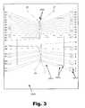
- FIG. 3is an illustration of a top-view of an unpackaged semiconductor chip with inline central pads connected to a PC board base according to one embodiment of the present invention.
- FIG. 4 ais a perspective side view of a Chip-on-Board memory module according to one embodiment of the present invention.
- FIG. 4 bis a close-up cross-sectional view of an unpackaged part mounted to a PC board according to one embodiment of the present invention.
- FIG. 5is a block diagram illustrating a layout of major components of a Chip-on-Board memory module fabricated using patching networks according to one embodiment of the present invention.
- FIG. 6is an illustrative cross-sectional view of a shielded Chip-on-Board memory module according to one embodiment of the present invention.
- FIG. 7is an illustrative top-view of a Chip-on-Board memory module according to one embodiment of the present invention.
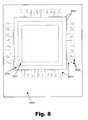
- FIG. 8is an illustration of a top-view of an unpackaged semiconductor chip with pads connected to a PC board base, according to another embodiment of the present invention.
- FIG. 9is a flowchart illustrating a method of mounting unpackaged semiconductor chips according to another embodiment of the present invention.
- Chip-on-Board memory modules fabricated using partially-defective memory parts or a combination of partially-defective and flawless memory partsare disclosed herein.
- a combination of memory partswhich in one embodiment includes at least one unpackaged chip, are mounted on a printed circuit board and tested.
- a number of fabrication benefitsare facilitated, e.g., unpackaged chips are easily oriented, bonding wires are secured, memory chips may be removed if necessary, etc.
- a number of different circuit boards, memory parts, and patching techniquesresult in a variety of functional modules. Additionally, a cover may be used as part of the module for aesthetic value and protection of fragile parts, leads, wires, etc.
- the embodiments describedinvolve an effective utilization of semiconductor chips or die which both benefit the semiconductor manufacturers by reducing their production losses and various electronic system manufacturers which are often able to utilize lower cost memory and subcomponents manufactured using less-than-flawless semiconductor memories.
- FIG. 1is a flowchart illustrating a method of assembling a Chip-on-Board memory module. As shown in FIG. 1, the method may be divided into several areas or steps: mounting (step 100 ), patching (step 110 ), testing (step 120 ), and covering (step 130 ).
- step 100During mounting (step 100 ), preferably, at least one unpackaged chip is mounted on a printed circuit board.
- a selectively settable materialmay be used to mount unpackaged memory parts. More specifically, selectively settable liquids, such as adhesives made by Dymax Corporation, are used, in some examples, to tack die to a PC board.
- UV materiali.e., material hardened by exposure to certain wavelengths of light
- different wavelengths of lightmay cause different levels of hardness. For example, light with 700 nm (nanometers) wavelength may cause a certain liquid UV material to thicken, while light at 1000 nm causes the UV material to permanently harden.
- tools that dispense UV material and emit lightmay be used in the process. Such tools include the PC-3D made by Dymax.
- a ring of selectively settable materialis preferably used to surround the die and hold the die in place.
- the alignment of each unpackaged chipmay be adjusted (step 102 ), after which the ring of selectively settable material disposed around the chip is cured or hardened (step 103 ).
- the hardened ring around each diekeeps the die in place.
- the ringis higher than the die it surrounds to facilitate the addition of bond wires.
- a layer of selectively settable materialis placed between each die and the PC board.
- the same settable material that is used between each die and the PC boardmay also be used around each die or two different selectively settable materials may be used.
- the selectively settable material used between the die and the PC boardshould have a higher curing temperature than the material used around the die.
- This configurationallows the material around the die to be hardened, while the material between the die and the PC board remains liquid.
- UV materialwhen using UV material, light at a specified wavelength will harden the ring around the die, while the material between the die and the PC board remains liquid.
- using two different materialsallows a memory part to be firmly tacked to the PC board, while being buffered, or padded, physically and thermally from the surface of the PC board to which it is mounted.
- caremay be taken to harden only the outer ring of the selectively settable material.
- a second ring (or layer) of selectively settable materialmay also be added (step 104 ) on top of the first ring of selectively settable material.
- This second ringis used to capture the wires, known as bonding wires, which electrically connect the die to the conductive pads of the PC board.
- the wiresmay be captured by carefully placing the wires within the second ring while the selectively settable material is still manageable and then hardening the ring. The use of the second ring prevents the wires from touching the die or other wires.
- the memory unitcan be loaded into a bonding machine that locates each die and, using an automated program, bonds the wires to the contact pads on the die and the PC board (step 105 ).
- step 106After the wires are bonded, connecting the die to the module, a visual inspection of the wires is made (step 106 ). If there are any missing or broken wires (determination 107 ), a manual adjustment of the bonds (step 108 ) is used to correct the problem. The unit is visually inspected again (step 107 ), and if there are no missing or broken wires (determination 107 ), a small amount of selectively settable material is placed over the wires and hardened (step 109 ).
- Chip-on-Board memory modulemay be mounted by soldering the leads of the package to pads on the circuit board. Specific pads on the PC board are usually designed purposely for use with packaged or unpackaged parts.
- a “Chip-on-Board” PC boardmay contain any combination of pads utilizable for connecting memory devices to the PC board. Preferably, at least one set of pads is designed for use with an unpackaged part or device.
- the patching processbegins.
- the moduleis first tested (step 111 ) using a series of read/write functionality tests, and defective I/O lines are identified. If the defective parts can be patched (determination 112 ), the patching technique corresponding to the particular memory product and PC board layout is used to patch the defective parts (step 114 ).
- the patching processes of U.S. Pat. No. 6,119,049 and co-pending patent application, “Method and Apparatus for Patching Memory Modules,”may be used.
- All patching techniquesrequire the disconnection of failed I/O lines and the connection of other unused, functional I/O lines.
- the disconnection and connectionmay be accomplished by adding or removing solder, called solder-dots.
- Another alternativeis to add or remove a jumper wires.
- step 113If there are not enough bits to patch the defective parts (determination 111 ), one or more low value parts, i.e., parts with few operable I/O lines, must be replaced with higher value parts (step 113 ) to provide sufficient bits for a fully-functional module.
- the “value” of a memory partrefers to the proportion of functioning, as opposed to non-functioning, input/output lines.
- a higher value part, used to replace a low value part,must pass through the mounting process (step 100 ) before the module can continue on to the patching process (step 110 ).
- the modulegoes through a testing process (step 120 ).
- the moduleis first placed under a high heat and high voltage test called burn-in (step 114 ).
- the burn-in test(step 114 ) accelerates the aging process of the electronics and may cause “early-life” failures to occur in the oven. If a fail occurs during burn-in (determination 122 ), the patching process (step 110 ), and if needed the mounting process (step 100 ), is repeated until a module passes the burn-in test (determination 122 ).
- testerswhich may be used to test memory in the form of die, chips (packaged parts), and modules. Such testers are commonly known in the art. Additionally, commercially available machines used for burn-in tests, bonding wire installation, etc., are commonly known in the art.
- step 123an industry standard parameter test, called a “four-corner” test, is performed (step 123 ), testing the combinations: high voltage/high signal level, high voltage/low signal level, low voltage/high signal level, and low voltage/low signal level. This test assures memory modules that pass a number of subsequent pattern tests (step 123 ) will run the same on any motherboard.
- the patching process (step 110 ) and testing process (step 120 )are repeated until a module passes the parameter and pattern tests (determination 124 ).
- a covercan then be added (step 131 ) to protect the memory parts and all exposed circuitry on the surface of the PC board.
- the coverprovides ESD (Electrostatic Discharge) protection to the module, but does not act as a heat sink, i.e., the cover does not touch the memory parts.
- the process of FIG. 1may be carried out using automated machinery for fabrication, patching, and testing purposes.
- automated machinesare programmed to dispense one or more selectively settable liquids, mount memory parts to a PC board, connect I/O bit lines to I/O output lines, perform functionality tests, attach the protective cover, etc.
- the dispensing of selectively settable liquids, mounting of memory parts to a PC board, connecting I/O bit lines to I/O output lines, performing functionality tests as described above, mounting a protective cover, etc.may be performed manually.
- Another embodiment of the Chip-on-Board fabrication process, shown in FIG. 1,uses a combination of automated and manual labor.
- FIG. 2is a schematic diagram of a memory part that may be used to build a memory module as described herein.
- the memory part ( 200 )may be represented by a block ( 201 ) and a number of labeled pins ( 202 ).
- the memory part itself ( 200 )may be any size or shape, and the pins ( 202 ) may be located at any location on the surface of the semiconductor material from which the memory part ( 200 ) is made.
- a variety of signalsfunction together to read data and write data using a memory part ( 200 ).
- these signalsallow a host device to activate a memory part ( 200 ), access a particular memory segment defined by row and column, write information to the memory cells, read information from the memory cells, etc.
- FIG. 3is an illustration of a top-view of an unpackaged memory chip with in-line central pads connected to a printed circuit board base.
- the input and output signalse.g., the signals of Table 1
- the input and output signalsmay be connected to a host device by bonding wires ( 303 ) between pads ( 304 ) of the unpackaged memory part ( 301 ) to pads ( 302 ) on a circuit board ( 305 ).
- the pads ( 302 ) of the circuit board ( 305 )may be pre-wired to allow a host device to effectively utilize the memory part ( 301 ).
- the memory part ( 301 ) of FIG. 3is an illustration of a physical embodiment of the memory part ( 200 ) schematic of FIG. 2 attached to a PC board.
- the pin numbers ( 202 ) of FIG. 2, representing particular signals,are also illustrated in FIG. 3.
- FIG. 4 ais a perspective side view of a Chip-on-Board memory module.
- an unpackaged memory part ( 402 )is attached to a PC board ( 401 ), and wires ( 403 ) connect the signals of the memory part ( 402 ) to the circuit board ( 401 ).
- a selectively settable liquid ( 404 )is dispensed around the die ( 402 ), wires ( 403 ), pads, etc., and hardened.
- FIG. 4 bis a close-up cross-sectional view of an unpackaged part mounted to a PC board.
- an unpackaged part ( 402 )is mounted to a PC board ( 401 ) using several sections of selectively settable material.
- a first section of selectively settable material ( 414 )is placed between the die ( 402 ) and the PC board ( 401 ).
- this first section of selectively settable material ( 414 )remains liquid and provides a physical and thermal pad between the die ( 402 ) and PC board ( 401 ).
- a ring (or layer) of selectively settable material ( 413 )is placed around the perimeter of the unpackaged part ( 402 ). After the unpackaged part ( 402 ) is correctly oriented, the ring of selectively settable material ( 413 ) is hardened, thereby tacking the die ( 402 ) to the PC board ( 401 ). Additionally, the height of this first layer ( 413 ) may be higher than the die ( 402 ), thus allowing bonding wires to rest on the first layer ( 413 ) without touching the die ( 402 ).
- the first ring of selectively settable material ( 413 )may be covered with a second ring (or layer) of selectively settable material ( 416 ).
- a second ring (or layer) of selectively settable material ( 416 )By placing part of the bonding wires ( 414 ) within the second layer of selectively settable material ( 416 ) and hardening the second layer ( 416 ), the wires ( 414 ) may be captured.
- the process of connecting bonding wires between a die ( 402 ) and a PC board ( 401 )is greatly facilitated. During this process, care should be taken to separate each bonding wire ( 414 ) within the second ring of selectively settable material ( 416 ) to avoid shorting wires ( 414 ) together.
- FIG. 5is a block diagram illustrating a layout of major components of a Chip-on-Board memory module fabricated using patching networks.
- the memory module ( 500 )comprises a printed circuit board ( 501 ), unpackaged, memory parts ( 502 ), patching networks ( 503 ), resistor elements ( 504 ), capacitor elements ( 505 ), and interface connections ( 506 ).
- a memory module ( 500 )may include packaged memory parts ( 507 ).
- other electrical componentse.g., voltage regulators, inductors, phase locked loop units, differential clock drivers, etc., may be mounted to the circuit board ( 501 ).
- the printed circuit board ( 501 )uses several different layers to create a complex network of electrical paths and connection points purposefully designed to allow the fabrication of a functional memory product using the patching networks ( 503 ) and partially-defective memory parts ( 502 , 507 ).
- memory productsthere are a variety of memory products that may be assembled using the module ( 500 ) illustrated in FIG. 5, e.g., Single Inline Memory Module (SIMM), Dual Inline Memory Module (DIMM), Dynamic Random Access Memory (DRAM), Synchronous Dynamic Random Access Memory (SDRAM), etc.
- memory partse.g., the memory part of FIG. 2, enable a host device to store and access one or more bits, i.e., an electronic, or logic, 1 or 0.
- a single bit or group of bits, i.e., byte, word, etc., stored and accessible in memoryprovide information significant to the host device and software applications running on the host device.
- the I/O signalse.g., DQ(x:0) in Table 1, of the memory parts ( 502 , 507 ; FIG. 5) are connected to one or more patching networks ( 503 ).
- the patching networks ( 503 )comprise a collection of traces, etc., that allow one I/O signal line to be substituted with another I/O signal line by manually or automatically changing the connection at one or more designated locations.
- the patching solutionuses more controllable memory parts ( 502 , 507 ) than past patching solutions, e.g., the solutions presented in U.S. Pat. No. 6,119,049, to accomplish another process for patching memory parts.
- Some examples of patching networks that maybe usedinclude 2-to-1, 4-to-1, and 8-to-1 patching networks as described in the co-pending patent application entitled, “New Methods and Apparatus for Patching Memory Modules.”
- the memory parts ( 502 , 507 ) shown in FIG. 5allow the host device to provide a number of additional read/write control signals, e.g., DQM# in Table 1, that eliminate the need to steer CAS (Column Address Select) and RAS (Row Address Select) signals to the memory parts ( 502 , 507 ) used for patching.
- memory parts ( 502 , 507 ) that are used to substitute failed memory outputsshare the same read/write control signals as the memory part ( 502 , 507 ) whose output they are replacing.
- Typical memory partsinclude 8M ⁇ 8, 16M ⁇ 8, and 32M ⁇ 8 memory parts commonly used in the art to build memory modules.
- all I/O signalsare sent through resistance networks ( 504 ) that provide a buffer between the memory part ( 502 , 507 ) and the host device accessing the memory.
- Another component of the memory module ( 500 )is a group of capacitors ( 505 ), which serve to stabilize the power supply signal for each memory part ( 502 , 507 ) by removing most high frequency electrical noise that may occur.
- the interface connections ( 506 )enable the memory module ( 500 ) to be conveniently plugged into an appropriate connection device of a host device. Through the connection, the host device is able to interact with the memory module ( 500 ) as herein above described, etc.
- patching networks ( 503 ) and processesa reference may be made to U.S. Pat. No. 6,119,049 and the co-pending patent application, entitled, “Improved Patching Methods and Apparatus for Fabricating Memory Modules.”
- FIG. 6is an illustrative cross-sectional view of a shielded Chip-on-Board memory module.
- the module ( 600 )uses a PC board ( 601 ) as a base. Attached to the PC board ( 601 ) are packaged parts ( 602 ) and unpackaged parts ( 603 ). In particular, any combination of packaged parts ( 602 ) and unpackaged parts ( 603 ) may be used. In some embodiments, at least one unpackaged part is used ( 603 ).
- Covering the memory parts (and any other electronics, leads, wires, etc.)is a cover ( 804 ), which may be mounted to the PC board ( 601 ). In at least one embodiment, there is no electrical or physical contact between the cover ( 604 ) and the memory parts ( 602 , 603 ) such that the cover ( 604 ) does not act as a heat sink for the memory parts ( 602 , 603 ).
- the cover ( 604 )advantageously increases the security and aesthetic appearance of the module ( 600 ).
- FIG. 7is an illustrative top-view of a Chip-on-Board memory module.
- a cover ( 704 )is attached on one or both sides of the module ( 700 ) using rivets ( 707 ), or other fasteners, that attach the cover ( 704 ) to the PC board ( 901 ).
- a ground plane of the PC board ( 701 )may be made to connect to one or more rivets ( 707 ) touching the cover ( 704 ), thus providing a means of discharging any electrostatic charges, i.e., ESD (Electrostatic Discharge), that could potentially damage the module ( 700 ).
- ESDElectrostatic Discharge
- the cover ( 704 )also provides physical protection to any electronics, wires, etc., used to create the memory module ( 700 ).
- the modulemay be connected to any device, e.g., the motherboard of a host device, equipped to read and write information to the particular memory module ( 700 ).
- FIG. 8is an illustration of a top-view of an unpackaged semiconductor chip with perimeter pads connected to a PC board base.
- an unpackaged semiconductor chip ( 801 )may be attached to a PC board ( 805 ) in similar fashion as shown in FIG. 3, wherein bonding wires ( 803 ) may be attached between pads ( 804 ) of the unpackaged chip ( 801 ) and pads ( 802 ) of the PC board ( 805 ).
- FIG. 8shows another configuration of pads ( 804 ) on an unpackaged part ( 801 ), wherein the pads ( 804 ) are distributed around the perimeter of the unpackaged part ( 801 ). More specifically, an outer layer of pads ( 806 ) and an inner layer of pads ( 807 ) are shown in FIG. 8.
- the arrangement of perimeter pads ( 804 ) shown in FIG. 8is in contrast to other pad configurations, e.g., the inline central pads shown for the die of FIG. 3.
- the use of selectively settable materialmay greatly facilitate the process of attaching bonding wires to unpackaged chips for any variety of pad configurations.
- bonding wirescan be positioned, physically separated from other wires, readjusted, protected, etc.
- FIG. 9is a flowchart illustrating a method of mounting an unpackaged semiconductor chip with perimeter pads. As shown, the method of FIG. 9 is similar to the mounting method (step 100 , FIG. 1) shown in FIG. 1. In particular, the method of FIG. 9 illustrates a method of mounting unpackaged semiconductor parts, e.g., the unpackaged part ( 801 , FIG. 8) shown in FIG. 8, which have one or more layers of pads around the perimeter of the unpackaged part.
- the unpackaged semiconductor partse.g., the unpackaged part ( 801 , FIG. 8) shown in FIG. 8, which have one or more layers of pads around the perimeter of the unpackaged part.
- the methodcomprises mounting a die on a PC board (step 901 ). This may be accomplished as described for FIG. 1, wherein the alignment of each unpackaged chip is adjusted (step 902 ), after which a ring of selectively settable material disposed around the chip is cured or hardened (step 903 ). The hardened ring around each die keeps the die in place.
- a layer of selectively settable materialis placed between each die and the PC board.
- the same settable material that is used between each die and the PC boardmay also be used around each die or two different selectively settable materials are used as described above.
- a bondermay then attach wires between the outer pads of the unpackaged part and pads on a PC board (step 904 ), as illustrated in FIG. 8.
- a layer of selectively settable materialmay be used to cover the bonding wires attached to the outer pads of the unpackaged part (step 905 ).
- a bonding machinemay attach wires between the inner pads of an unpackaged part and pads of a PC board (step 906 ).
- step 906After attaching bonding wires between the inner pads of the unpackaged part and pads of a PC board (step 906 ), another layer of selectively settable material may be added to cover the inner layer of wires and pads (step 907 ).
- step 907After the wires are bonded (steps 904 , 906 ), and selectively settable material separates and covers these wires (steps 905 , 907 ), a visual inspection of the wires is made (step 908 ). If there are any problems (determination 909 ), e.g., wires that are broken, shorted, out of place, etc., a manual adjustment of the wires and bonds may be used to correct the problem (step 910 ). The unit may then be visually inspected again (step 908 ), and if there are no problems (determination 909 ), the selectively settable material, which covers the wires and pads, is completely hardened (step 911 ).
- the process of FIG. 9may be carried out using automated machinery for fabrication, etc.
- automated machinesare programmed to dispense one or more selectively settable liquids, mount unpackaged parts to a PC board, bond wires between unpackaged parts and a PC board, perform functionality tests, etc.
- the dispensing of selectively settable liquids, mounting of unpackaged parts to a PC board, and performing functionality tests as described abovemay be performed manually.
- Another embodiment of the Chip-on-Board fabrication process, shown in FIG. 9,uses a combination of automated manual labor.
- selectively settable materialmay advantageously be used as a thermal and physical buffer between an unpackaged part and a PC board.
- one or more layers of selectively settable materialmay effectively be used to capture bonding wires attached to unpackaged semiconductor parts, which use a variety of pad configurations. As illustrated above, pads on an unpackaged semiconductor part may be placed in the center of a die (as shown in FIG. 3), around the perimeter of a die (as shown in FIG. 8), or any other configuration.
Landscapes
- Engineering & Computer Science (AREA)
- Computer Hardware Design (AREA)
- Microelectronics & Electronic Packaging (AREA)
- Power Engineering (AREA)
- Nanotechnology (AREA)
- Chemical & Material Sciences (AREA)
- Physics & Mathematics (AREA)
- Mathematical Physics (AREA)
- Theoretical Computer Science (AREA)
- Crystallography & Structural Chemistry (AREA)
- Manufacturing & Machinery (AREA)
- Condensed Matter Physics & Semiconductors (AREA)
- General Physics & Mathematics (AREA)
- Semiconductor Memories (AREA)
- Encapsulation Of And Coatings For Semiconductor Or Solid State Devices (AREA)
Abstract
Description
- The present invention claims the filing date of U.S. Provisional Patent 60/360,036, filed on Feb. 26, 2002, and references the related U.S. patent application Attorney Docket No. 65887-0006, entitled “Improved Patching Methods and Apparatus for Fabricating Memory Modules,” filed Feb. 20, 2003, both of which are herein incorporated by this reference.[0001]
- Selected embodiments of the present invention relate to electronic logic modules that use unpackaged die. More specifically, embodiments of the present invention relate to fabrication processes for Chip-on-Board modules.[0002]
- Semiconductor manufacturing processes have become increasingly more complex. From the beginning with the creation of discrete transistors and other semiconductor devices through subsequent medium and large scale integrated devices, the number of transistors or independent elements which can fit on to a semiconductor chip has grown exponentially each year. For example, the first integrated processors comprised on the order of 2300 transistors. A recently announced integrated circuit processor comprises more than 220 million transistors. Other circuits are projected to contain over 1 billion transistors in the foreseeable future.[0003]
- This continued exponential growth of semiconductor manufacturing processes, while contributing to the greatly decreased costs of individual semiconductor devices and products has also exacerbated many production and testing problems associated with commercial semiconductor manufacturing processes. The substantial increase in the density of electronic circuits in the semiconductor integrated manufacturing processes has resulted in the production of many more less-than-perfect semiconductor die or chips. This increase in the production of less than perfect chips and die has spawned a new market for electronic component sellers who find ways to utilize less-than-perfect chips or die to assemble working components.[0004]
- The many enhancements and advancements in semiconductor manufacturing and packaging processes have resulted in the creation of a number of price sensitive semiconductor product applications for electronic parts sellers. In particular, these electronic parts sellers develop low cost memory modules or other semiconductor devices through the utilization of cost effective processes, including less-than-perfect semiconductor parts.[0005]
- One method of building memory modules using partially-defective memory parts may use unpackaged semiconductor memories, or die, for all or part of the memory parts used to build a memory module. Using die instead of packaged parts increases the complexity of the fabrication process, but provides substantial savings by eliminating the cost of packaging parts. The use of unpackaged parts to build memory modules, or other electronics, is called Chip-on-Board, or COB. In recent years, improvements in semiconductor memory technology and manufacturing have led to the creation of new memory products and patching techniques implemented using a Chip-on-Board process.[0006]
- While the process used to assemble Chip-on-Board modules, referring to the process disclosed in U.S. Pat. No. 6,119,049, is effective, modem adhesives provide new methods of mounting unpackaged parts. In particular, an improvement in the yield of Chip-on-Board memory modules can be attained by using one or more selectively settable liquids. A standard burn-in process used to test electronic memory modules (including Chip-on-Board modules) under high heat and high voltage stress may frequently cause a number of failed and broken chips, due mostly to a difference in the thermal expansion coefficients of the chips and the circuit board base. By using one or more selectively settable liquids to provide a thermal and physical buffer (pad) between an unpackaged part and a printed circuit board, heat expansion stress can be reduced.[0007]
- In summary, there is an ongoing need in the art for means and methods of producing low cost semiconductor devices, particularly memory modules. Related to this is an ongoing need to make use of semiconductor devices that are partially-defective so that such device are not completely wasted. The use of unpackaged parts, including new mounting techniques, is desirable to provide important cost saving practices.[0008]
- Among many possible embodiments, the present invention provides a number of Chip-on-Board memory modules fabricated using a variety of patching methods and a new and novel mounting process. Each Chip-on-Board memory module preferably uses partially-defective memory parts or a combination of partially-defective and flawless memory parts.[0009]
- Another embodiment of the present invention includes mounting unpackaged electronic parts, not limited to memory parts, using one or more selectively settable liquids. By tacking an unpackaged electronic part to a circuit board base, hereafter described as a PC board, using one or more selectively settable liquids, part adjustments such as repositioning, removal, and bonding wire installation are greatly expedited and facilitated.[0010]
- Another embodiment of the present invention encompasses a variety of memory modules, including, Dynamic Random Access Memory (DRAM), Synchronous Dynamic Random Access Memory (SDRAM), Double Data Rate (DDR), etc., created using the presently described Chip-on-Board fabrication method. These modules may use a number of patching methods, e.g., the methods described in U.S. Pat. No. 6,119,049. Additionally, new patching methods are described in the above referenced patent application, “Methods and Apparatus for Patching Memory Modules,” which is co-pending and of common ownership with the present application by U.S. Pat. No. 6,119,049 inventor, Charles I. Peddle, and may be used to fabricate the Chip-on-Board memory modules.[0011]
- The accompanying drawings illustrate various embodiments of the present invention and are a part of the specification. Together with the following description, the drawings demonstrate and explain the principles of the present invention. The illustrated embodiments are examples of the present invention and do not limit the scope of the invention.[0012]
- FIG. 1 is a flowchart illustrating a method of manufacturing Chip-on-Board memory modules according to one embodiment of the present invention.[0013]
- FIG. 2 is a schematic diagram illustrating a memory part that may be used to fabricate a memory module according to one embodiment of the present invention.[0014]
- FIG. 3 is an illustration of a top-view of an unpackaged semiconductor chip with inline central pads connected to a PC board base according to one embodiment of the present invention.[0015]
- FIG. 4[0016]ais a perspective side view of a Chip-on-Board memory module according to one embodiment of the present invention.
- FIG. 4[0017]bis a close-up cross-sectional view of an unpackaged part mounted to a PC board according to one embodiment of the present invention.
- FIG. 5 is a block diagram illustrating a layout of major components of a Chip-on-Board memory module fabricated using patching networks according to one embodiment of the present invention.[0018]
- FIG. 6 is an illustrative cross-sectional view of a shielded Chip-on-Board memory module according to one embodiment of the present invention.[0019]
- FIG. 7 is an illustrative top-view of a Chip-on-Board memory module according to one embodiment of the present invention.[0020]
- FIG. 8 is an illustration of a top-view of an unpackaged semiconductor chip with pads connected to a PC board base, according to another embodiment of the present invention.[0021]
- FIG. 9 is a flowchart illustrating a method of mounting unpackaged semiconductor chips according to another embodiment of the present invention.[0022]
- Throughout the drawings, identical reference numbers designate similar, but not necessarily identical, elements.[0023]
- Chip-on-Board memory modules fabricated using partially-defective memory parts or a combination of partially-defective and flawless memory parts are disclosed herein. A combination of memory parts, which in one embodiment includes at least one unpackaged chip, are mounted on a printed circuit board and tested. By using one or more selectively settable liquids to mount unpackaged memory chips, a number of fabrication benefits are facilitated, e.g., unpackaged chips are easily oriented, bonding wires are secured, memory chips may be removed if necessary, etc. A number of different circuit boards, memory parts, and patching techniques result in a variety of functional modules. Additionally, a cover may be used as part of the module for aesthetic value and protection of fragile parts, leads, wires, etc.[0024]
- The embodiments described involve an effective utilization of semiconductor chips or die which both benefit the semiconductor manufacturers by reducing their production losses and various electronic system manufacturers which are often able to utilize lower cost memory and subcomponents manufactured using less-than-flawless semiconductor memories.[0025]
- FIG. 1 is a flowchart illustrating a method of assembling a Chip-on-Board memory module. As shown in FIG. 1, the method may be divided into several areas or steps: mounting (step[0026]100), patching (step110), testing (step120), and covering (step130).
- During mounting (step[0027]100), preferably, at least one unpackaged chip is mounted on a printed circuit board. In some embodiments, a selectively settable material may be used to mount unpackaged memory parts. More specifically, selectively settable liquids, such as adhesives made by Dymax Corporation, are used, in some examples, to tack die to a PC board.
- While many types of adhesives may be used to tack unpackaged die to a PC board, UV material, i.e., material hardened by exposure to certain wavelengths of light, is used in selected embodiments. When using UV material, different wavelengths of light may cause different levels of hardness. For example, light with 700 nm (nanometers) wavelength may cause a certain liquid UV material to thicken, while light at 1000 nm causes the UV material to permanently harden. Accordingly, tools that dispense UV material and emit light may be used in the process. Such tools include the PC-3D made by Dymax.[0028]
- When mounting die on a PC board (step[0029]101), a ring of selectively settable material is preferably used to surround the die and hold the die in place. Once mounted, the alignment of each unpackaged chip may be adjusted (step102), after which the ring of selectively settable material disposed around the chip is cured or hardened (step103). The hardened ring around each die keeps the die in place. In some embodiments, the ring is higher than the die it surrounds to facilitate the addition of bond wires.
- A layer of selectively settable material is placed between each die and the PC board. In one embodiment, the same settable material that is used between each die and the PC board may also be used around each die or two different selectively settable materials may be used.[0030]
- More specifically, the selectively settable material used between the die and the PC board should have a higher curing temperature than the material used around the die. This configuration allows the material around the die to be hardened, while the material between the die and the PC board remains liquid. For example, when using UV material, light at a specified wavelength will harden the ring around the die, while the material between the die and the PC board remains liquid. In other words, using two different materials allows a memory part to be firmly tacked to the PC board, while being buffered, or padded, physically and thermally from the surface of the PC board to which it is mounted. Alternatively, if the same selectively settable material is used underneath and around the die, care may be taken to harden only the outer ring of the selectively settable material.[0031]
- A second ring (or layer) of selectively settable material may also be added (step[0032]104) on top of the first ring of selectively settable material. This second ring is used to capture the wires, known as bonding wires, which electrically connect the die to the conductive pads of the PC board. The wires may be captured by carefully placing the wires within the second ring while the selectively settable material is still manageable and then hardening the ring. The use of the second ring prevents the wires from touching the die or other wires. After the bonding wires are captured, the memory unit can be loaded into a bonding machine that locates each die and, using an automated program, bonds the wires to the contact pads on the die and the PC board (step105).
- After the wires are bonded, connecting the die to the module, a visual inspection of the wires is made (step[0033]106). If there are any missing or broken wires (determination107), a manual adjustment of the bonds (step108) is used to correct the problem. The unit is visually inspected again (step107), and if there are no missing or broken wires (determination107), a small amount of selectively settable material is placed over the wires and hardened (step109).
- Any packaged parts used on a Chip-on-Board memory module may be mounted by soldering the leads of the package to pads on the circuit board. Specific pads on the PC board are usually designed purposely for use with packaged or unpackaged parts. As used herein, a “Chip-on-Board” PC board may contain any combination of pads utilizable for connecting memory devices to the PC board. Preferably, at least one set of pads is designed for use with an unpackaged part or device.[0034]
- After the memory parts have been mounted (step[0035]100), the patching process (step110) begins. Preferably, the module is first tested (step111) using a series of read/write functionality tests, and defective I/O lines are identified. If the defective parts can be patched (determination112), the patching technique corresponding to the particular memory product and PC board layout is used to patch the defective parts (step114). As herein above mentioned, the patching processes of U.S. Pat. No. 6,119,049 and co-pending patent application, “Method and Apparatus for Patching Memory Modules,” may be used.
- All patching techniques require the disconnection of failed I/O lines and the connection of other unused, functional I/O lines. The disconnection and connection may be accomplished by adding or removing solder, called solder-dots. Another alternative is to add or remove a jumper wires.[0036]
- If there are not enough bits to patch the defective parts (determination[0037]111), one or more low value parts, i.e., parts with few operable I/O lines, must be replaced with higher value parts (step113) to provide sufficient bits for a fully-functional module. As used herein, the “value” of a memory part refers to the proportion of functioning, as opposed to non-functioning, input/output lines. A higher value part, used to replace a low value part, must pass through the mounting process (step100) before the module can continue on to the patching process (step110).
- After a suitable combination of memory parts and patches provides a functional module, the module goes through a testing process (step[0038]120). Preferably, the module is first placed under a high heat and high voltage test called burn-in (step114). The burn-in test (step114) accelerates the aging process of the electronics and may cause “early-life” failures to occur in the oven. If a fail occurs during burn-in (determination122), the patching process (step110), and if needed the mounting process (step100), is repeated until a module passes the burn-in test (determination122).
- As indicated above, the uncured adhesive liquid that remains under a select memory die serves as a thermal and physical buffer between the die and the PC board. This buffer may be valuable during the burn-in test to prevent damage to the unit caused by unequal thermal expansion coefficients of the die and the PC board.[0039]
- There are a number of commercially available testers, which may be used to test memory in the form of die, chips (packaged parts), and modules. Such testers are commonly known in the art. Additionally, commercially available machines used for burn-in tests, bonding wire installation, etc., are commonly known in the art.[0040]
- Once a module passes the burn-in test (determination[0041]122), an industry standard parameter test, called a “four-corner” test, is performed (step123), testing the combinations: high voltage/high signal level, high voltage/low signal level, low voltage/high signal level, and low voltage/low signal level. This test assures memory modules that pass a number of subsequent pattern tests (step123) will run the same on any motherboard.
- If the module fails either the parameter test or the pattern test (determination[0042]124), the patching process (step110) and testing process (step120) are repeated until a module passes the parameter and pattern tests (determination124).
- If desired, a cover can then be added (step[0043]131) to protect the memory parts and all exposed circuitry on the surface of the PC board. In some embodiments, the cover provides ESD (Electrostatic Discharge) protection to the module, but does not act as a heat sink, i.e., the cover does not touch the memory parts.
- The process of FIG. 1 may be carried out using automated machinery for fabrication, patching, and testing purposes. In one embodiment, automated machines are programmed to dispense one or more selectively settable liquids, mount memory parts to a PC board, connect I/O bit lines to I/O output lines, perform functionality tests, attach the protective cover, etc. In another embodiment, the dispensing of selectively settable liquids, mounting of memory parts to a PC board, connecting I/O bit lines to I/O output lines, performing functionality tests as described above, mounting a protective cover, etc., may be performed manually. Another embodiment of the Chip-on-Board fabrication process, shown in FIG. 1, uses a combination of automated and manual labor.[0044]
- FIG. 2 is a schematic diagram of a memory part that may be used to build a memory module as described herein. As shown in FIG. 2, the memory part ([0045]200) may be represented by a block (201) and a number of labeled pins (202). The memory part itself (200) may be any size or shape, and the pins (202) may be located at any location on the surface of the semiconductor material from which the memory part (200) is made. There are many types of memory units and technologies, e.g., DRAM, SDRAM, Single Inline Memory Module (SIMM), Dual Inline Memory Module (DIMM), BGA (Ball Grid Array), etc. In general, these memory units and technologies perform the same functions, and are described by Table 1.
TABLE 1 Symbol Type Description A[n:0] Input-Synchronous Pin definitions; a function of array size CLK Input-Clock Master Clock input CKE Input-Clock Enable Activates CLK when high, deactivates when low RAS# Input-Synchronous Row address strobe CS# Input-Synchronous Selects chip when active CAS# Input-Synchronous Column address strobe WE# Input-Synchronous Write enable strobe DQM# Read mode - controls the data output buffers DQML/H# Input-Synchronous Write mode - masks data from being written DQ(x:0) Input/Output-Synchronous Data I/O pins Vcc, Vss Power pins Supply pins for the core VccQ, VssQ Power pins Supply pins for the output buffers - As shown in Table 1, a variety of signals function together to read data and write data using a memory part ([0046]200). In particular, these signals allow a host device to activate a memory part (200), access a particular memory segment defined by row and column, write information to the memory cells, read information from the memory cells, etc.
- FIG. 3 is an illustration of a top-view of an unpackaged memory chip with in-line central pads connected to a printed circuit board base. As shown in FIG. 3, the input and output signals, e.g., the signals of Table 1, may be connected to a host device by bonding wires ([0047]303) between pads (304) of the unpackaged memory part (301) to pads (302) on a circuit board (305). The pads (302) of the circuit board (305) may be pre-wired to allow a host device to effectively utilize the memory part (301). Specifically, the memory part (301) of FIG. 3 is an illustration of a physical embodiment of the memory part (200) schematic of FIG. 2 attached to a PC board. As illustrated, the pin numbers (202) of FIG. 2, representing particular signals, are also illustrated in FIG. 3.
- FIG. 4[0048]ais a perspective side view of a Chip-on-Board memory module. As shown in FIG. 4a, an unpackaged memory part (402) is attached to a PC board (401), and wires (403) connect the signals of the memory part (402) to the circuit board (401). In order to protect the wires (403) and unpackaged die (402), a selectively settable liquid (404) is dispensed around the die (402), wires (403), pads, etc., and hardened.
- FIG. 4[0049]bis a close-up cross-sectional view of an unpackaged part mounted to a PC board. As shown in FIG. 4b, an unpackaged part (402) is mounted to a PC board (401) using several sections of selectively settable material. A first section of selectively settable material (414) is placed between the die (402) and the PC board (401). In some embodiments, this first section of selectively settable material (414) remains liquid and provides a physical and thermal pad between the die (402) and PC board (401).
- In order to tack the unpackaged part ([0050]402) to the PC board (401) a ring (or layer) of selectively settable material (413) is placed around the perimeter of the unpackaged part (402). After the unpackaged part (402) is correctly oriented, the ring of selectively settable material (413) is hardened, thereby tacking the die (402) to the PC board (401). Additionally, the height of this first layer (413) may be higher than the die (402), thus allowing bonding wires to rest on the first layer (413) without touching the die (402).
- After being hardened, the first ring of selectively settable material ([0051]413) may be covered with a second ring (or layer) of selectively settable material (416). By placing part of the bonding wires (414) within the second layer of selectively settable material (416) and hardening the second layer (416), the wires (414) may be captured. By trapping the wires (414), the process of connecting bonding wires between a die (402) and a PC board (401) is greatly facilitated. During this process, care should be taken to separate each bonding wire (414) within the second ring of selectively settable material (416) to avoid shorting wires (414) together.
- FIG. 5 is a block diagram illustrating a layout of major components of a Chip-on-Board memory module fabricated using patching networks. As shown in FIG. 5, the memory module ([0052]500) comprises a printed circuit board (501), unpackaged, memory parts (502), patching networks (503), resistor elements (504), capacitor elements (505), and interface connections (506). In another embodiment of the invention, a memory module (500) may include packaged memory parts (507). Additionally, other electrical components, e.g., voltage regulators, inductors, phase locked loop units, differential clock drivers, etc., may be mounted to the circuit board (501).
- The printed circuit board ([0053]501) uses several different layers to create a complex network of electrical paths and connection points purposefully designed to allow the fabrication of a functional memory product using the patching networks (503) and partially-defective memory parts (502,507).
- There are a variety of memory products that may be assembled using the module ([0054]500) illustrated in FIG. 5, e.g., Single Inline Memory Module (SIMM), Dual Inline Memory Module (DIMM), Dynamic Random Access Memory (DRAM), Synchronous Dynamic Random Access Memory (SDRAM), etc. In general, memory parts, e.g., the memory part of FIG. 2, enable a host device to store and access one or more bits, i.e., an electronic, or logic, 1 or 0. A single bit or group of bits, i.e., byte, word, etc., stored and accessible in memory, provide information significant to the host device and software applications running on the host device.
- The I/O signals, e.g., DQ(x:0) in Table 1, of the memory parts ([0055]502,507; FIG. 5) are connected to one or more patching networks (503). The patching networks (503) comprise a collection of traces, etc., that allow one I/O signal line to be substituted with another I/O signal line by manually or automatically changing the connection at one or more designated locations. Preferably, the patching solution uses more controllable memory parts (502,507) than past patching solutions, e.g., the solutions presented in U.S. Pat. No. 6,119,049, to accomplish another process for patching memory parts. Some examples of patching networks that maybe used include 2-to-1, 4-to-1, and 8-to-1 patching networks as described in the co-pending patent application entitled, “New Methods and Apparatus for Patching Memory Modules.”
- Specifically, the memory parts ([0056]502,507) shown in FIG. 5 allow the host device to provide a number of additional read/write control signals, e.g., DQM# in Table 1, that eliminate the need to steer CAS (Column Address Select) and RAS (Row Address Select) signals to the memory parts (502,507) used for patching. Instead, memory parts (502,507) that are used to substitute failed memory outputs share the same read/write control signals as the memory part (502,507) whose output they are replacing. Typical memory parts include 8M×8, 16M×8, and 32M×8 memory parts commonly used in the art to build memory modules.
- In operation of the memory module ([0057]500) fabricated using the patching networks (503), all I/O signals are sent through resistance networks (504) that provide a buffer between the memory part (502,507) and the host device accessing the memory. Another component of the memory module (500) is a group of capacitors (505), which serve to stabilize the power supply signal for each memory part (502,507) by removing most high frequency electrical noise that may occur.
- The interface connections ([0058]506) enable the memory module (500) to be conveniently plugged into an appropriate connection device of a host device. Through the connection, the host device is able to interact with the memory module (500) as herein above described, etc. For more detailed information regarding patching networks (503) and processes, a reference may be made to U.S. Pat. No. 6,119,049 and the co-pending patent application, entitled, “Improved Patching Methods and Apparatus for Fabricating Memory Modules.”
- FIG. 6 is an illustrative cross-sectional view of a shielded Chip-on-Board memory module. As shown is FIG. 6, the module ([0059]600) uses a PC board (601) as a base. Attached to the PC board (601) are packaged parts (602) and unpackaged parts (603). In particular, any combination of packaged parts (602) and unpackaged parts (603) may be used. In some embodiments, at least one unpackaged part is used (603).
- Covering the memory parts (and any other electronics, leads, wires, etc.) is a cover ([0060]804), which may be mounted to the PC board (601). In at least one embodiment, there is no electrical or physical contact between the cover (604) and the memory parts (602,603) such that the cover (604) does not act as a heat sink for the memory parts (602,603). The cover (604) advantageously increases the security and aesthetic appearance of the module (600).
- FIG. 7 is an illustrative top-view of a Chip-on-Board memory module. As shown in FIG. 7, a cover ([0061]704) is attached on one or both sides of the module (700) using rivets (707), or other fasteners, that attach the cover (704) to the PC board (901). As an added protection, a ground plane of the PC board (701) may be made to connect to one or more rivets (707) touching the cover (704), thus providing a means of discharging any electrostatic charges, i.e., ESD (Electrostatic Discharge), that could potentially damage the module (700). The cover (704) also provides physical protection to any electronics, wires, etc., used to create the memory module (700). Using the interface connections (706), the module may be connected to any device, e.g., the motherboard of a host device, equipped to read and write information to the particular memory module (700).
- FIG. 8 is an illustration of a top-view of an unpackaged semiconductor chip with perimeter pads connected to a PC board base. As shown in FIG. 8, an unpackaged semiconductor chip ([0062]801) may be attached to a PC board (805) in similar fashion as shown in FIG. 3, wherein bonding wires (803) may be attached between pads (804) of the unpackaged chip (801) and pads (802) of the PC board (805).
- The illustration of FIG. 8 shows another configuration of pads ([0063]804) on an unpackaged part (801), wherein the pads (804) are distributed around the perimeter of the unpackaged part (801). More specifically, an outer layer of pads (806) and an inner layer of pads (807) are shown in FIG. 8. The arrangement of perimeter pads (804) shown in FIG. 8 is in contrast to other pad configurations, e.g., the inline central pads shown for the die of FIG. 3.
- In general, the use of selectively settable material may greatly facilitate the process of attaching bonding wires to unpackaged chips for any variety of pad configurations. By using selectively settable materials, as described herein, bonding wires can be positioned, physically separated from other wires, readjusted, protected, etc.[0064]
- FIG. 9 is a flowchart illustrating a method of mounting an unpackaged semiconductor chip with perimeter pads. As shown, the method of FIG. 9 is similar to the mounting method ([0065]
step 100, FIG. 1) shown in FIG. 1. In particular, the method of FIG. 9 illustrates a method of mounting unpackaged semiconductor parts, e.g., the unpackaged part (801, FIG. 8) shown in FIG. 8, which have one or more layers of pads around the perimeter of the unpackaged part. - As shown in FIG. 9, the method comprises mounting a die on a PC board (step[0066]901). This may be accomplished as described for FIG. 1, wherein the alignment of each unpackaged chip is adjusted (step902), after which a ring of selectively settable material disposed around the chip is cured or hardened (step903). The hardened ring around each die keeps the die in place.
- In some embodiments, a layer of selectively settable material is placed between each die and the PC board. The same settable material that is used between each die and the PC board may also be used around each die or two different selectively settable materials are used as described above.[0067]
- A bonder may then attach wires between the outer pads of the unpackaged part and pads on a PC board (step[0068]904), as illustrated in FIG. 8. A layer of selectively settable material may be used to cover the bonding wires attached to the outer pads of the unpackaged part (step905). After which a bonding machine may attach wires between the inner pads of an unpackaged part and pads of a PC board (step906). By using selectively settable material (as described for FIG. 4b), the possibility of damaging wires, unpackaged parts, etc., is significantly reduced.
- After attaching bonding wires between the inner pads of the unpackaged part and pads of a PC board (step[0069]906), another layer of selectively settable material may be added to cover the inner layer of wires and pads (step907). After the wires are bonded (steps904,906), and selectively settable material separates and covers these wires (steps905,907), a visual inspection of the wires is made (step908). If there are any problems (determination909), e.g., wires that are broken, shorted, out of place, etc., a manual adjustment of the wires and bonds may be used to correct the problem (step910). The unit may then be visually inspected again (step908), and if there are no problems (determination909), the selectively settable material, which covers the wires and pads, is completely hardened (step911).
- The process of FIG. 9 may be carried out using automated machinery for fabrication, etc. In one embodiment, automated machines are programmed to dispense one or more selectively settable liquids, mount unpackaged parts to a PC board, bond wires between unpackaged parts and a PC board, perform functionality tests, etc. In another embodiment, the dispensing of selectively settable liquids, mounting of unpackaged parts to a PC board, and performing functionality tests as described above, may be performed manually. Another embodiment of the Chip-on-Board fabrication process, shown in FIG. 9, uses a combination of automated manual labor.[0070]
- As is apparent, there exists a variety of Chip-on-Board mounting methods, which may use selectively settable material in a number of ways. In particular, selectively settable material may advantageously be used as a thermal and physical buffer between an unpackaged part and a PC board. Additionally, one or more layers of selectively settable material may effectively be used to capture bonding wires attached to unpackaged semiconductor parts, which use a variety of pad configurations. As illustrated above, pads on an unpackaged semiconductor part may be placed in the center of a die (as shown in FIG. 3), around the perimeter of a die (as shown in FIG. 8), or any other configuration.[0071]
- The preceding description has been presented only to illustrate and describe embodiments of invention. It is not intended to be exhaustive or to limit the invention to any precise form disclosed. Many modifications and variations are possible in light of the above teaching. It is intended that the scope of the invention be defined by the following claims.[0072]
Claims (27)
Priority Applications (2)
| Application Number | Priority Date | Filing Date | Title |
|---|---|---|---|
| US10/371,800US7238550B2 (en) | 2002-02-26 | 2003-02-20 | Methods and apparatus for fabricating Chip-on-Board modules |
| PCT/US2003/005846WO2003073357A1 (en) | 2002-02-26 | 2003-02-24 | Methods and apparatus for fabricating chip-on-board modules |
Applications Claiming Priority (2)
| Application Number | Priority Date | Filing Date | Title |
|---|---|---|---|
| US36003602P | 2002-02-26 | 2002-02-26 | |
| US10/371,800US7238550B2 (en) | 2002-02-26 | 2003-02-20 | Methods and apparatus for fabricating Chip-on-Board modules |
Publications (2)
| Publication Number | Publication Date |
|---|---|
| US20030159278A1true US20030159278A1 (en) | 2003-08-28 |
| US7238550B2 US7238550B2 (en) | 2007-07-03 |
Family
ID=27760588
Family Applications (1)
| Application Number | Title | Priority Date | Filing Date |
|---|---|---|---|
| US10/371,800Expired - LifetimeUS7238550B2 (en) | 2002-02-26 | 2003-02-20 | Methods and apparatus for fabricating Chip-on-Board modules |
Country Status (2)
| Country | Link |
|---|---|
| US (1) | US7238550B2 (en) |
| WO (1) | WO2003073357A1 (en) |
Cited By (32)
| Publication number | Priority date | Publication date | Assignee | Title |
|---|---|---|---|---|
| US7033861B1 (en) | 2005-05-18 | 2006-04-25 | Staktek Group L.P. | Stacked module systems and method |
| US7193310B2 (en) | 2001-12-14 | 2007-03-20 | Stuktek Group L.P. | Stacking system and method |
| US7202555B2 (en) | 2001-10-26 | 2007-04-10 | Staktek Group L.P. | Pitch change and chip scale stacking system and method |
| US7289327B2 (en) | 2006-02-27 | 2007-10-30 | Stakick Group L.P. | Active cooling methods and apparatus for modules |
| US20070269911A1 (en)* | 2006-05-17 | 2007-11-22 | Kingston Technology Corp. | Memory-Module Manufacturing Method with Memory-Chip Burn-In and Full Functional Testing Delayed Until Module Burn-In |
| US7304382B2 (en) | 2006-01-11 | 2007-12-04 | Staktek Group L.P. | Managed memory component |
| US7324352B2 (en) | 2004-09-03 | 2008-01-29 | Staktek Group L.P. | High capacity thin module system and method |
| US7423885B2 (en) | 2004-09-03 | 2008-09-09 | Entorian Technologies, Lp | Die module system |
| US7443023B2 (en) | 2004-09-03 | 2008-10-28 | Entorian Technologies, Lp | High capacity thin module system |
| US7446410B2 (en) | 2004-09-03 | 2008-11-04 | Entorian Technologies, Lp | Circuit module with thermal casing systems |
| US7468553B2 (en) | 2006-10-20 | 2008-12-23 | Entorian Technologies, Lp | Stackable micropackages and stacked modules |
| US7468893B2 (en) | 2004-09-03 | 2008-12-23 | Entorian Technologies, Lp | Thin module system and method |
| US7480152B2 (en) | 2004-09-03 | 2009-01-20 | Entorian Technologies, Lp | Thin module system and method |
| US7508058B2 (en) | 2006-01-11 | 2009-03-24 | Entorian Technologies, Lp | Stacked integrated circuit module |
| US7508069B2 (en) | 2006-01-11 | 2009-03-24 | Entorian Technologies, Lp | Managed memory component |
| US7511969B2 (en) | 2006-02-02 | 2009-03-31 | Entorian Technologies, Lp | Composite core circuit module system and method |
| US7511968B2 (en) | 2004-09-03 | 2009-03-31 | Entorian Technologies, Lp | Buffered thin module system and method |
| US7522421B2 (en) | 2004-09-03 | 2009-04-21 | Entorian Technologies, Lp | Split core circuit module |
| US7542297B2 (en) | 2004-09-03 | 2009-06-02 | Entorian Technologies, Lp | Optimized mounting area circuit module system and method |
| US7576995B2 (en) | 2005-11-04 | 2009-08-18 | Entorian Technologies, Lp | Flex circuit apparatus and method for adding capacitance while conserving circuit board surface area |
| US7579687B2 (en) | 2004-09-03 | 2009-08-25 | Entorian Technologies, Lp | Circuit module turbulence enhancement systems and methods |
| US7595550B2 (en) | 2001-10-26 | 2009-09-29 | Entorian Technologies, Lp | Flex-based circuit module |
| US7606050B2 (en) | 2004-09-03 | 2009-10-20 | Entorian Technologies, Lp | Compact module system and method |
| US7606040B2 (en) | 2004-09-03 | 2009-10-20 | Entorian Technologies, Lp | Memory module system and method |
| US7605454B2 (en) | 2006-01-11 | 2009-10-20 | Entorian Technologies, Lp | Memory card and method for devising |
| US7606049B2 (en) | 2004-09-03 | 2009-10-20 | Entorian Technologies, Lp | Module thermal management system and method |
| US7608920B2 (en) | 2006-01-11 | 2009-10-27 | Entorian Technologies, Lp | Memory card and method for devising |
| US7616452B2 (en) | 2004-09-03 | 2009-11-10 | Entorian Technologies, Lp | Flex circuit constructions for high capacity circuit module systems and methods |
| US7656678B2 (en) | 2001-10-26 | 2010-02-02 | Entorian Technologies, Lp | Stacked module systems |
| US7760513B2 (en) | 2004-09-03 | 2010-07-20 | Entorian Technologies Lp | Modified core for circuit module system and method |
| CN111385980A (en)* | 2020-05-19 | 2020-07-07 | 桂林智慧产业园有限公司 | Particle swarm-based PCB (printed Circuit Board) surface mounting method |
| US11327544B2 (en)* | 2019-07-08 | 2022-05-10 | SK Hynix Inc. | Memory system and operation method thereof |
Families Citing this family (1)
| Publication number | Priority date | Publication date | Assignee | Title |
|---|---|---|---|---|
| US9743513B2 (en)* | 2014-12-26 | 2017-08-22 | Industrial Technology Research Institute | Flexible electronic device |
Citations (25)
| Publication number | Priority date | Publication date | Assignee | Title |
|---|---|---|---|---|
| US4647959A (en)* | 1985-05-20 | 1987-03-03 | Tektronix, Inc. | Integrated circuit package, and method of forming an integrated circuit package |
| US5477611A (en)* | 1993-09-20 | 1995-12-26 | Tessera, Inc. | Method of forming interface between die and chip carrier |
| US5866953A (en)* | 1996-05-24 | 1999-02-02 | Micron Technology, Inc. | Packaged die on PCB with heat sink encapsulant |
| US5962810A (en)* | 1997-09-09 | 1999-10-05 | Amkor Technology, Inc. | Integrated circuit package employing a transparent encapsulant |
| US5981314A (en)* | 1996-10-31 | 1999-11-09 | Amkor Technology, Inc. | Near chip size integrated circuit package |
| US6020218A (en)* | 1997-01-28 | 2000-02-01 | Anam Semiconductor Inc. | Method of manufacturing ball grid array semiconductor package |
| US6049124A (en)* | 1997-12-10 | 2000-04-11 | Intel Corporation | Semiconductor package |
| US6117797A (en)* | 1998-09-03 | 2000-09-12 | Micron Technology, Inc. | Attachment method for heat sinks and devices involving removal of misplaced encapsulant |
| US6119049A (en)* | 1996-08-12 | 2000-09-12 | Tandon Associates, Inc. | Memory module assembly using partially defective chips |
| US6214644B1 (en)* | 2000-06-30 | 2001-04-10 | Amkor Technology, Inc. | Flip-chip micromachine package fabrication method |
| US6238951B1 (en)* | 1993-05-28 | 2001-05-29 | Commissariat A L'energie Atomique | Process for producing a sealing and mechanical strength ring between a substrate and a chip hybridized by bumps on the substrate |
| US6238948B1 (en)* | 1999-03-03 | 2001-05-29 | Intel Corporation | Controlled collapse chip connection (C4) integrated circuit package that has a fillet which seals an underfill material |
| US6274927B1 (en)* | 1999-06-03 | 2001-08-14 | Amkor Technology, Inc. | Plastic package for an optical integrated circuit device and method of making |
| US6306688B1 (en)* | 1999-04-28 | 2001-10-23 | Teravicta Technologies, Inc. | Method of reworkably removing a fluorinated polymer encapsulant |
| US20020090752A1 (en)* | 2001-01-05 | 2002-07-11 | Mitsubishi Denki Kabushiki Kaisha | Semiconductor device, and apparatus and method for die bonding the same |
| US6441481B1 (en)* | 2000-04-10 | 2002-08-27 | Analog Devices, Inc. | Hermetically sealed microstructure package |
| US20020182774A1 (en)* | 2001-05-29 | 2002-12-05 | Heckman James Kent | Die-attach method and assemblies using film and epoxy bonds |
| US6512286B1 (en)* | 2001-10-09 | 2003-01-28 | Siliconware Precision Industries Co., Ltd. | Semiconductor package with no void in encapsulant and method for fabricating the same |
| US6528345B1 (en)* | 1999-03-03 | 2003-03-04 | Intel Corporation | Process line for underfilling a controlled collapse |
| US6569709B2 (en)* | 2001-10-15 | 2003-05-27 | Micron Technology, Inc. | Assemblies including stacked semiconductor devices separated a distance defined by adhesive material interposed therebetween, packages including the assemblies, and methods |
| US6603183B1 (en)* | 2001-09-04 | 2003-08-05 | Amkor Technology, Inc. | Quick sealing glass-lidded package |
| US6784555B2 (en)* | 2001-09-17 | 2004-08-31 | Dow Corning Corporation | Die attach adhesives for semiconductor applications utilizing a polymeric base material with inorganic insulator particles of various sizes |
| US6841412B1 (en)* | 1999-11-05 | 2005-01-11 | Texas Instruments Incorporated | Encapsulation for particle entrapment |
| US6873034B2 (en)* | 2002-02-20 | 2005-03-29 | Sharp Kabushiki Kaisha | Solid-state imaging device, method for producing same, and mask |
| US6875635B2 (en)* | 2002-03-04 | 2005-04-05 | Freescale Semiconductor, Inc. | Method of attaching a die to a substrate |
Family Cites Families (3)
| Publication number | Priority date | Publication date | Assignee | Title |
|---|---|---|---|---|
| CA2038939C (en)* | 1989-08-10 | 1997-06-17 | Satomi Furukawa | Production control system |
| JP3358464B2 (en)* | 1996-10-11 | 2002-12-16 | 松下電器産業株式会社 | Electronic component mounting method |
| JP3802955B2 (en)* | 1996-11-27 | 2006-08-02 | 富士機械製造株式会社 | Circuit component mounting system |
- 2003
- 2003-02-20USUS10/371,800patent/US7238550B2/ennot_activeExpired - Lifetime
- 2003-02-24WOPCT/US2003/005846patent/WO2003073357A1/ennot_activeApplication Discontinuation
Patent Citations (29)
| Publication number | Priority date | Publication date | Assignee | Title |
|---|---|---|---|---|
| US4647959A (en)* | 1985-05-20 | 1987-03-03 | Tektronix, Inc. | Integrated circuit package, and method of forming an integrated circuit package |
| US6238951B1 (en)* | 1993-05-28 | 2001-05-29 | Commissariat A L'energie Atomique | Process for producing a sealing and mechanical strength ring between a substrate and a chip hybridized by bumps on the substrate |
| US5477611A (en)* | 1993-09-20 | 1995-12-26 | Tessera, Inc. | Method of forming interface between die and chip carrier |
| US6252308B1 (en)* | 1996-05-24 | 2001-06-26 | Micron Technology, Inc. | Packaged die PCB with heat sink encapsulant |
| US5866953A (en)* | 1996-05-24 | 1999-02-02 | Micron Technology, Inc. | Packaged die on PCB with heat sink encapsulant |
| US6119049A (en)* | 1996-08-12 | 2000-09-12 | Tandon Associates, Inc. | Memory module assembly using partially defective chips |
| US5981314A (en)* | 1996-10-31 | 1999-11-09 | Amkor Technology, Inc. | Near chip size integrated circuit package |
| US6020218A (en)* | 1997-01-28 | 2000-02-01 | Anam Semiconductor Inc. | Method of manufacturing ball grid array semiconductor package |
| US5962810A (en)* | 1997-09-09 | 1999-10-05 | Amkor Technology, Inc. | Integrated circuit package employing a transparent encapsulant |
| US6143588A (en)* | 1997-09-09 | 2000-11-07 | Amkor Technology, Inc. | Method of making an integrated circuit package employing a transparent encapsulant |
| US6049124A (en)* | 1997-12-10 | 2000-04-11 | Intel Corporation | Semiconductor package |
| US6117797A (en)* | 1998-09-03 | 2000-09-12 | Micron Technology, Inc. | Attachment method for heat sinks and devices involving removal of misplaced encapsulant |
| US6528345B1 (en)* | 1999-03-03 | 2003-03-04 | Intel Corporation | Process line for underfilling a controlled collapse |
| US6238948B1 (en)* | 1999-03-03 | 2001-05-29 | Intel Corporation | Controlled collapse chip connection (C4) integrated circuit package that has a fillet which seals an underfill material |
| US6306688B1 (en)* | 1999-04-28 | 2001-10-23 | Teravicta Technologies, Inc. | Method of reworkably removing a fluorinated polymer encapsulant |
| US6274927B1 (en)* | 1999-06-03 | 2001-08-14 | Amkor Technology, Inc. | Plastic package for an optical integrated circuit device and method of making |
| US6420204B2 (en)* | 1999-06-03 | 2002-07-16 | Amkor Technology, Inc. | Method of making a plastic package for an optical integrated circuit device |
| US6841412B1 (en)* | 1999-11-05 | 2005-01-11 | Texas Instruments Incorporated | Encapsulation for particle entrapment |
| US6828674B2 (en)* | 2000-04-10 | 2004-12-07 | Analog Devices, Inc. | Hermetically sealed microstructure package |
| US6441481B1 (en)* | 2000-04-10 | 2002-08-27 | Analog Devices, Inc. | Hermetically sealed microstructure package |
| US6214644B1 (en)* | 2000-06-30 | 2001-04-10 | Amkor Technology, Inc. | Flip-chip micromachine package fabrication method |
| US20020090752A1 (en)* | 2001-01-05 | 2002-07-11 | Mitsubishi Denki Kabushiki Kaisha | Semiconductor device, and apparatus and method for die bonding the same |
| US20020182774A1 (en)* | 2001-05-29 | 2002-12-05 | Heckman James Kent | Die-attach method and assemblies using film and epoxy bonds |
| US6603183B1 (en)* | 2001-09-04 | 2003-08-05 | Amkor Technology, Inc. | Quick sealing glass-lidded package |
| US6784555B2 (en)* | 2001-09-17 | 2004-08-31 | Dow Corning Corporation | Die attach adhesives for semiconductor applications utilizing a polymeric base material with inorganic insulator particles of various sizes |
| US6512286B1 (en)* | 2001-10-09 | 2003-01-28 | Siliconware Precision Industries Co., Ltd. | Semiconductor package with no void in encapsulant and method for fabricating the same |
| US6569709B2 (en)* | 2001-10-15 | 2003-05-27 | Micron Technology, Inc. | Assemblies including stacked semiconductor devices separated a distance defined by adhesive material interposed therebetween, packages including the assemblies, and methods |
| US6873034B2 (en)* | 2002-02-20 | 2005-03-29 | Sharp Kabushiki Kaisha | Solid-state imaging device, method for producing same, and mask |
| US6875635B2 (en)* | 2002-03-04 | 2005-04-05 | Freescale Semiconductor, Inc. | Method of attaching a die to a substrate |
Cited By (40)
| Publication number | Priority date | Publication date | Assignee | Title |
|---|---|---|---|---|
| US7595550B2 (en) | 2001-10-26 | 2009-09-29 | Entorian Technologies, Lp | Flex-based circuit module |
| US7202555B2 (en) | 2001-10-26 | 2007-04-10 | Staktek Group L.P. | Pitch change and chip scale stacking system and method |
| US7656678B2 (en) | 2001-10-26 | 2010-02-02 | Entorian Technologies, Lp | Stacked module systems |
| US7193310B2 (en) | 2001-12-14 | 2007-03-20 | Stuktek Group L.P. | Stacking system and method |
| US7522425B2 (en) | 2004-09-03 | 2009-04-21 | Entorian Technologies, Lp | High capacity thin module system and method |
| US7737549B2 (en) | 2004-09-03 | 2010-06-15 | Entorian Technologies Lp | Circuit module with thermal casing systems |
| US7324352B2 (en) | 2004-09-03 | 2008-01-29 | Staktek Group L.P. | High capacity thin module system and method |
| US7423885B2 (en) | 2004-09-03 | 2008-09-09 | Entorian Technologies, Lp | Die module system |
| US7443023B2 (en) | 2004-09-03 | 2008-10-28 | Entorian Technologies, Lp | High capacity thin module system |
| US7446410B2 (en) | 2004-09-03 | 2008-11-04 | Entorian Technologies, Lp | Circuit module with thermal casing systems |
| US7459784B2 (en) | 2004-09-03 | 2008-12-02 | Entorian Technologies, Lp | High capacity thin module system |
| US7768796B2 (en) | 2004-09-03 | 2010-08-03 | Entorian Technologies L.P. | Die module system |
| US7468893B2 (en) | 2004-09-03 | 2008-12-23 | Entorian Technologies, Lp | Thin module system and method |
| US7760513B2 (en) | 2004-09-03 | 2010-07-20 | Entorian Technologies Lp | Modified core for circuit module system and method |
| US7480152B2 (en) | 2004-09-03 | 2009-01-20 | Entorian Technologies, Lp | Thin module system and method |
| US7606040B2 (en) | 2004-09-03 | 2009-10-20 | Entorian Technologies, Lp | Memory module system and method |
| US7626259B2 (en) | 2004-09-03 | 2009-12-01 | Entorian Technologies, Lp | Heat sink for a high capacity thin module system |
| US7606050B2 (en) | 2004-09-03 | 2009-10-20 | Entorian Technologies, Lp | Compact module system and method |
| US7511968B2 (en) | 2004-09-03 | 2009-03-31 | Entorian Technologies, Lp | Buffered thin module system and method |
| US7522421B2 (en) | 2004-09-03 | 2009-04-21 | Entorian Technologies, Lp | Split core circuit module |
| US7542297B2 (en) | 2004-09-03 | 2009-06-02 | Entorian Technologies, Lp | Optimized mounting area circuit module system and method |
| US7606049B2 (en) | 2004-09-03 | 2009-10-20 | Entorian Technologies, Lp | Module thermal management system and method |
| US7616452B2 (en) | 2004-09-03 | 2009-11-10 | Entorian Technologies, Lp | Flex circuit constructions for high capacity circuit module systems and methods |
| US7579687B2 (en) | 2004-09-03 | 2009-08-25 | Entorian Technologies, Lp | Circuit module turbulence enhancement systems and methods |
| US7606042B2 (en) | 2004-09-03 | 2009-10-20 | Entorian Technologies, Lp | High capacity thin module system and method |
| US7602613B2 (en) | 2004-09-03 | 2009-10-13 | Entorian Technologies, Lp | Thin module system and method |
| US7033861B1 (en) | 2005-05-18 | 2006-04-25 | Staktek Group L.P. | Stacked module systems and method |
| US7576995B2 (en) | 2005-11-04 | 2009-08-18 | Entorian Technologies, Lp | Flex circuit apparatus and method for adding capacitance while conserving circuit board surface area |
| US7605454B2 (en) | 2006-01-11 | 2009-10-20 | Entorian Technologies, Lp | Memory card and method for devising |
| US7304382B2 (en) | 2006-01-11 | 2007-12-04 | Staktek Group L.P. | Managed memory component |
| US7608920B2 (en) | 2006-01-11 | 2009-10-27 | Entorian Technologies, Lp | Memory card and method for devising |
| US7508069B2 (en) | 2006-01-11 | 2009-03-24 | Entorian Technologies, Lp | Managed memory component |
| US7508058B2 (en) | 2006-01-11 | 2009-03-24 | Entorian Technologies, Lp | Stacked integrated circuit module |
| US7511969B2 (en) | 2006-02-02 | 2009-03-31 | Entorian Technologies, Lp | Composite core circuit module system and method |
| US7289327B2 (en) | 2006-02-27 | 2007-10-30 | Stakick Group L.P. | Active cooling methods and apparatus for modules |
| US20070269911A1 (en)* | 2006-05-17 | 2007-11-22 | Kingston Technology Corp. | Memory-Module Manufacturing Method with Memory-Chip Burn-In and Full Functional Testing Delayed Until Module Burn-In |
| US7473568B2 (en) | 2006-05-17 | 2009-01-06 | Kingston Technology Corp. | Memory-module manufacturing method with memory-chip burn-in and full functional testing delayed until module burn-in |
| US7468553B2 (en) | 2006-10-20 | 2008-12-23 | Entorian Technologies, Lp | Stackable micropackages and stacked modules |
| US11327544B2 (en)* | 2019-07-08 | 2022-05-10 | SK Hynix Inc. | Memory system and operation method thereof |
| CN111385980A (en)* | 2020-05-19 | 2020-07-07 | 桂林智慧产业园有限公司 | Particle swarm-based PCB (printed Circuit Board) surface mounting method |
Also Published As
| Publication number | Publication date |
|---|---|
| WO2003073357A8 (en) | 2005-07-21 |
| US7238550B2 (en) | 2007-07-03 |
| WO2003073357A1 (en) | 2003-09-04 |
Similar Documents
| Publication | Publication Date | Title |
|---|---|---|
| US7238550B2 (en) | Methods and apparatus for fabricating Chip-on-Board modules | |
| US4992849A (en) | Directly bonded board multiple integrated circuit module | |
| US4992850A (en) | Directly bonded simm module | |
| JP3914651B2 (en) | Memory module and manufacturing method thereof | |
| US6756661B2 (en) | Semiconductor device, a semiconductor module loaded with said semiconductor device and a method of manufacturing said semiconductor device | |
| US7982217B2 (en) | Semiconductor device and its test method | |
| US7277337B1 (en) | Memory module with a defective memory chip having defective blocks disabled by non-multiplexed address lines to the defective chip | |
| CN103985648A (en) | Wafer-level packaging method for semiconductor and semiconductor packaging part | |
| US11594522B2 (en) | Semiconductor devices with duplicated die bond pads and associated device packages and methods of manufacture | |
| USRE36325E (en) | Directly bonded SIMM module | |
| JPH06334112A (en) | Semiconductor memory module device | |
| CA2477763A1 (en) | Methods and apparatus for fabricating chip-on-board modules | |
| US6222211B1 (en) | Memory package method and apparatus | |
| KR0154647B1 (en) | Multi-chip package with exposed common pads | |
| US7041516B2 (en) | Multi chip module assembly | |
| TWI631681B (en) | Dual chip package structure | |
| US9991196B2 (en) | Printed circuit board and method of fabricating an element | |
| US20050014308A1 (en) | Manufacturing process of memory module with direct die-attachment | |
| JPH11163259A (en) | Semiconductor device | |
| JP2898396B2 (en) | Memory array | |
| CN103956345B (en) | IC chip, embedded device and integrated circuit processing method | |
| TWI220785B (en) | Memory module with directly chip-attaching and method for making thereof | |
| KR20030083567A (en) | Semiconductor memory module | |
| JPH0964274A (en) | Electronic device and alternative repair method for defective COB type semiconductor device mounted therein |
Legal Events
| Date | Code | Title | Description |
|---|---|---|---|
| AS | Assignment | Owner name:CELETRON INTERNATIONAL, LTD., BERMUDA Free format text:ASSIGNMENT OF ASSIGNORS INTEREST;ASSIGNOR:PEDDLE, CHARLES I.;REEL/FRAME:013802/0077 Effective date:20030218 | |
| AS | Assignment | Owner name:JABIL CIRCUIT, INC., FLORIDA Free format text:PATENT COLLATERAL ASSIGNMENT AND SECURITY INTEREST;ASSIGNOR:CELETRONIX INTERNATIONAL, LTD.;REEL/FRAME:016354/0022 Effective date:20050321 Owner name:JABIL CIRCUIT, INC., FLORIDA Free format text:PATENT COLLATERAL ASSIGNMENT AND SECURITY INTEREST;ASSIGNOR:CELETRONIX USA, INC.;REEL/FRAME:016345/0981 Effective date:20050321 | |
| STCF | Information on status: patent grant | Free format text:PATENTED CASE | |
| CC | Certificate of correction | ||
| REMI | Maintenance fee reminder mailed | ||
| FPAY | Fee payment | Year of fee payment:4 | |
| SULP | Surcharge for late payment | ||
| AS | Assignment | Owner name:CELETRONIX USA, INC., CALIFORNIA Free format text:RELEASE OF PATENT COLLATERAL ASSIGNMENT AND SECURITY INTEREST;ASSIGNOR:JABIL CIRCUIT, INC.;REEL/FRAME:032479/0786 Effective date:20140305 | |
| FPAY | Fee payment | Year of fee payment:8 | |
| MAFP | Maintenance fee payment | Free format text:PAYMENT OF MAINTENANCE FEE, 12TH YEAR, LARGE ENTITY (ORIGINAL EVENT CODE: M1553); ENTITY STATUS OF PATENT OWNER: LARGE ENTITY Year of fee payment:12 | |
| AS | Assignment | Owner name:NICHOLS-IP PLLC, UTAH Free format text:ASSIGNMENT OF ASSIGNORS INTEREST;ASSIGNORS:CELETRON INTERNATIONAL, LTD;CELETRONIX USA INC;TANDON GROUP LTD;REEL/FRAME:061504/0592 Effective date:20110620 | |
| AS | Assignment | Owner name:HELIX MICRO INNOVATIONS LLC, NEW YORK Free format text:ASSIGNMENT OF ASSIGNORS INTEREST;ASSIGNOR:NICHOLS-IP PLLC;REEL/FRAME:067562/0349 Effective date:20230921 |