US20030155151A1 - Electrical contacts for flexible displays - Google Patents
Electrical contacts for flexible displaysDownload PDFInfo
- Publication number
- US20030155151A1 US20030155151A1US10/131,517US13151702AUS2003155151A1US 20030155151 A1US20030155151 A1US 20030155151A1US 13151702 AUS13151702 AUS 13151702AUS 2003155151 A1US2003155151 A1US 2003155151A1
- Authority
- US
- United States
- Prior art keywords
- flexible
- flexible substrate
- openings
- electrical
- top surface
- Prior art date
- Legal status (The legal status is an assumption and is not a legal conclusion. Google has not performed a legal analysis and makes no representation as to the accuracy of the status listed.)
- Granted
Links
- 239000000758substrateSubstances0.000claimsabstractdescription139
- 238000000034methodMethods0.000claimsabstractdescription57
- 239000004020conductorSubstances0.000claimsdescription84
- 238000000059patterningMethods0.000claimsdescription8
- 230000008878couplingEffects0.000claims2
- 238000010168coupling processMethods0.000claims2
- 238000005859coupling reactionMethods0.000claims2
- 239000010410layerSubstances0.000description29
- 229910052751metalInorganic materials0.000description28
- 239000002184metalSubstances0.000description28
- 229920003023plasticPolymers0.000description17
- 238000004519manufacturing processMethods0.000description9
- 238000005553drillingMethods0.000description7
- 239000000463materialSubstances0.000description6
- 239000004973liquid crystal related substanceSubstances0.000description4
- 239000012790adhesive layerSubstances0.000description3
- 229920001940conductive polymerPolymers0.000description3
- 238000007796conventional methodMethods0.000description3
- 239000011159matrix materialSubstances0.000description3
- 229920000642polymerPolymers0.000description3
- 238000001338self-assemblyMethods0.000description3
- 238000009713electroplatingMethods0.000description2
- 238000011112process operationMethods0.000description2
- 238000004544sputter depositionMethods0.000description2
- 235000012431wafersNutrition0.000description2
- 229920001621AMOLEDPolymers0.000description1
- RYGMFSIKBFXOCR-UHFFFAOYSA-NCopperChemical compound[Cu]RYGMFSIKBFXOCR-UHFFFAOYSA-N0.000description1
- 239000004593EpoxySubstances0.000description1
- BQCADISMDOOEFD-UHFFFAOYSA-NSilverChemical compound[Ag]BQCADISMDOOEFD-UHFFFAOYSA-N0.000description1
- 239000000853adhesiveSubstances0.000description1
- 230000001070adhesive effectEffects0.000description1
- 229910052782aluminiumInorganic materials0.000description1
- XAGFODPZIPBFFR-UHFFFAOYSA-NaluminiumChemical compound[Al]XAGFODPZIPBFFR-UHFFFAOYSA-N0.000description1
- 230000015572biosynthetic processEffects0.000description1
- 150000001875compoundsChemical class0.000description1
- 239000002322conducting polymerSubstances0.000description1
- 229910052802copperInorganic materials0.000description1
- 239000010949copperSubstances0.000description1
- 238000000151depositionMethods0.000description1
- 230000008021depositionEffects0.000description1
- 239000012769display materialSubstances0.000description1
- 238000007772electroless platingMethods0.000description1
- 238000005516engineering processMethods0.000description1
- 230000005284excitationEffects0.000description1
- 229920002457flexible plasticPolymers0.000description1
- PCHJSUWPFVWCPO-UHFFFAOYSA-NgoldChemical compound[Au]PCHJSUWPFVWCPO-UHFFFAOYSA-N0.000description1
- 229910052737goldInorganic materials0.000description1
- 239000010931goldSubstances0.000description1
- 230000005525hole transportEffects0.000description1
- 239000012212insulatorSubstances0.000description1
- 238000001883metal evaporationMethods0.000description1
- 229910001092metal group alloyInorganic materials0.000description1
- 239000007769metal materialSubstances0.000description1
- 150000002739metalsChemical class0.000description1
- 238000007650screen-printingMethods0.000description1
- 239000004065semiconductorSubstances0.000description1
- 229910052709silverInorganic materials0.000description1
- 239000004332silverSubstances0.000description1
- 239000007858starting materialSubstances0.000description1
- WFKWXMTUELFFGS-UHFFFAOYSA-NtungstenChemical compound[W]WFKWXMTUELFFGS-UHFFFAOYSA-N0.000description1
- 229910052721tungstenInorganic materials0.000description1
- 239000010937tungstenSubstances0.000description1
Images


Classifications
- H—ELECTRICITY
- H01—ELECTRIC ELEMENTS
- H01L—SEMICONDUCTOR DEVICES NOT COVERED BY CLASS H10
- H01L23/00—Details of semiconductor or other solid state devices
- H01L23/52—Arrangements for conducting electric current within the device in operation from one component to another, i.e. interconnections, e.g. wires, lead frames
- H01L23/538—Arrangements for conducting electric current within the device in operation from one component to another, i.e. interconnections, e.g. wires, lead frames the interconnection structure between a plurality of semiconductor chips being formed on, or in, insulating substrates
- H01L23/5387—Flexible insulating substrates
- G—PHYSICS
- G02—OPTICS
- G02F—OPTICAL DEVICES OR ARRANGEMENTS FOR THE CONTROL OF LIGHT BY MODIFICATION OF THE OPTICAL PROPERTIES OF THE MEDIA OF THE ELEMENTS INVOLVED THEREIN; NON-LINEAR OPTICS; FREQUENCY-CHANGING OF LIGHT; OPTICAL LOGIC ELEMENTS; OPTICAL ANALOGUE/DIGITAL CONVERTERS
- G02F1/00—Devices or arrangements for the control of the intensity, colour, phase, polarisation or direction of light arriving from an independent light source, e.g. switching, gating or modulating; Non-linear optics
- G02F1/01—Devices or arrangements for the control of the intensity, colour, phase, polarisation or direction of light arriving from an independent light source, e.g. switching, gating or modulating; Non-linear optics for the control of the intensity, phase, polarisation or colour
- G02F1/13—Devices or arrangements for the control of the intensity, colour, phase, polarisation or direction of light arriving from an independent light source, e.g. switching, gating or modulating; Non-linear optics for the control of the intensity, phase, polarisation or colour based on liquid crystals, e.g. single liquid crystal display cells
- H—ELECTRICITY
- H05—ELECTRIC TECHNIQUES NOT OTHERWISE PROVIDED FOR
- H05K—PRINTED CIRCUITS; CASINGS OR CONSTRUCTIONAL DETAILS OF ELECTRIC APPARATUS; MANUFACTURE OF ASSEMBLAGES OF ELECTRICAL COMPONENTS
- H05K1/00—Printed circuits
- H05K1/18—Printed circuits structurally associated with non-printed electric components
- H—ELECTRICITY
- H10—SEMICONDUCTOR DEVICES; ELECTRIC SOLID-STATE DEVICES NOT OTHERWISE PROVIDED FOR
- H10D—INORGANIC ELECTRIC SEMICONDUCTOR DEVICES
- H10D99/00—Subject matter not provided for in other groups of this subclass
- H—ELECTRICITY
- H10—SEMICONDUCTOR DEVICES; ELECTRIC SOLID-STATE DEVICES NOT OTHERWISE PROVIDED FOR
- H10K—ORGANIC ELECTRIC SOLID-STATE DEVICES
- H10K59/00—Integrated devices, or assemblies of multiple devices, comprising at least one organic light-emitting element covered by group H10K50/00
- H10K59/10—OLED displays
- H10K59/12—Active-matrix OLED [AMOLED] displays
- H10K59/131—Interconnections, e.g. wiring lines or terminals
- H—ELECTRICITY
- H01—ELECTRIC ELEMENTS
- H01L—SEMICONDUCTOR DEVICES NOT COVERED BY CLASS H10
- H01L2924/00—Indexing scheme for arrangements or methods for connecting or disconnecting semiconductor or solid-state bodies as covered by H01L24/00
- H01L2924/0001—Technical content checked by a classifier
- H01L2924/0002—Not covered by any one of groups H01L24/00, H01L24/00 and H01L2224/00
- H—ELECTRICITY
- H01—ELECTRIC ELEMENTS
- H01L—SEMICONDUCTOR DEVICES NOT COVERED BY CLASS H10
- H01L2924/00—Indexing scheme for arrangements or methods for connecting or disconnecting semiconductor or solid-state bodies as covered by H01L24/00
- H01L2924/10—Details of semiconductor or other solid state devices to be connected
- H01L2924/11—Device type
- H01L2924/12—Passive devices, e.g. 2 terminal devices
- H01L2924/1204—Optical Diode
- H01L2924/12044—OLED
- H—ELECTRICITY
- H01—ELECTRIC ELEMENTS
- H01L—SEMICONDUCTOR DEVICES NOT COVERED BY CLASS H10
- H01L2924/00—Indexing scheme for arrangements or methods for connecting or disconnecting semiconductor or solid-state bodies as covered by H01L24/00
- H01L2924/30—Technical effects
- H01L2924/301—Electrical effects
- H01L2924/3011—Impedance
- H—ELECTRICITY
- H05—ELECTRIC TECHNIQUES NOT OTHERWISE PROVIDED FOR
- H05K—PRINTED CIRCUITS; CASINGS OR CONSTRUCTIONAL DETAILS OF ELECTRIC APPARATUS; MANUFACTURE OF ASSEMBLAGES OF ELECTRICAL COMPONENTS
- H05K3/00—Apparatus or processes for manufacturing printed circuits
- H05K3/0011—Working of insulating substrates or insulating layers
- H05K3/0017—Etching of the substrate by chemical or physical means
- H05K3/0026—Etching of the substrate by chemical or physical means by laser ablation
- H05K3/0032—Etching of the substrate by chemical or physical means by laser ablation of organic insulating material
- H05K3/0035—Etching of the substrate by chemical or physical means by laser ablation of organic insulating material of blind holes, i.e. having a metal layer at the bottom
- H—ELECTRICITY
- H05—ELECTRIC TECHNIQUES NOT OTHERWISE PROVIDED FOR
- H05K—PRINTED CIRCUITS; CASINGS OR CONSTRUCTIONAL DETAILS OF ELECTRIC APPARATUS; MANUFACTURE OF ASSEMBLAGES OF ELECTRICAL COMPONENTS
- H05K3/00—Apparatus or processes for manufacturing printed circuits
- H05K3/40—Forming printed elements for providing electric connections to or between printed circuits
- H05K3/4038—Through-connections; Vertical interconnect access [VIA] connections
- H—ELECTRICITY
- H10—SEMICONDUCTOR DEVICES; ELECTRIC SOLID-STATE DEVICES NOT OTHERWISE PROVIDED FOR
- H10K—ORGANIC ELECTRIC SOLID-STATE DEVICES
- H10K59/00—Integrated devices, or assemblies of multiple devices, comprising at least one organic light-emitting element covered by group H10K50/00
- H10K59/10—OLED displays
- H10K59/19—Segment displays
Definitions
- a method for fabricating a flexible display deviceincludes forming openings in a top surface of a flexible substrate which forms a part of a flexible display device, where the flexible substrate has a bottom surface which includes a conductive layer, and the openings expose at least a portion of the conductive layer. This method further includes filling the openings with a conductive material which makes electrical contact to at least a portion of the conductive layer, where the conductive material is also for making electrical contact to electrical display components on the top surface.
- a method for fabricating a flexible display deviceincludes forming openings in a top surface of a flexible substrate which forms a part of a flexible display device, where the flexible substrate has a plurality of conductors disposed below the top surface, and the openings expose at least a portion of the plurality of conductors.
- the methodfurther includes filling the openings with a conductive material which makes electrical contact to at least a portion of the plurality of conductors, where the conductive material also is for making electrical contact to electrical display components on the top surface.
- the methods of the present inventionmay also be utilized in fabricating a radio frequency (RF) tag to produce radio frequency tags or portions thereof which have double-sided contacts on a substrate.
- RFradio frequency
- FIGS. 1A, 1B, 1 C, 1 D, and 1 Eshow cross-sectional views of a substrate during a fabrication process for creating a flexible display or a radio frequency tag.
- FIG. 2shows an exemplary method according to one embodiment of the present invention.
- FIG. 3shows another exemplary method according to an embodiment of the present invention.
- FIGS. 4A, 4B, 4 C, 4 D, and 4 Eillustrate a particular fabrication process for constructing a passive matrix display on a flexible substrate to produce a flexible display according to one embodiment of the invention.
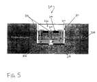
- FIG. 5illustrates a cross-sectional view of a flexible smart card, such as a credit card which includes integrated circuits and a display device, as in a display module, all on the same credit card substrate.
- a flexible smart cardsuch as a credit card which includes integrated circuits and a display device, as in a display module, all on the same credit card substrate.
- the present inventionpertains to methods for forming backside electrical contacts in flexible displays or RF tags using, in one embodiment, laser drilling.
- the present inventionalso pertains to apparatuses such as flexible displays or RF tags having backside electrical contacts.
- a metal backingcan be used to improve dimensional stability of the plastic substrate throughout the display manufacturing process.
- an adhesive layeris used to bond the metal backing to the plastic substrate.
- Dimensional stabilityis useful when the display manufacturing processes uses a roll to roll web process (which is similar to the manner in which paper is often fabricated).
- This metal backinghas in the past not been segmented in order to provide electrical contacts.
- this metal backing or other conductive backingis segmented into one or more electrodes.
- laser drillingis used to form through holes with sloped side walls into the plastic display substrate and/or to remove the adhesive layer bonding the metal backing to the plastic display substrate in cases where the through holes themselves are patterned into the plastic in a different manner.
- a preferred embodimentuses laser drilling to both form the through holes as well as to remove the adhesive layer which bonds the metal backing to the plastic display substrate or an RF device.
- the use of laser drillingcan form through holes with high accuracy and at a high rate with highly reproducible hole size and side wall slope which depends on the substrate, the laser wavelengths, and the laser pulse energy.
- the through hole connectionscan be completed in numerous ways, including, but not limited to, metal evaporation, metal sputtering, electroplating or electro-less plating, screen printing of conductive epoxy, conducting polymers, etc.
- the present inventionmay be used with a variety of display technologies and display media, including liquid crystals, organic light emitting diodes (OLED), and a polymer light emitting diode (PLED).
- the metal backingcan be used as electrodes in up emitting active matrix OLED displays, as well as in up emitting or down emitting passive matrix displays to route large currents consumed by such a display.
- the metal backingwhich is typically tens of microns thick, provides, in one embodiment, dimensional stability during the display manufacturing process (effectively providing a structural support to a substrate which is being exposed to various processes (in a roll to roll web process) and would subsequently be patterned into one or more discrete electrodes.
- the metal backingis at least 10% of the entire thickness of the structure which includes the metal backing.
- Such thick metal electrodesallow the routing of large currents with negligible voltage drop.
- Laser hole drilling followed by a suitable via completion technique, such as metal sputtering or electroplatingto facilitate rapid formation of highly reproducible, short, low resistance, well-aligned connections to driver electronics in their immediate proximity.
- One application of the present inventionis in the fabrication of smart cards and similar devices where separately manufactured displays may need to be integrated into the card. Ruggedness provided by the metal backing can be maintained, largely, while at the same time using the metal backing to provide multiple electrodes.
- FIGS. 1A, 1B, 1 C, 1 D, and 1 Eshow cross-sectional views of an apparatus having a flexible substrate and backside electrical contacts which can be used for a flexible display.
- the substrate of FIG. 1Aincludes a flexible substrate 10 and a conductive layer 11 .
- the flexible substrate 10is a plastic layer and the conductive layer 11 is a metal backing of a display.
- the conductive layer 11is coupled to the flexible substrate 10 .
- the metal backingis typically applied to the plastic layer using an adhesive (not shown).
- a flexible substrate 10may be attached to a polymer conductive material which provides electrical conductivity, while the plastic is an insulator.
- the polymer conductive materialmay also provide dimensional stability.
- FIG. 1Bshows that electrical components, such as display drivers or other electrical components (e.g. integrated circuits in the form of shaped blocks have been deposited into regions or receptors created in the flexible substrate 10 , such as the integrated circuits described in co-pending U.S. patent application Ser. No. 09/671,659, filed Sep. 27, 2000).
- the electrical componentscan be (a) row electrodes for a display, (b) column electrodes for a display, (c) integrated circuits for a display or a radio frequency tag, (d) supply electrodes for display drivers, and (e) other electrical components for a display, radio frequency tag, or any other suitable electronic device.
- the flexible substrate 10has a top surface 10 T and a bottom surface 10 B.
- the electrical componentsare incorporated near the top surface 10 T.
- the electrical componentsare incorporated just immediately below the top surface 10 T and within the flexible substrate 10 .
- FIG. 1Billustrates that integrated circuits 15 A and 15 B have been deposited into the flexible substrate 10 .
- an electrode 14such as a bus electrode or other type of electrode, is also included in the flexible substrate 10 .
- electrode 14 as well as integrated circuits 15 A and 15 Bmay be any of a variety of different electrical devices, such as display drivers or circuits to provide radio frequency tags, etc.
- the circuits 15 A and 15 Bare display drivers for the backplane of a display device, such as a liquid crystal display device or an OLED display device.
- Laser drillingis used, in one embodiment, to drill a hole or opening through the flexible substrate 10 such that the hole or opening exposes the conductive layer (e.g., the metal backing). Holes 17 , 18 and 19 are drilled through the flexible substrate 10 to expose a portion of the conductive layer 11 as shown in FIG. 1C. In one example, the holes or the openings are cut or drilled through the flexible substrate 10 from the top surface 10 T to the bottom surface 10 B. Then a conductive material or element is applied into these holes to form electrical contacts to the conductive layer 11 and also to form electrical contacts to electrical components on the opposite side of the flexible substrate 10 . As shown in FIG.
- conductive element 17 Amakes an electrical contact to a portion of the conductive layer 11 while also making another electrical contact to electrode 14 .
- conductive element 18 Amakes an electrical contact to a portion of the conductive layer 11 and also to an electrical interconnection pad (not shown) on the integrated circuit 15 A.
- the conductive element 19 Amakes an electrical contact to a portion of the conductive layer 11 and also to an electrical interconnection pad (not shown) on the integrated circuit 15 B.
- Examples of a conductive elementinclude metals such as copper, gold, silver, tungsten, aluminum, and any other suitable metal alloys. These examples do not represent an exhaustive list of the conductive element or material.
- the conductive layer 11is segmented into at least two segments.
- the conductive layer 11is patterned using conventional methods to create a conductive layer 11 with a plurality of conductors. After segmenting the conductive layer 11 into at least two segments 11 A and 11 B, the structure shown in FIG. 1E is produced.
- the conductive layer 11now comprises a plurality of conductors or electrodes. In this case, the conductive layer 11 has been segmented to produce at least two electrodes 11 A and 11 B to provide the proper electrical conductivity to portions of the circuits on the opposite face of the flexible substrate 10 .
- FIGS. 1A, 1B, 1 C, 1 D, and 1 Erepresent a particular example of the present invention and that alternative examples may be envisioned.
- the flexible substrate 10may be replaced with another material which can provide similar flexibility for a flexible display.
- the conductive layer 11may be replaced with a conductive polymer or other non-metallic material to provide sufficient conductivity for the electrodes which are to be created from the conductive layer 11 and this conductive polymer may also provide dimensional stability.
- the particular sequence of process operations shown by FIGS. 1A, 1B, 1 C, 1 D, and 1 Emay be altered such that certain operations are performed in a different sequence than that shown in FIGS. 1A, 1B, 1 C, 1 D, and 1 E.
- the backplane fabrication processmay be completed after segmenting the metal conductive layer 11 .
- FIG. 2is a flowchart showing an exemplary method of the present invention.
- a conductive backingis applied to the back of a flexible display backplane.
- a flexible display substratesuch as a plastic material may be commercially obtained with the metal backing already applied to it.
- the display backplane structurewhich includes the electrical components such as display drivers and row and column electrodes, is created on or in the surface of the flexible substrate in order to create a display backplane which is flexible.
- openingsare created in the top surface of the flexible display backplane such as the openings 17 , 18 , and 19 as shown in FIG. 1C. These openings expose a surface of the conductive backing, also as shown in FIG. 1C.
- the openingsare filled with a conductive material to make electrical connections to the conducting backing.
- a conductive materialis shown as conductive material 17 A, 18 A and 19 A as shown in FIG. 1D.
- the conductive backingis patterned to form conductors on the back of the flexible display backplane.
- FIG. 1EAn example of this patterning is shown in which the metal backing has been segmented into two electrodes 11 A and 11 B.
- a pattern of conductorsis created on the top surface to interconnect the conductive material, which is disposed in the openings and on the top surface, to electrical display components on the top surface of the flexible display backplane.
- FIG. 1EAn example of these conductors on the top surface is shown in FIG. 1E where the portion of the conductive material on the top surface is electrically coupled to electrical contacts on components such as components 15 A and 15 B on the top surface of the substrate 10 .
- FIG. 2is one exemplary method and that alternatives, including alternative sequences, are possible according to the present invention. For example, operations 58 and 56 may be reversed in sequence.
- FIG. 3illustrates another exemplary embodiment of the present invention.
- Operation 75 of this methodcreates a pattern of conductors on the bottom surface of a flexible display backplane.
- a metal backingsuch as the metal backing 11
- These openingsexpose a surface of at least some of the conductors on the bottom of the flexible backplane.
- the openingsare filled with conductive material to make electrical connections to at least some of the conductors on the bottom of the flexible display backplane.
- a pattern of conductors on the top surfaceis created to interconnect the conductive material in the openings to various electrical display components on the top surface of the flexible display backplane.
- FIG. 4Aa metal backed flexible plastic substrate 101 is the starting material which is shown in FIG. 4A.
- Column and row driver circuitryis created in the top surface of this substrate.
- One manner of creating this circuitryis to fabricate in semiconductor wafers various column and row drivers and then to separate these drivers from the wafers and deposit each individual integrated circuit as a block into a receptor region of the substrate 101 .
- the process for depositionmay include the use of fluidic self-assembly to deposit the blocks into the receptor regions.
- FIG. 4Aa metal backed flexible plastic substrate 101 is the starting material which is shown in FIG. 4A.
- Column and row driver circuitryis created in the top surface of this substrate.
- One manner of creating this circuitryis to fabricate in semiconductor wafers various column and row drivers and then to separate these drivers from the wafers and deposit each individual integrated circuit as a block into a receptor region of the substrate 101 .
- the process for depositionmay include the use of fluidic self-assembly to deposit the
- FIGS. 4B, 4C, 4 D, and 4 Einclude a set of conductors, the row conductors 105 , which exist on a separate substrate but are shown in these figures nevertheless.
- the row driverswill be coupled to the row electrodes through conventional techniques for forming a vertical interconnection from a first substrate, such as the substrate 101 , to a cover substrate. It may be noted that this example pertains more to a liquid crystal type of a display cell in which a liquid crystal compound is injected or sandwiched between the substrate 101 having the column conductors 104 and the other substrate having the row conductors 105 .
- the row conductor drivers and the column conductor driverscan both be on the same substrate or each be on the corresponding substrate of the rows and column conductors that each controls.
- the process creating the display cellmay be modified accordingly for other type of display.
- a sequential processis used to create the display cell.
- a substrateis first provided then conventional methods are used to deposit a layer of ITO, which is anode, on the substrate.
- the ITOis then patterned to form the column conductors much like the column conductors 104 discussed above.
- a display mediumsuch as an OLED stack (having a hole transport layer, an electroluminescent material, and an electron transport layer) is then deposited on the ITO layer.
- the OLED stackcan be replaced with a PLED stack or other suitable display material to maker other type of display.
- a cathode layeris deposited and patterned to form row conductors much like the row conductors 105 .
- a cover substrate(flexible or not) is deposited over the cathode layer completing the display cell.
- through holesare patterned into the plastic substrate so that row and column electrodes can be created on the backside of the substrate.
- through holes 107 A, 107 B and 107 Care formed to make backside connections for the column drivers 102 A, 102 B, and 102 C.
- through holes 108 A, 108 B, and 108 Care formed in the substrate 101 in order to make electrical connections from the backside to the row drivers 103 A, 103 B, and 103 C.
- the through holesare filled with a conductive material to establish electrical connections to the metal backing as shown in FIG. 4D.
- conductive material 110 A, 110 B, and 110 Cfill through holes 107 A, 107 B, and 107 C.
- conductive material 109 A, 109 B and 109 Cfill the through holes 108 A, 108 B, and 108 C.
- the metal backingis patterned into discrete electrodes to create electrodes 111 and 112 . This patterning may be done before or after the creation of the through holes. It will be appreciated that the particular discrete electrodes used to create electrical connections on the backside to the drivers on the top side depend upon the particular circuit or display being fabricated. The particular pattern shown in FIG. 4E is a simplistic representation of two separate electrodes, and it will be appreciated that various other types of electrode patterns may be created as required by the electrical circuit which the display device requires.
- FIG. 5shows a cross-sectional view of a smart card 200 , which includes a display device or module 211 fabricated with backside electrodes 201 according to one embodiment of the present invention.
- a display medium 220is sandwiched between a counter electrode 202 and the driver electronics 204 on the plastic substrate 206 through which through holes 210 have been created.
- the plastic substrate 206forms the display module for the smart card in this embodiment.
- the display module 211is deposited into an opening 208 in the flexible smart card 200 as shown in FIG. 5.
- a preferred embodiment of the present inventionuses laser drilling to create openings in the substrate 206 for the through holes 210 to make electrical connections from the backside 212 of the substrate 206 to the top surface 214 of the substrate 206 .
- the backside electrodes 201make contact to smart card contact pads 216 included with the smart card 200 .
- the smart card contact pads 216enable the display device to interconnect to a master controller (not shown) typically present in a smart card.
- the master controllercontrols the information that will be displayed in the display device.
- Various different types of lasersmay be employed to make these through holes mentioned in this discussion.
- the wavelength of these lasersmay vary from ultraviolet to infrared.
- a transverse excitation atmospheric pressure pulsed CO 2 lasercan be used for plastic substrates.
- the holes typically in this embodimentwill be tapered.
- a YAG laser from ESILaser Microvia Drill, model no. 5200
- an excimer lasermay be employed.
- the frequencymay be doubled, tripled, or quadrupled to provide a near ultraviolet wavelength.
Landscapes
- Physics & Mathematics (AREA)
- Microelectronics & Electronic Packaging (AREA)
- Engineering & Computer Science (AREA)
- General Physics & Mathematics (AREA)
- Computer Hardware Design (AREA)
- Nonlinear Science (AREA)
- Condensed Matter Physics & Semiconductors (AREA)
- Power Engineering (AREA)
- Crystallography & Structural Chemistry (AREA)
- Optics & Photonics (AREA)
- Chemical & Material Sciences (AREA)
- Devices For Indicating Variable Information By Combining Individual Elements (AREA)
- Structure Of Printed Boards (AREA)
Abstract
Description
- This application is based on U.S. Provisional patent application No. 60/286,838 filed on Apr. 25, 2001 entitled “Contacts For Flexible Displays.” This application claims priority of the provisional application so mentioned.[0001]
- The fabrication of flexible displays, particularly flexible displays which are fabricated through a process which includes fluidic self-assembly, has relied upon the creation of electrical interconnections on a single side of the display device. Examples of such flexible display devices are shown in co-pending U.S. patent application Ser. No. 09/671,659, which was filed Sep. 27, 2000.[0002]
- The present invention pertains to methods and apparatuses for forming electrical contacts for flexible displays and for radio frequency (RF) tags. In one exemplary embodiment of the invention, a method for fabricating a flexible display device includes forming openings in a top surface of a flexible substrate which forms a part of a flexible display device, where the flexible substrate has a bottom surface which includes a conductive layer, and the openings expose at least a portion of the conductive layer. This method further includes filling the openings with a conductive material which makes electrical contact to at least a portion of the conductive layer, where the conductive material is also for making electrical contact to electrical display components on the top surface.[0003]
- In another exemplary embodiment, a method for fabricating a flexible display device includes forming openings in a top surface of a flexible substrate which forms a part of a flexible display device, where the flexible substrate has a plurality of conductors disposed below the top surface, and the openings expose at least a portion of the plurality of conductors. The method further includes filling the openings with a conductive material which makes electrical contact to at least a portion of the plurality of conductors, where the conductive material also is for making electrical contact to electrical display components on the top surface.[0004]
- The methods of the present invention may also be utilized in fabricating a radio frequency (RF) tag to produce radio frequency tags or portions thereof which have double-sided contacts on a substrate.[0005]
- The present invention is illustrated by way of example and not limitation in the figures of the accompanying drawings in which like references indicate similar elements.[0006]
- FIGS. 1A, 1B,[0007]1C,1D, and1E show cross-sectional views of a substrate during a fabrication process for creating a flexible display or a radio frequency tag.
- FIG. 2 shows an exemplary method according to one embodiment of the present invention.[0008]
- FIG. 3 shows another exemplary method according to an embodiment of the present invention.[0009]
- FIGS. 4A, 4B,[0010]4C,4D, and4E illustrate a particular fabrication process for constructing a passive matrix display on a flexible substrate to produce a flexible display according to one embodiment of the invention.
- FIG. 5 illustrates a cross-sectional view of a flexible smart card, such as a credit card which includes integrated circuits and a display device, as in a display module, all on the same credit card substrate.[0011]
- In the following description, numerous specific details such as specific materials, processing parameters, processing steps, etc., are set forth in order to provide a thorough understanding of the invention. One skilled in the art will recognize that these details need not be specifically adhered in order to practice the claimed invention. In other instances, well known processing steps, materials, etc., are not set forth in order not to obscure the invention[0012]
- The present invention pertains to methods for forming backside electrical contacts in flexible displays or RF tags using, in one embodiment, laser drilling. The present invention also pertains to apparatuses such as flexible displays or RF tags having backside electrical contacts. In the process of manufacturing a flexible display, such as a plastic display, a metal backing can be used to improve dimensional stability of the plastic substrate throughout the display manufacturing process. In one example, an adhesive layer is used to bond the metal backing to the plastic substrate. Dimensional stability is useful when the display manufacturing processes uses a roll to roll web process (which is similar to the manner in which paper is often fabricated). This metal backing has in the past not been segmented in order to provide electrical contacts. In the present invention, this metal backing or other conductive backing is segmented into one or more electrodes.[0013]
- In one embodiment of the present invention, laser drilling is used to form through holes with sloped side walls into the plastic display substrate and/or to remove the adhesive layer bonding the metal backing to the plastic display substrate in cases where the through holes themselves are patterned into the plastic in a different manner. A preferred embodiment uses laser drilling to both form the through holes as well as to remove the adhesive layer which bonds the metal backing to the plastic display substrate or an RF device.[0014]
- The use of laser drilling can form through holes with high accuracy and at a high rate with highly reproducible hole size and side wall slope which depends on the substrate, the laser wavelengths, and the laser pulse energy. The through hole connections can be completed in numerous ways, including, but not limited to, metal evaporation, metal sputtering, electroplating or electro-less plating, screen printing of conductive epoxy, conducting polymers, etc.[0015]
- The present invention may be used with a variety of display technologies and display media, including liquid crystals, organic light emitting diodes (OLED), and a polymer light emitting diode (PLED). In one embodiment, the metal backing can be used as electrodes in up emitting active matrix OLED displays, as well as in up emitting or down emitting passive matrix displays to route large currents consumed by such a display. The metal backing, which is typically tens of microns thick, provides, in one embodiment, dimensional stability during the display manufacturing process (effectively providing a structural support to a substrate which is being exposed to various processes (in a roll to roll web process) and would subsequently be patterned into one or more discrete electrodes. In one embodiment, the metal backing is at least 10% of the entire thickness of the structure which includes the metal backing. Such thick metal electrodes allow the routing of large currents with negligible voltage drop. Laser hole drilling followed by a suitable via completion technique, such as metal sputtering or electroplating to facilitate rapid formation of highly reproducible, short, low resistance, well-aligned connections to driver electronics in their immediate proximity.[0016]
- One application of the present invention is in the fabrication of smart cards and similar devices where separately manufactured displays may need to be integrated into the card. Ruggedness provided by the metal backing can be maintained, largely, while at the same time using the metal backing to provide multiple electrodes.[0017]
- FIGS. 1A, 1B,[0018]1C,1D, and1E show cross-sectional views of an apparatus having a flexible substrate and backside electrical contacts which can be used for a flexible display. The substrate of FIG. 1A includes a
flexible substrate 10 and aconductive layer 11. In one example, theflexible substrate 10 is a plastic layer and theconductive layer 11 is a metal backing of a display. Theconductive layer 11 is coupled to theflexible substrate 10. The metal backing is typically applied to the plastic layer using an adhesive (not shown). There are many commercially available plastic substrates which already include a metal backing which has been attached to the plastic substrate. In an alternative embodiment, aflexible substrate 10 may be attached to a polymer conductive material which provides electrical conductivity, while the plastic is an insulator. In this embodiment, the polymer conductive material may also provide dimensional stability. - FIG. 1B shows that electrical components, such as display drivers or other electrical components (e.g. integrated circuits in the form of shaped blocks have been deposited into regions or receptors created in the[0019]
flexible substrate 10, such as the integrated circuits described in co-pending U.S. patent application Ser. No. 09/671,659, filed Sep. 27, 2000). The electrical components can be (a) row electrodes for a display, (b) column electrodes for a display, (c) integrated circuits for a display or a radio frequency tag, (d) supply electrodes for display drivers, and (e) other electrical components for a display, radio frequency tag, or any other suitable electronic device. These integrated circuits may be deposited into theflexible substrate 10 through a fluidic self-assembly process or other processes. Theflexible substrate 10 has atop surface 10T and abottom surface 10B. In one example, the electrical components are incorporated near thetop surface 10T. In another example, the electrical components are incorporated just immediately below thetop surface 10T and within theflexible substrate 10. FIG. 1B illustrates thatintegrated circuits flexible substrate 10. Furthermore, another type of electrical component, anelectrode 14, such as a bus electrode or other type of electrode, is also included in theflexible substrate 10. It will be appreciated thatelectrode 14 as well asintegrated circuits circuits - Laser drilling is used, in one embodiment, to drill a hole or opening through the[0020]
flexible substrate 10 such that the hole or opening exposes the conductive layer (e.g., the metal backing).Holes flexible substrate 10 to expose a portion of theconductive layer 11 as shown in FIG. 1C. In one example, the holes or the openings are cut or drilled through theflexible substrate 10 from thetop surface 10T to thebottom surface 10B. Then a conductive material or element is applied into these holes to form electrical contacts to theconductive layer 11 and also to form electrical contacts to electrical components on the opposite side of theflexible substrate 10. As shown in FIG. 1D,conductive element 17A makes an electrical contact to a portion of theconductive layer 11 while also making another electrical contact toelectrode 14. Similarly,conductive element 18A makes an electrical contact to a portion of theconductive layer 11 and also to an electrical interconnection pad (not shown) on theintegrated circuit 15A. Similarly, theconductive element 19A makes an electrical contact to a portion of theconductive layer 11 and also to an electrical interconnection pad (not shown) on theintegrated circuit 15B. Examples of a conductive element include metals such as copper, gold, silver, tungsten, aluminum, and any other suitable metal alloys. These examples do not represent an exhaustive list of the conductive element or material. - In one exemplary embodiment, the[0021]
conductive layer 11 is segmented into at least two segments. In one example, theconductive layer 11 is patterned using conventional methods to create aconductive layer 11 with a plurality of conductors. After segmenting theconductive layer 11 into at least two segments11A and11B, the structure shown in FIG. 1E is produced. Theconductive layer 11 now comprises a plurality of conductors or electrodes. In this case, theconductive layer 11 has been segmented to produce at least two electrodes11A and11B to provide the proper electrical conductivity to portions of the circuits on the opposite face of theflexible substrate 10. - It will be appreciated that FIGS. 1A, 1B,[0022]1C,1D, and1E represent a particular example of the present invention and that alternative examples may be envisioned. For example, the
flexible substrate 10 may be replaced with another material which can provide similar flexibility for a flexible display. Further, theconductive layer 11 may be replaced with a conductive polymer or other non-metallic material to provide sufficient conductivity for the electrodes which are to be created from theconductive layer 11 and this conductive polymer may also provide dimensional stability. Further, the particular sequence of process operations shown by FIGS. 1A, 1B,1C,1D, and1E may be altered such that certain operations are performed in a different sequence than that shown in FIGS. 1A, 1B,1C,1D, and1E. For example, the backplane fabrication process may be completed after segmenting the metalconductive layer 11. - It will also be appreciated that this discussion applies to electronic devices other than a display (see example below). Thus, the embodiments discussed are not limited to only flexible display.[0023]
- FIG. 2 is a flowchart showing an exemplary method of the present invention. In[0024]
process operation 50, a conductive backing is applied to the back of a flexible display backplane. In many instances, a flexible display substrate such as a plastic material may be commercially obtained with the metal backing already applied to it. The display backplane structure, which includes the electrical components such as display drivers and row and column electrodes, is created on or in the surface of the flexible substrate in order to create a display backplane which is flexible. Then inoperation 52, openings are created in the top surface of the flexible display backplane such as theopenings operation 54, the openings are filled with a conductive material to make electrical connections to the conducting backing. An example of this conductive material is shown asconductive material operation 56, the conductive backing is patterned to form conductors on the back of the flexible display backplane. An example of this patterning is shown in FIG. 1E in which the metal backing has been segmented into two electrodes11A and11B. Then inoperation 58, a pattern of conductors is created on the top surface to interconnect the conductive material, which is disposed in the openings and on the top surface, to electrical display components on the top surface of the flexible display backplane. An example of these conductors on the top surface is shown in FIG. 1E where the portion of the conductive material on the top surface is electrically coupled to electrical contacts on components such ascomponents substrate 10. It will be understood that the method of FIG. 2 is one exemplary method and that alternatives, including alternative sequences, are possible according to the present invention. For example,operations - FIG. 3 illustrates another exemplary embodiment of the present invention.[0025]
Operation 75 of this method creates a pattern of conductors on the bottom surface of a flexible display backplane. In this instance, a metal backing such as themetal backing 11, is patterned to create a plurality of conductors on the bottom surface before openings are created inoperation 77. These openings expose a surface of at least some of the conductors on the bottom of the flexible backplane. Then inoperation 79, the openings are filled with conductive material to make electrical connections to at least some of the conductors on the bottom of the flexible display backplane. Then inoperation 81, a pattern of conductors on the top surface is created to interconnect the conductive material in the openings to various electrical display components on the top surface of the flexible display backplane. Again, various alternative sequences of the method shown in FIG. 3 will be envisioned by those in the art. - FIGS. 4A, 4B,[0026]4C,4D and4E will now be referred to while describing an embodiment of the invention in which a passive matrix display is created with backside electrode contacts on a flexible display substrate. In one example, a metal backed flexible
plastic substrate 101 is the starting material which is shown in FIG. 4A. Column and row driver circuitry is created in the top surface of this substrate. One manner of creating this circuitry is to fabricate in semiconductor wafers various column and row drivers and then to separate these drivers from the wafers and deposit each individual integrated circuit as a block into a receptor region of thesubstrate 101. The process for deposition may include the use of fluidic self-assembly to deposit the blocks into the receptor regions. The example shown in FIG. 4B shows threerow drivers substrate 101 and three column drivers102A,102B, and102C also deposited onto thesubstrate 101. A set ofcolumn conductors 104 may typically be formed on the top surface of thesubstrate 101 and another set of conductors, the row conductors105, will be formed on a separate substrate such as a cover substrate or a flexible cover substrate. Thus it will be appreciated that FIGS. 4B, 4C,4D, and4E include a set of conductors, the row conductors105, which exist on a separate substrate but are shown in these figures nevertheless. It will be appreciated that the row drivers will be coupled to the row electrodes through conventional techniques for forming a vertical interconnection from a first substrate, such as thesubstrate 101, to a cover substrate. It may be noted that this example pertains more to a liquid crystal type of a display cell in which a liquid crystal compound is injected or sandwiched between thesubstrate 101 having thecolumn conductors 104 and the other substrate having the row conductors105. The row conductor drivers and the column conductor drivers can both be on the same substrate or each be on the corresponding substrate of the rows and column conductors that each controls. - The process creating the display cell may be modified accordingly for other type of display. For example, for an OLED or PLED, a sequential process is used to create the display cell. A substrate is first provided then conventional methods are used to deposit a layer of ITO, which is anode, on the substrate. The ITO is then patterned to form the column conductors much like the[0027]
column conductors 104 discussed above. A display medium such as an OLED stack (having a hole transport layer, an electroluminescent material, and an electron transport layer) is then deposited on the ITO layer. The OLED stack can be replaced with a PLED stack or other suitable display material to maker other type of display. Next, a cathode layer is deposited and patterned to form row conductors much like the row conductors105. A cover substrate (flexible or not) is deposited over the cathode layer completing the display cell. - As shown in FIG. 4C, through holes are patterned into the plastic substrate so that row and column electrodes can be created on the backside of the substrate. As shown in FIG. 4C, through[0028]
holes 107A,107B and107C are formed to make backside connections for the column drivers102A,102B, and102C. Similarly, throughholes 108A,108B, and108C are formed in thesubstrate 101 in order to make electrical connections from the backside to therow drivers conductive material 110A,110B, and110C fill throughholes 107A,107B, and107C. Similarly,conductive material 109A,109B and109C fill the throughholes 108A,108B, and108C. Then, as shown in FIG. 4E, the metal backing is patterned into discrete electrodes to create electrodes111 and112. This patterning may be done before or after the creation of the through holes. It will be appreciated that the particular discrete electrodes used to create electrical connections on the backside to the drivers on the top side depend upon the particular circuit or display being fabricated. The particular pattern shown in FIG. 4E is a simplistic representation of two separate electrodes, and it will be appreciated that various other types of electrode patterns may be created as required by the electrical circuit which the display device requires. - FIG. 5 shows a cross-sectional view of a smart card[0029]200, which includes a display device or
module 211 fabricated withbackside electrodes 201 according to one embodiment of the present invention. In this case, adisplay medium 220 is sandwiched between acounter electrode 202 and thedriver electronics 204 on the plastic substrate206 through which throughholes 210 have been created. The plastic substrate206 forms the display module for the smart card in this embodiment. Thedisplay module 211 is deposited into anopening 208 in the flexible smart card200 as shown in FIG. 5. - As noted above, a preferred embodiment of the present invention uses laser drilling to create openings in the substrate[0030]206 for the through
holes 210 to make electrical connections from the backside212 of the substrate206 to thetop surface 214 of the substrate206. Thebackside electrodes 201 make contact to smartcard contact pads 216 included with the smart card200. The smartcard contact pads 216 enable the display device to interconnect to a master controller (not shown) typically present in a smart card. The master controller controls the information that will be displayed in the display device. - Various different types of lasers may be employed to make these through holes mentioned in this discussion. The wavelength of these lasers may vary from ultraviolet to infrared. For plastic substrates, a transverse excitation atmospheric pressure pulsed CO[0031]2laser can be used. The holes typically in this embodiment will be tapered. In one embodiment, a YAG laser from ESI (Laser Microvia Drill, model no. 5200) may be employed. Alternatively, an excimer laser may be employed. In the case of the YAG laser, the frequency may be doubled, tripled, or quadrupled to provide a near ultraviolet wavelength.
Claims (43)
Priority Applications (8)
| Application Number | Priority Date | Filing Date | Title |
|---|---|---|---|
| US10/131,517US6864435B2 (en) | 2001-04-25 | 2002-04-23 | Electrical contacts for flexible displays |
| JP2004500334AJP2005524109A (en) | 2002-04-23 | 2003-04-22 | Electrical contacts for flexible displays |
| PCT/US2003/012540WO2003092073A2 (en) | 2002-04-23 | 2003-04-22 | Electrical contacts for flexible displays |
| EP03728493AEP1497865A2 (en) | 2002-04-23 | 2003-04-22 | Electrical contacts for flexible displays |
| KR10-2004-7017115AKR20040102168A (en) | 2002-04-23 | 2003-04-22 | Electrical contacts for flexible displays |
| AU2003234184AAU2003234184A1 (en) | 2002-04-23 | 2003-04-22 | Electrical contacts for flexible displays |
| CNB038093324ACN1322587C (en) | 2002-04-23 | 2003-04-22 | Flexible electronic device and manufacturing method thereof |
| US11/054,037US20050181641A1 (en) | 2002-04-23 | 2005-02-08 | Electrical contacts for flexible displays |
Applications Claiming Priority (2)
| Application Number | Priority Date | Filing Date | Title |
|---|---|---|---|
| US28683801P | 2001-04-25 | 2001-04-25 | |
| US10/131,517US6864435B2 (en) | 2001-04-25 | 2002-04-23 | Electrical contacts for flexible displays |
Related Child Applications (1)
| Application Number | Title | Priority Date | Filing Date |
|---|---|---|---|
| US11/054,037Continuation-In-PartUS20050181641A1 (en) | 2002-04-23 | 2005-02-08 | Electrical contacts for flexible displays |
Publications (2)
| Publication Number | Publication Date |
|---|---|
| US20030155151A1true US20030155151A1 (en) | 2003-08-21 |
| US6864435B2 US6864435B2 (en) | 2005-03-08 |
Family
ID=29268732
Family Applications (2)
| Application Number | Title | Priority Date | Filing Date |
|---|---|---|---|
| US10/131,517Expired - LifetimeUS6864435B2 (en) | 2001-04-25 | 2002-04-23 | Electrical contacts for flexible displays |
| US11/054,037AbandonedUS20050181641A1 (en) | 2002-04-23 | 2005-02-08 | Electrical contacts for flexible displays |
Family Applications After (1)
| Application Number | Title | Priority Date | Filing Date |
|---|---|---|---|
| US11/054,037AbandonedUS20050181641A1 (en) | 2002-04-23 | 2005-02-08 | Electrical contacts for flexible displays |
Country Status (7)
| Country | Link |
|---|---|
| US (2) | US6864435B2 (en) |
| EP (1) | EP1497865A2 (en) |
| JP (1) | JP2005524109A (en) |
| KR (1) | KR20040102168A (en) |
| CN (1) | CN1322587C (en) |
| AU (1) | AU2003234184A1 (en) |
| WO (1) | WO2003092073A2 (en) |
Cited By (19)
| Publication number | Priority date | Publication date | Assignee | Title |
|---|---|---|---|---|
| US20020088267A1 (en)* | 2000-10-27 | 2002-07-11 | Harald Beck | Method and device for controlling a setting element in a vehicle |
| US20050162606A1 (en)* | 2004-01-28 | 2005-07-28 | Doane J. W. | Liquid crystal display |
| US20050195354A1 (en)* | 2003-07-02 | 2005-09-08 | Doane Joseph W. | Single substrate liquid crystal display |
| US20060051517A1 (en)* | 2004-09-03 | 2006-03-09 | Eastman Kodak Company | Thermally controlled fluidic self-assembly method and support |
| US20060057293A1 (en)* | 2004-09-03 | 2006-03-16 | Eastman Kodak Company | Thermally controlled fluidic self-assembly |
| US20060202925A1 (en)* | 2004-12-07 | 2006-09-14 | William Manning | Remote cholesteric display |
| US20070063939A1 (en)* | 2005-09-16 | 2007-03-22 | Bellamy Alan K | Liquid crystal display on a printed circuit board |
| US20070139299A1 (en)* | 2003-07-02 | 2007-06-21 | Kent Display Incorporated | Stacked display with shared electrode addressing |
| US20070152928A1 (en)* | 2004-01-28 | 2007-07-05 | Kents Displays Incorporated | Drapable liquid crystal transfer display films |
| US7251882B2 (en) | 2004-09-03 | 2007-08-07 | Eastman Kodak Company | Method for assembling micro-components to binding sites |
| US20080085401A1 (en)* | 2006-10-04 | 2008-04-10 | Sean Matthew Garner | Electronic device and method of making |
| US20090121333A1 (en)* | 2006-11-30 | 2009-05-14 | Bruce Gardiner Aitken | Flexible substrates having a thin-film barrier |
| WO2009109183A1 (en)* | 2008-03-07 | 2009-09-11 | Osram Opto Semiconductors Gmbh | Optoelectronic component |
| US7687277B2 (en) | 2004-12-22 | 2010-03-30 | Eastman Kodak Company | Thermally controlled fluidic self-assembly |
| US7722929B2 (en) | 2005-08-18 | 2010-05-25 | Corning Incorporated | Sealing technique for decreasing the time it takes to hermetically seal a device and the resulting hermetically sealed device |
| US7829147B2 (en) | 2005-08-18 | 2010-11-09 | Corning Incorporated | Hermetically sealing a device without a heat treating step and the resulting hermetically sealed device |
| US8199086B2 (en) | 2004-01-28 | 2012-06-12 | Kent Displays Incorporated | Stacked color photodisplay |
| US9050622B2 (en) | 2005-08-18 | 2015-06-09 | Corning Incorporated | Method for inhibiting oxygen and moisture degradation of a device and the resulting device |
| US11532259B2 (en)* | 2015-09-25 | 2022-12-20 | Apple Inc. | Row driver configuration |
Families Citing this family (61)
| Publication number | Priority date | Publication date | Assignee | Title |
|---|---|---|---|---|
| JP4885541B2 (en)* | 2002-11-26 | 2012-02-29 | イー インク コーポレイション | Backplane and electro-optic display |
| WO2005073705A1 (en)* | 2004-01-29 | 2005-08-11 | Siemens Aktiengesellschaft | Electrochemical transducer array and the use thereof |
| US20080055581A1 (en)* | 2004-04-27 | 2008-03-06 | Rogers John A | Devices and methods for pattern generation by ink lithography |
| CN101427182B (en)* | 2004-04-27 | 2011-10-19 | 伊利诺伊大学评议会 | Composite patterning equipment for soft lithography |
| CN103646848B (en) | 2004-06-04 | 2018-06-05 | 伊利诺伊大学评议会 | The method of assembling printable semiconductor elements and manufacture electronic device |
| US8217381B2 (en)* | 2004-06-04 | 2012-07-10 | The Board Of Trustees Of The University Of Illinois | Controlled buckling structures in semiconductor interconnects and nanomembranes for stretchable electronics |
| US7521292B2 (en) | 2004-06-04 | 2009-04-21 | The Board Of Trustees Of The University Of Illinois | Stretchable form of single crystal silicon for high performance electronics on rubber substrates |
| US7799699B2 (en) | 2004-06-04 | 2010-09-21 | The Board Of Trustees Of The University Of Illinois | Printable semiconductor structures and related methods of making and assembling |
| US7943491B2 (en) | 2004-06-04 | 2011-05-17 | The Board Of Trustees Of The University Of Illinois | Pattern transfer printing by kinetic control of adhesion to an elastomeric stamp |
| AU2005322072A1 (en) | 2004-12-27 | 2006-07-06 | Quantum Paper, Inc. | Addressable and printable emissive display |
| US7301458B2 (en)* | 2005-05-11 | 2007-11-27 | Alien Technology Corporation | Method and apparatus for testing RFID devices |
| US7329942B2 (en)* | 2005-05-18 | 2008-02-12 | Ching-Fu Tsou | Array-type modularized light-emitting diode structure and a method for packaging the structure |
| EP1991723A2 (en) | 2006-03-03 | 2008-11-19 | The Board Of Trustees Of The University Of Illinois | Methods of making spatially aligned nanotubes and nanotube arrays |
| KR100829392B1 (en)* | 2006-08-24 | 2008-05-13 | 동부일렉트로닉스 주식회사 | SOC and its manufacturing method |
| EP2104954B1 (en) | 2007-01-17 | 2022-03-16 | The Board of Trustees of the University of Illinois | Optical systems fabricated by printing-based assembly |
| US8852467B2 (en) | 2007-05-31 | 2014-10-07 | Nthdegree Technologies Worldwide Inc | Method of manufacturing a printable composition of a liquid or gel suspension of diodes |
| US8877101B2 (en) | 2007-05-31 | 2014-11-04 | Nthdegree Technologies Worldwide Inc | Method of manufacturing a light emitting, power generating or other electronic apparatus |
| US8133768B2 (en)* | 2007-05-31 | 2012-03-13 | Nthdegree Technologies Worldwide Inc | Method of manufacturing a light emitting, photovoltaic or other electronic apparatus and system |
| US8846457B2 (en) | 2007-05-31 | 2014-09-30 | Nthdegree Technologies Worldwide Inc | Printable composition of a liquid or gel suspension of diodes |
| US9343593B2 (en) | 2007-05-31 | 2016-05-17 | Nthdegree Technologies Worldwide Inc | Printable composition of a liquid or gel suspension of diodes |
| US8384630B2 (en) | 2007-05-31 | 2013-02-26 | Nthdegree Technologies Worldwide Inc | Light emitting, photovoltaic or other electronic apparatus and system |
| US9534772B2 (en) | 2007-05-31 | 2017-01-03 | Nthdegree Technologies Worldwide Inc | Apparatus with light emitting diodes |
| US9018833B2 (en) | 2007-05-31 | 2015-04-28 | Nthdegree Technologies Worldwide Inc | Apparatus with light emitting or absorbing diodes |
| US8889216B2 (en) | 2007-05-31 | 2014-11-18 | Nthdegree Technologies Worldwide Inc | Method of manufacturing addressable and static electronic displays |
| US9425357B2 (en) | 2007-05-31 | 2016-08-23 | Nthdegree Technologies Worldwide Inc. | Diode for a printable composition |
| US8415879B2 (en) | 2007-05-31 | 2013-04-09 | Nthdegree Technologies Worldwide Inc | Diode for a printable composition |
| US9419179B2 (en) | 2007-05-31 | 2016-08-16 | Nthdegree Technologies Worldwide Inc | Diode for a printable composition |
| US8809126B2 (en) | 2007-05-31 | 2014-08-19 | Nthdegree Technologies Worldwide Inc | Printable composition of a liquid or gel suspension of diodes |
| US8674593B2 (en) | 2007-05-31 | 2014-03-18 | Nthdegree Technologies Worldwide Inc | Diode for a printable composition |
| KR100974816B1 (en)* | 2008-02-27 | 2010-08-10 | 주식회사 비즈모델라인 | Method and system for embedding RFID tag in electronic parts and recording medium |
| TWI723953B (en) | 2008-03-05 | 2021-04-11 | 美國伊利諾大學理事會 | Stretchable and foldable electronic devices |
| US8470701B2 (en)* | 2008-04-03 | 2013-06-25 | Advanced Diamond Technologies, Inc. | Printable, flexible and stretchable diamond for thermal management |
| US7992332B2 (en) | 2008-05-13 | 2011-08-09 | Nthdegree Technologies Worldwide Inc. | Apparatuses for providing power for illumination of a display object |
| US8127477B2 (en) | 2008-05-13 | 2012-03-06 | Nthdegree Technologies Worldwide Inc | Illuminating display systems |
| US8946683B2 (en)* | 2008-06-16 | 2015-02-03 | The Board Of Trustees Of The University Of Illinois | Medium scale carbon nanotube thin film integrated circuits on flexible plastic substrates |
| US8389862B2 (en) | 2008-10-07 | 2013-03-05 | Mc10, Inc. | Extremely stretchable electronics |
| JP5646492B2 (en)* | 2008-10-07 | 2014-12-24 | エムシー10 インコーポレイテッドMc10,Inc. | Stretchable integrated circuit and device with sensor array |
| US8372726B2 (en)* | 2008-10-07 | 2013-02-12 | Mc10, Inc. | Methods and applications of non-planar imaging arrays |
| US8097926B2 (en) | 2008-10-07 | 2012-01-17 | Mc10, Inc. | Systems, methods, and devices having stretchable integrated circuitry for sensing and delivering therapy |
| US8886334B2 (en)* | 2008-10-07 | 2014-11-11 | Mc10, Inc. | Systems, methods, and devices using stretchable or flexible electronics for medical applications |
| US8049327B2 (en)* | 2009-01-05 | 2011-11-01 | Taiwan Semiconductor Manufacturing Company, Ltd. | Through-silicon via with scalloped sidewalls |
| EP2430652B1 (en) | 2009-05-12 | 2019-11-20 | The Board of Trustees of the University of Illionis | Printed assemblies of ultrathin, microscale inorganic light emitting diodes for deformable and semitransparent displays |
| WO2011041727A1 (en) | 2009-10-01 | 2011-04-07 | Mc10, Inc. | Protective cases with integrated electronics |
| US20110218756A1 (en)* | 2009-10-01 | 2011-09-08 | Mc10, Inc. | Methods and apparatus for conformal sensing of force and/or acceleration at a person's head |
| US10441185B2 (en) | 2009-12-16 | 2019-10-15 | The Board Of Trustees Of The University Of Illinois | Flexible and stretchable electronic systems for epidermal electronics |
| US10918298B2 (en) | 2009-12-16 | 2021-02-16 | The Board Of Trustees Of The University Of Illinois | High-speed, high-resolution electrophysiology in-vivo using conformal electronics |
| US9936574B2 (en) | 2009-12-16 | 2018-04-03 | The Board Of Trustees Of The University Of Illinois | Waterproof stretchable optoelectronics |
| EP2547258B1 (en) | 2010-03-17 | 2015-08-05 | The Board of Trustees of the University of Illionis | Implantable biomedical devices on bioresorbable substrates |
| US9442285B2 (en) | 2011-01-14 | 2016-09-13 | The Board Of Trustees Of The University Of Illinois | Optical component array having adjustable curvature |
| US9765934B2 (en) | 2011-05-16 | 2017-09-19 | The Board Of Trustees Of The University Of Illinois | Thermally managed LED arrays assembled by printing |
| JP2014523633A (en) | 2011-05-27 | 2014-09-11 | エムシー10 インコーポレイテッド | Electronic, optical and / or mechanical devices and systems and methods of manufacturing these devices and systems |
| WO2012167096A2 (en) | 2011-06-03 | 2012-12-06 | The Board Of Trustees Of The University Of Illinois | Conformable actively multiplexed high-density surface electrode array for brain interfacing |
| KR101979354B1 (en) | 2011-12-01 | 2019-08-29 | 더 보오드 오브 트러스티스 오브 더 유니버시티 오브 일리노이즈 | Transient devices designed to undergo programmable transformations |
| JP2015521303A (en) | 2012-03-30 | 2015-07-27 | ザ ボード オブ トラスティーズ オブ ザ ユニヴァーシ | An electronic device that can be attached to the surface and can be attached to an accessory |
| US9171794B2 (en) | 2012-10-09 | 2015-10-27 | Mc10, Inc. | Embedding thin chips in polymer |
| US9075199B2 (en) | 2012-10-30 | 2015-07-07 | Apple Inc. | Displays with polarizer layers for electronic devices |
| AU2016270807A1 (en) | 2015-06-01 | 2017-12-14 | The Board Of Trustees Of The University Of Illinois | Miniaturized electronic systems with wireless power and near-field communication capabilities |
| MX2017015587A (en) | 2015-06-01 | 2018-08-23 | Univ Illinois | Alternative approach to uv sensing. |
| US10925543B2 (en) | 2015-11-11 | 2021-02-23 | The Board Of Trustees Of The University Of Illinois | Bioresorbable silicon electronics for transient implants |
| DE102016112104A1 (en)* | 2016-07-01 | 2018-01-04 | Osram Opto Semiconductors Gmbh | MODULAR MODULE |
| CN108682305B (en) | 2018-05-21 | 2021-04-27 | 京东方科技集团股份有限公司 | Flexible substrate and preparation method thereof, and flexible display device |
Citations (5)
| Publication number | Priority date | Publication date | Assignee | Title |
|---|---|---|---|---|
| US5111278A (en)* | 1991-03-27 | 1992-05-05 | Eichelberger Charles W | Three-dimensional multichip module systems |
| US5545291A (en)* | 1993-12-17 | 1996-08-13 | The Regents Of The University Of California | Method for fabricating self-assembling microstructures |
| US5996897A (en)* | 1995-08-01 | 1999-12-07 | Austria Card Plastikkarten Und Ausweissysteme Gesellschaft M.B.H | Data carrier having a module including a component and having a coil, and method of manufacturing such a data carrier |
| US6642611B2 (en)* | 1998-03-26 | 2003-11-04 | Kabushiki Kaisha Toshiba | Storage apparatus, card type storage apparatus, and electronic apparatus |
| US6693384B1 (en)* | 2002-02-01 | 2004-02-17 | Alien Technology Corporation | Interconnect structure for electronic devices |
Family Cites Families (23)
| Publication number | Priority date | Publication date | Assignee | Title |
|---|---|---|---|---|
| US5065227A (en)* | 1990-06-04 | 1991-11-12 | International Business Machines Corporation | Integrated circuit packaging using flexible substrate |
| JP3246927B2 (en)* | 1991-09-17 | 2002-01-15 | 電気化学工業株式会社 | Flexible matrix circuit board and display board |
| FR2708170B1 (en)* | 1993-07-19 | 1995-09-08 | Innovation Dev Cie Gle | Electronic circuits with very high conductivity and great finesse, their manufacturing processes, and devices comprising them. |
| US5824186A (en)* | 1993-12-17 | 1998-10-20 | The Regents Of The University Of California | Method and apparatus for fabricating self-assembling microstructures |
| US5783360A (en)* | 1994-04-13 | 1998-07-21 | Flex Products, Inc. | Flexible optical medium with dielectric protective overcoat |
| JP2863094B2 (en)* | 1994-08-05 | 1999-03-03 | 矢崎総業株式会社 | Wiring board connection method |
| DE19527359A1 (en)* | 1995-07-26 | 1997-02-13 | Giesecke & Devrient Gmbh | Circuit unit and method for manufacturing a circuit unit |
| JP3387714B2 (en)* | 1995-12-11 | 2003-03-17 | キヤノン株式会社 | Electron source, its manufacturing apparatus, manufacturing method, and image forming apparatus |
| JP3900630B2 (en)* | 1997-12-03 | 2007-04-04 | 株式会社デンソー | Remote ID tag |
| JP2000105548A (en)* | 1998-07-31 | 2000-04-11 | Denso Corp | Electrode substrate for display panel and method of manufacturing the same |
| DE19840220A1 (en)* | 1998-09-03 | 2000-04-20 | Fraunhofer Ges Forschung | Transponder module and method for producing the same |
| DE19846237A1 (en)* | 1998-10-07 | 2000-04-13 | Fraunhofer Ges Forschung | Process for the production of a microtransponder |
| US6404643B1 (en)* | 1998-10-15 | 2002-06-11 | Amerasia International Technology, Inc. | Article having an embedded electronic device, and method of making same |
| JP2000132657A (en)* | 1998-10-28 | 2000-05-12 | Dainippon Printing Co Ltd | IC card and manufacturing method thereof |
| JP2000286549A (en) | 1999-03-24 | 2000-10-13 | Fujitsu Ltd | Method for manufacturing substrate with via connection |
| WO2001026180A1 (en) | 1999-10-04 | 2001-04-12 | Amerasia International Technology, Inc. | Tamper-resistant wireless article including an antenna |
| JP2001242476A (en)* | 2000-02-29 | 2001-09-07 | Seiko Epson Corp | Liquid crystal device, method of manufacturing the same, and electronic equipment |
| JP4444435B2 (en)* | 2000-03-06 | 2010-03-31 | ソニーケミカル&インフォメーションデバイス株式会社 | Printed wiring board and method for manufacturing printed wiring board |
| JP4489899B2 (en)* | 2000-03-08 | 2010-06-23 | イビデン株式会社 | Method for manufacturing double-sided circuit board for multilayer printed wiring board |
| JP2001313181A (en)* | 2000-05-01 | 2001-11-09 | Sony Corp | Display device and manufacturing method of the same |
| JP3597769B2 (en)* | 2000-09-18 | 2004-12-08 | シャープ株式会社 | Manufacturing method of electronic components |
| JP2002108252A (en)* | 2000-09-29 | 2002-04-10 | Sanyo Electric Co Ltd | Electro-luminescence display panel |
| WO2002067329A1 (en) | 2001-02-16 | 2002-08-29 | Ignis Innovation Inc. | Flexible display device |
- 2002
- 2002-04-23USUS10/131,517patent/US6864435B2/ennot_activeExpired - Lifetime
- 2003
- 2003-04-22WOPCT/US2003/012540patent/WO2003092073A2/enactiveApplication Filing
- 2003-04-22KRKR10-2004-7017115Apatent/KR20040102168A/ennot_activeWithdrawn
- 2003-04-22JPJP2004500334Apatent/JP2005524109A/enactivePending
- 2003-04-22EPEP03728493Apatent/EP1497865A2/ennot_activeCeased
- 2003-04-22AUAU2003234184Apatent/AU2003234184A1/ennot_activeAbandoned
- 2003-04-22CNCNB038093324Apatent/CN1322587C/ennot_activeExpired - Fee Related
- 2005
- 2005-02-08USUS11/054,037patent/US20050181641A1/ennot_activeAbandoned
Patent Citations (5)
| Publication number | Priority date | Publication date | Assignee | Title |
|---|---|---|---|---|
| US5111278A (en)* | 1991-03-27 | 1992-05-05 | Eichelberger Charles W | Three-dimensional multichip module systems |
| US5545291A (en)* | 1993-12-17 | 1996-08-13 | The Regents Of The University Of California | Method for fabricating self-assembling microstructures |
| US5996897A (en)* | 1995-08-01 | 1999-12-07 | Austria Card Plastikkarten Und Ausweissysteme Gesellschaft M.B.H | Data carrier having a module including a component and having a coil, and method of manufacturing such a data carrier |
| US6642611B2 (en)* | 1998-03-26 | 2003-11-04 | Kabushiki Kaisha Toshiba | Storage apparatus, card type storage apparatus, and electronic apparatus |
| US6693384B1 (en)* | 2002-02-01 | 2004-02-17 | Alien Technology Corporation | Interconnect structure for electronic devices |
Cited By (37)
| Publication number | Priority date | Publication date | Assignee | Title |
|---|---|---|---|---|
| US20020088267A1 (en)* | 2000-10-27 | 2002-07-11 | Harald Beck | Method and device for controlling a setting element in a vehicle |
| US7170481B2 (en) | 2003-07-02 | 2007-01-30 | Kent Displays Incorporated | Single substrate liquid crystal display |
| US20050195354A1 (en)* | 2003-07-02 | 2005-09-08 | Doane Joseph W. | Single substrate liquid crystal display |
| US7737928B2 (en) | 2003-07-02 | 2010-06-15 | Kent Displays Incorporated | Stacked display with shared electrode addressing |
| US7773064B2 (en) | 2003-07-02 | 2010-08-10 | Kent Displays Incorporated | Liquid crystal display films |
| US20070126674A1 (en)* | 2003-07-02 | 2007-06-07 | Kent Displays Incorporated | Liquid crystal display films |
| US20070139299A1 (en)* | 2003-07-02 | 2007-06-21 | Kent Display Incorporated | Stacked display with shared electrode addressing |
| US20050162606A1 (en)* | 2004-01-28 | 2005-07-28 | Doane J. W. | Liquid crystal display |
| US8199086B2 (en) | 2004-01-28 | 2012-06-12 | Kent Displays Incorporated | Stacked color photodisplay |
| US8329058B2 (en) | 2004-01-28 | 2012-12-11 | Kent Displays Incorporated | Chiral nematic photo displays |
| US7236151B2 (en) | 2004-01-28 | 2007-06-26 | Kent Displays Incorporated | Liquid crystal display |
| US20070152928A1 (en)* | 2004-01-28 | 2007-07-05 | Kents Displays Incorporated | Drapable liquid crystal transfer display films |
| US7796103B2 (en) | 2004-01-28 | 2010-09-14 | Kent Displays Incorporated | Drapable liquid crystal transfer display films |
| US20070237906A1 (en)* | 2004-01-28 | 2007-10-11 | Kent Displays Incorporated | Chiral nematic photo displays |
| US20060057293A1 (en)* | 2004-09-03 | 2006-03-16 | Eastman Kodak Company | Thermally controlled fluidic self-assembly |
| US7251882B2 (en) | 2004-09-03 | 2007-08-07 | Eastman Kodak Company | Method for assembling micro-components to binding sites |
| US7629026B2 (en) | 2004-09-03 | 2009-12-08 | Eastman Kodak Company | Thermally controlled fluidic self-assembly |
| US20060051517A1 (en)* | 2004-09-03 | 2006-03-09 | Eastman Kodak Company | Thermally controlled fluidic self-assembly method and support |
| US20060202925A1 (en)* | 2004-12-07 | 2006-09-14 | William Manning | Remote cholesteric display |
| US7687277B2 (en) | 2004-12-22 | 2010-03-30 | Eastman Kodak Company | Thermally controlled fluidic self-assembly |
| US20100122654A1 (en)* | 2004-12-22 | 2010-05-20 | Ravi Sharma | Thermally controlled fluidic self-assembly |
| US8304990B2 (en) | 2005-08-18 | 2012-11-06 | Corning Incorporated | Hermetically sealing a device without a heat treating step and the resulting hermetically sealed device |
| US9050622B2 (en) | 2005-08-18 | 2015-06-09 | Corning Incorporated | Method for inhibiting oxygen and moisture degradation of a device and the resulting device |
| US8435604B2 (en) | 2005-08-18 | 2013-05-07 | Corning Incorporated | Sealing technique for decreasing the time it takes to hermetically seal a device and the resulting hermetically sealed device |
| US7829147B2 (en) | 2005-08-18 | 2010-11-09 | Corning Incorporated | Hermetically sealing a device without a heat treating step and the resulting hermetically sealed device |
| US7722929B2 (en) | 2005-08-18 | 2010-05-25 | Corning Incorporated | Sealing technique for decreasing the time it takes to hermetically seal a device and the resulting hermetically sealed device |
| US20070063939A1 (en)* | 2005-09-16 | 2007-03-22 | Bellamy Alan K | Liquid crystal display on a printed circuit board |
| US20080085401A1 (en)* | 2006-10-04 | 2008-04-10 | Sean Matthew Garner | Electronic device and method of making |
| US8017220B2 (en) | 2006-10-04 | 2011-09-13 | Corning Incorporated | Electronic device and method of making |
| US8927053B2 (en) | 2006-10-04 | 2015-01-06 | Corning Incorporated | Electronic device and method of making |
| US20090121333A1 (en)* | 2006-11-30 | 2009-05-14 | Bruce Gardiner Aitken | Flexible substrates having a thin-film barrier |
| US8435605B2 (en) | 2006-11-30 | 2013-05-07 | Corning Incorporated | Flexible substrates having a thin-film barrier |
| US8653509B2 (en) | 2008-03-07 | 2014-02-18 | Osram Opto Semiconductors Gmbh | Optoelectronic component |
| WO2009109183A1 (en)* | 2008-03-07 | 2009-09-11 | Osram Opto Semiconductors Gmbh | Optoelectronic component |
| DE102008013031B4 (en)* | 2008-03-07 | 2019-07-25 | Osram Oled Gmbh | Optoelectronic component |
| US11532259B2 (en)* | 2015-09-25 | 2022-12-20 | Apple Inc. | Row driver configuration |
| US12142180B2 (en) | 2015-09-25 | 2024-11-12 | Apple Inc. | Row driver configuration |
Also Published As
| Publication number | Publication date |
|---|---|
| CN1659702A (en) | 2005-08-24 |
| WO2003092073A3 (en) | 2004-05-27 |
| JP2005524109A (en) | 2005-08-11 |
| WO2003092073A2 (en) | 2003-11-06 |
| KR20040102168A (en) | 2004-12-03 |
| US6864435B2 (en) | 2005-03-08 |
| CN1322587C (en) | 2007-06-20 |
| EP1497865A2 (en) | 2005-01-19 |
| AU2003234184A1 (en) | 2003-11-10 |
| US20050181641A1 (en) | 2005-08-18 |
Similar Documents
| Publication | Publication Date | Title |
|---|---|---|
| US6864435B2 (en) | Electrical contacts for flexible displays | |
| US6816380B2 (en) | Electronic devices with small functional elements supported on a carrier | |
| US7070851B2 (en) | Web process interconnect in electronic assemblies | |
| US7561221B2 (en) | Apparatuses and methods for forming assemblies | |
| US7046328B2 (en) | Apparatuses and methods for flexible displays | |
| US8872314B2 (en) | Method for producing a component and device comprising a component | |
| WO2019204207A1 (en) | Systems and methods for forming direct drive microled displays | |
| CN113327890A (en) | Manufacturing method of backboard, display panel and display device | |
| EP4472359A1 (en) | Wiring board | |
| JP2001024081A (en) | Conductive substrate and method of manufacturing the same | |
| CN113299604A (en) | Manufacturing method of backboard, display panel and display device | |
| JP4963538B2 (en) | Integrated circuit device | |
| CN118250902A (en) | Heat dissipation substrate and manufacturing method thereof | |
| CN116259545A (en) | Packaging method of chip and packaging piece | |
| JP2004119419A (en) | Process for forming interlayer connection structure, process for manufacturing electronic circuit device, interlayer connection structure and electronic circuit device |
Legal Events
| Date | Code | Title | Description |
|---|---|---|---|
| AS | Assignment | Owner name:ALIEN TECHNOLOGY, CALIFORNIA Free format text:ASSIGNMENT OF ASSIGNORS INTEREST;ASSIGNORS:HERMANNS, ANNO;EISENHARDT, RANDOLPH W.;GENGEL, GLENN W.;REEL/FRAME:012833/0004 Effective date:20020423 | |
| AS | Assignment | Owner name:ALIEN TECHNOLOGY, CALIFORNIA Free format text:ASSIGNMENT OF ASSIGNORS INTEREST;ASSIGNORS:HERMANNS, ANNO;EISENHARDT, RANDOLPH W.;GENGEL, GLENN W.;REEL/FRAME:013293/0776 Effective date:20020423 | |
| STCF | Information on status: patent grant | Free format text:PATENTED CASE | |
| CC | Certificate of correction | ||
| FPAY | Fee payment | Year of fee payment:4 | |
| REMI | Maintenance fee reminder mailed | ||
| AS | Assignment | Owner name:EAST WEST BANK, CALIFORNIA Free format text:SECURITY AGREEMENT;ASSIGNOR:ALIEN TECHNOLOGY CORPORATION;REEL/FRAME:022440/0755 Effective date:20070830 Owner name:EAST WEST BANK,CALIFORNIA Free format text:SECURITY AGREEMENT;ASSIGNOR:ALIEN TECHNOLOGY CORPORATION;REEL/FRAME:022440/0755 Effective date:20070830 | |
| FPAY | Fee payment | Year of fee payment:8 | |
| AS | Assignment | Owner name:ALIEN TECHNOLOGY, LLC, CALIFORNIA Free format text:CHANGE OF NAME;ASSIGNOR:ALIEN TECHNOLOGY CORPORATION;REEL/FRAME:033888/0976 Effective date:20140917 | |
| AS | Assignment | Owner name:ALIEN TECHNOLOGY, LLC, FORMERLY KNOWN AS ALIEN TEC Free format text:RELEASE BY SECURED PARTY;ASSIGNOR:EAST WEST BANK;REEL/FRAME:035122/0207 Effective date:20150303 Owner name:QUATROTEC, INC., DELAWARE Free format text:RELEASE BY SECURED PARTY;ASSIGNOR:EAST WEST BANK;REEL/FRAME:035122/0207 Effective date:20150303 | |
| AS | Assignment | Owner name:RUIZHANG TECHNOLOGY LIMITED COMPANY, CHINA Free format text:ASSIGNMENT OF ASSIGNORS INTEREST;ASSIGNOR:ALIEN TECHNOLOGY, LLC;REEL/FRAME:035258/0817 Effective date:20150306 | |
| FPAY | Fee payment | Year of fee payment:12 |