US20030150385A1 - Apparatus for fabrication of thin films - Google Patents
Apparatus for fabrication of thin filmsDownload PDFInfo
- Publication number
- US20030150385A1 US20030150385A1US10/383,291US38329103AUS2003150385A1US 20030150385 A1US20030150385 A1US 20030150385A1US 38329103 AUS38329103 AUS 38329103AUS 2003150385 A1US2003150385 A1US 2003150385A1
- Authority
- US
- United States
- Prior art keywords
- substrate
- reaction chamber
- base part
- reaction
- movable part
- Prior art date
- Legal status (The legal status is an assumption and is not a legal conclusion. Google has not performed a legal analysis and makes no representation as to the accuracy of the status listed.)
- Granted
Links
Images


Classifications
- H—ELECTRICITY
- H01—ELECTRIC ELEMENTS
- H01L—SEMICONDUCTOR DEVICES NOT COVERED BY CLASS H10
- H01L21/00—Processes or apparatus adapted for the manufacture or treatment of semiconductor or solid state devices or of parts thereof
- H01L21/02—Manufacture or treatment of semiconductor devices or of parts thereof
- H01L21/04—Manufacture or treatment of semiconductor devices or of parts thereof the devices having potential barriers, e.g. a PN junction, depletion layer or carrier concentration layer
- H01L21/18—Manufacture or treatment of semiconductor devices or of parts thereof the devices having potential barriers, e.g. a PN junction, depletion layer or carrier concentration layer the devices having semiconductor bodies comprising elements of Group IV of the Periodic Table or AIIIBV compounds with or without impurities, e.g. doping materials
- H01L21/30—Treatment of semiconductor bodies using processes or apparatus not provided for in groups H01L21/20 - H01L21/26
- H01L21/31—Treatment of semiconductor bodies using processes or apparatus not provided for in groups H01L21/20 - H01L21/26 to form insulating layers thereon, e.g. for masking or by using photolithographic techniques; After treatment of these layers; Selection of materials for these layers
- C—CHEMISTRY; METALLURGY
- C23—COATING METALLIC MATERIAL; COATING MATERIAL WITH METALLIC MATERIAL; CHEMICAL SURFACE TREATMENT; DIFFUSION TREATMENT OF METALLIC MATERIAL; COATING BY VACUUM EVAPORATION, BY SPUTTERING, BY ION IMPLANTATION OR BY CHEMICAL VAPOUR DEPOSITION, IN GENERAL; INHIBITING CORROSION OF METALLIC MATERIAL OR INCRUSTATION IN GENERAL
- C23C—COATING METALLIC MATERIAL; COATING MATERIAL WITH METALLIC MATERIAL; SURFACE TREATMENT OF METALLIC MATERIAL BY DIFFUSION INTO THE SURFACE, BY CHEMICAL CONVERSION OR SUBSTITUTION; COATING BY VACUUM EVAPORATION, BY SPUTTERING, BY ION IMPLANTATION OR BY CHEMICAL VAPOUR DEPOSITION, IN GENERAL
- C23C16/00—Chemical coating by decomposition of gaseous compounds, without leaving reaction products of surface material in the coating, i.e. chemical vapour deposition [CVD] processes
- C23C16/44—Chemical coating by decomposition of gaseous compounds, without leaving reaction products of surface material in the coating, i.e. chemical vapour deposition [CVD] processes characterised by the method of coating
- C23C16/455—Chemical coating by decomposition of gaseous compounds, without leaving reaction products of surface material in the coating, i.e. chemical vapour deposition [CVD] processes characterised by the method of coating characterised by the method used for introducing gases into reaction chamber or for modifying gas flows in reaction chamber
- C23C16/45523—Pulsed gas flow or change of composition over time
- C23C16/45525—Atomic layer deposition [ALD]
- C23C16/45544—Atomic layer deposition [ALD] characterized by the apparatus
- C—CHEMISTRY; METALLURGY
- C30—CRYSTAL GROWTH
- C30B—SINGLE-CRYSTAL GROWTH; UNIDIRECTIONAL SOLIDIFICATION OF EUTECTIC MATERIAL OR UNIDIRECTIONAL DEMIXING OF EUTECTOID MATERIAL; REFINING BY ZONE-MELTING OF MATERIAL; PRODUCTION OF A HOMOGENEOUS POLYCRYSTALLINE MATERIAL WITH DEFINED STRUCTURE; SINGLE CRYSTALS OR HOMOGENEOUS POLYCRYSTALLINE MATERIAL WITH DEFINED STRUCTURE; AFTER-TREATMENT OF SINGLE CRYSTALS OR A HOMOGENEOUS POLYCRYSTALLINE MATERIAL WITH DEFINED STRUCTURE; APPARATUS THEREFOR
- C30B25/00—Single-crystal growth by chemical reaction of reactive gases, e.g. chemical vapour-deposition growth
- C30B25/02—Epitaxial-layer growth
- C30B25/08—Reaction chambers; Selection of materials therefor
- C—CHEMISTRY; METALLURGY
- C30—CRYSTAL GROWTH
- C30B—SINGLE-CRYSTAL GROWTH; UNIDIRECTIONAL SOLIDIFICATION OF EUTECTIC MATERIAL OR UNIDIRECTIONAL DEMIXING OF EUTECTOID MATERIAL; REFINING BY ZONE-MELTING OF MATERIAL; PRODUCTION OF A HOMOGENEOUS POLYCRYSTALLINE MATERIAL WITH DEFINED STRUCTURE; SINGLE CRYSTALS OR HOMOGENEOUS POLYCRYSTALLINE MATERIAL WITH DEFINED STRUCTURE; AFTER-TREATMENT OF SINGLE CRYSTALS OR A HOMOGENEOUS POLYCRYSTALLINE MATERIAL WITH DEFINED STRUCTURE; APPARATUS THEREFOR
- C30B25/00—Single-crystal growth by chemical reaction of reactive gases, e.g. chemical vapour-deposition growth
- C30B25/02—Epitaxial-layer growth
- C30B25/12—Substrate holders or susceptors
- C—CHEMISTRY; METALLURGY
- C30—CRYSTAL GROWTH
- C30B—SINGLE-CRYSTAL GROWTH; UNIDIRECTIONAL SOLIDIFICATION OF EUTECTIC MATERIAL OR UNIDIRECTIONAL DEMIXING OF EUTECTOID MATERIAL; REFINING BY ZONE-MELTING OF MATERIAL; PRODUCTION OF A HOMOGENEOUS POLYCRYSTALLINE MATERIAL WITH DEFINED STRUCTURE; SINGLE CRYSTALS OR HOMOGENEOUS POLYCRYSTALLINE MATERIAL WITH DEFINED STRUCTURE; AFTER-TREATMENT OF SINGLE CRYSTALS OR A HOMOGENEOUS POLYCRYSTALLINE MATERIAL WITH DEFINED STRUCTURE; APPARATUS THEREFOR
- C30B25/00—Single-crystal growth by chemical reaction of reactive gases, e.g. chemical vapour-deposition growth
- C30B25/02—Epitaxial-layer growth
- C30B25/16—Controlling or regulating
- C30B25/165—Controlling or regulating the flow of the reactive gases
Definitions
- the present inventionrelates to an apparatus according to the preamble of claim 1 for fabrication of thin-films.
- a substrate placed in a reaction spaceis subjected to alternate surface reactions of at least two different reactants suitable for fabricating a thin film.
- the vapor-phase reactantsare fed in a repetitive and alternating manner each at a time from its own supply into a reaction space, wherein they are brought to react with the surface of a substrate in order to produce a solid-state thin film product on the substrate. Reaction products not adhering to the substrate and possible excess reactants are removed in gas phase from the reaction space.
- the thin film growth rateis also affected by the concentrations of the starting material inflows.
- concentrations and reactivities of the starting materialsmust be kept equal on one side of the substrate. If the different starting materials are allowed to mix with each other prior to reaching the substrate surface as is the case in the CVD method, the possibility of mutual reactions between the reagents is always imminent. Herein arises a risk of microparticle formation already in the infeed lines of the gaseous reactants. Such microparticles generally have a deteriorating effect on the quality of the deposited thin film.
- the occurrence of premature reactions in MBE and CVD reactorscan be avoided, e.g., by heating the reactants not earlier than only at the substrates.
- the desired reactioncan be initiated with the help of, e.g., plasma or other similar activating means.
- the growth rate of thin-filmsis primarily adjusted by controlling the inflow rates of starting materials impinging on the substrate.
- the thin film growth rate in the ALE processis controlled by the substrate surface properties, rather than by the concentrations or other qualities of the starting material inflows.
- the only prerequisiteis that the starting material is provided in a sufficient concentration for film growth on the substrate.
- the ALE methodis described, e.g., in Fl Patents Nos. 52,359 and 57,975 as well as in U.S. Pat. Nos. 4,058,430 and 4,389,973. Also in FI Patents Nos. 97,730, 97,731 and 100,409 are disclosed some apparatus constructions suited for implementing the method. Equipment for thin film deposition are further described in publications Material Science Report 4(7), 1989, p. 261, and Tyhjiotekniikka (title in English: Vacuum Techniques), ISBN 951-794-422-5 , pp. 253-261 .
- the saturation stepis followed by a protective gas pulse forming a diffusion barrier that sweeps away the excess starting material and the gaseous reaction products from the substrate.
- the successive pulses of different starting materials and the protective gas pulses forming diffusion barriers that separate the successive starting materials pulses from each otheraccomplish the growth of the thin film at a rate controlled by the surface chemistry properties of the different materials. To the function of the process it is irrelevant whether they are the gases or the substrates that are kept in motion, but rather, it is imperative that the different starting materials of the successive reaction steps are separated from each other and arranged to impinge on the substrate alternately.
- the “multi-shot” type ALE reactorsare provided with a reactor chamber structure comprised of a plurality of adjacently or superimposedly stacked modular elements of which at least some are identical to each other and by milling, for instance, have reaction chambers made thereto with suitable cutouts and openings serving as the inlet and outlet channels.
- the substratescan be placed in an exposed manner in the interior of the vacuum vessel acting as the reaction space. In both arrangements, the reactor must be pressurized in conjunction with the substrate load/unload step.
- the reactorsare preferably run under constant process conditions stabilized in respect to the process temperature, operating pressure as well as for other process parameters.
- the goal hereinis to prevent the attack of foreign particles and chemical impurities from the environment on the substrates and to avoid thermal cycling of the reactors that is a time-consuming step and may deteriorate the process reliability.
- these problemsare overcome by using a separate substrate load/transfer chamber.
- the substrate loading chambercommunicates with the reactors and is kept under a constant vacuum.
- the load and unload steps of the substratesare performed so that both the reactor and the loading chamber are taken to a vacuum, after which the valve (such as a gate valve) separating the two from each other is opened, whereby a robotic arm constructed into the loading chamber removes a processed substrate from the reaction chamber and loads a new substrate. Subsequently, the valve is closed and the process may start after the substrate and the reactor have attained their nominal process values. On the other side, the processed substrate is transferred via another controllable valve from the loading chamber to a vacuumized load lock, after which the load lock valve is closed. Next, the load lock may be pressurized, after which the substrate can be removed from the equipment via a third valve opening into the room space. Respectively, the next substrate to be processed can be transferred via the loading chamber into the reactor.
- the valvesuch as a gate valve
- the substrateis placed on a heater so that the robotic arm can move the substrate to a desired point in the interior of the reactor, after which the substrate is elevated typically with the help of three pins directly upward for the duration of the robotic arm withdrawal.
- the substrateis lowered onto a heatable susceptor platform by lowering said pins below the surface level of said susceptor, whereby the substrate remains resting in a good thermal contact with the susceptor.
- the gas flowenters the reaction space via a “shower head” located above the substrate so as to distribute the gas over the hot substrate, whereby the desired surface reaction can take place and form a desired type of thin-film layer on the substrate surface.
- this type of infeed techniquewould require that, at the beginning and end of each reactant infeed pulse, a period of a duration generally equally to that of the reactant pulse length would become indispensable in order to allow for the homogenization of the gas concentration and flush-out of the previous gas pulse. In practice, this would lead to the mixing of the reactant vapors with each other, whereby the ALCVD mode of film growth would actually turn into a CVD process.
- the processis hampered by a slow throughput, poor material utilization efficiency and/or large thickness variations.
- the ALE methodalso can be utilized for depositing composite layer structures, whereby a single run can be employed for making a plurality of different film structures in a single batch. Thus, also the processing time per fabricated unit can be reduced.
- the large stack assemblies required in batch processesare typically put together in some auxiliary space, after which they must be transferred as compact units into the interior of the opened reactor.
- the bake-out heating of the reactor chamber structurestakes a few hours (1-4 h) followed by the processing step (taking about 2-4 h to a thickness of 300 nm Al 2 O 3 ), and the cooling lasts up to tens of hours depending on the size of the reactor construction.
- a certain timemust be counted for the dismantling and reassembly of the reactor chamber.
- the goal of the inventionis achieved by virtue of a novel concept in which the benefits of a reactor chamber structure and those of a cold-wall ALE reactor are combined with those of reactor equipped with an internal loading chamber through designing reaction chamber construction such that can be opened and closed in the interior of the reactor for the substrate load/unload steps.
- the reactor volumeis so small that there is not enough space for wafer handling. Therefore, the reaction chamber needs to be opened, not by a valve but by taking parts of the reactor apart, for wafer transfer.
- a second chamberis built around the reaction chamber.
- the reaction chamber constructioncomprises at least one part movable with respect to the remaining part of the reaction chamber and adapted to be sealably closable against said remaining part of the reaction chamber such that a substrate can be loaded / unloaded into and out of the reaction chamber.
- the reactor chambercomprises at least two basic parts, namely a stationary base part of the reactor structure and a movable part of said structure, the latter being adapted to be sealably closable against said base part, whereby the reaction space remaining between said base part and said movable part attains the characteristic shape required from such a volume.
- One combination element formed by the base part and the movable part of the reaction chamber structureacts as a substrate support platform, or base, on which a substrate can be positioned by means of a robotic arm or by the movements of a given part of said arm.
- the basic ideais to have reactor chamber parts which are movable with respect to each other, e.g. one horizontally, the other vertically, or both vertically.
- the apparatus according to the inventionis principally characterized by what is stated in the characterizing part of claim 1.
- the inventionoffers significant benefits. Accordingly, the construction according to the invention counteracts to the contamination of the intermediary spaces of the reactor, whereby also the cleanliness of the loading chamber is improved, the contamination risk of substrates reduced and the base pressure can be pumped down at a faster rate.
- the commercial processing of single substrates facilitated by the apparatus according to the inventionoffers the further benefit that each substrate can be processed in a tailored manner if so desired.
- the ALE processneed not anymore be run in a batch mode if the other production units are operated in a continuous mode.
- the apparatus according to the inventionis also applicable to the fabrication of different types of thin films including those of the semiconductor variety, as well as thin-film structures of display units by means of the ALE method.
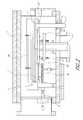
- FIG. 1shows a top view of an assembly diagram for a simplified construction of a reactor embodiment according to the invention:
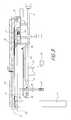
- FIG. 2shows a side view of the a simplified construction of the reactor embodiment
- FIG. 3shows longitudinally sectional side view of the simplified construction of the reactor embodiment.
- the term “reactant”refers to a vaporizable material capable of reacting with the substrate surface.
- the reactantsmay be solids, liquids or gases.
- reactants belonging to two different groupsare conventionally employed.
- the term “metallic reactants”is used of metallic compounds or even elemental metals. Suitable metallic reactants are the halogenides of metals including chlorides and bromides, for instance, and metalorganic compounds such as the thd complex compounds.
- metallic reactants Zn, ZnCl 9 , TiCl 4 , Ca(thd) 2 , (CH 3 ) 3 Al and Cp 2 ,Mgmay be mentioned.
- nonmetallic reactantsrefers to compounds and elements capable of reacting with metallic compounds. The latter group is typically represented by water, sulfur, hydrogen sulfide and ammonia.
- the term “protective gas” gasis used to refer to a gas which is admitted into the reaction space and is capable of preventing undesired reactions related to the reactants and, correspondingly, the substrate. Such reactions include e.g. the reactions of the reactants and the substrate with possible imnpurities.
- the protective gasalso serves to prevent reactions between substances of different reactant groups in, e.g., the inflow lines.
- the protective gasis also advantageously used as the carrier gas of the vapor-phase pulses of the reactants.
- the vapor-phase reactant pulseis admitted from one inflow channel while the protective gas is admitted from another inflow channel thus preventing the admitted reactant from entering an inflow channel serving another reactant group.
- protective gasessuited for use in the method, reference is made to inert gases such as nitrogen gas and noble gases, e.g., argon.
- the protective gasmay also be an inherently reactive gas such as hydrogen gas serving to prevent undesirable reactions (e.g., oxidization reactions) from occurring on the substrate surface.
- reaction spaceincludes both that part of the reaction chamber in which the substrate is located and in which the vapor-phase reactants are allowed to react with the substrate in order to grow thin films as well as the gas inflow/outflow channels communicating immediately with the reaction chamber, said channels serving for admitting the reactants into the reaction chamber (via inflow channels) or removing the gaseous reaction products of the thin-film growth process and excess reactants from the reaction chamber (via outflow channels).
- the number of the inflow and outflow channels, respectivelycan be varied from one upward.
- each reactant groupmay also be located at opposite ends of the substrates whereby the outflow orifice corresponding to each reactant group is located at the end of the inflow manifold of the other group, advantageously separated therefrom by means of a gas separating plate.
- the gasesmay also be fed onto the substrate alternately from opposite directions. In this manner it is possible to compensate any observed stronger film growth at the inflow end of the substrate. Also the exhaust suction from the outflow channel in such an arrangement must take place in an alternated manner.
- the gas feed inlet openingscan be arranged along a curved line, e.g. along a line having a radius of curvature somewhat greater than the radius of the circular substrate to be treated. By means of this arrangement it is possible to obtain an even gas front long the substrate.
- substrate surfaceis used to denote that top surface of the substrate onto which the vapor-phase reactant flowing into the reaction chamber primarily impinges.
- said surface, during the first cycle of the thin-film growing processis constituted by the surface of the substrate such as glass or silicon wafer, for instance; during the second cycle the surface is constituted by the layer formed during the first cycle and comprising the solid-state reaction product which is deposited by the reaction between the reactants and is adhered to the substrate, etc.
- the reactor chamberis fitted within an air- and gas-tight containment, such as a vacuum vessel.
- a reaction chambercomprises e.g. at least two parts, at least one of which is movable with respect to the remaining part of the reaction chamber and adapted to be sealably closable against said remaining part of the reaction chamber such that a substrate can be loaded and unloaded into and our of the reaction chamber.
- the partscan be moved with respect to each other (one or both); one horizontally (perpedicularly to the lateral plane of the substrate), the other vertically (laterally); or both vertically (laterally).
- the parts of the reaction chamberare contained in a second chamber, which preferably comprises a vacuum vessel, both during processing and during loading and unloading of a substrate.
- a second chamberwhich preferably comprises a vacuum vessel, both during processing and during loading and unloading of a substrate.
- the reaction chambercomprises two parts, one of which being mounted stationary in respect to said vacuum vessel, while the other is designed movable.
- the transfer of the movable partcan take place laterally, that is, parallel to the substrate plane, or alternatively, in a direction perpendicular to the plane of the stationary base part (and thus, to the plane of the substrate).
- the transfer motionmay also occur in both a lateral and a perpendicular direction.
- the substratecan be adapted mountable on the movable part or on the stationary base part or, in some cases, even on both parts.
- the stationary partis equipped with a rabbet encircling its edge, while the movable part is provided with an outer edge that is shaped conforming to the rabbet shape in order to provide a seal against the stationary base part.
- the reactor chamberis located in the manner disclosed in FI Patent No.97,730 in the interior of a cold-wall vacuum reactor.
- the term “cold-wall” reactoris used for making reference to an apparatus in which the reaction space and a possible reagent source adapted inside the vacuum vessel are heated each separately.
- the heating systemcan be implemented by enclosing each unit of the apparatus within a cover having one side facing the reactor (or source) equipped with a first temperature-equalizing jacket or plate and the other side facing the vacuum vessel wall possibly with another temperature-equalizing jacket or plate.
- a heating meanssuitable for heating the surfaces of said temperature equalizing jackets.
- a heating meansmay comprise tubular resistive elements or planar heaters.
- the envelopes of the covers enclosing the reaction space and the material sourcesare most advantageously made from a metal such as stainless steel, titanium or aluminum, or a suitable metal alloy or even a pure metal.
- the cold-wall vacuum vesselmay be replaced by some other type of gastight vessel. This is particularly true for a situation in which the reaction temperature is below about 200° C.
- the structure discussed hereinis called generally with the name “pressure-tight vessel” or “vacuum vessel”, said term also including so-called “vacuum vessels”. While the growth of a thin-film can be carried out under an atmospheric pressure or even a slight overpressure, operation under a partial vacuum will provide certain benefits in respect to the purity of reactant and purge gases, among other things.
- the base part of the reactor chamberis supported to the walls of the vacuum vessel so that the center axis of the support means is coincident with the center point of the substrate.
- This arrangementprevents mechanical deformations of thermal origin from affecting the extremely critical positioning of the substrate when the reactor chamber is being closed.
- the movable partcomprises a vertically movable plate transferred supported by a transport rod
- said rodis advantageously extended to the exterior of the vacuum vessel through the same wall as is penetrated by the gas channels.
- the transport rodcan be made movable by manual or actuator-driven means.
- the base partmay be made to comprise a portion of the vacuum vessel wall.
- the stationary base part of the reactor and/or its movable partis provided with heating means, whereby their insulation can be accomplished as needed by means of, e.g., reflective shields or active thermal insulation elements.
- heating meanse.g., reflective shields or active thermal insulation elements.
- reflective shields and active thermal insulation elementsreference is made to cited FI Patent No. 97,730.
- active thermal insulation elementstypically include a cooling means and a reflective shield.
- thermal radiation reflecting envelopesabout the heating means, whereby the number of the envelopes is at least one, but also a greater number of envelopes may be used in concentrically enclosing fashion.
- the sourcesare further surrounded by a cooling means, thus accomplishing the above-described cooled zone. This is necessary in the case that the sources are adapted to the interior of the vacuum vessel.
- the cooling systemmay be based on a water circulation, for instance.
- a similar cooling systemmay be constructed on the wall of the vacuum vessel, too.
- the sealing of the movable partcan be accomplished by means of, e.g., an elastomer seal if possible within the constraints of the process and the temperatures involved. Otherwise, the sealing must be made using, e.g., a vacuum pump-out groove seal construction.
- the sealing effect of the vacuum pump-out groovemay be augmented by feeding a protective gas into the groove.
- This type of vacuum pump-out groove sealcan be implemented by, e.g., machining on the surface of the planar structural elements of the chamber, close to the plate edges, a groove shaped as a loop passing close to the edge contour of the plate, thus being capable of sucking away any leaks.
- the vacuum pump-out grooveis connected to a discharge channel which is kept under a vacuum.
- the vacuum pump-out grooveserves to prevent the access of contamination from the exterior of the reactor into the reaction space or, conversely, the entering reactants from escaping to the exterior side of the reaction space.
- the sealing flow passing in the vacuum pump-out grooveprovides a maximally effective function if the heaviest constriction to the flow of gases is arranged in the vicinity of the trailing end of the substrate, close to the vacuum suction channel.
- edges of the opposedly mating parts of the reaction chamberare provided with notches cut at right angles to the plane of the plate so as to extend through the plate, thus forming the gas channels of the reaction space when the reaction chamber structure is fully closed.
- the reaction chambercan be shaped to accommodate a plurality of substrates. Accordingly, the reaction chamber may be provided with support structures on which at least two substrates can be placed for depositing thin-film structures on both substrates simultaneously.
- support structuresmay comprise a rack having platform shelves or brackets provided thereon for supporting the substrates, or alternatively, a cassette unit consisting of stackable, preferably mutually identical, modular elements, whereby the interior spaces of at least a part of the stackable elements are shaped so that they will be able to accomodate the substrates.
- these elementsare provided support brackets or platforms for the substrates.
- the support structuresmay be placed on the stationary base part of the reactor or, alternatively, on a movable base plate.
- the racksmay have either an open or a closed structure.
- an open rackthe sides are left open so as to give a free access for the reactant gases from the infeed channel to the substrates and, conversely, from the substrates to the discharge channel.
- a closed rackthe sides are partially closed, whereby the flow of the reactant gases takes place via infeed openings provided at one side of the rack, close to the substrates, while the other side is respectively equipped with a discharge opening.
- substrate holderscomprised of shelf platforms or brackets serving to support the substrates. The latter arrangement also facilitates two-sided deposition on the substrates. If the substrate support is provided by shelf platforms, they can be equipped with heating means serving to stabilize the reaction temperature.
- the reaction chambermay be composed of essentially similar (even identical) modular elements stacked on a base plate, whereby the proper design of the stack elements have indents and grooves made thereto such that narrow passageways are formed acting as flow constrictors to the gas flowing through the reaction space.
- the elementshave recesses made thereto with surfaces acting as substrate supports.
- the components of such a stackable cassette pack structureare fabricated from a material that is resistant to the reactants used in the ALE growth process.
- advantageous materialsare glass and the like silicate-based compositions, as well as various ceramics.
- the same groups of materials, as well as various metal alloys,are also suitable for making the racks.
- the internal surfaces of the process equipmentmay be passivated by depositing thereon, e.g., an Al 2 O 3 layer that can be formed using ALCVD from suitable starting materials such as aluminum chloride and water.
- the inlet and outlet lines (or feeding/pumping lines) of the reactant gasesare advantageously connected in a permanent manner to the reaction chamber.
- the substrate rack or cassette structureis advantageously arranged in the reaction chamber so that the end of the gas discharge channel meets the gas discharge opening of the rack or cassette structure as tightly as possible.
- the substratesmay also be arranged in an essentially upright position in the reaction space.
- the movable partis equipped with a substrate lift means, whose upright movement facilitates easy placement of the substrate onto the robotic arm.
- substrate lift meanscan comprise, e.g., pins inserted in holes made on the substrate support surface so as to force the pegs to move at right angles in respect to the support surface.
- the pinsmay be spring-loaded, whereby they automatically can lift the substrate upward off from the substrate support surface when the stacked pack is opened.
- the top ends of the pinsare shaped downward tapering. Also the holes of the support surface are shaped similarly downward tapering, thus causing the downward conical pin head to seal automatically against the hole seat when the substrate is placed in the reaction space.
- This arrangementserves to achieve a maximum tightness in order to prevent the reactants from leaking freely into the reaction chamber. Otherwise, the reactants contained in the reaction chamber could re-enter the reaction space at an incorrect time thereby interfering with action of the subsequent reactant pulses. Moreover, the reactants are often of a corrosive nature and their access to the loading chamber side would be detrimental to the process.
- one starting material groupcan be introduced into the reaction space via its top side and the other via its bottom side.
- the movement of the movable partmay also be arranged so as to occur in the principal plane, that is, in the lateral direction.
- the movable part(such as a cover) is transferred by means of a pushing movement of the robotic arm.
- the gas inlet and outlet linesare sealed in respect to the intermediary space.
- the load/transfer chamberis taken to a vacuum from about 10 ⁇ 6 bar to 10 mbar and, respectively, the ALE growth process is carried out at a pressure from about 0.1 mbar to 30 mbar. Thence, the ALE apparatus must be pumped to the lower one of cited pressures for the load/unload steps.
- the reactoris advantageously equipped with a separate pump specifically designed for this purpose
- a pumpcan be of the turbomolecular pump or cryopump variety, for instance.
- the filmmay also grow inadvertently on other surfaces than those of the substrate, stabilization of the reactor chamber temperature contributes to reduced formation of contaminating particles released from the flaking of films grown on the reactor surfaces.
- the principal cause of flakinghas been traced to the differences in the thermal expansion coefficients of the accumulated film and the material of the reactor chamber walls.
- ALEwill give rise to thin films of even thickness. It is, however possible further to reduce any variations in thickness of the thin-films by rotating the substrates about their central axis.
- the rotationcan be continuous or discontinuous. Continuous rotation can be implemented by rotating the substrate at a constant speed during the pulsing while preferably avoiding a rotational speed which would coincide with the pulsing frequency of the reactant feed which would lead to the pulses always entering the same sector of the substrates.
- Discontinuous rotationcan be carried out by introducing a predetermined number of source chemical pulses then stopping pulsing and turning the substrate about the central axis into a new position once the substrate is in motionless state, and then continuing pulsing.
- the rotation anglecan be 1 to 359 degrees, preferably 90, 180 or 270 degrees.
- the substrateis rotated at least once during the deposition process. In both embodiments, it is preferred to make the substrate holder rotatable.
- Rotation of the substrateprovides for an increase of the growth rate on surface areas that otherwise should have a growth rate below the average rate on the substrate and, conversely a decrease of the growth late on surface areas that have a growth rate above the average.
- the rotation methodis beneficial for growth processes where the growth rate of a thin film is affected e.g. by the blocking of active surface sites with reaction by-products, such as HCl, HF and ammonium halides. This blocking is typical in the ALE process where acidic and basic components are present in the reaction chamber at the same time. In ALE of oxides the blocking is observed in the growth of Al 2 O 3 from AlCl 3 and H 2 O where HCl is formed as a reaction by-product.
- HCl that is acidreacts further with basic OH groups present on the surface of Al 2 O 3 .
- the OH groupis replaced with Cl that cannot be used as reactive site.
- H 2 Ois formed as a reaction by-product.
- the basic OH groupsare also the ones that are utilized in the metal compound reactions, non-uniform films are produced
- ALE of nitridesthe blocking is observed in the TiN growth from TiCl 4 and NH 3 and in the growth W x N y from WF 6 and NH 3 .
- basic NH x groupsare present which can interact very strongly with HCl and HF that are formed in the reaction between NH x groups and TiCl 4 and WF 6 , respectively.
- the reaction of HCl or HF with the NH 2 groupsleads to the replacement of the NH 2 group with Cl or F.
- NH 3is formed as a by-product.
- FIG. 1is shown a top view of an apparatus according to the invention, wherein the vacuum vessel is denoted by reference numeral 1 .
- the reactant inlet linesare denoted by reference numeral 6 .
- a reaction chamber 2In the interior of the vacuum vessel, there is adapted a reaction chamber 2 , whose stationary base part (cf. later description) is mounted in the vacuum vessel on three supports.
- the circular contour of a substrateis outlined in the diagram in a dashed line.
- FIGS. 2 and 3is shown a more detailed structure of the apparatus.
- the reaction chamber 2 adapted into the vacuum vessel 1comprises a reaction space formed in a pack of superimposedly stacked planar elements 3 .
- the set of planar elements 3include a top plate 9 a base plate 10 and a heating plate 24 (cf. FIG. 3). Thin films can be grown in the reaction chamber onto a substrate using an ALE process.
- Reference numeral 4denotes the connection of the reaction chamber to a line leading to the suction inlet of a vacuum pump, said line being sealed against leaks from the exterior of the reaction chamber by means of a seal 5 .
- reference numeral 6denotes an inlet line of vapor-phase reactants, said line being connected to the reactant inlet distribution plate 7 .
- FIG. 3In FIG. 3 is shown the technique of forming a looped vacuum pump-out groove 8 for sucking away any possible leaks.
- the vacuum pump-out grooveis connected to a line 4 leading to the suction inlet of a vacuum pump.
- the function of the vacuum pump-out groovesis to prevent the access of contamination from the exterior of the reactor into the reaction space and, conversely, the reactants from escaping to the exterior side of the reaction space. Hence, it acts a kind of gastight seal for the reactor.
- the sealing of the planar elements against each othercan be implemented using elastomer seals. However, it is also possible to attain a sufficient degree of tightness using straight planar surfaces that act as the sealing seats between the planar elements.
- the upper half of the reactor spaceforms the reactor chamber top plate 9 and, respectively, the lower half is comprised of the base plate 10 .
- the base plateis mounted on supports 11 . Between the top and the base plate, there is adapted a divider plate 12 serving to isolate the reactant flows from each other.
- a reactant inflow distribution plate 7To the bottom side of the base plate is attached a reactant inflow distribution plate 7 in which the gas flows are divided into a linear front laterally over the reaction space.
- the reactant infeed and discharge lines 6 , 4 and the reaction chamber 2have a narrow cross section along their longitudinal axis and are elongated in order to achieve a “flattened” gas flow pattern and to minimize the size of the reaction space.
- the vapor-phase reactant pulses of different reactant material groupsare fed alternately into the infeed line 6 .
- the reactant concentrationsPrior to the infeed, the reactant concentrations are homogenized most appropriately by means of a protective gas flow in the infeed line 6 or even earlier.
- each vapor-phase reactant pulse having a planar, flattened flow patternpropagates with a linear, blunt front.
- the width of the flow patternis equal to that of the substrate platform, which may be in the range of 5-50 cm, for instance.
- the flow propagating in the infeed manifoldis distributed into a homogeneous front by dimensioning the reaction space with its constrictions so that the conductance of the infeed channel 13 is much larger than the conductance through the capillary channels 14 .
- the flowis homogenized by virtue of a narrow suction slit 15 that acts as a gas flow constriction. In practical tests (performed with lean dosages), the gas flow front has been found to be very straight.
- Uniform suction over the lateral direction of the gas flow frontis of primary importance, because gas molecules tend to travel in the direction of the lowest pressure (caused by the highest suction power), whereby the linear contour of the gas flow front will become distorted if it is subjected to an uneven suction.
- laterally uniform suctioncan even straighten a gas flow front which is warped due to some reason.
- the gas flowis passed via constrictions that are located both at a point 16 before the substrates as well as at a point 15 after the substrates. This arrangement can assure an extremely homogeneous flow over the substrates.
- the center axis of the reaction chamber support meansis adapted to coincide with the center axis of the substrate 17 .
- the support legs 11are provided with adjustment screws 29 by means of which the position of the reactor chamber can be set and locked in respect to the vacuum vessel.
- This constructionaims to keep the center of the substrate stationary and to direct the thermal expansion deformations radially outward from said center. It is essential that the substrate position is kept stationary in order to permit the use of robotic handling means, whereby the robotic arm can place the substrate accurately into its support niche.
- FIG. 3an apparatus embodiment in which the reaction chamber 2 can scalably admit a movable base plate 18 with its integral heating plate 19 .
- the movable base of the reaction chamberacts as the substrate holder.
- the movable parthas a beveled edge contour that seals its edge against the reaction chamber edge.
- the beveled edgeis provided with a groove or a number of grooves that can be used as nitrogen purging grooves, seal grooves or vacuum pump-out grooves.
- the edge of the base plate 18may also have conical pins 30 that guide the positioning of the substrate on the base plate 18 .
- the elements of the substrate lift means 20are sealed against the movable base plate by their conical shape, thus permitting the reaction space to be isolated from the exterior of the reaction chamber.
- the conical pinsare withdrawn flush with the seat surface by leans of springs 21 .
- the conical pins 30are fastened to a support plate 22 that can be transferred mechanically or by an actuator means via a transport rod 23 .
- the base plate 18for rotation during the reaction.
- the substrate lift means 20are made rotatable.
- a schematically shown motor 34may be provided for rotating the plate 18 by way of the rod 23 .
- the interior of the heating plate 19 and 24can be equipped with a variety of different heater elements 25 .
- the heating plates 19 and 24are pressed against the plates of the reaction chamber thus assuring efficient heat transfer.
- the heating of the reaction chamberis augmented by locating reflective shields 26 , 27 , 28 about the stacked reaction space pack.
Landscapes
- Chemical & Material Sciences (AREA)
- Engineering & Computer Science (AREA)
- Chemical Kinetics & Catalysis (AREA)
- General Chemical & Material Sciences (AREA)
- Materials Engineering (AREA)
- Metallurgy (AREA)
- Organic Chemistry (AREA)
- Crystallography & Structural Chemistry (AREA)
- Mechanical Engineering (AREA)
- Physics & Mathematics (AREA)
- Condensed Matter Physics & Semiconductors (AREA)
- General Physics & Mathematics (AREA)
- Manufacturing & Machinery (AREA)
- Computer Hardware Design (AREA)
- Microelectronics & Electronic Packaging (AREA)
- Power Engineering (AREA)
- Chemical Vapour Deposition (AREA)
- Physical Or Chemical Processes And Apparatus (AREA)
Abstract
Description
- The present invention relates to an apparatus according to the preamble of claim 1 for fabrication of thin-films.[0001]
- In an apparatus disclosed herein, a substrate placed in a reaction space is subjected to alternate surface reactions of at least two different reactants suitable for fabricating a thin film. The vapor-phase reactants are fed in a repetitive and alternating manner each at a time from its own supply into a reaction space, wherein they are brought to react with the surface of a substrate in order to produce a solid-state thin film product on the substrate. Reaction products not adhering to the substrate and possible excess reactants are removed in gas phase from the reaction space.[0002]
- Conventionally, thin-films are grown out using vacuum evaporation deposition, Molecular Beam Epitaxy (MBE) and other similar vacuum deposition techniques, different variants of Chemical Vapor Deposition (CVD)(including low-pressure and metallo-organic CVD and plasma-enhanced CVD) or, alternatively, the above-mentioned deposition process based on alternate surface reactions, known in the art as the Atomic Layer Epitaxy, shortly ALE, or Atomic Layer Chemical vapor Deposition, abbreviated. In this description, the term “ALE” will be used, although “ALCVD” is more conventionally used in recent articles and patents. In the MBE and CVD processes, besides other variables, the thin film growth rate is also affected by the concentrations of the starting material inflows. To achieve a uniform surface smoothness of the thin films manufactured using these methods, the concentrations and reactivities of the starting materials must be kept equal on one side of the substrate. If the different starting materials are allowed to mix with each other prior to reaching the substrate surface as is the case in the CVD method, the possibility of mutual reactions between the reagents is always imminent. Herein arises a risk of microparticle formation already in the infeed lines of the gaseous reactants. Such microparticles generally have a deteriorating effect on the quality of the deposited thin film. However, the occurrence of premature reactions in MBE and CVD reactors can be avoided, e.g., by heating the reactants not earlier than only at the substrates. In addition to heating, the desired reaction can be initiated with the help of, e.g., plasma or other similar activating means.[0003]
- In MBE and CVD processes, the growth rate of thin-films is primarily adjusted by controlling the inflow rates of starting materials impinging on the substrate. By contrast, the thin film growth rate in the ALE process is controlled by the substrate surface properties, rather than by the concentrations or other qualities of the starting material inflows. In the ALE process, the only prerequisite is that the starting material is provided in a sufficient concentration for film growth on the substrate.[0004]
- The ALE method is described, e.g., in Fl Patents Nos. 52,359 and 57,975 as well as in U.S. Pat. Nos. 4,058,430 and 4,389,973. Also in FI Patents Nos. 97,730, 97,731 and 100,409 are disclosed some apparatus constructions suited for implementing the method. Equipment for thin film deposition are further described in publications Material Science Report 4(7), 1989, p. 261, and Tyhjiotekniikka (title in English: Vacuum Techniques), ISBN[0005]951-794-422-5, pp.253-261.
- In the ALE deposition method, atoms or molecules sweep over the substrates thus continuously impinging on their surface so that a fully saturated molecular layer is formed thereon. According to the conventional techniques known from FI Patent Specification No. 57,975, the saturation step is followed by a protective gas pulse forming a diffusion barrier that sweeps away the excess starting material and the gaseous reaction products from the substrate. The successive pulses of different starting materials and the protective gas pulses forming diffusion barriers that separate the successive starting materials pulses from each other accomplish the growth of the thin film at a rate controlled by the surface chemistry properties of the different materials. To the function of the process it is irrelevant whether they are the gases or the substrates that are kept in motion, but rather, it is imperative that the different starting materials of the successive reaction steps are separated from each other and arranged to impinge on the substrate alternately.[0006]
- Most vacuum evaporators operate on the so-called “single-shot” principle. Hereby, a vaporized atom or molecule can impinge on the substrate only once. If no reaction with the substrate surface occurs, the atom or molecule is rebound or re-vaporized so as to hit the apparatus walls or the vacuum pump undergoing condensation therein. In hot-wall reactors, an atom or molecule impinging on the reactor wall or the substrate may become re-vaporized and thus undergoing repeated impingements on the substrate surface. When applied to ALE reactors, this “multi-shot” principle can offer a number of benefits including improved efficiency of material consumption.[0007]
- In practice, the “multi-shot” type ALE reactors are provided with a reactor chamber structure comprised of a plurality of adjacently or superimposedly stacked modular elements of which at least some are identical to each other and by milling, for instance, have reaction chambers made thereto with suitable cutouts and openings serving as the inlet and outlet channels. Alternatively, the substrates can be placed in an exposed manner in the interior of the vacuum vessel acting as the reaction space. In both arrangements, the reactor must be pressurized in conjunction with the substrate load/unload step.[0008]
- In the fabrication of thin-film structures, it is conventional that the reactors are preferably run under constant process conditions stabilized in respect to the process temperature, operating pressure as well as for other process parameters. The goal herein is to prevent the attack of foreign particles and chemical impurities from the environment on the substrates and to avoid thermal cycling of the reactors that is a time-consuming step and may deteriorate the process reliability. In practice, these problems are overcome by using a separate substrate load/transfer chamber. The substrate loading chamber communicates with the reactors and is kept under a constant vacuum. The load and unload steps of the substrates are performed so that both the reactor and the loading chamber are taken to a vacuum, after which the valve (such as a gate valve) separating the two from each other is opened, whereby a robotic arm constructed into the loading chamber removes a processed substrate from the reaction chamber and loads a new substrate. Subsequently, the valve is closed and the process may start after the substrate and the reactor have attained their nominal process values. On the other side, the processed substrate is transferred via another controllable valve from the loading chamber to a vacuumized load lock, after which the load lock valve is closed. Next, the load lock may be pressurized, after which the substrate can be removed from the equipment via a third valve opening into the room space. Respectively, the next substrate to be processed can be transferred via the loading chamber into the reactor.[0009]
- In conventional constructions, the substrate is placed on a heater so that the robotic arm can move the substrate to a desired point in the interior of the reactor, after which the substrate is elevated typically with the help of three pins directly upward for the duration of the robotic arm withdrawal. Next, the substrate is lowered onto a heatable susceptor platform by lowering said pins below the surface level of said susceptor, whereby the substrate remains resting in a good thermal contact with the susceptor.[0010]
- In the above-described types of reactors, the gas flow enters the reaction space via a “shower head” located above the substrate so as to distribute the gas over the hot substrate, whereby the desired surface reaction can take place and form a desired type of thin-film layer on the substrate surface. If used in an ALCVD reactor, however, this type of infeed technique would require that, at the beginning and end of each reactant infeed pulse, a period of a duration generally equally to that of the reactant pulse length would become indispensable in order to allow for the homogenization of the gas concentration and flush-out of the previous gas pulse. In practice, this would lead to the mixing of the reactant vapors with each other, whereby the ALCVD mode of film growth would actually turn into a CVD process. By the same token, the process is hampered by a slow throughput, poor material utilization efficiency and/or large thickness variations.[0011]
- Furthermore, the walls of the vacuum vessel would respectively become covered with condensed layers of starting materials, and the consequences particularly in conjunction with the use of solid-state sources would be the same as those discussed above.[0012]
- The reason for running the ALE process in a batch mode is because the ALE method is relatively slow as compared with many other types of thin-film growth techniques. Batch processing, however is capable of bringing the total growth time per substrate to a competitive level. For the same goal, also the substrate sizes have been made larger.[0013]
- The ALE method also can be utilized for depositing composite layer structures, whereby a single run can be employed for making a plurality of different film structures in a single batch. Thus, also the processing time per fabricated unit can be reduced.[0014]
- The large stack assemblies required in batch processes are typically put together in some auxiliary space, after which they must be transferred as compact units into the interior of the opened reactor. Typically, the bake-out heating of the reactor chamber structures takes a few hours (1-4 h) followed by the processing step (taking about 2-4 h to a thickness of 300 nm Al[0015]2O3), and the cooling lasts up to tens of hours depending on the size of the reactor construction. Furthermore, a certain time must be counted for the dismantling and reassembly of the reactor chamber.
- The proportion of the processing time to the work time required by the other processing steps becomes the more disadvantageous the thinner are the thin films (e.g., in the range 1-50 nm) to be grown, whereby the duration of the actual deposition step may last from one to several minutes only. Then, an overwhelming portion of the total processing time in respect to actual processing time is used for heating/cooling the reactor chamber structure, pressurization of the reactor, dismantling/reassembly of the reactor chamber, bringing the system to vacuum and reheating the same.[0016]
- It is an object of the present invention to overcome the drawbacks of the prior-art technology and to provide an entirely novel apparatus for growing thin films of homogeneous quality using the ALE method in a commercial scale. It is a particular object of the invention to provide an apparatus construction suitable for fabricating very thin films under such circumstances in which the reactor and the structure forming the reactor chamber are all the time kept under stabilized process conditions, whereby the heating, pressurizing and vacuum pumping cycles are performed in respect to the substrates alone. It is a further object to provide a reactor design that allows single wafer processing, using the advantages of the previous ALE reactors, viz. minimal reaction volume, aerodynamic design for smooth passing of pulses without dead volumes.[0017]
- The goal of the invention is achieved by virtue of a novel concept in which the benefits of a reactor chamber structure and those of a cold-wall ALE reactor are combined with those of reactor equipped with an internal loading chamber through designing reaction chamber construction such that can be opened and closed in the interior of the reactor for the substrate load/unload steps. The reactor volume is so small that there is not enough space for wafer handling. Therefore, the reaction chamber needs to be opened, not by a valve but by taking parts of the reactor apart, for wafer transfer. To prevent exposure of the reaction chamber to the ambient, a second chamber is built around the reaction chamber.[0018]
- Accordingly, the reaction chamber construction according to the invention comprises at least one part movable with respect to the remaining part of the reaction chamber and adapted to be sealably closable against said remaining part of the reaction chamber such that a substrate can be loaded / unloaded into and out of the reaction chamber. According to one embodiment, which will be described in more detail below, the reactor chamber comprises at least two basic parts, namely a stationary base part of the reactor structure and a movable part of said structure, the latter being adapted to be sealably closable against said base part, whereby the reaction space remaining between said base part and said movable part attains the characteristic shape required from such a volume. One combination element formed by the base part and the movable part of the reaction chamber structure acts as a substrate support platform, or base, on which a substrate can be positioned by means of a robotic arm or by the movements of a given part of said arm. However, the basic idea is to have reactor chamber parts which are movable with respect to each other, e.g. one horizontally, the other vertically, or both vertically.[0019]
- More specifically, the apparatus according to the invention is principally characterized by what is stated in the characterizing part of claim 1.[0020]
- The invention offers significant benefits. Accordingly, the construction according to the invention counteracts to the contamination of the intermediary spaces of the reactor, whereby also the cleanliness of the loading chamber is improved, the contamination risk of substrates reduced and the base pressure can be pumped down at a faster rate. The commercial processing of single substrates facilitated by the apparatus according to the invention offers the further benefit that each substrate can be processed in a tailored manner if so desired. Moreover, the ALE process need not anymore be run in a batch mode if the other production units are operated in a continuous mode.[0021]
- The apparatus according to the invention is also applicable to the fabrication of different types of thin films including those of the semiconductor variety, as well as thin-film structures of display units by means of the ALE method.[0022]
- In the following, the invention will be elucidated with the help of a detailed description. A preferred embodiment of the invention is illustrated in the appended drawings in which[0023]
- FIG. 1 shows a top view of an assembly diagram for a simplified construction of a reactor embodiment according to the invention:[0024]
- FIG. 2 shows a side view of the a simplified construction of the reactor embodiment; and[0025]
- FIG. 3 shows longitudinally sectional side view of the simplified construction of the reactor embodiment.[0026]
- In the context of the present invention, the term “reactant” refers to a vaporizable material capable of reacting with the substrate surface. The reactants may be solids, liquids or gases. In the ALE method, reactants belonging to two different groups are conventionally employed. The term “metallic reactants” is used of metallic compounds or even elemental metals. Suitable metallic reactants are the halogenides of metals including chlorides and bromides, for instance, and metalorganic compounds such as the thd complex compounds. As examples of metallic reactants Zn, ZnCl[0027]9, TiCl4, Ca(thd)2, (CH3)3Al and Cp2,Mg may be mentioned. The term “nonmetallic reactants” refers to compounds and elements capable of reacting with metallic compounds. The latter group is typically represented by water, sulfur, hydrogen sulfide and ammonia.
- In the present context, the term “protective gas” gas is used to refer to a gas which is admitted into the reaction space and is capable of preventing undesired reactions related to the reactants and, correspondingly, the substrate. Such reactions include e.g. the reactions of the reactants and the substrate with possible imnpurities. The protective gas also serves to prevent reactions between substances of different reactant groups in, e.g., the inflow lines. In the method according to the invention, the protective gas is also advantageously used as the carrier gas of the vapor-phase pulses of the reactants. According to a preferred embodiment, in which reactants of different reactant groups are admitted via separate inlet manifolds into the reaction space, the vapor-phase reactant pulse is admitted from one inflow channel while the protective gas is admitted from another inflow channel thus preventing the admitted reactant from entering an inflow channel serving another reactant group. Of protective gases suited for use in the method, reference is made to inert gases such as nitrogen gas and noble gases, e.g., argon. The protective gas may also be an inherently reactive gas such as hydrogen gas serving to prevent undesirable reactions (e.g., oxidization reactions) from occurring on the substrate surface.[0028]
- According to the invention, the term “reaction space” includes both that part of the reaction chamber in which the substrate is located and in which the vapor-phase reactants are allowed to react with the substrate in order to grow thin films as well as the gas inflow/outflow channels communicating immediately with the reaction chamber, said channels serving for admitting the reactants into the reaction chamber (via inflow channels) or removing the gaseous reaction products of the thin-film growth process and excess reactants from the reaction chamber (via outflow channels). According to the construction of the embodiment, the number of the inflow and outflow channels, respectively, can be varied from one upward. They may also be located at opposite ends of the substrates whereby the outflow orifice corresponding to each reactant group is located at the end of the inflow manifold of the other group, advantageously separated therefrom by means of a gas separating plate. The gases may also be fed onto the substrate alternately from opposite directions. In this manner it is possible to compensate any observed stronger film growth at the inflow end of the substrate. Also the exhaust suction from the outflow channel in such an arrangement must take place in an alternated manner.[0029]
- The gas feed inlet openings can be arranged along a curved line, e.g. along a line having a radius of curvature somewhat greater than the radius of the circular substrate to be treated. By means of this arrangement it is possible to obtain an even gas front long the substrate.[0030]
- Herein, the term “substrate surface” is used to denote that top surface of the substrate onto which the vapor-phase reactant flowing into the reaction chamber primarily impinges. In practice, said surface, during the first cycle of the thin-film growing process is constituted by the surface of the substrate such as glass or silicon wafer, for instance; during the second cycle the surface is constituted by the layer formed during the first cycle and comprising the solid-state reaction product which is deposited by the reaction between the reactants and is adhered to the substrate, etc.[0031]
- According to the invention, the reactor chamber is fitted within an air- and gas-tight containment, such as a vacuum vessel. Such a reaction chamber comprises e.g. at least two parts, at least one of which is movable with respect to the remaining part of the reaction chamber and adapted to be sealably closable against said remaining part of the reaction chamber such that a substrate can be loaded and unloaded into and our of the reaction chamber. The parts can be moved with respect to each other (one or both); one horizontally (perpedicularly to the lateral plane of the substrate), the other vertically (laterally); or both vertically (laterally). The parts of the reaction chamber are contained in a second chamber, which preferably comprises a vacuum vessel, both during processing and during loading and unloading of a substrate. Thus, there is arranged a double-containment of the substrate.[0032]
- According to a preferred embodiment, the reaction chamber comprises two parts, one of which being mounted stationary in respect to said vacuum vessel, while the other is designed movable. The transfer of the movable part can take place laterally, that is, parallel to the substrate plane, or alternatively, in a direction perpendicular to the plane of the stationary base part (and thus, to the plane of the substrate). The transfer motion may also occur in both a lateral and a perpendicular direction. The substrate can be adapted mountable on the movable part or on the stationary base part or, in some cases, even on both parts.[0033]
- In an embodiment in which the movable part is designed such that can be transferred at right angles toward the stationary base part, the stationary part is equipped with a rabbet encircling its edge, while the movable part is provided with an outer edge that is shaped conforming to the rabbet shape in order to provide a seal against the stationary base part.[0034]
- The construction according to the invention can be implemented in the form of some particularly advantageous embodiments. Accordingly, in the first preferred embodiment of the invention, the reactor chamber is located in the manner disclosed in FI Patent No.97,730 in the interior of a cold-wall vacuum reactor. In the present context, the term “cold-wall” reactor is used for making reference to an apparatus in which the reaction space and a possible reagent source adapted inside the vacuum vessel are heated each separately. The heating system can be implemented by enclosing each unit of the apparatus within a cover having one side facing the reactor (or source) equipped with a first temperature-equalizing jacket or plate and the other side facing the vacuum vessel wall possibly with another temperature-equalizing jacket or plate. Accordingly, there is adapted between said first and said second jacket a heating means suitable for heating the surfaces of said temperature equalizing jackets. Such a heating means may comprise tubular resistive elements or planar heaters. The envelopes of the covers enclosing the reaction space and the material sources are most advantageously made from a metal such as stainless steel, titanium or aluminum, or a suitable metal alloy or even a pure metal. By virtue of such an insulation adapted between the reaction space and the reactant sources so as to keep them thermally insulated from each other and from the vacuum vessel, the internal temperature of the vacuum vessel can be controlled independently from the temperatures of the sources and the reaction space. Resultingly, the vacuum vessel temperature can be maintained essentially lower than that of the reaction space. As will be evident from the following description of an exemplifying embodiment, a cold-wall reactor may also be constructed without any need to adapt the reagent sources to the interior of the vacuum vessel.[0035]
- Depending on the type of reaction to be run, the cold-wall vacuum vessel may be replaced by some other type of gastight vessel. This is particularly true for a situation in which the reaction temperature is below about 200° C. In the context of the present invention, the structure discussed herein is called generally with the name “pressure-tight vessel” or “vacuum vessel”, said term also including so-called “vacuum vessels”. While the growth of a thin-film can be carried out under an atmospheric pressure or even a slight overpressure, operation under a partial vacuum will provide certain benefits in respect to the purity of reactant and purge gases, among other things.[0036]
- Most advantageously, the base part of the reactor chamber is supported to the walls of the vacuum vessel so that the center axis of the support means is coincident with the center point of the substrate. This arrangement prevents mechanical deformations of thermal origin from affecting the extremely critical positioning of the substrate when the reactor chamber is being closed. In order to minimize the effect thermally induced movements, it is also advantageous to pass the reactant infeed channels and the reaction product discharge channels via (a single and) the same wall of the pressure-tight vessel. When the movable part comprises a vertically movable plate transferred supported by a transport rod, said rod is advantageously extended to the exterior of the vacuum vessel through the same wall as is penetrated by the gas channels. The transport rod can be made movable by manual or actuator-driven means.[0037]
- The effect of thermal expansion forces on the positioning arrangement can be eliminated with the help of flexible lines, for instance.[0038]
- Furthermore, the base part may be made to comprise a portion of the vacuum vessel wall.[0039]
- According to another preferred embodiment of the invention, the stationary base part of the reactor and/or its movable part is provided with heating means, whereby their insulation can be accomplished as needed by means of, e.g., reflective shields or active thermal insulation elements. In respect to the details of such heating means, reflective shields and active thermal insulation elements, reference is made to cited FI Patent No. 97,730. However, it is herein appropriate to mention that means generally called “active thermal insulation elements” typically include a cooling means and a reflective shield. Thus, it is possible to establish between two hot spots a zone cooled to a temperature even lower than the cooler one of said hot spots. Typically, there are adapted thermal radiation reflecting envelopes about the heating means, whereby the number of the envelopes is at least one, but also a greater number of envelopes may be used in concentrically enclosing fashion. The sources are further surrounded by a cooling means, thus accomplishing the above-described cooled zone. This is necessary in the case that the sources are adapted to the interior of the vacuum vessel. The cooling system may be based on a water circulation, for instance. A similar cooling system may be constructed on the wall of the vacuum vessel, too.[0040]
- The sealing of the movable part (that is, the sealing of the reaction chamber structure) can be accomplished by means of, e.g., an elastomer seal if possible within the constraints of the process and the temperatures involved. Otherwise, the sealing must be made using, e.g., a vacuum pump-out groove seal construction. The sealing effect of the vacuum pump-out groove may be augmented by feeding a protective gas into the groove. This type of vacuum pump-out groove seal can be implemented by, e.g., machining on the surface of the planar structural elements of the chamber, close to the plate edges, a groove shaped as a loop passing close to the edge contour of the plate, thus being capable of sucking away any leaks. The vacuum pump-out groove is connected to a discharge channel which is kept under a vacuum. The vacuum pump-out groove serves to prevent the access of contamination from the exterior of the reactor into the reaction space or, conversely, the entering reactants from escaping to the exterior side of the reaction space. The sealing flow passing in the vacuum pump-out groove provides a maximally effective function if the heaviest constriction to the flow of gases is arranged in the vicinity of the trailing end of the substrate, close to the vacuum suction channel.[0041]
- Advantageously, the edges of the opposedly mating parts of the reaction chamber are provided with notches cut at right angles to the plane of the plate so as to extend through the plate, thus forming the gas channels of the reaction space when the reaction chamber structure is fully closed.[0042]
- The reaction chamber can be shaped to accommodate a plurality of substrates. Accordingly, the reaction chamber may be provided with support structures on which at least two substrates can be placed for depositing thin-film structures on both substrates simultaneously. Generally, such support structures may comprise a rack having platform shelves or brackets provided thereon for supporting the substrates, or alternatively, a cassette unit consisting of stackable, preferably mutually identical, modular elements, whereby the interior spaces of at least a part of the stackable elements are shaped so that they will be able to accomodate the substrates. Preferably these elements are provided support brackets or platforms for the substrates. The support structures may be placed on the stationary base part of the reactor or, alternatively, on a movable base plate.[0043]
- The racks may have either an open or a closed structure. In an open rack, the sides are left open so as to give a free access for the reactant gases from the infeed channel to the substrates and, conversely, from the substrates to the discharge channel. In a closed rack, the sides are partially closed, whereby the flow of the reactant gases takes place via infeed openings provided at one side of the rack, close to the substrates, while the other side is respectively equipped with a discharge opening. Such a rack construction is provided with substrate holders comprised of shelf platforms or brackets serving to support the substrates. The latter arrangement also facilitates two-sided deposition on the substrates. If the substrate support is provided by shelf platforms, they can be equipped with heating means serving to stabilize the reaction temperature.[0044]
- Instead of having a shelf construction, the reaction chamber may be composed of essentially similar (even identical) modular elements stacked on a base plate, whereby the proper design of the stack elements have indents and grooves made thereto such that narrow passageways are formed acting as flow constrictors to the gas flowing through the reaction space. The elements have recesses made thereto with surfaces acting as substrate supports. The components of such a stackable cassette pack structure are fabricated from a material that is resistant to the reactants used in the ALE growth process. In this respect, advantageous materials are glass and the like silicate-based compositions, as well as various ceramics. The same groups of materials, as well as various metal alloys, are also suitable for making the racks.[0045]
- When required, the internal surfaces of the process equipment may be passivated by depositing thereon, e.g., an Al[0046]2O3layer that can be formed using ALCVD from suitable starting materials such as aluminum chloride and water.
- For multiple substrate processing applications, the inlet and outlet lines (or feeding/pumping lines) of the reactant gases are advantageously connected in a permanent manner to the reaction chamber. Further, the substrate rack or cassette structure is advantageously arranged in the reaction chamber so that the end of the gas discharge channel meets the gas discharge opening of the rack or cassette structure as tightly as possible. The substrates may also be arranged in an essentially upright position in the reaction space.[0047]
- According to a third preferred embodiment of the invention, the movable part is equipped with a substrate lift means, whose upright movement facilitates easy placement of the substrate onto the robotic arm. Such substrate lift means can comprise, e.g., pins inserted in holes made on the substrate support surface so as to force the pegs to move at right angles in respect to the support surface. The pins may be spring-loaded, whereby they automatically can lift the substrate upward off from the substrate support surface when the stacked pack is opened. The top ends of the pins are shaped downward tapering. Also the holes of the support surface are shaped similarly downward tapering, thus causing the downward conical pin head to seal automatically against the hole seat when the substrate is placed in the reaction space. This arrangement serves to achieve a maximum tightness in order to prevent the reactants from leaking freely into the reaction chamber. Otherwise, the reactants contained in the reaction chamber could re-enter the reaction space at an incorrect time thereby interfering with action of the subsequent reactant pulses. Moreover, the reactants are often of a corrosive nature and their access to the loading chamber side would be detrimental to the process.[0048]
- To overcome the sealing problems one starting material group can be introduced into the reaction space via its top side and the other via its bottom side. It must be noted herein that obviously the movement of the movable part may also be arranged so as to occur in the principal plane, that is, in the lateral direction. Herein, the movable part (such as a cover) is transferred by means of a pushing movement of the robotic arm.[0049]
- Advantageously, also the gas inlet and outlet lines are sealed in respect to the intermediary space. Typically, the load/transfer chamber is taken to a vacuum from about 10[0050]−6bar to 10 mbar and, respectively, the ALE growth process is carried out at a pressure from about 0.1 mbar to 30 mbar. Thence, the ALE apparatus must be pumped to the lower one of cited pressures for the load/unload steps. To speed up this phase, the reactor is advantageously equipped with a separate pump specifically designed for this purpose Such a pump can be of the turbomolecular pump or cryopump variety, for instance.
- As the film may also grow inadvertently on other surfaces than those of the substrate, stabilization of the reactor chamber temperature contributes to reduced formation of contaminating particles released from the flaking of films grown on the reactor surfaces. In the practice of the art, the principal cause of flaking has been traced to the differences in the thermal expansion coefficients of the accumulated film and the material of the reactor chamber walls.[0051]
- ALE will give rise to thin films of even thickness. It is, however possible further to reduce any variations in thickness of the thin-films by rotating the substrates about their central axis. The rotation can be continuous or discontinuous. Continuous rotation can be implemented by rotating the substrate at a constant speed during the pulsing while preferably avoiding a rotational speed which would coincide with the pulsing frequency of the reactant feed which would lead to the pulses always entering the same sector of the substrates. Discontinuous rotation can be carried out by introducing a predetermined number of source chemical pulses then stopping pulsing and turning the substrate about the central axis into a new position once the substrate is in motionless state, and then continuing pulsing. The rotation angle can be 1 to 359 degrees, preferably 90, 180 or 270 degrees. The substrate is rotated at least once during the deposition process. In both embodiments, it is preferred to make the substrate holder rotatable.[0052]
- Rotation of the substrate provides for an increase of the growth rate on surface areas that otherwise should have a growth rate below the average rate on the substrate and, conversely a decrease of the growth late on surface areas that have a growth rate above the average. The rotation method is beneficial for growth processes where the growth rate of a thin film is affected e.g. by the blocking of active surface sites with reaction by-products, such as HCl, HF and ammonium halides. This blocking is typical in the ALE process where acidic and basic components are present in the reaction chamber at the same time. In ALE of oxides the blocking is observed in the growth of Al[0053]2O3from AlCl3and H2O where HCl is formed as a reaction by-product. HCl that is acid reacts further with basic OH groups present on the surface of Al2O3. In the reaction the OH group is replaced with Cl that cannot be used as reactive site. H2O is formed as a reaction by-product. Since the basic OH groups are also the ones that are utilized in the metal compound reactions, non-uniform films are produced In ALE of nitrides the blocking is observed in the TiN growth from TiCl4and NH3and in the growth WxNyfrom WF6and NH3. On the TiN and WxNysurfaces, basic NHxgroups are present which can interact very strongly with HCl and HF that are formed in the reaction between NHxgroups and TiCl4and WF6, respectively. In the metal nitride reactions especially the reaction of HCl or HF with the NH2groups leads to the replacement of the NH2group with Cl or F. NH3is formed as a by-product.
- The specific properties and benefits of the invention will be appreciated from the following detailed description in which reference is made to the appended drawings.[0054]
- FIG. 1 is shown a top view of an apparatus according to the invention, wherein the vacuum vessel is denoted by reference numeral[0055]1. The reactant inlet lines are denoted by
reference numeral 6. In the interior of the vacuum vessel, there is adapted areaction chamber 2, whose stationary base part (cf. later description) is mounted in the vacuum vessel on three supports. The circular contour of a substrate is outlined in the diagram in a dashed line. The other dashed lines in the diagram outline the center axes of the support system passing via the center point of the substrate As described earlier in the text, this kind of arrangement is capable of preventing the effect of thermal expansion movements on the substrate position during the closing of the cassette pack, whereby the movable part of the pack at all times will mate accurately with the stationary part thus ensuring the tightness of the reaction space. - FIGS. 2 and 3 is shown a more detailed structure of the apparatus. As illustrated herein, the[0056]
reaction chamber 2 adapted into the vacuum vessel1 comprises a reaction space formed in a pack of superimposedly stackedplanar elements 3. The set ofplanar elements 3 include a top plate9 abase plate 10 and a heating plate24 (cf. FIG. 3). Thin films can be grown in the reaction chamber onto a substrate using an ALE process. Reference numeral4 denotes the connection of the reaction chamber to a line leading to the suction inlet of a vacuum pump, said line being sealed against leaks from the exterior of the reaction chamber by means of aseal 5. Respectively,reference numeral 6 denotes an inlet line of vapor-phase reactants, said line being connected to the reactantinlet distribution plate 7. - In FIG. 3 is shown the technique of forming a looped vacuum pump-out[0057]
groove 8 for sucking away any possible leaks. The vacuum pump-out groove is connected to a line4 leading to the suction inlet of a vacuum pump. The function of the vacuum pump-out grooves is to prevent the access of contamination from the exterior of the reactor into the reaction space and, conversely, the reactants from escaping to the exterior side of the reaction space. Hence, it acts a kind of gastight seal for the reactor. - As noted above, the sealing of the planar elements against each other can be implemented using elastomer seals. However, it is also possible to attain a sufficient degree of tightness using straight planar surfaces that act as the sealing seats between the planar elements.[0058]
- The upper half of the reactor space forms the reactor chamber[0059]
top plate 9 and, respectively, the lower half is comprised of thebase plate 10. The base plate is mounted on supports11. Between the top and the base plate, there is adapted adivider plate 12 serving to isolate the reactant flows from each other. To the bottom side of the base plate is attached a reactantinflow distribution plate 7 in which the gas flows are divided into a linear front laterally over the reaction space. The reactant infeed anddischarge lines 6,4 and thereaction chamber 2 have a narrow cross section along their longitudinal axis and are elongated in order to achieve a “flattened” gas flow pattern and to minimize the size of the reaction space. - In the embodiment illustrated in FIG. 3, the vapor-phase reactant pulses of different reactant material groups are fed alternately into the[0060]
infeed line 6. Prior to the infeed, the reactant concentrations are homogenized most appropriately by means of a protective gas flow in theinfeed line 6 or even earlier. In the infeed line, each vapor-phase reactant pulse having a planar, flattened flow pattern propagates with a linear, blunt front. The width of the flow pattern is equal to that of the substrate platform, which may be in the range of5-50cm, for instance. - The flow propagating in the infeed manifold is distributed into a homogeneous front by dimensioning the reaction space with its constrictions so that the conductance of the infeed channel[0061]13 is much larger than the conductance through the
capillary channels 14. In the interior of thereaction chamber 2, the flow is homogenized by virtue of a narrow suction slit15 that acts as a gas flow constriction. In practical tests (performed with lean dosages), the gas flow front has been found to be very straight. Uniform suction over the lateral direction of the gas flow front is of primary importance, because gas molecules tend to travel in the direction of the lowest pressure (caused by the highest suction power), whereby the linear contour of the gas flow front will become distorted if it is subjected to an uneven suction. On the other hand, laterally uniform suction can even straighten a gas flow front which is warped due to some reason. - In the embodiment of FIG. 3, the gas flow is passed via constrictions that are located both at a[0062]
point 16 before the substrates as well as at apoint 15 after the substrates. This arrangement can assure an extremely homogeneous flow over the substrates. - The center axis of the reaction chamber support means is adapted to coincide with the center axis of the[0063]
substrate 17. Thesupport legs 11 are provided withadjustment screws 29 by means of which the position of the reactor chamber can be set and locked in respect to the vacuum vessel. This construction aims to keep the center of the substrate stationary and to direct the thermal expansion deformations radially outward from said center. It is essential that the substrate position is kept stationary in order to permit the use of robotic handling means, whereby the robotic arm can place the substrate accurately into its support niche. - In FIG. 3 is shown an apparatus embodiment in which the[0064]
reaction chamber 2 can scalably admit amovable base plate 18 with itsintegral heating plate 19. In this embodiment, the movable base of the reaction chamber acts as the substrate holder. The movable part has a beveled edge contour that seals its edge against the reaction chamber edge. The beveled edge is provided with a groove or a number of grooves that can be used as nitrogen purging grooves, seal grooves or vacuum pump-out grooves. The edge of thebase plate 18 may also haveconical pins 30 that guide the positioning of the substrate on thebase plate 18. - The elements of the substrate lift means[0065]20 are sealed against the movable base plate by their conical shape, thus permitting the reaction space to be isolated from the exterior of the reaction chamber. During a process run, the conical pins are withdrawn flush with the seat surface by leans of
springs 21. The conical pins30 are fastened to asupport plate 22 that can be transferred mechanically or by an actuator means via atransport rod 23. - In order to provide homogeneous distribution of the inlet reactant gas pulses, it is possible to adapt the[0066]
base plate 18 for rotation during the reaction. This means that, in practice, also the substrate lift means20 are made rotatable. For example, a schematically shownmotor 34 may be provided for rotating theplate 18 by way of therod 23. - The interior of the[0067]
heating plate different heater elements 25. Theheating plates reflective shields
Claims (30)
Priority Applications (1)
| Application Number | Priority Date | Filing Date | Title |
|---|---|---|---|
| US10/383,291US7833352B2 (en) | 1999-05-10 | 2003-03-06 | Apparatus for fabrication of thin films |
Applications Claiming Priority (5)
| Application Number | Priority Date | Filing Date | Title |
|---|---|---|---|
| FI991078AFI118342B (en) | 1999-05-10 | 1999-05-10 | Apparatus for making thin films |
| FI991078 | 1999-05-10 | ||
| US09/568,077US6562140B1 (en) | 1999-05-10 | 2000-05-10 | Apparatus for fabrication of thin films |
| US09/769,562US6579374B2 (en) | 1999-05-10 | 2001-01-25 | Apparatus for fabrication of thin films |
| US10/383,291US7833352B2 (en) | 1999-05-10 | 2003-03-06 | Apparatus for fabrication of thin films |
Related Parent Applications (1)
| Application Number | Title | Priority Date | Filing Date |
|---|---|---|---|
| US09/769,562ContinuationUS6579374B2 (en) | 1999-05-10 | 2001-01-25 | Apparatus for fabrication of thin films |
Publications (2)
| Publication Number | Publication Date |
|---|---|
| US20030150385A1true US20030150385A1 (en) | 2003-08-14 |
| US7833352B2 US7833352B2 (en) | 2010-11-16 |
Family
ID=8554642
Family Applications (3)
| Application Number | Title | Priority Date | Filing Date |
|---|---|---|---|
| US09/568,077Expired - LifetimeUS6562140B1 (en) | 1999-05-10 | 2000-05-10 | Apparatus for fabrication of thin films |
| US09/769,562Expired - LifetimeUS6579374B2 (en) | 1999-05-10 | 2001-01-25 | Apparatus for fabrication of thin films |
| US10/383,291Expired - Fee RelatedUS7833352B2 (en) | 1999-05-10 | 2003-03-06 | Apparatus for fabrication of thin films |
Family Applications Before (2)
| Application Number | Title | Priority Date | Filing Date |
|---|---|---|---|
| US09/568,077Expired - LifetimeUS6562140B1 (en) | 1999-05-10 | 2000-05-10 | Apparatus for fabrication of thin films |
| US09/769,562Expired - LifetimeUS6579374B2 (en) | 1999-05-10 | 2001-01-25 | Apparatus for fabrication of thin films |
Country Status (6)
| Country | Link |
|---|---|
| US (3) | US6562140B1 (en) |
| EP (1) | EP1052309B1 (en) |
| JP (1) | JP3649323B2 (en) |
| KR (1) | KR100415475B1 (en) |
| FI (1) | FI118342B (en) |
| TW (1) | TW527433B (en) |
Cited By (8)
| Publication number | Priority date | Publication date | Assignee | Title |
|---|---|---|---|---|
| US20050100669A1 (en)* | 2003-11-12 | 2005-05-12 | Veeco Instruments, Inc. | Method and apparatus for fabricating a conformal thin film on a substrate |
| US7037574B2 (en) | 2001-05-23 | 2006-05-02 | Veeco Instruments, Inc. | Atomic layer deposition for fabricating thin films |
| US20060196418A1 (en)* | 2005-03-04 | 2006-09-07 | Picosun Oy | Apparatuses and methods for deposition of material on surfaces |
| US20060216548A1 (en)* | 2005-03-22 | 2006-09-28 | Ming Mao | Nanolaminate thin films and method for forming the same using atomic layer deposition |
| US20060272577A1 (en)* | 2005-06-03 | 2006-12-07 | Ming Mao | Method and apparatus for decreasing deposition time of a thin film |
| WO2010089461A1 (en)* | 2009-02-09 | 2010-08-12 | Beneq Oy | Ald reactor, method for loading ald reactor, and production line |
| US20130059066A1 (en)* | 2009-06-03 | 2013-03-07 | Intermolecular, Inc. | Method of forming strontium titanate films |
| US20170362708A1 (en)* | 2010-08-30 | 2017-12-21 | Beneq Oy | Apparatus and method |
Families Citing this family (185)
| Publication number | Priority date | Publication date | Assignee | Title |
|---|---|---|---|---|
| US6974766B1 (en) | 1998-10-01 | 2005-12-13 | Applied Materials, Inc. | In situ deposition of a low κ dielectric layer, barrier layer, etch stop, and anti-reflective coating for damascene application |
| US6620723B1 (en) | 2000-06-27 | 2003-09-16 | Applied Materials, Inc. | Formation of boride barrier layers using chemisorption techniques |
| US6551929B1 (en) | 2000-06-28 | 2003-04-22 | Applied Materials, Inc. | Bifurcated deposition process for depositing refractory metal layers employing atomic layer deposition and chemical vapor deposition techniques |
| US7964505B2 (en) | 2005-01-19 | 2011-06-21 | Applied Materials, Inc. | Atomic layer deposition of tungsten materials |
| US7732327B2 (en) | 2000-06-28 | 2010-06-08 | Applied Materials, Inc. | Vapor deposition of tungsten materials |
| US6936538B2 (en)* | 2001-07-16 | 2005-08-30 | Applied Materials, Inc. | Method and apparatus for depositing tungsten after surface treatment to improve film characteristics |
| US7405158B2 (en) | 2000-06-28 | 2008-07-29 | Applied Materials, Inc. | Methods for depositing tungsten layers employing atomic layer deposition techniques |
| US7101795B1 (en) | 2000-06-28 | 2006-09-05 | Applied Materials, Inc. | Method and apparatus for depositing refractory metal layers employing sequential deposition techniques to form a nucleation layer |
| US20020036780A1 (en)* | 2000-09-27 | 2002-03-28 | Hiroaki Nakamura | Image processing apparatus |
| DE10048881A1 (en)* | 2000-09-29 | 2002-03-07 | Infineon Technologies Ag | Device for planar joining of two wafers e.g. for thin grinding and separation of product-wafer, has product wafer arranged surface-congruently over carrier wafer |
| WO2002070142A1 (en) | 2000-12-06 | 2002-09-12 | Angstron Systems, Inc. | Method and apparatus for improved temperature control in atomic layer deposition |
| US6800173B2 (en) | 2000-12-15 | 2004-10-05 | Novellus Systems, Inc. | Variable gas conductance control for a process chamber |
| US6630201B2 (en) | 2001-04-05 | 2003-10-07 | Angstron Systems, Inc. | Adsorption process for atomic layer deposition |
| US20020083897A1 (en)* | 2000-12-29 | 2002-07-04 | Applied Materials, Inc. | Full glass substrate deposition in plasma enhanced chemical vapor deposition |
| US6998579B2 (en) | 2000-12-29 | 2006-02-14 | Applied Materials, Inc. | Chamber for uniform substrate heating |
| US6765178B2 (en) | 2000-12-29 | 2004-07-20 | Applied Materials, Inc. | Chamber for uniform substrate heating |
| US6825447B2 (en) | 2000-12-29 | 2004-11-30 | Applied Materials, Inc. | Apparatus and method for uniform substrate heating and contaminate collection |
| US6951804B2 (en) | 2001-02-02 | 2005-10-04 | Applied Materials, Inc. | Formation of a tantalum-nitride layer |
| US6878206B2 (en) | 2001-07-16 | 2005-04-12 | Applied Materials, Inc. | Lid assembly for a processing system to facilitate sequential deposition techniques |
| US6660126B2 (en) | 2001-03-02 | 2003-12-09 | Applied Materials, Inc. | Lid assembly for a processing system to facilitate sequential deposition techniques |
| US6734020B2 (en) | 2001-03-07 | 2004-05-11 | Applied Materials, Inc. | Valve control system for atomic layer deposition chamber |
| US20020144786A1 (en) | 2001-04-05 | 2002-10-10 | Angstron Systems, Inc. | Substrate temperature control in an ALD reactor |
| KR100422199B1 (en)* | 2001-05-04 | 2004-03-12 | 주성엔지니어링(주) | Manufacture apparatus for semiconductor device |
| US6596643B2 (en)* | 2001-05-07 | 2003-07-22 | Applied Materials, Inc. | CVD TiSiN barrier for copper integration |
| JP2002339071A (en)* | 2001-05-18 | 2002-11-27 | L'air Liquide Sa Pour L'etude & L'exploitation Des Procede S Georges Claude | Treating-gas feed mechanism in alcvd system |
| US6849545B2 (en) | 2001-06-20 | 2005-02-01 | Applied Materials, Inc. | System and method to form a composite film stack utilizing sequential deposition techniques |
| US7211144B2 (en) | 2001-07-13 | 2007-05-01 | Applied Materials, Inc. | Pulsed nucleation deposition of tungsten layers |
| TW581822B (en)* | 2001-07-16 | 2004-04-01 | Applied Materials Inc | Formation of composite tungsten films |
| US20030198754A1 (en)* | 2001-07-16 | 2003-10-23 | Ming Xi | Aluminum oxide chamber and process |
| US20030029715A1 (en) | 2001-07-25 | 2003-02-13 | Applied Materials, Inc. | An Apparatus For Annealing Substrates In Physical Vapor Deposition Systems |
| JP2005504885A (en) | 2001-07-25 | 2005-02-17 | アプライド マテリアルズ インコーポレイテッド | Barrier formation using a novel sputter deposition method |
| US9051641B2 (en) | 2001-07-25 | 2015-06-09 | Applied Materials, Inc. | Cobalt deposition on barrier surfaces |
| US20090004850A1 (en) | 2001-07-25 | 2009-01-01 | Seshadri Ganguli | Process for forming cobalt and cobalt silicide materials in tungsten contact applications |
| US8110489B2 (en) | 2001-07-25 | 2012-02-07 | Applied Materials, Inc. | Process for forming cobalt-containing materials |
| US7085616B2 (en) | 2001-07-27 | 2006-08-01 | Applied Materials, Inc. | Atomic layer deposition apparatus |
| US6718126B2 (en) | 2001-09-14 | 2004-04-06 | Applied Materials, Inc. | Apparatus and method for vaporizing solid precursor for CVD or atomic layer deposition |
| US7049226B2 (en) | 2001-09-26 | 2006-05-23 | Applied Materials, Inc. | Integration of ALD tantalum nitride for copper metallization |
| US6936906B2 (en) | 2001-09-26 | 2005-08-30 | Applied Materials, Inc. | Integration of barrier layer and seed layer |
| TW589684B (en)* | 2001-10-10 | 2004-06-01 | Applied Materials Inc | Method for depositing refractory metal layers employing sequential deposition techniques |
| US7780785B2 (en)* | 2001-10-26 | 2010-08-24 | Applied Materials, Inc. | Gas delivery apparatus for atomic layer deposition |
| KR100956189B1 (en) | 2001-10-26 | 2010-05-04 | 어플라이드 머티어리얼스, 인코포레이티드 | Gas delivery device for atomic layer deposition |
| US7780789B2 (en) | 2001-10-26 | 2010-08-24 | Applied Materials, Inc. | Vortex chamber lids for atomic layer deposition |
| JP4615859B2 (en)* | 2001-10-26 | 2011-01-19 | アプライド マテリアルズ インコーポレイテッド | Gas delivery device for atomic layer deposition |
| US6916398B2 (en)* | 2001-10-26 | 2005-07-12 | Applied Materials, Inc. | Gas delivery apparatus and method for atomic layer deposition |
| US6773507B2 (en) | 2001-12-06 | 2004-08-10 | Applied Materials, Inc. | Apparatus and method for fast-cycle atomic layer deposition |
| US7081271B2 (en)* | 2001-12-07 | 2006-07-25 | Applied Materials, Inc. | Cyclical deposition of refractory metal silicon nitride |
| US6729824B2 (en) | 2001-12-14 | 2004-05-04 | Applied Materials, Inc. | Dual robot processing system |
| US6809026B2 (en) | 2001-12-21 | 2004-10-26 | Applied Materials, Inc. | Selective deposition of a barrier layer on a metal film |
| US6620670B2 (en) | 2002-01-18 | 2003-09-16 | Applied Materials, Inc. | Process conditions and precursors for atomic layer deposition (ALD) of AL2O3 |
| AU2003238853A1 (en) | 2002-01-25 | 2003-09-02 | Applied Materials, Inc. | Apparatus for cyclical deposition of thin films |
| US6866746B2 (en)* | 2002-01-26 | 2005-03-15 | Applied Materials, Inc. | Clamshell and small volume chamber with fixed substrate support |
| US6911391B2 (en) | 2002-01-26 | 2005-06-28 | Applied Materials, Inc. | Integration of titanium and titanium nitride layers |
| US6998014B2 (en) | 2002-01-26 | 2006-02-14 | Applied Materials, Inc. | Apparatus and method for plasma assisted deposition |
| US6827978B2 (en) | 2002-02-11 | 2004-12-07 | Applied Materials, Inc. | Deposition of tungsten films |
| US6833161B2 (en) | 2002-02-26 | 2004-12-21 | Applied Materials, Inc. | Cyclical deposition of tungsten nitride for metal oxide gate electrode |
| US6972267B2 (en) | 2002-03-04 | 2005-12-06 | Applied Materials, Inc. | Sequential deposition of tantalum nitride using a tantalum-containing precursor and a nitrogen-containing precursor |
| US7439191B2 (en) | 2002-04-05 | 2008-10-21 | Applied Materials, Inc. | Deposition of silicon layers for active matrix liquid crystal display (AMLCD) applications |
| US6846516B2 (en) | 2002-04-08 | 2005-01-25 | Applied Materials, Inc. | Multiple precursor cyclical deposition system |
| US6720027B2 (en) | 2002-04-08 | 2004-04-13 | Applied Materials, Inc. | Cyclical deposition of a variable content titanium silicon nitride layer |
| US6869838B2 (en)* | 2002-04-09 | 2005-03-22 | Applied Materials, Inc. | Deposition of passivation layers for active matrix liquid crystal display (AMLCD) applications |
| US20030194825A1 (en)* | 2002-04-10 | 2003-10-16 | Kam Law | Deposition of gate metallization for active matrix liquid crystal display (AMLCD) applications |
| US6875271B2 (en) | 2002-04-09 | 2005-04-05 | Applied Materials, Inc. | Simultaneous cyclical deposition in different processing regions |
| US7279432B2 (en)* | 2002-04-16 | 2007-10-09 | Applied Materials, Inc. | System and method for forming an integrated barrier layer |
| US20030235961A1 (en)* | 2002-04-17 | 2003-12-25 | Applied Materials, Inc. | Cyclical sequential deposition of multicomponent films |
| US6861094B2 (en)* | 2002-04-25 | 2005-03-01 | Micron Technology, Inc. | Methods for forming thin layers of materials on micro-device workpieces |
| US6838114B2 (en)* | 2002-05-24 | 2005-01-04 | Micron Technology, Inc. | Methods for controlling gas pulsing in processes for depositing materials onto micro-device workpieces |
| US7041335B2 (en)* | 2002-06-04 | 2006-05-09 | Applied Materials, Inc. | Titanium tantalum nitride silicide layer |
| US7118783B2 (en)* | 2002-06-26 | 2006-10-10 | Micron Technology, Inc. | Methods and apparatus for vapor processing of micro-device workpieces |
| US6821347B2 (en)* | 2002-07-08 | 2004-11-23 | Micron Technology, Inc. | Apparatus and method for depositing materials onto microelectronic workpieces |
| US6838125B2 (en) | 2002-07-10 | 2005-01-04 | Applied Materials, Inc. | Method of film deposition using activated precursor gases |
| US7186385B2 (en) | 2002-07-17 | 2007-03-06 | Applied Materials, Inc. | Apparatus for providing gas to a processing chamber |
| US6955211B2 (en) | 2002-07-17 | 2005-10-18 | Applied Materials, Inc. | Method and apparatus for gas temperature control in a semiconductor processing system |
| US7066194B2 (en)* | 2002-07-19 | 2006-06-27 | Applied Materials, Inc. | Valve design and configuration for fast delivery system |
| US6772072B2 (en) | 2002-07-22 | 2004-08-03 | Applied Materials, Inc. | Method and apparatus for monitoring solid precursor delivery |
| US6915592B2 (en) | 2002-07-29 | 2005-07-12 | Applied Materials, Inc. | Method and apparatus for generating gas to a processing chamber |
| US6955725B2 (en) | 2002-08-15 | 2005-10-18 | Micron Technology, Inc. | Reactors with isolated gas connectors and methods for depositing materials onto micro-device workpieces |
| JP2004095770A (en)* | 2002-08-30 | 2004-03-25 | Tokyo Electron Ltd | Treatment device |
| DE10245553A1 (en)* | 2002-09-30 | 2004-04-08 | Infineon Technologies Ag | Process for the gas phase deposition of components contained in a process gas flowing along a main flow direction used in the manufacture of transistors or capacitors comprises changing the main flow direction once during the process |
| US6821563B2 (en) | 2002-10-02 | 2004-11-23 | Applied Materials, Inc. | Gas distribution system for cyclical layer deposition |
| US20040069227A1 (en) | 2002-10-09 | 2004-04-15 | Applied Materials, Inc. | Processing chamber configured for uniform gas flow |
| US6905737B2 (en) | 2002-10-11 | 2005-06-14 | Applied Materials, Inc. | Method of delivering activated species for rapid cyclical deposition |
| EP1420080A3 (en) | 2002-11-14 | 2005-11-09 | Applied Materials, Inc. | Apparatus and method for hybrid chemical deposition processes |
| US7262133B2 (en) | 2003-01-07 | 2007-08-28 | Applied Materials, Inc. | Enhancement of copper line reliability using thin ALD tan film to cap the copper line |
| US7244683B2 (en) | 2003-01-07 | 2007-07-17 | Applied Materials, Inc. | Integration of ALD/CVD barriers with porous low k materials |
| US6994319B2 (en) | 2003-01-29 | 2006-02-07 | Applied Materials, Inc. | Membrane gas valve for pulsing a gas |
| US6868859B2 (en) | 2003-01-29 | 2005-03-22 | Applied Materials, Inc. | Rotary gas valve for pulsing a gas |
| US20040177813A1 (en) | 2003-03-12 | 2004-09-16 | Applied Materials, Inc. | Substrate support lift mechanism |
| US7342984B1 (en) | 2003-04-03 | 2008-03-11 | Zilog, Inc. | Counting clock cycles over the duration of a first character and using a remainder value to determine when to sample a bit of a second character |
| US20040198069A1 (en) | 2003-04-04 | 2004-10-07 | Applied Materials, Inc. | Method for hafnium nitride deposition |
| US7335396B2 (en) | 2003-04-24 | 2008-02-26 | Micron Technology, Inc. | Methods for controlling mass flow rates and pressures in passageways coupled to reaction chambers and systems for depositing material onto microfeature workpieces in reaction chambers |
| US7914847B2 (en) | 2003-05-09 | 2011-03-29 | Asm America, Inc. | Reactor surface passivation through chemical deactivation |
| EP1623454A2 (en)* | 2003-05-09 | 2006-02-08 | ASM America, Inc. | Reactor surface passivation through chemical deactivation |
| US7211508B2 (en) | 2003-06-18 | 2007-05-01 | Applied Materials, Inc. | Atomic layer deposition of tantalum based barrier materials |
| US7235138B2 (en) | 2003-08-21 | 2007-06-26 | Micron Technology, Inc. | Microfeature workpiece processing apparatus and methods for batch deposition of materials on microfeature workpieces |
| US7344755B2 (en) | 2003-08-21 | 2008-03-18 | Micron Technology, Inc. | Methods and apparatus for processing microfeature workpieces; methods for conditioning ALD reaction chambers |
| US7422635B2 (en) | 2003-08-28 | 2008-09-09 | Micron Technology, Inc. | Methods and apparatus for processing microfeature workpieces, e.g., for depositing materials on microfeature workpieces |
| US7056806B2 (en) | 2003-09-17 | 2006-06-06 | Micron Technology, Inc. | Microfeature workpiece processing apparatus and methods for controlling deposition of materials on microfeature workpieces |
| US7282239B2 (en)* | 2003-09-18 | 2007-10-16 | Micron Technology, Inc. | Systems and methods for depositing material onto microfeature workpieces in reaction chambers |
| US20050067103A1 (en)* | 2003-09-26 | 2005-03-31 | Applied Materials, Inc. | Interferometer endpoint monitoring device |
| US7323231B2 (en) | 2003-10-09 | 2008-01-29 | Micron Technology, Inc. | Apparatus and methods for plasma vapor deposition processes |
| US7581511B2 (en) | 2003-10-10 | 2009-09-01 | Micron Technology, Inc. | Apparatus and methods for manufacturing microfeatures on workpieces using plasma vapor processes |
| US7647886B2 (en) | 2003-10-15 | 2010-01-19 | Micron Technology, Inc. | Systems for depositing material onto workpieces in reaction chambers and methods for removing byproducts from reaction chambers |
| US20050095859A1 (en)* | 2003-11-03 | 2005-05-05 | Applied Materials, Inc. | Precursor delivery system with rate control |
| US7258892B2 (en) | 2003-12-10 | 2007-08-21 | Micron Technology, Inc. | Methods and systems for controlling temperature during microfeature workpiece processing, e.g., CVD deposition |
| US7906393B2 (en) | 2004-01-28 | 2011-03-15 | Micron Technology, Inc. | Methods for forming small-scale capacitor structures |
| JP2005310757A (en)* | 2004-03-23 | 2005-11-04 | Sii Nanotechnology Inc | Fine three-dimensional structure manufacturing apparatus and method |
| US7584942B2 (en) | 2004-03-31 | 2009-09-08 | Micron Technology, Inc. | Ampoules for producing a reaction gas and systems for depositing materials onto microfeature workpieces in reaction chambers |
| US8133554B2 (en) | 2004-05-06 | 2012-03-13 | Micron Technology, Inc. | Methods for depositing material onto microfeature workpieces in reaction chambers and systems for depositing materials onto microfeature workpieces |
| US20050252449A1 (en) | 2004-05-12 | 2005-11-17 | Nguyen Son T | Control of gas flow and delivery to suppress the formation of particles in an MOCVD/ALD system |
| US8323754B2 (en) | 2004-05-21 | 2012-12-04 | Applied Materials, Inc. | Stabilization of high-k dielectric materials |
| US8119210B2 (en) | 2004-05-21 | 2012-02-21 | Applied Materials, Inc. | Formation of a silicon oxynitride layer on a high-k dielectric material |
| US7699932B2 (en) | 2004-06-02 | 2010-04-20 | Micron Technology, Inc. | Reactors, systems and methods for depositing thin films onto microfeature workpieces |
| EP1771598B1 (en)* | 2004-06-28 | 2009-09-30 | Cambridge Nanotech Inc. | Atomic layer deposition (ald) system and method |
| KR100636036B1 (en)* | 2004-11-19 | 2006-10-18 | 삼성전자주식회사 | Titanium nitride film forming method and apparatus for performing the same |
| KR100636037B1 (en)* | 2004-11-19 | 2006-10-18 | 삼성전자주식회사 | Titanium nitride film forming method and apparatus for performing the same |
| US7429402B2 (en) | 2004-12-10 | 2008-09-30 | Applied Materials, Inc. | Ruthenium as an underlayer for tungsten film deposition |
| CN101495668A (en)* | 2005-01-18 | 2009-07-29 | Asm美国公司 | Wafer support pin assembly |
| EP1851360A2 (en)* | 2005-02-22 | 2007-11-07 | Nanoscale Components, Inc. | Pressurized reactor for thin film deposition |
| US7608549B2 (en)* | 2005-03-15 | 2009-10-27 | Asm America, Inc. | Method of forming non-conformal layers |
| US8486845B2 (en)* | 2005-03-21 | 2013-07-16 | Tokyo Electron Limited | Plasma enhanced atomic layer deposition system and method |
| US7402534B2 (en) | 2005-08-26 | 2008-07-22 | Applied Materials, Inc. | Pretreatment processes within a batch ALD reactor |
| KR100711886B1 (en)* | 2005-08-31 | 2007-04-25 | 삼성에스디아이 주식회사 | Inorganic evaporation source and its heating source control method |
| KR100645689B1 (en)* | 2005-08-31 | 2006-11-14 | 삼성에스디아이 주식회사 | Linear deposition source |
| KR100711885B1 (en)* | 2005-08-31 | 2007-04-25 | 삼성에스디아이 주식회사 | Organic vapor deposition source and heating source control method thereof |
| CN1937175B (en)* | 2005-09-20 | 2012-10-03 | 中芯国际集成电路制造(上海)有限公司 | Method for depositing material atomic layer for semiconductor device by using atmosphere |
| US7464917B2 (en) | 2005-10-07 | 2008-12-16 | Appiled Materials, Inc. | Ampoule splash guard apparatus |
| TWI332532B (en) | 2005-11-04 | 2010-11-01 | Applied Materials Inc | Apparatus and process for plasma-enhanced atomic layer deposition |
| FI121750B (en)* | 2005-11-17 | 2011-03-31 | Beneq Oy | ALD reactor |
| FI121543B (en)* | 2005-11-17 | 2010-12-31 | Beneq Oy | Arrangement in connection with the ALD reactor |
| US7798096B2 (en) | 2006-05-05 | 2010-09-21 | Applied Materials, Inc. | Plasma, UV and ion/neutral assisted ALD or CVD in a batch tool |
| US7976898B2 (en) | 2006-09-20 | 2011-07-12 | Asm Genitech Korea Ltd. | Atomic layer deposition apparatus |
| US7521379B2 (en) | 2006-10-09 | 2009-04-21 | Applied Materials, Inc. | Deposition and densification process for titanium nitride barrier layers |
| US20080099436A1 (en)* | 2006-10-30 | 2008-05-01 | Michael Grimbergen | Endpoint detection for photomask etching |
| US8092695B2 (en) | 2006-10-30 | 2012-01-10 | Applied Materials, Inc. | Endpoint detection for photomask etching |
| US7775508B2 (en) | 2006-10-31 | 2010-08-17 | Applied Materials, Inc. | Ampoule for liquid draw and vapor draw with a continuous level sensor |
| KR101355638B1 (en)* | 2006-11-09 | 2014-01-29 | 한국에이에스엠지니텍 주식회사 | Atomic Layer Deposition Apparatus |
| US8821637B2 (en) | 2007-01-29 | 2014-09-02 | Applied Materials, Inc. | Temperature controlled lid assembly for tungsten nitride deposition |
| US8043432B2 (en)* | 2007-02-12 | 2011-10-25 | Tokyo Electron Limited | Atomic layer deposition systems and methods |
| US20080213479A1 (en)* | 2007-02-16 | 2008-09-04 | Tokyo Electron Limited | SiCN film formation method and apparatus |
| US20080241384A1 (en)* | 2007-04-02 | 2008-10-02 | Asm Genitech Korea Ltd. | Lateral flow deposition apparatus and method of depositing film by using the apparatus |
| US7939932B2 (en)* | 2007-06-20 | 2011-05-10 | Analog Devices, Inc. | Packaged chip devices with atomic layer deposition protective films |
| US7939447B2 (en)* | 2007-10-26 | 2011-05-10 | Asm America, Inc. | Inhibitors for selective deposition of silicon containing films |
| US8282735B2 (en)* | 2007-11-27 | 2012-10-09 | Asm Genitech Korea Ltd. | Atomic layer deposition apparatus |
| US7655543B2 (en) | 2007-12-21 | 2010-02-02 | Asm America, Inc. | Separate injection of reactive species in selective formation of films |
| US7659158B2 (en) | 2008-03-31 | 2010-02-09 | Applied Materials, Inc. | Atomic layer deposition processes for non-volatile memory devices |
| US20100062149A1 (en)* | 2008-09-08 | 2010-03-11 | Applied Materials, Inc. | Method for tuning a deposition rate during an atomic layer deposition process |
| US8491967B2 (en) | 2008-09-08 | 2013-07-23 | Applied Materials, Inc. | In-situ chamber treatment and deposition process |
| JP5233562B2 (en)* | 2008-10-04 | 2013-07-10 | 東京エレクトロン株式会社 | Film forming method and film forming apparatus |
| US7972961B2 (en)* | 2008-10-09 | 2011-07-05 | Asm Japan K.K. | Purge step-controlled sequence of processing semiconductor wafers |
| DE102008052098B4 (en)* | 2008-10-14 | 2013-04-04 | Fraunhofer-Gesellschaft zur Förderung der angewandten Forschung e.V. | Process for the preparation of photocatalytically active titanium dioxide layers |
| US20100101491A1 (en)* | 2008-10-29 | 2010-04-29 | Asm Japan K.K. | Wafer lift pins suspended and supported at underside of susceptor |
| US8146896B2 (en) | 2008-10-31 | 2012-04-03 | Applied Materials, Inc. | Chemical precursor ampoule for vapor deposition processes |
| US9328417B2 (en)* | 2008-11-01 | 2016-05-03 | Ultratech, Inc. | System and method for thin film deposition |
| US9175388B2 (en)* | 2008-11-01 | 2015-11-03 | Ultratech, Inc. | Reaction chamber with removable liner |
| US8216380B2 (en)* | 2009-01-08 | 2012-07-10 | Asm America, Inc. | Gap maintenance for opening to process chamber |
| JP5088331B2 (en)* | 2009-01-26 | 2012-12-05 | 東京エレクトロン株式会社 | Component parts for heat treatment apparatus and heat treatment apparatus |
| US8287648B2 (en)* | 2009-02-09 | 2012-10-16 | Asm America, Inc. | Method and apparatus for minimizing contamination in semiconductor processing chamber |
| US8486191B2 (en)* | 2009-04-07 | 2013-07-16 | Asm America, Inc. | Substrate reactor with adjustable injectors for mixing gases within reaction chamber |
| KR101536257B1 (en)* | 2009-07-22 | 2015-07-13 | 한국에이에스엠지니텍 주식회사 | Horizontal flow deposition apparatus and deposition method using same |
| US8293658B2 (en) | 2010-02-17 | 2012-10-23 | Asm America, Inc. | Reactive site deactivation against vapor deposition |
| US8778204B2 (en) | 2010-10-29 | 2014-07-15 | Applied Materials, Inc. | Methods for reducing photoresist interference when monitoring a target layer in a plasma process |
| US9790594B2 (en) | 2010-12-28 | 2017-10-17 | Asm Ip Holding B.V. | Combination CVD/ALD method, source and pulse profile modification |
| US8524322B2 (en) | 2010-12-28 | 2013-09-03 | Asm International N.V. | Combination CVD/ALD method and source |
| US8746284B2 (en)* | 2011-05-11 | 2014-06-10 | Intermolecular, Inc. | Apparatus and method for multiple symmetrical divisional gas distribution |
| US9223203B2 (en) | 2011-07-08 | 2015-12-29 | Asm International N.V. | Microcontact printed films as an activation layer for selective atomic layer deposition |
| US9062375B2 (en) | 2011-08-17 | 2015-06-23 | Asm Genitech Korea Ltd. | Lateral flow atomic layer deposition apparatus and atomic layer deposition method using the same |
| US8961804B2 (en) | 2011-10-25 | 2015-02-24 | Applied Materials, Inc. | Etch rate detection for photomask etching |
| US8808559B2 (en) | 2011-11-22 | 2014-08-19 | Applied Materials, Inc. | Etch rate detection for reflective multi-material layers etching |
| US8900469B2 (en) | 2011-12-19 | 2014-12-02 | Applied Materials, Inc. | Etch rate detection for anti-reflective coating layer and absorber layer etching |
| JP5772736B2 (en)* | 2012-06-18 | 2015-09-02 | 株式会社デンソー | Atomic layer deposition equipment |
| US9805939B2 (en) | 2012-10-12 | 2017-10-31 | Applied Materials, Inc. | Dual endpoint detection for advanced phase shift and binary photomasks |
| US8778574B2 (en) | 2012-11-30 | 2014-07-15 | Applied Materials, Inc. | Method for etching EUV material layers utilized to form a photomask |
| US10195704B2 (en)* | 2013-03-15 | 2019-02-05 | Infineon Technologies Ag | Lift pin for substrate processing |
| FI126863B2 (en) | 2016-06-23 | 2025-08-19 | Beneq Oy | Apparatus for processing particulate matter |
| US10872803B2 (en) | 2017-11-03 | 2020-12-22 | Asm Ip Holding B.V. | Apparatus and methods for isolating a reaction chamber from a loading chamber resulting in reduced contamination |
| US10872804B2 (en) | 2017-11-03 | 2020-12-22 | Asm Ip Holding B.V. | Apparatus and methods for isolating a reaction chamber from a loading chamber resulting in reduced contamination |
| US10998209B2 (en) | 2019-05-31 | 2021-05-04 | Applied Materials, Inc. | Substrate processing platforms including multiple processing chambers |
| US12080571B2 (en) | 2020-07-08 | 2024-09-03 | Applied Materials, Inc. | Substrate processing module and method of moving a workpiece |
| US11817331B2 (en) | 2020-07-27 | 2023-11-14 | Applied Materials, Inc. | Substrate holder replacement with protective disk during pasting process |
| US11749542B2 (en) | 2020-07-27 | 2023-09-05 | Applied Materials, Inc. | Apparatus, system, and method for non-contact temperature monitoring of substrate supports |
| US11600507B2 (en) | 2020-09-09 | 2023-03-07 | Applied Materials, Inc. | Pedestal assembly for a substrate processing chamber |
| US11610799B2 (en) | 2020-09-18 | 2023-03-21 | Applied Materials, Inc. | Electrostatic chuck having a heating and chucking capabilities |
| US12195314B2 (en) | 2021-02-02 | 2025-01-14 | Applied Materials, Inc. | Cathode exchange mechanism to improve preventative maintenance time for cluster system |
| US11674227B2 (en) | 2021-02-03 | 2023-06-13 | Applied Materials, Inc. | Symmetric pump down mini-volume with laminar flow cavity gas injection for high and low pressure |
| US12002668B2 (en) | 2021-06-25 | 2024-06-04 | Applied Materials, Inc. | Thermal management hardware for uniform temperature control for enhanced bake-out for cluster tool |
Citations (42)
| Publication number | Priority date | Publication date | Assignee | Title |
|---|---|---|---|---|
| US4058430A (en)* | 1974-11-29 | 1977-11-15 | Tuomo Suntola | Method for producing compound thin films |
| US4222576A (en)* | 1978-02-07 | 1980-09-16 | Modern Precision Engineers And Associates Limited | Sealing device |
| US4389973A (en)* | 1980-03-18 | 1983-06-28 | Oy Lohja Ab | Apparatus for performing growth of compound thin films |
| US4413022A (en)* | 1979-02-28 | 1983-11-01 | Canon Kabushiki Kaisha | Method for performing growth of compound thin films |
| US4747367A (en)* | 1986-06-12 | 1988-05-31 | Crystal Specialties, Inc. | Method and apparatus for producing a constant flow, constant pressure chemical vapor deposition |
| US4761269A (en)* | 1986-06-12 | 1988-08-02 | Crystal Specialties, Inc. | Apparatus for depositing material on a substrate |
| US4836138A (en)* | 1987-06-18 | 1989-06-06 | Epsilon Technology, Inc. | Heating system for reaction chamber of chemical vapor deposition equipment |
| US4889319A (en)* | 1987-06-05 | 1989-12-26 | Vg Instruments Group Limited | Bakeable vacuum systems |
| US4897709A (en)* | 1988-04-15 | 1990-01-30 | Hitachi, Ltd. | Titanium nitride film in contact hole with large aspect ratio |
| US4992357A (en)* | 1988-07-07 | 1991-02-12 | Konica Corporation | Silver halide color photographic light-sensitive material |
| US5071670A (en)* | 1990-06-11 | 1991-12-10 | Kelly Michael A | Method for chemical vapor deposition under a single reactor vessel divided into separate reaction chambers each with its own depositing and exhausting means |
| US5183547A (en)* | 1989-09-13 | 1993-02-02 | Sony Corporation | Sputtering apparatus and system for sputtering employing same |
| US5225366A (en)* | 1990-06-22 | 1993-07-06 | The United States Of America As Represented By The Secretary Of The Navy | Apparatus for and a method of growing thin films of elemental semiconductors |
| US5294572A (en)* | 1989-03-06 | 1994-03-15 | Asm International N.V. | Method and apparatus for depositing a layer on a substrate |
| US5306666A (en)* | 1992-07-24 | 1994-04-26 | Nippon Steel Corporation | Process for forming a thin metal film by chemical vapor deposition |
| US5314574A (en)* | 1992-06-26 | 1994-05-24 | Tokyo Electron Kabushiki Kaisha | Surface treatment method and apparatus |
| US5348587A (en)* | 1992-11-16 | 1994-09-20 | Materials Research Corporation | Apparatus for elimination of low temperature ammonia salts in TiCl4 NH3 CVD reaction |
| US5520743A (en)* | 1992-09-03 | 1996-05-28 | Tokyo Electron Kabushiki Kaisha | Processing apparatus with means for rotating an object mounting means and a disk body located in the mounting means differently relative to each other |
| US5653808A (en)* | 1996-08-07 | 1997-08-05 | Macleish; Joseph H. | Gas injection system for CVD reactors |
| US5708556A (en)* | 1995-07-10 | 1998-01-13 | Watkins Johnson Company | Electrostatic chuck assembly |
| US5709757A (en)* | 1994-08-25 | 1998-01-20 | Tokyo Electron Limited | Film forming and dry cleaning apparatus and method |
| US5711811A (en)* | 1994-11-28 | 1998-01-27 | Mikrokemia Oy | Method and equipment for growing thin films |
| US5769950A (en)* | 1985-07-23 | 1998-06-23 | Canon Kabushiki Kaisha | Device for forming deposited film |
| US5785796A (en)* | 1993-09-17 | 1998-07-28 | Tokyo Electron Limited | Vacuum processing apparatus, vacuum processing method, and method for cleaning the vacuum processing apparatus |
| US5811762A (en)* | 1996-09-25 | 1998-09-22 | Taiwan Semiconductor Manufacturing Company, Ltd. | Heater assembly with dual temperature control for use in PVD/CVD system |
| US5855680A (en)* | 1994-11-28 | 1999-01-05 | Neste Oy | Apparatus for growing thin films |
| US5879415A (en)* | 1995-05-25 | 1999-03-09 | Kokusai Electric Co., Ltd. | Semiconductor fabricating apparatus, method for controlling oxygen concentration within load-lock chamber and method for generating native oxide |
| US5879459A (en)* | 1997-08-29 | 1999-03-09 | Genus, Inc. | Vertically-stacked process reactor and cluster tool system for atomic layer deposition |
| US5885353A (en)* | 1996-06-21 | 1999-03-23 | Micron Technology, Inc. | Thermal conditioning apparatus |
| US5891251A (en)* | 1996-08-07 | 1999-04-06 | Macleish; Joseph H. | CVD reactor having heated process chamber within isolation chamber |
| US5916385A (en)* | 1993-11-15 | 1999-06-29 | Kaiser Aluminum & Chemical Corporation | Aluminum-cooper alloy |
| US6015590A (en)* | 1994-11-28 | 2000-01-18 | Neste Oy | Method for growing thin films |
| US6042652A (en)* | 1999-05-01 | 2000-03-28 | P.K. Ltd | Atomic layer deposition apparatus for depositing atomic layer on multiple substrates |
| US6054688A (en)* | 1997-06-25 | 2000-04-25 | Brooks Automation, Inc. | Hybrid heater with ceramic foil serrated plate and gas assist |
| US6120609A (en)* | 1996-10-25 | 2000-09-19 | Applied Materials, Inc. | Self-aligning lift mechanism |
| US6125859A (en)* | 1997-03-05 | 2000-10-03 | Applied Materials, Inc. | Method for improved cleaning of substrate processing systems |
| US6143077A (en)* | 1996-08-13 | 2000-11-07 | Anelva Corporation | Chemical vapor deposition apparatus |
| US6162499A (en)* | 1996-06-24 | 2000-12-19 | Micron Technology, Inc. | Method of inhibiting deposition of material on an internal wall of a chemical vapor deposition reactor |
| US6167834B1 (en)* | 1986-12-19 | 2001-01-02 | Applied Materials, Inc. | Thermal CVD/PECVD reactor and use for thermal chemical vapor deposition of silicon dioxide and in-situ multi-step planarized process |
| US6306216B1 (en)* | 1999-07-15 | 2001-10-23 | Moohan Co., Ltd. | Apparatus for deposition of thin films on wafers through atomic layer epitaxial process |
| US6350319B1 (en)* | 1998-03-13 | 2002-02-26 | Semitool, Inc. | Micro-environment reactor for processing a workpiece |
| US6451686B1 (en)* | 1997-09-04 | 2002-09-17 | Applied Materials, Inc. | Control of semiconductor device isolation properties through incorporation of fluorine in peteos films |
Family Cites Families (12)
| Publication number | Priority date | Publication date | Assignee | Title |
|---|---|---|---|---|
| JPS6273718A (en)* | 1985-09-27 | 1987-04-04 | Hitachi Ltd | Vacuum processing equipment |
| DE3743938C2 (en) | 1987-12-23 | 1995-08-31 | Cs Halbleiter Solartech | Process for atomic layer epitaxy growth of a III / V compound semiconductor thin film |
| JP2743471B2 (en)* | 1989-05-19 | 1998-04-22 | 日本電気株式会社 | (III)-Vapor phase growth apparatus for Group V compound semiconductor |
| US5304248A (en)* | 1990-12-05 | 1994-04-19 | Applied Materials, Inc. | Passive shield for CVD wafer processing which provides frontside edge exclusion and prevents backside depositions |
| KR940010154A (en)* | 1992-10-28 | 1994-05-24 | 이헌조 | Color Brown Tube Manufacturing Exposure Method |
| KR970030487A (en)* | 1995-11-29 | 1997-06-26 | 김광호 | Thin film formation method of semiconductor device using low pressure chemical vapor deposition equipment |
| US5916365A (en) | 1996-08-16 | 1999-06-29 | Sherman; Arthur | Sequential chemical vapor deposition |
| US6174377B1 (en) | 1997-03-03 | 2001-01-16 | Genus, Inc. | Processing chamber for atomic layer deposition processes |
| TW452828B (en)* | 1998-03-13 | 2001-09-01 | Semitool Inc | Micro-environment reactor for processing a microelectronic workpiece |
| US6454860B2 (en)* | 1998-10-27 | 2002-09-24 | Applied Materials, Inc. | Deposition reactor having vaporizing, mixing and cleaning capabilities |
| DE10080457T1 (en) | 1999-02-12 | 2001-04-26 | Gelest Inc | CVD deposition of tungsten nitride |
| KR100283281B1 (en)* | 1999-02-25 | 2001-02-15 | 정수홍 | Atomic layer deposition apparatus |
- 1999
- 1999-05-10FIFI991078Apatent/FI118342B/ennot_activeIP Right Cessation
- 2000
- 2000-04-14TWTW089107029Apatent/TW527433B/ennot_activeIP Right Cessation
- 2000-05-10JPJP2000137175Apatent/JP3649323B2/ennot_activeExpired - Lifetime
- 2000-05-10EPEP00660085Apatent/EP1052309B1/ennot_activeExpired - Lifetime
- 2000-05-10KRKR10-2000-0024933Apatent/KR100415475B1/ennot_activeExpired - Lifetime
- 2000-05-10USUS09/568,077patent/US6562140B1/ennot_activeExpired - Lifetime
- 2001
- 2001-01-25USUS09/769,562patent/US6579374B2/ennot_activeExpired - Lifetime
- 2003
- 2003-03-06USUS10/383,291patent/US7833352B2/ennot_activeExpired - Fee Related
Patent Citations (43)
| Publication number | Priority date | Publication date | Assignee | Title |
|---|---|---|---|---|
| US4058430A (en)* | 1974-11-29 | 1977-11-15 | Tuomo Suntola | Method for producing compound thin films |
| US4222576A (en)* | 1978-02-07 | 1980-09-16 | Modern Precision Engineers And Associates Limited | Sealing device |
| US4413022A (en)* | 1979-02-28 | 1983-11-01 | Canon Kabushiki Kaisha | Method for performing growth of compound thin films |
| US4389973A (en)* | 1980-03-18 | 1983-06-28 | Oy Lohja Ab | Apparatus for performing growth of compound thin films |
| US5769950A (en)* | 1985-07-23 | 1998-06-23 | Canon Kabushiki Kaisha | Device for forming deposited film |
| US4747367A (en)* | 1986-06-12 | 1988-05-31 | Crystal Specialties, Inc. | Method and apparatus for producing a constant flow, constant pressure chemical vapor deposition |
| US4761269A (en)* | 1986-06-12 | 1988-08-02 | Crystal Specialties, Inc. | Apparatus for depositing material on a substrate |
| US6167834B1 (en)* | 1986-12-19 | 2001-01-02 | Applied Materials, Inc. | Thermal CVD/PECVD reactor and use for thermal chemical vapor deposition of silicon dioxide and in-situ multi-step planarized process |
| US4889319A (en)* | 1987-06-05 | 1989-12-26 | Vg Instruments Group Limited | Bakeable vacuum systems |
| US4836138A (en)* | 1987-06-18 | 1989-06-06 | Epsilon Technology, Inc. | Heating system for reaction chamber of chemical vapor deposition equipment |
| US4897709A (en)* | 1988-04-15 | 1990-01-30 | Hitachi, Ltd. | Titanium nitride film in contact hole with large aspect ratio |
| US4992357A (en)* | 1988-07-07 | 1991-02-12 | Konica Corporation | Silver halide color photographic light-sensitive material |
| US5294572A (en)* | 1989-03-06 | 1994-03-15 | Asm International N.V. | Method and apparatus for depositing a layer on a substrate |
| US5183547A (en)* | 1989-09-13 | 1993-02-02 | Sony Corporation | Sputtering apparatus and system for sputtering employing same |
| US5071670A (en)* | 1990-06-11 | 1991-12-10 | Kelly Michael A | Method for chemical vapor deposition under a single reactor vessel divided into separate reaction chambers each with its own depositing and exhausting means |
| US5225366A (en)* | 1990-06-22 | 1993-07-06 | The United States Of America As Represented By The Secretary Of The Navy | Apparatus for and a method of growing thin films of elemental semiconductors |
| US5281274A (en)* | 1990-06-22 | 1994-01-25 | The United States Of America As Represented By The Secretary Of The Navy | Atomic layer epitaxy (ALE) apparatus for growing thin films of elemental semiconductors |
| US5314574A (en)* | 1992-06-26 | 1994-05-24 | Tokyo Electron Kabushiki Kaisha | Surface treatment method and apparatus |
| US5306666A (en)* | 1992-07-24 | 1994-04-26 | Nippon Steel Corporation | Process for forming a thin metal film by chemical vapor deposition |
| US5520743A (en)* | 1992-09-03 | 1996-05-28 | Tokyo Electron Kabushiki Kaisha | Processing apparatus with means for rotating an object mounting means and a disk body located in the mounting means differently relative to each other |
| US5348587A (en)* | 1992-11-16 | 1994-09-20 | Materials Research Corporation | Apparatus for elimination of low temperature ammonia salts in TiCl4 NH3 CVD reaction |
| US5785796A (en)* | 1993-09-17 | 1998-07-28 | Tokyo Electron Limited | Vacuum processing apparatus, vacuum processing method, and method for cleaning the vacuum processing apparatus |
| US5916385A (en)* | 1993-11-15 | 1999-06-29 | Kaiser Aluminum & Chemical Corporation | Aluminum-cooper alloy |
| US5709757A (en)* | 1994-08-25 | 1998-01-20 | Tokyo Electron Limited | Film forming and dry cleaning apparatus and method |
| US5711811A (en)* | 1994-11-28 | 1998-01-27 | Mikrokemia Oy | Method and equipment for growing thin films |
| US6015590A (en)* | 1994-11-28 | 2000-01-18 | Neste Oy | Method for growing thin films |
| US5855680A (en)* | 1994-11-28 | 1999-01-05 | Neste Oy | Apparatus for growing thin films |
| US5879415A (en)* | 1995-05-25 | 1999-03-09 | Kokusai Electric Co., Ltd. | Semiconductor fabricating apparatus, method for controlling oxygen concentration within load-lock chamber and method for generating native oxide |
| US5708556A (en)* | 1995-07-10 | 1998-01-13 | Watkins Johnson Company | Electrostatic chuck assembly |
| US5885353A (en)* | 1996-06-21 | 1999-03-23 | Micron Technology, Inc. | Thermal conditioning apparatus |
| US6162499A (en)* | 1996-06-24 | 2000-12-19 | Micron Technology, Inc. | Method of inhibiting deposition of material on an internal wall of a chemical vapor deposition reactor |
| US5891251A (en)* | 1996-08-07 | 1999-04-06 | Macleish; Joseph H. | CVD reactor having heated process chamber within isolation chamber |
| US5653808A (en)* | 1996-08-07 | 1997-08-05 | Macleish; Joseph H. | Gas injection system for CVD reactors |
| US6143077A (en)* | 1996-08-13 | 2000-11-07 | Anelva Corporation | Chemical vapor deposition apparatus |
| US5811762A (en)* | 1996-09-25 | 1998-09-22 | Taiwan Semiconductor Manufacturing Company, Ltd. | Heater assembly with dual temperature control for use in PVD/CVD system |
| US6120609A (en)* | 1996-10-25 | 2000-09-19 | Applied Materials, Inc. | Self-aligning lift mechanism |
| US6125859A (en)* | 1997-03-05 | 2000-10-03 | Applied Materials, Inc. | Method for improved cleaning of substrate processing systems |
| US6054688A (en)* | 1997-06-25 | 2000-04-25 | Brooks Automation, Inc. | Hybrid heater with ceramic foil serrated plate and gas assist |
| US5879459A (en)* | 1997-08-29 | 1999-03-09 | Genus, Inc. | Vertically-stacked process reactor and cluster tool system for atomic layer deposition |
| US6451686B1 (en)* | 1997-09-04 | 2002-09-17 | Applied Materials, Inc. | Control of semiconductor device isolation properties through incorporation of fluorine in peteos films |
| US6350319B1 (en)* | 1998-03-13 | 2002-02-26 | Semitool, Inc. | Micro-environment reactor for processing a workpiece |
| US6042652A (en)* | 1999-05-01 | 2000-03-28 | P.K. Ltd | Atomic layer deposition apparatus for depositing atomic layer on multiple substrates |
| US6306216B1 (en)* | 1999-07-15 | 2001-10-23 | Moohan Co., Ltd. | Apparatus for deposition of thin films on wafers through atomic layer epitaxial process |
Cited By (13)
| Publication number | Priority date | Publication date | Assignee | Title |
|---|---|---|---|---|
| US7037574B2 (en) | 2001-05-23 | 2006-05-02 | Veeco Instruments, Inc. | Atomic layer deposition for fabricating thin films |
| US20050100669A1 (en)* | 2003-11-12 | 2005-05-12 | Veeco Instruments, Inc. | Method and apparatus for fabricating a conformal thin film on a substrate |
| US20050166843A1 (en)* | 2003-11-12 | 2005-08-04 | Veeco Instruments, Inc. | Apparatus for fabricating a conformal thin film on a substrate |
| US7071118B2 (en) | 2003-11-12 | 2006-07-04 | Veeco Instruments, Inc. | Method and apparatus for fabricating a conformal thin film on a substrate |
| US8211235B2 (en) | 2005-03-04 | 2012-07-03 | Picosun Oy | Apparatuses and methods for deposition of material on surfaces |
| US20060196418A1 (en)* | 2005-03-04 | 2006-09-07 | Picosun Oy | Apparatuses and methods for deposition of material on surfaces |
| US20060216548A1 (en)* | 2005-03-22 | 2006-09-28 | Ming Mao | Nanolaminate thin films and method for forming the same using atomic layer deposition |
| US20060272577A1 (en)* | 2005-06-03 | 2006-12-07 | Ming Mao | Method and apparatus for decreasing deposition time of a thin film |
| WO2010089461A1 (en)* | 2009-02-09 | 2010-08-12 | Beneq Oy | Ald reactor, method for loading ald reactor, and production line |
| CN102308021A (en)* | 2009-02-09 | 2012-01-04 | Beneq有限公司 | Ald reactor,method for loading ald reactor, and production line |
| EA026239B1 (en)* | 2009-02-09 | 2017-03-31 | Бенек Ой | Atomic layer deposition reactor, method for loading ald reactor, and production line |
| US20130059066A1 (en)* | 2009-06-03 | 2013-03-07 | Intermolecular, Inc. | Method of forming strontium titanate films |
| US20170362708A1 (en)* | 2010-08-30 | 2017-12-21 | Beneq Oy | Apparatus and method |
Also Published As
| Publication number | Publication date |
|---|---|
| EP1052309B1 (en) | 2011-09-28 |
| FI991078A0 (en) | 1999-05-10 |
| FI991078A7 (en) | 2000-11-11 |
| FI118342B (en) | 2007-10-15 |
| US20010009140A1 (en) | 2001-07-26 |
| US6579374B2 (en) | 2003-06-17 |
| KR20010020831A (en) | 2001-03-15 |
| JP2001020075A (en) | 2001-01-23 |
| EP1052309A2 (en) | 2000-11-15 |
| KR100415475B1 (en) | 2004-01-24 |
| JP3649323B2 (en) | 2005-05-18 |
| US6562140B1 (en) | 2003-05-13 |
| EP1052309A3 (en) | 2003-10-29 |
| US7833352B2 (en) | 2010-11-16 |
| TW527433B (en) | 2003-04-11 |
Similar Documents
| Publication | Publication Date | Title |
|---|---|---|
| US6562140B1 (en) | Apparatus for fabrication of thin films | |
| US6689210B2 (en) | Apparatus for growing thin films | |
| US7060132B2 (en) | Method and apparatus of growing a thin film | |
| KR101390425B1 (en) | Temperature-controlled Purge gate valve for Chemical Vapor Deposition Chamber | |
| US7020981B2 (en) | Reaction system for growing a thin film | |
| US6835416B2 (en) | Apparatus for growing thin films | |
| US20050121145A1 (en) | Thermal processing system with cross flow injection system with rotatable injectors | |
| US20010047764A1 (en) | Method and apparatus for improved chemical vapor deposition processes using tunable temperature controlled gas injectors | |
| US20020108570A1 (en) | Method and apparatus of growing a thin film onto a substrate | |
| US20190194809A1 (en) | Apparatus and methods for atomic layer deposition | |
| US20030049372A1 (en) | High rate deposition at low pressures in a small batch reactor | |
| US20050098107A1 (en) | Thermal processing system with cross-flow liner | |
| JP2005533378A (en) | Heat treatment apparatus and configurable vertical chamber | |
| KR101525210B1 (en) | Apparatus for processing substrate | |
| US8192547B2 (en) | Thermally isolated cryopanel for vacuum deposition systems | |
| WO1999036588A1 (en) | Method and apparatus for improved chemical vapor deposition processes using tunable temperature controlled gas injectors |
Legal Events
| Date | Code | Title | Description |
|---|---|---|---|
| AS | Assignment | Owner name:ASM INTERNATIONAL N.V., NETHERLANDS Free format text:ASSIGNMENT OF ASSIGNORS INTEREST;ASSIGNOR:ASM MICROCHEMISTRY OY;REEL/FRAME:014852/0964 Effective date:20031126 | |
| STCF | Information on status: patent grant | Free format text:PATENTED CASE | |
| CC | Certificate of correction | ||
| FEPP | Fee payment procedure | Free format text:PAYER NUMBER DE-ASSIGNED (ORIGINAL EVENT CODE: RMPN); ENTITY STATUS OF PATENT OWNER: LARGE ENTITY Free format text:PAYOR NUMBER ASSIGNED (ORIGINAL EVENT CODE: ASPN); ENTITY STATUS OF PATENT OWNER: LARGE ENTITY | |
| FPAY | Fee payment | Year of fee payment:4 | |
| AS | Assignment | Owner name:ASM IP HOLDING B.V., NETHERLANDS Free format text:NOTICE OF ASSIGNMENT AND QUITCLAIM;ASSIGNOR:ASM INTERNATIONAL N.V.;REEL/FRAME:044591/0180 Effective date:20171130 | |
| MAFP | Maintenance fee payment | Free format text:PAYMENT OF MAINTENANCE FEE, 8TH YEAR, LARGE ENTITY (ORIGINAL EVENT CODE: M1552) Year of fee payment:8 | |
| IPR | Aia trial proceeding filed before the patent and appeal board: inter partes review | Free format text:TRIAL NO: IPR2018-01357 Opponent name:KOKUSAI ELECTRIC CORP.,HITACHI KOKUSAI ELECTRIC, I Effective date:20180713 | |
| FEPP | Fee payment procedure | Free format text:MAINTENANCE FEE REMINDER MAILED (ORIGINAL EVENT CODE: REM.); ENTITY STATUS OF PATENT OWNER: LARGE ENTITY | |
| LAPS | Lapse for failure to pay maintenance fees | Free format text:PATENT EXPIRED FOR FAILURE TO PAY MAINTENANCE FEES (ORIGINAL EVENT CODE: EXP.); ENTITY STATUS OF PATENT OWNER: LARGE ENTITY | |
| STCH | Information on status: patent discontinuation | Free format text:PATENT EXPIRED DUE TO NONPAYMENT OF MAINTENANCE FEES UNDER 37 CFR 1.362 | |
| FP | Lapsed due to failure to pay maintenance fee | Effective date:20221116 |