US20030148550A1 - Method of fabricating micro-electromechanical switches on cmos compatible substrates - Google Patents
Method of fabricating micro-electromechanical switches on cmos compatible substratesDownload PDFInfo
- Publication number
- US20030148550A1 US20030148550A1US10/014,660US1466001AUS2003148550A1US 20030148550 A1US20030148550 A1US 20030148550A1US 1466001 AUS1466001 AUS 1466001AUS 2003148550 A1US2003148550 A1US 2003148550A1
- Authority
- US
- United States
- Prior art keywords
- dielectric layer
- cavity
- conductive
- dielectric
- recited
- Prior art date
- Legal status (The legal status is an assumption and is not a legal conclusion. Google has not performed a legal analysis and makes no representation as to the accuracy of the status listed.)
- Granted
Links
- 238000004519manufacturing processMethods0.000titleclaimsabstractdescription14
- 239000000758substrateSubstances0.000titleclaimsdescription9
- 239000010410layerSubstances0.000claimsabstractdescription61
- 239000000463materialSubstances0.000claimsabstractdescription53
- 238000000034methodMethods0.000claimsabstractdescription50
- 239000002184metalSubstances0.000claimsabstractdescription30
- 229910052751metalInorganic materials0.000claimsabstractdescription30
- RYGMFSIKBFXOCR-UHFFFAOYSA-NCopperChemical compound[Cu]RYGMFSIKBFXOCR-UHFFFAOYSA-N0.000claimsabstractdescription16
- 229910052802copperInorganic materials0.000claimsabstractdescription16
- 239000010949copperSubstances0.000claimsabstractdescription16
- 239000011241protective layerSubstances0.000claimsabstractdescription3
- 238000000151depositionMethods0.000claimsdescription9
- 239000003989dielectric materialSubstances0.000claimsdescription6
- 238000005530etchingMethods0.000claimsdescription4
- 238000000059patterningMethods0.000claims3
- 230000000694effectsEffects0.000claims1
- 230000008569processEffects0.000abstractdescription28
- 239000004065semiconductorSubstances0.000abstractdescription12
- 239000004020conductorSubstances0.000abstractdescription7
- 230000004913activationEffects0.000abstractdescription4
- 230000008901benefitEffects0.000abstractdescription4
- 238000003860storageMethods0.000abstractdescription2
- 230000004888barrier functionEffects0.000description9
- VYPSYNLAJGMNEJ-UHFFFAOYSA-NSilicium dioxideChemical compoundO=[Si]=OVYPSYNLAJGMNEJ-UHFFFAOYSA-N0.000description8
- 238000012545processingMethods0.000description7
- QTBSBXVTEAMEQO-UHFFFAOYSA-NAcetic acidChemical compoundCC(O)=OQTBSBXVTEAMEQO-UHFFFAOYSA-N0.000description6
- OKTJSMMVPCPJKN-UHFFFAOYSA-NCarbonChemical compound[C]OKTJSMMVPCPJKN-UHFFFAOYSA-N0.000description5
- 229910052799carbonInorganic materials0.000description5
- 229910003460diamondInorganic materials0.000description5
- 239000010432diamondSubstances0.000description5
- 229910021420polycrystalline siliconInorganic materials0.000description5
- 229920005591polysiliconPolymers0.000description5
- YEJRWHAVMIAJKC-UHFFFAOYSA-N4-ButyrolactoneChemical compoundO=C1CCCO1YEJRWHAVMIAJKC-UHFFFAOYSA-N0.000description4
- MHAJPDPJQMAIIY-UHFFFAOYSA-NHydrogen peroxideChemical compoundOOMHAJPDPJQMAIIY-UHFFFAOYSA-N0.000description4
- QVGXLLKOCUKJST-UHFFFAOYSA-Natomic oxygenChemical compound[O]QVGXLLKOCUKJST-UHFFFAOYSA-N0.000description4
- 238000005538encapsulationMethods0.000description4
- 239000001301oxygenSubstances0.000description4
- 229910052760oxygenInorganic materials0.000description4
- 239000000377silicon dioxideSubstances0.000description4
- 229910052681coesiteInorganic materials0.000description3
- 229910052906cristobaliteInorganic materials0.000description3
- 230000008021depositionEffects0.000description3
- 230000010354integrationEffects0.000description3
- 239000011368organic materialSubstances0.000description3
- 229920002120photoresistant polymerPolymers0.000description3
- 238000001020plasma etchingMethods0.000description3
- 229910052682stishoviteInorganic materials0.000description3
- 229910052905tridymiteInorganic materials0.000description3
- XUIMIQQOPSSXEZ-UHFFFAOYSA-NSiliconChemical compound[Si]XUIMIQQOPSSXEZ-UHFFFAOYSA-N0.000description2
- 230000015572biosynthetic processEffects0.000description2
- 125000004432carbon atomChemical groupC*0.000description2
- 230000003628erosive effectEffects0.000description2
- 239000007789gasSubstances0.000description2
- PCHJSUWPFVWCPO-UHFFFAOYSA-NgoldChemical compound[Au]PCHJSUWPFVWCPO-UHFFFAOYSA-N0.000description2
- 239000010931goldSubstances0.000description2
- 229910052737goldInorganic materials0.000description2
- AUHZEENZYGFFBQ-UHFFFAOYSA-NmesityleneSubstancesCC1=CC(C)=CC(C)=C1AUHZEENZYGFFBQ-UHFFFAOYSA-N0.000description2
- 125000001827mesitylenyl groupChemical group[H]C1=C(C(*)=C(C([H])=C1C([H])([H])[H])C([H])([H])[H])C([H])([H])[H]0.000description2
- 239000000203mixtureSubstances0.000description2
- 238000012986modificationMethods0.000description2
- 230000004048modificationEffects0.000description2
- 238000000206photolithographyMethods0.000description2
- 238000000623plasma-assisted chemical vapour depositionMethods0.000description2
- 229920000642polymerPolymers0.000description2
- 239000002952polymeric resinSubstances0.000description2
- 238000011160researchMethods0.000description2
- 229910052710siliconInorganic materials0.000description2
- 239000010703siliconSubstances0.000description2
- 229920003002synthetic resinPolymers0.000description2
- UFHFLCQGNIYNRP-UHFFFAOYSA-NHydrogenChemical compound[H][H]UFHFLCQGNIYNRP-UHFFFAOYSA-N0.000description1
- 229910052581Si3N4Inorganic materials0.000description1
- HSFWRNGVRCDJHI-UHFFFAOYSA-Nalpha-acetyleneNatural productsC#CHSFWRNGVRCDJHI-UHFFFAOYSA-N0.000description1
- 229910003481amorphous carbonInorganic materials0.000description1
- 239000003990capacitorSubstances0.000description1
- -1carbon ionsChemical class0.000description1
- 239000011248coating agentSubstances0.000description1
- 238000000576coating methodMethods0.000description1
- 238000004891communicationMethods0.000description1
- 238000011109contaminationMethods0.000description1
- 238000007796conventional methodMethods0.000description1
- 238000007772electroless platingMethods0.000description1
- 238000005516engineering processMethods0.000description1
- 125000002534ethynyl groupChemical group[H]C#C*0.000description1
- 238000009472formulationMethods0.000description1
- 229910002804graphiteInorganic materials0.000description1
- 239000010439graphiteSubstances0.000description1
- 239000001257hydrogenSubstances0.000description1
- 229910052739hydrogenInorganic materials0.000description1
- 238000003384imaging methodMethods0.000description1
- 239000012528membraneSubstances0.000description1
- 238000001465metallisationMethods0.000description1
- 150000002739metalsChemical class0.000description1
- 238000005459micromachiningMethods0.000description1
- 230000003287optical effectEffects0.000description1
- 238000007789sealingMethods0.000description1
- 238000005204segregationMethods0.000description1
- 235000012239silicon dioxideNutrition0.000description1
- HQVNEWCFYHHQES-UHFFFAOYSA-Nsilicon nitrideChemical compoundN12[Si]34N5[Si]62N3[Si]51N64HQVNEWCFYHHQES-UHFFFAOYSA-N0.000description1
- 239000000126substanceSubstances0.000description1
- 238000012876topographyMethods0.000description1
- 235000012431wafersNutrition0.000description1
- XLYOFNOQVPJJNP-UHFFFAOYSA-NwaterSubstancesOXLYOFNOQVPJJNP-UHFFFAOYSA-N0.000description1
Images


Classifications
- B—PERFORMING OPERATIONS; TRANSPORTING
- B81—MICROSTRUCTURAL TECHNOLOGY
- B81C—PROCESSES OR APPARATUS SPECIALLY ADAPTED FOR THE MANUFACTURE OR TREATMENT OF MICROSTRUCTURAL DEVICES OR SYSTEMS
- B81C1/00—Manufacture or treatment of devices or systems in or on a substrate
- B81C1/00015—Manufacture or treatment of devices or systems in or on a substrate for manufacturing microsystems
- B81C1/00222—Integrating an electronic processing unit with a micromechanical structure
- B81C1/00246—Monolithic integration, i.e. micromechanical structure and electronic processing unit are integrated on the same substrate
- H—ELECTRICITY
- H10—SEMICONDUCTOR DEVICES; ELECTRIC SOLID-STATE DEVICES NOT OTHERWISE PROVIDED FOR
- H10D—INORGANIC ELECTRIC SEMICONDUCTOR DEVICES
- H10D99/00—Subject matter not provided for in other groups of this subclass
- B—PERFORMING OPERATIONS; TRANSPORTING
- B81—MICROSTRUCTURAL TECHNOLOGY
- B81C—PROCESSES OR APPARATUS SPECIALLY ADAPTED FOR THE MANUFACTURE OR TREATMENT OF MICROSTRUCTURAL DEVICES OR SYSTEMS
- B81C1/00—Manufacture or treatment of devices or systems in or on a substrate
- B81C1/00436—Shaping materials, i.e. techniques for structuring the substrate or the layers on the substrate
- B81C1/00555—Achieving a desired geometry, i.e. controlling etch rates, anisotropy or selectivity
- B81C1/00611—Processes for the planarisation of structures
- H—ELECTRICITY
- H01—ELECTRIC ELEMENTS
- H01G—CAPACITORS; CAPACITORS, RECTIFIERS, DETECTORS, SWITCHING DEVICES, LIGHT-SENSITIVE OR TEMPERATURE-SENSITIVE DEVICES OF THE ELECTROLYTIC TYPE
- H01G5/00—Capacitors in which the capacitance is varied by mechanical means, e.g. by turning a shaft; Processes of their manufacture
- H01G5/40—Structural combinations of variable capacitors with other electric elements not covered by this subclass, the structure mainly consisting of a capacitor, e.g. RC combinations
- H—ELECTRICITY
- H01—ELECTRIC ELEMENTS
- H01H—ELECTRIC SWITCHES; RELAYS; SELECTORS; EMERGENCY PROTECTIVE DEVICES
- H01H59/00—Electrostatic relays; Electro-adhesion relays
- H01H59/0009—Electrostatic relays; Electro-adhesion relays making use of micromechanics
- B—PERFORMING OPERATIONS; TRANSPORTING
- B81—MICROSTRUCTURAL TECHNOLOGY
- B81B—MICROSTRUCTURAL DEVICES OR SYSTEMS, e.g. MICROMECHANICAL DEVICES
- B81B2201/00—Specific applications of microelectromechanical systems
- B81B2201/01—Switches
- B81B2201/012—Switches characterised by the shape
- B81B2201/016—Switches characterised by the shape having a bridge fixed on two ends and connected to one or more dimples
- B—PERFORMING OPERATIONS; TRANSPORTING
- B81—MICROSTRUCTURAL TECHNOLOGY
- B81B—MICROSTRUCTURAL DEVICES OR SYSTEMS, e.g. MICROMECHANICAL DEVICES
- B81B2201/00—Specific applications of microelectromechanical systems
- B81B2201/01—Switches
- B81B2201/012—Switches characterised by the shape
- B81B2201/018—Switches not provided for in B81B2201/014 - B81B2201/016
- B—PERFORMING OPERATIONS; TRANSPORTING
- B81—MICROSTRUCTURAL TECHNOLOGY
- B81B—MICROSTRUCTURAL DEVICES OR SYSTEMS, e.g. MICROMECHANICAL DEVICES
- B81B2203/00—Basic microelectromechanical structures
- B81B2203/01—Suspended structures, i.e. structures allowing a movement
- B81B2203/0127—Diaphragms, i.e. structures separating two media that can control the passage from one medium to another; Membranes, i.e. diaphragms with filtering function
- B—PERFORMING OPERATIONS; TRANSPORTING
- B81—MICROSTRUCTURAL TECHNOLOGY
- B81B—MICROSTRUCTURAL DEVICES OR SYSTEMS, e.g. MICROMECHANICAL DEVICES
- B81B2207/00—Microstructural systems or auxiliary parts thereof
- B81B2207/07—Interconnects
- B—PERFORMING OPERATIONS; TRANSPORTING
- B81—MICROSTRUCTURAL TECHNOLOGY
- B81C—PROCESSES OR APPARATUS SPECIALLY ADAPTED FOR THE MANUFACTURE OR TREATMENT OF MICROSTRUCTURAL DEVICES OR SYSTEMS
- B81C2201/00—Manufacture or treatment of microstructural devices or systems
- B81C2201/01—Manufacture or treatment of microstructural devices or systems in or on a substrate
- B81C2201/0101—Shaping material; Structuring the bulk substrate or layers on the substrate; Film patterning
- B81C2201/0118—Processes for the planarization of structures
- B81C2201/0122—Selective addition
- B—PERFORMING OPERATIONS; TRANSPORTING
- B81—MICROSTRUCTURAL TECHNOLOGY
- B81C—PROCESSES OR APPARATUS SPECIALLY ADAPTED FOR THE MANUFACTURE OR TREATMENT OF MICROSTRUCTURAL DEVICES OR SYSTEMS
- B81C2203/00—Forming microstructural systems
- B81C2203/07—Integrating an electronic processing unit with a micromechanical structure
- B81C2203/0707—Monolithic integration, i.e. the electronic processing unit is formed on or in the same substrate as the micromechanical structure
- B81C2203/0735—Post-CMOS, i.e. forming the micromechanical structure after the CMOS circuit
Definitions
- This inventiongenerally relates to the fabrication of micro-electromechanical switches (MEMS), and more particularly, to the manufacture of MEMS which can be integrated into current state of the art semiconductor fabrication processes.
- MEMSmicro-electromechanical switches
- Switching operationsare a fundamental part of many electrical, mechanical and electromechanical applications. MEM switches have drawn considerable interest over the last few years. Products using MEMS technology are widespread in biomedical, aerospace, and communications systems.
- MEMStypically utilize cantilever switches, membrane switches, and tunable capacitor structures as described, e.g., in U.S. Pat. No. 6,160,230 to McMillan et al., U.S. Pat. No. 6,143,997 to Feng et al., U.S. Pat. No. 5,970,315 to Carley et al., and U.S. Pat. No. 5,880,921 to Tham et al.
- MEMS devicesare manufactured using micro-electromechanical techniques and are used to control electrical, mechanical or optical signal flows. Such devices, however, present many problems because their structure and innate material properties require them to be manufactured in lines that are separate from conventional semiconductor processing. This is usually due to the different materials and processes which are not compatible and, therefore, which cannot be integrated in standard semiconductor fabrication processes.
- FIG. 1shows a cross-section view of a MEM switch having both ends of a deformable beam 1 anchored in dielectric 4 .
- the lowest levelconsists of a dielectric material 5 containing conductive elements 2 , 2 a , and 3 which will be used subsequently to connect or form the various electrical portions of the device.
- the conductors referenced by numerals 2 and 2 aare used to provide an operating potential that causes the beam to deform.
- Conductor 3which conducts a signal, is in turn connected to the beam when it is in operation.
- FIG. 2shows a planar view of the same prior art MEM device of FIG. 1.
- deformable beam 1is formed by polysilicon over dielectric 4 , e.g., SiO 2 , and the surrounding material is etched away leaving a raised structure, i.e., the beam suspended above the conductors that were previously formed or which, themselves, are made of polysilicon.
- the deviceis subjected to electroless plating, usually of gold, that adheres to the polysilicon forming the conductive elements 1 , 2 , 2 a and 3 .
- the switchis operated by providing a potential difference between the beam and electrodes 2 and 2 a . This voltage generates an electrostatic attraction which pulls beam 1 in contact with electrode 3 , thus closing the switch.
- FIG. 3illustrates a cross-section view of another version of a conventional MEM switch, wherein only one end of the beam 1 is anchored within the dielectric 4 . All the other parts perform as described in FIG. 1. The same applies with regard to FIG. 4, illustrating a top-down view of the corresponding device illustrated in FIG. 3.
- the switchis operated by applying a voltage between beam 1 and control electrode 2 . This causes the beam to be pulled down into contact with the signal electrode 3 . When the voltage is dropped, beam 1 returns to its original position.
- the gap between the beam and the control electrodesubstantially determines the voltage required to pull down the beam.
- Most literaturedescribes devices having gaps ranging from 1 to several micrometers. These gaps are large and the voltage required is therefore higher than would be desired for most consumer applications.
- Reported activation voltagesrange from around 30 to 75 volts. This is far too high for applications like cell phones which typically operate between 3 to 5 volts.
- the structure of the present inventionoperates with gaps ranging from 200 angstroms to several thousand angstroms, producing switches having an activation voltage below 5 volts.
- MEM switchesmay also be configured in an arrangement of multiple beams wired in a variety of combinations.
- Stictionis of primary concern in MEMS devices. Stiction is defined as two or more surface making contact that will not release without causing some damage to the device. Impingement is a major cause of this phenomena.
- the present inventionaddresses this problem in at least one embodiment by providing an air gap 200 when the switch is closed, as will be shown in detail with reference to FIG. 19A. Surface tension is also believed to be another major cause of stiction. That explains why the present invention utilizes dry etches and processes for the release of the moving parts and subsequent processing.
- the invention described hereinprovides a method of fabricating a capacitive switch adaptable to produce various configurations used for contact switching and/or metal-dielectric- metal switches.
- the processstarts with a copper damascene interconnect layer made of metal conductors inlaid within a dielectric. All or portions of the copper interconnects are recessed to a degree sufficient to provide a capacitive air gap when the switch is closed and, additionally, to provide a space for a protective layer of Ta/TaN, if so desired.
- the metal structures that are defined within the area specified by the switchact as actuator electrodes to pull down a moveable conductive beam providing one or more paths for the switching signals to traverse.
- the advantage of such air gapis that the dielectric (air) is not subject to charge storage or trapping that causes reliability and voltage drift problems.
- the present inventioncan be embodied using any number of dielectric materials, such as silicon dioxide or silicon nitride, all of which may advantageously be placed between the lower electrodes and the deformable beam of the capacitive switch.
- the electrodesmay just add dielectric around and/or on the electrode.
- a second dielectric layeris then deposited to the desired thickness of the gap formed between the lower electrodes and the moveable beam.
- Viasare the formed through the second dielectric layer to provide connections between the aforementioned metal interconnect layer and the next metal layer which includes the movable beam.
- the layer containing the viasis then patterned and etched to provide a cavity area which contains the lower activation electrodes as well as the signal paths.
- the cavityis then back-filled with sacrificial release material, preferably SiLK, which is a semiconductor dielectric in the form of a polymer resin consisting of gamma-butyrolactone, B-staged polymer and mesitylene.
- This release materialis then made substantially planar, preferably, by way of chemical-mechanical polish (CMP) to align it with the top of the dielectric. It is also possible to planarize the release material by re-imaging the same mask that was used to define the cavity area using the opposite polarity photoresist and then etching the release material from the upper surface to make it substantially co-planar with the dielectric in which the cavity was formed. This provides a planar surface upon which the beam layer can be constructed.
- CMPchemical-mechanical polish
- the layer containing the movable beamis similar to other interconnect layers typically used for the fabrication of standard CMOS devices.
- the beam structurepreferably extends, partially or completely, across the cavity area previously defined, such that when the switch is in operation, it provides the desired electrical connections.
- holesmay be incorporated into the moveable beam. These holes are initially filled with the same dielectric that forms the layer containing the beam. These areas of dielectric within the beam are then etched out to provide greater access to the sacrificial material under the beam and, thus, aiding the release process. Next, the pattern of the cavity area or some subset of the pattern is defined and the dielectric material surrounding the beam is removed, including areas through the holes in the beam, providing access to the underlying release material. At this point the released material can be removed. The switch, suspended over the cavity area is now fully functional.
- FIGS. 1 and 2respectively show a cross-sectional view and a top-down view seen along the length of the beam of a prior art MEM switch, wherein both ends of the beam are anchored;
- FIGS. 3 and 4respectively show a cross-sectional and a top-down view of another type of a prior art MEM switch wherein only one end of the beam is anchored;
- FIGS. 5 and 6are, respectively, a cross-sectional view and top-down view of a MEM switch fabricated in accordance with the present invention, with both ends of the beam anchored;
- FIGS. 7 and 8show respectively cross-sectional and top-down views of a MEM switch fabricated in accordance with the present invention, wherein only one end of the beam is anchored;
- FIGS. 9 - 19illustrate the series of steps required to fabricate the MEMS device, in accordance to a preferred embodiment of the invention.
- FIG. 19Ashows the completed MEM switch, according to the invention, in its closed position.
- FIGS. 20 - 25show an alternate process flow providing a fully encapsulated version of the MEM switch of the preferred embodiment.
- FIGS. 26 and 27illustrate an alternative process of making the cavity and vias dielectric layer entirely out of the release material.
- the primary embodimentteaches building a MEMS device in a way that may be fully integrated into a standard CMOS, bipolar, BiCMOS or other common semiconductor chip process.
- FIG. 5illustrates the initial structure, i.e., a copper damascene interconnect layer. Underlying this, may be placed devices such as FETs, NPN transistors or HBTs (Hetero-junction Bipolar Transistors), resistors, etc., on a silicon substrate or, alternatively, on a low-loss substrate, preferably made of SiO 2 . It consists of copper wiring 30 , 40 and 50 , embedded within dielectric layer 20 , preferably made of SiO 2 .
- the area referenced by numeral 30represents the landing metal for vias 110 embedded in dielectric layer 100 .
- the metal referenced by numeral 40forms the actuator or control electrodes, and metal 50 represents the signal electrode.
- the thickness of the metalis typically on the order of 3000 to 5000 Angstroms, but it is not limited to this range.
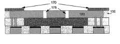
- the beam 160formed within dielectric layer 150 , is shown anchored at both ends. The center of the beam is designed to move vertically over cavity 120 (see FIG. 19A).
- the top surface 60 of the copper wiring 30 , 40 and 50is shown to be recessed to minimize stiction, preferably by way of a wet etch, although other means are suitable.
- the extent of the recessdepends upon the final structure desired.
- a wet etchconsisting of a dilute solution of acetic acid and hydrogen peroxide is generally used.
- the copperis preferably etched to a depth of about 800 Angstroms.
- FIG. 6shows a top-down view of the MEMS device illustrated in FIG. 5.
- Beam 160suspended over the cavity 120 , is shown having a plurality of holes 175 which will be described in more detail during the process description (FIGS. 9 - 19 ). These holes are useful to facilitate the removal of the sacrificial material when constructing the cavity 120 .
- FIG. 7shows a cross-section view of another type of MEMS device, wherein only one end of the switch is anchored.
- copper wiring 30 , 40 and 50are formed in dielectric layer 20
- vias 110are formed in dielectric layer 100 .
- Beam 160is unattached at one end, allowing it to freely move in a vertical motion over cavity 120 .
- FIG. 8is a corresponding top-down view of the MES device described in FIG. 7, again with moveable beam 160 being provided with holes 175 .
- FIG. 9there is shown the copper wiring 30 , 40 , and 50 formed in dielectric layer 20 , wherein the top surface of the wiring is substantially planar with respect to the top surface of dielectric layer 20 .
- the top surface 60 of the wiringis shown recessed with respect to the top layer of dielectric layer 20 .
- One method for recessing the metalis by way of a wet etch which is efficacious for that metal for the time required to achieve the desired depth.
- a solutionconsisting of water, acetic acid and hydrogen peroxide (3 liters, 15 ml and 9 ml, respectively) applied for 2.5 minutes achieves a depth of 600 to 800 Angstroms.
- barrier material 70is deposited to encapsulate the copper to protect it for the subsequent processing.
- the preferred embodimentincorporates a layer 100 Angstroms thick of Ta followed by 400 Angstroms of TaN.
- the barrier materialcan also be made of dielectric or of any number of other suitable metallic barriers.
- FIG. 12shows the result of removing the barrier 70 from the uppermost surface of dielectric 80 . This is best accomplished by a chemical-mechanical polish (CMP).
- CMPchemical-mechanical polish
- the barrier material 75is now left only in the recessed areas. Since the CMP process may erode some of the dielectric 20 , care must be taken to minimize erosion of the dielectric if one is to maintain a suitable gap 200 when the switch is closed.
- the depth from the upper dielectric 80 down to the barrier 75will be about 200 Angstroms. This can be customized in order to form the final gap for the capacitive switch.
- Another method of encapsulating the conductorsis to pattern the blanket barrier 70 with the same mask that defined the conductors, but with an opposite polarity photoresist, and etching the barrier layer from the uppermost surface.
- a metal contact switchone may encapsulate the lower electrode(s), especially 50 , to a level that is substantially planar with dielectric 20 or even slightly raised above that surface. In this configuration, when the switch is closed, a direct metal-to-metal contact is established between signal electrode 50 and beam 160 .
- the lower electrodescan be encapsulated with dielectric material, preferably, one having a high dielectric constant, in order to construct a metal-insulator-metal switch. This generates a capacitive switch similar to the preferred air gap switch without the advantages of the reduced contact area.
- dielectric layer 100is shown within which vias are fabricated using standard processing techniques.
- the thickness of dielectric layer 100depends on the required spacing between the lower electrodes and the upper beam to be formed later. In the preferred embodiment, dielectric 100 is about 1000 Angstroms thick.
- Vias 110are patterned, etched, filled and planarized according to standard damascene processing.
- FIG. 14shows the formation of cavity 120 etched in dielectric 100 .
- This cavityis fabricated using conventional photolithography and reactive-ion-etching (RIE). Care must be taken to ensure that the original structure of the lower electrodes 90 is preserved, i.e., ensuring that the relationship between the lower dielectric surface 80 and the recessed metal 75 is not altered. This relationship is not critical when constructing the metal-to-metal or metal-insulator- metal versions of the MEMS device.
- RIEreactive-ion-etching
- FIG. 15illustrates the structure after applying a sacrificial material 130 , such as SILK or DLC.
- SILKis a semiconductor dielectric manufactured by Dow Chemical Corp. This material includes various formulations of the product, known also under the name of Porous SiLK. It is a polymer resin comprised of gamma-butyrolactone, B-staged polymer and mesitylene.
- Another material which is preferentially usedis the aforementioned DLC, a diamond like carbon, which is an amorphous carbon containing a coating wherein a proportion of the carbon atoms is bonded in a similar manner to diamond and which resembles in many ways to diamond.
- Diamond-like carbonis produced when carbon is deposited under energetic bombardment. The instantaneous localized high temperature and pressure induce a proportion of the carbon atoms to bond as diamond. These conditions are obtained during plasma assisted chemical vapor deposition (PACVD).
- the depositionis done with carbon containing gas, such as acetylene, which is introduced to provide the energetic carbon ions.
- carbon containing gassuch as acetylene
- These materialscan be removed by way of oxygen plasma exposure if there is no oxidizable material that is exposed. If there is an oxidizable material that will be exposed during the removal of the organic material, then an H 2 /CO 2 /CO/N 2 type plasma removal is to be used. These gas mixtures will be recognizable to practitioners skilled in the art of reactive-ion-etch processes.
- the structureis finally planarized to an extent where it is substantially aligned with respect to the upper surface of dielectric 100 .
- the entire dielectric layer 100is formed of release material 100 A, such as SILK.
- release material 100 Asuch as SILK.
- the edges of the cavityare defined by the lateral removal of the release material.
- the materialis released by exposing it to an oxygen or hydrogen plasma which decomposes the material. Additional details may be found in the paper “Erosion of diamond films and graphite in oxygen plasma” by A. Joshi and R. Nimmagadda, published in the Journal of Materials Research., Vol. 6, No. 7, p. 1484, 1996, by the Materials Research Society.
- FIG. 17illustrates the formation of the level reserved for beam 160 .
- dielectric material 150is again deposited.
- the metal beam 160is preferably fabricated within dielectric 150 .
- the beammay be fixed at both ends, as shown in FIGS. 5 - 6 , or at one end as illustrated with reference to FIGS. 7 - 8 .
- the beammay be provided with holes 175 which are useful to subsequently facilitate the removal of the sacrificial material.
- the beammay also be encapsulated as described earlier with reference to FIGS. 11 - 12 , referenced by numeral 75 , in order to protect the copper.
- FIG. 18illustrates the photolithography and RIE steps to etch out the dielectric around and through the beam and over the cavity. This frees the moveable section of the beam 160 from the upper dielectric 150 and provides access to release material 130 .
- FIG. 19illustrates the structure after removal of the release material 130 . This is preferably done using an oxygen plasma to break down the organic materials that are present, allowing them to be evacuated. Following this step, encapsulation of the entire device may be performed using conventional methods or, alternatively, by pinching off the release holes in a dielectric covering, as will be described hereinafter with reference to FIGS. 22 - 25 .
- FIG. 19Adepicts the completed device in its closed state.
- Beam 160anchored at both ends, is shown with its center bent downwards.
- the drawingsare not to scale. Accordingly, in order to better visualize the final device and better understand its working, the true scale of the various parts of the device will be described.
- the cavity that defines the distance the beam is to movemay only be 200 to 1000 Angstroms for a moveable beam 10,000 Angstroms thick. Thus, the deformation of the beam is fairly minor.
- FIG. 20 through 23shows an alternate method to be inserted from FIG. 17 onward and which is useful to describe how to encapsulate the MEMS device.
- yet another dielectric layer 210is now added to form another cavity above the beam 220 (see FIG. 21).
- the dielectricis removed from the cavity area through and surrounding the beam.
- the etched areasare filled with more release material 230 as previously described, preferably, with SILK or DLC, and it is planarized.
- release material 230as previously described, preferably, with SILK or DLC, and it is planarized.
- the same sacrificial material that was placed belowis now used again, such that the release process removes all the layers of release material.
- FIG. 23illustrates the addition of yet another dielectric layer 240 within which vias 250 are patterned and etched. These vias provide access to the release material to be removed.
- FIG. 24shows the device with the release material removed through vias 250 , as described earlier.
- FIG. 25shows the final encapsulation step of depositing another dielectric 260 which pinches off the small vias 250 , thus sealing the structure.
- FIGS. 26 and 27illustrate an alternate method of making the cavitylvias dielectric layer entirely out of release material 100 A, as referenced in FIG. 16.
- FIG. 26shows the beam already formed and the upper cavity area 220 patterned and etched, as described earlier with reference to FIG. 21.
- the release process using the plasma processis shown in FIG. 27.
- the release processis isotropic and, thus, has a lateral removal rate.
- the lateral ratedepends on the release material used and the process by which it is removed.
- the release materialis removed directly below the open areas as well as at some lateral distance 250 from each boundary.
Landscapes
- Engineering & Computer Science (AREA)
- Manufacturing & Machinery (AREA)
- Microelectronics & Electronic Packaging (AREA)
- Power Engineering (AREA)
- Physics & Mathematics (AREA)
- Geometry (AREA)
- Micromachines (AREA)
- Surface Acoustic Wave Elements And Circuit Networks Thereof (AREA)
- Manufacture Of Macromolecular Shaped Articles (AREA)
- Manufacture Of Switches (AREA)
Abstract
Description
- This invention generally relates to the fabrication of micro-electromechanical switches (MEMS), and more particularly, to the manufacture of MEMS which can be integrated into current state of the art semiconductor fabrication processes.[0001]
- Switching operations are a fundamental part of many electrical, mechanical and electromechanical applications. MEM switches have drawn considerable interest over the last few years. Products using MEMS technology are widespread in biomedical, aerospace, and communications systems.[0002]
- Conventional MEMS typically utilize cantilever switches, membrane switches, and tunable capacitor structures as described, e.g., in U.S. Pat. No. 6,160,230 to McMillan et al., U.S. Pat. No. 6,143,997 to Feng et al., U.S. Pat. No. 5,970,315 to Carley et al., and U.S. Pat. No. 5,880,921 to Tham et al. MEMS devices are manufactured using micro-electromechanical techniques and are used to control electrical, mechanical or optical signal flows. Such devices, however, present many problems because their structure and innate material properties require them to be manufactured in lines that are separate from conventional semiconductor processing. This is usually due to the different materials and processes which are not compatible and, therefore, which cannot be integrated in standard semiconductor fabrication processes.[0003]
- The use of materials typically used in the manufacture of MEMS, such as gold, pose obvious integration problems for integrating devices directly to on-chip applications. Even the use of polysilicon, which is widely found in the literature, poses problems due to the temperature cycles and the usual segregation of front-end of the line (FEOL) tools where the actual semiconductor devices are fabricated and the back-end of the line (BEOL) where interconnect metals are processed. Typically, the two sets are not allowed to have process crossovers from one to the other in order to prevent metallic contamination of the active devices. It is therefore unlikely to see polysilicon deposition in the back-end of the line.[0004]
- Most existing processes suffer from a serious drawback in that by using standard metalization, no encapsulation is provided to protect the metal. Moreover, more than one substrate is used, oftentimes bonded together, with corresponding inherent disadvantages.[0005]
- Other existing techniques only provide switching capabilities at the top of the structure, making it unlikely that integration can be achieved at all levels, as will be described hereinafter in the present invention.[0006]
- Accordingly, there is a need for a process that is capable of providing MEMS devices using established BEOL materials coupled to processing that can be fully integrated so that these devices can be manufactured either in conjunction with or as an add-on module to the conventional BEOL or interconnect levels.[0007]
- In order to gain a better understanding of the present invention, a conventional MEM switch will now be described with reference to FIG. 1, which shows a cross-section view of a MEM switch having both ends of a deformable beam[0008]1 anchored in dielectric4. The lowest level consists of a
dielectric material 5 containing conductive elements2,2a, and3 which will be used subsequently to connect or form the various electrical portions of the device. The conductors referenced by numerals2 and2aare used to provide an operating potential that causes the beam to deform. Conductor3, which conducts a signal, is in turn connected to the beam when it is in operation. - FIG. 2 shows a planar view of the same prior art MEM device of FIG. 1. In a typical implementation, deformable beam[0009]1 is formed by polysilicon over dielectric4, e.g., SiO2, and the surrounding material is etched away leaving a raised structure, i.e., the beam suspended above the conductors that were previously formed or which, themselves, are made of polysilicon. Then the device is subjected to electroless plating, usually of gold, that adheres to the polysilicon forming the conductive elements1,2,2aand3. The switch is operated by providing a potential difference between the beam and electrodes2 and2a. This voltage generates an electrostatic attraction which pulls beam1 in contact with electrode3, thus closing the switch.
- One should note that these are all typically raised structures having a large topography when compared to conventional semiconductor devices. This in itself makes them virtually impossible to integrate into the semiconductor chip fabrication process. These devices are typically made using surface micro-machining techniques which include building on photoresist or building on a substrate, such as silicon, and then removing a portion of the substrate under the device from the backside of the substrate, again precluding integration with standard semiconductor processing.[0010]
- FIG. 3 illustrates a cross-section view of another version of a conventional MEM switch, wherein only one end of the beam[0011]1 is anchored within the dielectric4. All the other parts perform as described in FIG. 1. The same applies with regard to FIG. 4, illustrating a top-down view of the corresponding device illustrated in FIG. 3. In the latter case, the switch is operated by applying a voltage between beam1 and control electrode2. This causes the beam to be pulled down into contact with the signal electrode3. When the voltage is dropped, beam1 returns to its original position.
- Typically, the gap between the beam and the control electrode substantially determines the voltage required to pull down the beam. Most literature describes devices having gaps ranging from 1 to several micrometers. These gaps are large and the voltage required is therefore higher than would be desired for most consumer applications. Reported activation voltages range from around 30 to 75 volts. This is far too high for applications like cell phones which typically operate between 3 to 5 volts. The structure of the present invention operates with gaps ranging from 200 angstroms to several thousand angstroms, producing switches having an activation voltage below 5 volts.[0012]
- The aforementioned illustrative switch configurations are only some of many possible structures which are known in the art. It is worth noting that MEM switches may also be configured in an arrangement of multiple beams wired in a variety of combinations.[0013]
- Stiction is of primary concern in MEMS devices. Stiction is defined as two or more surface making contact that will not release without causing some damage to the device. Impingement is a major cause of this phenomena. The present invention addresses this problem in at least one embodiment by providing an[0014]
air gap 200 when the switch is closed, as will be shown in detail with reference to FIG. 19A. Surface tension is also believed to be another major cause of stiction. That explains why the present invention utilizes dry etches and processes for the release of the moving parts and subsequent processing. - Accordingly, it is an object of the invention to build MEM switches and other similar structures which are fully integrated within CMOS, bipolar or BiCMOS wafers.[0015]
- It is another object to manufacture MEM switches and other similar structures with a modified damascene process.[0016]
- It is a further object to build MEM switches and other similar structures utilizing copper encapsulated in a barrier material to protect the metal.[0017]
- It is yet another object to ensure that the encapsulation can be integrated into BEOL copper at a temperature compatible with such a process.[0018]
- These and other objects are addressed by the present invention by providing a method of fabricating MEMS switches integrated with conventional semiconductor interconnect levels, using compatible processes and materials.[0019]
- The invention described herein provides a method of fabricating a capacitive switch adaptable to produce various configurations used for contact switching and/or metal-dielectric- metal switches.[0020]
- In a preferred embodiment, the process starts with a copper damascene interconnect layer made of metal conductors inlaid within a dielectric. All or portions of the copper interconnects are recessed to a degree sufficient to provide a capacitive air gap when the switch is closed and, additionally, to provide a space for a protective layer of Ta/TaN, if so desired. The metal structures that are defined within the area specified by the switch act as actuator electrodes to pull down a moveable conductive beam providing one or more paths for the switching signals to traverse. The advantage of such air gap is that the dielectric (air) is not subject to charge storage or trapping that causes reliability and voltage drift problems.[0021]
- The present invention can be embodied using any number of dielectric materials, such as silicon dioxide or silicon nitride, all of which may advantageously be placed between the lower electrodes and the deformable beam of the capacitive switch.[0022]
- It is worth noting that instead of recessing the electrodes to provide a gap, one may just add dielectric around and/or on the electrode. A second dielectric layer is then deposited to the desired thickness of the gap formed between the lower electrodes and the moveable beam. Vias are the formed through the second dielectric layer to provide connections between the aforementioned metal interconnect layer and the next metal layer which includes the movable beam. The layer containing the vias is then patterned and etched to provide a cavity area which contains the lower activation electrodes as well as the signal paths. The cavity is then back-filled with sacrificial release material, preferably SiLK, which is a semiconductor dielectric in the form of a polymer resin consisting of gamma-butyrolactone, B-staged polymer and mesitylene. This release material is then made substantially planar, preferably, by way of chemical-mechanical polish (CMP) to align it with the top of the dielectric. It is also possible to planarize the release material by re-imaging the same mask that was used to define the cavity area using the opposite polarity photoresist and then etching the release material from the upper surface to make it substantially co-planar with the dielectric in which the cavity was formed. This provides a planar surface upon which the beam layer can be constructed.[0023]
- The layer containing the movable beam is similar to other interconnect layers typically used for the fabrication of standard CMOS devices. The beam structure preferably extends, partially or completely, across the cavity area previously defined, such that when the switch is in operation, it provides the desired electrical connections. It should also be noted that holes may be incorporated into the moveable beam. These holes are initially filled with the same dielectric that forms the layer containing the beam. These areas of dielectric within the beam are then etched out to provide greater access to the sacrificial material under the beam and, thus, aiding the release process. Next, the pattern of the cavity area or some subset of the pattern is defined and the dielectric material surrounding the beam is removed, including areas through the holes in the beam, providing access to the underlying release material. At this point the released material can be removed. The switch, suspended over the cavity area is now fully functional.[0024]
- The foregoing and other objects, aspects and advantages of the invention will be better understood from the following detailed description of a preferred embodiment of the invention with reference to the accompanying drawings, in which:[0025]
- FIGS. 1 and 2 respectively show a cross-sectional view and a top-down view seen along the length of the beam of a prior art MEM switch, wherein both ends of the beam are anchored;[0026]
- FIGS. 3 and 4 respectively show a cross-sectional and a top-down view of another type of a prior art MEM switch wherein only one end of the beam is anchored;[0027]
- FIGS. 5 and 6 are, respectively, a cross-sectional view and top-down view of a MEM switch fabricated in accordance with the present invention, with both ends of the beam anchored;[0028]
- FIGS. 7 and 8 show respectively cross-sectional and top-down views of a MEM switch fabricated in accordance with the present invention, wherein only one end of the beam is anchored;[0029]
- FIGS.[0030]9-19 illustrate the series of steps required to fabricate the MEMS device, in accordance to a preferred embodiment of the invention;
- FIG. 19A shows the completed MEM switch, according to the invention, in its closed position.[0031]
- FIGS.[0032]20-25 show an alternate process flow providing a fully encapsulated version of the MEM switch of the preferred embodiment.
- FIGS. 26 and 27 illustrate an alternative process of making the cavity and vias dielectric layer entirely out of the release material.[0033]
- The primary embodiment teaches building a MEMS device in a way that may be fully integrated into a standard CMOS, bipolar, BiCMOS or other common semiconductor chip process.[0034]
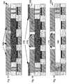
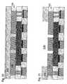
- FIG. 5 illustrates the initial structure, i.e., a copper damascene interconnect layer. Underlying this, may be placed devices such as FETs, NPN transistors or HBTs (Hetero-junction Bipolar Transistors), resistors, etc., on a silicon substrate or, alternatively, on a low-loss substrate, preferably made of SiO[0035]2. It consists of
copper wiring dielectric layer 20, preferably made of SiO2. The area referenced bynumeral 30 represents the landing metal forvias 110 embedded indielectric layer 100. The metal referenced by numeral40 forms the actuator or control electrodes, andmetal 50 represents the signal electrode. The thickness of the metal is typically on the order of 3000 to 5000 Angstroms, but it is not limited to this range. Thebeam 160, formed withindielectric layer 150, is shown anchored at both ends. The center of the beam is designed to move vertically over cavity120 (see FIG. 19A). - Still referring to FIG. 5, the[0036]
top surface 60 of thecopper wiring - FIG. 6 shows a top-down view of the MEMS device illustrated in FIG. 5.[0037]
Beam 160, suspended over thecavity 120, is shown having a plurality ofholes 175 which will be described in more detail during the process description (FIGS.9-19). These holes are useful to facilitate the removal of the sacrificial material when constructing thecavity 120. - FIG. 7 shows a cross-section view of another type of MEMS device, wherein only one end of the switch is anchored. As in FIG. 5,[0038]
copper wiring dielectric layer 20, whereasvias 110 are formed indielectric layer 100.Beam 160 is unattached at one end, allowing it to freely move in a vertical motion overcavity 120. - FIG. 8 is a corresponding top-down view of the MES device described in FIG. 7, again with[0039]
moveable beam 160 being provided withholes 175. - The process used to construct the MEM switches illustrated in FIGS.[0040]5-6 and7-8 will now be described in detail.
- Referring to FIG. 9, there is shown the[0041]
copper wiring dielectric layer 20, wherein the top surface of the wiring is substantially planar with respect to the top surface ofdielectric layer 20. - Next, and with reference to FIG. 10, the[0042]
top surface 60 of the wiring is shown recessed with respect to the top layer ofdielectric layer 20. One method for recessing the metal is by way of a wet etch which is efficacious for that metal for the time required to achieve the desired depth. For instance, in the preferred embodiment, a solution consisting of water, acetic acid and hydrogen peroxide (3 liters, 15 ml and 9 ml, respectively) applied for 2.5 minutes achieves a depth of 600 to 800 Angstroms. - Referring now to FIG. 11, a layer of[0043]
barrier material 70 is deposited to encapsulate the copper to protect it for the subsequent processing. The preferred embodiment incorporates alayer 100 Angstroms thick of Ta followed by 400 Angstroms of TaN. Alternatively, the barrier material can also be made of dielectric or of any number of other suitable metallic barriers. - FIG. 12 shows the result of removing the[0044]
barrier 70 from the uppermost surface ofdielectric 80. This is best accomplished by a chemical-mechanical polish (CMP). Thebarrier material 75 is now left only in the recessed areas. Since the CMP process may erode some of the dielectric20, care must be taken to minimize erosion of the dielectric if one is to maintain asuitable gap 200 when the switch is closed. When the CMP process is completed, the depth from theupper dielectric 80 down to thebarrier 75 will be about 200 Angstroms. This can be customized in order to form the final gap for the capacitive switch. - Another method of encapsulating the conductors is to pattern the[0045]
blanket barrier 70 with the same mask that defined the conductors, but with an opposite polarity photoresist, and etching the barrier layer from the uppermost surface. - In a variation to the preferred embodiment, and referring to any of FIGS. 5 through 8, one may modify the recess and/or the depositions to achieve a planar or even a raised metal contact to fabricate a metal-to-metal contact switch or a metal-insulator-metal switch. In the case of a metal contact switch, one may encapsulate the lower electrode(s), especially[0046]50, to a level that is substantially planar with dielectric20 or even slightly raised above that surface. In this configuration, when the switch is closed, a direct metal-to-metal contact is established between
signal electrode 50 andbeam 160. Similarly, the lower electrodes can be encapsulated with dielectric material, preferably, one having a high dielectric constant, in order to construct a metal-insulator-metal switch. This generates a capacitive switch similar to the preferred air gap switch without the advantages of the reduced contact area. - Referring now to FIG. 13, the addition of another[0047]
dielectric layer 100 is shown within which vias are fabricated using standard processing techniques. The thickness ofdielectric layer 100 depends on the required spacing between the lower electrodes and the upper beam to be formed later. In the preferred embodiment, dielectric100 is about 1000 Angstroms thick.Vias 110 are patterned, etched, filled and planarized according to standard damascene processing. - FIG. 14 shows the formation of[0048]
cavity 120 etched indielectric 100. This cavity is fabricated using conventional photolithography and reactive-ion-etching (RIE). Care must be taken to ensure that the original structure of thelower electrodes 90 is preserved, i.e., ensuring that the relationship between thelower dielectric surface 80 and the recessedmetal 75 is not altered. This relationship is not critical when constructing the metal-to-metal or metal-insulator- metal versions of the MEMS device. - FIG. 15 illustrates the structure after applying a sacrificial material[0049]130, such as SILK or DLC. [Note: SILK is a semiconductor dielectric manufactured by Dow Chemical Corp. This material includes various formulations of the product, known also under the name of Porous SiLK. It is a polymer resin comprised of gamma-butyrolactone, B-staged polymer and mesitylene. Another material which is preferentially used is the aforementioned DLC, a diamond like carbon, which is an amorphous carbon containing a coating wherein a proportion of the carbon atoms is bonded in a similar manner to diamond and which resembles in many ways to diamond. Other organic materials that are capable of being volatized in a similar manner will be described. Diamond-like carbon is produced when carbon is deposited under energetic bombardment. The instantaneous localized high temperature and pressure induce a proportion of the carbon atoms to bond as diamond. These conditions are obtained during plasma assisted chemical vapor deposition (PACVD). The deposition is done with carbon containing gas, such as acetylene, which is introduced to provide the energetic carbon ions. These materials can be removed by way of oxygen plasma exposure if there is no oxidizable material that is exposed. If there is an oxidizable material that will be exposed during the removal of the organic material, then an H2/CO2/CO/N2type plasma removal is to be used. These gas mixtures will be recognizable to practitioners skilled in the art of reactive-ion-etch processes. The structure is finally planarized to an extent where it is substantially aligned with respect to the upper surface of
dielectric 100. - In another embodiment of the invention, shown in FIG. 16, the entire[0050]
dielectric layer 100 is formed of release material100A, such as SILK. This allows eliminating the steps of forming the bottom cavity120 (see FIG. 14) since the area evacuated can be defined later, as will be shown in FIGS. 26 and 27. The edges of the cavity are defined by the lateral removal of the release material. The material is released by exposing it to an oxygen or hydrogen plasma which decomposes the material. Additional details may be found in the paper “Erosion of diamond films and graphite in oxygen plasma” by A. Joshi and R. Nimmagadda, published in the Journal of Materials Research., Vol. 6, No. 7, p. 1484, 1996, by the Materials Research Society. - FIG. 17 illustrates the formation of the level reserved for[0051]
beam 160. To this end, it may be useful to refer back to FIGS.5-8 for better understanding the structure. At the beam level,dielectric material 150 is again deposited. Themetal beam 160 is preferably fabricated withindielectric 150. The beam may be fixed at both ends, as shown in FIGS.5-6, or at one end as illustrated with reference to FIGS.7-8. As previously mentioned, the beam may be provided withholes 175 which are useful to subsequently facilitate the removal of the sacrificial material. The beam may also be encapsulated as described earlier with reference to FIGS.11-12, referenced bynumeral 75, in order to protect the copper. - FIG. 18 illustrates the photolithography and RIE steps to etch out the dielectric around and through the beam and over the cavity. This frees the moveable section of the[0052]
beam 160 from theupper dielectric 150 and provides access to release material130. - FIG. 19 illustrates the structure after removal of the release material[0053]130. This is preferably done using an oxygen plasma to break down the organic materials that are present, allowing them to be evacuated. Following this step, encapsulation of the entire device may be performed using conventional methods or, alternatively, by pinching off the release holes in a dielectric covering, as will be described hereinafter with reference to FIGS.22-25.
- FIG. 19A depicts the completed device in its closed state.[0054]
Beam 160, anchored at both ends, is shown with its center bent downwards. The drawings are not to scale. Accordingly, in order to better visualize the final device and better understand its working, the true scale of the various parts of the device will be described. For example, the cavity that defines the distance the beam is to move, may only be 200 to 1000 Angstroms for a moveable beam 10,000 Angstroms thick. Thus, the deformation of the beam is fairly minor. - FIGS. 20 through 23 shows an alternate method to be inserted from FIG. 17 onward and which is useful to describe how to encapsulate the MEMS device. Referring to FIG. 20, yet another[0055]
dielectric layer 210 is now added to form another cavity above the beam220 (see FIG. 21). When etching theupper cavity 220, the dielectric is removed from the cavity area through and surrounding the beam. - Next, in FIG. 22 the etched areas are filled with more release material[0056]230 as previously described, preferably, with SILK or DLC, and it is planarized. The same sacrificial material that was placed below is now used again, such that the release process removes all the layers of release material.
- FIG. 23 illustrates the addition of yet another[0057]
dielectric layer 240 within which vias250 are patterned and etched. These vias provide access to the release material to be removed. - FIG. 24 shows the device with the release material removed through[0058]
vias 250, as described earlier. - FIG. 25 shows the final encapsulation step of depositing another dielectric[0059]260 which pinches off the
small vias 250, thus sealing the structure. - FIGS. 26 and 27 illustrate an alternate method of making the cavitylvias dielectric layer entirely out of release material[0060]100A, as referenced in FIG. 16. FIG. 26 shows the beam already formed and the
upper cavity area 220 patterned and etched, as described earlier with reference to FIG. 21. - Next, the release process using the plasma process is shown in FIG. 27. The release process is isotropic and, thus, has a lateral removal rate. The lateral rate depends on the release material used and the process by which it is removed. The release material is removed directly below the open areas as well as at some[0061]
lateral distance 250 from each boundary. While the invention has been described in conjunction with a preferred embodiment, it is to be understood that many alternatives, modifications and variations will be apparent to those skilled in the art in light of the aforementioned description. Accordingly, it is intended to embrace all such alternatives, modifications and variations which fall within the spirit and scope of the appended claims. All matters set forth herein or shown in the accompanying drawings are to be interpreted in an illustrative and non-limiting sense.
Claims (17)
Priority Applications (12)
| Application Number | Priority Date | Filing Date | Title |
|---|---|---|---|
| US10/014,660US6635506B2 (en) | 2001-11-07 | 2001-11-07 | Method of fabricating micro-electromechanical switches on CMOS compatible substrates |
| TW091125027ATW590983B (en) | 2001-11-07 | 2002-10-25 | Method of fabricating micro-electromechanical switches on CMOS compatible substrates |
| PCT/US2002/036088WO2003054938A1 (en) | 2001-11-07 | 2002-11-07 | Method of fabricating micro-electromechanical switches on cmos compatible substrates |
| KR1020047001481AKR100586771B1 (en) | 2001-11-07 | 2002-11-07 | How to fabricate a microelectromechanical switch on a CMOS compatible substrate |
| AU2002365158AAU2002365158A1 (en) | 2001-11-07 | 2002-11-07 | Method of fabricating micro-electromechanical switches on cmos compatible substrates |
| CNB028211618ACN1309019C (en) | 2001-11-07 | 2002-11-07 | Method of fabricating micro-electromechanical switches on CMOS compatible substrates |
| JP2003555566AJP4081012B2 (en) | 2001-11-07 | 2002-11-07 | Method for fabricating a microelectromechanical switch on a CMOS compatible substrate |
| EP02803310AEP1461828B1 (en) | 2001-11-07 | 2002-11-07 | Method of fabricating micro-electromechanical switches on cmos compatible substrates |
| IL16165402AIL161654A0 (en) | 2001-11-07 | 2002-11-07 | Method of fabricating micro-electromechanical switches on cmos compatible substrates |
| DE60224836TDE60224836T2 (en) | 2001-11-07 | 2002-11-07 | METHOD FOR PRODUCING ELECTROMECHANIC MICROSWITCHES ON CMOS COMPATIBLE SUBSTRATES |
| AT02803310TATE384685T1 (en) | 2001-11-07 | 2002-11-07 | METHOD FOR PRODUCING ELECTROMECHANICAL MICROSWITCHES ON CMOS COMPATIBLE SUBSTRATES |
| IL161654AIL161654A (en) | 2001-11-07 | 2004-04-29 | Method of fabricating micro-electromechanical switches on cmos compatible substrates |
Applications Claiming Priority (1)
| Application Number | Priority Date | Filing Date | Title |
|---|---|---|---|
| US10/014,660US6635506B2 (en) | 2001-11-07 | 2001-11-07 | Method of fabricating micro-electromechanical switches on CMOS compatible substrates |
Related Child Applications (1)
| Application Number | Title | Priority Date | Filing Date |
|---|---|---|---|
| US10/434,999DivisionUS6798029B2 (en) | 2003-05-09 | 2003-05-09 | Method of fabricating micro-electromechanical switches on CMOS compatible substrates |
Publications (2)
| Publication Number | Publication Date |
|---|---|
| US20030148550A1true US20030148550A1 (en) | 2003-08-07 |
| US6635506B2 US6635506B2 (en) | 2003-10-21 |
Family
ID=21766896
Family Applications (1)
| Application Number | Title | Priority Date | Filing Date |
|---|---|---|---|
| US10/014,660Expired - LifetimeUS6635506B2 (en) | 2001-11-07 | 2001-11-07 | Method of fabricating micro-electromechanical switches on CMOS compatible substrates |
Country Status (11)
| Country | Link |
|---|---|
| US (1) | US6635506B2 (en) |
| EP (1) | EP1461828B1 (en) |
| JP (1) | JP4081012B2 (en) |
| KR (1) | KR100586771B1 (en) |
| CN (1) | CN1309019C (en) |
| AT (1) | ATE384685T1 (en) |
| AU (1) | AU2002365158A1 (en) |
| DE (1) | DE60224836T2 (en) |
| IL (2) | IL161654A0 (en) |
| TW (1) | TW590983B (en) |
| WO (1) | WO2003054938A1 (en) |
Cited By (25)
| Publication number | Priority date | Publication date | Assignee | Title |
|---|---|---|---|---|
| US20040097003A1 (en)* | 2002-11-20 | 2004-05-20 | International Business Machines Corporation | MEMS encapsulated structure and method of making same |
| US20040145874A1 (en)* | 2003-01-23 | 2004-07-29 | Stephane Pinel | Method, system, and apparatus for embedding circuits |
| WO2006046194A1 (en) | 2004-10-27 | 2006-05-04 | Koninklijke Philips Electronics N. V. | Reduction of air damping in mems device |
| US20060214246A1 (en)* | 2005-03-24 | 2006-09-28 | Garcia Jason A | Methods and apparatuses for microelectronic assembly having a material with a variable viscosity around a MEMS device |
| US20070004096A1 (en)* | 2003-12-24 | 2007-01-04 | Heuvelman Willem M | Method for containing a device and a corresponding device |
| CN100412607C (en)* | 2003-09-29 | 2008-08-20 | 松下电器产业株式会社 | Micro electromechanical system and manufacturing method thereof |
| US20090215214A1 (en)* | 2008-02-22 | 2009-08-27 | Mickael Renault | Method of Sealing a Cavity |
| US7595209B1 (en)* | 2007-03-09 | 2009-09-29 | Silicon Clocks, Inc. | Low stress thin film microshells |
| US20090275163A1 (en)* | 2008-04-30 | 2009-11-05 | Joseph Damian Gordon Lacey | System and Method of Encapsulation |
| US7659150B1 (en) | 2007-03-09 | 2010-02-09 | Silicon Clocks, Inc. | Microshells for multi-level vacuum cavities |
| US7736929B1 (en) | 2007-03-09 | 2010-06-15 | Silicon Clocks, Inc. | Thin film microshells incorporating a getter layer |
| US20100248484A1 (en)* | 2009-03-26 | 2010-09-30 | Christopher Bower | Methods of Forming Printable Integrated Circuit Devices and Devices Formed Thereby |
| US20110079495A1 (en)* | 2009-10-01 | 2011-04-07 | Knipe Richard L | Micromechanical digital capacitor with improved rf hot switching performance and reliability |
| US7923790B1 (en) | 2007-03-09 | 2011-04-12 | Silicon Laboratories Inc. | Planar microshells for vacuum encapsulated devices and damascene method of manufacture |
| US20120055768A1 (en)* | 2009-03-11 | 2012-03-08 | Nxp B.V. | Mems electrostatic actuator |
| WO2011162953A3 (en)* | 2010-06-25 | 2012-04-19 | International Business Machines Corporation | Planar cavity mems and related structures, methods of manufacture and design structures |
| US20120112294A1 (en)* | 2010-11-05 | 2012-05-10 | Nxp B.V. | Ic manufacturing method, ic and apparatus |
| US8508003B2 (en) | 2009-04-24 | 2013-08-13 | Murata Manufacturing Co., Ltd. | MEMS element and method for manufacturing same |
| US20130335878A1 (en)* | 2012-06-14 | 2013-12-19 | Cavendish Kinetics Inc. | Mems lifetime enhancement |
| US8643140B2 (en)* | 2011-07-11 | 2014-02-04 | United Microelectronics Corp. | Suspended beam for use in MEMS device |
| EP2365521A3 (en)* | 2010-01-22 | 2014-06-04 | Imec | Thin film wafer level package |
| US20150217995A1 (en)* | 2013-09-27 | 2015-08-06 | Weng Hong Teh | Arrangement of through-hole structures of a semiconductor package |
| US9422149B2 (en) | 2014-07-25 | 2016-08-23 | Semiconductor Manufacturing International (Shanghai) Corporation | Trapped sacrificial structures and methods of manufacturing same using thin-film encapsulation |
| US10319680B1 (en) | 2018-03-01 | 2019-06-11 | Sandisk Technologies Llc | Metal contact via structure surrounded by an air gap and method of making thereof |
| US10508961B2 (en) | 2012-06-28 | 2019-12-17 | Intel Corporation | Semiconductor package with air pressure sensor |
Families Citing this family (90)
| Publication number | Priority date | Publication date | Assignee | Title |
|---|---|---|---|---|
| US7550794B2 (en) | 2002-09-20 | 2009-06-23 | Idc, Llc | Micromechanical systems device comprising a displaceable electrode and a charge-trapping layer |
| US6291425B1 (en)* | 1999-09-01 | 2001-09-18 | Guilford Pharmaceuticals Inc. | Compounds, methods and pharmaceutical compositions for treating cellular damage, such as neural or cardiovascular tissue damage |
| US6643165B2 (en)* | 2001-07-25 | 2003-11-04 | Nantero, Inc. | Electromechanical memory having cell selection circuitry constructed with nanotube technology |
| US6876046B2 (en)* | 2002-02-07 | 2005-04-05 | Superconductor Technologies, Inc. | Stiction alleviation using passivation layer patterning |
| US6770569B2 (en)* | 2002-08-01 | 2004-08-03 | Freescale Semiconductor, Inc. | Low temperature plasma Si or SiGe for MEMS applications |
| JP4007115B2 (en)* | 2002-08-09 | 2007-11-14 | ソニー株式会社 | Micromachine and manufacturing method thereof |
| US7388259B2 (en)* | 2002-11-25 | 2008-06-17 | International Business Machines Corporation | Strained finFET CMOS device structures |
| JP4007172B2 (en) | 2002-12-03 | 2007-11-14 | ソニー株式会社 | Micromachine and manufacturing method thereof |
| US7202764B2 (en)* | 2003-07-08 | 2007-04-10 | International Business Machines Corporation | Noble metal contacts for micro-electromechanical switches |
| US7410846B2 (en)* | 2003-09-09 | 2008-08-12 | International Business Machines Corporation | Method for reduced N+ diffusion in strained Si on SiGe substrate |
| US6890808B2 (en)* | 2003-09-10 | 2005-05-10 | International Business Machines Corporation | Method and structure for improved MOSFETs using poly/silicide gate height control |
| US6887751B2 (en)* | 2003-09-12 | 2005-05-03 | International Business Machines Corporation | MOSFET performance improvement using deformation in SOI structure |
| US7170126B2 (en)* | 2003-09-16 | 2007-01-30 | International Business Machines Corporation | Structure of vertical strained silicon devices |
| DE10347215A1 (en) | 2003-10-10 | 2005-05-12 | Bosch Gmbh Robert | Micromechanical sensor |
| US7119403B2 (en) | 2003-10-16 | 2006-10-10 | International Business Machines Corporation | High performance strained CMOS devices |
| US7122849B2 (en)* | 2003-11-14 | 2006-10-17 | International Business Machines Corporation | Stressed semiconductor device structures having granular semiconductor material |
| JP2005197415A (en)* | 2004-01-06 | 2005-07-21 | Sony Corp | Semiconductor device and leak control circuit |
| US7202132B2 (en) | 2004-01-16 | 2007-04-10 | International Business Machines Corporation | Protecting silicon germanium sidewall with silicon for strained silicon/silicon germanium MOSFETs |
| JP4447940B2 (en)* | 2004-02-27 | 2010-04-07 | 富士通株式会社 | Microswitching device manufacturing method and microswitching device |
| US7923782B2 (en)* | 2004-02-27 | 2011-04-12 | International Business Machines Corporation | Hybrid SOI/bulk semiconductor transistors |
| US7205206B2 (en)* | 2004-03-03 | 2007-04-17 | International Business Machines Corporation | Method of fabricating mobility enhanced CMOS devices |
| US7504693B2 (en) | 2004-04-23 | 2009-03-17 | International Business Machines Corporation | Dislocation free stressed channels in bulk silicon and SOI CMOS devices by gate stress engineering |
| US7005371B2 (en)* | 2004-04-29 | 2006-02-28 | International Business Machines Corporation | Method of forming suspended transmission line structures in back end of line processing |
| US7223994B2 (en) | 2004-06-03 | 2007-05-29 | International Business Machines Corporation | Strained Si on multiple materials for bulk or SOI substrates |
| TWI463526B (en)* | 2004-06-24 | 2014-12-01 | Ibm | Method for improving stress-induced CMOS components and components prepared by the method |
| CN1309040C (en)* | 2004-06-29 | 2007-04-04 | 北京大学 | A method for integrating CMOS circuit and bulk silicon MEMS uniwafer |
| US7288443B2 (en)* | 2004-06-29 | 2007-10-30 | International Business Machines Corporation | Structures and methods for manufacturing p-type MOSFET with graded embedded silicon-germanium source-drain and/or extension |
| US7384829B2 (en) | 2004-07-23 | 2008-06-10 | International Business Machines Corporation | Patterned strained semiconductor substrate and device |
| US7088153B2 (en)* | 2004-08-05 | 2006-08-08 | International Business Machines Corporation | Data storage latch structure with micro-electromechanical switch |
| US7091765B2 (en)* | 2004-09-30 | 2006-08-15 | International Business Machines Corporation | Circuit power reduction using micro-electromechanical switches |
| US7173312B2 (en)* | 2004-12-15 | 2007-02-06 | International Business Machines Corporation | Structure and method to generate local mechanical gate stress for MOSFET channel mobility modification |
| US7274084B2 (en)* | 2005-01-12 | 2007-09-25 | International Business Machines Corporation | Enhanced PFET using shear stress |
| US20060160317A1 (en)* | 2005-01-18 | 2006-07-20 | International Business Machines Corporation | Structure and method to enhance stress in a channel of cmos devices using a thin gate |
| US7224033B2 (en) | 2005-02-15 | 2007-05-29 | International Business Machines Corporation | Structure and method for manufacturing strained FINFET |
| JP4724488B2 (en) | 2005-02-25 | 2011-07-13 | 日立オートモティブシステムズ株式会社 | Integrated microelectromechanical system |
| DE102005016243B3 (en)* | 2005-04-08 | 2006-09-28 | Austriamicrosystems Ag | Micromechanical component e.g. micro electro mechanical system structure, for use as e.g. micro sensor, has one metal layer of multi-layer structure extending at side over pile and electrically conductive membrane integrated in structure |
| US7288464B2 (en)* | 2005-04-11 | 2007-10-30 | Hewlett-Packard Development Company, L.P. | MEMS packaging structure and methods |
| US7545004B2 (en)* | 2005-04-12 | 2009-06-09 | International Business Machines Corporation | Method and structure for forming strained devices |
| US20060234412A1 (en)* | 2005-04-19 | 2006-10-19 | Hewlett-Packard Development Company, L.P. Intellectual Property Administration | MEMS release methods |
| US7544577B2 (en)* | 2005-08-26 | 2009-06-09 | International Business Machines Corporation | Mobility enhancement in SiGe heterojunction bipolar transistors |
| JP4713990B2 (en)* | 2005-09-13 | 2011-06-29 | 株式会社東芝 | Semiconductor device and manufacturing method thereof |
| US7300813B2 (en) | 2005-09-20 | 2007-11-27 | Dongguk University Indusrty-Academic Cooperation Foundation | Method for manufacturing micro-machined switch using pull-up type contact pad |
| US7202513B1 (en)* | 2005-09-29 | 2007-04-10 | International Business Machines Corporation | Stress engineering using dual pad nitride with selective SOI device architecture |
| US7655511B2 (en) | 2005-11-03 | 2010-02-02 | International Business Machines Corporation | Gate electrode stress control for finFET performance enhancement |
| US20070099360A1 (en)* | 2005-11-03 | 2007-05-03 | International Business Machines Corporation | Integrated circuits having strained channel field effect transistors and methods of making |
| US7785950B2 (en)* | 2005-11-10 | 2010-08-31 | International Business Machines Corporation | Dual stress memory technique method and related structure |
| US7709317B2 (en)* | 2005-11-14 | 2010-05-04 | International Business Machines Corporation | Method to increase strain enhancement with spacerless FET and dual liner process |
| US7348638B2 (en)* | 2005-11-14 | 2008-03-25 | International Business Machines Corporation | Rotational shear stress for charge carrier mobility modification |
| US7564081B2 (en) | 2005-11-30 | 2009-07-21 | International Business Machines Corporation | finFET structure with multiply stressed gate electrode |
| JP2007157511A (en)* | 2005-12-06 | 2007-06-21 | Hitachi Ltd | Switch using microelectromechanical system |
| US7776695B2 (en)* | 2006-01-09 | 2010-08-17 | International Business Machines Corporation | Semiconductor device structure having low and high performance devices of same conductive type on same substrate |
| US7635620B2 (en) | 2006-01-10 | 2009-12-22 | International Business Machines Corporation | Semiconductor device structure having enhanced performance FET device |
| US20070158743A1 (en)* | 2006-01-11 | 2007-07-12 | International Business Machines Corporation | Thin silicon single diffusion field effect transistor for enhanced drive performance with stress film liners |
| JP2007210083A (en)* | 2006-02-13 | 2007-08-23 | Hitachi Ltd | MEMS device and manufacturing method thereof |
| JP2007216368A (en)* | 2006-02-20 | 2007-08-30 | Sony Corp | Electromechanical element and electronic circuit device, and method for manufacturing the same |
| US7691698B2 (en) | 2006-02-21 | 2010-04-06 | International Business Machines Corporation | Pseudomorphic Si/SiGe/Si body device with embedded SiGe source/drain |
| US8461009B2 (en)* | 2006-02-28 | 2013-06-11 | International Business Machines Corporation | Spacer and process to enhance the strain in the channel with stress liner |
| GB0605576D0 (en) | 2006-03-20 | 2006-04-26 | Oligon Ltd | MEMS device |
| US7608489B2 (en)* | 2006-04-28 | 2009-10-27 | International Business Machines Corporation | High performance stress-enhance MOSFET and method of manufacture |
| US7521307B2 (en)* | 2006-04-28 | 2009-04-21 | International Business Machines Corporation | CMOS structures and methods using self-aligned dual stressed layers |
| US7615418B2 (en)* | 2006-04-28 | 2009-11-10 | International Business Machines Corporation | High performance stress-enhance MOSFET and method of manufacture |
| US8853746B2 (en)* | 2006-06-29 | 2014-10-07 | International Business Machines Corporation | CMOS devices with stressed channel regions, and methods for fabricating the same |
| US7790540B2 (en) | 2006-08-25 | 2010-09-07 | International Business Machines Corporation | Structure and method to use low k stress liner to reduce parasitic capacitance |
| US7462522B2 (en) | 2006-08-30 | 2008-12-09 | International Business Machines Corporation | Method and structure for improving device performance variation in dual stress liner technology |
| US8754446B2 (en)* | 2006-08-30 | 2014-06-17 | International Business Machines Corporation | Semiconductor structure having undercut-gate-oxide gate stack enclosed by protective barrier material |
| JP4562004B2 (en)* | 2006-11-01 | 2010-10-13 | セイコーエプソン株式会社 | Manufacturing method of angular velocity sensor |
| CN100397616C (en)* | 2006-11-10 | 2008-06-25 | 北京大学 | A method of integrating bulk silicon MEMS and CMOS circuits that can remove residual silicon |
| US7884021B2 (en)* | 2007-02-27 | 2011-02-08 | Spartial Photonics, Inc. | Planarization of a layer over a cavity |
| US8319312B2 (en)* | 2007-07-23 | 2012-11-27 | Wispry, Inc. | Devices for fabricating tri-layer beams |
| US8115254B2 (en) | 2007-09-25 | 2012-02-14 | International Business Machines Corporation | Semiconductor-on-insulator structures including a trench containing an insulator stressor plug and method of fabricating same |
| US8492846B2 (en) | 2007-11-15 | 2013-07-23 | International Business Machines Corporation | Stress-generating shallow trench isolation structure having dual composition |
| FR2925890B1 (en)* | 2007-12-28 | 2010-01-29 | Commissariat Energie Atomique | METHOD FOR MANUFACTURING MECHANICAL COMPONENTS OF MONOCRYSTALLINE SILICON MEMS OR NEMS STRUCTURES |
| US8022490B2 (en)* | 2008-03-24 | 2011-09-20 | Conexant Systems, Inc. | Micro electro-mechanical sensor (MEMS) fabricated with ribbon wire bonds |
| US7612270B1 (en)* | 2008-04-09 | 2009-11-03 | International Business Machines Corporation | Nanoelectromechanical digital inverter |
| CN102256893B (en)* | 2008-11-07 | 2015-04-29 | 卡文迪什动力有限公司 | Method of using a plurality of smaller mems devices to replace a larger mems device |
| CN101763987B (en)* | 2009-12-30 | 2012-05-23 | 中国电子科技集团公司第十三研究所 | RF MEMS switch and its preparation method |
| US8598006B2 (en) | 2010-03-16 | 2013-12-03 | International Business Machines Corporation | Strain preserving ion implantation methods |
| US9276080B2 (en)* | 2012-03-09 | 2016-03-01 | Mcube, Inc. | Methods and structures of integrated MEMS-CMOS devices |
| US9120667B2 (en) | 2011-06-20 | 2015-09-01 | International Business Machines Corporation | Micro-electro-mechanical system (MEMS) and related actuator bumps, methods of manufacture and design structures |
| CN103889887B (en)* | 2011-09-02 | 2017-02-22 | 卡文迪什动力有限公司 | MEMS device anchoring |
| US8629360B2 (en)* | 2012-04-30 | 2014-01-14 | Raytheon Company | RF micro-electro-mechanical system (MEMS) capacitive switch |
| CN103723674B (en)* | 2012-10-16 | 2016-02-17 | 国际商业机器公司 | MEMS transistor and manufacture method thereof |
| CN103091774A (en)* | 2012-11-13 | 2013-05-08 | 东北大学秦皇岛分校 | Floating type lithium niobate optical waveguide |
| TWI512938B (en) | 2013-01-28 | 2015-12-11 | Asia Pacific Microsystems Inc | Integrated mems device and its manufacturing method |
| CN104555884B (en)* | 2013-10-14 | 2017-04-12 | 原相科技股份有限公司 | MEMS components with enhanced structural strength |
| US9748048B2 (en)* | 2014-04-25 | 2017-08-29 | Analog Devices Global | MEMS switch |
| US9653419B2 (en)* | 2015-04-08 | 2017-05-16 | Intel Corporation | Microelectronic substrate having embedded trace layers with integral attachment structures |
| WO2017134518A1 (en) | 2016-02-04 | 2017-08-10 | Analog Devices Global | Active opening mems switch device |
| KR101988469B1 (en)* | 2017-07-26 | 2019-06-13 | 주식회사 신성씨앤티 | MEMS sensor and Method for fabricating of the same |
| GB201815797D0 (en) | 2018-09-27 | 2018-11-14 | Sofant Tech Ltd | Mems devices and circuits including same |
Family Cites Families (14)
| Publication number | Priority date | Publication date | Assignee | Title |
|---|---|---|---|---|
| US4975390A (en) | 1986-12-18 | 1990-12-04 | Nippondenso Co. Ltd. | Method of fabricating a semiconductor pressure sensor |
| US5473944A (en) | 1994-08-18 | 1995-12-12 | Kulite Semi Conductor Products, Inc. | Seam pressure sensor employing dielectically isolated resonant beams and related method of manufacture |
| US5937274A (en) | 1995-01-31 | 1999-08-10 | Hitachi, Ltd. | Fabrication method for AlGaIn NPAsSb based devices |
| US5717631A (en) | 1995-07-21 | 1998-02-10 | Carnegie Mellon University | Microelectromechanical structure and process of making same |
| US5880921A (en) | 1997-04-28 | 1999-03-09 | Rockwell Science Center, Llc | Monolithically integrated switched capacitor bank using micro electro mechanical system (MEMS) technology |
| US6048774A (en)* | 1997-06-26 | 2000-04-11 | Denso Corporation | Method of manufacturing dynamic amount semiconductor sensor |
| DE69832333T2 (en)* | 1997-07-18 | 2006-07-20 | Northrop Grumman Corp., Los Angeles | Microelectromechanical switch |
| US6203715B1 (en)* | 1999-01-19 | 2001-03-20 | Daewoo Electronics Co., Ltd. | Method for the manufacture of a thin film actuated mirror array |
| US6160230A (en) | 1999-03-01 | 2000-12-12 | Raytheon Company | Method and apparatus for an improved single pole double throw micro-electrical mechanical switch |
| US6143997A (en) | 1999-06-04 | 2000-11-07 | The Board Of Trustees Of The University Of Illinois | Low actuation voltage microelectromechanical device and method of manufacture |
| US6291922B1 (en)* | 1999-08-25 | 2001-09-18 | Jds Uniphase, Inc. | Microelectromechanical device having single crystalline components and metallic components |
| US6396368B1 (en)* | 1999-11-10 | 2002-05-28 | Hrl Laboratories, Llc | CMOS-compatible MEM switches and method of making |
| US6472739B1 (en)* | 1999-11-15 | 2002-10-29 | Jds Uniphase Corporation | Encapsulated microelectromechanical (MEMS) devices |
| US6440766B1 (en)* | 2000-02-16 | 2002-08-27 | Analog Devices Imi, Inc. | Microfabrication using germanium-based release masks |
- 2001
- 2001-11-07USUS10/014,660patent/US6635506B2/ennot_activeExpired - Lifetime
- 2002
- 2002-10-25TWTW091125027Apatent/TW590983B/ennot_activeIP Right Cessation
- 2002-11-07AUAU2002365158Apatent/AU2002365158A1/ennot_activeAbandoned
- 2002-11-07WOPCT/US2002/036088patent/WO2003054938A1/enactiveIP Right Grant
- 2002-11-07KRKR1020047001481Apatent/KR100586771B1/ennot_activeExpired - Fee Related
- 2002-11-07JPJP2003555566Apatent/JP4081012B2/ennot_activeExpired - Fee Related
- 2002-11-07ATAT02803310Tpatent/ATE384685T1/ennot_activeIP Right Cessation
- 2002-11-07DEDE60224836Tpatent/DE60224836T2/ennot_activeExpired - Lifetime
- 2002-11-07CNCNB028211618Apatent/CN1309019C/ennot_activeExpired - Fee Related
- 2002-11-07EPEP02803310Apatent/EP1461828B1/ennot_activeExpired - Lifetime
- 2002-11-07ILIL16165402Apatent/IL161654A0/enunknown
- 2004
- 2004-04-29ILIL161654Apatent/IL161654A/ennot_activeIP Right Cessation
Cited By (110)
| Publication number | Priority date | Publication date | Assignee | Title |
|---|---|---|---|---|
| US6800503B2 (en)* | 2002-11-20 | 2004-10-05 | International Business Machines Corporation | MEMS encapsulated structure and method of making same |
| US20040097003A1 (en)* | 2002-11-20 | 2004-05-20 | International Business Machines Corporation | MEMS encapsulated structure and method of making same |
| US20040145874A1 (en)* | 2003-01-23 | 2004-07-29 | Stephane Pinel | Method, system, and apparatus for embedding circuits |
| CN100412607C (en)* | 2003-09-29 | 2008-08-20 | 松下电器产业株式会社 | Micro electromechanical system and manufacturing method thereof |
| US7615395B2 (en)* | 2003-12-24 | 2009-11-10 | Cavendish Kinetics Limited | Method for containing a device and a corresponding device |
| US20070004096A1 (en)* | 2003-12-24 | 2007-01-04 | Heuvelman Willem M | Method for containing a device and a corresponding device |
| USRE44246E1 (en) | 2003-12-24 | 2013-05-28 | Cavendish Kinetics Limited | Method for containing a device and a corresponding device |
| WO2006046194A1 (en) | 2004-10-27 | 2006-05-04 | Koninklijke Philips Electronics N. V. | Reduction of air damping in mems device |
| US7969262B2 (en) | 2004-10-27 | 2011-06-28 | Epcos Ag | Reduction of air damping in MEMS device |
| US20060214246A1 (en)* | 2005-03-24 | 2006-09-28 | Garcia Jason A | Methods and apparatuses for microelectronic assembly having a material with a variable viscosity around a MEMS device |
| US7352039B2 (en)* | 2005-03-24 | 2008-04-01 | Intel Corporation | Methods and apparatuses for microelectronic assembly having a material with a variable viscosity around a MEMS device |
| US7659150B1 (en) | 2007-03-09 | 2010-02-09 | Silicon Clocks, Inc. | Microshells for multi-level vacuum cavities |
| US20110121415A1 (en)* | 2007-03-09 | 2011-05-26 | Silicon Laboratories Inc. | Planar microshells for vacuum encapsulated devices and damascene method of manufacture |
| US7736929B1 (en) | 2007-03-09 | 2010-06-15 | Silicon Clocks, Inc. | Thin film microshells incorporating a getter layer |
| US8288835B2 (en) | 2007-03-09 | 2012-10-16 | Silicon Laboratories Inc. | Microshells with integrated getter layer |
| US7595209B1 (en)* | 2007-03-09 | 2009-09-29 | Silicon Clocks, Inc. | Low stress thin film microshells |
| US7923790B1 (en) | 2007-03-09 | 2011-04-12 | Silicon Laboratories Inc. | Planar microshells for vacuum encapsulated devices and damascene method of manufacture |
| US20110121412A1 (en)* | 2007-03-09 | 2011-05-26 | Silicon Laboratories Inc. | Planar microshells for vacuum encapsulated devices and damascene method of manufacture |
| US8273594B2 (en) | 2007-03-09 | 2012-09-25 | Silicon Laboratories Inc. | Planar microshells for vacuum encapsulated devices and damascene method of manufacture |
| US8313970B2 (en) | 2007-03-09 | 2012-11-20 | Silicon Laboratories Inc. | Planar microshells for vacuum encapsulated devices and damascene method of manufacture |
| US7989262B2 (en) | 2008-02-22 | 2011-08-02 | Cavendish Kinetics, Ltd. | Method of sealing a cavity |
| US8395249B2 (en) | 2008-02-22 | 2013-03-12 | Cavendish Kinetics, Ltd. | Sealed cavity |
| US20090215214A1 (en)* | 2008-02-22 | 2009-08-27 | Mickael Renault | Method of Sealing a Cavity |
| US7993950B2 (en) | 2008-04-30 | 2011-08-09 | Cavendish Kinetics, Ltd. | System and method of encapsulation |
| US20090275163A1 (en)* | 2008-04-30 | 2009-11-05 | Joseph Damian Gordon Lacey | System and Method of Encapsulation |
| US20120055768A1 (en)* | 2009-03-11 | 2012-03-08 | Nxp B.V. | Mems electrostatic actuator |
| US9734951B2 (en)* | 2009-03-11 | 2017-08-15 | Nxp B.V. | MEMS electrostatic actuator |
| US20180130829A1 (en)* | 2009-03-26 | 2018-05-10 | X-Celeprint Limited | Printable device wafers with sacrificial layers |
| US20100248484A1 (en)* | 2009-03-26 | 2010-09-30 | Christopher Bower | Methods of Forming Printable Integrated Circuit Devices and Devices Formed Thereby |
| US10522575B2 (en) | 2009-03-26 | 2019-12-31 | X-Celeprint Limited | Methods of making printable device wafers with sacrificial layers |
| US8877648B2 (en)* | 2009-03-26 | 2014-11-04 | Semprius, Inc. | Methods of forming printable integrated circuit devices by selective etching to suspend the devices from a handling substrate and devices formed thereby |
| US20150079783A1 (en)* | 2009-03-26 | 2015-03-19 | Semprius, Inc. | Methods of Forming Printable Integrated Circuit Devices and Devices Formed Thereby |
| US10163945B2 (en)* | 2009-03-26 | 2018-12-25 | X-Celeprint Limited | Printable device wafers with sacrificial layers |
| US9040425B2 (en)* | 2009-03-26 | 2015-05-26 | Semprius, Inc. | Methods of forming printable integrated circuit devices and devices formed thereby |
| US20210167100A1 (en)* | 2009-03-26 | 2021-06-03 | X Display Company Technology Limited | Printable device wafers with sacrificial layers |
| US10943931B2 (en) | 2009-03-26 | 2021-03-09 | X Display Company Technology Limited | Wafers with etchable sacrificial patterns, anchors, tethers, and printable devices |
| US9899432B2 (en)* | 2009-03-26 | 2018-02-20 | X-Celeprint Limited | Printable device wafers with sacrificial layers gaps |
| US11469259B2 (en)* | 2009-03-26 | 2022-10-11 | X Display Company Technology Limited | Printable device wafers with sacrificial layers |
| US20170133412A1 (en)* | 2009-03-26 | 2017-05-11 | Semprius, Inc. | Methods of forming printable integrated circuit devices and devices formed thereby |
| US9443883B2 (en)* | 2009-03-26 | 2016-09-13 | Semprius, Inc. | Methods of forming printable integrated circuit devices and devices formed thereby |
| US8669627B2 (en)* | 2009-04-24 | 2014-03-11 | Murata Manufacturing Co., Ltd. | MEMS element and method for manufacturing same |
| US8508003B2 (en) | 2009-04-24 | 2013-08-13 | Murata Manufacturing Co., Ltd. | MEMS element and method for manufacturing same |
| US8736404B2 (en)* | 2009-10-01 | 2014-05-27 | Cavendish Kinetics Inc. | Micromechanical digital capacitor with improved RF hot switching performance and reliability |
| US20110079495A1 (en)* | 2009-10-01 | 2011-04-07 | Knipe Richard L | Micromechanical digital capacitor with improved rf hot switching performance and reliability |
| EP2365521A3 (en)* | 2010-01-22 | 2014-06-04 | Imec | Thin film wafer level package |
| US9330856B2 (en) | 2010-06-25 | 2016-05-03 | International Business Machines Corporation | Methods of manufacture for micro-electro-mechanical system (MEMS) |
| US10005661B2 (en) | 2010-06-25 | 2018-06-26 | International Business Machines Corporation | Planar cavity MEMS and related structures, methods of manufacture and design structures |
| GB2494359B (en)* | 2010-06-25 | 2015-01-14 | Ibm | Planar cavity MEMS and related structures, methods of manufacture and design structures |
| US8956903B2 (en) | 2010-06-25 | 2015-02-17 | International Business Machines Corporation | Planar cavity MEMS and related structures, methods of manufacture and design structures |
| GB2494600B (en)* | 2010-06-25 | 2015-02-25 | Ibm | Planar cavity mems and related structures, methods of manufacture and design structures |
| WO2011162953A3 (en)* | 2010-06-25 | 2012-04-19 | International Business Machines Corporation | Planar cavity mems and related structures, methods of manufacture and design structures |
| US9041128B2 (en) | 2010-06-25 | 2015-05-26 | International Business Machines Corporation | Planar cavity MEMS and related structures, methods of manufacture and design structures |
| US8865497B2 (en) | 2010-06-25 | 2014-10-21 | International Business Machines Corporation | Planar cavity MEMS and related structures, methods of manufacture and design structures |
| US11174160B2 (en) | 2010-06-25 | 2021-11-16 | International Business Machines Corporation | Planar cavity MEMS and related structures, methods of manufacture and design structures |
| CN102906871B (en)* | 2010-06-25 | 2015-11-25 | 国际商业机器公司 | Planar cavity microelectromechanical systems and related structures, methods of fabricating and designing structures |
| US8722445B2 (en) | 2010-06-25 | 2014-05-13 | International Business Machines Corporation | Planar cavity MEMS and related structures, methods of manufacture and design structures |
| US11111139B2 (en) | 2010-06-25 | 2021-09-07 | International Business Machines Corporation | Planar cavity MEMS and related structures, methods of manufacture and design structures |
| US9352954B2 (en) | 2010-06-25 | 2016-05-31 | International Business Machines Corporation | Planar cavity MEMS and related structures, methods of manufacture and design structures |
| US9406472B2 (en) | 2010-06-25 | 2016-08-02 | Globalfoundries Inc. | Planar cavity MEMS and related structures, methods of manufacture and design structures |
| US11111138B2 (en) | 2010-06-25 | 2021-09-07 | International Business Machines Corporation | Planar cavity mems and related structures, methods of manufacture and design structures |
| US11104572B2 (en) | 2010-06-25 | 2021-08-31 | International Business Machines Corporation | Planar cavity MEMS and related structures, methods of manufacture and design structures |
| US8709264B2 (en) | 2010-06-25 | 2014-04-29 | International Business Machines Corporation | Planar cavity MEMS and related structures, methods of manufacture and design structures |
| US9493343B2 (en) | 2010-06-25 | 2016-11-15 | International Business Machines Corporation | Planar cavity MEMS and related structures, methods of manufacture and design structures |
| US9493341B2 (en) | 2010-06-25 | 2016-11-15 | International Business Machines Corporation | Planar cavity MEMS and related structures, methods of manufacture and design structures |
| US9624099B2 (en) | 2010-06-25 | 2017-04-18 | International Business Machines Corporation | Planar cavity MEMS and related structures, methods of manufacture and design structures |
| US11021364B2 (en) | 2010-06-25 | 2021-06-01 | International Business Machines Corporation | Planar cavity MEMS and related structures, methods of manufacture and design structures |
| US9637373B2 (en) | 2010-06-25 | 2017-05-02 | International Business Machines Corporation | Planar cavity MEMS and related structures, methods of manufacture and design structures |
| US8685778B2 (en) | 2010-06-25 | 2014-04-01 | International Business Machines Corporation | Planar cavity MEMS and related structures, methods of manufacture and design structures |
| CN102906871A (en)* | 2010-06-25 | 2013-01-30 | 国际商业机器公司 | Planar cavity mems and related structures, methods of manufacture and design structures |
| US9764944B2 (en) | 2010-06-25 | 2017-09-19 | International Business Machines Corporation | Planar cavity MEMS and related structures, methods of manufacture and design structures |
| US9815690B2 (en) | 2010-06-25 | 2017-11-14 | International Business Machines Corporation | Planar cavity MEMS and related structures, methods of manufacture and design structures |
| US9828243B2 (en) | 2010-06-25 | 2017-11-28 | International Business Machines Corporation | Planar cavity MEMS and related structures, methods of manufacture and design structures |
| US9862598B2 (en) | 2010-06-25 | 2018-01-09 | International Business Machines Corporation | Planar cavity MEMS and related structures, methods of manufacture and design structures |
| US9890039B2 (en) | 2010-06-25 | 2018-02-13 | International Business Machines Corporation | Planar cavity MEMS and related structures, methods of manufacture and design structures |
| US10906803B2 (en) | 2010-06-25 | 2021-02-02 | International Business Machines Corporation | Planar cavity MEMS and related structures, methods of manufacture and design structures |
| US9926191B2 (en) | 2010-06-25 | 2018-03-27 | International Business Machines Corporation | Planar cavity MEMS and related structures, methods of manufacture and design structures |
| US9932225B2 (en) | 2010-06-25 | 2018-04-03 | International Business Machines Corporation | Planar cavity MEMS and related structures, methods of manufacture and design structures |
| GB2494360B (en)* | 2010-06-25 | 2013-09-18 | Ibm | Planar cavity MEMS and related structures, methods of manufacture and design structures |
| US8921144B2 (en) | 2010-06-25 | 2014-12-30 | International Business Machines Corporation | Planar cavity MEMS and related structures, methods of manufacture and design structures |
| US10011480B2 (en) | 2010-06-25 | 2018-07-03 | International Business Machines Corporation | Planar cavity MEMS and related structures, methods of manufacture and design structures |
| US10011477B2 (en) | 2010-06-25 | 2018-07-03 | International Business Machines Corporation | Planar cavity MEMS and related structures, methods of manufacture and design structures |
| US10081540B2 (en) | 2010-06-25 | 2018-09-25 | International Business Machines Corporation | Planar cavity MEMS and related structures, methods of manufacture and design structures |
| US10093537B2 (en) | 2010-06-25 | 2018-10-09 | International Business Machines Corporation | Planar cavity MEMS and related structures, methods of manufacture and design structures |
| US10766765B2 (en) | 2010-06-25 | 2020-09-08 | International Business Machines Corporation | Planar cavity MEMS and related structures, methods of manufacture and design structures |
| US8458888B2 (en) | 2010-06-25 | 2013-06-11 | International Business Machines Corporation | Method of manufacturing a micro-electro-mechanical system (MEMS) |
| US10173889B2 (en) | 2010-06-25 | 2019-01-08 | Globalfoundries Inc. | Planar cavity MEMS and related structures, methods of manufacture and design structures |
| US10214416B2 (en) | 2010-06-25 | 2019-02-26 | International Business Machines Corporation | Planar cavity MEMS and related structures, methods of manufacture and design structures |
| DE112011102130B4 (en) | 2010-06-25 | 2019-03-14 | International Business Machines Corporation | Manufacturing method for planar cavity MEMS structures and related structures |
| US10246319B2 (en) | 2010-06-25 | 2019-04-02 | International Business Machines Corporation | Planar cavity MEMS and related structures, methods of manufacture and design structures |
| US10308501B2 (en) | 2010-06-25 | 2019-06-04 | International Business Machines Corporation | Planar cavity MEMS and related structures, methods of manufacture and design structures |
| US10315913B2 (en) | 2010-06-25 | 2019-06-11 | International Business Machines Corporation | Planar cavity MEMS and related structures, methods of manufacture and design structures |
| US10640365B2 (en) | 2010-06-25 | 2020-05-05 | International Business Machines Corporation | Planar cavity MEMS and related structures, methods of manufacture and design structures |
| US10414646B2 (en) | 2010-06-25 | 2019-09-17 | International Business Machines Corporation | Planar cavity MEMS and related structures, methods of manufacture and design structures |
| US10640364B2 (en) | 2010-06-25 | 2020-05-05 | International Business Machines Corporation | Planar cavity MEMS and related structures, methods of manufacture and design structures |
| GB2494360A (en)* | 2010-06-25 | 2013-03-06 | Ibm | Planar cavity MEMS and related structures, methods of manufacture and design structures |
| US10584026B2 (en) | 2010-06-25 | 2020-03-10 | International Business Machines Corporation | Planar cavity MEMS and related structures, methods of manufacture and design structures |
| US10618803B2 (en) | 2010-06-25 | 2020-04-14 | International Business Machines Corporation | Planar cavity MEMS and related structures, methods of manufacture and design structures |
| US10618802B2 (en) | 2010-06-25 | 2020-04-14 | International Business Machines Corporation | Planar cavity MEMS and related structures, methods of manufacture and design structures |
| US20120112294A1 (en)* | 2010-11-05 | 2012-05-10 | Nxp B.V. | Ic manufacturing method, ic and apparatus |
| US8866239B2 (en)* | 2010-11-05 | 2014-10-21 | Nxp B.V. | IC manufacturing method, IC and apparatus |
| US8643140B2 (en)* | 2011-07-11 | 2014-02-04 | United Microelectronics Corp. | Suspended beam for use in MEMS device |
| US20130335878A1 (en)* | 2012-06-14 | 2013-12-19 | Cavendish Kinetics Inc. | Mems lifetime enhancement |
| US9336953B2 (en)* | 2012-06-14 | 2016-05-10 | Cavendish Kinetics Inc. | MEMS lifetime enhancement |
| US10508961B2 (en) | 2012-06-28 | 2019-12-17 | Intel Corporation | Semiconductor package with air pressure sensor |
| US20150217995A1 (en)* | 2013-09-27 | 2015-08-06 | Weng Hong Teh | Arrangement of through-hole structures of a semiconductor package |
| US10118820B2 (en) | 2014-07-25 | 2018-11-06 | Semiconductor Manufacturing International (Shanghai) Corporation | Membrane transducer structures and methods of manufacturing same using thin-film encapsulation |
| US9637371B2 (en) | 2014-07-25 | 2017-05-02 | Semiconductor Manufacturing International (Shanghai) Corporation | Membrane transducer structures and methods of manufacturing same using thin-film encapsulation |
| US9428377B2 (en) | 2014-07-25 | 2016-08-30 | Semiconductor Manufacturing International (Shanghai) Corporation | Methods and structures for thin-film encapsulation and co-integration of same with microelectronic devices and microelectromechanical systems (MEMS) |
| US9422149B2 (en) | 2014-07-25 | 2016-08-23 | Semiconductor Manufacturing International (Shanghai) Corporation | Trapped sacrificial structures and methods of manufacturing same using thin-film encapsulation |
| US10319680B1 (en) | 2018-03-01 | 2019-06-11 | Sandisk Technologies Llc | Metal contact via structure surrounded by an air gap and method of making thereof |
Also Published As
| Publication number | Publication date |
|---|---|
| AU2002365158A1 (en) | 2003-07-09 |
| KR100586771B1 (en) | 2006-06-08 |
| EP1461828A4 (en) | 2005-09-28 |
| CN1309019C (en) | 2007-04-04 |
| JP4081012B2 (en) | 2008-04-23 |
| ATE384685T1 (en) | 2008-02-15 |
| CN1575506A (en) | 2005-02-02 |
| EP1461828B1 (en) | 2008-01-23 |
| TW590983B (en) | 2004-06-11 |
| EP1461828A1 (en) | 2004-09-29 |
| IL161654A0 (en) | 2004-09-27 |
| KR20040041153A (en) | 2004-05-14 |
| IL161654A (en) | 2009-12-24 |
| US6635506B2 (en) | 2003-10-21 |
| DE60224836D1 (en) | 2008-03-13 |
| WO2003054938A1 (en) | 2003-07-03 |
| DE60224836T2 (en) | 2009-01-08 |
| JP2005514728A (en) | 2005-05-19 |
Similar Documents
| Publication | Publication Date | Title |
|---|---|---|
| US6635506B2 (en) | Method of fabricating micro-electromechanical switches on CMOS compatible substrates | |
| US6798029B2 (en) | Method of fabricating micro-electromechanical switches on CMOS compatible substrates | |
| US6701779B2 (en) | Perpendicular torsion micro-electromechanical switch | |
| US6342430B1 (en) | Trench isolation for micromechanical devices | |
| US6762667B2 (en) | Micro electromechanical switch having self-aligned spacers | |
| US9550666B2 (en) | MEMS device with release aperture | |
| US7657995B2 (en) | Method of fabricating a microelectromechanical system (MEMS) switch | |
| US7202764B2 (en) | Noble metal contacts for micro-electromechanical switches | |
| US8536662B2 (en) | Method of manufacturing a semiconductor device and semiconductor devices resulting therefrom | |
| US8829626B2 (en) | MEMS switches and fabrication methods | |
| US20080093691A1 (en) | MEM switching device and method for making same |
Legal Events
| Date | Code | Title | Description |
|---|---|---|---|
| AS | Assignment | Owner name:INTERNATIONAL BUSINESS MACHINES CORPORATION, NEW Y Free format text:ASSIGNMENT OF ASSIGNORS INTEREST;ASSIGNORS:VOLANT, RICHARD P.;BISSON, JOHN C.;COTE, DONNA R.;AND OTHERS;REEL/FRAME:012398/0263;SIGNING DATES FROM 20011025 TO 20011106 | |
| STCF | Information on status: patent grant | Free format text:PATENTED CASE | |
| FPAY | Fee payment | Year of fee payment:4 | |
| FPAY | Fee payment | Year of fee payment:8 | |
| FPAY | Fee payment | Year of fee payment:12 | |
| AS | Assignment | Owner name:GLOBALFOUNDRIES U.S. 2 LLC, NEW YORK Free format text:ASSIGNMENT OF ASSIGNORS INTEREST;ASSIGNOR:INTERNATIONAL BUSINESS MACHINES CORPORATION;REEL/FRAME:036550/0001 Effective date:20150629 | |
| AS | Assignment | Owner name:GLOBALFOUNDRIES INC., CAYMAN ISLANDS Free format text:ASSIGNMENT OF ASSIGNORS INTEREST;ASSIGNORS:GLOBALFOUNDRIES U.S. 2 LLC;GLOBALFOUNDRIES U.S. INC.;REEL/FRAME:036779/0001 Effective date:20150910 | |
| AS | Assignment | Owner name:WILMINGTON TRUST, NATIONAL ASSOCIATION, DELAWARE Free format text:SECURITY AGREEMENT;ASSIGNOR:GLOBALFOUNDRIES INC.;REEL/FRAME:049490/0001 Effective date:20181127 | |
| AS | Assignment | Owner name:GLOBALFOUNDRIES U.S. INC., CALIFORNIA Free format text:ASSIGNMENT OF ASSIGNORS INTEREST;ASSIGNOR:GLOBALFOUNDRIES INC.;REEL/FRAME:054633/0001 Effective date:20201022 | |
| AS | Assignment | Owner name:GLOBALFOUNDRIES INC., CAYMAN ISLANDS Free format text:RELEASE BY SECURED PARTY;ASSIGNOR:WILMINGTON TRUST, NATIONAL ASSOCIATION;REEL/FRAME:054636/0001 Effective date:20201117 | |
| AS | Assignment | Owner name:GLOBALFOUNDRIES U.S. INC., NEW YORK Free format text:RELEASE BY SECURED PARTY;ASSIGNOR:WILMINGTON TRUST, NATIONAL ASSOCIATION;REEL/FRAME:056987/0001 Effective date:20201117 |