US20030148108A1 - Wafer interposer assembly and system for building same - Google Patents
Wafer interposer assembly and system for building sameDownload PDFInfo
- Publication number
- US20030148108A1 US20030148108A1US10/373,413US37341303AUS2003148108A1US 20030148108 A1US20030148108 A1US 20030148108A1US 37341303 AUS37341303 AUS 37341303AUS 2003148108 A1US2003148108 A1US 2003148108A1
- Authority
- US
- United States
- Prior art keywords
- recited
- wafer
- epoxy
- interposer assembly
- redistribution layer
- Prior art date
- Legal status (The legal status is an assumption and is not a legal conclusion. Google has not performed a legal analysis and makes no representation as to the accuracy of the status listed.)
- Granted
Links
Images


Classifications
- H—ELECTRICITY
- H01—ELECTRIC ELEMENTS
- H01L—SEMICONDUCTOR DEVICES NOT COVERED BY CLASS H10
- H01L24/00—Arrangements for connecting or disconnecting semiconductor or solid-state bodies; Methods or apparatus related thereto
- H01L24/01—Means for bonding being attached to, or being formed on, the surface to be connected, e.g. chip-to-package, die-attach, "first-level" interconnects; Manufacturing methods related thereto
- H01L24/10—Bump connectors ; Manufacturing methods related thereto
- H01L24/11—Manufacturing methods
- H—ELECTRICITY
- H01—ELECTRIC ELEMENTS
- H01L—SEMICONDUCTOR DEVICES NOT COVERED BY CLASS H10
- H01L23/00—Details of semiconductor or other solid state devices
- H01L23/52—Arrangements for conducting electric current within the device in operation from one component to another, i.e. interconnections, e.g. wires, lead frames
- H01L23/522—Arrangements for conducting electric current within the device in operation from one component to another, i.e. interconnections, e.g. wires, lead frames including external interconnections consisting of a multilayer structure of conductive and insulating layers inseparably formed on the semiconductor body
- H01L23/525—Arrangements for conducting electric current within the device in operation from one component to another, i.e. interconnections, e.g. wires, lead frames including external interconnections consisting of a multilayer structure of conductive and insulating layers inseparably formed on the semiconductor body with adaptable interconnections
- H—ELECTRICITY
- H01—ELECTRIC ELEMENTS
- H01L—SEMICONDUCTOR DEVICES NOT COVERED BY CLASS H10
- H01L2224/00—Indexing scheme for arrangements for connecting or disconnecting semiconductor or solid-state bodies and methods related thereto as covered by H01L24/00
- H01L2224/01—Means for bonding being attached to, or being formed on, the surface to be connected, e.g. chip-to-package, die-attach, "first-level" interconnects; Manufacturing methods related thereto
- H01L2224/02—Bonding areas; Manufacturing methods related thereto
- H01L2224/04—Structure, shape, material or disposition of the bonding areas prior to the connecting process
- H01L2224/05—Structure, shape, material or disposition of the bonding areas prior to the connecting process of an individual bonding area
- H01L2224/0554—External layer
- H01L2224/0556—Disposition
- H01L2224/05571—Disposition the external layer being disposed in a recess of the surface
- H—ELECTRICITY
- H01—ELECTRIC ELEMENTS
- H01L—SEMICONDUCTOR DEVICES NOT COVERED BY CLASS H10
- H01L2224/00—Indexing scheme for arrangements for connecting or disconnecting semiconductor or solid-state bodies and methods related thereto as covered by H01L24/00
- H01L2224/01—Means for bonding being attached to, or being formed on, the surface to be connected, e.g. chip-to-package, die-attach, "first-level" interconnects; Manufacturing methods related thereto
- H01L2224/02—Bonding areas; Manufacturing methods related thereto
- H01L2224/04—Structure, shape, material or disposition of the bonding areas prior to the connecting process
- H01L2224/05—Structure, shape, material or disposition of the bonding areas prior to the connecting process of an individual bonding area
- H01L2224/0554—External layer
- H01L2224/05573—Single external layer
- H—ELECTRICITY
- H01—ELECTRIC ELEMENTS
- H01L—SEMICONDUCTOR DEVICES NOT COVERED BY CLASS H10
- H01L2224/00—Indexing scheme for arrangements for connecting or disconnecting semiconductor or solid-state bodies and methods related thereto as covered by H01L24/00
- H01L2224/01—Means for bonding being attached to, or being formed on, the surface to be connected, e.g. chip-to-package, die-attach, "first-level" interconnects; Manufacturing methods related thereto
- H01L2224/02—Bonding areas; Manufacturing methods related thereto
- H01L2224/04—Structure, shape, material or disposition of the bonding areas prior to the connecting process
- H01L2224/06—Structure, shape, material or disposition of the bonding areas prior to the connecting process of a plurality of bonding areas
- H01L2224/061—Disposition
- H01L2224/0612—Layout
- H01L2224/0613—Square or rectangular array
- H01L2224/06131—Square or rectangular array being uniform, i.e. having a uniform pitch across the array
- H—ELECTRICITY
- H01—ELECTRIC ELEMENTS
- H01L—SEMICONDUCTOR DEVICES NOT COVERED BY CLASS H10
- H01L2224/00—Indexing scheme for arrangements for connecting or disconnecting semiconductor or solid-state bodies and methods related thereto as covered by H01L24/00
- H01L2224/01—Means for bonding being attached to, or being formed on, the surface to be connected, e.g. chip-to-package, die-attach, "first-level" interconnects; Manufacturing methods related thereto
- H01L2224/10—Bump connectors; Manufacturing methods related thereto
- H01L2224/11—Manufacturing methods
- H01L2224/1147—Manufacturing methods using a lift-off mask
- H—ELECTRICITY
- H01—ELECTRIC ELEMENTS
- H01L—SEMICONDUCTOR DEVICES NOT COVERED BY CLASS H10
- H01L2224/00—Indexing scheme for arrangements for connecting or disconnecting semiconductor or solid-state bodies and methods related thereto as covered by H01L24/00
- H01L2224/01—Means for bonding being attached to, or being formed on, the surface to be connected, e.g. chip-to-package, die-attach, "first-level" interconnects; Manufacturing methods related thereto
- H01L2224/10—Bump connectors; Manufacturing methods related thereto
- H01L2224/12—Structure, shape, material or disposition of the bump connectors prior to the connecting process
- H01L2224/13—Structure, shape, material or disposition of the bump connectors prior to the connecting process of an individual bump connector
- H01L2224/13001—Core members of the bump connector
- H01L2224/1302—Disposition
- H01L2224/13022—Disposition the bump connector being at least partially embedded in the surface
- H—ELECTRICITY
- H01—ELECTRIC ELEMENTS
- H01L—SEMICONDUCTOR DEVICES NOT COVERED BY CLASS H10
- H01L2224/00—Indexing scheme for arrangements for connecting or disconnecting semiconductor or solid-state bodies and methods related thereto as covered by H01L24/00
- H01L2224/01—Means for bonding being attached to, or being formed on, the surface to be connected, e.g. chip-to-package, die-attach, "first-level" interconnects; Manufacturing methods related thereto
- H01L2224/10—Bump connectors; Manufacturing methods related thereto
- H01L2224/12—Structure, shape, material or disposition of the bump connectors prior to the connecting process
- H01L2224/13—Structure, shape, material or disposition of the bump connectors prior to the connecting process of an individual bump connector
- H01L2224/13001—Core members of the bump connector
- H01L2224/13099—Material
- H—ELECTRICITY
- H01—ELECTRIC ELEMENTS
- H01L—SEMICONDUCTOR DEVICES NOT COVERED BY CLASS H10
- H01L2924/00—Indexing scheme for arrangements or methods for connecting or disconnecting semiconductor or solid-state bodies as covered by H01L24/00
- H01L2924/01—Chemical elements
- H01L2924/01005—Boron [B]
- H—ELECTRICITY
- H01—ELECTRIC ELEMENTS
- H01L—SEMICONDUCTOR DEVICES NOT COVERED BY CLASS H10
- H01L2924/00—Indexing scheme for arrangements or methods for connecting or disconnecting semiconductor or solid-state bodies as covered by H01L24/00
- H01L2924/01—Chemical elements
- H01L2924/01027—Cobalt [Co]
- H—ELECTRICITY
- H01—ELECTRIC ELEMENTS
- H01L—SEMICONDUCTOR DEVICES NOT COVERED BY CLASS H10
- H01L2924/00—Indexing scheme for arrangements or methods for connecting or disconnecting semiconductor or solid-state bodies as covered by H01L24/00
- H01L2924/01—Chemical elements
- H01L2924/01029—Copper [Cu]
- H—ELECTRICITY
- H01—ELECTRIC ELEMENTS
- H01L—SEMICONDUCTOR DEVICES NOT COVERED BY CLASS H10
- H01L2924/00—Indexing scheme for arrangements or methods for connecting or disconnecting semiconductor or solid-state bodies as covered by H01L24/00
- H01L2924/01—Chemical elements
- H01L2924/01033—Arsenic [As]
- H—ELECTRICITY
- H01—ELECTRIC ELEMENTS
- H01L—SEMICONDUCTOR DEVICES NOT COVERED BY CLASS H10
- H01L2924/00—Indexing scheme for arrangements or methods for connecting or disconnecting semiconductor or solid-state bodies as covered by H01L24/00
- H01L2924/01—Chemical elements
- H01L2924/01075—Rhenium [Re]
- H—ELECTRICITY
- H01—ELECTRIC ELEMENTS
- H01L—SEMICONDUCTOR DEVICES NOT COVERED BY CLASS H10
- H01L2924/00—Indexing scheme for arrangements or methods for connecting or disconnecting semiconductor or solid-state bodies as covered by H01L24/00
- H01L2924/013—Alloys
- H01L2924/014—Solder alloys
- H—ELECTRICITY
- H01—ELECTRIC ELEMENTS
- H01L—SEMICONDUCTOR DEVICES NOT COVERED BY CLASS H10
- H01L2924/00—Indexing scheme for arrangements or methods for connecting or disconnecting semiconductor or solid-state bodies as covered by H01L24/00
- H01L2924/10—Details of semiconductor or other solid state devices to be connected
- H01L2924/11—Device type
- H01L2924/12—Passive devices, e.g. 2 terminal devices
- H01L2924/1204—Optical Diode
- H01L2924/12042—LASER
- H—ELECTRICITY
- H01—ELECTRIC ELEMENTS
- H01L—SEMICONDUCTOR DEVICES NOT COVERED BY CLASS H10
- H01L2924/00—Indexing scheme for arrangements or methods for connecting or disconnecting semiconductor or solid-state bodies as covered by H01L24/00
- H01L2924/10—Details of semiconductor or other solid state devices to be connected
- H01L2924/11—Device type
- H01L2924/14—Integrated circuits
- Y—GENERAL TAGGING OF NEW TECHNOLOGICAL DEVELOPMENTS; GENERAL TAGGING OF CROSS-SECTIONAL TECHNOLOGIES SPANNING OVER SEVERAL SECTIONS OF THE IPC; TECHNICAL SUBJECTS COVERED BY FORMER USPC CROSS-REFERENCE ART COLLECTIONS [XRACs] AND DIGESTS
- Y10—TECHNICAL SUBJECTS COVERED BY FORMER USPC
- Y10T—TECHNICAL SUBJECTS COVERED BY FORMER US CLASSIFICATION
- Y10T428/00—Stock material or miscellaneous articles
- Y10T428/31504—Composite [nonstructural laminate]
- Y10T428/31511—Of epoxy ether
Definitions
- the present inventionrelates generally to the field of integrated circuits, and more particularly, to a wafer interposer assembly and a system for building the same.
- the present inventionovercomes the existing manufacturing limitations and inefficiencies in the art by providing a wafer interposer assembly and system for building the same.
- the wafer interposer assemblyincludes a semiconductor wafer having a die and a redistribution layer pad, electrically connected to the die.
- An epoxy layeris deposited on the surface of the redistribution layer pad and the die.
- An openingis positioned through the epoxy layer and an interposer pad is positioned in the opening in electrical contact with the redistribution layerpad.
- the semiconductor wafer of the wafer interposer assemblyincludes a plurality of die.
- the redistribution layer padmay comprise a material reflective to laser frequencies, a material compatible with solder, or a material compatible with conductive polymer.
- the epoxy layermay be disposed on the surface by a deposition process selected from the group consisting of spraying, rolling and vapor deposition.
- the epoxy layermay comprise a nonconductive material having a coefficient of thermal expansion similar to the wafer.
- the height of the cured epoxy layermay be at least the length of the redistribution layer pad.
- the curingmay involve a processes selected from the group consisting of heat processes and chemical processes.
- the epoxy layeris trimmed by a laser process to achieve a flat surface and controlled height.
- the interposer padmay comprise a conductive material that is positioned in the opening which may be formed by a laser process. An epoxy coat is disposed on a backside of the wafer.
- the present inventionis directed to a system for building a wafer interposer assembly.
- a depositordeposits an epoxy layer onto the surface of a semiconductor wafer having a plurality of die and a plurality of redistribution layer pads electrically connected to each die.
- a laseroperates relative to the semiconductor wafer to trim the epoxy layer to a flat surface and controlled height and to bore a plurality of openings in alignment with the redistribution layer pads through the epoxy layer.
- a screenerscreens an interposer pad into the openings and into electrical contact with the redistribution layer pads.
- the depositoris selected from the group consisting of spraying depositors, rolling depositors and vapor depositors.
- the lasermay operate under the control of a controller that comprises a computer-numerical-control machine that maneuvers and operates the laser in three dimensions.
- a curing meansemploying a heat process or chemical process may be employed for curing the epoxy layer.
- the screenermay screen a conductive material into the openings to form the interposer pads.
- An alignment markmay be position on the semiconductor wafer to provide orientation to the laser.
- the depositormay deposit an epoxy coat on the backside of the semiconductor wafer and the laser may adjust the height of the epoxy coat.
- FIG. 1Ais a perspective view of a semiconductor wafer in accordance with certain embodiments of the present invention.
- FIG. 1Bis a cross-sectional view of the semiconductor wafer of FIG. 1A taken along line 1 B- 1 B.
- FIG. 2is a cross-sectional view of a wafer-interposer assembly in accordance with certain embodiments of the present invention
- FIG. 3Ais a cross-sectional view of a wafer-interposer assembly in accordance with certain embodiments of the present invention.
- FIG. 3Bis a cross-sectional view of a wafer-interposer assembly in accordance with certain embodiments of the present invention.
- FIG. 4is a cross-sectional view of a wafer-interposer assembly in accordance with certain embodiments of the present invention.
- FIG. 5is a cross-sectional view of a wafer-interposer assembly in accordance with certain embodiments of the present invention.
- FIG. 6is a cross-sectional view of a wafer-interposer assembly in accordance with certain embodiments of the present invention.
- Interposersallow greater freedom to die designers because the layout of a die and its contact pads can be defined according to the interaction of the functional elements of the die rather than according to the standardization requirements.
- the interposercan be designed with a standardized layout of contact pads on its upper surface and can electrically connect each die pad to a corresponding interposer contact pad without an interposer pad being directly above its corresponding die pad.
- the interposerprovides for standardized interconnection, it also provides for the use of standard test hardware, software, cabling and connectors compatible with existing industry infrastructure.
- interposerAn additional advantage of the interposer is that more than one interposer can be designed for each wafer. A manufacturer can then, by substituting a different interposer, modify the layout of the interposer pads to conform to a different layout or packaging standard. Alternatively, if the die and interposer are designed for modularity, a single interposer design may be useful on more than one chip design. A specific interposer design will typically be necessary for each unique die design.
- FIG. 1Adepicts a semiconductor wafer 10 having a plurality of die including a die 11 , which may have many circuits within its structure.
- the wafer 10may have several identical or different dice 11 , which eventually may be separated or diced into individual semiconductor chips. For clarity of illustration, dashed lines are used to represent the kerfs between die 11 .
- One or more die pads 12electrically contact the circuits within die 11 .
- An underbump metalizationmay be deposited onto the die pads 12 .
- a redistribution layer (RDL)may then be deposited onto the wafer 10 .
- RDLredistribution layer
- One or more known semiconductor processessuch as photolithography or etching for example, may be used to process the RDL into RDL pads 13 .
- the RDL pads 13may then be connected to the die pads 12 by connectors 14 .
- the RDL pads 13provide an interface between the circuits of the die 11 and an interposer.
- Each of the die pads 12corresponds to a particular RDL pad 13 .
- the RDL pads 13may be a material that is reflective to laser frequencies to facilitate subsequent processes of the present invention.
- the RDL pads 13may also be made from a material that is compatible with solder or conductive polymer. Copper, for example, may be one suitable material for RDL pads 13 .
- Other materials that are electrically conductive and compatible with solder or conductive polymersmay also be used for the RDL pads 13 and will be apparent to those having ordinary skill in the art.
- the layout and size of the RDL pads 13may have the same configuration as the pad configuration of a finished semiconductor package. Designing the configuration of the RDL pads 13 to match the requirements of the finished package increases manufacturing efficiency. Multiple, identical dice 11 may be efficiently produced in large quantities and used in a variety of different applications by simply changing the configuration of the RDL pads 13 . Efficiency increases because the same die 11 may be used for multiple applications that require different semiconductor package configurations.
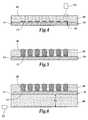
- the wafer 10is coated with a layer of epoxy 20 as depicted in FIG. 2.
- the epoxy 20may be applied using any of many semiconductor chip manufacturing techniques known in the art. Spraying, rolling or vapor deposition, for example, is used to apply the epoxy 20 to the wafer 10 .
- the epoxy 20may be non-conductive and may have a coefficient of thermal expansion similar to the wafer 10 .
- the epoxy 20may also be able to withstand the heat required to re-flow solder or other conductive material that is applied to the wafer 10 in subsequent processes.
- An epoxy material suitable for underfill, for example,may be used.
- the epoxy 20should be applied or deposited to a height that exceeds the upper surface of the RDL pads 13 by at least the diameter of the RDL pads 13 .
- the epoxy 20is then cured as required by the particular properties of the epoxy 20 .
- Some curing methodsmay include infrared heat or chemical processes, for example.
- the cured epoxy 20may have a relatively rough or undulating surface, as best seen in FIG. 3A. However, a desirable minimum thickness is one that extends past the upper surface of the RDL pads 13 by approximately the diameter of the RDL pads 13 .
- FIG. 3Bdepict a trimming process that may vaporize the top of the epoxy 20 to achieve a very flat surface and controlled height.
- An exaggerated surface of the epoxy 20is shown in FIG. 3A.
- the thinnest point of the epoxy 20should be approximately at least as thick as the diameter 34 of the RDL pad 13 plus the height of the RDL pad 13 .
- a controllermay be used to operate a laser 25 to vaporize selected areas of the epoxy 20 .
- the controllermay be the type of controller utilized for computer-numerical-control (CNC) machining, which maneuvers and operates a tool in three dimensions.
- CNCcomputer-numerical-control
- the controllermaneuvers the laser 25 about the wafer 10 and selectively vaporizes portions of the epoxy 20 .
- the process of removing the epoxy 20will be described in further detail below.
- the laser 25may be aimed at initial elevation 31 and generally parallel to the surface of the wafer 10 .
- This initial elevation 31 of the laser 25may be slightly above the highest point of the epoxy 30 .
- the controllerbegins sweeping the laser 25 across the wafer 10 and slowly lowers the laser 25 through excess epoxy 30 to final elevation 32 .
- the laser 25impinges on high points of the surface of the epoxy 20 and vaporizes the excess epoxy 30 as the laser 25 sweeps across the entire wafer 10 .
- the elevation 32is at a point where the distance 33 between the surface of the epoxy 20 and the surface of the RDL pads 13 is approximately the diameter 34 of the RDL pads 13 .
- the distance 33may be varied to optimize the aspect ratio for conductor screening, which will be described below.
- the laser 25may also be used to create openings 40 , the locations of which are represent by dashed lines, in the epoxy 20 as depicted in FIG. 4.
- the laser 25is first oriented to the wafer 10 using alignment marks 35 on the wafer 10 . If the alignment marks 35 have been covered during the epoxy coating process, a rough alignment can be made using a flat spot or other reference point on the wafer 10 .
- the laser 25may be used to etch away the epoxy 20 around the alignment marks 35 . After the alignment marks 35 are located, the location of RDL pads 13 can be very accurately determined by using the alignment marks 35 in conjunction with a coordinate map of the RDL pads 13 .
- the laser 25creates the openings 40 by vaporizing the epoxy 30 .
- the laser 25vaporizes the epoxy 20 down to the surface of the RDL pads 13 but does not affect the RDL pads 13 because of the reflective properties of the RDL pads 13 .
- This processis similar to using the laser 25 as a drill.
- the controllerdetermines drilling locations, which are generally above the RDL pads 13 , by moving the laser 25 relative to the alignment marks 35 .
- the laser 25may then be activated to vaporize the epoxy 20 and “drill” the openings 40 .
- the RDL pads 13act as “drill stops” because the RDL pads 13 reflect the laser 25 instead of being vaporized by the laser 25 .
- FIG. 5shows the openings 40 filled with a conductive material by screening, for example, to form interposer pads 50 .
- the aspect ratio of the openings 40may be adjusted so that the conductive material easily flows into the openings 40 and adequately fills the openings without leaving any voids. Also, the aspect ratio facilitates the conductive material filling the openings 40 and contacting the RDL pads 13 .
- the conductive materialmay be solder, conductive polymer or any other suitable material and may be screened into the openings 40 .
- the conductive materialforms a permanent and reliable electrical connection to RDL pads 13 . After screening into the openings 40 , the conductive material is re-flowed or cured.
- the wafer-interposerAfter re-flowing or curing, the wafer-interposer is at minimum thickness. If a thicker package is required or if it is desirable to protect the backside of the die 11 , then an epoxy coat can be applied to the back of the wafer 10 , as best seen in FIG. 6.
- the interposer pads 50may be used as contacts for testing and burn-in of the wafer 10 .
- the interposer pads 50may also be used to connect and attach the resulting device to a printed circuit board or other structure after the interposer is diced into individual circuits.
- FIG. 6depicts the wafer-interposer having an additional layer of epoxy 60 , which may be added to the backside of the wafer 10 .
- the technique for applying the epoxy 60 , the composition of the epoxy 60 and the method for creating a dimensionally precise surfaceis similar to the process for the front side of the wafer 10 , which has been described above.
- the thickness 61 of the wafer-interposermay be adjusted by removing and leveling the epoxy 60 using the laser 25 . Because there are no electrical contacts on the backside of the wafer 10 , the thickness 61 may be adjusted without concern for maintaining a particular aspect ratio. After construction of the wafer-interposer is complete, testing and burn-in may be performed while all circuits are in wafer form. After final testing, the wafer-interposer may be diced into individual components.
Landscapes
- Engineering & Computer Science (AREA)
- Computer Hardware Design (AREA)
- Microelectronics & Electronic Packaging (AREA)
- Power Engineering (AREA)
- Manufacturing & Machinery (AREA)
- Physics & Mathematics (AREA)
- Condensed Matter Physics & Semiconductors (AREA)
- General Physics & Mathematics (AREA)
- Testing Or Measuring Of Semiconductors Or The Like (AREA)
- Wire Bonding (AREA)
- Laser Beam Processing (AREA)
Abstract
Description
- This is a divisional application of co-pending application Ser. No. 09/738,228, entitled Method for Building an Interposer onto a Semiconductor Wafer Using Laser Techniques, filed on Dec. 15, 2000 in the name of John L. Pierce.[0001]
- The present invention relates generally to the field of integrated circuits, and more particularly, to a wafer interposer assembly and a system for building the same.[0002]
- Without limiting the scope of the invention, this background of the present invention will be described with reference to building a semiconductor wafer-interposer, as an example. After the introduction of the integrated circuit, engineers have worked diligently to produce electronic devices that are smaller and more functional than the previous versions of the devices. Advances in manufacturing techniques allow more components to be integrated into a smaller semiconductor die. More components within the die enable engineers to design devices having greater efficiency and more convenient functions. However, increasing the number of components within the die can adversely affect the size and manufacturing costs of the device.[0003]
- Each new device design often requires smaller, more efficient semiconductor packages to perform advanced functions and consume less power and space. Die size and number of contact pads influence the size of a semiconductor package. More components within the die require more contact pads, which facilitate electrical connections or interfaces between the die to other systems in the device. However, traditional connection techniques are not very space efficient.[0004]
- Traditionally, die design was limited because all connections between the components of the die interfacing systems were through the peripheral edges of the chip (for wire bonding) or through a standard pin or pad layout defined by a standardization body, such as the Joint Electrical Dimensional Electronic Committee (JEDEC). The interconnection requirements, therefore, have traditionally driven the die layout.[0005]
- Although space efficiency may be improved by using a semiconductor wafer-interposer, it is difficult to attached a separate interposer to a semiconductor wafer and maintain close dimensional tolerances. Close tolerance for package height is a requirement for many applications. Typically, thick packages are more reliable and have lower manufacturing costs. In contrast, thin packages may be required for applications where space and weight are at a premium. Additionally, manufacturing a thin package is usually costly because smaller components are more difficult to process and require more precise machinery.[0006]
- Current manufacturing processes cannot precisely and efficiently control the final height of the package. After the wafer-interposer assembly is diced, the footprint of the resulting semiconductor package is almost the size of the die, which is as small as the package can be without making a smaller die. However, the height of the package cannot be as accurately controlled because it varies according to the method used to construct the wafer-interposer.[0007]
- Another costly manufacturing process associated with assembling semiconductor packages having interposers is aligning the die with the interposer. The contact pads on the die and the interposer must be aligned and connected to result in a functional semiconductor package. Aligning minute contacts between the die and interposer is an expensive and time intensive process. Current available methods of alignment slow the manufacturing process and increase costs.[0008]
- Accordingly, there is a need for a system, method and apparatus for building a semiconductor wafer-interposer assembly that overcomes the present manufacturing limitations and inefficiencies.[0009]
- The present invention overcomes the existing manufacturing limitations and inefficiencies in the art by providing a wafer interposer assembly and system for building the same. The wafer interposer assembly includes a semiconductor wafer having a die and a redistribution layer pad, electrically connected to the die. An epoxy layer is deposited on the surface of the redistribution layer pad and the die. An opening is positioned through the epoxy layer and an interposer pad is positioned in the opening in electrical contact with the redistribution layerpad.[0010]
- In one embodiment, the semiconductor wafer of the wafer interposer assembly includes a plurality of die. The redistribution layer pad may comprise a material reflective to laser frequencies, a material compatible with solder, or a material compatible with conductive polymer. The epoxy layer may be disposed on the surface by a deposition process selected from the group consisting of spraying, rolling and vapor deposition. Moreover, the epoxy layer may comprise a nonconductive material having a coefficient of thermal expansion similar to the wafer. The height of the cured epoxy layer may be at least the length of the redistribution layer pad. The curing may involve a processes selected from the group consisting of heat processes and chemical processes. The epoxy layer is trimmed by a laser process to achieve a flat surface and controlled height. Additionally, the interposer pad may comprise a conductive material that is positioned in the opening which may be formed by a laser process. An epoxy coat is disposed on a backside of the wafer.[0011]
- In another aspect, the present invention is directed to a system for building a wafer interposer assembly. A depositor deposits an epoxy layer onto the surface of a semiconductor wafer having a plurality of die and a plurality of redistribution layer pads electrically connected to each die. A laser operates relative to the semiconductor wafer to trim the epoxy layer to a flat surface and controlled height and to bore a plurality of openings in alignment with the redistribution layer pads through the epoxy layer. A screener screens an interposer pad into the openings and into electrical contact with the redistribution layer pads.[0012]
- In one embodiment, the depositor is selected from the group consisting of spraying depositors, rolling depositors and vapor depositors. The laser may operate under the control of a controller that comprises a computer-numerical-control machine that maneuvers and operates the laser in three dimensions. A curing means employing a heat process or chemical process may be employed for curing the epoxy layer. The screener may screen a conductive material into the openings to form the interposer pads. An alignment mark may be position on the semiconductor wafer to provide orientation to the laser. Additionally, the depositor may deposit an epoxy coat on the backside of the semiconductor wafer and the laser may adjust the height of the epoxy coat.[0013]
- The above and further advantages of the invention may be better understood by referring to the following description in conjunction with the accompanying drawings in which corresponding numerals in the different figures refer to corresponding parts and in which:[0014]
- FIG. 1A is a perspective view of a semiconductor wafer in accordance with certain embodiments of the present invention;[0015]
- FIG. 1B is a cross-sectional view of the semiconductor wafer of FIG. 1A taken along[0016]
line 1B-1B. - FIG. 2 is a cross-sectional view of a wafer-interposer assembly in accordance with certain embodiments of the present invention;[0017]
- FIG. 3A is a cross-sectional view of a wafer-interposer assembly in accordance with certain embodiments of the present invention;[0018]
- FIG. 3B is a cross-sectional view of a wafer-interposer assembly in accordance with certain embodiments of the present invention;[0019]
- FIG. 4 is a cross-sectional view of a wafer-interposer assembly in accordance with certain embodiments of the present invention;[0020]
- FIG. 5 is a cross-sectional view of a wafer-interposer assembly in accordance with certain embodiments of the present invention; and[0021]
- FIG. 6 is a cross-sectional view of a wafer-interposer assembly in accordance with certain embodiments of the present invention.[0022]
- Although making and using various embodiments of the present invention are discussed herein in terms of using laser techniques to build an interposer onto a wafer, it should be appreciated that the present invention provides many applicable inventive concepts that can be embodied in a wide variety of specific contexts. The specific embodiments discussed herein are merely illustrative of specific ways to make and use the invention and do not limit the scope of the invention.[0023]
- Interposers allow greater freedom to die designers because the layout of a die and its contact pads can be defined according to the interaction of the functional elements of the die rather than according to the standardization requirements. The interposer can be designed with a standardized layout of contact pads on its upper surface and can electrically connect each die pad to a corresponding interposer contact pad without an interposer pad being directly above its corresponding die pad. Not only does the interposer provide for standardized interconnection, it also provides for the use of standard test hardware, software, cabling and connectors compatible with existing industry infrastructure.[0024]
- An additional advantage of the interposer is that more than one interposer can be designed for each wafer. A manufacturer can then, by substituting a different interposer, modify the layout of the interposer pads to conform to a different layout or packaging standard. Alternatively, if the die and interposer are designed for modularity, a single interposer design may be useful on more than one chip design. A specific interposer design will typically be necessary for each unique die design.[0025]
- FIG. 1A depicts a[0026]
semiconductor wafer 10 having a plurality of die including adie 11, which may have many circuits within its structure. Referring now to FIG. 1A and FIG. 1B, which is a cross-sectional view of FIG. 1A alongline 1B-1B, thewafer 10 may have several identical ordifferent dice 11, which eventually may be separated or diced into individual semiconductor chips. For clarity of illustration, dashed lines are used to represent the kerfs betweendie 11. One or moredie pads 12 electrically contact the circuits withindie 11. An underbump metalization may be deposited onto thedie pads 12. A redistribution layer (RDL) may then be deposited onto thewafer 10. One or more known semiconductor processes, such as photolithography or etching for example, may be used to process the RDL intoRDL pads 13. TheRDL pads 13 may then be connected to thedie pads 12 byconnectors 14. TheRDL pads 13 provide an interface between the circuits of thedie 11 and an interposer. Each of thedie pads 12 corresponds to aparticular RDL pad 13. - The[0027]
RDL pads 13 may be a material that is reflective to laser frequencies to facilitate subsequent processes of the present invention. TheRDL pads 13 may also be made from a material that is compatible with solder or conductive polymer. Copper, for example, may be one suitable material forRDL pads 13. Other materials that are electrically conductive and compatible with solder or conductive polymers may also be used for theRDL pads 13 and will be apparent to those having ordinary skill in the art. - The layout and size of the[0028]
RDL pads 13 may have the same configuration as the pad configuration of a finished semiconductor package. Designing the configuration of theRDL pads 13 to match the requirements of the finished package increases manufacturing efficiency. Multiple,identical dice 11 may be efficiently produced in large quantities and used in a variety of different applications by simply changing the configuration of theRDL pads 13. Efficiency increases because thesame die 11 may be used for multiple applications that require different semiconductor package configurations. - Next, the[0029]
wafer 10 is coated with a layer ofepoxy 20 as depicted in FIG. 2. The epoxy20 may be applied using any of many semiconductor chip manufacturing techniques known in the art. Spraying, rolling or vapor deposition, for example, is used to apply the epoxy20 to thewafer 10. The epoxy20 may be non-conductive and may have a coefficient of thermal expansion similar to thewafer 10. The epoxy20 may also be able to withstand the heat required to re-flow solder or other conductive material that is applied to thewafer 10 in subsequent processes. An epoxy material suitable for underfill, for example, may be used. - The epoxy[0030]20 should be applied or deposited to a height that exceeds the upper surface of the
RDL pads 13 by at least the diameter of theRDL pads 13. The epoxy20 is then cured as required by the particular properties of the epoxy20. Some curing methods may include infrared heat or chemical processes, for example. The curedepoxy 20 may have a relatively rough or undulating surface, as best seen in FIG. 3A. However, a desirable minimum thickness is one that extends past the upper surface of theRDL pads 13 by approximately the diameter of theRDL pads 13. - FIG. 3B depict a trimming process that may vaporize the top of the epoxy[0031]20 to achieve a very flat surface and controlled height. An exaggerated surface of the epoxy20 is shown in FIG. 3A. The thinnest point of the epoxy20 should be approximately at least as thick as the
diameter 34 of theRDL pad 13 plus the height of theRDL pad 13. - A controller (not shown) may be used to operate a[0032]
laser 25 to vaporize selected areas of the epoxy20. The controller, for example, may be the type of controller utilized for computer-numerical-control (CNC) machining, which maneuvers and operates a tool in three dimensions. In this particular application, the controller maneuvers thelaser 25 about thewafer 10 and selectively vaporizes portions of the epoxy20. The process of removing the epoxy20 will be described in further detail below. - In FIG. 3B, the[0033]
laser 25 may be aimed atinitial elevation 31 and generally parallel to the surface of thewafer 10. Thisinitial elevation 31 of thelaser 25 may be slightly above the highest point of the epoxy30. The controller begins sweeping thelaser 25 across thewafer 10 and slowly lowers thelaser 25 throughexcess epoxy 30 tofinal elevation 32. As it is lowered, thelaser 25 impinges on high points of the surface of the epoxy20 and vaporizes theexcess epoxy 30 as thelaser 25 sweeps across theentire wafer 10. Theelevation 32 is at a point where thedistance 33 between the surface of the epoxy20 and the surface of theRDL pads 13 is approximately thediameter 34 of theRDL pads 13. Thedistance 33 may be varied to optimize the aspect ratio for conductor screening, which will be described below. - Once the epoxy[0034]20 is planarized, the
laser 25 may also be used to createopenings 40, the locations of which are represent by dashed lines, in the epoxy20 as depicted in FIG. 4. Thelaser 25 is first oriented to thewafer 10 using alignment marks35 on thewafer 10. If the alignment marks35 have been covered during the epoxy coating process, a rough alignment can be made using a flat spot or other reference point on thewafer 10. Next, thelaser 25 may be used to etch away the epoxy20 around the alignment marks35. After the alignment marks35 are located, the location ofRDL pads 13 can be very accurately determined by using the alignment marks35 in conjunction with a coordinate map of theRDL pads 13. Thelaser 25 creates theopenings 40 by vaporizing theepoxy 30. Thelaser 25 vaporizes the epoxy20 down to the surface of theRDL pads 13 but does not affect theRDL pads 13 because of the reflective properties of theRDL pads 13. - This process is similar to using the[0035]
laser 25 as a drill. The controller determines drilling locations, which are generally above theRDL pads 13, by moving thelaser 25 relative to the alignment marks35. Thelaser 25 may then be activated to vaporize the epoxy20 and “drill” theopenings 40. TheRDL pads 13 act as “drill stops” because theRDL pads 13 reflect thelaser 25 instead of being vaporized by thelaser 25. - FIG. 5 shows the[0036]
openings 40 filled with a conductive material by screening, for example, to form interposer pads50. The aspect ratio of theopenings 40 may be adjusted so that the conductive material easily flows into theopenings 40 and adequately fills the openings without leaving any voids. Also, the aspect ratio facilitates the conductive material filling theopenings 40 and contacting theRDL pads 13. The conductive material may be solder, conductive polymer or any other suitable material and may be screened into theopenings 40. The conductive material forms a permanent and reliable electrical connection toRDL pads 13. After screening into theopenings 40, the conductive material is re-flowed or cured. After re-flowing or curing, the wafer-interposer is at minimum thickness. If a thicker package is required or if it is desirable to protect the backside of the die11, then an epoxy coat can be applied to the back of thewafer 10, as best seen in FIG. 6. - The interposer pads[0037]50 may be used as contacts for testing and burn-in of the
wafer 10. The interposer pads50 may also be used to connect and attach the resulting device to a printed circuit board or other structure after the interposer is diced into individual circuits. - FIG. 6 depicts the wafer-interposer having an additional layer of[0038]
epoxy 60, which may be added to the backside of thewafer 10. The technique for applying the epoxy60, the composition of the epoxy60 and the method for creating a dimensionally precise surface is similar to the process for the front side of thewafer 10, which has been described above. Thethickness 61 of the wafer-interposer may be adjusted by removing and leveling the epoxy60 using thelaser 25. Because there are no electrical contacts on the backside of thewafer 10, thethickness 61 may be adjusted without concern for maintaining a particular aspect ratio. After construction of the wafer-interposer is complete, testing and burn-in may be performed while all circuits are in wafer form. After final testing, the wafer-interposer may be diced into individual components. - While specific alternatives to steps of the invention have been described herein, additional alternatives not specifically disclosed but known in the art are intended to fall within the scope of the invention. Thus, it is understood that other applications of the present invention will be apparent to those skilled in the art upon the reading of the described embodiment and a consideration of the appended claims and drawings.[0039]
Claims (30)
Priority Applications (1)
| Application Number | Priority Date | Filing Date | Title |
|---|---|---|---|
| US10/373,413US6933617B2 (en) | 2000-12-15 | 2003-02-24 | Wafer interposer assembly |
Applications Claiming Priority (2)
| Application Number | Priority Date | Filing Date | Title |
|---|---|---|---|
| US09/738,228US6524885B2 (en) | 2000-12-15 | 2000-12-15 | Method, apparatus and system for building an interposer onto a semiconductor wafer using laser techniques |
| US10/373,413US6933617B2 (en) | 2000-12-15 | 2003-02-24 | Wafer interposer assembly |
Related Parent Applications (1)
| Application Number | Title | Priority Date | Filing Date |
|---|---|---|---|
| US09/738,228DivisionUS6524885B2 (en) | 2000-12-15 | 2000-12-15 | Method, apparatus and system for building an interposer onto a semiconductor wafer using laser techniques |
Publications (2)
| Publication Number | Publication Date |
|---|---|
| US20030148108A1true US20030148108A1 (en) | 2003-08-07 |
| US6933617B2 US6933617B2 (en) | 2005-08-23 |
Family
ID=24967115
Family Applications (2)
| Application Number | Title | Priority Date | Filing Date |
|---|---|---|---|
| US09/738,228Expired - Fee RelatedUS6524885B2 (en) | 2000-12-15 | 2000-12-15 | Method, apparatus and system for building an interposer onto a semiconductor wafer using laser techniques |
| US10/373,413Expired - LifetimeUS6933617B2 (en) | 2000-12-15 | 2003-02-24 | Wafer interposer assembly |
Family Applications Before (1)
| Application Number | Title | Priority Date | Filing Date |
|---|---|---|---|
| US09/738,228Expired - Fee RelatedUS6524885B2 (en) | 2000-12-15 | 2000-12-15 | Method, apparatus and system for building an interposer onto a semiconductor wafer using laser techniques |
Country Status (1)
| Country | Link |
|---|---|
| US (2) | US6524885B2 (en) |
Cited By (1)
| Publication number | Priority date | Publication date | Assignee | Title |
|---|---|---|---|---|
| US20040212053A1 (en)* | 2003-04-28 | 2004-10-28 | Koh Wei H. | Semiconductor package for random access memory integrated circuits |
Families Citing this family (40)
| Publication number | Priority date | Publication date | Assignee | Title |
|---|---|---|---|---|
| US6392428B1 (en) | 1999-11-16 | 2002-05-21 | Eaglestone Partners I, Llc | Wafer level interposer |
| US6537831B1 (en) | 2000-07-31 | 2003-03-25 | Eaglestone Partners I, Llc | Method for selecting components for a matched set using a multi wafer interposer |
| US6812048B1 (en)* | 2000-07-31 | 2004-11-02 | Eaglestone Partners I, Llc | Method for manufacturing a wafer-interposer assembly |
| US6815712B1 (en) | 2000-10-02 | 2004-11-09 | Eaglestone Partners I, Llc | Method for selecting components for a matched set from a wafer-interposer assembly |
| US6686657B1 (en)* | 2000-11-07 | 2004-02-03 | Eaglestone Partners I, Llc | Interposer for improved handling of semiconductor wafers and method of use of same |
| US6529022B2 (en)* | 2000-12-15 | 2003-03-04 | Eaglestone Pareners I, Llc | Wafer testing interposer for a conventional package |
| US6524885B2 (en) | 2000-12-15 | 2003-02-25 | Eaglestone Partners I, Llc | Method, apparatus and system for building an interposer onto a semiconductor wafer using laser techniques |
| US6673653B2 (en) | 2001-02-23 | 2004-01-06 | Eaglestone Partners I, Llc | Wafer-interposer using a ceramic substrate |
| TWI232560B (en)* | 2002-04-23 | 2005-05-11 | Sanyo Electric Co | Semiconductor device and its manufacture |
| TWI229435B (en)* | 2002-06-18 | 2005-03-11 | Sanyo Electric Co | Manufacture of semiconductor device |
| TWI227550B (en)* | 2002-10-30 | 2005-02-01 | Sanyo Electric Co | Semiconductor device manufacturing method |
| US7723210B2 (en) | 2002-11-08 | 2010-05-25 | Amkor Technology, Inc. | Direct-write wafer level chip scale package |
| US7361533B1 (en) | 2002-11-08 | 2008-04-22 | Amkor Technology, Inc. | Stacked embedded leadframe |
| US6905914B1 (en) | 2002-11-08 | 2005-06-14 | Amkor Technology, Inc. | Wafer level package and fabrication method |
| JP4401181B2 (en)* | 2003-08-06 | 2010-01-20 | 三洋電機株式会社 | Semiconductor device and manufacturing method thereof |
| TWI221343B (en)* | 2003-10-21 | 2004-09-21 | Advanced Semiconductor Eng | Wafer structure for preventing contamination of bond pads during SMT process and process for the same |
| US8399291B2 (en)* | 2005-06-29 | 2013-03-19 | Intel Corporation | Underfill device and method |
| US7572681B1 (en) | 2005-12-08 | 2009-08-11 | Amkor Technology, Inc. | Embedded electronic component package |
| TWI324800B (en)* | 2005-12-28 | 2010-05-11 | Sanyo Electric Co | Method for manufacturing semiconductor device |
| US7902660B1 (en) | 2006-05-24 | 2011-03-08 | Amkor Technology, Inc. | Substrate for semiconductor device and manufacturing method thereof |
| US8796561B1 (en) | 2009-10-05 | 2014-08-05 | Amkor Technology, Inc. | Fan out build up substrate stackable package and method |
| US8937381B1 (en) | 2009-12-03 | 2015-01-20 | Amkor Technology, Inc. | Thin stackable package and method |
| US9691734B1 (en) | 2009-12-07 | 2017-06-27 | Amkor Technology, Inc. | Method of forming a plurality of electronic component packages |
| TWI419302B (en)* | 2010-02-11 | 2013-12-11 | Advanced Semiconductor Eng | Package process |
| US8324511B1 (en) | 2010-04-06 | 2012-12-04 | Amkor Technology, Inc. | Through via nub reveal method and structure |
| US8294276B1 (en) | 2010-05-27 | 2012-10-23 | Amkor Technology, Inc. | Semiconductor device and fabricating method thereof |
| US8440554B1 (en) | 2010-08-02 | 2013-05-14 | Amkor Technology, Inc. | Through via connected backside embedded circuit features structure and method |
| US8487445B1 (en) | 2010-10-05 | 2013-07-16 | Amkor Technology, Inc. | Semiconductor device having through electrodes protruding from dielectric layer |
| US8791501B1 (en) | 2010-12-03 | 2014-07-29 | Amkor Technology, Inc. | Integrated passive device structure and method |
| US8390130B1 (en) | 2011-01-06 | 2013-03-05 | Amkor Technology, Inc. | Through via recessed reveal structure and method |
| US20120206892A1 (en)* | 2011-02-10 | 2012-08-16 | Apple Inc. | Circular interposers |
| US9474156B2 (en)* | 2011-02-10 | 2016-10-18 | Apple Inc. | Interposer connectors with alignment features |
| EP2503621A1 (en)* | 2011-03-24 | 2012-09-26 | Moser Baer India Ltd. | A barrier layer and a method of manufacturing the barrier layer |
| US9033740B2 (en) | 2011-04-25 | 2015-05-19 | Apple Inc. | Interposer connectors |
| US8791536B2 (en) | 2011-04-28 | 2014-07-29 | Aptina Imaging Corporation | Stacked sensor packaging structure and method |
| US8552548B1 (en) | 2011-11-29 | 2013-10-08 | Amkor Technology, Inc. | Conductive pad on protruding through electrode semiconductor device |
| US9048298B1 (en) | 2012-03-29 | 2015-06-02 | Amkor Technology, Inc. | Backside warpage control structure and fabrication method |
| US9129943B1 (en) | 2012-03-29 | 2015-09-08 | Amkor Technology, Inc. | Embedded component package and fabrication method |
| US9041840B2 (en) | 2012-08-21 | 2015-05-26 | Semiconductor Components Industries, Llc | Backside illuminated image sensors with stacked dies |
| US9978702B2 (en)* | 2016-05-11 | 2018-05-22 | RGD Circuts, Inc. | Resurfaceable contact pad for silicon or organic redistribution interposer for semiconductor probing |
Citations (93)
| Publication number | Priority date | Publication date | Assignee | Title |
|---|---|---|---|---|
| US3939588A (en)* | 1974-06-24 | 1976-02-24 | Hockaday Robert C | Lettering guide apparatus |
| US4577214A (en)* | 1981-05-06 | 1986-03-18 | At&T Bell Laboratories | Low-inductance power/ground distribution in a package for a semiconductor chip |
| US4617730A (en)* | 1984-08-13 | 1986-10-21 | International Business Machines Corporation | Method of fabricating a chip interposer |
| US4628411A (en)* | 1984-03-12 | 1986-12-09 | International Business Machines Corporation | Apparatus for directly powering a multi-chip module from a power distribution bus |
| US4688151A (en)* | 1986-03-10 | 1987-08-18 | International Business Machines Corporation | Multilayered interposer board for powering high current chip modules |
| US4868712A (en)* | 1987-02-04 | 1989-09-19 | Woodman John K | Three dimensional integrated circuit package |
| US4998885A (en)* | 1989-10-27 | 1991-03-12 | International Business Machines Corporation | Elastomeric area array interposer |
| US5016138A (en)* | 1987-10-27 | 1991-05-14 | Woodman John K | Three dimensional integrated circuit package |
| US5060052A (en)* | 1990-09-04 | 1991-10-22 | Motorola, Inc. | TAB bonded semiconductor device having off-chip power and ground distribution |
| US5065227A (en)* | 1990-06-04 | 1991-11-12 | International Business Machines Corporation | Integrated circuit packaging using flexible substrate |
| US5068558A (en)* | 1988-10-07 | 1991-11-26 | Nippon Ferrofluidics Corporation | Magnetic bearing device |
| US5123850A (en)* | 1990-04-06 | 1992-06-23 | Texas Instruments Incorporated | Non-destructive burn-in test socket for integrated circuit die |
| US5132613A (en)* | 1990-11-30 | 1992-07-21 | International Business Machines Corporation | Low inductance side mount decoupling test structure |
| US5148266A (en)* | 1990-09-24 | 1992-09-15 | Ist Associates, Inc. | Semiconductor chip assemblies having interposer and flexible lead |
| US5148265A (en)* | 1990-09-24 | 1992-09-15 | Ist Associates, Inc. | Semiconductor chip assemblies with fan-in leads |
| US5309021A (en)* | 1991-10-16 | 1994-05-03 | Mitsubishi Denki Kabushiki Kaisha | Semiconductor device having particular power distribution interconnection arrangement |
| US5327325A (en)* | 1993-02-08 | 1994-07-05 | Fairchild Space And Defense Corporation | Three-dimensional integrated circuit package |
| US5347162A (en)* | 1989-08-28 | 1994-09-13 | Lsi Logic Corporation | Preformed planar structures employing embedded conductors |
| US5371654A (en)* | 1992-10-19 | 1994-12-06 | International Business Machines Corporation | Three dimensional high performance interconnection package |
| US5382898A (en)* | 1992-09-21 | 1995-01-17 | Cerprobe Corporation | High density probe card for testing electrical circuits |
| US5384691A (en)* | 1993-01-08 | 1995-01-24 | General Electric Company | High density interconnect multi-chip modules including embedded distributed power supply elements |
| US5394303A (en)* | 1992-09-11 | 1995-02-28 | Kabushiki Kaisha Toshiba | Semiconductor device |
| US5399505A (en)* | 1993-07-23 | 1995-03-21 | Motorola, Inc. | Method and apparatus for performing wafer level testing of integrated circuit dice |
| US5399898A (en)* | 1992-07-17 | 1995-03-21 | Lsi Logic Corporation | Multi-chip semiconductor arrangements using flip chip dies |
| US5410259A (en)* | 1992-06-01 | 1995-04-25 | Tokyo Electron Yamanashi Limited | Probing device setting a probe card parallel |
| US5476211A (en)* | 1993-11-16 | 1995-12-19 | Form Factor, Inc. | Method of manufacturing electrical contacts, using a sacrificial member |
| US5477160A (en)* | 1992-08-12 | 1995-12-19 | Fujitsu Limited | Module test card |
| US5483421A (en)* | 1992-03-09 | 1996-01-09 | International Business Machines Corporation | IC chip attachment |
| US5489804A (en)* | 1989-08-28 | 1996-02-06 | Lsi Logic Corporation | Flexible preformed planar structures for interposing between a chip and a substrate |
| US5491612A (en)* | 1995-02-21 | 1996-02-13 | Fairchild Space And Defense Corporation | Three-dimensional modular assembly of integrated circuits |
| US5497079A (en)* | 1992-09-01 | 1996-03-05 | Matsushita Electric Industrial Co., Ltd. | Semiconductor testing apparatus, semiconductor testing circuit chip, and probe card |
| US5517515A (en)* | 1994-08-17 | 1996-05-14 | International Business Machines Corporation | Multichip module with integrated test circuitry disposed within interposer substrate |
| US5518964A (en)* | 1994-07-07 | 1996-05-21 | Tessera, Inc. | Microelectronic mounting with multiple lead deformation and bonding |
| US5532612A (en)* | 1994-07-19 | 1996-07-02 | Liang; Louis H. | Methods and apparatus for test and burn-in of integrated circuit devices |
| US5532610A (en)* | 1993-08-25 | 1996-07-02 | Nec Corporation | Apparatus for testing semicondctor wafer |
| US5544017A (en)* | 1992-08-05 | 1996-08-06 | Fujitsu Limited | Multichip module substrate |
| US5570032A (en)* | 1993-08-17 | 1996-10-29 | Micron Technology, Inc. | Wafer scale burn-in apparatus and process |
| US5579207A (en)* | 1994-10-20 | 1996-11-26 | Hughes Electronics | Three-dimensional integrated circuit stacking |
| US5594273A (en)* | 1993-07-23 | 1997-01-14 | Motorola Inc. | Apparatus for performing wafer-level testing of integrated circuits where test pads lie within integrated circuit die but overly no active circuitry for improved yield |
| US5600541A (en)* | 1993-12-08 | 1997-02-04 | Hughes Aircraft Company | Vertical IC chip stack with discrete chip carriers formed from dielectric tape |
| US5600257A (en)* | 1995-08-09 | 1997-02-04 | International Business Machines Corporation | Semiconductor wafer test and burn-in |
| US5612575A (en)* | 1994-05-20 | 1997-03-18 | Matra Marconi Space France | Method of connecting the output pads on an integrated circuit chip, and multichip module thus obtained |
| US5615089A (en)* | 1994-07-26 | 1997-03-25 | Fujitsu Limited | BGA semiconductor device including a plurality of semiconductor chips located on upper and lower surfaces of a first substrate |
| US5635101A (en)* | 1996-01-22 | 1997-06-03 | Janke George A | Deicing composition and method |
| US5637920A (en)* | 1995-10-04 | 1997-06-10 | Lsi Logic Corporation | High contact density ball grid array package for flip-chips |
| US5654588A (en)* | 1993-07-23 | 1997-08-05 | Motorola Inc. | Apparatus for performing wafer-level testing of integrated circuits where the wafer uses a segmented conductive top-layer bus structure |
| US5655290A (en)* | 1992-08-05 | 1997-08-12 | Fujitsu Limited | Method for making a three-dimensional multichip module |
| US5685885A (en)* | 1990-09-24 | 1997-11-11 | Tessera, Inc. | Wafer-scale techniques for fabrication of semiconductor chip assemblies |
| US5701666A (en)* | 1994-08-31 | 1997-12-30 | Motorola, Inc. | Method for manufacturing a stimulus wafer for use in a wafer-to-wafer testing system to test integrated circuits located on a product wafer |
| US5710071A (en)* | 1995-12-04 | 1998-01-20 | Motorola, Inc. | Process for underfilling a flip-chip semiconductor device |
| US5714800A (en)* | 1996-03-21 | 1998-02-03 | Motorola, Inc. | Integrated circuit assembly having a stepped interposer and method |
| US5759047A (en)* | 1996-05-24 | 1998-06-02 | International Business Machines Corporation | Flexible circuitized interposer with apertured member and method for making same |
| US5764655A (en)* | 1997-07-02 | 1998-06-09 | International Business Machines Corporation | Built in self test with memory |
| US5764071A (en)* | 1996-01-05 | 1998-06-09 | International Business Machines Corporation | Method and system for testing an electronic module mounted on a printed circuit board |
| US5789807A (en)* | 1996-10-15 | 1998-08-04 | International Business Machines Corporation | On-chip power distribution for improved decoupling |
| US5794175A (en)* | 1997-09-09 | 1998-08-11 | Teradyne, Inc. | Low cost, highly parallel memory tester |
| US5796746A (en)* | 1995-12-22 | 1998-08-18 | Micron Technology, Inc. | Device and method for testing integrated circuit dice in an integrated circuit module |
| US5798652A (en)* | 1993-11-23 | 1998-08-25 | Semicoa Semiconductors | Method of batch testing surface mount devices using a substrate edge connector |
| US5800184A (en)* | 1994-03-08 | 1998-09-01 | International Business Machines Corporation | High density electrical interconnect apparatus and method |
| US5805422A (en)* | 1994-09-21 | 1998-09-08 | Nec Corporation | Semiconductor package with flexible board and method of fabricating the same |
| US5802713A (en)* | 1995-01-20 | 1998-09-08 | Fairchild Space And Defense Corportion | Circuit board manufacturing method |
| US5806181A (en)* | 1993-11-16 | 1998-09-15 | Formfactor, Inc. | Contact carriers (tiles) for populating larger substrates with spring contacts |
| US5834946A (en)* | 1995-10-19 | 1998-11-10 | Mosaid Technologies Incorporated | Integrated circuit test head |
| US5832601A (en)* | 1993-11-16 | 1998-11-10 | Form Factor, Inc. | Method of making temporary connections between electronic components |
| US5834844A (en)* | 1995-03-24 | 1998-11-10 | Shinko Electric Industries Co., Ltd. | Semiconductor device having an element with circuit pattern thereon |
| US5838072A (en)* | 1997-02-24 | 1998-11-17 | Mosel Vitalic Corporation | Intrachip power distribution package and method for semiconductors having a supply node electrically interconnected with one or more intermediate nodes |
| US5838060A (en)* | 1995-12-12 | 1998-11-17 | Comer; Alan E. | Stacked assemblies of semiconductor packages containing programmable interconnect |
| US5844803A (en)* | 1997-02-17 | 1998-12-01 | Micron Technology, Inc. | Method of sorting a group of integrated circuit devices for those devices requiring special testing |
| US5854507A (en)* | 1998-07-21 | 1998-12-29 | Hewlett-Packard Company | Multiple chip assembly |
| US5878486A (en)* | 1993-11-16 | 1999-03-09 | Formfactor, Inc. | Method of burning-in semiconductor devices |
| US5885849A (en)* | 1995-03-28 | 1999-03-23 | Tessera, Inc. | Methods of making microelectronic assemblies |
| US5892287A (en)* | 1997-08-18 | 1999-04-06 | Texas Instruments | Semiconductor device including stacked chips having metal patterned on circuit surface and on edge side of chip |
| US5897326A (en)* | 1993-11-16 | 1999-04-27 | Eldridge; Benjamin N. | Method of exercising semiconductor devices |
| US5900738A (en)* | 1993-11-16 | 1999-05-04 | Formfactor, Inc. | Contact structure device for interconnections, interposer, semiconductor assembly and package using the same and method |
| US5905382A (en)* | 1990-08-29 | 1999-05-18 | Micron Technology, Inc. | Universal wafer carrier for wafer level die burn-in |
| US5915752A (en)* | 1992-07-24 | 1999-06-29 | Tessera, Inc. | Method of making connections to a semiconductor chip assembly |
| US5927193A (en)* | 1997-10-16 | 1999-07-27 | International Business Machines Corporation | Process for via fill |
| US5949246A (en)* | 1997-01-28 | 1999-09-07 | International Business Machines | Test head for applying signals in a burn-in test of an integrated circuit |
| US6013944A (en)* | 1997-02-10 | 2000-01-11 | Fujitsu Limited | Semiconductor device in which chip electrodes are connected to terminals arranged along the periphery of an insulative board |
| US6018462A (en)* | 1997-06-30 | 2000-01-25 | Nec Corporation | Multi-tip module |
| US6161205A (en)* | 1992-11-20 | 2000-12-12 | Micron Technology, Inc. | Testing and burn-in of IC chips using radio frequency transmission |
| US6190940B1 (en)* | 1999-01-21 | 2001-02-20 | Lucent Technologies Inc. | Flip chip assembly of semiconductor IC chips |
| US6229216B1 (en)* | 1999-01-11 | 2001-05-08 | Intel Corporation | Silicon interposer and multi-chip-module (MCM) with through substrate vias |
| US6297553B1 (en)* | 1998-10-30 | 2001-10-02 | Shinko Electric Industries Co., Ltd | Semiconductor device and process for producing the same |
| US6331782B1 (en)* | 1998-03-23 | 2001-12-18 | Conexant Systems, Inc. | Method and apparatus for wireless testing of integrated circuits |
| US6376769B1 (en)* | 1999-05-18 | 2002-04-23 | Amerasia International Technology, Inc. | High-density electronic package, and method for making same |
| US6392428B1 (en)* | 1999-11-16 | 2002-05-21 | Eaglestone Partners I, Llc | Wafer level interposer |
| US6627998B1 (en)* | 2000-07-27 | 2003-09-30 | International Business Machines Corporation | Wafer scale thin film package |
| US6717819B1 (en)* | 1999-06-01 | 2004-04-06 | Amerasia International Technology, Inc. | Solderable flexible adhesive interposer as for an electronic package, and method for making same |
| US6759741B2 (en)* | 2000-07-31 | 2004-07-06 | Eaglestone Partners I, Llc | Matched set of integrated circuit chips selected from a multi wafer-interposer |
| US6812048B1 (en)* | 2000-07-31 | 2004-11-02 | Eaglestone Partners I, Llc | Method for manufacturing a wafer-interposer assembly |
| US6815712B1 (en)* | 2000-10-02 | 2004-11-09 | Eaglestone Partners I, Llc | Method for selecting components for a matched set from a wafer-interposer assembly |
| US6822469B1 (en)* | 2000-07-31 | 2004-11-23 | Eaglestone Partners I, Llc | Method for testing multiple semiconductor wafers |
Family Cites Families (51)
| Publication number | Priority date | Publication date | Assignee | Title |
|---|---|---|---|---|
| US5829128A (en) | 1993-11-16 | 1998-11-03 | Formfactor, Inc. | Method of mounting resilient contact structures to semiconductor devices |
| US5086558A (en) | 1990-09-13 | 1992-02-11 | International Business Machines Corporation | Direct attachment of semiconductor chips to a substrate with a substrate with a thermoplastic interposer |
| US6064213A (en) | 1993-11-16 | 2000-05-16 | Formfactor, Inc. | Wafer-level burn-in and test |
| US6246247B1 (en) | 1994-11-15 | 2001-06-12 | Formfactor, Inc. | Probe card assembly and kit, and methods of using same |
| US5657206A (en) | 1994-06-23 | 1997-08-12 | Cubic Memory, Inc. | Conductive epoxy flip-chip package and method |
| US5798286A (en) | 1995-09-22 | 1998-08-25 | Tessera, Inc. | Connecting multiple microelectronic elements with lead deformation |
| TW273635B (en) | 1994-09-01 | 1996-04-01 | Aesop | |
| JPH08236654A (en) | 1995-02-23 | 1996-09-13 | Matsushita Electric Ind Co Ltd | Chip carrier and manufacturing method thereof |
| US5635010A (en) | 1995-04-14 | 1997-06-03 | Pepe; Angel A. | Dry adhesive joining of layers of electronic devices |
| US5765279A (en) | 1995-05-22 | 1998-06-16 | Fujitsu Limited | Methods of manufacturing power supply distribution structures for multichip modules |
| US6046600A (en) | 1995-10-31 | 2000-04-04 | Texas Instruments Incorporated | Process of testing integrated circuit dies on a wafer |
| US5942246A (en) | 1996-02-16 | 1999-08-24 | The Liposome Company, Inc. | Etherlipid containing multiple lipid liposomes |
| US5936847A (en) | 1996-05-02 | 1999-08-10 | Hei, Inc. | Low profile electronic circuit modules |
| US5917242A (en) | 1996-05-20 | 1999-06-29 | Micron Technology, Inc. | Combination of semiconductor interconnect |
| EP2287897A3 (en) | 1996-05-27 | 2011-11-02 | Dai Nippon Printing Co., Ltd. | Circuit member for semiconductor device, semiconductor device using the same, and process for producing said circuit member and said semiconductor device |
| US6020220A (en) | 1996-07-09 | 2000-02-01 | Tessera, Inc. | Compliant semiconductor chip assemblies and methods of making same |
| US5748452A (en) | 1996-07-23 | 1998-05-05 | International Business Machines Corporation | Multi-electronic device package |
| US6050829A (en) | 1996-08-28 | 2000-04-18 | Formfactor, Inc. | Making discrete power connections to a space transformer of a probe card assembly |
| US5707881A (en) | 1996-09-03 | 1998-01-13 | Motorola, Inc. | Test structure and method for performing burn-in testing of a semiconductor product wafer |
| JP3604248B2 (en) | 1997-02-25 | 2004-12-22 | 沖電気工業株式会社 | Method for manufacturing semiconductor device |
| US5950070A (en) | 1997-05-15 | 1999-09-07 | Kulicke & Soffa Investments | Method of forming a chip scale package, and a tool used in forming the chip scale package |
| KR100278219B1 (en) | 1997-06-18 | 2001-01-15 | 클라크 3세 존 엠. | Method of making flip chip and bga interconnections |
| US6082610A (en) | 1997-06-23 | 2000-07-04 | Ford Motor Company | Method of forming interconnections on electronic modules |
| US6137299A (en) | 1997-06-27 | 2000-10-24 | International Business Machines Corporation | Method and apparatus for testing integrated circuit chips |
| JP3028791B2 (en) | 1997-08-06 | 2000-04-04 | 日本電気株式会社 | How to mount chip components |
| US6069026A (en) | 1997-08-18 | 2000-05-30 | Texas Instruments Incorporated | Semiconductor device and method of fabrication |
| US6080494A (en) | 1997-08-29 | 2000-06-27 | Texas Instruments Incorporated | Method to manufacture ball grid arrays with excellent solder ball adhesion for semiconductor packaging and the array |
| US6083773A (en) | 1997-09-16 | 2000-07-04 | Micron Technology, Inc. | Methods of forming flip chip bumps and related flip chip bump constructions |
| RU2133523C1 (en) | 1997-11-03 | 1999-07-20 | Закрытое акционерное общество "Техно-ТМ" | Three-dimensional electron module |
| US6002178A (en) | 1997-11-12 | 1999-12-14 | Lin; Paul T. | Multiple chip module configuration to simplify testing process and reuse of known-good chip-size package (CSP) |
| US6432744B1 (en) | 1997-11-20 | 2002-08-13 | Texas Instruments Incorporated | Wafer-scale assembly of chip-size packages |
| JP3188876B2 (en) | 1997-12-29 | 2001-07-16 | インターナショナル・ビジネス・マシーンズ・コーポレ−ション | Method, test head and test apparatus for testing product chip |
| EP1202348A3 (en) | 1998-06-04 | 2004-05-12 | Matsushita Electric Industrial Co., Ltd. | Semiconductor device and method of manufacturing same |
| US5977640A (en) | 1998-06-26 | 1999-11-02 | International Business Machines Corporation | Highly integrated chip-on-chip packaging |
| US6313522B1 (en) | 1998-08-28 | 2001-11-06 | Micron Technology, Inc. | Semiconductor structure having stacked semiconductor devices |
| US6049467A (en) | 1998-08-31 | 2000-04-11 | Unisys Corporation | Stackable high density RAM modules |
| US6154371A (en) | 1998-09-30 | 2000-11-28 | Cisco Technology, Inc. | Printed circuit board assembly and method |
| US6258627B1 (en) | 1999-01-19 | 2001-07-10 | International Business Machines Corporation | Underfill preform interposer for joining chip to substrate |
| US6242932B1 (en) | 1999-02-19 | 2001-06-05 | Micron Technology, Inc. | Interposer for semiconductor components having contact balls |
| US6218910B1 (en) | 1999-02-25 | 2001-04-17 | Formfactor, Inc. | High bandwidth passive integrated circuit tester probe card assembly |
| US6197613B1 (en)* | 1999-03-23 | 2001-03-06 | Industrial Technology Research Institute | Wafer level packaging method and devices formed |
| US6242279B1 (en) | 1999-06-14 | 2001-06-05 | Thin Film Module, Inc. | High density wire bond BGA |
| US6303992B1 (en) | 1999-07-06 | 2001-10-16 | Visteon Global Technologies, Inc. | Interposer for mounting semiconductor dice on substrates |
| US6319829B1 (en) | 1999-08-18 | 2001-11-20 | International Business Machines Corporation | Enhanced interconnection to ceramic substrates |
| US6388335B1 (en)* | 1999-12-14 | 2002-05-14 | Atmel Corporation | Integrated circuit package formed at a wafer level |
| US6281046B1 (en) | 2000-04-25 | 2001-08-28 | Atmel Corporation | Method of forming an integrated circuit package at a wafer level |
| US6483043B1 (en) | 2000-05-19 | 2002-11-19 | Eaglestone Partners I, Llc | Chip assembly with integrated power distribution between a wafer interposer and an integrated circuit chip |
| US6483330B1 (en) | 2000-09-11 | 2002-11-19 | Eaglestone Partners I, Llc | Method for selecting components for a matched set using wafer interposers |
| US6529022B2 (en) | 2000-12-15 | 2003-03-04 | Eaglestone Pareners I, Llc | Wafer testing interposer for a conventional package |
| US6524885B2 (en) | 2000-12-15 | 2003-02-25 | Eaglestone Partners I, Llc | Method, apparatus and system for building an interposer onto a semiconductor wafer using laser techniques |
| US6440771B1 (en)* | 2001-03-23 | 2002-08-27 | Eaglestone Partners I, Llc | Method for constructing a wafer interposer by using conductive columns |
- 2000
- 2000-12-15USUS09/738,228patent/US6524885B2/ennot_activeExpired - Fee Related
- 2003
- 2003-02-24USUS10/373,413patent/US6933617B2/ennot_activeExpired - Lifetime
Patent Citations (99)
| Publication number | Priority date | Publication date | Assignee | Title |
|---|---|---|---|---|
| US3939588A (en)* | 1974-06-24 | 1976-02-24 | Hockaday Robert C | Lettering guide apparatus |
| US4577214A (en)* | 1981-05-06 | 1986-03-18 | At&T Bell Laboratories | Low-inductance power/ground distribution in a package for a semiconductor chip |
| US4628411A (en)* | 1984-03-12 | 1986-12-09 | International Business Machines Corporation | Apparatus for directly powering a multi-chip module from a power distribution bus |
| US4617730A (en)* | 1984-08-13 | 1986-10-21 | International Business Machines Corporation | Method of fabricating a chip interposer |
| US4688151A (en)* | 1986-03-10 | 1987-08-18 | International Business Machines Corporation | Multilayered interposer board for powering high current chip modules |
| US4868712A (en)* | 1987-02-04 | 1989-09-19 | Woodman John K | Three dimensional integrated circuit package |
| US5016138A (en)* | 1987-10-27 | 1991-05-14 | Woodman John K | Three dimensional integrated circuit package |
| US5068558A (en)* | 1988-10-07 | 1991-11-26 | Nippon Ferrofluidics Corporation | Magnetic bearing device |
| US5347162A (en)* | 1989-08-28 | 1994-09-13 | Lsi Logic Corporation | Preformed planar structures employing embedded conductors |
| US5489804A (en)* | 1989-08-28 | 1996-02-06 | Lsi Logic Corporation | Flexible preformed planar structures for interposing between a chip and a substrate |
| US4998885A (en)* | 1989-10-27 | 1991-03-12 | International Business Machines Corporation | Elastomeric area array interposer |
| US5123850A (en)* | 1990-04-06 | 1992-06-23 | Texas Instruments Incorporated | Non-destructive burn-in test socket for integrated circuit die |
| US5065227A (en)* | 1990-06-04 | 1991-11-12 | International Business Machines Corporation | Integrated circuit packaging using flexible substrate |
| US5905382A (en)* | 1990-08-29 | 1999-05-18 | Micron Technology, Inc. | Universal wafer carrier for wafer level die burn-in |
| US5060052A (en)* | 1990-09-04 | 1991-10-22 | Motorola, Inc. | TAB bonded semiconductor device having off-chip power and ground distribution |
| US5848467A (en)* | 1990-09-24 | 1998-12-15 | Tessera, Inc. | Methods of making semiconductor chip assemblies |
| US5347159A (en)* | 1990-09-24 | 1994-09-13 | Tessera, Inc. | Semiconductor chip assemblies with face-up mounting and rear-surface connection to substrate |
| US5685885A (en)* | 1990-09-24 | 1997-11-11 | Tessera, Inc. | Wafer-scale techniques for fabrication of semiconductor chip assemblies |
| US5148266A (en)* | 1990-09-24 | 1992-09-15 | Ist Associates, Inc. | Semiconductor chip assemblies having interposer and flexible lead |
| US5148265A (en)* | 1990-09-24 | 1992-09-15 | Ist Associates, Inc. | Semiconductor chip assemblies with fan-in leads |
| US20020011663A1 (en)* | 1990-09-24 | 2002-01-31 | Khandros Igor Y. | Face-up semiconductor chip assemblies |
| US5132613A (en)* | 1990-11-30 | 1992-07-21 | International Business Machines Corporation | Low inductance side mount decoupling test structure |
| US5309021A (en)* | 1991-10-16 | 1994-05-03 | Mitsubishi Denki Kabushiki Kaisha | Semiconductor device having particular power distribution interconnection arrangement |
| US5483421A (en)* | 1992-03-09 | 1996-01-09 | International Business Machines Corporation | IC chip attachment |
| US5410259A (en)* | 1992-06-01 | 1995-04-25 | Tokyo Electron Yamanashi Limited | Probing device setting a probe card parallel |
| US5399898A (en)* | 1992-07-17 | 1995-03-21 | Lsi Logic Corporation | Multi-chip semiconductor arrangements using flip chip dies |
| US5915752A (en)* | 1992-07-24 | 1999-06-29 | Tessera, Inc. | Method of making connections to a semiconductor chip assembly |
| US5655290A (en)* | 1992-08-05 | 1997-08-12 | Fujitsu Limited | Method for making a three-dimensional multichip module |
| US5544017A (en)* | 1992-08-05 | 1996-08-06 | Fujitsu Limited | Multichip module substrate |
| US5477160A (en)* | 1992-08-12 | 1995-12-19 | Fujitsu Limited | Module test card |
| US5497079A (en)* | 1992-09-01 | 1996-03-05 | Matsushita Electric Industrial Co., Ltd. | Semiconductor testing apparatus, semiconductor testing circuit chip, and probe card |
| US5394303A (en)* | 1992-09-11 | 1995-02-28 | Kabushiki Kaisha Toshiba | Semiconductor device |
| US5382898A (en)* | 1992-09-21 | 1995-01-17 | Cerprobe Corporation | High density probe card for testing electrical circuits |
| US5371654A (en)* | 1992-10-19 | 1994-12-06 | International Business Machines Corporation | Three dimensional high performance interconnection package |
| US5531022A (en)* | 1992-10-19 | 1996-07-02 | International Business Machines Corporation | Method of forming a three dimensional high performance interconnection package |
| US6161205A (en)* | 1992-11-20 | 2000-12-12 | Micron Technology, Inc. | Testing and burn-in of IC chips using radio frequency transmission |
| US5384691A (en)* | 1993-01-08 | 1995-01-24 | General Electric Company | High density interconnect multi-chip modules including embedded distributed power supply elements |
| US5327325A (en)* | 1993-02-08 | 1994-07-05 | Fairchild Space And Defense Corporation | Three-dimensional integrated circuit package |
| US5654588A (en)* | 1993-07-23 | 1997-08-05 | Motorola Inc. | Apparatus for performing wafer-level testing of integrated circuits where the wafer uses a segmented conductive top-layer bus structure |
| US5594273A (en)* | 1993-07-23 | 1997-01-14 | Motorola Inc. | Apparatus for performing wafer-level testing of integrated circuits where test pads lie within integrated circuit die but overly no active circuitry for improved yield |
| US5504369A (en)* | 1993-07-23 | 1996-04-02 | Motorola Inc. | Apparatus for performing wafer level testing of integrated circuit dice |
| US5399505A (en)* | 1993-07-23 | 1995-03-21 | Motorola, Inc. | Method and apparatus for performing wafer level testing of integrated circuit dice |
| US5570032A (en)* | 1993-08-17 | 1996-10-29 | Micron Technology, Inc. | Wafer scale burn-in apparatus and process |
| US5532610A (en)* | 1993-08-25 | 1996-07-02 | Nec Corporation | Apparatus for testing semicondctor wafer |
| US5832601A (en)* | 1993-11-16 | 1998-11-10 | Form Factor, Inc. | Method of making temporary connections between electronic components |
| US5897326A (en)* | 1993-11-16 | 1999-04-27 | Eldridge; Benjamin N. | Method of exercising semiconductor devices |
| US5900738A (en)* | 1993-11-16 | 1999-05-04 | Formfactor, Inc. | Contact structure device for interconnections, interposer, semiconductor assembly and package using the same and method |
| US5476211A (en)* | 1993-11-16 | 1995-12-19 | Form Factor, Inc. | Method of manufacturing electrical contacts, using a sacrificial member |
| US5878486A (en)* | 1993-11-16 | 1999-03-09 | Formfactor, Inc. | Method of burning-in semiconductor devices |
| US5806181A (en)* | 1993-11-16 | 1998-09-15 | Formfactor, Inc. | Contact carriers (tiles) for populating larger substrates with spring contacts |
| US5798652A (en)* | 1993-11-23 | 1998-08-25 | Semicoa Semiconductors | Method of batch testing surface mount devices using a substrate edge connector |
| US5600541A (en)* | 1993-12-08 | 1997-02-04 | Hughes Aircraft Company | Vertical IC chip stack with discrete chip carriers formed from dielectric tape |
| US5800184A (en)* | 1994-03-08 | 1998-09-01 | International Business Machines Corporation | High density electrical interconnect apparatus and method |
| US5612575A (en)* | 1994-05-20 | 1997-03-18 | Matra Marconi Space France | Method of connecting the output pads on an integrated circuit chip, and multichip module thus obtained |
| US5518964A (en)* | 1994-07-07 | 1996-05-21 | Tessera, Inc. | Microelectronic mounting with multiple lead deformation and bonding |
| US5532612A (en)* | 1994-07-19 | 1996-07-02 | Liang; Louis H. | Methods and apparatus for test and burn-in of integrated circuit devices |
| US5615089A (en)* | 1994-07-26 | 1997-03-25 | Fujitsu Limited | BGA semiconductor device including a plurality of semiconductor chips located on upper and lower surfaces of a first substrate |
| US5517515A (en)* | 1994-08-17 | 1996-05-14 | International Business Machines Corporation | Multichip module with integrated test circuitry disposed within interposer substrate |
| US5701666A (en)* | 1994-08-31 | 1997-12-30 | Motorola, Inc. | Method for manufacturing a stimulus wafer for use in a wafer-to-wafer testing system to test integrated circuits located on a product wafer |
| US5805422A (en)* | 1994-09-21 | 1998-09-08 | Nec Corporation | Semiconductor package with flexible board and method of fabricating the same |
| US5579207A (en)* | 1994-10-20 | 1996-11-26 | Hughes Electronics | Three-dimensional integrated circuit stacking |
| US5802713A (en)* | 1995-01-20 | 1998-09-08 | Fairchild Space And Defense Corportion | Circuit board manufacturing method |
| US5491612A (en)* | 1995-02-21 | 1996-02-13 | Fairchild Space And Defense Corporation | Three-dimensional modular assembly of integrated circuits |
| US5834844A (en)* | 1995-03-24 | 1998-11-10 | Shinko Electric Industries Co., Ltd. | Semiconductor device having an element with circuit pattern thereon |
| US5885849A (en)* | 1995-03-28 | 1999-03-23 | Tessera, Inc. | Methods of making microelectronic assemblies |
| US5600257A (en)* | 1995-08-09 | 1997-02-04 | International Business Machines Corporation | Semiconductor wafer test and burn-in |
| US5637920A (en)* | 1995-10-04 | 1997-06-10 | Lsi Logic Corporation | High contact density ball grid array package for flip-chips |
| US5834946A (en)* | 1995-10-19 | 1998-11-10 | Mosaid Technologies Incorporated | Integrated circuit test head |
| US5710071A (en)* | 1995-12-04 | 1998-01-20 | Motorola, Inc. | Process for underfilling a flip-chip semiconductor device |
| US5838060A (en)* | 1995-12-12 | 1998-11-17 | Comer; Alan E. | Stacked assemblies of semiconductor packages containing programmable interconnect |
| US5796746A (en)* | 1995-12-22 | 1998-08-18 | Micron Technology, Inc. | Device and method for testing integrated circuit dice in an integrated circuit module |
| US5764071A (en)* | 1996-01-05 | 1998-06-09 | International Business Machines Corporation | Method and system for testing an electronic module mounted on a printed circuit board |
| US5635101A (en)* | 1996-01-22 | 1997-06-03 | Janke George A | Deicing composition and method |
| US5714800A (en)* | 1996-03-21 | 1998-02-03 | Motorola, Inc. | Integrated circuit assembly having a stepped interposer and method |
| US5759047A (en)* | 1996-05-24 | 1998-06-02 | International Business Machines Corporation | Flexible circuitized interposer with apertured member and method for making same |
| US5789807A (en)* | 1996-10-15 | 1998-08-04 | International Business Machines Corporation | On-chip power distribution for improved decoupling |
| US5949246A (en)* | 1997-01-28 | 1999-09-07 | International Business Machines | Test head for applying signals in a burn-in test of an integrated circuit |
| US6013944A (en)* | 1997-02-10 | 2000-01-11 | Fujitsu Limited | Semiconductor device in which chip electrodes are connected to terminals arranged along the periphery of an insulative board |
| US5844803A (en)* | 1997-02-17 | 1998-12-01 | Micron Technology, Inc. | Method of sorting a group of integrated circuit devices for those devices requiring special testing |
| US5838072A (en)* | 1997-02-24 | 1998-11-17 | Mosel Vitalic Corporation | Intrachip power distribution package and method for semiconductors having a supply node electrically interconnected with one or more intermediate nodes |
| US6018462A (en)* | 1997-06-30 | 2000-01-25 | Nec Corporation | Multi-tip module |
| US5764655A (en)* | 1997-07-02 | 1998-06-09 | International Business Machines Corporation | Built in self test with memory |
| US5892287A (en)* | 1997-08-18 | 1999-04-06 | Texas Instruments | Semiconductor device including stacked chips having metal patterned on circuit surface and on edge side of chip |
| US5794175A (en)* | 1997-09-09 | 1998-08-11 | Teradyne, Inc. | Low cost, highly parallel memory tester |
| US5927193A (en)* | 1997-10-16 | 1999-07-27 | International Business Machines Corporation | Process for via fill |
| US6331782B1 (en)* | 1998-03-23 | 2001-12-18 | Conexant Systems, Inc. | Method and apparatus for wireless testing of integrated circuits |
| US5854507A (en)* | 1998-07-21 | 1998-12-29 | Hewlett-Packard Company | Multiple chip assembly |
| US6297553B1 (en)* | 1998-10-30 | 2001-10-02 | Shinko Electric Industries Co., Ltd | Semiconductor device and process for producing the same |
| US6229216B1 (en)* | 1999-01-11 | 2001-05-08 | Intel Corporation | Silicon interposer and multi-chip-module (MCM) with through substrate vias |
| US6190940B1 (en)* | 1999-01-21 | 2001-02-20 | Lucent Technologies Inc. | Flip chip assembly of semiconductor IC chips |
| US6376769B1 (en)* | 1999-05-18 | 2002-04-23 | Amerasia International Technology, Inc. | High-density electronic package, and method for making same |
| US6717819B1 (en)* | 1999-06-01 | 2004-04-06 | Amerasia International Technology, Inc. | Solderable flexible adhesive interposer as for an electronic package, and method for making same |
| US6392428B1 (en)* | 1999-11-16 | 2002-05-21 | Eaglestone Partners I, Llc | Wafer level interposer |
| US6825678B2 (en)* | 1999-11-16 | 2004-11-30 | Eaglestone Partners I, Llc | Wafer level interposer |
| US6627998B1 (en)* | 2000-07-27 | 2003-09-30 | International Business Machines Corporation | Wafer scale thin film package |
| US6759741B2 (en)* | 2000-07-31 | 2004-07-06 | Eaglestone Partners I, Llc | Matched set of integrated circuit chips selected from a multi wafer-interposer |
| US6812048B1 (en)* | 2000-07-31 | 2004-11-02 | Eaglestone Partners I, Llc | Method for manufacturing a wafer-interposer assembly |
| US6822469B1 (en)* | 2000-07-31 | 2004-11-23 | Eaglestone Partners I, Llc | Method for testing multiple semiconductor wafers |
| US6815712B1 (en)* | 2000-10-02 | 2004-11-09 | Eaglestone Partners I, Llc | Method for selecting components for a matched set from a wafer-interposer assembly |
Cited By (2)
| Publication number | Priority date | Publication date | Assignee | Title |
|---|---|---|---|---|
| US20040212053A1 (en)* | 2003-04-28 | 2004-10-28 | Koh Wei H. | Semiconductor package for random access memory integrated circuits |
| US7781873B2 (en)* | 2003-04-28 | 2010-08-24 | Kingston Technology Corporation | Encapsulated leadframe semiconductor package for random access memory integrated circuits |
Also Published As
| Publication number | Publication date |
|---|---|
| US6524885B2 (en) | 2003-02-25 |
| US6933617B2 (en) | 2005-08-23 |
| US20020076855A1 (en) | 2002-06-20 |
Similar Documents
| Publication | Publication Date | Title |
|---|---|---|
| US6933617B2 (en) | Wafer interposer assembly | |
| US7226809B2 (en) | Semiconductor devices and semiconductor device components with peripherally located, castellated contacts, assemblies and packages including such semiconductor devices or packages and associated methods | |
| US6753208B1 (en) | Wafer scale method of packaging integrated circuit die | |
| US5342999A (en) | Apparatus for adapting semiconductor die pads and method therefor | |
| US5875100A (en) | High-density mounting method and structure for electronic circuit board | |
| US7256490B2 (en) | Test carrier for semiconductor components having conductors defined by grooves | |
| US6818544B2 (en) | Compliant, solderable input/output bump structures | |
| CN101809735B (en) | Interconnection elements with studs formed by plating | |
| US20080119029A1 (en) | Wafer scale thin film package | |
| US5436411A (en) | Fabrication of substrates for multi-chip modules | |
| US20070137029A1 (en) | Method for fabricating semiconductor component with adjustment circuit for adjusting physical or electrical characteristics of substrate conductors | |
| JP2002116224A (en) | Combination members for multiplex chip probe and general-purpose tester contact point and manufacturing method thereof | |
| US8580581B2 (en) | Substrate for electronic device, stack for electronic device, electronice device, and method for manufacturing the same | |
| KR20040072025A (en) | Method for packaging a microelectronic device using on-die bond pad expansion | |
| WO2012011932A1 (en) | Methods of forming semiconductor elements using micro-abrasive particle stream | |
| CN110335859B (en) | Multi-chip packaging structure based on TSV and preparation method thereof | |
| CN102239555A (en) | A semiconductor device including a reduced stress configuration for metal pillars | |
| US6916185B2 (en) | Connection of integrated circuit to a substrate | |
| EP0843357A1 (en) | Method of manufacturing a grid array semiconductor package | |
| US6555469B1 (en) | Chip scale packages | |
| US20210225811A1 (en) | Systems and methods for flash stacking | |
| US20120320550A1 (en) | Method for electrical connection between elements of a three-dimensional integrated structure and corresponding device | |
| US6506631B2 (en) | Method for manufacturing integrated circuits and semiconductor wafer which has integrated circuits | |
| JP7656473B2 (en) | Method for manufacturing a high frequency compatible electronic module | |
| US20060141666A1 (en) | Method for producing a module including an integrated circuit on a substrate and an integrated module manufactured thereby |
Legal Events
| Date | Code | Title | Description |
|---|---|---|---|
| AS | Assignment | Owner name:MICRO-ASI, INC., TEXAS Free format text:ASSIGNMENT OF ASSIGNORS INTEREST;ASSIGNOR:PIERCE, JOHN L.;REEL/FRAME:013818/0469 Effective date:20001214 | |
| AS | Assignment | Owner name:EAGLESTONE INVESTMENT PARTNERS I, L.P., CALIFORNIA Free format text:SECURITY AGREEMENT;ASSIGNOR:MICRO-ASI, INC.;REEL/FRAME:016127/0641 Effective date:20010426 | |
| STCF | Information on status: patent grant | Free format text:PATENTED CASE | |
| FEPP | Fee payment procedure | Free format text:PAYOR NUMBER ASSIGNED (ORIGINAL EVENT CODE: ASPN); ENTITY STATUS OF PATENT OWNER: LARGE ENTITY | |
| AS | Assignment | Owner name:TRANSPACIFIC MULTICAST, LLC, DELAWARE Free format text:ASSIGNMENT OF ASSIGNORS INTEREST;ASSIGNOR:EAGLESTONE INVESTMENT PARTNERS I, L.P.;REEL/FRAME:021450/0271 Effective date:20080718 | |
| FEPP | Fee payment procedure | Free format text:PAT HOLDER NO LONGER CLAIMS SMALL ENTITY STATUS, ENTITY STATUS SET TO UNDISCOUNTED (ORIGINAL EVENT CODE: STOL); ENTITY STATUS OF PATENT OWNER: LARGE ENTITY | |
| REFU | Refund | Free format text:REFUND - SURCHARGE, PETITION TO ACCEPT PYMT AFTER EXP, UNINTENTIONAL (ORIGINAL EVENT CODE: R2551); ENTITY STATUS OF PATENT OWNER: LARGE ENTITY | |
| FPAY | Fee payment | Year of fee payment:4 | |
| FEPP | Fee payment procedure | Free format text:PAYER NUMBER DE-ASSIGNED (ORIGINAL EVENT CODE: RMPN); ENTITY STATUS OF PATENT OWNER: LARGE ENTITY Free format text:PAYOR NUMBER ASSIGNED (ORIGINAL EVENT CODE: ASPN); ENTITY STATUS OF PATENT OWNER: LARGE ENTITY | |
| FPAY | Fee payment | Year of fee payment:8 | |
| FPAY | Fee payment | Year of fee payment:12 | |
| AS | Assignment | Owner name:INTELLECTUAL VENTURES ASSETS 191 LLC, DELAWARE Free format text:ASSIGNMENT OF ASSIGNORS INTEREST;ASSIGNOR:TRANSPACIFIC MULTICAST, LLC;REEL/FRAME:062666/0758 Effective date:20221229 | |
| AS | Assignment | Owner name:INTELLECTUAL VENTURES ASSETS 186 LLC, DELAWARE Free format text:SECURITY INTEREST;ASSIGNOR:MIND FUSION, LLC;REEL/FRAME:063295/0001 Effective date:20230214 Owner name:INTELLECTUAL VENTURES ASSETS 191 LLC, DELAWARE Free format text:SECURITY INTEREST;ASSIGNOR:MIND FUSION, LLC;REEL/FRAME:063295/0001 Effective date:20230214 | |
| AS | Assignment | Owner name:MIND FUSION, LLC, WASHINGTON Free format text:ASSIGNMENT OF ASSIGNORS INTEREST;ASSIGNOR:INTELLECTUAL VENTURES ASSETS 191 LLC;REEL/FRAME:064270/0685 Effective date:20230214 |