US20030147035A1 - Device for cutting liquid crystal display panel and method for cutting using the same - Google Patents
Device for cutting liquid crystal display panel and method for cutting using the sameDownload PDFInfo
- Publication number
- US20030147035A1 US20030147035A1US10/126,939US12693902AUS2003147035A1US 20030147035 A1US20030147035 A1US 20030147035A1US 12693902 AUS12693902 AUS 12693902AUS 2003147035 A1US2003147035 A1US 2003147035A1
- Authority
- US
- United States
- Prior art keywords
- substrates
- mother
- unit
- scribing
- breaking
- Prior art date
- Legal status (The legal status is an assumption and is not a legal conclusion. Google has not performed a legal analysis and makes no representation as to the accuracy of the status listed.)
- Granted
Links
Images


Classifications
- G—PHYSICS
- G02—OPTICS
- G02F—OPTICAL DEVICES OR ARRANGEMENTS FOR THE CONTROL OF LIGHT BY MODIFICATION OF THE OPTICAL PROPERTIES OF THE MEDIA OF THE ELEMENTS INVOLVED THEREIN; NON-LINEAR OPTICS; FREQUENCY-CHANGING OF LIGHT; OPTICAL LOGIC ELEMENTS; OPTICAL ANALOGUE/DIGITAL CONVERTERS
- G02F1/00—Devices or arrangements for the control of the intensity, colour, phase, polarisation or direction of light arriving from an independent light source, e.g. switching, gating or modulating; Non-linear optics
- G02F1/01—Devices or arrangements for the control of the intensity, colour, phase, polarisation or direction of light arriving from an independent light source, e.g. switching, gating or modulating; Non-linear optics for the control of the intensity, phase, polarisation or colour
- G02F1/13—Devices or arrangements for the control of the intensity, colour, phase, polarisation or direction of light arriving from an independent light source, e.g. switching, gating or modulating; Non-linear optics for the control of the intensity, phase, polarisation or colour based on liquid crystals, e.g. single liquid crystal display cells
- G02F1/133—Constructional arrangements; Operation of liquid crystal cells; Circuit arrangements
- G02F1/1333—Constructional arrangements; Manufacturing methods
- G02F1/133351—Manufacturing of individual cells out of a plurality of cells, e.g. by dicing
- B—PERFORMING OPERATIONS; TRANSPORTING
- B28—WORKING CEMENT, CLAY, OR STONE
- B28D—WORKING STONE OR STONE-LIKE MATERIALS
- B28D5/00—Fine working of gems, jewels, crystals, e.g. of semiconductor material; apparatus or devices therefor
- B28D5/0005—Fine working of gems, jewels, crystals, e.g. of semiconductor material; apparatus or devices therefor by breaking, e.g. dicing
- B28D5/0011—Fine working of gems, jewels, crystals, e.g. of semiconductor material; apparatus or devices therefor by breaking, e.g. dicing with preliminary treatment, e.g. weakening by scoring
- B—PERFORMING OPERATIONS; TRANSPORTING
- B28—WORKING CEMENT, CLAY, OR STONE
- B28D—WORKING STONE OR STONE-LIKE MATERIALS
- B28D5/00—Fine working of gems, jewels, crystals, e.g. of semiconductor material; apparatus or devices therefor
- B28D5/0058—Accessories specially adapted for use with machines for fine working of gems, jewels, crystals, e.g. of semiconductor material
- B28D5/0082—Accessories specially adapted for use with machines for fine working of gems, jewels, crystals, e.g. of semiconductor material for supporting, holding, feeding, conveying or discharging work
- C—CHEMISTRY; METALLURGY
- C03—GLASS; MINERAL OR SLAG WOOL
- C03B—MANUFACTURE, SHAPING, OR SUPPLEMENTARY PROCESSES
- C03B33/00—Severing cooled glass
- C03B33/02—Cutting or splitting sheet glass or ribbons; Apparatus or machines therefor
- C03B33/023—Cutting or splitting sheet glass or ribbons; Apparatus or machines therefor the sheet or ribbon being in a horizontal position
- C03B33/03—Glass cutting tables; Apparatus for transporting or handling sheet glass during the cutting or breaking operations
- C—CHEMISTRY; METALLURGY
- C03—GLASS; MINERAL OR SLAG WOOL
- C03B—MANUFACTURE, SHAPING, OR SUPPLEMENTARY PROCESSES
- C03B33/00—Severing cooled glass
- C03B33/02—Cutting or splitting sheet glass or ribbons; Apparatus or machines therefor
- C03B33/023—Cutting or splitting sheet glass or ribbons; Apparatus or machines therefor the sheet or ribbon being in a horizontal position
- C03B33/033—Apparatus for opening score lines in glass sheets
- C—CHEMISTRY; METALLURGY
- C03—GLASS; MINERAL OR SLAG WOOL
- C03B—MANUFACTURE, SHAPING, OR SUPPLEMENTARY PROCESSES
- C03B33/00—Severing cooled glass
- C03B33/07—Cutting armoured, multi-layered, coated or laminated, glass products
- B—PERFORMING OPERATIONS; TRANSPORTING
- B65—CONVEYING; PACKING; STORING; HANDLING THIN OR FILAMENTARY MATERIAL
- B65G—TRANSPORT OR STORAGE DEVICES, e.g. CONVEYORS FOR LOADING OR TIPPING, SHOP CONVEYOR SYSTEMS OR PNEUMATIC TUBE CONVEYORS
- B65G2249/00—Aspects relating to conveying systems for the manufacture of fragile sheets
- B65G2249/04—Arrangements of vacuum systems or suction cups
- Y—GENERAL TAGGING OF NEW TECHNOLOGICAL DEVELOPMENTS; GENERAL TAGGING OF CROSS-SECTIONAL TECHNOLOGIES SPANNING OVER SEVERAL SECTIONS OF THE IPC; TECHNICAL SUBJECTS COVERED BY FORMER USPC CROSS-REFERENCE ART COLLECTIONS [XRACs] AND DIGESTS
- Y02—TECHNOLOGIES OR APPLICATIONS FOR MITIGATION OR ADAPTATION AGAINST CLIMATE CHANGE
- Y02P—CLIMATE CHANGE MITIGATION TECHNOLOGIES IN THE PRODUCTION OR PROCESSING OF GOODS
- Y02P40/00—Technologies relating to the processing of minerals
- Y02P40/50—Glass production, e.g. reusing waste heat during processing or shaping
- Y02P40/57—Improving the yield, e-g- reduction of reject rates
Definitions
- the present inventionrelates to a liquid crystal display panel, and more particularly, to a device for cutting a liquid crystal display panel and a method for cutting using the same to separate a unit liquid crystal display panel from the mother substrate.
- a liquid crystal display devicedisplays a desired picture by individually supplying a data signal according to picture information to the liquid crystal cell arranged in a matrix form and controlling light transmittance of the liquid crystal cells.
- the liquid crystal display deviceincludes a liquid crystal display panel on which liquid crystal cells of a pixel unit are arranged in a matrix form and a driver integrated circuit (IC) for driving the liquid crystal cells.
- ICdriver integrated circuit
- the liquid crystal display panelincludes a color filter substrate and a thin film transistor array substrate that are facing into each other and a liquid crystal filled between the color filter substrate and the thin film transistor array substrate.
- the thin film transistor array substrate of the liquid crystal panelthere are a plurality of data lines for transmitting a data signal supplied from a data driver integrated circuit to the liquid crystal cell and a plurality of gate lines for transmitting a scan signal supplied from a gate driver integrated circuit to the liquid crystal cells.
- the liquid crystal cellsare defined at each portion where the data lines and the gate lines cross each other.
- the gate driver integrated circuitsequentially supplies a scan signal to the plurality of gate lines so that the liquid crystal cells arranged in a matrix form are sequentially selected line by line.
- a data signalis supplied from the data driver integrated circuit to the selected line of the liquid crystal cells.
- a common electrode and a pixel electrodeare formed on the color filter substrate and the thin film transistor array substrate to face into each other for applying an electric field to the liquid crystal layer.
- the pixel electrodeis formed by liquid crystal cells on the thin film transistor array substrate, while the common electrode is integrally formed on the entire surface of the color filter substrate.
- the light transmittance of the liquid crystal cellsis individually controlled.
- a thin film transistor used as a switching deviceis formed at each liquid crystal cell.
- a plurality of thin film transistor array substratesare formed on one large mother substrate, and a plurality of color filter substrates are formed on the other mother substrate.
- the two mother substratesare then attached to simultaneously form the plurality of liquid crystal panels.
- a process for cutting the liquid crystal panel into a plurality of unit panelsis required.
- Cutting the liquid crystal display panelis performed by a scribing process for forming a scribing line on the surface of the mother substrate with a pen made of diamond having a hardness higher than that of glass and a breaking process for cutting by applying a mechanical force along the scribing line.
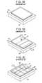
- FIG. 1is a schematic plane view showing a unit liquid crystal panel formed with a thin film transistor array substrate 1 and a color filter substrate 2 attached to face into each other.
- the liquid crystal panel 10includes a picture display unit 13 having a plurality of liquid crystal wells arranged in a matrix form, a gate pad unit 14 connected to a plurality of gate lines of the picture display unit 13 , and a data pad unit 15 connected to the gate pad unit 14 and a plurality of data lines.
- the gate pad unit 14 and the data pad unit 15are formed at the marginal portion of the thin film transistor array substrate 1 .
- the portiondoes not overlap the color filter substrate 2 .
- the gate pad unit 14supplies a scan signal supplied from the gate driver integrated circuit to the gate lines of the picture display unit 13 .
- the data pad unit 15supplies picture information supplied from the data driver integrated circuit to the data lines of the picture display unit 13 .
- the data lines receiving the picture information and the gate lines receiving the scan signalare disposed to be crossed orthogonally on the thin film transistor array substrate 1 of the picture display unit 13 .
- a thin film transistoris formed for switching the liquid crystal cells, and a pixel electrode is formed to be connected to the thin film transistor for driving the liquid crystal cell.
- a protective filmis formed at the entire surface to protect the electrode and the thin film transistor.
- a plurality of color filtersare coated to be separated by cell regions with a black matrix, and a common transparent electrode corresponding to the pixel electrode are formed at the thin film transistor array substrate 1 .
- a cell gapis formed between the thin film transistor array substrate 1 and the color filter substrate 2 so that the two substrates are spaced apart and face into each other.
- the thin film transistor array substrate 1 and the color filter substrate 2are attached by a sealant (not shown) formed at the exterior of the picture display unit 13 .
- a liquid crystal layer(not shown) is formed at the space between the thin film transistor array substrate 1 and the color filter substrate 2 .
- FIG. 2is a cross-sectional view showing a plurality of unit liquid crystal display panels formed in the first mother substrate having the thin film transistor array substrate 1 and the second mother substrate with the color filter substrate 2 .
- a plurality of unit panelsare formed in such a manner that one side of the thin film transistor array substrate 1 is protruded as much as a dummy region 31 .
- the color filter substrate 2 formed on the second mother substrate 30is formed to be isolated as much as dummy regions 31 corresponding to the area that the thin film transistor array substrate 1 formed on the first mother substrate 20 are protruded.
- Each unit panelis disposed at the first and second mother substrates 20 and 30 so that the first and the second mother substrates 20 and 30 are used at the maximum.
- the unit panelsare generally formed to be isolated as much as the dummy region 32 .
- the liquid crystal display panelsare individually cut through the scribing process and the breaking process.
- the dummy regions 31 formed at the region where the color filter substrates 2 of the second mother substrate 30are isolated.
- the dummy region 32 isolating the unit panelsare simultaneously removed.
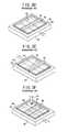
- the first mother substrate 20 and the second mother substrate 30are loaded on a first table 33 .
- the first table 33is moved in one direction to sequentially form a plurality of first scribing lines 42 on the first mother substrate 20 with a cutting wheel 41 .
- first table 33is moved to its original position to sequentially form a plurality of second scribing lines 43 on the surface of the first mother substrate 20 through the cutting wheel 41 .
- FIG. 3Dillustrates the first and second mother substrates 20 and 30 , which are overturned and loaded on a second table 34 . While the second table 34 is moved in one direction, the second mother substrate 30 is pressed by a breaking bar 44 along the second scribing lines 43 so that a crack is transmitted on the first mother substrate 20 .
- the second and first mother substrates 30 and 20are rotated by 90°. While the second table 34 is moved to its original position, the second mother substrate 30 is pressed by the breaking bar 44 along the first scribing lines 42 , so that a crack is transmitted on the first mother substrate 20 .
- the second and first substrates 30 and 20are loaded on a third table 35 .
- a plurality of third scribing lines 46are sequentially formed on the surface of the second mother substrate 30 with a cutting wheel 45 by moving the third table 35 in one direction.
- the second and first mother substrates 30 and 20are rotated by 90°, as shown in FIG. 3G.
- a plurality of fourth scribing lines 47are sequentially formed on the surface of the second mother substrate 30 with the cutting wheel 45 by moving the third table 35 to its original position.
- the second and first mother substrates 30 and 20are overturned and loaded on the fourth table 36 .
- the first mother substrate 20is pressed by a breaking bar 48 along the fourth scribing line 47 by moving the fourth table 36 in one direction, so that a crack is transmitted on the second mother substrate 30 .
- the first and second mother substrates 20 and 30are rotated by 90°, as shown in FIG. 3I.
- the first mother substrate 20is pressed by the breaking bar 48 along the third scribing line 46 by moving the fourth table 36 to its original position, so that a crack is transmitted on the second mother substrate 30 .
- the present inventionis directed to a device for cutting a liquid crystal display panel and a method for cutting using the same that substantially obviates one or more of problems due to limitations and disadvantages of the related art.
- Another object of the present inventionis to provide a device for cutting a liquid crystal display panel and a method for cutting using the same that are capable of reducing the number of scribing and breaking equipments and reducing time required for a process by minimizing rotations and overturnings for performing the scribing and breaking processes.
- a device for cutting a liquid crystal display panelincludes a first scribing unit having first and second wheels for forming a first scribing line on surfaces of first and second mother substrates that are bonded to each other, a first breaking unit for breaking the first and second mother substrates along the first scribing line, and a first rotating unit for rotating the first and second mother substrates to form a second scribing line.
- a device for cutting a liquid crystal display panelincludes a first scribing unit having first and second wheels for forming first scribing lines on surfaces of first and second mother substrates that are bonded to each other, a first breaking unit for breaking the first and second mother substrates along the second scribing line, and a second breaking unit for breaking the cut first and second mother substrates along the first scribing line to separate out into a plurality of liquid crystal display panels.
- a method for cutting a liquid crystal display panelincludes forming a first a first scribing line on surfaces of first and second mother substrates that are bonded to each other, performing a first breaking along the first scribing line, forming a second scribing line on the first and second mother substrates, and performing a second breaking along the second scribing line.
- a method for cutting a liquid crystal display panelincludes forming first and second scribing lines on surfaces of first and second mother substrates that are bonded to each other, performing a first breaking along the second scribing lines, and performing a second breaking the first and second mother substrates.
- FIG. 1is a plane view showing a unit liquid crystal display panel formed in the thin film transistor array substrate and a color filter substrate for a liquid crystal display device, which are attached to face into each other;
- FIG. 2is a cross-sectional view showing a plurality of liquid crystal display panels formed in the first mother substrate including the thin film transistor array substrates and the second mother substrate with the color filter substrate of FIG. 1;
- FIGS. 3A to 3 Jillustrate sequential cutting processes of unit panels in accordance with a related art
- FIG. 4is a schematic block diagram of a device for cutting a liquid crystal display panel in accordance with a first embodiment of the present invention
- FIGS. 5A to 5 Gillustrate sequential processes in each block of FIG. 4;
- FIG. 6is a schematic block diagram of a device for cutting a liquid crystal display panel in accordance with a second embodiment of the present invention.
- FIGS. 7A to 7 Fillustrate sequential processes for performing each block of FIG. 6.
- FIGS. 8A to 8 Cillustrate different alignments of an upper wheel and a lower wheel for simultaneously scribing the first and second mother substrates in accordance with the present invention.
- FIG. 4is a schematic block diagram of a cutter for cutting a liquid crystal display panel in accordance with a first embodiment of the present invention.
- a cutter for cutting a liquid crystal display panel in accordance with the first embodiment of the present inventionincludes a loading unit 60 for loading and aligning first and second mother substrates that are attached to each other, a first scribing unit 61 for forming a plurality of first scribing lines with a first upper wheel and a first lower wheel on the surface of the first and second mother substrates.
- a first breaking unit 62is to break the first and second mother substrates by pressing with first and second breaking bars along the first scribing lines formed on the surface of the first and second mother substrates.
- a first rotating unit 63is to rotate the first and second mother substrates by 90°.
- a second scribing unit 64is to form a plurality of second scribing lines with a second upper wheel and a second lower wheel on the surface of the first and second mother substrates.
- a second breaking unit 65is to break the first and second mother substrates by pressing with a third and a fourth breaking bars along the second scribing lines formed on the surface of the first and second mother substrates and to transmit a crack on the first and second mother substrate.
- an unloading unit 66is to rotate the first and second mother substrate by 90° to be in the direction the same as the initial loading direction, sequentially unloading a plurality of unit liquid crystal panels cut along the first and second scribing lines, and conveying to the equipment for the further processes.
- FIGS. 5A to 5 Gillustrate sequential processes for performing each block of FIG. 4.
- the loading unit 60loads a first mother substrate 110 and a second mother substrate 111 that are attached to each other.
- a plurality of thin film transistor array substratesare formed in the first mother substrate 110
- a plurality of color filter substratesare formed in the second mother substrate 111 .
- the first and second mother substrates 110 and 111are aligned through an alignment mark 130 .
- the first mother substrate 110 including the thin film transistor array substratesis stacked on the second mother substrate 111 including the color filter substrates.
- an impact to a gate pad unit or a data pad unit formed on the thin film transistor array substratemay be minimized by the following breaking process.
- the first scribing unit 61sequentially forms a plurality of first scribing lines 150 and 151 on the surface of the first and second mother substrates 110 and 111 , with a first upper wheel 140 and a first lower wheel 141 , in the space between the first and second tables 120 and 121 .
- the first and second mother substrates 110 and 111move to one direction so that the first and second mother substrates 110 and 111 are placed between the first table 120 and the second table 121 that are isolated by a space therebetween.
- One side of the thin film transistor array substrates formed at the first mother substrate 110is protruded to be longer than the corresponding side of the color filter substrates formed at the second mother substrate 111 . This is because the data pad unit formed at the gate pad unit is formed at one of the left and right sides, and the data pad unit is formed at one of the upper and lower sides of the thin film transistor array substrate.
- the first upper wheel 140is isolated for a certain distance to one side of a reference line R 1 , so as to form a first scribing line 150 on the surface of the first mother substrate 110 .
- the first lower wheel 141is isolated for a certain distance in the opposite direction corresponding to the first upper wheel 140 from the reference line R 1 , so as to form the first scribing line 151 on the surface of the second mother substrate 111 .
- the first upper wheel 140 and the first lower wheel 141are aligned to the straight line, thereby forming the first scribing lines 150 and 151 on the surface of the first and second mother substrates 110 and 111 .
- the first breaking unit 62breaks the first and second mother substrates 110 and 111 by pressing with first and second breaking bars 160 and 161 , along the first scribing lines 150 and 151 formed on the surface of the first and second mother substrates 110 and 111 , in the space between the third and fourth tables 122 and 123 to transmit a crack on the first and second mother substrates 110 and 111 .
- the first and second mother substrates 110 and 111move to be placed between the third and fourth tables 122 and 123 , thereby cutting the first and second mother substrates 110 and 111 .
- the second breaking bar 161supports the second mother substrate 111 .
- the first breaking bar 160supports the first mother substrate 110 .
- FIG. 5Dillustrates the first rotating unit 63 rotating the cut first and second mother substrates 110 and 111 by 90°.
- the second scribing unit 64sequentially forms the second scribing lines 152 and 153 on the surface of the first and second mother substrates 110 and 111 , with the second upper wheel 142 and the second lower wheel 143 located at the space between the fifth and sixth tables 124 and 125 , while the first and second mother substrates 110 and 111 move to be placed between the fifth and sixth tables 124 and 125 that are isolated by the space therebetween.
- one side of the thin film transistor array substrates formed at the first mother substrate 110is protruded to be longer than the corresponding side of the color filter substrates formed at the second mother substrate 111 .
- the second upper wheel 142 and the second lower wheel 143are isolated from each other by a certain distance in the opposite direction along the reference line R 1 , so as to form the second scribing lines 152 and 153 on the surface of the first and second mother substrates 110 and
- the second upper wheel 142 and the second lower wheel 143are aligned to each other, so as to form the second scribing lines 152 and 153 on the surface of the first and second mother substrates 110 and 111 .
- the second breaking unit 65presses the first and second mother substrates 110 and 111 with third and fourth breaking bars 162 and 163 along the second scribing lines 152 and 153 , formed on the surface of the first and second mother substrates 110 and 111 at the space between the seventh and eighth tables 126 and 127 , to transmit a crack on the first and second mother substrates 110 and 111 .
- the first and second mother substrates 110 and 111move to be placed between the seventh and eighth tables 126 and 127 , thereby cutting the first and second mother substrates 110 and 111 .
- the fourth breaking bar 163supports the second mother substrate 111 .
- the third breaking bar 162supports the first mother substrate 110 .
- the unloading unit 66sequentially unloads the unit panels cut along the first and second scribing lines 150 to 153 and conveys to the equipment for the following processes, as shown in FIG. 5G.
- the unit panels conveyed to the unloading unit 66is rotated by 90° compared to the direction of the loading unit 60 , as shown in FIG. 5G.
- a second rotating unit 67is installed in the unloading unit 66 so as to rotate the unit panels by 90° and unloads the unit panels for facilitating the following processes.
- the first overturning unit 68may be installed in the unloading unit 66 to overturn the unloaded unit panels and convey to the equipment in the following processes.
- FIG. 6is a schematic block diagram of a cutter for cutting a liquid crystal display panel in accordance a second embodiment of the present invention.
- the cutter in accordance the second embodiment of the present inventionincludes a loading unit for loading and aligning first and second mother substrates that are attached to face into each other.
- a first scribing unit 210is to sequentially form a plurality of first scribing lines with a first upper wheel and a first lower wheel on the surface of the first and second mother substrates with moving the first and second mother substrates in one direction, rotating the first and second mother substrates by 90°.
- a plurality of second scribing linesare sequentially formed with the first upper wheel and the first lower wheel on the surface of the first and second mother substrates with moving the first and second mother substrates to the original position.
- a first breaking unit 220is to sequentially press the first and second mother substrates with first and second breaking bars along the second scribing lines formed on the surface of the first and second mother substrates with moving the first and second mother substrates in one direction to cut the first and second mother substrates.
- a second breaking unit 230is to rotate the first and second mother substrates by 90°. The first and second mother substrates are sequentially pressed with third and fourth breaking bars along the first scribing lines with moving the first and second mother substrates as much as a predetermined distance in one direction.
- An unloading unit 240is to sequentially unload the unit panels cut along the first and second scribing lines and convey to the equipment for the following processes.
- FIGS. 7A to 7 Fillustrate sequential processes for performing each block of FIG. 6;
- the loading unit 200loads first and second substrates 203 and 204 that thin film transistor array substrates and color filter substrates are formed and attached to face into each other, on a first table 205 .
- the first and second substrates 203 and 204are aligned by an alignment mark 206 , as shown in FIG. 7A.
- the first mother substrate 203 including the thin film transistor array substratesis stacked on the second mother substrate 204 with the color filter substrates.
- an impact to a gate pad unit or a data pad unit formed on the thin film transistor array substratemay be minimized in the following breaking processes.
- the first scribing unit 210sequentially forms the first scribing lines 214 and 215 on the surface of the first and second mother substrates 203 and 204 with the first upper wheel 212 and the first lower wheel 213 in the space between the first and second tables 205 and 211 .
- the first and second mother substrates 203 and 204move to one direction as far as a predetermined distance so that the first and second mother substrates 203 and 204 may be placed between the first table 205 and the second table 211 that are isolated with the space therebetween.
- the first scribing unit 210rotates the first and second mother substrates 203 and 204 having the first scribing lines 214 and 215 by 90°, and sequentially forms a plurality of second scribing lines 216 and 217 on the surface of the first and second mother substrates 203 and 204 with the first upper wheel 212 and the first lower wheel 213 located at the space between the first and second tables 205 and 211 .
- the first and second mother substrates 203 and 204move back to the original position, so as to be placed between the first and second tables 205 and 211 .
- One side of the thin film transistor array substrates formed at the first mother substrate 203is protruded to be longer than the corresponding side of the color filter substrates formed at the second mother substrate 204 .
- the data pad unitis formed at one of the left and right sides and the data pad unit is formed at one of the upper and lower sides of the thin film transistor array substrate.
- the first upper wheel 212is isolated for a certain distance to one side of a reference line R 1 for forming first and second scribing lines 214 and 216 on the surface of the first mother substrate 203 .
- the first lower wheel 213is isolated for a certain distance to the opposite direction corresponding to the first upper wheel 212 from the reference line R 1 for forming the first and second scribing lines 215 and 217 on the surface of the second mother substrate 204 .
- the first upper wheel 212 and the first lower wheel 213are aligned to the straight line.
- the first and second scribing lines 214 to 217are formed on the surface of the first and second mother substrates 203 and 204 .
- the second breaking bar 224supports the second mother substrate 204 .
- the first breaking bar 223supports the first mother substrate 203 .
- the second breaking unit 230rotates the cut first and second mother substrates 203 and 204 by 90°, and presses the first and second mother substrates 203 and 204 with third and fourth breaking bars 233 and 234 along the first scribing lines 214 and 215 formed on the surface of the first and second mother substrates 203 and 204 at the space between the fifth and sixth tables 231 and 232 .
- a crackmoves along the scribing lines in the first and second mother substrates 203 and 204 with moving the first and second mother substrates 203 and 204 to be placed between the fifth and sixth tables 231 and 232 .
- the unit panelsare then cut out from the first and second mother substrates 203 and 204 .
- the fourth breaking bar 234supports the second mother substrate 204 .
- the third breaking bar 233supports the first mother substrate 203 .
- the unloading unit 240sequentially unloads the unit panels cut along the first and second scribing lines 214 to 217 and conveys to the equipment in the following processes.
- the unit panels conveyed to the unloading unit 240is rotated by 90° compared to the direction of the loading unit 200 , as shown in FIG. 7F.
- a second rotating unit 250is installed in the unloading unit 240 so as to rotate the unit panels by 90° and unload the unit panels for more convenient processes.
- the first overturning unit 260may be installed in the unloading unit 240 to overturn the unloaded unit panels and convey to the equipment in the following processes.
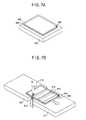
- FIGS. 8A to 8 Cillustrate different alignments of an upper wheel and a lower wheel for simultaneously scribing the first and second mother substrates in accordance with the present invention.
- the scribing wheelmay have to be replaced due to the abrasion.
- the wheelshould be easily replaceable in order to improve productivity.
- FIG. 8Cillustrates another embodiment of the upper wheel 300 and the lower wheel 301 to be symmetrical in the forward-backward direction from the reference line R 1 .
- the scribing and breaking processesare sequentially performed on the first and the second mother substrates with moving the first and second mother substrates.
- sequential scribing and breaking processesmay be performed on the first and second mother substrates with moving the wheel and the breaking bar.
- the device for cutting a liquid crystal display panel and the method for cutting using the same in accordance with the present inventionhave many advantages as follows.
- the liquid crystal display panelsis cut into the unit panels by two simultaneous scribings of the first and second mother substrates, two simultaneous breakings of the first and second mother substrates, and one time of rotation of the first and second mother substrates.
- the liquid crystal display panelis cut to the unit panels by one time of simultaneous scribing of the first and second mother substrates, two simultaneous breakings of the first and second mother substrates, and two rotations of the first and second mother substrates.
- the scribing equipmentis reduced by one as compared to the first embodiment of the present invention, so that the installation expense and installation space of the equipment may be reduced more.
- the upper wheel and the lower wheel for the scribing of the present inventionare positioned to be symmetrical in the horizontal direction and forward-backward direction from the reference line, they may be easily and conveniently replaced. Thus, the time for replacement may be reduced and the productivity may be improved.
Landscapes
- Chemical & Material Sciences (AREA)
- Engineering & Computer Science (AREA)
- Physics & Mathematics (AREA)
- Materials Engineering (AREA)
- Nonlinear Science (AREA)
- Organic Chemistry (AREA)
- Mechanical Engineering (AREA)
- Crystallography & Structural Chemistry (AREA)
- General Physics & Mathematics (AREA)
- Optics & Photonics (AREA)
- Mathematical Physics (AREA)
- Manufacturing & Machinery (AREA)
- Liquid Crystal (AREA)
Abstract
Description
- This application claims the benefit of the Korean Application No. P2002-007179 filed on Feb. 7, 2002, which is hereby incorporated by reference.[0001]
- 1. Field of the Invention[0002]
- The present invention relates to a liquid crystal display panel, and more particularly, to a device for cutting a liquid crystal display panel and a method for cutting using the same to separate a unit liquid crystal display panel from the mother substrate.[0003]
- 2. Discussion of the Related Art[0004]
- In general, a liquid crystal display device displays a desired picture by individually supplying a data signal according to picture information to the liquid crystal cell arranged in a matrix form and controlling light transmittance of the liquid crystal cells.[0005]
- The liquid crystal display device includes a liquid crystal display panel on which liquid crystal cells of a pixel unit are arranged in a matrix form and a driver integrated circuit (IC) for driving the liquid crystal cells.[0006]
- The liquid crystal display panel includes a color filter substrate and a thin film transistor array substrate that are facing into each other and a liquid crystal filled between the color filter substrate and the thin film transistor array substrate.[0007]
- On the thin film transistor array substrate of the liquid crystal panel, there are a plurality of data lines for transmitting a data signal supplied from a data driver integrated circuit to the liquid crystal cell and a plurality of gate lines for transmitting a scan signal supplied from a gate driver integrated circuit to the liquid crystal cells. The liquid crystal cells are defined at each portion where the data lines and the gate lines cross each other.[0008]
- The gate driver integrated circuit sequentially supplies a scan signal to the plurality of gate lines so that the liquid crystal cells arranged in a matrix form are sequentially selected line by line. A data signal is supplied from the data driver integrated circuit to the selected line of the liquid crystal cells.[0009]
- Meanwhile, a common electrode and a pixel electrode are formed on the color filter substrate and the thin film transistor array substrate to face into each other for applying an electric field to the liquid crystal layer.[0010]
- The pixel electrode is formed by liquid crystal cells on the thin film transistor array substrate, while the common electrode is integrally formed on the entire surface of the color filter substrate.[0011]
- Accordingly, by controlling a voltage applied to the pixel electrode while a voltage is applied to the common electrode, the light transmittance of the liquid crystal cells is individually controlled.[0012]
- In order to control the voltage applied to the pixel electrode by each liquid crystal cell, a thin film transistor used as a switching device is formed at each liquid crystal cell.[0013]
- To improve yield in fabricating a liquid crystal display device, a plurality of thin film transistor array substrates are formed on one large mother substrate, and a plurality of color filter substrates are formed on the other mother substrate. The two mother substrates are then attached to simultaneously form the plurality of liquid crystal panels. Thus, a process for cutting the liquid crystal panel into a plurality of unit panels is required.[0014]
- Cutting the liquid crystal display panel is performed by a scribing process for forming a scribing line on the surface of the mother substrate with a pen made of diamond having a hardness higher than that of glass and a breaking process for cutting by applying a mechanical force along the scribing line.[0015]
- The cutting process will now be described in detail with reference to the accompanying drawings.[0016]
- FIG. 1 is a schematic plane view showing a unit liquid crystal panel formed with a thin film transistor array substrate[0017]1 and a
color filter substrate 2 attached to face into each other. - In FIG. 1, the[0018]
liquid crystal panel 10 includes apicture display unit 13 having a plurality of liquid crystal wells arranged in a matrix form, agate pad unit 14 connected to a plurality of gate lines of thepicture display unit 13, and adata pad unit 15 connected to thegate pad unit 14 and a plurality of data lines. - The[0019]
gate pad unit 14 and thedata pad unit 15 are formed at the marginal portion of the thin film transistor array substrate1. The portion does not overlap thecolor filter substrate 2. - The[0020]
gate pad unit 14 supplies a scan signal supplied from the gate driver integrated circuit to the gate lines of thepicture display unit 13. Thedata pad unit 15 supplies picture information supplied from the data driver integrated circuit to the data lines of thepicture display unit 13. - The data lines receiving the picture information and the gate lines receiving the scan signal are disposed to be crossed orthogonally on the thin film transistor array substrate[0021]1 of the
picture display unit 13. At the crossed portion, a thin film transistor is formed for switching the liquid crystal cells, and a pixel electrode is formed to be connected to the thin film transistor for driving the liquid crystal cell. Further, a protective film is formed at the entire surface to protect the electrode and the thin film transistor. - At the[0022]
color filter substrate 2 of thepicture display unit 13, a plurality of color filters are coated to be separated by cell regions with a black matrix, and a common transparent electrode corresponding to the pixel electrode are formed at the thin film transistor array substrate1. - A cell gap is formed between the thin film transistor array substrate[0023]1 and the
color filter substrate 2 so that the two substrates are spaced apart and face into each other. The thin film transistor array substrate1 and thecolor filter substrate 2 are attached by a sealant (not shown) formed at the exterior of thepicture display unit 13. A liquid crystal layer (not shown) is formed at the space between the thin film transistor array substrate1 and thecolor filter substrate 2. - FIG. 2 is a cross-sectional view showing a plurality of unit liquid crystal display panels formed in the first mother substrate having the thin film transistor array substrate[0024]1 and the second mother substrate with the
color filter substrate 2. - As shown in FIG. 2, a plurality of unit panels are formed in such a manner that one side of the thin film transistor array substrate[0025]1 is protruded as much as a
dummy region 31. - This is because the[0026]
gate pad unit 14 and thedata pad unit 15 are formed at the marginal portion where the thin film transistor array substrate1 and thecolor filter substrate 2 do not overlap. - Thus, the[0027]
color filter substrate 2 formed on thesecond mother substrate 30 is formed to be isolated as much asdummy regions 31 corresponding to the area that the thin film transistor array substrate1 formed on thefirst mother substrate 20 are protruded. - Each unit panel is disposed at the first and[0028]
second mother substrates second mother substrates dummy region 32. - After the[0029]
first mother substrate 20 where the thin film transistor array substrates1 are formed and thesecond mother substrate 30 where thecolor filter substrates 2 are formed are attached each other, the liquid crystal display panels are individually cut through the scribing process and the breaking process. Thedummy regions 31 formed at the region where thecolor filter substrates 2 of thesecond mother substrate 30 are isolated. Thedummy region 32 isolating the unit panels are simultaneously removed. - The cutting process to the unit panels will now be described with reference to FIGS. 3A to[0030]3J.
- As shown in FIG. 3A, the[0031]
first mother substrate 20 and thesecond mother substrate 30 are loaded on a first table33. - Next, as shown in FIG. 3B, the first table[0032]33 is moved in one direction to sequentially form a plurality of first
scribing lines 42 on thefirst mother substrate 20 with acutting wheel 41. - After first and[0033]
second mother substrates scribing lines 43 on the surface of thefirst mother substrate 20 through thecutting wheel 41. - FIG. 3D illustrates the first and[0034]
second mother substrates second mother substrate 30 is pressed by abreaking bar 44 along the secondscribing lines 43 so that a crack is transmitted on thefirst mother substrate 20. - Next, as shown in FIG. 3E, the second and[0035]
first mother substrates second mother substrate 30 is pressed by thebreaking bar 44 along the firstscribing lines 42, so that a crack is transmitted on thefirst mother substrate 20. - As shown in FIG. 3F, the second and[0036]
first substrates scribing lines 46 are sequentially formed on the surface of thesecond mother substrate 30 with acutting wheel 45 by moving the third table35 in one direction. - Thereafter, the second and[0037]
first mother substrates fourth scribing lines 47 are sequentially formed on the surface of thesecond mother substrate 30 with thecutting wheel 45 by moving the third table35 to its original position. - As shown in FIG. 3H, the second and first mother substrates[0038]30 and20 are overturned and loaded on the fourth table36. The
first mother substrate 20 is pressed by a breakingbar 48 along thefourth scribing line 47 by moving the fourth table36 in one direction, so that a crack is transmitted on thesecond mother substrate 30. - Next, the first and second mother substrates[0039]20 and30 are rotated by 90°, as shown in FIG. 3I. The
first mother substrate 20 is pressed by the breakingbar 48 along thethird scribing line 46 by moving the fourth table36 to its original position, so that a crack is transmitted on thesecond mother substrate 30. - As shown in FIG. 3J, as the crack is transmitted on first and second mother substrates[0040]20 and30 along first through
fourth scribing lines vacuum gripper 49 and conveyed to the equipment for next processes. - As mentioned above, in the conventional cutting device and cutting processes for the unit panel, scribing is performed four times and breaking is performed four times through four rotation processes and two overturning processes.[0041]
- Thus, two scribing units including a rotating unit and two breaking units including a rotating unit and an overturning unit are required. These equipments would occupy much space in the working place. Thus, an installation expense and a space of the equipment are wasted.[0042]
- In addition, much time is required for the scribing and breaking processes, resulting in a low productivity.[0043]
- Accordingly, the present invention is directed to a device for cutting a liquid crystal display panel and a method for cutting using the same that substantially obviates one or more of problems due to limitations and disadvantages of the related art.[0044]
- Another object of the present invention is to provide a device for cutting a liquid crystal display panel and a method for cutting using the same that are capable of reducing the number of scribing and breaking equipments and reducing time required for a process by minimizing rotations and overturnings for performing the scribing and breaking processes.[0045]
- Additional features and advantages of the invention will be set forth in the description which follows and in part will be apparent from the description, or may be learned by practice of the invention. The objectives and other advantages of the invention will be realized and attained by the structure particularly pointed out in the written description and claims hereof as well as the appended drawings.[0046]
- To achieve these and other advantages and in accordance with the purpose of the present invention, as embodied and broadly described, a device for cutting a liquid crystal display panel includes a first scribing unit having first and second wheels for forming a first scribing line on surfaces of first and second mother substrates that are bonded to each other, a first breaking unit for breaking the first and second mother substrates along the first scribing line, and a first rotating unit for rotating the first and second mother substrates to form a second scribing line.[0047]
- In another aspect of the present invention, a device for cutting a liquid crystal display panel includes a first scribing unit having first and second wheels for forming first scribing lines on surfaces of first and second mother substrates that are bonded to each other, a first breaking unit for breaking the first and second mother substrates along the second scribing line, and a second breaking unit for breaking the cut first and second mother substrates along the first scribing line to separate out into a plurality of liquid crystal display panels.[0048]
- In another aspect of the present invention, a method for cutting a liquid crystal display panel includes forming a first a first scribing line on surfaces of first and second mother substrates that are bonded to each other, performing a first breaking along the first scribing line, forming a second scribing line on the first and second mother substrates, and performing a second breaking along the second scribing line.[0049]
- In a further aspect of the present invention, a method for cutting a liquid crystal display panel includes forming first and second scribing lines on surfaces of first and second mother substrates that are bonded to each other, performing a first breaking along the second scribing lines, and performing a second breaking the first and second mother substrates.[0050]
- It is to be understood that both the foregoing general description and the following detailed description are exemplary and explanatory and are intended to provide further explanation of the invention as claimed.[0051]
- The accompanying drawings, which are included to provide a further understanding of the invention and are incorporated in and constitute a part of this application, illustrate embodiments of the invention and together with the description serve to explain the principle of the invention.[0052]
- In the drawings:[0053]
- FIG. 1 is a plane view showing a unit liquid crystal display panel formed in the thin film transistor array substrate and a color filter substrate for a liquid crystal display device, which are attached to face into each other;[0054]
- FIG. 2 is a cross-sectional view showing a plurality of liquid crystal display panels formed in the first mother substrate including the thin film transistor array substrates and the second mother substrate with the color filter substrate of FIG. 1;[0055]
- FIGS. 3A to[0056]3J illustrate sequential cutting processes of unit panels in accordance with a related art;
- FIG. 4 is a schematic block diagram of a device for cutting a liquid crystal display panel in accordance with a first embodiment of the present invention;[0057]
- FIGS. 5A to[0058]5G illustrate sequential processes in each block of FIG. 4;
- FIG. 6 is a schematic block diagram of a device for cutting a liquid crystal display panel in accordance with a second embodiment of the present invention;[0059]
- FIGS. 7A to[0060]7F illustrate sequential processes for performing each block of FIG. 6; and
- FIGS. 8A to[0061]8C illustrate different alignments of an upper wheel and a lower wheel for simultaneously scribing the first and second mother substrates in accordance with the present invention.
- Reference will now be made in detail to the illustrated embodiments of the present invention, examples of which are illustrated in the accompanying drawings. Wherever possible, the same reference numbers will be used throughout the drawings to refer to the same or like parts.[0062]
- FIG. 4 is a schematic block diagram of a cutter for cutting a liquid crystal display panel in accordance with a first embodiment of the present invention.[0063]
- As shown in FIG. 4, a cutter for cutting a liquid crystal display panel in accordance with the first embodiment of the present invention includes a[0064]
loading unit 60 for loading and aligning first and second mother substrates that are attached to each other, afirst scribing unit 61 for forming a plurality of first scribing lines with a first upper wheel and a first lower wheel on the surface of the first and second mother substrates. Afirst breaking unit 62 is to break the first and second mother substrates by pressing with first and second breaking bars along the first scribing lines formed on the surface of the first and second mother substrates. A firstrotating unit 63 is to rotate the first and second mother substrates by 90°. Asecond scribing unit 64 is to form a plurality of second scribing lines with a second upper wheel and a second lower wheel on the surface of the first and second mother substrates. Asecond breaking unit 65 is to break the first and second mother substrates by pressing with a third and a fourth breaking bars along the second scribing lines formed on the surface of the first and second mother substrates and to transmit a crack on the first and second mother substrate. Further, anunloading unit 66 is to rotate the first and second mother substrate by 90° to be in the direction the same as the initial loading direction, sequentially unloading a plurality of unit liquid crystal panels cut along the first and second scribing lines, and conveying to the equipment for the further processes. - FIGS. 5A to[0065]5G illustrate sequential processes for performing each block of FIG. 4.
- As shown in FIG. 5A, the[0066]
loading unit 60 loads afirst mother substrate 110 and asecond mother substrate 111 that are attached to each other. A plurality of thin film transistor array substrates are formed in thefirst mother substrate 110, and a plurality of color filter substrates are formed in thesecond mother substrate 111. The first andsecond mother substrates alignment mark 130. - The[0067]
first mother substrate 110 including the thin film transistor array substrates is stacked on thesecond mother substrate 111 including the color filter substrates. When the first andsecond mother substrates - In FIG. 5B, the[0068]
first scribing unit 61 sequentially forms a plurality offirst scribing lines second mother substrates upper wheel 140 and a first lower wheel141, in the space between the first and second tables120 and121. The first andsecond mother substrates second mother substrates - One side of the thin film transistor array substrates formed at the[0069]
first mother substrate 110 is protruded to be longer than the corresponding side of the color filter substrates formed at thesecond mother substrate 111. This is because the data pad unit formed at the gate pad unit is formed at one of the left and right sides, and the data pad unit is formed at one of the upper and lower sides of the thin film transistor array substrate. - Accordingly, at the region where one side of the thin film transistor array substrates is protruded to be longer than the corresponding side of the color filter substrates, the first[0070]
upper wheel 140 is isolated for a certain distance to one side of a reference line R1, so as to form afirst scribing line 150 on the surface of thefirst mother substrate 110. The first lower wheel141 is isolated for a certain distance in the opposite direction corresponding to the firstupper wheel 140 from the reference line R1, so as to form thefirst scribing line 151 on the surface of thesecond mother substrate 111. - At the region where no gate pad unit or data pad unit of the thin film transistor array substrates is formed (that is, the region where the thin film transistor array substrates are not protruded to be longer than the color filter substrates), the first[0071]
upper wheel 140 and the first lower wheel141 are aligned to the straight line, thereby forming thefirst scribing lines second mother substrates - As shown in FIG. 5C, the[0072]
first breaking unit 62 breaks the first andsecond mother substrates first scribing lines second mother substrates second mother substrates second mother substrates second mother substrates - When the[0073]
first mother substrate 110 is pressed by thefirst breaking bar 160, thesecond breaking bar 161 supports thesecond mother substrate 111. When thesecond mother substrate 111 is pressed by thesecond breaking bar 161, thefirst breaking bar 160 supports thefirst mother substrate 110. - FIG. 5D illustrates the first[0074]
rotating unit 63 rotating the cut first andsecond mother substrates - As shown in FIG. 5E, the[0075]
second scribing unit 64 sequentially forms thesecond scribing lines second mother substrates upper wheel 142 and the secondlower wheel 143 located at the space between the fifth and sixth tables124 and125, while the first andsecond mother substrates - As mentioned above, one side of the thin film transistor array substrates formed at the[0076]
first mother substrate 110 is protruded to be longer than the corresponding side of the color filter substrates formed at thesecond mother substrate 111. Thus, at the protruded region, like the firstupper wheel 140 and the first lower wheel141, the secondupper wheel 142 and the secondlower wheel 143 are isolated from each other by a certain distance in the opposite direction along the reference line R1, so as to form thesecond scribing lines second mother substrates 110 and - Meanwhile, at the region where the thin film transistor array substrates are not protruded to be longer than the color filter substrates, like the first[0077]
upper wheel 140 and the first lower wheel141, the secondupper wheel 142 and the secondlower wheel 143 are aligned to each other, so as to form thesecond scribing lines second mother substrates - In FIG. 5F, the[0078]
second breaking unit 65 presses the first andsecond mother substrates second scribing lines second mother substrates second mother substrates second mother substrates second mother substrates - When the[0079]
first mother substrate 110 is pressed by thethird breaking bar 162, thefourth breaking bar 163 supports thesecond mother substrate 111. When thesecond mother substrate 111 is pressed by thefourth breaking bar 163, thethird breaking bar 162 supports thefirst mother substrate 110. - The[0080]
unloading unit 66 sequentially unloads the unit panels cut along the first andsecond scribing lines 150 to153 and conveys to the equipment for the following processes, as shown in FIG. 5G. - Meanwhile, the unit panels conveyed to the[0081]
unloading unit 66 is rotated by 90° compared to the direction of theloading unit 60, as shown in FIG. 5G. A secondrotating unit 67 is installed in theunloading unit 66 so as to rotate the unit panels by 90° and unloads the unit panels for facilitating the following processes. - In addition, in the following process, when a unit panel requires a state that the color filter substrate is stacked on the thin film transistor array substrate, as shown in FIG. 5G, the[0082]
first overturning unit 68 may be installed in theunloading unit 66 to overturn the unloaded unit panels and convey to the equipment in the following processes. - As aforementioned, referring to the cutter for cutting a liquid crystal display panel and the method for cutting using the same in accordance with the first embodiment of the present invention, there requires only two simultaneous scribings of the first and second mother substrates and two simultaneous breakings of the first and second mother substrates. Also, the formed liquid crystal display panels are individually cut into the unit panels by rotating the first and second mother substrates once only.[0083]
- FIG. 6 is a schematic block diagram of a cutter for cutting a liquid crystal display panel in accordance a second embodiment of the present invention.[0084]
- As shown in FIG. 6, the cutter in accordance the second embodiment of the present invention includes a loading unit for loading and aligning first and second mother substrates that are attached to face into each other. A[0085]
first scribing unit 210 is to sequentially form a plurality of first scribing lines with a first upper wheel and a first lower wheel on the surface of the first and second mother substrates with moving the first and second mother substrates in one direction, rotating the first and second mother substrates by 90°. A plurality of second scribing lines are sequentially formed with the first upper wheel and the first lower wheel on the surface of the first and second mother substrates with moving the first and second mother substrates to the original position. Afirst breaking unit 220 is to sequentially press the first and second mother substrates with first and second breaking bars along the second scribing lines formed on the surface of the first and second mother substrates with moving the first and second mother substrates in one direction to cut the first and second mother substrates. Asecond breaking unit 230 is to rotate the first and second mother substrates by 90°. The first and second mother substrates are sequentially pressed with third and fourth breaking bars along the first scribing lines with moving the first and second mother substrates as much as a predetermined distance in one direction. Anunloading unit 240 is to sequentially unload the unit panels cut along the first and second scribing lines and convey to the equipment for the following processes. - FIGS. 7A to[0086]7F illustrate sequential processes for performing each block of FIG. 6;
- Initially, the[0087]
loading unit 200 loads first andsecond substrates second substrates alignment mark 206, as shown in FIG. 7A. - The[0088]
first mother substrate 203 including the thin film transistor array substrates is stacked on thesecond mother substrate 204 with the color filter substrates. When the first andsecond mother substrates - In FIG. 7B, the[0089]
first scribing unit 210 sequentially forms thefirst scribing lines second mother substrates upper wheel 212 and the firstlower wheel 213 in the space between the first and second tables205 and211. In this process, the first andsecond mother substrates second mother substrates - As shown in FIG. 7C, the[0090]
first scribing unit 210 rotates the first andsecond mother substrates first scribing lines second scribing lines second mother substrates upper wheel 212 and the firstlower wheel 213 located at the space between the first and second tables205 and211. In this process, the first andsecond mother substrates - One side of the thin film transistor array substrates formed at the[0091]
first mother substrate 203 is protruded to be longer than the corresponding side of the color filter substrates formed at thesecond mother substrate 204. - This is because the data pad unit is formed at one of the left and right sides and the data pad unit is formed at one of the upper and lower sides of the thin film transistor array substrate.[0092]
- Accordingly, at the region where one side of the thin film transistor array substrates is protruded to be longer than the corresponding side of the color filter substrates, the first[0093]
upper wheel 212 is isolated for a certain distance to one side of a reference line R1 for forming first andsecond scribing lines first mother substrate 203. The firstlower wheel 213 is isolated for a certain distance to the opposite direction corresponding to the firstupper wheel 212 from the reference line R1 for forming the first andsecond scribing lines second mother substrate 204. - Meanwhile, at the region where no gate pad unit or data pad unit of the thin film transistor array substrates is formed (that is, the region where the thin film transistor array substrates are not protruded to be longer than the color filter substrates), the first[0094]
upper wheel 212 and the firstlower wheel 213 are aligned to the straight line. Thus, the first andsecond scribing lines 214 to217 are formed on the surface of the first andsecond mother substrates first breaking unit 220 in FIG. 7D presses the first andsecond mother substrates second scribing lines second mother substrates second mother substrates second mother substrates second mother substrates - When the[0095]
first mother substrate 203 is pressed by thefirst breaking bar 223, thesecond breaking bar 224 supports thesecond mother substrate 204. When thesecond mother substrate 204 is pressed by thesecond breaking bar 224, thefirst breaking bar 223 supports thefirst mother substrate 203. - As shown in FIG. 7E, the[0096]
second breaking unit 230 rotates the cut first andsecond mother substrates second mother substrates first scribing lines second mother substrates second mother substrates second mother substrates second mother substrates - When the[0097]
third breaking bar 233 presses thefirst mother substrate 203, thefourth breaking bar 234 supports thesecond mother substrate 204. When thefourth breaking bar 234 presses thesecond mother substrate 204, thethird breaking bar 233 supports thefirst mother substrate 203. - As shown in FIG. 7F, the[0098]
unloading unit 240 sequentially unloads the unit panels cut along the first andsecond scribing lines 214 to217 and conveys to the equipment in the following processes. - Meanwhile, the unit panels conveyed to the[0099]
unloading unit 240 is rotated by 90° compared to the direction of theloading unit 200, as shown in FIG. 7F. A secondrotating unit 250 is installed in theunloading unit 240 so as to rotate the unit panels by 90° and unload the unit panels for more convenient processes. - In addition, in the following process, when a unit panel requires a state that the color filter substrate is stacked on the thin film transistor array substrate, as shown in FIG. 7F, the[0100]
first overturning unit 260 may be installed in theunloading unit 240 to overturn the unloaded unit panels and convey to the equipment in the following processes. - As aforementioned, referring to the device for cutting a liquid crystal display panel and the method for cutting using the same in accordance with the second embodiment of the present invention, there requires only one time of simultaneous scribing of the first and second mother substrates and two simultaneous breakings of the first and second mother substrates. Also, the liquid crystal display panel is cut into the unit panels by rotating the first and second mother substrates twice.[0101]
- FIGS. 8A to[0102]8C illustrate different alignments of an upper wheel and a lower wheel for simultaneously scribing the first and second mother substrates in accordance with the present invention.
- The scribing wheel may have to be replaced due to the abrasion. Thus, the wheel should be easily replaceable in order to improve productivity.[0103]
- As shown in FIG. 8A, when an[0104]
upper wheel 300 and alower wheel 301 are aligned to the reference line R1, they are not easily replaceable and much time is required for a replacement. - Conversely, when the[0105]
upper wheel 300 and thelower wheel 301 are positioned to be symmetrical in the horizontal direction from the reference line R1, as shown in FIG. 8B, their replacement would be convenient and quick. - FIG. 8C illustrates another embodiment of the[0106]
upper wheel 300 and thelower wheel 301 to be symmetrical in the forward-backward direction from the reference line R1. - In both of the embodiments of the present invention as described above, the scribing and breaking processes are sequentially performed on the first and the second mother substrates with moving the first and second mother substrates. Alternatively, sequential scribing and breaking processes may be performed on the first and second mother substrates with moving the wheel and the breaking bar.[0107]
- As described above, the device for cutting a liquid crystal display panel and the method for cutting using the same in accordance with the present invention have many advantages as follows.[0108]
- That is, referring to the first embodiment, the liquid crystal display panels is cut into the unit panels by two simultaneous scribings of the first and second mother substrates, two simultaneous breakings of the first and second mother substrates, and one time of rotation of the first and second mother substrates.[0109]
- Therefore, the time required for the scribing is minimized compared to that of the conventional art. Also, since the overturning unit is not necessary to overturn the first and second mother substrates, the time required for the scribing and overturning is reduced and productivity is improved. In addition, the problem of wasting an installation expense and an installation space of the equipment is prevented.[0110]
- With respect to the second embodiment, the liquid crystal display panel is cut to the unit panels by one time of simultaneous scribing of the first and second mother substrates, two simultaneous breakings of the first and second mother substrates, and two rotations of the first and second mother substrates.[0111]
- Therefore, the scribing equipment is reduced by one as compared to the first embodiment of the present invention, so that the installation expense and installation space of the equipment may be reduced more.[0112]
- In addition, since the upper wheel and the lower wheel for the scribing of the present invention are positioned to be symmetrical in the horizontal direction and forward-backward direction from the reference line, they may be easily and conveniently replaced. Thus, the time for replacement may be reduced and the productivity may be improved.[0113]
- It will be apparent to those skilled in the art that various modifications and variations can be made in the cutter for cutting a liquid crystal panel and the method for cutting using the same of the present invention without departing from the spirit or scope of the inventions. Thus, it is intended that the present invention covers the modifications and variations of this invention provided they come within the scope of the appended claims and their equivalents.[0114]
Claims (19)
Applications Claiming Priority (3)
| Application Number | Priority Date | Filing Date | Title |
|---|---|---|---|
| KRP2002-007179 | 2002-02-07 | ||
| KR1020020007179AKR100817129B1 (en) | 2002-02-07 | 2002-02-07 | Cutting device and method of liquid crystal panel |
| KR2002-7179 | 2002-02-07 |
Related Child Applications (1)
| Application Number | Title | Priority Date | Filing Date |
|---|---|---|---|
| US10/804,492DivisionUS7052985B2 (en) | 2001-04-19 | 2004-03-18 | Contact structure for an integrated semiconductor device |
Publications (2)
| Publication Number | Publication Date |
|---|---|
| US20030147035A1true US20030147035A1 (en) | 2003-08-07 |
| US6747725B2 US6747725B2 (en) | 2004-06-08 |
Family
ID=27656412
Family Applications (1)
| Application Number | Title | Priority Date | Filing Date |
|---|---|---|---|
| US10/126,939Expired - LifetimeUS6747725B2 (en) | 2002-02-07 | 2002-04-22 | Device for cutting liquid crystal display panel and method for cutting using the same |
Country Status (4)
| Country | Link |
|---|---|
| US (1) | US6747725B2 (en) |
| JP (1) | JP3845054B2 (en) |
| KR (1) | KR100817129B1 (en) |
| CN (1) | CN1229207C (en) |
Cited By (10)
| Publication number | Priority date | Publication date | Assignee | Title |
|---|---|---|---|---|
| US20030155392A1 (en)* | 2002-02-19 | 2003-08-21 | Lg.Philips Lcd Co., Ltd. | Apparatus for cutting liquid crystal display panels and cutting method using the same |
| US20060097022A1 (en)* | 2004-11-05 | 2006-05-11 | Lg. Philips Lcd Co., Ltd. | Scribing apparatus, substrate cutting apparatus equipped with the scribing apparatus, and substrate cutting method using the substrate cutting apparatus |
| US20060285064A1 (en)* | 2005-06-20 | 2006-12-21 | Lee Jeong J | Liquid crystal display panel cutting system and method and liquid crystal display device fabricating method using the same |
| CN103412432A (en)* | 2013-08-29 | 2013-11-27 | 深圳市华星光电技术有限公司 | Liquid crystal panel piece cracking device and piece cracking method |
| KR20160046282A (en)* | 2014-10-20 | 2016-04-28 | 미쓰보시 다이야몬도 고교 가부시키가이샤 | Scribing method and scribing apparatus |
| US20160229732A1 (en)* | 2014-05-16 | 2016-08-11 | Shenzhen China Star Optoelectronics Technology Co. Ltd. | Method for cutting single sheet of glass substrate |
| US20160280579A1 (en)* | 2013-12-27 | 2016-09-29 | Asahi Glass Company, Limited | Method for processing brittle plate, and device for processing brittle plate |
| US20170008794A1 (en)* | 2014-03-27 | 2017-01-12 | Shenzhen China Star Optoelectronics Technology | Glass Substrate Cutting Apparatus and Cutting Method Thereof |
| TWI573768B (en)* | 2011-11-16 | 2017-03-11 | Nippon Electric Glass Co | Plate glass cutting device, plate glass cutting method, plate glass production method and plate glass cutting system |
| IT201600079945A1 (en)* | 2016-07-29 | 2018-01-29 | 2M S R L | APPARATUS FOR WORKING GLASS SHEETS. |
Families Citing this family (21)
| Publication number | Priority date | Publication date | Assignee | Title |
|---|---|---|---|---|
| KR100724474B1 (en)* | 2002-10-22 | 2007-06-04 | 엘지.필립스 엘시디 주식회사 | Device for cutting liquid crystal display panel and method for cutting the same |
| KR101003610B1 (en) | 2003-09-24 | 2010-12-23 | 엘지디스플레이 주식회사 | Cutting device for liquid crystal display panel and cutting method |
| KR100689314B1 (en)* | 2003-11-29 | 2007-03-08 | 엘지.필립스 엘시디 주식회사 | Cutting Method of LCD Panel |
| CN1861339B (en)* | 2005-05-12 | 2013-02-27 | 统宝光电股份有限公司 | Carrier tray for cutting panel and method for manufacturing panel using the same |
| JP2007156310A (en)* | 2005-12-08 | 2007-06-21 | Nec Lcd Technologies Ltd | Manufacturing method of liquid crystal panel |
| KR100788199B1 (en)* | 2006-07-18 | 2007-12-26 | 주식회사 에스에프에이 | Substrate Cutting System and Method |
| JP4240111B2 (en)* | 2006-11-06 | 2009-03-18 | セイコーエプソン株式会社 | Manufacturing method of electro-optical device |
| KR100905898B1 (en)* | 2007-11-21 | 2009-07-02 | 세메스 주식회사 | Scribing device and substrate cutting device and method using same |
| KR101010310B1 (en)* | 2008-05-06 | 2011-01-25 | 세메스 주식회사 | Scribing device and substrate cutting device and method using same |
| JP5156085B2 (en)* | 2010-12-13 | 2013-03-06 | 三星ダイヤモンド工業株式会社 | Method for dividing bonded substrates |
| WO2013089125A1 (en)* | 2011-12-12 | 2013-06-20 | 日本電気硝子株式会社 | Method for cutting and separating plate glass and device for cutting and separating plate glass |
| JP5981791B2 (en)* | 2012-07-18 | 2016-08-31 | 三星ダイヤモンド工業株式会社 | Breaking device for brittle material substrate |
| JP6140012B2 (en)* | 2013-07-08 | 2017-05-31 | 三星ダイヤモンド工業株式会社 | Breaking method for bonded substrates |
| US20160151929A1 (en)* | 2013-07-08 | 2016-06-02 | Kawasaki Jukogyo Kabushiki Kaisha | Method of and apparatus for dividing plate member made of brittle material |
| JP6207307B2 (en)* | 2013-09-03 | 2017-10-04 | 三星ダイヤモンド工業株式会社 | Break device |
| CN105093614A (en)* | 2015-07-30 | 2015-11-25 | 武汉华星光电技术有限公司 | Panel cutting method and device |
| TWI614198B (en)* | 2015-10-21 | 2018-02-11 | Splitting process equipment and method thereof | |
| CN105382946A (en)* | 2015-12-17 | 2016-03-09 | 哈尔滨新力光电技术有限公司 | Automatic efficient splintering machine and method for sapphire LED bar |
| CN105785615A (en)* | 2016-05-23 | 2016-07-20 | 武汉华星光电技术有限公司 | Substrate cutting method and substrate cutting device |
| CN111499173B (en)* | 2020-04-29 | 2020-12-01 | 深圳市弗塔信息技术有限公司 | Method and device for changing size of liquid crystal display |
| KR102678160B1 (en) | 2023-06-09 | 2024-06-25 | 주식회사 신돈축산유통 | dicer device for improving meat cutting speed performance |
Citations (32)
| Publication number | Priority date | Publication date | Assignee | Title |
|---|---|---|---|---|
| US3978580A (en)* | 1973-06-28 | 1976-09-07 | Hughes Aircraft Company | Method of fabricating a liquid crystal display |
| US4653864A (en)* | 1986-02-26 | 1987-03-31 | Ovonic Imaging Systems, Inc. | Liquid crystal matrix display having improved spacers and method of making same |
| US4775225A (en)* | 1985-05-16 | 1988-10-04 | Canon Kabushiki Kaisha | Liquid crystal device having pillar spacers with small base periphery width in direction perpendicular to orientation treatment |
| US5247377A (en)* | 1988-07-23 | 1993-09-21 | Rohm Gmbh Chemische Fabrik | Process for producing anisotropic liquid crystal layers on a substrate |
| US5263888A (en)* | 1992-02-20 | 1993-11-23 | Matsushita Electric Industrial Co., Ltd. | Method of manufacture of liquid crystal display panel |
| US5379139A (en)* | 1986-08-20 | 1995-01-03 | Semiconductor Energy Laboratory Co., Ltd. | Liquid crystal device and method for manufacturing same with spacers formed by photolithography |
| US5406989A (en)* | 1993-10-12 | 1995-04-18 | Ayumi Industry Co., Ltd. | Method and dispenser for filling liquid crystal into LCD cell |
| US5499128A (en)* | 1993-03-15 | 1996-03-12 | Kabushiki Kaisha Toshiba | Liquid crystal display device with acrylic polymer spacers and method of manufacturing the same |
| US5507323A (en)* | 1993-10-12 | 1996-04-16 | Fujitsu Limited | Method and dispenser for filling liquid crystal into LCD cell |
| US5539545A (en)* | 1993-05-18 | 1996-07-23 | Semiconductor Energy Laboratory Co., Ltd. | Method of making LCD in which resin columns are cured and the liquid crystal is reoriented |
| US5548429A (en)* | 1993-06-14 | 1996-08-20 | Canon Kabushiki Kaisha | Process for producing liquid crystal device whereby curing the sealant takes place after pre-baking the substrates |
| US5642214A (en)* | 1991-07-19 | 1997-06-24 | Sharp Kabushiki Kaisha | Optical modulating element and electronic apparatus using it |
| US5742370A (en)* | 1996-09-12 | 1998-04-21 | Korea Institute Of Science And Technology | Fabrication method for liquid crystal alignment layer by magnetic field treatment |
| US5757451A (en)* | 1995-09-08 | 1998-05-26 | Kabushiki Kaisha Toshiba | Liquid crystal display device spacers formed from stacked color layers |
| US5852484A (en)* | 1994-09-26 | 1998-12-22 | Matsushita Electric Industrial Co., Ltd. | Liquid crystal display panel and method and device for manufacturing the same |
| US5861932A (en)* | 1997-03-31 | 1999-01-19 | Denso Corporation | Liquid crystal cell and its manufacturing method |
| US5952676A (en)* | 1986-08-20 | 1999-09-14 | Semiconductor Energy Laboratory Co., Ltd. | Liquid crystal device and method for manufacturing same with spacers formed by photolithography |
| US5956112A (en)* | 1995-10-02 | 1999-09-21 | Sharp Kabushiki Kaisha | Liquid crystal display device and method for manufacturing the same |
| US6001203A (en)* | 1995-03-01 | 1999-12-14 | Matsushita Electric Industrial Co., Ltd. | Production process of liquid crystal display panel, seal material for liquid crystal cell and liquid crystal display |
| US6011609A (en)* | 1996-10-05 | 2000-01-04 | Samsung Electronics Co., Ltd. | Method of manufacturing LCD by dropping liquid crystals on a substrate and then pressing the substrates |
| US6016178A (en)* | 1996-09-13 | 2000-01-18 | Sony Corporation | Reflective guest-host liquid-crystal display device |
| US6016181A (en)* | 1996-11-07 | 2000-01-18 | Sharp Kabushiki Kaisha | Liquid crystal device having column spacers with portion on each of the spacers for reflecting or absorbing visible light and method for fabricating the same |
| US6055035A (en)* | 1998-05-11 | 2000-04-25 | International Business Machines Corporation | Method and apparatus for filling liquid crystal display (LCD) panels |
| US6163357A (en)* | 1996-09-26 | 2000-12-19 | Kabushiki Kaisha Toshiba | Liquid crystal display device having the driving circuit disposed in the seal area, with different spacer density in driving circuit area than display area |
| US6195149B1 (en)* | 1995-11-02 | 2001-02-27 | Seiko Epson Corporation | Method for producing a liquid crystal panel |
| US6219126B1 (en)* | 1998-11-20 | 2001-04-17 | International Business Machines Corporation | Panel assembly for liquid crystal displays having a barrier fillet and an adhesive fillet in the periphery |
| US6226067B1 (en)* | 1997-10-03 | 2001-05-01 | Minolta Co., Ltd. | Liquid crystal device having spacers and manufacturing method thereof |
| US6236445B1 (en)* | 1996-02-22 | 2001-05-22 | Hughes Electronics Corporation | Method for making topographic projections |
| US6304306B1 (en)* | 1995-02-17 | 2001-10-16 | Sharp Kabushiki Kaisha | Liquid crystal display device and method for producing the same |
| US6337730B1 (en)* | 1998-06-02 | 2002-01-08 | Denso Corporation | Non-uniformly-rigid barrier wall spacers used to correct problems caused by thermal contraction of smectic liquid crystal material |
| US6414733B1 (en)* | 1999-02-08 | 2002-07-02 | Dai Nippon Printing Co., Ltd. | Color liquid crystal display with a shielding member being arranged between sealing member and display zone |
| US6470782B1 (en)* | 1997-09-25 | 2002-10-29 | Beldex Corporation | Scribe device |
Family Cites Families (114)
| Publication number | Priority date | Publication date | Assignee | Title |
|---|---|---|---|---|
| JPS5165656A (en) | 1974-12-04 | 1976-06-07 | Shinshu Seiki Kk | |
| JPS52149725A (en) | 1976-06-07 | 1977-12-13 | Ichikoh Ind Ltd | Non contact system lamp checker for vehicle |
| US4094058A (en) | 1976-07-23 | 1978-06-13 | Omron Tateisi Electronics Co. | Method of manufacture of liquid crystal displays |
| JPS5738414A (en) | 1980-08-20 | 1982-03-03 | Showa Denko Kk | Spacer for display panel |
| JPS5788428A (en) | 1980-11-20 | 1982-06-02 | Ricoh Elemex Corp | Manufacture of liquid crystal display body device |
| JPS5827126A (en) | 1981-08-11 | 1983-02-17 | Nec Corp | Production of liquid crystal display panel |
| JPS5957221A (en) | 1982-09-28 | 1984-04-02 | Asahi Glass Co Ltd | Production of display element |
| JPS59195222A (en) | 1983-04-19 | 1984-11-06 | Matsushita Electric Ind Co Ltd | Manufacture of liquid-crystal panel |
| JPS60111221A (en) | 1983-11-19 | 1985-06-17 | Nippon Denso Co Ltd | Method and device for charging liquid crystal |
| JPS60164723A (en) | 1984-02-07 | 1985-08-27 | Seiko Instr & Electronics Ltd | Liquid crystal display device |
| JPS60217343A (en) | 1984-04-13 | 1985-10-30 | Matsushita Electric Ind Co Ltd | Liquid crystal display device and its preparation |
| JPS617822A (en) | 1984-06-22 | 1986-01-14 | Canon Inc | Production of liquid crystal element |
| JPS6155625A (en) | 1984-08-24 | 1986-03-20 | Nippon Denso Co Ltd | Manufacture of liquid crystal element |
| US4691995A (en) | 1985-07-15 | 1987-09-08 | Semiconductor Energy Laboratory Co., Ltd. | Liquid crystal filling device |
| JPS6289025A (en) | 1985-10-15 | 1987-04-23 | Matsushita Electric Ind Co Ltd | Manufacturing method of liquid crystal display panel |
| JPS6290622A (en) | 1985-10-17 | 1987-04-25 | Seiko Epson Corp | liquid crystal display device |
| JPH0668589B2 (en) | 1986-03-06 | 1994-08-31 | キヤノン株式会社 | Ferroelectric liquid crystal element |
| JPS63109413A (en) | 1986-10-27 | 1988-05-14 | Fujitsu Ltd | Manufacturing method of LCD display |
| JPS63110425A (en) | 1986-10-29 | 1988-05-14 | Toppan Printing Co Ltd | Cell for liquid crystal filling |
| JPS63128315A (en) | 1986-11-19 | 1988-05-31 | Victor Co Of Japan Ltd | Liquid crystal display element |
| JPS63311233A (en) | 1987-06-12 | 1988-12-20 | Toyota Motor Corp | lcd cell |
| JP2768853B2 (en)* | 1991-09-30 | 1998-06-25 | シャープ株式会社 | Method of cutting liquid crystal display device using plastic substrate |
| JPH05127179A (en) | 1991-11-01 | 1993-05-25 | Ricoh Co Ltd | Production of liquid crystal display element |
| JP2609386B2 (en) | 1991-12-06 | 1997-05-14 | 株式会社日立製作所 | Board assembly equipment |
| JPH05265011A (en) | 1992-03-19 | 1993-10-15 | Seiko Instr Inc | Production of liquid crystal display element |
| JPH05281562A (en) | 1992-04-01 | 1993-10-29 | Matsushita Electric Ind Co Ltd | Manufacture of liquid crystal panel |
| JP2939384B2 (en) | 1992-04-01 | 1999-08-25 | 松下電器産業株式会社 | Liquid crystal panel manufacturing method |
| JPH0651256A (en) | 1992-07-30 | 1994-02-25 | Matsushita Electric Ind Co Ltd | Device for discharging liquid crystal |
| JP3084975B2 (en) | 1992-11-06 | 2000-09-04 | 松下電器産業株式会社 | Liquid crystal display cell manufacturing equipment |
| JPH06160871A (en) | 1992-11-26 | 1994-06-07 | Matsushita Electric Ind Co Ltd | Liquid crystal display panel and manufacturing method thereof |
| JPH06235925A (en) | 1993-02-10 | 1994-08-23 | Matsushita Electric Ind Co Ltd | Manufacture of liquid crystal display element |
| JPH06265915A (en) | 1993-03-12 | 1994-09-22 | Matsushita Electric Ind Co Ltd | Discharge device for filling liquid crystal |
| JP3170773B2 (en) | 1993-04-28 | 2001-05-28 | 株式会社日立製作所 | Board assembly equipment |
| JP3260511B2 (en) | 1993-09-13 | 2002-02-25 | 株式会社日立製作所 | Sealant drawing method |
| JPH07128674A (en) | 1993-11-05 | 1995-05-19 | Matsushita Electric Ind Co Ltd | Liquid crystal display element manufacturing method |
| JPH07181507A (en) | 1993-12-21 | 1995-07-21 | Canon Inc | Liquid crystal display device and information transmission device including the liquid crystal display device |
| KR950020434U (en)* | 1993-12-30 | 1995-07-26 | Glass substrate cutting device for liquid crystal cell | |
| JP3189591B2 (en) | 1994-09-27 | 2001-07-16 | 松下電器産業株式会社 | Manufacturing method of liquid crystal element |
| JPH08101395A (en) | 1994-09-30 | 1996-04-16 | Matsushita Electric Ind Co Ltd | Liquid crystal display element manufacturing method |
| JPH08106101A (en) | 1994-10-06 | 1996-04-23 | Fujitsu Ltd | Liquid crystal display panel manufacturing method |
| JPH08119654A (en)* | 1994-10-25 | 1996-05-14 | Casio Comput Co Ltd | Method and apparatus for cutting glass plate |
| JPH08171094A (en) | 1994-12-19 | 1996-07-02 | Nippon Soken Inc | Liquid crystal injecting method and liquid crystal injecting device to liquid crystal display device |
| JP3545076B2 (en) | 1995-01-11 | 2004-07-21 | 富士通ディスプレイテクノロジーズ株式会社 | Liquid crystal display device and method of manufacturing the same |
| JP3534474B2 (en) | 1995-03-06 | 2004-06-07 | 富士通ディスプレイテクノロジーズ株式会社 | Liquid crystal display panel sealing method |
| JPH095762A (en) | 1995-06-20 | 1997-01-10 | Matsushita Electric Ind Co Ltd | Liquid crystal panel manufacturing method |
| JP3978241B2 (en) | 1995-07-10 | 2007-09-19 | シャープ株式会社 | Liquid crystal display panel and manufacturing method thereof |
| JPH0961829A (en) | 1995-08-21 | 1997-03-07 | Matsushita Electric Ind Co Ltd | Liquid crystal display element manufacturing method |
| JP3161296B2 (en) | 1995-09-05 | 2001-04-25 | 松下電器産業株式会社 | Manufacturing method of liquid crystal display element |
| JPH0973075A (en) | 1995-09-05 | 1997-03-18 | Matsushita Electric Ind Co Ltd | Liquid crystal display element manufacturing method and liquid crystal display element manufacturing apparatus |
| JP3658604B2 (en) | 1995-10-27 | 2005-06-08 | 富士通ディスプレイテクノロジーズ株式会社 | Manufacturing method of liquid crystal panel |
| JPH09230357A (en) | 1996-02-22 | 1997-09-05 | Canon Inc | Liquid crystal panel manufacturing method and liquid crystal cell used therefor |
| JP3790295B2 (en) | 1996-04-17 | 2006-06-28 | シャープ株式会社 | Manufacturing method of liquid crystal display panel |
| JP3234496B2 (en) | 1996-05-21 | 2001-12-04 | 松下電器産業株式会社 | Manufacturing method of liquid crystal display device |
| JPH10123537A (en) | 1996-10-15 | 1998-05-15 | Matsushita Electric Ind Co Ltd | Liquid crystal display device and method of manufacturing the same |
| JP3088960B2 (en) | 1996-10-22 | 2000-09-18 | 松下電器産業株式会社 | Manufacturing method of liquid crystal display element |
| JPH10142616A (en) | 1996-11-14 | 1998-05-29 | Ayumi Kogyo Kk | Liquid crystal injection method and liquid dispenser |
| JPH10177178A (en) | 1996-12-17 | 1998-06-30 | Matsushita Electric Ind Co Ltd | Manufacturing method of liquid crystal display element |
| JP3874871B2 (en) | 1997-02-10 | 2007-01-31 | シャープ株式会社 | Manufacturing method of liquid crystal display device |
| JP3773326B2 (en) | 1997-04-07 | 2006-05-10 | アユミ工業株式会社 | Liquid crystal injection method and dispenser used therefor |
| JPH10333157A (en) | 1997-06-03 | 1998-12-18 | Matsushita Electric Ind Co Ltd | Manufacturing method of liquid crystal display device |
| JPH10333159A (en) | 1997-06-03 | 1998-12-18 | Matsushita Electric Ind Co Ltd | Liquid crystal display |
| JPH1114953A (en) | 1997-06-20 | 1999-01-22 | Matsushita Electric Ind Co Ltd | Method of manufacturing multi-touch liquid crystal display panel and multi-touch liquid crystal display panel |
| JP3874895B2 (en) | 1997-07-23 | 2007-01-31 | シャープ株式会社 | Manufacturing method of liquid crystal display panel |
| JPH1164811A (en) | 1997-08-21 | 1999-03-05 | Matsushita Electric Ind Co Ltd | Method and apparatus for manufacturing liquid crystal display element |
| US5875922A (en) | 1997-10-10 | 1999-03-02 | Nordson Corporation | Apparatus for dispensing an adhesive |
| JPH11133438A (en) | 1997-10-24 | 1999-05-21 | Matsushita Electric Ind Co Ltd | Liquid crystal display device and its manufacturing method |
| JPH11142864A (en) | 1997-11-07 | 1999-05-28 | Matsushita Electric Ind Co Ltd | Manufacturing method of liquid crystal display device |
| JPH11160664A (en)* | 1997-11-27 | 1999-06-18 | Seiko Epson Corp | Substrate cutting method, substrate cutting device, and liquid crystal display device manufacturing method |
| JPH11248930A (en) | 1998-03-06 | 1999-09-17 | Matsushita Electric Ind Co Ltd | Color filter substrate, method of manufacturing the color filter substrate, and liquid crystal display device using the color filter substrate |
| JPH11326922A (en) | 1998-05-14 | 1999-11-26 | Matsushita Electric Ind Co Ltd | Liquid crystal display panel manufacturing method |
| JP2000137235A (en) | 1998-11-02 | 2000-05-16 | Matsushita Electric Ind Co Ltd | Liquid crystal substrate bonding method |
| KR20000035302A (en) | 1998-11-09 | 2000-06-26 | 마츠시타 덴끼 산교 가부시키가이샤 | Manufacturing method and apparatus of liquid crystal display |
| JP3828670B2 (en) | 1998-11-16 | 2006-10-04 | 松下電器産業株式会社 | Manufacturing method of liquid crystal display element |
| JP2000193988A (en) | 1998-12-25 | 2000-07-14 | Fujitsu Ltd | Method and apparatus for manufacturing liquid crystal display panel |
| JP2000241824A (en) | 1999-02-18 | 2000-09-08 | Matsushita Electric Ind Co Ltd | Manufacturing method of liquid crystal display device |
| JP2000310784A (en) | 1999-02-22 | 2000-11-07 | Matsushita Electric Ind Co Ltd | Liquid crystal panel, color filter and method for producing them |
| JP3410983B2 (en) | 1999-03-30 | 2003-05-26 | 株式会社 日立インダストリイズ | Substrate assembly method and apparatus |
| JP2000292799A (en) | 1999-04-09 | 2000-10-20 | Matsushita Electric Ind Co Ltd | Liquid crystal display device and method of manufacturing the same |
| JP2000310759A (en) | 1999-04-28 | 2000-11-07 | Matsushita Electric Ind Co Ltd | Liquid crystal display device manufacturing apparatus and method |
| JP2001222017A (en) | 1999-05-24 | 2001-08-17 | Fujitsu Ltd | Liquid crystal display device and method of manufacturing the same |
| JP2000338501A (en) | 1999-05-26 | 2000-12-08 | Matsushita Electric Ind Co Ltd | Liquid crystal display panel manufacturing method |
| JP3580767B2 (en) | 1999-10-05 | 2004-10-27 | 松下電器産業株式会社 | Liquid crystal display panel, manufacturing method and driving method thereof |
| JP2001117105A (en) | 1999-10-18 | 2001-04-27 | Toshiba Corp | Manufacturing method of liquid crystal display device |
| JP2001117109A (en) | 1999-10-21 | 2001-04-27 | Matsushita Electric Ind Co Ltd | Manufacturing method of liquid crystal display device |
| JP3583326B2 (en) | 1999-11-01 | 2004-11-04 | 協立化学産業株式会社 | Sealant for dripping method of LCD panel |
| JP2001133799A (en) | 1999-11-05 | 2001-05-18 | Fujitsu Ltd | Manufacturing method of liquid crystal display device |
| JP3574865B2 (en) | 1999-11-08 | 2004-10-06 | 株式会社 日立インダストリイズ | Substrate assembly method and apparatus |
| JP2001142074A (en) | 1999-11-10 | 2001-05-25 | Hitachi Ltd | Liquid crystal display |
| JP2001147437A (en) | 1999-11-19 | 2001-05-29 | Nec Corp | Liquid crystal display panel and method of producing the same |
| JP2001154211A (en) | 1999-11-30 | 2001-06-08 | Hitachi Ltd | Liquid crystal panel and method of manufacturing the same |
| JP2001166310A (en) | 1999-12-08 | 2001-06-22 | Matsushita Electric Ind Co Ltd | Liquid crystal display panel manufacturing method |
| JP3641709B2 (en) | 1999-12-09 | 2005-04-27 | 株式会社 日立インダストリイズ | Substrate assembly method and apparatus |
| JP4132528B2 (en) | 2000-01-14 | 2008-08-13 | シャープ株式会社 | Manufacturing method of liquid crystal display device |
| JP2001209052A (en) | 2000-01-24 | 2001-08-03 | Matsushita Electric Ind Co Ltd | Liquid crystal display device and method of manufacturing the same |
| JP2001215459A (en) | 2000-02-02 | 2001-08-10 | Matsushita Electric Ind Co Ltd | Liquid crystal display device manufacturing equipment |
| JP2001235758A (en) | 2000-02-23 | 2001-08-31 | Fujitsu Ltd | Liquid crystal display panel and method of manufacturing the same |
| JP2001255542A (en) | 2000-03-14 | 2001-09-21 | Sharp Corp | Substrate bonding method and substrate bonding apparatus, and method and apparatus for manufacturing liquid crystal display element |
| JP2001264782A (en) | 2000-03-16 | 2001-09-26 | Ayumi Kogyo Kk | Filling method of mucous material between flat panel substrates |
| JP2001272640A (en) | 2000-03-27 | 2001-10-05 | Fujitsu Ltd | Liquid crystal dropping device and liquid crystal dropping method |
| JP3678974B2 (en) | 2000-03-29 | 2005-08-03 | 富士通ディスプレイテクノロジーズ株式会社 | Manufacturing method of liquid crystal display device |
| JP2001281675A (en) | 2000-03-29 | 2001-10-10 | Matsushita Electric Ind Co Ltd | Manufacturing method of liquid crystal display device |
| JP3707990B2 (en) | 2000-03-30 | 2005-10-19 | 株式会社 日立インダストリイズ | Board assembly equipment |
| JP3492284B2 (en) | 2000-04-19 | 2004-02-03 | 株式会社 日立インダストリイズ | Substrate bonding device |
| JP2001330840A (en) | 2000-05-18 | 2001-11-30 | Toshiba Corp | Manufacturing method of liquid crystal display element |
| JP2001330837A (en) | 2000-05-19 | 2001-11-30 | Matsushita Electric Ind Co Ltd | Hermetic structure, method of manufacturing the same, liquid crystal display device using the same, and method of manufacturing the same |
| JP2001356354A (en) | 2000-06-13 | 2001-12-26 | Matsushita Electric Ind Co Ltd | Manufacturing method of liquid crystal display element |
| JP2002107740A (en) | 2000-09-28 | 2002-04-10 | Sharp Corp | Method and apparatus for manufacturing liquid crystal display panel |
| JP2002122872A (en) | 2000-10-12 | 2002-04-26 | Hitachi Ltd | Liquid crystal display device and manufacturing method thereof |
| JP4841031B2 (en) | 2000-10-13 | 2011-12-21 | スタンレー電気株式会社 | Manufacturing method of liquid crystal device |
| JP4330785B2 (en) | 2000-10-31 | 2009-09-16 | シャープ株式会社 | Liquid crystal display device manufacturing method and liquid crystal display device manufacturing apparatus |
| JP3281362B2 (en) | 2000-12-11 | 2002-05-13 | 富士通株式会社 | Liquid crystal display panel manufacturing method |
| JP2002202512A (en) | 2000-12-28 | 2002-07-19 | Toshiba Corp | Liquid crystal display device and manufacturing method thereof |
| JP2002214626A (en) | 2001-01-17 | 2002-07-31 | Toshiba Corp | Manufacturing method of liquid crystal display device and sealing material |
| JP3411023B2 (en) | 2001-04-24 | 2003-05-26 | 株式会社 日立インダストリイズ | Board assembly equipment |
- 2002
- 2002-02-07KRKR1020020007179Apatent/KR100817129B1/ennot_activeExpired - Lifetime
- 2002-04-22USUS10/126,939patent/US6747725B2/ennot_activeExpired - Lifetime
- 2002-05-09CNCNB021175934Apatent/CN1229207C/ennot_activeExpired - Lifetime
- 2002-10-30JPJP2002315246Apatent/JP3845054B2/ennot_activeExpired - Lifetime
Patent Citations (35)
| Publication number | Priority date | Publication date | Assignee | Title |
|---|---|---|---|---|
| US3978580A (en)* | 1973-06-28 | 1976-09-07 | Hughes Aircraft Company | Method of fabricating a liquid crystal display |
| US4775225A (en)* | 1985-05-16 | 1988-10-04 | Canon Kabushiki Kaisha | Liquid crystal device having pillar spacers with small base periphery width in direction perpendicular to orientation treatment |
| US4653864A (en)* | 1986-02-26 | 1987-03-31 | Ovonic Imaging Systems, Inc. | Liquid crystal matrix display having improved spacers and method of making same |
| US5379139A (en)* | 1986-08-20 | 1995-01-03 | Semiconductor Energy Laboratory Co., Ltd. | Liquid crystal device and method for manufacturing same with spacers formed by photolithography |
| US5952676A (en)* | 1986-08-20 | 1999-09-14 | Semiconductor Energy Laboratory Co., Ltd. | Liquid crystal device and method for manufacturing same with spacers formed by photolithography |
| US5247377A (en)* | 1988-07-23 | 1993-09-21 | Rohm Gmbh Chemische Fabrik | Process for producing anisotropic liquid crystal layers on a substrate |
| US5642214A (en)* | 1991-07-19 | 1997-06-24 | Sharp Kabushiki Kaisha | Optical modulating element and electronic apparatus using it |
| US5263888A (en)* | 1992-02-20 | 1993-11-23 | Matsushita Electric Industrial Co., Ltd. | Method of manufacture of liquid crystal display panel |
| US5511591A (en)* | 1992-04-13 | 1996-04-30 | Fujitsu Limited | Method and dispenser for filling liquid crystal into LCD cell |
| US5499128A (en)* | 1993-03-15 | 1996-03-12 | Kabushiki Kaisha Toshiba | Liquid crystal display device with acrylic polymer spacers and method of manufacturing the same |
| US5539545A (en)* | 1993-05-18 | 1996-07-23 | Semiconductor Energy Laboratory Co., Ltd. | Method of making LCD in which resin columns are cured and the liquid crystal is reoriented |
| US5680189A (en)* | 1993-05-18 | 1997-10-21 | Semiconductor Energy Laboratory Co., Ltd. | LCD columnar spacers made of a hydrophilic resin and LCD orientation film having a certain surface tension or alignment capability |
| US5548429A (en)* | 1993-06-14 | 1996-08-20 | Canon Kabushiki Kaisha | Process for producing liquid crystal device whereby curing the sealant takes place after pre-baking the substrates |
| US5507323A (en)* | 1993-10-12 | 1996-04-16 | Fujitsu Limited | Method and dispenser for filling liquid crystal into LCD cell |
| US5406989A (en)* | 1993-10-12 | 1995-04-18 | Ayumi Industry Co., Ltd. | Method and dispenser for filling liquid crystal into LCD cell |
| US5852484A (en)* | 1994-09-26 | 1998-12-22 | Matsushita Electric Industrial Co., Ltd. | Liquid crystal display panel and method and device for manufacturing the same |
| US5854664A (en)* | 1994-09-26 | 1998-12-29 | Matsushita Electric Industrial Co., Ltd. | Liquid crystal display panel and method and device for manufacturing the same |
| US6304306B1 (en)* | 1995-02-17 | 2001-10-16 | Sharp Kabushiki Kaisha | Liquid crystal display device and method for producing the same |
| US6001203A (en)* | 1995-03-01 | 1999-12-14 | Matsushita Electric Industrial Co., Ltd. | Production process of liquid crystal display panel, seal material for liquid crystal cell and liquid crystal display |
| US5757451A (en)* | 1995-09-08 | 1998-05-26 | Kabushiki Kaisha Toshiba | Liquid crystal display device spacers formed from stacked color layers |
| US5956112A (en)* | 1995-10-02 | 1999-09-21 | Sharp Kabushiki Kaisha | Liquid crystal display device and method for manufacturing the same |
| US6195149B1 (en)* | 1995-11-02 | 2001-02-27 | Seiko Epson Corporation | Method for producing a liquid crystal panel |
| US6236445B1 (en)* | 1996-02-22 | 2001-05-22 | Hughes Electronics Corporation | Method for making topographic projections |
| US5742370A (en)* | 1996-09-12 | 1998-04-21 | Korea Institute Of Science And Technology | Fabrication method for liquid crystal alignment layer by magnetic field treatment |
| US6016178A (en)* | 1996-09-13 | 2000-01-18 | Sony Corporation | Reflective guest-host liquid-crystal display device |
| US6163357A (en)* | 1996-09-26 | 2000-12-19 | Kabushiki Kaisha Toshiba | Liquid crystal display device having the driving circuit disposed in the seal area, with different spacer density in driving circuit area than display area |
| US6011609A (en)* | 1996-10-05 | 2000-01-04 | Samsung Electronics Co., Ltd. | Method of manufacturing LCD by dropping liquid crystals on a substrate and then pressing the substrates |
| US6016181A (en)* | 1996-11-07 | 2000-01-18 | Sharp Kabushiki Kaisha | Liquid crystal device having column spacers with portion on each of the spacers for reflecting or absorbing visible light and method for fabricating the same |
| US5861932A (en)* | 1997-03-31 | 1999-01-19 | Denso Corporation | Liquid crystal cell and its manufacturing method |
| US6470782B1 (en)* | 1997-09-25 | 2002-10-29 | Beldex Corporation | Scribe device |
| US6226067B1 (en)* | 1997-10-03 | 2001-05-01 | Minolta Co., Ltd. | Liquid crystal device having spacers and manufacturing method thereof |
| US6055035A (en)* | 1998-05-11 | 2000-04-25 | International Business Machines Corporation | Method and apparatus for filling liquid crystal display (LCD) panels |
| US6337730B1 (en)* | 1998-06-02 | 2002-01-08 | Denso Corporation | Non-uniformly-rigid barrier wall spacers used to correct problems caused by thermal contraction of smectic liquid crystal material |
| US6219126B1 (en)* | 1998-11-20 | 2001-04-17 | International Business Machines Corporation | Panel assembly for liquid crystal displays having a barrier fillet and an adhesive fillet in the periphery |
| US6414733B1 (en)* | 1999-02-08 | 2002-07-02 | Dai Nippon Printing Co., Ltd. | Color liquid crystal display with a shielding member being arranged between sealing member and display zone |
Cited By (18)
| Publication number | Priority date | Publication date | Assignee | Title |
|---|---|---|---|---|
| US6795154B2 (en)* | 2002-02-19 | 2004-09-21 | Lg. Philips Lcd Co., Ltd. | Apparatus for cutting liquid crystal display panels and cutting method using the same |
| US20030155392A1 (en)* | 2002-02-19 | 2003-08-21 | Lg.Philips Lcd Co., Ltd. | Apparatus for cutting liquid crystal display panels and cutting method using the same |
| US20060097022A1 (en)* | 2004-11-05 | 2006-05-11 | Lg. Philips Lcd Co., Ltd. | Scribing apparatus, substrate cutting apparatus equipped with the scribing apparatus, and substrate cutting method using the substrate cutting apparatus |
| US7528341B2 (en) | 2004-11-05 | 2009-05-05 | Lg Display Co., Ltd. | Scribing apparatus, substrate cutting apparatus equipped with the scribing apparatus, and substrate cutting method using the substrate cutting apparatus |
| US20060285064A1 (en)* | 2005-06-20 | 2006-12-21 | Lee Jeong J | Liquid crystal display panel cutting system and method and liquid crystal display device fabricating method using the same |
| US8593612B2 (en)* | 2005-06-20 | 2013-11-26 | Lg Display Co., Ltd. | Liquid crystal display panel cutting system and method and liquid crystal display device fabricating method using the same |
| TWI573768B (en)* | 2011-11-16 | 2017-03-11 | Nippon Electric Glass Co | Plate glass cutting device, plate glass cutting method, plate glass production method and plate glass cutting system |
| CN103412432A (en)* | 2013-08-29 | 2013-11-27 | 深圳市华星光电技术有限公司 | Liquid crystal panel piece cracking device and piece cracking method |
| US9822029B2 (en)* | 2013-12-27 | 2017-11-21 | Asahi Glass Company, Limited | Method for processing brittle plate, and device for processing brittle plate |
| US20160280579A1 (en)* | 2013-12-27 | 2016-09-29 | Asahi Glass Company, Limited | Method for processing brittle plate, and device for processing brittle plate |
| US20170008794A1 (en)* | 2014-03-27 | 2017-01-12 | Shenzhen China Star Optoelectronics Technology | Glass Substrate Cutting Apparatus and Cutting Method Thereof |
| US9586851B2 (en)* | 2014-05-16 | 2017-03-07 | Shenzhen China Star Optoelectronics Technology Co., Ltd | Method for cutting single sheet of glass substrate |
| US20160229732A1 (en)* | 2014-05-16 | 2016-08-11 | Shenzhen China Star Optoelectronics Technology Co. Ltd. | Method for cutting single sheet of glass substrate |
| JP2016079075A (en)* | 2014-10-20 | 2016-05-16 | 三星ダイヤモンド工業株式会社 | Scribing method and scribing apparatus |
| KR20160046282A (en)* | 2014-10-20 | 2016-04-28 | 미쓰보시 다이야몬도 고교 가부시키가이샤 | Scribing method and scribing apparatus |
| KR102365099B1 (en) | 2014-10-20 | 2022-02-18 | 미쓰보시 다이야몬도 고교 가부시키가이샤 | Scribing method and scribing apparatus |
| IT201600079945A1 (en)* | 2016-07-29 | 2018-01-29 | 2M S R L | APPARATUS FOR WORKING GLASS SHEETS. |
| WO2018020349A1 (en)* | 2016-07-29 | 2018-02-01 | 2M S.R.L. | Equipment for processing glass sheets |
Also Published As
| Publication number | Publication date |
|---|---|
| KR100817129B1 (en) | 2008-03-27 |
| US6747725B2 (en) | 2004-06-08 |
| JP3845054B2 (en) | 2006-11-15 |
| JP2003241159A (en) | 2003-08-27 |
| CN1436642A (en) | 2003-08-20 |
| KR20030067271A (en) | 2003-08-14 |
| CN1229207C (en) | 2005-11-30 |
Similar Documents
| Publication | Publication Date | Title |
|---|---|---|
| US6747725B2 (en) | Device for cutting liquid crystal display panel and method for cutting using the same | |
| US6774978B2 (en) | Device for cutting liquid crystal display panel and method for cutting using the same | |
| US6741320B2 (en) | Method for cutting liquid crystal display panel | |
| US8113401B2 (en) | Apparatus for cutting liquid crystal display panel | |
| US7616289B2 (en) | Apparatus for conveying liquid crystal display panel | |
| US7101268B2 (en) | Grinding table for liquid crystal display panel and grinder apparatus using the same | |
| US7319503B2 (en) | Method for cutting liquid crystal display panel | |
| US8191750B2 (en) | Apparatus for cutting a liquid crystal display panel and method thereof | |
| US6795154B2 (en) | Apparatus for cutting liquid crystal display panels and cutting method using the same | |
| JP2007004116A (en) | Liquid crystal panel cutting system and liquid crystal display device manufacturing method using the same | |
| US8189166B2 (en) | Apparatus for transferring liquid crystal display panel | |
| US7365823B2 (en) | Method for cutting liquid crystal display panel and method for fabricating individual liquid crystal display cells using the same | |
| KR101346860B1 (en) | Scribing apparatus and method for cutting an liquid panel using it | |
| KR101308004B1 (en) | Apparatus for transferring a liquid crystal display panel and method of separating substrate using thereof | |
| KR101032942B1 (en) | Substrate Edge Polishing Machine for Liquid Crystal Display |
Legal Events
| Date | Code | Title | Description |
|---|---|---|---|
| AS | Assignment | Owner name:LG. PHILIPS LCD CO., LTD., KOREA, REPUBLIC OF Free format text:ASSIGNMENT OF ASSIGNORS INTEREST;ASSIGNORS:CHAE, KYUNG-SU;SHIN, SANG-SUN;REEL/FRAME:012837/0220 Effective date:20020422 | |
| STCF | Information on status: patent grant | Free format text:PATENTED CASE | |
| FEPP | Fee payment procedure | Free format text:PAYER NUMBER DE-ASSIGNED (ORIGINAL EVENT CODE: RMPN); ENTITY STATUS OF PATENT OWNER: LARGE ENTITY Free format text:PAYOR NUMBER ASSIGNED (ORIGINAL EVENT CODE: ASPN); ENTITY STATUS OF PATENT OWNER: LARGE ENTITY | |
| FPAY | Fee payment | Year of fee payment:4 | |
| AS | Assignment | Owner name:LG DISPLAY CO., LTD., KOREA, REPUBLIC OF Free format text:CHANGE OF NAME;ASSIGNOR:LG.PHILIPS LCD CO., LTD.;REEL/FRAME:021763/0212 Effective date:20080304 | |
| FEPP | Fee payment procedure | Free format text:PAYOR NUMBER ASSIGNED (ORIGINAL EVENT CODE: ASPN); ENTITY STATUS OF PATENT OWNER: LARGE ENTITY | |
| FPAY | Fee payment | Year of fee payment:8 | |
| FPAY | Fee payment | Year of fee payment:12 | |
| AS | Assignment | Owner name:WELLS FARGO BANK, NATIONAL ASSOCIATION, AS AGENT, PENNSYLVANIA Free format text:SECURITY AGREEMENT;ASSIGNOR:CONGOLEUM ACQUISITION LLC;REEL/FRAME:054555/0097 Effective date:20201120 |