US20030145299A1 - Finfet layout generation - Google Patents
Finfet layout generationDownload PDFInfo
- Publication number
- US20030145299A1 US20030145299A1US09/683,631US68363102AUS2003145299A1US 20030145299 A1US20030145299 A1US 20030145299A1US 68363102 AUS68363102 AUS 68363102AUS 2003145299 A1US2003145299 A1US 2003145299A1
- Authority
- US
- United States
- Prior art keywords
- finfet
- gate
- active area
- shapes
- program code
- Prior art date
- Legal status (The legal status is an assumption and is not a legal conclusion. Google has not performed a legal analysis and makes no representation as to the accuracy of the status listed.)
- Granted
Links
Images


Classifications
- H—ELECTRICITY
- H10—SEMICONDUCTOR DEVICES; ELECTRIC SOLID-STATE DEVICES NOT OTHERWISE PROVIDED FOR
- H10D—INORGANIC ELECTRIC SEMICONDUCTOR DEVICES
- H10D89/00—Aspects of integrated devices not covered by groups H10D84/00 - H10D88/00
- H10D89/10—Integrated device layouts
- G—PHYSICS
- G06—COMPUTING OR CALCULATING; COUNTING
- G06F—ELECTRIC DIGITAL DATA PROCESSING
- G06F30/00—Computer-aided design [CAD]
- G06F30/30—Circuit design
- G06F30/39—Circuit design at the physical level
- H—ELECTRICITY
- H10—SEMICONDUCTOR DEVICES; ELECTRIC SOLID-STATE DEVICES NOT OTHERWISE PROVIDED FOR
- H10D—INORGANIC ELECTRIC SEMICONDUCTOR DEVICES
- H10D30/00—Field-effect transistors [FET]
- H10D30/01—Manufacture or treatment
- H10D30/021—Manufacture or treatment of FETs having insulated gates [IGFET]
- H10D30/024—Manufacture or treatment of FETs having insulated gates [IGFET] of fin field-effect transistors [FinFET]
- H—ELECTRICITY
- H10—SEMICONDUCTOR DEVICES; ELECTRIC SOLID-STATE DEVICES NOT OTHERWISE PROVIDED FOR
- H10D—INORGANIC ELECTRIC SEMICONDUCTOR DEVICES
- H10D30/00—Field-effect transistors [FET]
- H10D30/60—Insulated-gate field-effect transistors [IGFET]
- H10D30/62—Fin field-effect transistors [FinFET]
Definitions
- the inventiongenerally relates to field effect transistor (FET) and three-dimensional FET (FinFET) layouts. Specifically, the invention generates a set of FinFET shapes by analyzing an FET layout. Further, a FinFET layout can be created by modifying the FET layout to include the set of FinFET shapes. The FinFET layout can be further modified to comply with electrical and/or design constraints.
- FETfield effect transistor
- FinFETthree-dimensional FET
- an FETcan typically be defined by a silicon active area that intersects with one or more polysilicon lines.
- the silicon active areais often a two-dimensional, planar layer of silicon. Recent advances allow the planar layer to be replaced by a three-dimensional layer of silicon to create what is commonly referred to as a FinFET.
- a FinFETis a double gate FET with a fully depleted body that provides several advantages over a conventional FET. These advantages include nearly ideal turn off in sub-threshold voltages, giving lower off-currents and/or allowing lower threshold voltages, no loss to drain currents from body effects, no ‘floating’ body effects (often associated with some Silicon on Insulator (SOI) FETs), higher current density, lower voltage operation, and reduced short channel degradation of threshold voltage and off current. Furthermore, FinFETs are more easily scaled to smaller physical dimensions and lower operating voltages than conventional and SOI FETs.
- an FET layoutis created by incorporating shapes that represent the desired shape of silicon active areas and polysilicon lines. Once created, the FET layout is used to generate an active area mask. Using the active area mask, the correct active area can then be applied. Several constraints limit the application process. For example, an active area must have a minimal width and a minimal amount of space must be left between active areas.
- the inventiongenerates a set of FinFET shapes using an FET layout.
- the inventioncan further create a FinFET layout by modifying the FET layout to include the set of FinFET shapes.
- the inventioncan also modify an active area in a FinFET layout to conform with electrical and/or design constraints.
- a first aspect of the inventionprovides a method for generating a set of FinFET shapes, comprising: locating a gate in an FET layout; finding a gate axis of the gate; generating the set of FinFET shapes coincident with the gate; and stretching the set of FinFET shapes perpendicular to the gate axis.
- a second aspect of the inventionprovides a computer program product comprising a computer useable medium having computer readable program code embodied therein for generating a set of FinFET shapes, the program product comprising: program code for locating a gate in an FET layout; program code for finding a gate axis of the gate; program code for generating the set of FinFET shapes coincident with the gate; and program code for stretching the set of FinFET shapes perpendicular to the gate axis.
- a third aspect of the inventionprovides a system for generating a set of FinFET shapes, comprising: a location system for locating a gate in an FET layout; and a generation system for generating a set of FinFET shapes coincident with the gate.
- FIG. 1depicts a system according to one aspect of the invention
- FIG. 2depicts a portion of an exemplary FET layout
- FIG. 3depicts an exemplary step for generating a set of FinFET shapes according to one aspect of the invention
- FIG. 4depicts an exemplary step for generating a set of FinFET shapes according to one aspect of the invention
- FIG. 5depicts an exemplary step for generating a set of FinFET shapes according to one aspect of the invention
- FIG. 6depicts an exemplary step for generating a FinFET layout according to one aspect of the invention
- FIG. 7depicts a portion of a FinFET layout as it is created from an FET layout according to one aspect of the invention
- FIG. 8depicts a portion of an exemplary FinFET layout according to one aspect of the invention.
- FIG. 9depicts a FinFET layout generation method according to one aspect of the invention.
- the inventionprovides a method for generating a set of FinFET shapes that partially define a FinFET.
- the methodanalyzes an FET layout (data that defines a layout for an electronic device including at least one FET) to generate the set of FinFET shapes by locating a gate in the FET layout and generating the set of FinFET shapes coincident with the gate.
- the inventionfurther provides a method and system for creating a FinFET layout (data that defines a layout for an electronic device including at least one FinFET) from an FET layout by modifying the FET layout to include the set of FinFET shapes.
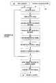
- FinFET layout generation system 10generally comprises computer 12 and program code 28 .
- User 26can interact with computer 12 and program code 28 to generate a FinFET layout 44 .
- Computer 12generally comprises memory 14 , central processing unit (CPU) 16 , input/output (I/O) interfaces 18 and bus 20 .
- a database 24may also be provided for storage of data relative to processing tasks.
- Memory 14 (and database 24 )may comprise any known type of data storage and/or transmission media, including magnetic media, optical media, random access memory (RAM), read-only memory (ROM), a data cache, a data object, etc.
- RAMrandom access memory
- ROMread-only memory
- memory 14 (and database 24 )may reside at a single physical location, comprising one or more types of data storage, or be distributed across a plurality of physical systems in various forms.
- CPU 16may comprise a single processing unit, or be distributed across one or more processing units in one or more locations, e.g., on a client and server.
- a server computertypically comprises an advanced mid-range multiprocessor-based server, such as the RS6000 from IBM, utilizing standard operating system software, which is designed to drive the operation of the particular hardware and which is compatible with other system components and I/O controllers.
- I/O interfaces 18may comprise any system for exchanging information with one or more external devices 22 .
- external devices 22may comprise any known type of input/output device including any number of a network system, modem, keyboard, mouse, scanner, voice recognition system, cathode-ray tube (CRT), liquid-crystal display (LCD), printer, disc drives, etc.
- Bus 20provides a communication link between each of the components in computer 12 and likewise may comprise any known type of transmission link, including electrical, optical, wireless, etc.
- additional componentssuch as cache memory, communication systems, system software, etc., may be incorporated into computer 12 .
- FinFET layout generation system 10receives an FET layout 40 and design constraints 42 .
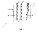
- FIG. 2depicts a portion of an exemplary FET layout 40 .
- FET layout 40includes data that defines at least one FET 45 and one or more polysilicon lines 46 .
- FET 45can include one or more gates 48 and an active area 50 .
- Gates 48can be identified as an intersection of active area 50 and polysilicon lines 46 .
- active area 50can act as a source or drain for current passing through polysilicon lines 46 .
- program code 28is shown including location system 30 .
- location system 30locates gates 48 in FET layout 40 .
- Gates 48can be found by first determining an active area 50 and polysilicon lines 46 in FET layout 40 . Gates 48 can then be identified as an intersection of active area 50 and polysilicon lines 46 .
- Location system 30can also find a gate axis 52 .
- gate axis 52can be a long edge of a particular gate 48 .
- Gate axis 52can be used by generation system 32 when generating the set of FinFET shapes as discussed in further detail below.
- FIG. 1also shows program code 28 including generation system 32 for generating a set of FinFET shapes coincident with gate(s) 48 .
- FIGS. 3 - 5depict exemplary steps of generating the set of FinFET shapes according to one aspect of the invention.
- FET layout 40includes gates 48 .
- the exemplary implementation of the inventionlimits the placement of FinFET shapes to rectangular region(s) 54 of gate(s) 48 . Consequently, after locating each gate 48 , rectangular regions 54 within each gate 48 are identified.
- gate 48 Aincludes two rectangular regions 54 A, 54 B connected by angled region 56 .
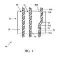
- FIG. 4depicts a next step in this exemplary implementation.
- FinFET shape 58 Acan be placed on gate 48 A.
- the size and/or location of each FinFET shape 58can be determined by one or more design constraint(s) 42 (FIG. 1) and/or the size of a corresponding polysilicon line 46 and active area 50 .
- each FinFET shape 58can be placed on rectangular region 54 .
- FinFET shapes 58can be placed anywhere on gate 48 , including, for example, angled region 56 .
- each additional FinFET shape 58can be similarly placed on gate 48 (rectangular region 54 ) at least a predetermined distance from every other FinFET shape 58 on gate 48 (rectangular region 54 ).
- FinFET shape 58 Acan be placed at a location on rectangular region 54 A.
- Gate axis 52 of gate 48 Acan be used to determine the location of subsequent FinFET shapes 58 , for example, by providing a direction to move from FinFET shape 58 A and defining a total distance within which FinFET shapes 58 will be placed.
- a set of FinFET shapes 58 for gate 48 Ais complete when no additional FinFET shape 58 can be placed on gate 48 A (rectangular regions 54 A, 54 B) at least a predetermined distance from every other FinFET shape 58 on gate 48 A (rectangular regions 54 A, 54 B).
- the methodis repeated for each gate 48 and/or each rectangular region 54 in FET layout 40 .
- each set of FinFET shapes 58can be stretched perpendicular to a corresponding gate axis 52 .
- FIG. 5depicts sets of FinFET shapes 58 after being stretched perpendicular to gate axes 52 .
- each FinFET shape 58was stretched outward from gate axes 52 (long edges) on both sides of corresponding gate 48 .
- the amount that each FinFET shape 58 is stretchedcan be determined by one or more design constraint(s) 42 (FIG. 1), active area 50 and/or polysilicon line 46 .
- FIG. 5depicts the final set of FinFET shapes 58 located so that corresponding gates 48 pass substantially near the center of each FinFET shape 58 .
- gates 48can pass substantially closer to one end of each FinFET shape 58 .
- FinFET shapes 58are described as being placed and stretched, it is understood that FinFET shapes 58 of a desired size can be appropriately located without requiring the stretching step.
- the methoddescribes locating each gate 48 , placing each FinFET shape 58 and stretching each FinFET shape 58 , it is understood that each of the steps can be fully performed for one or more FinFET shapes 58 , for example, without having found all gates 48 .
- the inventioncan further include modification system 34 .
- Modification system 34can create a FinFET layout by modifying the FET layout to include the set of FinFET shapes.
- FIGS. 6 - 8depict exemplary steps for generating a FinFET layout according to one aspect of the invention.
- a removal area 60can be defined in FET layout 40 .
- Removal area 60represents a portion of active area 50 to be replaced by set(s) of FinFET shapes 58 .
- removal area 60can initially be defined as a portion of active area 50 that corresponds to a particular gate 48 (FIG. 2).
- Removal area 60can be stretched perpendicular to gate axis 52 (FIG. 2) in a substantially similar fashion as described above with reference to FinFET shapes.
- removal area 60can be initially defined as the desired area, without requiring the stretching step.
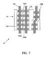
- FIG. 7depicts a portion of a FinFET layout 44 as it is created from FET layout 40 (FIG. 6).
- FinFET layout 44is shown having a FinFET device 61 , including an active area 150 , sets of FinFET shapes 158 , 158 A, 158 B and polysilicon lines 146 .
- Active area 150is created from active area 50 of FIG. 6 by removing each removal area 60 .
- Set(s) of FinFET shapes 158 , 158 A, 158 Bare then added to active area 150 .
- active area 150includes area(s) defined by the set(s) of FinFET shapes 158 , 158 A, 158 B.
- active area 150may require adjusting to conform with a set of design constraints 42 (FIG. 1).
- Design constraint(s) 42can include, for example, a minimum width and a minimum spacing. These values can be determined by electrical and/or lithographic constraints of the manufacturing process. As a result of the previous steps, active area 150 may have a portion that is narrower than a minimum width. Similarly, a gap may be present within active area 150 that is narrower than the minimum spacing.
- program code 28can further include adjustment system 36 for adjusting an active area in a FinFET layout to conform with a set of design constraints 42 .
- design constraints 42includes a minimum width and minimum spacing and that these constraints are substantially the same distance.
- portions 62 A, 62 B of active area 150are narrower than the minimum width.
- Adjustment system 36removes portions 62 A, 62 B of active area 150 .
- FIG. 8depicts a portion of an exemplary FinFET layout 44 after each step has been performed. Active area 150 is shown with portions 62 A, 62 B (FIG. 7) removed, and additional areas added to fill the resulting gaps.
- FIG. 9depicts a FinFET layout generation method according to one aspect of the invention.
- a gateis located in FET layout 40 in step S 1 .
- the gatemay be defined by an intersection of a polysilicon line with an active area as described above.
- a gate axis for the gateis determined in step S 2 .
- a set of FinFET shapescan then be generated in step S 3 that are coincident with the gate, and in step S 4 , each of the FinFET shapes is stretched by a predetermined amount in a direction perpendicular to the gate axis.
- the generation of the FinFET shapescan be partially determined by one or more of design constraints 42 .
- a removal area of the active areais defined. Initially, this can be defined as a portion of the active area that corresponds to the gate.
- the removal areais stretched in step S 6 in a manner similar to the FinFET shapes.
- the removal areais then removed from the active area in step S 7 .
- step S 8adjusts the active area to conform with the set of design constraints 42 . This results in a completed FinFET layout 44 .
- steps S 1 and S 5can be performed in parallel (for example, steps S 1 and S 5 ), and/or the order of the steps can be modified. Additionally, steps can be merged and/or dropped. For example, steps S 1 and S 5 can be merged, while step S 4 can be dropped if the initial set of FinFET shapes is the desired size.
- Computer program, software program, program, program product, or softwarein the present context mean any expression, in any language, code or notation, of a set of instructions intended to cause a system having an information processing capability to perform a particular function either directly or after the following: (a) conversion to another language, code or notation; and/or (b) reproduction in a different material form.
Landscapes
- Engineering & Computer Science (AREA)
- Computer Hardware Design (AREA)
- Physics & Mathematics (AREA)
- Theoretical Computer Science (AREA)
- Evolutionary Computation (AREA)
- Geometry (AREA)
- General Engineering & Computer Science (AREA)
- General Physics & Mathematics (AREA)
- Design And Manufacture Of Integrated Circuits (AREA)
- Metal-Oxide And Bipolar Metal-Oxide Semiconductor Integrated Circuits (AREA)
- Insulated Gate Type Field-Effect Transistor (AREA)
Abstract
Description
- 1. Technical Field[0001]
- The invention generally relates to field effect transistor (FET) and three-dimensional FET (FinFET) layouts. Specifically, the invention generates a set of FinFET shapes by analyzing an FET layout. Further, a FinFET layout can be created by modifying the FET layout to include the set of FinFET shapes. The FinFET layout can be further modified to comply with electrical and/or design constraints.[0002]
- 2. Related Art[0003]
- In the generation of layouts for electronic devices, an FET can typically be defined by a silicon active area that intersects with one or more polysilicon lines. The silicon active area is often a two-dimensional, planar layer of silicon. Recent advances allow the planar layer to be replaced by a three-dimensional layer of silicon to create what is commonly referred to as a FinFET.[0004]
- A FinFET is a double gate FET with a fully depleted body that provides several advantages over a conventional FET. These advantages include nearly ideal turn off in sub-threshold voltages, giving lower off-currents and/or allowing lower threshold voltages, no loss to drain currents from body effects, no ‘floating’ body effects (often associated with some Silicon on Insulator (SOI) FETs), higher current density, lower voltage operation, and reduced short channel degradation of threshold voltage and off current. Furthermore, FinFETs are more easily scaled to smaller physical dimensions and lower operating voltages than conventional and SOI FETs.[0005]
- Frequently, an FET layout is created by incorporating shapes that represent the desired shape of silicon active areas and polysilicon lines. Once created, the FET layout is used to generate an active area mask. Using the active area mask, the correct active area can then be applied. Several constraints limit the application process. For example, an active area must have a minimal width and a minimal amount of space must be left between active areas.[0006]
- Numerous software products exist that allow for the relatively easy design of an FET layout including, for example, IBM's Niagara, Avant!®, Metrographics and Cadence®. However, no solutions currently exist for generating a FinFET layout.[0007]
- As a result, there exists a need to generate a set of FinFET shapes based on an FET layout. Further, a need exists to create a FinFET layout by modifying an FET layout to include a set of FinFET shapes. Further, a need exists to ensure that a FinFET layout conforms with electrical and/or design constraints.[0008]
- The invention generates a set of FinFET shapes using an FET layout. The invention can further create a FinFET layout by modifying the FET layout to include the set of FinFET shapes. The invention can also modify an active area in a FinFET layout to conform with electrical and/or design constraints.[0009]
- A first aspect of the invention provides a method for generating a set of FinFET shapes, comprising: locating a gate in an FET layout; finding a gate axis of the gate; generating the set of FinFET shapes coincident with the gate; and stretching the set of FinFET shapes perpendicular to the gate axis.[0010]
- A second aspect of the invention provides a computer program product comprising a computer useable medium having computer readable program code embodied therein for generating a set of FinFET shapes, the program product comprising: program code for locating a gate in an FET layout; program code for finding a gate axis of the gate; program code for generating the set of FinFET shapes coincident with the gate; and program code for stretching the set of FinFET shapes perpendicular to the gate axis.[0011]
- A third aspect of the invention provides a system for generating a set of FinFET shapes, comprising: a location system for locating a gate in an FET layout; and a generation system for generating a set of FinFET shapes coincident with the gate.[0012]
- The exemplary aspects of the present invention are designed to solve the problems herein described and other problems not discussed, which are discoverable by a skilled artisan.[0013]
- These and other features and advantages of this invention will be more readily understood from the following detailed description of the various aspects of the invention taken in conjunction with the accompanying drawings in which:[0014]
- FIG. 1 depicts a system according to one aspect of the invention;[0015]
- FIG. 2 depicts a portion of an exemplary FET layout;[0016]
- FIG. 3 depicts an exemplary step for generating a set of FinFET shapes according to one aspect of the invention;[0017]
- FIG. 4 depicts an exemplary step for generating a set of FinFET shapes according to one aspect of the invention;[0018]
- FIG. 5 depicts an exemplary step for generating a set of FinFET shapes according to one aspect of the invention;[0019]
- FIG. 6 depicts an exemplary step for generating a FinFET layout according to one aspect of the invention;[0020]
- FIG. 7 depicts a portion of a FinFET layout as it is created from an FET layout according to one aspect of the invention;[0021]
- FIG. 8 depicts a portion of an exemplary FinFET layout according to one aspect of the invention; and[0022]
- FIG. 9 depicts a FinFET layout generation method according to one aspect of the invention.[0023]
- It is noted that the drawings of the invention are not to scale. The drawings are intended to depict only typical aspects of the invention, and therefore should not be considered as limiting the scope of the invention. In the drawings, like numbering represents like elements between the drawings.[0024]
- The invention provides a method for generating a set of FinFET shapes that partially define a FinFET. The method analyzes an FET layout (data that defines a layout for an electronic device including at least one FET) to generate the set of FinFET shapes by locating a gate in the FET layout and generating the set of FinFET shapes coincident with the gate. The invention further provides a method and system for creating a FinFET layout (data that defines a layout for an electronic device including at least one FinFET) from an FET layout by modifying the FET layout to include the set of FinFET shapes.[0025]
- Turning to FIG. 1, a FinFET[0026]
layout generation system 10 according to one aspect of the invention is depicted. FinFETlayout generation system 10 generally comprisescomputer 12 andprogram code 28.User 26 can interact withcomputer 12 andprogram code 28 to generate aFinFET layout 44. - [0027]
Computer 12 generally comprisesmemory 14, central processing unit (CPU)16, input/output (I/O)interfaces 18 andbus 20. Adatabase 24 may also be provided for storage of data relative to processing tasks. Memory14 (and database24) may comprise any known type of data storage and/or transmission media, including magnetic media, optical media, random access memory (RAM), read-only memory (ROM), a data cache, a data object, etc. Moreover, memory14 (and database24) may reside at a single physical location, comprising one or more types of data storage, or be distributed across a plurality of physical systems in various forms.CPU 16 may comprise a single processing unit, or be distributed across one or more processing units in one or more locations, e.g., on a client and server. A server computer typically comprises an advanced mid-range multiprocessor-based server, such as the RS6000 from IBM, utilizing standard operating system software, which is designed to drive the operation of the particular hardware and which is compatible with other system components and I/O controllers. I/O interfaces 18 may comprise any system for exchanging information with one or moreexternal devices 22. For example,external devices 22 may comprise any known type of input/output device including any number of a network system, modem, keyboard, mouse, scanner, voice recognition system, cathode-ray tube (CRT), liquid-crystal display (LCD), printer, disc drives, etc.Bus 20 provides a communication link between each of the components incomputer 12 and likewise may comprise any known type of transmission link, including electrical, optical, wireless, etc. In addition, although not shown, additional components, such as cache memory, communication systems, system software, etc., may be incorporated intocomputer 12. - In one embodiment, FinFET[0028]
layout generation system 10 receives anFET layout 40 anddesign constraints 42. FIG. 2 depicts a portion of anexemplary FET layout 40.FET layout 40 includes data that defines at least oneFET 45 and one or more polysilicon lines46. For example,FET 45 can include one ormore gates 48 and anactive area 50.Gates 48 can be identified as an intersection ofactive area 50 andpolysilicon lines 46. When in operation,active area 50 can act as a source or drain for current passing throughpolysilicon lines 46. - As seen in FIG. 1,[0029]
program code 28 is shown includinglocation system 30. Using FIG. 2 as an example,location system 30 locatesgates 48 inFET layout 40.Gates 48 can be found by first determining anactive area 50 andpolysilicon lines 46 inFET layout 40.Gates 48 can then be identified as an intersection ofactive area 50 andpolysilicon lines 46.Location system 30 can also find agate axis 52. For example,gate axis 52 can be a long edge of aparticular gate 48.Gate axis 52 can be used bygeneration system 32 when generating the set of FinFET shapes as discussed in further detail below. - FIG. 1 also shows[0030]
program code 28 includinggeneration system 32 for generating a set of FinFET shapes coincident with gate(s)48. FIGS.3-5 depict exemplary steps of generating the set of FinFET shapes according to one aspect of the invention. As shown in FIG. 3,FET layout 40 includesgates 48. The exemplary implementation of the invention limits the placement of FinFET shapes to rectangular region(s)54 of gate(s)48. Consequently, after locating eachgate 48,rectangular regions 54 within eachgate 48 are identified. For example,gate 48A includes tworectangular regions angled region 56. - FIG. 4 depicts a next step in this exemplary implementation. Continuing with[0031]
gate 48A as an example of the general method,FinFET shape 58A can be placed ongate 48A. The size and/or location of eachFinFET shape 58 can be determined by one or more design constraint(s)42 (FIG. 1) and/or the size of acorresponding polysilicon line 46 andactive area 50. As discussed above, eachFinFET shape 58 can be placed onrectangular region 54. Alternatively, FinFET shapes58 can be placed anywhere ongate 48, including, for example, angledregion 56. After placing aninitial FinFET shape 58 ongate 48, eachadditional FinFET shape 58 can be similarly placed on gate48 (rectangular region54) at least a predetermined distance from everyother FinFET shape 58 on gate48 (rectangular region54). Continuing to usegate 48A as an example, initially,FinFET shape 58A can be placed at a location onrectangular region 54A.Gate axis 52 ofgate 48A can be used to determine the location of subsequent FinFET shapes58, for example, by providing a direction to move fromFinFET shape 58A and defining a total distance within which FinFET shapes58 will be placed. A set of FinFET shapes58 forgate 48A is complete when noadditional FinFET shape 58 can be placed ongate 48A (rectangular regions other FinFET shape 58 ongate 48A (rectangular regions gate 48 and/or eachrectangular region 54 inFET layout 40. - Once each set of FinFET shapes[0032]58 is generated coincident with each
gate 48, each set of FinFET shapes58 can be stretched perpendicular to acorresponding gate axis 52. FIG. 5 depicts sets of FinFET shapes58 after being stretched perpendicular to gate axes52. In this example, eachFinFET shape 58 was stretched outward from gate axes52 (long edges) on both sides of correspondinggate 48. The amount that eachFinFET shape 58 is stretched can be determined by one or more design constraint(s)42 (FIG. 1),active area 50 and/orpolysilicon line 46. - FIG. 5 depicts the final set of FinFET shapes[0033]58 located so that corresponding
gates 48 pass substantially near the center of eachFinFET shape 58. Alternatively,gates 48 can pass substantially closer to one end of eachFinFET shape 58. Additionally, while FinFET shapes58 are described as being placed and stretched, it is understood that FinFET shapes58 of a desired size can be appropriately located without requiring the stretching step. Further, while the method describes locating eachgate 48, placing eachFinFET shape 58 and stretching eachFinFET shape 58, it is understood that each of the steps can be fully performed for one or more FinFET shapes58, for example, without having found allgates 48. - As shown in FIG. 1, the invention can further include[0034]
modification system 34.Modification system 34 can create a FinFET layout by modifying the FET layout to include the set of FinFET shapes. FIGS.6-8 depict exemplary steps for generating a FinFET layout according to one aspect of the invention. - As shown in FIG. 6, for example, a[0035]
removal area 60 can be defined inFET layout 40.Removal area 60 represents a portion ofactive area 50 to be replaced by set(s) of FinFET shapes58. For example,removal area 60 can initially be defined as a portion ofactive area 50 that corresponds to a particular gate48 (FIG. 2).Removal area 60 can be stretched perpendicular to gate axis52 (FIG. 2) in a substantially similar fashion as described above with reference to FinFET shapes. Alternatively, as also described above,removal area 60 can be initially defined as the desired area, without requiring the stretching step. - FIG. 7 depicts a portion of a[0036]
FinFET layout 44 as it is created from FET layout40 (FIG. 6).FinFET layout 44 is shown having aFinFET device 61, including anactive area 150, sets of FinFET shapes158,158A,158B andpolysilicon lines 146.Active area 150 is created fromactive area 50 of FIG. 6 by removing eachremoval area 60. Set(s) of FinFET shapes158,158A,158B are then added toactive area 150. As a result,active area 150 includes area(s) defined by the set(s) of FinFET shapes158,158A,158B. - However,[0037]
active area 150 may require adjusting to conform with a set of design constraints42 (FIG. 1). Design constraint(s)42 can include, for example, a minimum width and a minimum spacing. These values can be determined by electrical and/or lithographic constraints of the manufacturing process. As a result of the previous steps,active area 150 may have a portion that is narrower than a minimum width. Similarly, a gap may be present withinactive area 150 that is narrower than the minimum spacing. - As shown in FIG. 1,[0038]
program code 28 can further include adjustment system36 for adjusting an active area in a FinFET layout to conform with a set ofdesign constraints 42. Returning to FIG. 7, assume, for example, thatdesign constraints 42 includes a minimum width and minimum spacing and that these constraints are substantially the same distance. Additionally, assumeportions active area 150 are narrower than the minimum width. Adjustment system36 removesportions active area 150. However, for example, onceportion 62A is removed, a gap between FinFET shapes158A,158B (now part of active area150) is created. Consequently, adjustment system36 adds an area toactive area 150 to fill the gap. FIG. 8 depicts a portion of anexemplary FinFET layout 44 after each step has been performed.Active area 150 is shown withportions - FIG. 9 depicts a FinFET layout generation method according to one aspect of the invention. Initially, a gate is located in[0039]
FET layout 40 in step S1. The gate may be defined by an intersection of a polysilicon line with an active area as described above. Once located, a gate axis for the gate is determined in step S2. A set of FinFET shapes can then be generated in step S3 that are coincident with the gate, and in step S4, each of the FinFET shapes is stretched by a predetermined amount in a direction perpendicular to the gate axis. The generation of the FinFET shapes can be partially determined by one or more ofdesign constraints 42. - In step S[0040]5, a removal area of the active area is defined. Initially, this can be defined as a portion of the active area that corresponds to the gate. The removal area is stretched in step S6 in a manner similar to the FinFET shapes. The removal area is then removed from the active area in step S7.
- The initial steps can be repeated for one or more gates in the FET layout. Once FinFET shapes have been generated for every desired gate, the FinFET shapes can be added to the active area in step S[0041]8. Finally, step S9 adjusts the active area to conform with the set of
design constraints 42. This results in a completedFinFET layout 44. - It is understood that the method depicted in FIG. 9 is only exemplary of the methods of the invention. Each step is shown in a linear fashion for clarity. Steps may be performed in parallel (for example, steps S[0042]1 and S5), and/or the order of the steps can be modified. Additionally, steps can be merged and/or dropped. For example, steps S1 and S5 can be merged, while step S4 can be dropped if the initial set of FinFET shapes is the desired size.
- In the previous discussion, it will be understood that the method steps discussed can be performed by a processor, such as[0043]
CPU 16 ofcomputer 12, executing instructions of a program product (such as program product28) stored inmemory 14. It is understood that the various devices, modules, mechanisms and systems described herein may be realized in hardware, software, or a combination of hardware and software, and may be compartmentalized other than as shown. They may be implemented by any type of computer system or other apparatus adapted for carrying out the methods described herein. A typical combination of hardware and software could be a general-purpose computer system with a computer program that, when loaded and executed, controls the computer system such that it carries out the methods described herein. Alternatively, a specific use computer, containing specialized hardware for carrying out one or more of the functional tasks of the invention could be utilized. The present invention can also be embedded in a computer program product, which comprises all the features enabling the implementation of the methods and functions described herein, and which, when loaded in a computer system, is able to carry out these methods and functions. Computer program, software program, program, program product, or software, in the present context mean any expression, in any language, code or notation, of a set of instructions intended to cause a system having an information processing capability to perform a particular function either directly or after the following: (a) conversion to another language, code or notation; and/or (b) reproduction in a different material form. - The foregoing description of various aspects of the invention has been presented for purposes of illustration and description. It is not intended to be exhaustive or to limit the invention to the precise form disclosed, and obviously, many modifications and variations are possible. Such modifications and variations that may be apparent to a person skilled in the art are intended to be included within the scope of the invention as defined by the accompanying claims.[0044]
Claims (21)
Priority Applications (3)
| Application Number | Priority Date | Filing Date | Title |
|---|---|---|---|
| US09/683,631US6662350B2 (en) | 2002-01-28 | 2002-01-28 | FinFET layout generation |
| JP2003008671AJP4056398B2 (en) | 2002-01-28 | 2003-01-16 | Method, program and system for generating FinFET shapes |
| TW092101826ATW584963B (en) | 2002-01-28 | 2003-01-28 | FinFET layout generation |
Applications Claiming Priority (1)
| Application Number | Priority Date | Filing Date | Title |
|---|---|---|---|
| US09/683,631US6662350B2 (en) | 2002-01-28 | 2002-01-28 | FinFET layout generation |
Publications (2)
| Publication Number | Publication Date |
|---|---|
| US20030145299A1true US20030145299A1 (en) | 2003-07-31 |
| US6662350B2 US6662350B2 (en) | 2003-12-09 |
Family
ID=27613756
Family Applications (1)
| Application Number | Title | Priority Date | Filing Date |
|---|---|---|---|
| US09/683,631Expired - Fee RelatedUS6662350B2 (en) | 2002-01-28 | 2002-01-28 | FinFET layout generation |
Country Status (3)
| Country | Link |
|---|---|
| US (1) | US6662350B2 (en) |
| JP (1) | JP4056398B2 (en) |
| TW (1) | TW584963B (en) |
Cited By (51)
| Publication number | Priority date | Publication date | Assignee | Title |
|---|---|---|---|---|
| US20060216881A1 (en)* | 2005-03-25 | 2006-09-28 | Hynix Semiconductor Inc. | Method for manufacturing semiconductor device |
| US20070094628A1 (en)* | 2005-10-26 | 2007-04-26 | Freescale Semiconductor, Inc. | Methods of generating planar double gate transistor shapes and data processing system readable media to perform the methods |
| US20070093029A1 (en)* | 2005-10-26 | 2007-04-26 | Freescale Semiconductor, Inc. | Methods of generating planar double gate transistor shapes and data processing system readable media to perform the methods |
| WO2007059734A1 (en)* | 2005-11-21 | 2007-05-31 | Infineon Technologies Ag | Multi-fin component arrangement and method for producing a multi-fin component arrangement |
| US20080263492A1 (en)* | 2007-04-18 | 2008-10-23 | Harry Chuang | 3-Dimensional Device Design Layout |
| US20080296691A1 (en)* | 2007-05-30 | 2008-12-04 | Harry Chuang | Layout methods of integrated circuits having unit MOS devices |
| EP1548619A3 (en)* | 2003-12-22 | 2009-05-13 | International Business Machines Corporation | Method and device for automated layer generation for double-gate finFET designs |
| US20100187622A1 (en)* | 2008-03-13 | 2010-07-29 | Tela Innovations, Inc. | Linear Gate Level Cross-Coupled Transistor Device with Complimentary Pairs of Cross-Coupled Transistors Defined by Physically Separate Gate Electrodes within Gate Electrode Level |
| US20100287518A1 (en)* | 2009-05-06 | 2010-11-11 | Tela Innovations, Inc. | Cell Circuit and Layout with Linear Finfet Structures |
| US20110024794A1 (en)* | 2009-07-31 | 2011-02-03 | Taiwan Semiconductor Manufacturing Company, Ltd. | Fin structure for high mobility multiple-gate transistor |
| US20110233679A1 (en)* | 2010-03-25 | 2011-09-29 | Taiwan Semiconductor Manufacturing Company, Ltd. | Integrated circuit including finfets and methods for forming the same |
| US20110282478A1 (en)* | 2010-05-14 | 2011-11-17 | Taiwan Semiconductor Manufacturing Company, Ltd. | Finfet boundary optimization |
| US20110283245A1 (en)* | 2010-05-14 | 2011-11-17 | Taiwan Semiconductor Manufacturing Company, Ltd. | Automatic layout conversion for finfet device |
| US8129756B2 (en) | 2006-03-09 | 2012-03-06 | Tela Innovations, Inc. | Integrated circuit including at least six linear-shaped conductive structures forming gate electrodes of transistors with at least two different extension distances beyond conductive contacting structures |
| US20120124528A1 (en)* | 2010-11-12 | 2012-05-17 | Taiwan Semiconductor Manufacturing Company, Ltd. | Method and device for increasing fin device density for unaligned fins |
| US8214778B2 (en) | 2007-08-02 | 2012-07-03 | Tela Innovations, Inc. | Methods for cell phasing and placement in dynamic array architecture and implementation of the same |
| US8225239B2 (en) | 2006-03-09 | 2012-07-17 | Tela Innovations, Inc. | Methods for defining and utilizing sub-resolution features in linear topology |
| US8225261B2 (en) | 2006-03-09 | 2012-07-17 | Tela Innovations, Inc. | Methods for defining contact grid in dynamic array architecture |
| US8245180B2 (en) | 2006-03-09 | 2012-08-14 | Tela Innovations, Inc. | Methods for defining and using co-optimized nanopatterns for integrated circuit design and apparatus implementing same |
| US8247846B2 (en) | 2006-03-09 | 2012-08-21 | Tela Innovations, Inc. | Oversized contacts and vias in semiconductor chip defined by linearly constrained topology |
| US8283701B2 (en) | 2007-08-02 | 2012-10-09 | Tela Innovations, Inc. | Semiconductor device with dynamic array sections defined and placed according to manufacturing assurance halos |
| US8286107B2 (en) | 2007-02-20 | 2012-10-09 | Tela Innovations, Inc. | Methods and systems for process compensation technique acceleration |
| US20120278781A1 (en)* | 2011-04-29 | 2012-11-01 | Taiwan Semiconductor Manufacturing Company, Ltd. | System and methods for converting planar design to finfet design |
| US8431453B2 (en) | 2011-03-31 | 2013-04-30 | Taiwan Semiconductor Manufacturing Company, Ltd. | Plasma doping to reduce dielectric loss during removal of dummy layers in a gate structure |
| US8448102B2 (en) | 2006-03-09 | 2013-05-21 | Tela Innovations, Inc. | Optimizing layout of irregular structures in regular layout context |
| US8453094B2 (en) | 2008-01-31 | 2013-05-28 | Tela Innovations, Inc. | Enforcement of semiconductor structure regularity for localized transistors and interconnect |
| US8471391B2 (en) | 2008-03-27 | 2013-06-25 | Tela Innovations, Inc. | Methods for multi-wire routing and apparatus implementing same |
| US8541879B2 (en) | 2007-12-13 | 2013-09-24 | Tela Innovations, Inc. | Super-self-aligned contacts and method for making the same |
| US8653857B2 (en) | 2006-03-09 | 2014-02-18 | Tela Innovations, Inc. | Circuitry and layouts for XOR and XNOR logic |
| US8661392B2 (en) | 2009-10-13 | 2014-02-25 | Tela Innovations, Inc. | Methods for cell boundary encroachment and layouts implementing the Same |
| US8658542B2 (en) | 2006-03-09 | 2014-02-25 | Tela Innovations, Inc. | Coarse grid design methods and structures |
| US8667443B2 (en) | 2007-03-05 | 2014-03-04 | Tela Innovations, Inc. | Integrated circuit cell library for multiple patterning |
| US8680626B2 (en) | 2007-10-26 | 2014-03-25 | Tela Innovations, Inc. | Methods, structures, and designs for self-aligning local interconnects used in integrated circuits |
| US8809940B2 (en) | 2010-10-13 | 2014-08-19 | Taiwan Semiconductor Manufacturing Company, Ltd. | Fin held effect transistor |
| US8839175B2 (en) | 2006-03-09 | 2014-09-16 | Tela Innovations, Inc. | Scalable meta-data objects |
| US8863063B2 (en) | 2009-05-06 | 2014-10-14 | Tela Innovations, Inc. | Finfet transistor circuit |
| US8980719B2 (en) | 2010-04-28 | 2015-03-17 | Taiwan Semiconductor Manufacturing Company, Ltd. | Methods for doping fin field-effect transistors |
| US9035359B2 (en) | 2006-03-09 | 2015-05-19 | Tela Innovations, Inc. | Semiconductor chip including region including linear-shaped conductive structures forming gate electrodes and having electrical connection areas arranged relative to inner region between transistors of different types and associated methods |
| CN104809262A (en)* | 2014-01-24 | 2015-07-29 | 格罗方德半导体公司 | Method and apparatus for modified cell architecture and the resulting device |
| US9122832B2 (en) | 2008-08-01 | 2015-09-01 | Tela Innovations, Inc. | Methods for controlling microloading variation in semiconductor wafer layout and fabrication |
| US9159627B2 (en) | 2010-11-12 | 2015-10-13 | Tela Innovations, Inc. | Methods for linewidth modification and apparatus implementing the same |
| US9230910B2 (en) | 2006-03-09 | 2016-01-05 | Tela Innovations, Inc. | Oversized contacts and vias in layout defined by linearly constrained topology |
| US9704862B2 (en) | 2014-09-18 | 2017-07-11 | Samsung Electronics Co., Ltd. | Semiconductor devices and methods for manufacturing the same |
| US9767248B2 (en) | 2014-09-18 | 2017-09-19 | Samsung Electronics, Co., Ltd. | Semiconductor having cross coupled structure and layout verification method thereof |
| US9811626B2 (en) | 2014-09-18 | 2017-11-07 | Samsung Electronics Co., Ltd. | Method of designing layout of semiconductor device |
| TWI628741B (en)* | 2014-07-22 | 2018-07-01 | 三星電子股份有限公司 | Integrated circuit, integrated circuit based semiconductor component and standard cell library |
| US10026661B2 (en) | 2014-09-18 | 2018-07-17 | Samsung Electronics Co., Ltd. | Semiconductor device for testing large number of devices and composing method and test method thereof |
| US10095825B2 (en) | 2014-09-18 | 2018-10-09 | Samsung Electronics Co., Ltd. | Computer based system for verifying layout of semiconductor device and layout verify method thereof |
| US11289483B2 (en)* | 2016-12-23 | 2022-03-29 | Intel Corporation | Metal fuse and self-aligned gate edge (SAGE) architecture having a metal fuse |
| US11314915B2 (en) | 2019-09-03 | 2022-04-26 | Samsung Electronics Co., Ltd. | Methods of designing layouts of semiconductor devices |
| US11430893B2 (en) | 2020-07-10 | 2022-08-30 | Taiwan Semiconductor Manufacturing Co., Ltd. | Method of manufacturing a semiconductor device and a semiconductor device |
Families Citing this family (62)
| Publication number | Priority date | Publication date | Assignee | Title |
|---|---|---|---|---|
| KR100702552B1 (en)* | 2003-12-22 | 2007-04-04 | 인터내셔널 비지네스 머신즈 코포레이션 | Automated Layer Creation Method and Device for Double Gate FFT Design |
| US7060539B2 (en)* | 2004-03-01 | 2006-06-13 | International Business Machines Corporation | Method of manufacture of FinFET devices with T-shaped fins and devices manufactured thereby |
| US7115920B2 (en)* | 2004-04-12 | 2006-10-03 | International Business Machines Corporation | FinFET transistor and circuit |
| DE102004020593A1 (en)* | 2004-04-27 | 2005-11-24 | Infineon Technologies Ag | Fin field effect transistor arrangement and method for producing a fin field effect transistor arrangement |
| US20060076547A1 (en)* | 2004-09-24 | 2006-04-13 | Mentor Graphics Corp. | Three-dimensional viewing and editing of microcircuit design |
| US7183142B2 (en)* | 2005-01-13 | 2007-02-27 | International Business Machines Corporation | FinFETs with long gate length at high density |
| US20070023839A1 (en)* | 2005-07-27 | 2007-02-01 | International Business Machines Corporation | Finfet gate formed of carbon nanotubes |
| US7517764B2 (en)* | 2006-06-29 | 2009-04-14 | International Business Machines Corporation | Bulk FinFET device |
| US8273617B2 (en) | 2009-09-30 | 2012-09-25 | Suvolta, Inc. | Electronic devices and systems, and methods for making and using the same |
| US8421162B2 (en) | 2009-09-30 | 2013-04-16 | Suvolta, Inc. | Advanced transistors with punch through suppression |
| US8530286B2 (en) | 2010-04-12 | 2013-09-10 | Suvolta, Inc. | Low power semiconductor transistor structure and method of fabrication thereof |
| US8569128B2 (en) | 2010-06-21 | 2013-10-29 | Suvolta, Inc. | Semiconductor structure and method of fabrication thereof with mixed metal types |
| US8759872B2 (en) | 2010-06-22 | 2014-06-24 | Suvolta, Inc. | Transistor with threshold voltage set notch and method of fabrication thereof |
| US8624320B2 (en)* | 2010-08-02 | 2014-01-07 | Advanced Micro Devices, Inc. | Process for forming fins for a FinFET device |
| US8659072B2 (en) | 2010-09-24 | 2014-02-25 | Taiwan Semiconductor Manufacturing Company, Ltd. | Series FinFET implementation schemes |
| US8404551B2 (en) | 2010-12-03 | 2013-03-26 | Suvolta, Inc. | Source/drain extension control for advanced transistors |
| US8461875B1 (en) | 2011-02-18 | 2013-06-11 | Suvolta, Inc. | Digital circuits having improved transistors, and methods therefor |
| US8525271B2 (en) | 2011-03-03 | 2013-09-03 | Suvolta, Inc. | Semiconductor structure with improved channel stack and method for fabrication thereof |
| US8400219B2 (en) | 2011-03-24 | 2013-03-19 | Suvolta, Inc. | Analog circuits having improved transistors, and methods therefor |
| US8748270B1 (en) | 2011-03-30 | 2014-06-10 | Suvolta, Inc. | Process for manufacturing an improved analog transistor |
| US8796048B1 (en) | 2011-05-11 | 2014-08-05 | Suvolta, Inc. | Monitoring and measurement of thin film layers |
| US8999861B1 (en) | 2011-05-11 | 2015-04-07 | Suvolta, Inc. | Semiconductor structure with substitutional boron and method for fabrication thereof |
| US8811068B1 (en) | 2011-05-13 | 2014-08-19 | Suvolta, Inc. | Integrated circuit devices and methods |
| US8569156B1 (en) | 2011-05-16 | 2013-10-29 | Suvolta, Inc. | Reducing or eliminating pre-amorphization in transistor manufacture |
| US8735987B1 (en) | 2011-06-06 | 2014-05-27 | Suvolta, Inc. | CMOS gate stack structures and processes |
| US8995204B2 (en) | 2011-06-23 | 2015-03-31 | Suvolta, Inc. | Circuit devices and methods having adjustable transistor body bias |
| US8629016B1 (en) | 2011-07-26 | 2014-01-14 | Suvolta, Inc. | Multiple transistor types formed in a common epitaxial layer by differential out-diffusion from a doped underlayer |
| US8748986B1 (en) | 2011-08-05 | 2014-06-10 | Suvolta, Inc. | Electronic device with controlled threshold voltage |
| KR101891373B1 (en) | 2011-08-05 | 2018-08-24 | 엠아이이 후지쯔 세미컨덕터 리미티드 | Semiconductor devices having fin structures and fabrication methods thereof |
| US8614128B1 (en) | 2011-08-23 | 2013-12-24 | Suvolta, Inc. | CMOS structures and processes based on selective thinning |
| US8645878B1 (en) | 2011-08-23 | 2014-02-04 | Suvolta, Inc. | Porting a circuit design from a first semiconductor process to a second semiconductor process |
| US8713511B1 (en) | 2011-09-16 | 2014-04-29 | Suvolta, Inc. | Tools and methods for yield-aware semiconductor manufacturing process target generation |
| US9236466B1 (en) | 2011-10-07 | 2016-01-12 | Mie Fujitsu Semiconductor Limited | Analog circuits having improved insulated gate transistors, and methods therefor |
| US8895327B1 (en) | 2011-12-09 | 2014-11-25 | Suvolta, Inc. | Tipless transistors, short-tip transistors, and methods and circuits therefor |
| US8819603B1 (en) | 2011-12-15 | 2014-08-26 | Suvolta, Inc. | Memory circuits and methods of making and designing the same |
| US8883600B1 (en) | 2011-12-22 | 2014-11-11 | Suvolta, Inc. | Transistor having reduced junction leakage and methods of forming thereof |
| US8599623B1 (en) | 2011-12-23 | 2013-12-03 | Suvolta, Inc. | Circuits and methods for measuring circuit elements in an integrated circuit device |
| AU2013207719B2 (en)* | 2012-01-13 | 2016-02-25 | Tela Innovations, Inc. | Circuits with linear finfet structures |
| US8970289B1 (en) | 2012-01-23 | 2015-03-03 | Suvolta, Inc. | Circuits and devices for generating bi-directional body bias voltages, and methods therefor |
| US8877619B1 (en) | 2012-01-23 | 2014-11-04 | Suvolta, Inc. | Process for manufacture of integrated circuits with different channel doping transistor architectures and devices therefrom |
| US9093550B1 (en) | 2012-01-31 | 2015-07-28 | Mie Fujitsu Semiconductor Limited | Integrated circuits having a plurality of high-K metal gate FETs with various combinations of channel foundation structure and gate stack structure and methods of making same |
| US9406567B1 (en) | 2012-02-28 | 2016-08-02 | Mie Fujitsu Semiconductor Limited | Method for fabricating multiple transistor devices on a substrate with varying threshold voltages |
| US8863064B1 (en) | 2012-03-23 | 2014-10-14 | Suvolta, Inc. | SRAM cell layout structure and devices therefrom |
| US8689166B2 (en) | 2012-04-25 | 2014-04-01 | International Business Machines Corporation | Modeling the total parasitic resistances of the source/drain regions of a multi-fin multi-gate field effect transistor |
| KR101937851B1 (en)* | 2012-06-27 | 2019-04-10 | 삼성전자 주식회사 | Semiconductor integrated circuit, method of designing the same, and method of fabricating the same |
| US9299698B2 (en) | 2012-06-27 | 2016-03-29 | Mie Fujitsu Semiconductor Limited | Semiconductor structure with multiple transistors having various threshold voltages |
| US8637955B1 (en) | 2012-08-31 | 2014-01-28 | Suvolta, Inc. | Semiconductor structure with reduced junction leakage and method of fabrication thereof |
| US9112057B1 (en) | 2012-09-18 | 2015-08-18 | Mie Fujitsu Semiconductor Limited | Semiconductor devices with dopant migration suppression and method of fabrication thereof |
| US9041126B2 (en) | 2012-09-21 | 2015-05-26 | Mie Fujitsu Semiconductor Limited | Deeply depleted MOS transistors having a screening layer and methods thereof |
| US9431068B2 (en) | 2012-10-31 | 2016-08-30 | Mie Fujitsu Semiconductor Limited | Dynamic random access memory (DRAM) with low variation transistor peripheral circuits |
| US8816754B1 (en) | 2012-11-02 | 2014-08-26 | Suvolta, Inc. | Body bias circuits and methods |
| US9093997B1 (en) | 2012-11-15 | 2015-07-28 | Mie Fujitsu Semiconductor Limited | Slew based process and bias monitors and related methods |
| US9070477B1 (en) | 2012-12-12 | 2015-06-30 | Mie Fujitsu Semiconductor Limited | Bit interleaved low voltage static random access memory (SRAM) and related methods |
| US9112484B1 (en) | 2012-12-20 | 2015-08-18 | Mie Fujitsu Semiconductor Limited | Integrated circuit process and bias monitors and related methods |
| US9268885B1 (en) | 2013-02-28 | 2016-02-23 | Mie Fujitsu Semiconductor Limited | Integrated circuit device methods and models with predicted device metric variations |
| US9299801B1 (en) | 2013-03-14 | 2016-03-29 | Mie Fujitsu Semiconductor Limited | Method for fabricating a transistor device with a tuned dopant profile |
| US9478571B1 (en) | 2013-05-24 | 2016-10-25 | Mie Fujitsu Semiconductor Limited | Buried channel deeply depleted channel transistor |
| US9431383B2 (en) | 2014-07-22 | 2016-08-30 | Samsung Electronics Co., Ltd. | Integrated circuit, semiconductor device based on integrated circuit, and standard cell library |
| US9652580B2 (en) | 2014-07-23 | 2017-05-16 | Samsung Electronics Co., Ltd. | Integrated circuit layout design system and method |
| US9710006B2 (en) | 2014-07-25 | 2017-07-18 | Mie Fujitsu Semiconductor Limited | Power up body bias circuits and methods |
| KR20160013698A (en) | 2014-07-28 | 2016-02-05 | 삼성전자주식회사 | Layout design system, method of layout design and computer-readable recording medium comprising program for performing method of layout design |
| US9319013B2 (en) | 2014-08-19 | 2016-04-19 | Mie Fujitsu Semiconductor Limited | Operational amplifier input offset correction with transistor threshold voltage adjustment |
Family Cites Families (2)
| Publication number | Priority date | Publication date | Assignee | Title |
|---|---|---|---|---|
| US5097422A (en)* | 1986-10-10 | 1992-03-17 | Cascade Design Automation Corporation | Method and apparatus for designing integrated circuits |
| US6413802B1 (en)* | 2000-10-23 | 2002-07-02 | The Regents Of The University Of California | Finfet transistor structures having a double gate channel extending vertically from a substrate and methods of manufacture |
- 2002
- 2002-01-28USUS09/683,631patent/US6662350B2/ennot_activeExpired - Fee Related
- 2003
- 2003-01-16JPJP2003008671Apatent/JP4056398B2/ennot_activeExpired - Fee Related
- 2003-01-28TWTW092101826Apatent/TW584963B/ennot_activeIP Right Cessation
Cited By (205)
| Publication number | Priority date | Publication date | Assignee | Title |
|---|---|---|---|---|
| EP1548619A3 (en)* | 2003-12-22 | 2009-05-13 | International Business Machines Corporation | Method and device for automated layer generation for double-gate finFET designs |
| US20060216881A1 (en)* | 2005-03-25 | 2006-09-28 | Hynix Semiconductor Inc. | Method for manufacturing semiconductor device |
| US7396775B2 (en)* | 2005-03-25 | 2008-07-08 | Hynix Semiconductor Inc. Inc. | Method for manufacturing semiconductor device |
| US20070094628A1 (en)* | 2005-10-26 | 2007-04-26 | Freescale Semiconductor, Inc. | Methods of generating planar double gate transistor shapes and data processing system readable media to perform the methods |
| US20070093029A1 (en)* | 2005-10-26 | 2007-04-26 | Freescale Semiconductor, Inc. | Methods of generating planar double gate transistor shapes and data processing system readable media to perform the methods |
| US7491594B2 (en) | 2005-10-26 | 2009-02-17 | Freescale Semiconductor, Inc. | Methods of generating planar double gate transistor shapes |
| US7530037B2 (en) | 2005-10-26 | 2009-05-05 | Freescale Semiconductor, Inc. | Methods of generating planar double gate transistor shapes and data processing system readable media to perform the methods |
| WO2007059734A1 (en)* | 2005-11-21 | 2007-05-31 | Infineon Technologies Ag | Multi-fin component arrangement and method for producing a multi-fin component arrangement |
| US20080283925A1 (en)* | 2005-11-21 | 2008-11-20 | Joerg Berthold | Multi-Fin Component Arrangement and Method for Manufacturing a Multi-Fin Component Arrangement |
| US8217428B2 (en) | 2006-03-09 | 2012-07-10 | Tela Innovations, Inc. | Integrated circuit including gate electrode level region including at least three linear-shaped conductive structures of equal length having aligned ends and positioned at equal pitch and forming multiple gate electrodes of transistors of different type |
| US8247846B2 (en) | 2006-03-09 | 2012-08-21 | Tela Innovations, Inc. | Oversized contacts and vias in semiconductor chip defined by linearly constrained topology |
| US10186523B2 (en) | 2006-03-09 | 2019-01-22 | Tela Innovations, Inc. | Semiconductor chip having region including gate electrode features formed in part from rectangular layout shapes on gate horizontal grid and first-metal structures formed in part from rectangular layout shapes on at least eight first-metal gridlines of first-metal vertical grid |
| US10141335B2 (en) | 2006-03-09 | 2018-11-27 | Tela Innovations, Inc. | Semiconductor CIP including region having rectangular-shaped gate structures and first metal structures |
| US10141334B2 (en) | 2006-03-09 | 2018-11-27 | Tela Innovations, Inc. | Semiconductor chip including region having rectangular-shaped gate structures and first-metal structures |
| US8658542B2 (en) | 2006-03-09 | 2014-02-25 | Tela Innovations, Inc. | Coarse grid design methods and structures |
| US9917056B2 (en) | 2006-03-09 | 2018-03-13 | Tela Innovations, Inc. | Coarse grid design methods and structures |
| US9905576B2 (en) | 2006-03-09 | 2018-02-27 | Tela Innovations, Inc. | Semiconductor chip including region having rectangular-shaped gate structures and first metal structures |
| US9859277B2 (en) | 2006-03-09 | 2018-01-02 | Tela Innovations, Inc. | Methods, structures, and designs for self-aligning local interconnects used in integrated circuits |
| US9754878B2 (en) | 2006-03-09 | 2017-09-05 | Tela Innovations, Inc. | Semiconductor chip including a chip level based on a layout that includes both regular and irregular wires |
| US8129756B2 (en) | 2006-03-09 | 2012-03-06 | Tela Innovations, Inc. | Integrated circuit including at least six linear-shaped conductive structures forming gate electrodes of transistors with at least two different extension distances beyond conductive contacting structures |
| US8129755B2 (en) | 2006-03-09 | 2012-03-06 | Tela Innovations, Inc. | Integrated circuit with gate electrode level including at least four linear-shaped conductive structures of equal length and equal pitch with linear-shaped conductive structure forming one transistor |
| US8129750B2 (en) | 2006-03-09 | 2012-03-06 | Tela Innovations, Inc. | Integrated circuit including at least six linear-shaped conductive structures forming gate electrodes of transistors with at least two linear-shaped conductive structures of different length |
| US8129751B2 (en) | 2006-03-09 | 2012-03-06 | Tela Innovations, Inc. | Integrated circuit including at least six linear-shaped conductive structures forming gate electrodes and including four conductive contacting structures having at least two different connection distances |
| US8129754B2 (en) | 2006-03-09 | 2012-03-06 | Tela Innovations, Inc. | Integrated circuit with gate electrode level including at least six linear-shaped conductive structures forming gate electrodes of transisters with at least one pair of linear-shaped conductive structures having offset ends |
| US8129752B2 (en) | 2006-03-09 | 2012-03-06 | Tela Innovations, Inc. | Integrated circuit including a linear-shaped conductive structure forming one gate electrode and having length greater than or equal to one-half the length of linear-shaped conductive structure forming two gate electrodes |
| US8129757B2 (en) | 2006-03-09 | 2012-03-06 | Tela Innovations, Inc. | Integrated circuit including at least six linear-shaped conductive structive structures at equal pitch including at least two linear-shaped conductive structures having non-gate portions of different length |
| US8129819B2 (en) | 2006-03-09 | 2012-03-06 | Tela Innovations, Inc. | Method of fabricating integrated circuit including at least six linear-shaped conductive structures at equal pitch including at least two linear-shaped conductive structures having non-gate portions of different length |
| US8129753B2 (en) | 2006-03-09 | 2012-03-06 | Tela Innovations, Inc. | Integrated circuit including gate electrode level region including at least seven linear-shaped conductive structures of equal length positioned at equal pitch with at least two linear-shaped conductive structures each forming one transistor and having extending portion sized greater than gate portion |
| US8134184B2 (en) | 2006-03-09 | 2012-03-13 | Tela Innovations, Inc. | Integrated circuit having gate electrode level region including at least four linear-shaped conductive structures with some outer-contacted linear-shaped conductive structures having larger outer extending portion than inner extending portion |
| US8134183B2 (en) | 2006-03-09 | 2012-03-13 | Tela Innovations, Inc. | Integrated circuit including linear-shaped conductive structures that have gate portions and extending portions of different size |
| US8134186B2 (en) | 2006-03-09 | 2012-03-13 | Tela Innovations, Inc. | Integrated circuit including at least three linear-shaped conductive structures at equal pitch including linear-shaped conductive structure having non-gate portion length greater than gate portion length |
| US8134185B2 (en) | 2006-03-09 | 2012-03-13 | Tela Innovations, Inc. | Integrated circuit having gate electrode level region including at least seven linear-shaped conductive structures at equal pitch including linear-shaped conductive structure forming transistors of two different types and at least three linear-shaped conductive structures having aligned ends |
| US8138525B2 (en) | 2006-03-09 | 2012-03-20 | Tela Innovations, Inc. | Integrated circuit including at least three linear-shaped conductive structures of different length each forming gate of different transistor |
| US9741719B2 (en) | 2006-03-09 | 2017-08-22 | Tela Innovations, Inc. | Methods, structures, and designs for self-aligning local interconnects used in integrated circuits |
| US9711495B2 (en) | 2006-03-09 | 2017-07-18 | Tela Innovations, Inc. | Oversized contacts and vias in layout defined by linearly constrained topology |
| US8198656B2 (en) | 2006-03-09 | 2012-06-12 | Tela Innovations, Inc. | Integrated circuit including gate electrode level region including at least four linear-shaped conductive structures of equal length having aligned ends and positioned at equal pitch and forming multiple gate electrodes of transistors of different type |
| US8207053B2 (en) | 2006-03-09 | 2012-06-26 | Tela Innovations, Inc. | Electrodes of transistors with at least two linear-shaped conductive structures of different length |
| US9673825B2 (en) | 2006-03-09 | 2017-06-06 | Tela Innovations, Inc. | Circuitry and layouts for XOR and XNOR logic |
| US10230377B2 (en) | 2006-03-09 | 2019-03-12 | Tela Innovations, Inc. | Circuitry and layouts for XOR and XNOR logic |
| US8225239B2 (en) | 2006-03-09 | 2012-07-17 | Tela Innovations, Inc. | Methods for defining and utilizing sub-resolution features in linear topology |
| US8225261B2 (en) | 2006-03-09 | 2012-07-17 | Tela Innovations, Inc. | Methods for defining contact grid in dynamic array architecture |
| US8823062B2 (en) | 2006-03-09 | 2014-09-02 | Tela Innovations, Inc. | Integrated circuit with offset line end spacings in linear gate electrode level |
| US8245180B2 (en) | 2006-03-09 | 2012-08-14 | Tela Innovations, Inc. | Methods for defining and using co-optimized nanopatterns for integrated circuit design and apparatus implementing same |
| US10217763B2 (en) | 2006-03-09 | 2019-02-26 | Tela Innovations, Inc. | Semiconductor chip having region including gate electrode features of rectangular shape on gate horizontal grid and first-metal structures of rectangular shape on at least eight first-metal gridlines of first-metal vertical grid |
| US8253172B2 (en) | 2006-03-09 | 2012-08-28 | Tela Innovations, Inc. | Semiconductor device with linearly restricted gate level region including four serially connected transistors of first type and four serially connected transistors of second type separated by non-diffusion region |
| US8253173B2 (en) | 2006-03-09 | 2012-08-28 | Tela Innovations, Inc. | Semiconductor device with gate level including four transistors of first type and four transistors of second type separated by non-diffusion region and having at least two gate contacts positioned outside separating non-diffusion region |
| US8258550B2 (en) | 2006-03-09 | 2012-09-04 | Tela Innovations, Inc. | Semiconductor device including at least six transistor forming linear shapes including at least two transistor forming linear shapes having different extension distances beyond gate contact |
| US8258551B2 (en) | 2006-03-09 | 2012-09-04 | Tela Innovations, Inc. | Semiconductor device with gate level including transistors of first type and transistors of second type with corresponding gate contact placement restriction |
| US8258548B2 (en) | 2006-03-09 | 2012-09-04 | Tela Innovations, Inc. | Semiconductor device with gate level including four transistors of first type and four transistors of second type separated by non-diffusion region with restricted gate contact placement over separating non-diffusion region |
| US9589091B2 (en) | 2006-03-09 | 2017-03-07 | Tela Innovations, Inc. | Scalable meta-data objects |
| US8258552B2 (en) | 2006-03-09 | 2012-09-04 | Tela Innovations, Inc. | Semiconductor device including at least six transistor forming linear shapes with at least two transistor forming linear shapes having offset ends |
| US8258549B2 (en) | 2006-03-09 | 2012-09-04 | Tela Innovations, Inc. | Semiconductor device including two transistors of first type having gates formed by conductors of different length respectively aligned with two transistors of second type having gates formed by conductors of different length |
| US8258547B2 (en) | 2006-03-09 | 2012-09-04 | Tela Innovations, Inc. | Semiconductor device with linearly restricted gate level region including two transistors of first type and two transistors of second type with offset gate contacts |
| US8264008B2 (en) | 2006-03-09 | 2012-09-11 | Tela Innovations, Inc. | Semiconductor device including transistor forming linear shapes including gate portions and extending portions of different size |
| US8264007B2 (en) | 2006-03-09 | 2012-09-11 | Tela Innovations, Inc. | Semiconductor device including at least six transistor forming linear shapes including at least two different gate contact connection distances |
| US9443947B2 (en) | 2006-03-09 | 2016-09-13 | Tela Innovations, Inc. | Semiconductor chip including region having integrated circuit transistor gate electrodes formed by various conductive structures of specified shape and position and method for manufacturing the same |
| US8264009B2 (en) | 2006-03-09 | 2012-09-11 | Tela Innovations, Inc. | Semiconductor device with linearly restricted gate level region including four transistors of first type and four transistors of second type with gate defining shapes of different length |
| US9425272B2 (en) | 2006-03-09 | 2016-08-23 | Tela Innovations, Inc. | Semiconductor chip including integrated circuit including four transistors of first transistor type and four transistors of second transistor type with electrical connections between various transistors and methods for manufacturing the same |
| US9425145B2 (en) | 2006-03-09 | 2016-08-23 | Tela Innovations, Inc. | Oversized contacts and vias in layout defined by linearly constrained topology |
| US8653857B2 (en) | 2006-03-09 | 2014-02-18 | Tela Innovations, Inc. | Circuitry and layouts for XOR and XNOR logic |
| US8839175B2 (en) | 2006-03-09 | 2014-09-16 | Tela Innovations, Inc. | Scalable meta-data objects |
| US9425273B2 (en) | 2006-03-09 | 2016-08-23 | Tela Innovations, Inc. | Semiconductor chip including integrated circuit including at least five gate level conductive structures having particular spatial and electrical relationship and method for manufacturing the same |
| US9336344B2 (en) | 2006-03-09 | 2016-05-10 | Tela Innovations, Inc. | Coarse grid design methods and structures |
| US9240413B2 (en) | 2006-03-09 | 2016-01-19 | Tela Innovations, Inc. | Methods, structures, and designs for self-aligning local interconnects used in integrated circuits |
| US9230910B2 (en) | 2006-03-09 | 2016-01-05 | Tela Innovations, Inc. | Oversized contacts and vias in layout defined by linearly constrained topology |
| US9035359B2 (en) | 2006-03-09 | 2015-05-19 | Tela Innovations, Inc. | Semiconductor chip including region including linear-shaped conductive structures forming gate electrodes and having electrical connection areas arranged relative to inner region between transistors of different types and associated methods |
| US9009641B2 (en) | 2006-03-09 | 2015-04-14 | Tela Innovations, Inc. | Circuits with linear finfet structures |
| US8952425B2 (en) | 2006-03-09 | 2015-02-10 | Tela Innovations, Inc. | Integrated circuit including at least four linear-shaped conductive structures having extending portions of different length |
| US8436400B2 (en) | 2006-03-09 | 2013-05-07 | Tela Innovations, Inc. | Semiconductor device with gate level including gate electrode conductors for transistors of first type and transistors of second type with some gate electrode conductors of different length |
| US8448102B2 (en) | 2006-03-09 | 2013-05-21 | Tela Innovations, Inc. | Optimizing layout of irregular structures in regular layout context |
| US8946781B2 (en) | 2006-03-09 | 2015-02-03 | Tela Innovations, Inc. | Integrated circuit including gate electrode conductive structures with different extension distances beyond contact |
| US8921897B2 (en) | 2006-03-09 | 2014-12-30 | Tela Innovations, Inc. | Integrated circuit with gate electrode conductive structures having offset ends |
| US8921896B2 (en) | 2006-03-09 | 2014-12-30 | Tela Innovations, Inc. | Integrated circuit including linear gate electrode structures having different extension distances beyond contact |
| US8286107B2 (en) | 2007-02-20 | 2012-10-09 | Tela Innovations, Inc. | Methods and systems for process compensation technique acceleration |
| US9633987B2 (en) | 2007-03-05 | 2017-04-25 | Tela Innovations, Inc. | Integrated circuit cell library for multiple patterning |
| US8667443B2 (en) | 2007-03-05 | 2014-03-04 | Tela Innovations, Inc. | Integrated circuit cell library for multiple patterning |
| US10074640B2 (en) | 2007-03-05 | 2018-09-11 | Tela Innovations, Inc. | Integrated circuit cell library for multiple patterning |
| US9424387B2 (en) | 2007-03-07 | 2016-08-23 | Tela Innovations, Inc. | Methods for cell phasing and placement in dynamic array architecture and implementation of the same |
| US9910950B2 (en) | 2007-03-07 | 2018-03-06 | Tela Innovations, Inc. | Methods for cell phasing and placement in dynamic array architecture and implementation of the same |
| US9595515B2 (en) | 2007-03-07 | 2017-03-14 | Tela Innovations, Inc. | Semiconductor chip including integrated circuit defined within dynamic array section |
| US8966424B2 (en) | 2007-03-07 | 2015-02-24 | Tela Innovations, Inc. | Methods for cell phasing and placement in dynamic array architecture and implementation of the same |
| US7898037B2 (en) | 2007-04-18 | 2011-03-01 | Taiwan Semiconductor Manufacturing Company, Ltd. | Contact scheme for MOSFETs |
| US8286114B2 (en)* | 2007-04-18 | 2012-10-09 | Taiwan Semiconductor Manufacturing Company, Ltd. | 3-dimensional device design layout |
| US20080258228A1 (en)* | 2007-04-18 | 2008-10-23 | Harry Chuang | Contact Scheme for MOSFETs |
| US20080263492A1 (en)* | 2007-04-18 | 2008-10-23 | Harry Chuang | 3-Dimensional Device Design Layout |
| US8803202B2 (en) | 2007-05-30 | 2014-08-12 | Taiwan Semiconductor Manufacturing Company, Ltd. | Layout methods of integrated circuits having unit MOS devices |
| US8237201B2 (en) | 2007-05-30 | 2012-08-07 | Taiwan Semiconductor Manufacturing Company, Ltd. | Layout methods of integrated circuits having unit MOS devices |
| US20080296691A1 (en)* | 2007-05-30 | 2008-12-04 | Harry Chuang | Layout methods of integrated circuits having unit MOS devices |
| US8283701B2 (en) | 2007-08-02 | 2012-10-09 | Tela Innovations, Inc. | Semiconductor device with dynamic array sections defined and placed according to manufacturing assurance halos |
| US8756551B2 (en) | 2007-08-02 | 2014-06-17 | Tela Innovations, Inc. | Methods for designing semiconductor device with dynamic array section |
| US8214778B2 (en) | 2007-08-02 | 2012-07-03 | Tela Innovations, Inc. | Methods for cell phasing and placement in dynamic array architecture and implementation of the same |
| US8759882B2 (en) | 2007-08-02 | 2014-06-24 | Tela Innovations, Inc. | Semiconductor device with dynamic array sections defined and placed according to manufacturing assurance halos |
| US8356268B2 (en) | 2007-08-02 | 2013-01-15 | Tela Innovations, Inc. | Integrated circuit device including dynamic array section with gate level having linear conductive features on at least three side-by-side lines and uniform line end spacings |
| US8549455B2 (en) | 2007-08-02 | 2013-10-01 | Tela Innovations, Inc. | Methods for cell phasing and placement in dynamic array architecture and implementation of the same |
| US8680626B2 (en) | 2007-10-26 | 2014-03-25 | Tela Innovations, Inc. | Methods, structures, and designs for self-aligning local interconnects used in integrated circuits |
| US10734383B2 (en) | 2007-10-26 | 2020-08-04 | Tela Innovations, Inc. | Methods, structures, and designs for self-aligning local interconnects used in integrated circuits |
| US9818747B2 (en) | 2007-12-13 | 2017-11-14 | Tela Innovations, Inc. | Super-self-aligned contacts and method for making the same |
| US8541879B2 (en) | 2007-12-13 | 2013-09-24 | Tela Innovations, Inc. | Super-self-aligned contacts and method for making the same |
| US9281371B2 (en) | 2007-12-13 | 2016-03-08 | Tela Innovations, Inc. | Super-self-aligned contacts and method for making the same |
| US10461081B2 (en) | 2007-12-13 | 2019-10-29 | Tel Innovations, Inc. | Super-self-aligned contacts and method for making the same |
| US8951916B2 (en) | 2007-12-13 | 2015-02-10 | Tela Innovations, Inc. | Super-self-aligned contacts and method for making the same |
| US9202779B2 (en) | 2008-01-31 | 2015-12-01 | Tela Innovations, Inc. | Enforcement of semiconductor structure regularity for localized transistors and interconnect |
| US8453094B2 (en) | 2008-01-31 | 2013-05-28 | Tela Innovations, Inc. | Enforcement of semiconductor structure regularity for localized transistors and interconnect |
| US8701071B2 (en) | 2008-01-31 | 2014-04-15 | Tela Innovations, Inc. | Enforcement of semiconductor structure regularity for localized transistors and interconnect |
| US9530734B2 (en) | 2008-01-31 | 2016-12-27 | Tela Innovations, Inc. | Enforcement of semiconductor structure regularity for localized transistors and interconnect |
| US9208279B2 (en) | 2008-03-13 | 2015-12-08 | Tela Innovations, Inc. | Semiconductor chip including digital logic circuit including linear-shaped conductive structures having electrical connection areas located within inner region between transistors of different type and associated methods |
| US8405162B2 (en) | 2008-03-13 | 2013-03-26 | Tela Innovations, Inc. | Integrated circuit including gate electrode level region including cross-coupled transistors having at least one gate contact located over outer portion of gate electrode level region |
| US8785979B2 (en) | 2008-03-13 | 2014-07-22 | Tela Innovations, Inc. | Integrated circuit including cross-coupled transistors having gate electrodes formed within gate level feature layout channels with two inside positioned gate contacts and two outside positioned gate contacts and electrical connection of cross-coupled transistors through same interconnect layer |
| US8785978B2 (en) | 2008-03-13 | 2014-07-22 | Tela Innovations, Inc. | Integrated circuit including cross-coupled transistors having gate electrodes formed within gate level feature layout channels with electrical connection of cross-coupled transistors through same interconnect layer |
| US10727252B2 (en) | 2008-03-13 | 2020-07-28 | Tela Innovations, Inc. | Semiconductor chip including integrated circuit having cross-coupled transistor configuration and method for manufacturing the same |
| US10658385B2 (en) | 2008-03-13 | 2020-05-19 | Tela Innovations, Inc. | Cross-coupled transistor circuit defined on four gate electrode tracks |
| US8552508B2 (en) | 2008-03-13 | 2013-10-08 | Tela Innovations, Inc. | Integrated circuit including cross-coupled transistors having gate electrodes formed within gate level feature layout channels with shared diffusion regions on opposite sides of two-transistor-forming gate level feature and electrical connection of transistor gates through linear interconnect conductors in single interconnect layer |
| US10651200B2 (en) | 2008-03-13 | 2020-05-12 | Tela Innovations, Inc. | Cross-coupled transistor circuit defined on three gate electrode tracks |
| US8816402B2 (en) | 2008-03-13 | 2014-08-26 | Tela Innovations, Inc. | Integrated circuit including cross-coupled transistors having gate electrodes formed within gate level feature layout channels with gate level feature layout channel including single transistor |
| US8569841B2 (en) | 2008-03-13 | 2013-10-29 | Tela Innovations, Inc. | Integrated circuit including cross-coupled transistors having gate electrodes formed within gate level feature layout channels with at least one gate level feature extending into adjacent gate level feature layout channel |
| US8575706B2 (en) | 2008-03-13 | 2013-11-05 | Tela Innovations, Inc. | Integrated circuit including cross-coupled transistors having gate electrodes formed within gate level feature layout channels with at least two different gate level features inner extensions beyond gate electrode |
| US8835989B2 (en) | 2008-03-13 | 2014-09-16 | Tela Innovations, Inc. | Integrated circuit including cross-coupled transistors having gate electrodes formed within gate level feature layout channels with gate electrode placement specifications |
| US8836045B2 (en) | 2008-03-13 | 2014-09-16 | Tela Innovations, Inc. | Cross-coupled transistor circuit having diffusion regions of common node on opposing sides of same gate electrode track |
| US8847331B2 (en) | 2008-03-13 | 2014-09-30 | Tela Innovations, Inc. | Semiconductor chip including region having cross-coupled transistor configuration with offset electrical connection areas on gate electrode forming conductive structures and at least two different inner extension distances of gate electrode forming conductive structures |
| US8847329B2 (en) | 2008-03-13 | 2014-09-30 | Tela Innovations, Inc. | Cross-coupled transistor circuit defined having diffusion regions of common node on opposing sides of same gate electrode track with at least two non-inner positioned gate contacts |
| US8853794B2 (en) | 2008-03-13 | 2014-10-07 | Tela Innovations, Inc. | Integrated circuit within semiconductor chip including cross-coupled transistor configuration |
| US8853793B2 (en) | 2008-03-13 | 2014-10-07 | Tela Innovations, Inc. | Integrated circuit including gate electrode level region including cross-coupled transistors having gate contacts located over inner portion of gate electrode level region and offset gate level feature line ends |
| US8564071B2 (en) | 2008-03-13 | 2013-10-22 | Tela Innovations, Inc. | Integrated circuit including cross-coupled transistors having gate electrodes formed within gate level feature layout channels with at least two different gate level feature extensions beyond contact |
| US8866197B2 (en) | 2008-03-13 | 2014-10-21 | Tela Innovations, Inc. | Integrated circuit including cross-coupled transistors having gate electrodes formed within gate level feature layout channels with at least two gate electrodes electrically connected to each other through another transistor forming gate level feature |
| US8872283B2 (en) | 2008-03-13 | 2014-10-28 | Tela Innovations, Inc. | Integrated circuit including cross-coupled transistors having gate electrodes formed within gate level feature layout channels with shared diffusion regions on opposite sides of two-transistor-forming gate level feature |
| US10020321B2 (en) | 2008-03-13 | 2018-07-10 | Tela Innovations, Inc. | Cross-coupled transistor circuit defined on two gate electrode tracks |
| US8669595B2 (en) | 2008-03-13 | 2014-03-11 | Tela Innovations, Inc. | Integrated circuit including cross-coupled transistors having gate electrodes formed within gate level feature layout channels with gate contact position, alignment, and offset specifications |
| US8581303B2 (en) | 2008-03-13 | 2013-11-12 | Tela Innovations, Inc. | Integrated circuit including cross-coupled trasistors having gate electrodes formed within gate level feature layout channels with four inside positioned gate contacts having offset relationships and electrical connection of cross-coupled transistors through same interconnect layer |
| US8742462B2 (en) | 2008-03-13 | 2014-06-03 | Tela Innovations, Inc. | Integrated circuit including cross-coupled transistors having gate electrodes formed within gate level feature layout channels with gate contact position specifications |
| US8742463B2 (en) | 2008-03-13 | 2014-06-03 | Tela Innovations, Inc. | Integrated circuit including cross-coupled transistors having gate electrodes formed within gate level feature layout channels with outer positioned gate contacts |
| US8735995B2 (en) | 2008-03-13 | 2014-05-27 | Tela Innovations, Inc. | Cross-coupled transistor circuit defined on three gate electrode tracks with diffusion regions of common node on opposing sides of same gate electrode track |
| US8558322B2 (en) | 2008-03-13 | 2013-10-15 | Tela Innovations, Inc. | Integrated circuit including cross-coupled transistors having gate electrodes formed within gate level feature layout channels with at least two gate electrodes electrically connected to each other through gate level feature |
| US8735944B2 (en) | 2008-03-13 | 2014-05-27 | Tela Innovations, Inc. | Integrated circuit including cross-coupled transistors having gate electrodes formed within gate level feature layout channels with serially connected transistors |
| US8552509B2 (en) | 2008-03-13 | 2013-10-08 | Tela Innovations, Inc. | Integrated circuit including cross-coupled transistors having gate electrodes formed within gate level feature layout channels with other transistors positioned between cross-coupled transistors |
| US9117050B2 (en) | 2008-03-13 | 2015-08-25 | Tela Innovations, Inc. | Integrated circuit including cross-coupled transistors having gate electrodes formed within gate level feature layout channels with gate contact position and offset specifications |
| US8405163B2 (en) | 2008-03-13 | 2013-03-26 | Tela Innovations, Inc. | Integrated circuit including cross-coupled transistors having gate electrodes formed within gate level feature layout channels with shared diffusion regions on opposite sides of two-transistor-forming gate level feature |
| US9081931B2 (en) | 2008-03-13 | 2015-07-14 | Tela Innovations, Inc. | Cross-coupled transistor circuit having diffusion regions of common node on opposing sides of same gate electrode track and gate node connection through single interconnect layer |
| US8581304B2 (en) | 2008-03-13 | 2013-11-12 | Tela Innovations, Inc. | Integrated circuit including cross-coupled transistors having gate electrodes formed within gate level feature layout channels with four inside positioned gate contacts having offset and aligned relationships |
| US8258581B2 (en) | 2008-03-13 | 2012-09-04 | Tela Innovations, Inc. | Integrated circuit including cross-coupled transistors with two transistors of different type formed by same gate level structure and two transistors of different type formed by separate gate level structures |
| US9536899B2 (en) | 2008-03-13 | 2017-01-03 | Tela Innovations, Inc. | Semiconductor chip including integrated circuit having cross-coupled transistor configuration and method for manufacturing the same |
| US8669594B2 (en) | 2008-03-13 | 2014-03-11 | Tela Innovations, Inc. | Integrated circuit including cross-coupled transistors having gate electrodes formed within at least twelve gate level feature layout channels |
| US8729606B2 (en) | 2008-03-13 | 2014-05-20 | Tela Innovations, Inc. | Integrated circuit including cross-coupled transistors having gate electrodes formed within gate level feature layout channels |
| US8772839B2 (en) | 2008-03-13 | 2014-07-08 | Tela Innovations, Inc. | Integrated circuit including cross-coupled transistors having gate electrodes formed within gate level feature layout channels with four inside positioned gate contacts having offset and aligned relationships and electrical connection of transistor gates through linear interconnect conductors in single interconnect layer |
| US8264049B2 (en) | 2008-03-13 | 2012-09-11 | Tela Innovations, Inc. | Integrated circuit including cross-coupled transistors with two transistors of different type having gate electrodes formed by common gate level feature with shared diffusion regions on opposite sides of common gate level feature |
| US8592872B2 (en) | 2008-03-13 | 2013-11-26 | Tela Innovations, Inc. | Integrated circuit including cross-coupled transistors with two transistors of different type having gate electrodes formed by common gate level feature with shared diffusion regions on opposite sides of common gate level feature |
| US9213792B2 (en) | 2008-03-13 | 2015-12-15 | Tela Innovations, Inc. | Semiconductor chip including digital logic circuit including at least six transistors with some transistors forming cross-coupled transistor configuration and associated methods |
| US8395224B2 (en) | 2008-03-13 | 2013-03-12 | Tela Innovations, Inc. | Linear gate level cross-coupled transistor device with non-overlapping PMOS transistors and non-overlapping NMOS transistors relative to directions of gate electrodes |
| US8729643B2 (en) | 2008-03-13 | 2014-05-20 | Tela Innovations, Inc. | Cross-coupled transistor circuit including offset inner gate contacts |
| US9245081B2 (en) | 2008-03-13 | 2016-01-26 | Tela Innovations, Inc. | Semiconductor chip including digital logic circuit including at least nine linear-shaped conductive structures collectively forming gate electrodes of at least six transistors with some transistors forming cross-coupled transistor configuration and associated methods |
| US8264044B2 (en) | 2008-03-13 | 2012-09-11 | Tela Innovations, Inc. | Integrated circuit including cross-coupled transistors having two complementary pairs of co-aligned gate electrodes with offset contacting structures positioned between transistors of different type |
| US8680583B2 (en) | 2008-03-13 | 2014-03-25 | Tela Innovations, Inc. | Integrated circuit including cross-coupled transistors having gate electrodes formed within at least nine gate level feature layout channels |
| US20100187622A1 (en)* | 2008-03-13 | 2010-07-29 | Tela Innovations, Inc. | Linear Gate Level Cross-Coupled Transistor Device with Complimentary Pairs of Cross-Coupled Transistors Defined by Physically Separate Gate Electrodes within Gate Electrode Level |
| US8274099B2 (en) | 2008-03-13 | 2012-09-25 | Tela Innovations, Inc. | Integrated circuit including cross-coupled transistors having gate electrodes formed within gate level feature layout channels with gate contact position and offset specifications |
| US8587034B2 (en) | 2008-03-13 | 2013-11-19 | Tela Innovations, Inc. | Integrated circuit including cross-coupled transistors having gate electrodes formed within gate level feature layout channels with four inside positioned gate contacts and electrical connection of transistor gates through linear interconnect conductors in single interconnect layer |
| US9871056B2 (en) | 2008-03-13 | 2018-01-16 | Tela Innovations, Inc. | Semiconductor chip including integrated circuit having cross-coupled transistor configuration and method for manufacturing the same |
| US9779200B2 (en) | 2008-03-27 | 2017-10-03 | Tela Innovations, Inc. | Methods for multi-wire routing and apparatus implementing same |
| US8759985B2 (en) | 2008-03-27 | 2014-06-24 | Tela Innovations, Inc. | Methods for multi-wire routing and apparatus implementing same |
| US9390215B2 (en) | 2008-03-27 | 2016-07-12 | Tela Innovations, Inc. | Methods for multi-wire routing and apparatus implementing same |
| US8471391B2 (en) | 2008-03-27 | 2013-06-25 | Tela Innovations, Inc. | Methods for multi-wire routing and apparatus implementing same |
| US9122832B2 (en) | 2008-08-01 | 2015-09-01 | Tela Innovations, Inc. | Methods for controlling microloading variation in semiconductor wafer layout and fabrication |
| US8863063B2 (en) | 2009-05-06 | 2014-10-14 | Tela Innovations, Inc. | Finfet transistor circuit |
| US9563733B2 (en)* | 2009-05-06 | 2017-02-07 | Tela Innovations, Inc. | Cell circuit and layout with linear finfet structures |
| US10446536B2 (en) | 2009-05-06 | 2019-10-15 | Tela Innovations, Inc. | Cell circuit and layout with linear finfet structures |
| US20100287518A1 (en)* | 2009-05-06 | 2010-11-11 | Tela Innovations, Inc. | Cell Circuit and Layout with Linear Finfet Structures |
| US8629478B2 (en) | 2009-07-31 | 2014-01-14 | Taiwan Semiconductor Manufacturing Company, Ltd. | Fin structure for high mobility multiple-gate transistor |
| US20110024794A1 (en)* | 2009-07-31 | 2011-02-03 | Taiwan Semiconductor Manufacturing Company, Ltd. | Fin structure for high mobility multiple-gate transistor |
| US9269702B2 (en) | 2009-10-13 | 2016-02-23 | Tela Innovations, Inc. | Methods for cell boundary encroachment and layouts implementing the same |
| US9530795B2 (en) | 2009-10-13 | 2016-12-27 | Tela Innovations, Inc. | Methods for cell boundary encroachment and semiconductor devices implementing the same |
| US8661392B2 (en) | 2009-10-13 | 2014-02-25 | Tela Innovations, Inc. | Methods for cell boundary encroachment and layouts implementing the Same |
| US8482073B2 (en) | 2010-03-25 | 2013-07-09 | Taiwan Semiconductor Manufacturing Company, Ltd. | Integrated circuit including FINFETs and methods for forming the same |
| US20110233679A1 (en)* | 2010-03-25 | 2011-09-29 | Taiwan Semiconductor Manufacturing Company, Ltd. | Integrated circuit including finfets and methods for forming the same |
| US8980719B2 (en) | 2010-04-28 | 2015-03-17 | Taiwan Semiconductor Manufacturing Company, Ltd. | Methods for doping fin field-effect transistors |
| US9209280B2 (en) | 2010-04-28 | 2015-12-08 | Taiwan Semiconductor Manufacturing Company, Ltd. | Methods for doping fin field-effect transistors |
| US9450097B2 (en) | 2010-04-28 | 2016-09-20 | Taiwan Semiconductor Manufacturing Company, Ltd. | Methods for doping Fin field-effect transistors and Fin field-effect transistor |
| US20110283245A1 (en)* | 2010-05-14 | 2011-11-17 | Taiwan Semiconductor Manufacturing Company, Ltd. | Automatic layout conversion for finfet device |
| US8621398B2 (en)* | 2010-05-14 | 2013-12-31 | Taiwan Semiconductor Manufacturing Company, Ltd. | Automatic layout conversion for FinFET device |
| US8881084B2 (en)* | 2010-05-14 | 2014-11-04 | Taiwan Semiconductor Manufacturing Company, Ltd. | FinFET boundary optimization |
| US20110282478A1 (en)* | 2010-05-14 | 2011-11-17 | Taiwan Semiconductor Manufacturing Company, Ltd. | Finfet boundary optimization |
| US9716091B2 (en) | 2010-10-13 | 2017-07-25 | Taiwan Semiconductor Manufacturing Company, Ltd. | Fin field effect transistor |
| US9209300B2 (en) | 2010-10-13 | 2015-12-08 | Taiwan Semiconductor Manufacturing Company, Ltd. | Fin field effect transistor |
| US8809940B2 (en) | 2010-10-13 | 2014-08-19 | Taiwan Semiconductor Manufacturing Company, Ltd. | Fin held effect transistor |
| US8806397B2 (en) | 2010-11-12 | 2014-08-12 | Taiwan Semiconductor Manufacturing Company, Ltd. | Method and device for increasing fin device density for unaligned fins |
| US9026959B2 (en) | 2010-11-12 | 2015-05-05 | Taiwan Semiconductor Manufacturing Company, Ltd. | Method and device for increasing fin device density for unaligned fins |
| CN102468182A (en)* | 2010-11-12 | 2012-05-23 | 台湾积体电路制造股份有限公司 | Method and device for increasing fin device density for unaligned fins |
| US8769446B2 (en)* | 2010-11-12 | 2014-07-01 | Taiwan Semiconductor Manufacturing Company, Ltd. | Method and device for increasing fin device density for unaligned fins |
| US9704845B2 (en) | 2010-11-12 | 2017-07-11 | Tela Innovations, Inc. | Methods for linewidth modification and apparatus implementing the same |
| US20120124528A1 (en)* | 2010-11-12 | 2012-05-17 | Taiwan Semiconductor Manufacturing Company, Ltd. | Method and device for increasing fin device density for unaligned fins |
| US9159627B2 (en) | 2010-11-12 | 2015-10-13 | Tela Innovations, Inc. | Methods for linewidth modification and apparatus implementing the same |
| US8431453B2 (en) | 2011-03-31 | 2013-04-30 | Taiwan Semiconductor Manufacturing Company, Ltd. | Plasma doping to reduce dielectric loss during removal of dummy layers in a gate structure |
| US8799833B2 (en)* | 2011-04-29 | 2014-08-05 | Taiwan Semiconductor Manufacturing Company, Ltd. | System and methods for converting planar design to FinFET design |
| US20120278781A1 (en)* | 2011-04-29 | 2012-11-01 | Taiwan Semiconductor Manufacturing Company, Ltd. | System and methods for converting planar design to finfet design |
| CN104809262A (en)* | 2014-01-24 | 2015-07-29 | 格罗方德半导体公司 | Method and apparatus for modified cell architecture and the resulting device |
| TWI628741B (en)* | 2014-07-22 | 2018-07-01 | 三星電子股份有限公司 | Integrated circuit, integrated circuit based semiconductor component and standard cell library |
| US10095825B2 (en) | 2014-09-18 | 2018-10-09 | Samsung Electronics Co., Ltd. | Computer based system for verifying layout of semiconductor device and layout verify method thereof |
| US9811626B2 (en) | 2014-09-18 | 2017-11-07 | Samsung Electronics Co., Ltd. | Method of designing layout of semiconductor device |
| US10002223B2 (en) | 2014-09-18 | 2018-06-19 | Samsung Electronics Co., Ltd. | Method of designing layout of semiconductor device |
| US9767248B2 (en) | 2014-09-18 | 2017-09-19 | Samsung Electronics, Co., Ltd. | Semiconductor having cross coupled structure and layout verification method thereof |
| US10242984B2 (en) | 2014-09-18 | 2019-03-26 | Samsung Electronics Co., Ltd. | Semiconductor devices and methods for manufacturing the same |
| US9704862B2 (en) | 2014-09-18 | 2017-07-11 | Samsung Electronics Co., Ltd. | Semiconductor devices and methods for manufacturing the same |
| US10026661B2 (en) | 2014-09-18 | 2018-07-17 | Samsung Electronics Co., Ltd. | Semiconductor device for testing large number of devices and composing method and test method thereof |
| US11289483B2 (en)* | 2016-12-23 | 2022-03-29 | Intel Corporation | Metal fuse and self-aligned gate edge (SAGE) architecture having a metal fuse |
| US11715737B2 (en) | 2016-12-23 | 2023-08-01 | Intel Corporation | Metal fuse and self-aligned gate edge (SAGE) architecture having a metal fuse |
| US11314915B2 (en) | 2019-09-03 | 2022-04-26 | Samsung Electronics Co., Ltd. | Methods of designing layouts of semiconductor devices |
| US11430893B2 (en) | 2020-07-10 | 2022-08-30 | Taiwan Semiconductor Manufacturing Co., Ltd. | Method of manufacturing a semiconductor device and a semiconductor device |
| US12015085B2 (en) | 2020-07-10 | 2024-06-18 | Taiwan Semiconductor Manufacturing Company, Ltd. | Method of manufacturing a semiconductor device including etching polysilicon |
Also Published As
| Publication number | Publication date |
|---|---|
| JP2003264232A (en) | 2003-09-19 |
| TW200303093A (en) | 2003-08-16 |
| US6662350B2 (en) | 2003-12-09 |
| TW584963B (en) | 2004-04-21 |
| JP4056398B2 (en) | 2008-03-05 |
Similar Documents
| Publication | Publication Date | Title |
|---|---|---|
| US6662350B2 (en) | FinFET layout generation | |
| US8286114B2 (en) | 3-dimensional device design layout | |
| US7013447B2 (en) | Method for converting a planar transistor design to a vertical double gate transistor design | |
| US6574784B1 (en) | Short edge management in rule based OPC | |
| US8099686B2 (en) | CAD flow for 15nm/22nm multiple fine grained wimpy gate lengths in SIT gate flow | |
| EP2959412B1 (en) | Hybrid evolutionary algorithm for triple-patterning | |
| US9384319B2 (en) | Detecting and displaying multi-patterning fix guidance | |
| US20120011479A1 (en) | Boosting transistor performance with non-rectangular channels | |
| US20090199151A1 (en) | Electrically driven optical proximity correction | |
| US20070204250A1 (en) | Stress-managed revision of integrated circuit layouts | |
| US7487490B2 (en) | System for simplifying layout processing | |
| US20140215421A1 (en) | Self-aligned multiple patterning layout design | |
| US9576098B2 (en) | Lithography aware leakage analysis | |
| US20070202652A1 (en) | Elevation of transistor channels to reduce impact of shallow trench isolation on transistor performance | |
| US20030170551A1 (en) | Proximity effect correction apparatus, proximity effect correction method, storage medium , and computer program product | |
| Abboud et al. | Mask data processing in the era of multibeam writers | |
| US20110252391A1 (en) | Integrated circuit manufacturing method, design method and program | |
| US20050125748A1 (en) | Circuit area minimization using scaling | |
| US20020010904A1 (en) | Reduced disk access for complex mask generation | |
| US7975246B2 (en) | MEEF reduction by elongation of square shapes | |
| US8296691B2 (en) | Methodology for improving device performance prediction from effects of active area corner rounding | |
| US9940424B2 (en) | Systems and methods for minimum-implant-area aware detailed placement | |
| CN112946994B (en) | Optical proximity correction method and manufacturing method of mask | |
| CN113325667A (en) | Method, device, equipment and medium for adding sub-resolution graph | |
| US20080244480A1 (en) | System and method to generate an IC layout using simplified manufacturing rule |
Legal Events
| Date | Code | Title | Description |
|---|---|---|---|
| AS | Assignment | Owner name:INTERNATIONAL BUSINESS MACHINES CORPORATION, NEW Y Free format text:ASSIGNMENT OF ASSIGNORS INTEREST;ASSIGNORS:FRIED, DAVID M.;LEIPOLD, WILLIAM C.;NOWAK, EDWARD J.;REEL/FRAME:012342/0027;SIGNING DATES FROM 20020118 TO 20020124 | |
| FEPP | Fee payment procedure | Free format text:PAYOR NUMBER ASSIGNED (ORIGINAL EVENT CODE: ASPN); ENTITY STATUS OF PATENT OWNER: LARGE ENTITY | |
| FPAY | Fee payment | Year of fee payment:4 | |
| REMI | Maintenance fee reminder mailed | ||
| AS | Assignment | Owner name:GOOGLE INC., CALIFORNIA Free format text:ASSIGNMENT OF ASSIGNORS INTEREST;ASSIGNOR:INTERNATIONAL BUSINESS MACHINES CORPORATION;REEL/FRAME:026894/0001 Effective date:20110817 | |
| FPAY | Fee payment | Year of fee payment:8 | |
| SULP | Surcharge for late payment | Year of fee payment:7 | |
| REMI | Maintenance fee reminder mailed | ||
| LAPS | Lapse for failure to pay maintenance fees | ||
| STCH | Information on status: patent discontinuation | Free format text:PATENT EXPIRED DUE TO NONPAYMENT OF MAINTENANCE FEES UNDER 37 CFR 1.362 | |
| FP | Lapsed due to failure to pay maintenance fee | Effective date:20151209 | |
| AS | Assignment | Owner name:GOOGLE LLC, CALIFORNIA Free format text:CHANGE OF NAME;ASSIGNOR:GOOGLE INC.;REEL/FRAME:044144/0001 Effective date:20170929 | |
| AS | Assignment | Owner name:GOOGLE LLC, CALIFORNIA Free format text:CORRECTIVE ASSIGNMENT TO CORRECT THE THE REMOVAL OF THE INCORRECTLY RECORDED APPLICATION NUMBERS 14/149802 AND 15/419313 PREVIOUSLY RECORDED AT REEL: 44144 FRAME: 1. ASSIGNOR(S) HEREBY CONFIRMS THE CHANGE OF NAME;ASSIGNOR:GOOGLE INC.;REEL/FRAME:068092/0502 Effective date:20170929 |