US20030143841A1 - Integration of titanium and titanium nitride layers - Google Patents
Integration of titanium and titanium nitride layersDownload PDFInfo
- Publication number
- US20030143841A1 US20030143841A1US10/118,664US11866402AUS2003143841A1US 20030143841 A1US20030143841 A1US 20030143841A1US 11866402 AUS11866402 AUS 11866402AUS 2003143841 A1US2003143841 A1US 2003143841A1
- Authority
- US
- United States
- Prior art keywords
- titanium
- precursor
- layer
- pulses
- compounds
- Prior art date
- Legal status (The legal status is an assumption and is not a legal conclusion. Google has not performed a legal analysis and makes no representation as to the accuracy of the status listed.)
- Granted
Links
Images


Classifications
- C—CHEMISTRY; METALLURGY
- C23—COATING METALLIC MATERIAL; COATING MATERIAL WITH METALLIC MATERIAL; CHEMICAL SURFACE TREATMENT; DIFFUSION TREATMENT OF METALLIC MATERIAL; COATING BY VACUUM EVAPORATION, BY SPUTTERING, BY ION IMPLANTATION OR BY CHEMICAL VAPOUR DEPOSITION, IN GENERAL; INHIBITING CORROSION OF METALLIC MATERIAL OR INCRUSTATION IN GENERAL
- C23C—COATING METALLIC MATERIAL; COATING MATERIAL WITH METALLIC MATERIAL; SURFACE TREATMENT OF METALLIC MATERIAL BY DIFFUSION INTO THE SURFACE, BY CHEMICAL CONVERSION OR SUBSTITUTION; COATING BY VACUUM EVAPORATION, BY SPUTTERING, BY ION IMPLANTATION OR BY CHEMICAL VAPOUR DEPOSITION, IN GENERAL
- C23C16/00—Chemical coating by decomposition of gaseous compounds, without leaving reaction products of surface material in the coating, i.e. chemical vapour deposition [CVD] processes
- C23C16/44—Chemical coating by decomposition of gaseous compounds, without leaving reaction products of surface material in the coating, i.e. chemical vapour deposition [CVD] processes characterised by the method of coating
- C23C16/455—Chemical coating by decomposition of gaseous compounds, without leaving reaction products of surface material in the coating, i.e. chemical vapour deposition [CVD] processes characterised by the method of coating characterised by the method used for introducing gases into reaction chamber or for modifying gas flows in reaction chamber
- C23C16/45523—Pulsed gas flow or change of composition over time
- C23C16/45525—Atomic layer deposition [ALD]
- C23C16/45527—Atomic layer deposition [ALD] characterized by the ALD cycle, e.g. different flows or temperatures during half-reactions, unusual pulsing sequence, use of precursor mixtures or auxiliary reactants or activations
- C23C16/45531—Atomic layer deposition [ALD] characterized by the ALD cycle, e.g. different flows or temperatures during half-reactions, unusual pulsing sequence, use of precursor mixtures or auxiliary reactants or activations specially adapted for making ternary or higher compositions
- C—CHEMISTRY; METALLURGY
- C23—COATING METALLIC MATERIAL; COATING MATERIAL WITH METALLIC MATERIAL; CHEMICAL SURFACE TREATMENT; DIFFUSION TREATMENT OF METALLIC MATERIAL; COATING BY VACUUM EVAPORATION, BY SPUTTERING, BY ION IMPLANTATION OR BY CHEMICAL VAPOUR DEPOSITION, IN GENERAL; INHIBITING CORROSION OF METALLIC MATERIAL OR INCRUSTATION IN GENERAL
- C23C—COATING METALLIC MATERIAL; COATING MATERIAL WITH METALLIC MATERIAL; SURFACE TREATMENT OF METALLIC MATERIAL BY DIFFUSION INTO THE SURFACE, BY CHEMICAL CONVERSION OR SUBSTITUTION; COATING BY VACUUM EVAPORATION, BY SPUTTERING, BY ION IMPLANTATION OR BY CHEMICAL VAPOUR DEPOSITION, IN GENERAL
- C23C16/00—Chemical coating by decomposition of gaseous compounds, without leaving reaction products of surface material in the coating, i.e. chemical vapour deposition [CVD] processes
- C23C16/06—Chemical coating by decomposition of gaseous compounds, without leaving reaction products of surface material in the coating, i.e. chemical vapour deposition [CVD] processes characterised by the deposition of metallic material
- C—CHEMISTRY; METALLURGY
- C23—COATING METALLIC MATERIAL; COATING MATERIAL WITH METALLIC MATERIAL; CHEMICAL SURFACE TREATMENT; DIFFUSION TREATMENT OF METALLIC MATERIAL; COATING BY VACUUM EVAPORATION, BY SPUTTERING, BY ION IMPLANTATION OR BY CHEMICAL VAPOUR DEPOSITION, IN GENERAL; INHIBITING CORROSION OF METALLIC MATERIAL OR INCRUSTATION IN GENERAL
- C23C—COATING METALLIC MATERIAL; COATING MATERIAL WITH METALLIC MATERIAL; SURFACE TREATMENT OF METALLIC MATERIAL BY DIFFUSION INTO THE SURFACE, BY CHEMICAL CONVERSION OR SUBSTITUTION; COATING BY VACUUM EVAPORATION, BY SPUTTERING, BY ION IMPLANTATION OR BY CHEMICAL VAPOUR DEPOSITION, IN GENERAL
- C23C16/00—Chemical coating by decomposition of gaseous compounds, without leaving reaction products of surface material in the coating, i.e. chemical vapour deposition [CVD] processes
- C23C16/22—Chemical coating by decomposition of gaseous compounds, without leaving reaction products of surface material in the coating, i.e. chemical vapour deposition [CVD] processes characterised by the deposition of inorganic material, other than metallic material
- C23C16/30—Deposition of compounds, mixtures or solid solutions, e.g. borides, carbides, nitrides
- C23C16/34—Nitrides
- C—CHEMISTRY; METALLURGY
- C23—COATING METALLIC MATERIAL; COATING MATERIAL WITH METALLIC MATERIAL; CHEMICAL SURFACE TREATMENT; DIFFUSION TREATMENT OF METALLIC MATERIAL; COATING BY VACUUM EVAPORATION, BY SPUTTERING, BY ION IMPLANTATION OR BY CHEMICAL VAPOUR DEPOSITION, IN GENERAL; INHIBITING CORROSION OF METALLIC MATERIAL OR INCRUSTATION IN GENERAL
- C23C—COATING METALLIC MATERIAL; COATING MATERIAL WITH METALLIC MATERIAL; SURFACE TREATMENT OF METALLIC MATERIAL BY DIFFUSION INTO THE SURFACE, BY CHEMICAL CONVERSION OR SUBSTITUTION; COATING BY VACUUM EVAPORATION, BY SPUTTERING, BY ION IMPLANTATION OR BY CHEMICAL VAPOUR DEPOSITION, IN GENERAL
- C23C16/00—Chemical coating by decomposition of gaseous compounds, without leaving reaction products of surface material in the coating, i.e. chemical vapour deposition [CVD] processes
- C23C16/22—Chemical coating by decomposition of gaseous compounds, without leaving reaction products of surface material in the coating, i.e. chemical vapour deposition [CVD] processes characterised by the deposition of inorganic material, other than metallic material
- C23C16/30—Deposition of compounds, mixtures or solid solutions, e.g. borides, carbides, nitrides
- C23C16/42—Silicides
- C—CHEMISTRY; METALLURGY
- C23—COATING METALLIC MATERIAL; COATING MATERIAL WITH METALLIC MATERIAL; CHEMICAL SURFACE TREATMENT; DIFFUSION TREATMENT OF METALLIC MATERIAL; COATING BY VACUUM EVAPORATION, BY SPUTTERING, BY ION IMPLANTATION OR BY CHEMICAL VAPOUR DEPOSITION, IN GENERAL; INHIBITING CORROSION OF METALLIC MATERIAL OR INCRUSTATION IN GENERAL
- C23C—COATING METALLIC MATERIAL; COATING MATERIAL WITH METALLIC MATERIAL; SURFACE TREATMENT OF METALLIC MATERIAL BY DIFFUSION INTO THE SURFACE, BY CHEMICAL CONVERSION OR SUBSTITUTION; COATING BY VACUUM EVAPORATION, BY SPUTTERING, BY ION IMPLANTATION OR BY CHEMICAL VAPOUR DEPOSITION, IN GENERAL
- C23C16/00—Chemical coating by decomposition of gaseous compounds, without leaving reaction products of surface material in the coating, i.e. chemical vapour deposition [CVD] processes
- C23C16/44—Chemical coating by decomposition of gaseous compounds, without leaving reaction products of surface material in the coating, i.e. chemical vapour deposition [CVD] processes characterised by the method of coating
- C23C16/448—Chemical coating by decomposition of gaseous compounds, without leaving reaction products of surface material in the coating, i.e. chemical vapour deposition [CVD] processes characterised by the method of coating characterised by the method used for generating reactive gas streams, e.g. by evaporation or sublimation of precursor materials
- C23C16/452—Chemical coating by decomposition of gaseous compounds, without leaving reaction products of surface material in the coating, i.e. chemical vapour deposition [CVD] processes characterised by the method of coating characterised by the method used for generating reactive gas streams, e.g. by evaporation or sublimation of precursor materials by activating reactive gas streams before their introduction into the reaction chamber, e.g. by ionisation or addition of reactive species
- C—CHEMISTRY; METALLURGY
- C23—COATING METALLIC MATERIAL; COATING MATERIAL WITH METALLIC MATERIAL; CHEMICAL SURFACE TREATMENT; DIFFUSION TREATMENT OF METALLIC MATERIAL; COATING BY VACUUM EVAPORATION, BY SPUTTERING, BY ION IMPLANTATION OR BY CHEMICAL VAPOUR DEPOSITION, IN GENERAL; INHIBITING CORROSION OF METALLIC MATERIAL OR INCRUSTATION IN GENERAL
- C23C—COATING METALLIC MATERIAL; COATING MATERIAL WITH METALLIC MATERIAL; SURFACE TREATMENT OF METALLIC MATERIAL BY DIFFUSION INTO THE SURFACE, BY CHEMICAL CONVERSION OR SUBSTITUTION; COATING BY VACUUM EVAPORATION, BY SPUTTERING, BY ION IMPLANTATION OR BY CHEMICAL VAPOUR DEPOSITION, IN GENERAL
- C23C16/00—Chemical coating by decomposition of gaseous compounds, without leaving reaction products of surface material in the coating, i.e. chemical vapour deposition [CVD] processes
- C23C16/44—Chemical coating by decomposition of gaseous compounds, without leaving reaction products of surface material in the coating, i.e. chemical vapour deposition [CVD] processes characterised by the method of coating
- C23C16/455—Chemical coating by decomposition of gaseous compounds, without leaving reaction products of surface material in the coating, i.e. chemical vapour deposition [CVD] processes characterised by the method of coating characterised by the method used for introducing gases into reaction chamber or for modifying gas flows in reaction chamber
- C23C16/45523—Pulsed gas flow or change of composition over time
- C23C16/45525—Atomic layer deposition [ALD]
- C23C16/45527—Atomic layer deposition [ALD] characterized by the ALD cycle, e.g. different flows or temperatures during half-reactions, unusual pulsing sequence, use of precursor mixtures or auxiliary reactants or activations
- C23C16/45529—Atomic layer deposition [ALD] characterized by the ALD cycle, e.g. different flows or temperatures during half-reactions, unusual pulsing sequence, use of precursor mixtures or auxiliary reactants or activations specially adapted for making a layer stack of alternating different compositions or gradient compositions
- C—CHEMISTRY; METALLURGY
- C23—COATING METALLIC MATERIAL; COATING MATERIAL WITH METALLIC MATERIAL; CHEMICAL SURFACE TREATMENT; DIFFUSION TREATMENT OF METALLIC MATERIAL; COATING BY VACUUM EVAPORATION, BY SPUTTERING, BY ION IMPLANTATION OR BY CHEMICAL VAPOUR DEPOSITION, IN GENERAL; INHIBITING CORROSION OF METALLIC MATERIAL OR INCRUSTATION IN GENERAL
- C23C—COATING METALLIC MATERIAL; COATING MATERIAL WITH METALLIC MATERIAL; SURFACE TREATMENT OF METALLIC MATERIAL BY DIFFUSION INTO THE SURFACE, BY CHEMICAL CONVERSION OR SUBSTITUTION; COATING BY VACUUM EVAPORATION, BY SPUTTERING, BY ION IMPLANTATION OR BY CHEMICAL VAPOUR DEPOSITION, IN GENERAL
- C23C16/00—Chemical coating by decomposition of gaseous compounds, without leaving reaction products of surface material in the coating, i.e. chemical vapour deposition [CVD] processes
- C23C16/44—Chemical coating by decomposition of gaseous compounds, without leaving reaction products of surface material in the coating, i.e. chemical vapour deposition [CVD] processes characterised by the method of coating
- C23C16/455—Chemical coating by decomposition of gaseous compounds, without leaving reaction products of surface material in the coating, i.e. chemical vapour deposition [CVD] processes characterised by the method of coating characterised by the method used for introducing gases into reaction chamber or for modifying gas flows in reaction chamber
- C23C16/45523—Pulsed gas flow or change of composition over time
- C23C16/45525—Atomic layer deposition [ALD]
- C23C16/45527—Atomic layer deposition [ALD] characterized by the ALD cycle, e.g. different flows or temperatures during half-reactions, unusual pulsing sequence, use of precursor mixtures or auxiliary reactants or activations
- C23C16/45536—Use of plasma, radiation or electromagnetic fields
- C23C16/45542—Plasma being used non-continuously during the ALD reactions
- C—CHEMISTRY; METALLURGY
- C23—COATING METALLIC MATERIAL; COATING MATERIAL WITH METALLIC MATERIAL; CHEMICAL SURFACE TREATMENT; DIFFUSION TREATMENT OF METALLIC MATERIAL; COATING BY VACUUM EVAPORATION, BY SPUTTERING, BY ION IMPLANTATION OR BY CHEMICAL VAPOUR DEPOSITION, IN GENERAL; INHIBITING CORROSION OF METALLIC MATERIAL OR INCRUSTATION IN GENERAL
- C23C—COATING METALLIC MATERIAL; COATING MATERIAL WITH METALLIC MATERIAL; SURFACE TREATMENT OF METALLIC MATERIAL BY DIFFUSION INTO THE SURFACE, BY CHEMICAL CONVERSION OR SUBSTITUTION; COATING BY VACUUM EVAPORATION, BY SPUTTERING, BY ION IMPLANTATION OR BY CHEMICAL VAPOUR DEPOSITION, IN GENERAL
- C23C16/00—Chemical coating by decomposition of gaseous compounds, without leaving reaction products of surface material in the coating, i.e. chemical vapour deposition [CVD] processes
- C23C16/44—Chemical coating by decomposition of gaseous compounds, without leaving reaction products of surface material in the coating, i.e. chemical vapour deposition [CVD] processes characterised by the method of coating
- C23C16/455—Chemical coating by decomposition of gaseous compounds, without leaving reaction products of surface material in the coating, i.e. chemical vapour deposition [CVD] processes characterised by the method of coating characterised by the method used for introducing gases into reaction chamber or for modifying gas flows in reaction chamber
- C23C16/45563—Gas nozzles
- C23C16/45565—Shower nozzles
- C—CHEMISTRY; METALLURGY
- C23—COATING METALLIC MATERIAL; COATING MATERIAL WITH METALLIC MATERIAL; CHEMICAL SURFACE TREATMENT; DIFFUSION TREATMENT OF METALLIC MATERIAL; COATING BY VACUUM EVAPORATION, BY SPUTTERING, BY ION IMPLANTATION OR BY CHEMICAL VAPOUR DEPOSITION, IN GENERAL; INHIBITING CORROSION OF METALLIC MATERIAL OR INCRUSTATION IN GENERAL
- C23C—COATING METALLIC MATERIAL; COATING MATERIAL WITH METALLIC MATERIAL; SURFACE TREATMENT OF METALLIC MATERIAL BY DIFFUSION INTO THE SURFACE, BY CHEMICAL CONVERSION OR SUBSTITUTION; COATING BY VACUUM EVAPORATION, BY SPUTTERING, BY ION IMPLANTATION OR BY CHEMICAL VAPOUR DEPOSITION, IN GENERAL
- C23C16/00—Chemical coating by decomposition of gaseous compounds, without leaving reaction products of surface material in the coating, i.e. chemical vapour deposition [CVD] processes
- C23C16/44—Chemical coating by decomposition of gaseous compounds, without leaving reaction products of surface material in the coating, i.e. chemical vapour deposition [CVD] processes characterised by the method of coating
- C23C16/50—Chemical coating by decomposition of gaseous compounds, without leaving reaction products of surface material in the coating, i.e. chemical vapour deposition [CVD] processes characterised by the method of coating using electric discharges
- C23C16/505—Chemical coating by decomposition of gaseous compounds, without leaving reaction products of surface material in the coating, i.e. chemical vapour deposition [CVD] processes characterised by the method of coating using electric discharges using radio frequency discharges
- C23C16/509—Chemical coating by decomposition of gaseous compounds, without leaving reaction products of surface material in the coating, i.e. chemical vapour deposition [CVD] processes characterised by the method of coating using electric discharges using radio frequency discharges using internal electrodes
- C23C16/5096—Flat-bed apparatus
- C—CHEMISTRY; METALLURGY
- C23—COATING METALLIC MATERIAL; COATING MATERIAL WITH METALLIC MATERIAL; CHEMICAL SURFACE TREATMENT; DIFFUSION TREATMENT OF METALLIC MATERIAL; COATING BY VACUUM EVAPORATION, BY SPUTTERING, BY ION IMPLANTATION OR BY CHEMICAL VAPOUR DEPOSITION, IN GENERAL; INHIBITING CORROSION OF METALLIC MATERIAL OR INCRUSTATION IN GENERAL
- C23C—COATING METALLIC MATERIAL; COATING MATERIAL WITH METALLIC MATERIAL; SURFACE TREATMENT OF METALLIC MATERIAL BY DIFFUSION INTO THE SURFACE, BY CHEMICAL CONVERSION OR SUBSTITUTION; COATING BY VACUUM EVAPORATION, BY SPUTTERING, BY ION IMPLANTATION OR BY CHEMICAL VAPOUR DEPOSITION, IN GENERAL
- C23C16/00—Chemical coating by decomposition of gaseous compounds, without leaving reaction products of surface material in the coating, i.e. chemical vapour deposition [CVD] processes
- C23C16/44—Chemical coating by decomposition of gaseous compounds, without leaving reaction products of surface material in the coating, i.e. chemical vapour deposition [CVD] processes characterised by the method of coating
- C23C16/50—Chemical coating by decomposition of gaseous compounds, without leaving reaction products of surface material in the coating, i.e. chemical vapour deposition [CVD] processes characterised by the method of coating using electric discharges
- C23C16/515—Chemical coating by decomposition of gaseous compounds, without leaving reaction products of surface material in the coating, i.e. chemical vapour deposition [CVD] processes characterised by the method of coating using electric discharges using pulsed discharges
- C—CHEMISTRY; METALLURGY
- C23—COATING METALLIC MATERIAL; COATING MATERIAL WITH METALLIC MATERIAL; CHEMICAL SURFACE TREATMENT; DIFFUSION TREATMENT OF METALLIC MATERIAL; COATING BY VACUUM EVAPORATION, BY SPUTTERING, BY ION IMPLANTATION OR BY CHEMICAL VAPOUR DEPOSITION, IN GENERAL; INHIBITING CORROSION OF METALLIC MATERIAL OR INCRUSTATION IN GENERAL
- C23C—COATING METALLIC MATERIAL; COATING MATERIAL WITH METALLIC MATERIAL; SURFACE TREATMENT OF METALLIC MATERIAL BY DIFFUSION INTO THE SURFACE, BY CHEMICAL CONVERSION OR SUBSTITUTION; COATING BY VACUUM EVAPORATION, BY SPUTTERING, BY ION IMPLANTATION OR BY CHEMICAL VAPOUR DEPOSITION, IN GENERAL
- C23C16/00—Chemical coating by decomposition of gaseous compounds, without leaving reaction products of surface material in the coating, i.e. chemical vapour deposition [CVD] processes
- C23C16/44—Chemical coating by decomposition of gaseous compounds, without leaving reaction products of surface material in the coating, i.e. chemical vapour deposition [CVD] processes characterised by the method of coating
- C23C16/54—Apparatus specially adapted for continuous coating
- H—ELECTRICITY
- H01—ELECTRIC ELEMENTS
- H01J—ELECTRIC DISCHARGE TUBES OR DISCHARGE LAMPS
- H01J37/00—Discharge tubes with provision for introducing objects or material to be exposed to the discharge, e.g. for the purpose of examination or processing thereof
- H01J37/32—Gas-filled discharge tubes
- H01J37/32009—Arrangements for generation of plasma specially adapted for examination or treatment of objects, e.g. plasma sources
- H01J37/32082—Radio frequency generated discharge
- H—ELECTRICITY
- H01—ELECTRIC ELEMENTS
- H01J—ELECTRIC DISCHARGE TUBES OR DISCHARGE LAMPS
- H01J37/00—Discharge tubes with provision for introducing objects or material to be exposed to the discharge, e.g. for the purpose of examination or processing thereof
- H01J37/32—Gas-filled discharge tubes
- H01J37/32431—Constructional details of the reactor
- H01J37/3244—Gas supply means
- H—ELECTRICITY
- H01—ELECTRIC ELEMENTS
- H01L—SEMICONDUCTOR DEVICES NOT COVERED BY CLASS H10
- H01L21/00—Processes or apparatus adapted for the manufacture or treatment of semiconductor or solid state devices or of parts thereof
- H01L21/02—Manufacture or treatment of semiconductor devices or of parts thereof
- H01L21/04—Manufacture or treatment of semiconductor devices or of parts thereof the devices having potential barriers, e.g. a PN junction, depletion layer or carrier concentration layer
- H01L21/18—Manufacture or treatment of semiconductor devices or of parts thereof the devices having potential barriers, e.g. a PN junction, depletion layer or carrier concentration layer the devices having semiconductor bodies comprising elements of Group IV of the Periodic Table or AIIIBV compounds with or without impurities, e.g. doping materials
- H01L21/28—Manufacture of electrodes on semiconductor bodies using processes or apparatus not provided for in groups H01L21/20 - H01L21/268
- H01L21/283—Deposition of conductive or insulating materials for electrodes conducting electric current
- H01L21/285—Deposition of conductive or insulating materials for electrodes conducting electric current from a gas or vapour, e.g. condensation
- H01L21/28506—Deposition of conductive or insulating materials for electrodes conducting electric current from a gas or vapour, e.g. condensation of conductive layers
- H01L21/28512—Deposition of conductive or insulating materials for electrodes conducting electric current from a gas or vapour, e.g. condensation of conductive layers on semiconductor bodies comprising elements of Group IV of the Periodic Table
- H01L21/28556—Deposition of conductive or insulating materials for electrodes conducting electric current from a gas or vapour, e.g. condensation of conductive layers on semiconductor bodies comprising elements of Group IV of the Periodic Table by chemical means, e.g. CVD, LPCVD, PECVD, laser CVD
- H01L21/28562—Selective deposition
- H—ELECTRICITY
- H01—ELECTRIC ELEMENTS
- H01L—SEMICONDUCTOR DEVICES NOT COVERED BY CLASS H10
- H01L21/00—Processes or apparatus adapted for the manufacture or treatment of semiconductor or solid state devices or of parts thereof
- H01L21/70—Manufacture or treatment of devices consisting of a plurality of solid state components formed in or on a common substrate or of parts thereof; Manufacture of integrated circuit devices or of parts thereof
- H01L21/71—Manufacture of specific parts of devices defined in group H01L21/70
- H01L21/768—Applying interconnections to be used for carrying current between separate components within a device comprising conductors and dielectrics
- H01L21/76838—Applying interconnections to be used for carrying current between separate components within a device comprising conductors and dielectrics characterised by the formation and the after-treatment of the conductors
- H01L21/76841—Barrier, adhesion or liner layers
- H01L21/76843—Barrier, adhesion or liner layers formed in openings in a dielectric
- H01L21/76846—Layer combinations
- H—ELECTRICITY
- H01—ELECTRIC ELEMENTS
- H01L—SEMICONDUCTOR DEVICES NOT COVERED BY CLASS H10
- H01L21/00—Processes or apparatus adapted for the manufacture or treatment of semiconductor or solid state devices or of parts thereof
- H01L21/70—Manufacture or treatment of devices consisting of a plurality of solid state components formed in or on a common substrate or of parts thereof; Manufacture of integrated circuit devices or of parts thereof
- H01L21/71—Manufacture of specific parts of devices defined in group H01L21/70
- H01L21/768—Applying interconnections to be used for carrying current between separate components within a device comprising conductors and dielectrics
- H01L21/76838—Applying interconnections to be used for carrying current between separate components within a device comprising conductors and dielectrics characterised by the formation and the after-treatment of the conductors
- H01L21/76841—Barrier, adhesion or liner layers
- H01L21/76853—Barrier, adhesion or liner layers characterized by particular after-treatment steps
- H01L21/76855—After-treatment introducing at least one additional element into the layer
- H01L21/76856—After-treatment introducing at least one additional element into the layer by treatment in plasmas or gaseous environments, e.g. nitriding a refractory metal liner
- H—ELECTRICITY
- H01—ELECTRIC ELEMENTS
- H01L—SEMICONDUCTOR DEVICES NOT COVERED BY CLASS H10
- H01L21/00—Processes or apparatus adapted for the manufacture or treatment of semiconductor or solid state devices or of parts thereof
- H01L21/02—Manufacture or treatment of semiconductor devices or of parts thereof
- H01L21/02104—Forming layers
- H01L21/02107—Forming insulating materials on a substrate
- H01L21/02109—Forming insulating materials on a substrate characterised by the type of layer, e.g. type of material, porous/non-porous, pre-cursors, mixtures or laminates
- H01L21/02112—Forming insulating materials on a substrate characterised by the type of layer, e.g. type of material, porous/non-porous, pre-cursors, mixtures or laminates characterised by the material of the layer
- H01L21/02123—Forming insulating materials on a substrate characterised by the type of layer, e.g. type of material, porous/non-porous, pre-cursors, mixtures or laminates characterised by the material of the layer the material containing silicon
- H01L21/02142—Forming insulating materials on a substrate characterised by the type of layer, e.g. type of material, porous/non-porous, pre-cursors, mixtures or laminates characterised by the material of the layer the material containing silicon the material containing silicon and at least one metal element, e.g. metal silicate based insulators or metal silicon oxynitrides
- H01L21/02153—Forming insulating materials on a substrate characterised by the type of layer, e.g. type of material, porous/non-porous, pre-cursors, mixtures or laminates characterised by the material of the layer the material containing silicon the material containing silicon and at least one metal element, e.g. metal silicate based insulators or metal silicon oxynitrides the material containing titanium, e.g. TiSiOx
- H—ELECTRICITY
- H01—ELECTRIC ELEMENTS
- H01L—SEMICONDUCTOR DEVICES NOT COVERED BY CLASS H10
- H01L21/00—Processes or apparatus adapted for the manufacture or treatment of semiconductor or solid state devices or of parts thereof
- H01L21/02—Manufacture or treatment of semiconductor devices or of parts thereof
- H01L21/02104—Forming layers
- H01L21/02107—Forming insulating materials on a substrate
- H01L21/02225—Forming insulating materials on a substrate characterised by the process for the formation of the insulating layer
- H01L21/0226—Forming insulating materials on a substrate characterised by the process for the formation of the insulating layer formation by a deposition process
- H01L21/02263—Forming insulating materials on a substrate characterised by the process for the formation of the insulating layer formation by a deposition process deposition from the gas or vapour phase
- H01L21/02271—Forming insulating materials on a substrate characterised by the process for the formation of the insulating layer formation by a deposition process deposition from the gas or vapour phase deposition by decomposition or reaction of gaseous or vapour phase compounds, i.e. chemical vapour deposition
- H01L21/0228—Forming insulating materials on a substrate characterised by the process for the formation of the insulating layer formation by a deposition process deposition from the gas or vapour phase deposition by decomposition or reaction of gaseous or vapour phase compounds, i.e. chemical vapour deposition deposition by cyclic CVD, e.g. ALD, ALE, pulsed CVD
- H—ELECTRICITY
- H01—ELECTRIC ELEMENTS
- H01L—SEMICONDUCTOR DEVICES NOT COVERED BY CLASS H10
- H01L21/00—Processes or apparatus adapted for the manufacture or treatment of semiconductor or solid state devices or of parts thereof
- H01L21/02—Manufacture or treatment of semiconductor devices or of parts thereof
- H01L21/04—Manufacture or treatment of semiconductor devices or of parts thereof the devices having potential barriers, e.g. a PN junction, depletion layer or carrier concentration layer
- H01L21/18—Manufacture or treatment of semiconductor devices or of parts thereof the devices having potential barriers, e.g. a PN junction, depletion layer or carrier concentration layer the devices having semiconductor bodies comprising elements of Group IV of the Periodic Table or AIIIBV compounds with or without impurities, e.g. doping materials
- H01L21/28—Manufacture of electrodes on semiconductor bodies using processes or apparatus not provided for in groups H01L21/20 - H01L21/268
- H01L21/283—Deposition of conductive or insulating materials for electrodes conducting electric current
- H01L21/285—Deposition of conductive or insulating materials for electrodes conducting electric current from a gas or vapour, e.g. condensation
- H01L21/28506—Deposition of conductive or insulating materials for electrodes conducting electric current from a gas or vapour, e.g. condensation of conductive layers
- H01L21/28512—Deposition of conductive or insulating materials for electrodes conducting electric current from a gas or vapour, e.g. condensation of conductive layers on semiconductor bodies comprising elements of Group IV of the Periodic Table
- H01L21/28568—Deposition of conductive or insulating materials for electrodes conducting electric current from a gas or vapour, e.g. condensation of conductive layers on semiconductor bodies comprising elements of Group IV of the Periodic Table the conductive layers comprising transition metals
Definitions
- Embodiments of the present inventiongenerally relate to an apparatus and method of integration of titanium and titanium nitride layers.
- VLSIvery large scale integration
- ULSIultra large scale integration
- VLSI and ULSIultra large scale integration
- the multilevel interconnects that lie at the heart of this technologyrequire precise processing of high aspect ratio features, such as vias and other interconnects. Reliable formation of these interconnects is very important to VLSI and ULSI success and to the continued effort to increase circuit density and quality of individual substrates.
- the widths of interconnectsdecrease to sub-micron dimensions (e.g., 0.20 micrometers or less), whereas the thickness of the dielectric layers remains substantially constant, with the result that the aspect ratios for the features, i.e., their height divided by width, increase.
- Many traditional deposition processeshave difficulty filling sub-micron structures where the aspect ratio exceeds 4:1. Therefore, there is a great amount of ongoing effort being directed at the formation of substantially void-free and seam-free sub-micron features having high aspect ratios.
- Ti/TiN film stackIn the manufacture of integrated circuits, a titanium/titanium (Ti/TiN) film stack, a titanium nitride layer over a titanium layer, is often used as a liner barrier.
- Ti/TiN film stackmay be used to provide contacts to the source and drain of a transistor.
- a Ti layeris deposited over a silicon substrate. A portion of the Ti layer, which is in contact with the silicon substrate, is converted to titanium silicide (TiSi x ) in situ or in an annealing step.
- TiN layeris deposited over the Ti layer.
- the titanium nitride layeris used as a barrier layer to inhibit the diffusion of metals into regions underlying the barrier layer.
- a metal layersuch as a tungsten (W) layer, is deposited over the TiN layer.
- Wtungsten
- a Ti layer and a TiN layermay be formed by chemical vapor deposition and/or physical vapor deposition techniques.
- One example of forming a Ti Layer by chemical vapor depositionincludes reacting titanium tetrachloride (TiCl 4 ) with a hydrogen plasma.
- One example of forming a TiN layer by chemical vapor depositionincludes reacting TiCl 4 with a nitrogen reactant, such as a nitrogen plasma or ammonia (NH 3 ).
- a nitrogen reactantsuch as a nitrogen plasma or ammonia (NH 3 ).
- One problem with the use of TiCl 4 -based chemistry used to form a TiN layer over a Ti layeris that reliability problems can occur.
- the TiN layermay have poor adhesion over the Ti layer, resulting in peeling of the TiN layer off the Ti layer.
- Embodiments of the present inventiongenerally relate to an apparatus and method of integration of titanium and titanium nitride layers.
- One embodimentincludes providing one or more cycles of a first set of compounds, providing one or more cycles of a second set of compounds, and providing one or more cycles of a third set of compounds.
- One cycle of the first set of compoundsincludes introducing a titanium precursor and a reductant.
- One cycle of the second set of compoundsincludes introducing the titanium precursor and a silicon precursor.
- One cycle of the third set of compoundsincludes introducing the titanium precursor and a nitrogen precursor.
- Another embodimentincludes depositing a titanium layer utilizing titanium halide. Then, a passivation layer is deposited over the titanium layer utilizing titanium halide.
- the passivation layermay comprise titanium silicide, titanium silicon nitride, and combinations thereof. Then, a titanium nitride layer is deposited over the passivation layer utilizing titanium halide. Still another embodiment comprises depositing a titanium layer over a surface of a substrate. Then, the titanium layer is treated with a soak with a silicon precursor at a substrate temperature of about 550° C. or less to form a treated titanium layer. Then, a titanium nitride layer is deposited over the treated titanium layer.
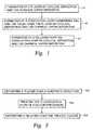
- FIG. 1is a flow chart illustrating one embodiment of a process of integrating a titanium layer and a titanium nitride layer by forming a titanium silicide layer and/or a titanium silicon nitride layer between the titanium layer and the titanium nitride layer.
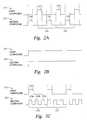
- FIG. 2Ais a graph of the control signals of an exemplary process for cyclical deposition of a material.
- FIG. 2Bis a graph of the control signals of one exemplary process for chemical vapor deposition of a material.
- FIG. 2Cis a graph of one exemplary process of the control signals for a combined mode of cyclical deposition and chemical vapor deposition.
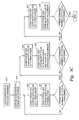
- FIG. 3Ais a flow chart illustrating one embodiment of a process utilizing a continuous flow of a purge gas to deposit a Ti layer, a TiSi x layer, and a TiN layer by cyclical deposition in the same chamber.
- FIG. 3Bis a flow chart illustrating one embodiment of a process utilizing pulses of a purge gas to deposit a Ti layer, a TiSi x layer, and a TiN layer by cyclical deposition in the same chamber.
- FIG. 3Cis a flow chart illustrating one embodiment of a process utilizing a continuous flow of a purge gas to deposit a Ti layer, a TiSi x N y layer, and a TiN layer by cyclical deposition in the same chamber.
- FIG. 3Dis a flow chart illustrating one embodiment of a process utilizing pulses of a purge gas to deposit a Ti layer, a TiSi x N y layer, and a TiN layer by cyclical deposition in the same chamber.
- FIGS. 4 and 4Aare drawings of an exemplary processing chamber that may be used to perform cyclical deposition, chemical vapor deposition, or a combined mode of cyclical deposition and chemical vapor deposition.
- FIG. 5is a flow chart illustrating another embodiment of a process of integrating a Ti layer and a TiN layer by soaking a Ti layer with a flow of a silicon precursor prior to deposition of a TiN layer thereover.
- FIG. 6is a schematic cross-sectional view of one embodiment of an exemplary application of an integrated Ti/TiN film stack.
- FIG. 7is a schematic cross-sectional view of another embodiment of an exemplary application of an integrated Ti/TiN film stack.
- FIG. 1is a flow chart illustrating one embodiment of a process of integrating a titanium (Ti) layer and a titanium nitride (TiN) layer by forming a titanium silicide (TiSi x ) layer and/or a titanium silicon nitride (TiSi x N y ) layer between the Ti layer and the TiN layer.
- a Ti layermay be formed over a substrate structure by cyclical deposition, chemical vapor deposition, or a combined mode of cyclical deposition and chemical vapor deposition.
- a passivation layercomprising titanium silicide and/or titanium silicon nitride may be formed over the Ti layer by cyclical deposition, chemical vapor deposition, or a combined mode of cyclical deposition and chemical vapor deposition.
- a TiN layermay be formed over the passivation layer by cyclical deposition, chemical vapor deposition, or a combined mode of cyclical deposition and chemical vapor deposition.
- the TiSi x layer or TiSi x N yhelps protect the interface between the Ti layer and a subsequently deposited TiN layer resulting in improved adhesion of the TiN layer thereover.
- the TiSi x layer or TiSi x N yreduces the attack of the halide from the titanium halide used during deposition of TiN and thus provides a Ti/TiN film stack with improved adhesion.
- substrate structureis intended to include any workpiece upon which film processing is performed and may be used to denote a substrate, such as a semiconductor substrate or a glass substrate, as well as other material layers formed on the substrate, such as a dielectric layer.
- cyclical depositionrefers to the sequential introduction of one or more compounds to deposit a thin layer over a structure and includes processing techniques such as atomic layer deposition.
- Compoundscan be reactants, reductants, precursors, catalysts, and mixtures thereof. Sequentially providing compounds may result in the adsorption of thin layers of the compounds over a substrate structure.
- the sequential introduction of compoundsmay be repeated to deposit a plurality of thin layers forming a conformal layer to a desired thickness.
- adsorptionand “adsorb” as used herein are defined to include chemisorption, physisorption, or any attractive and/or bonding forces which may be at work and/or which may contribute to the bonding, reaction, adherence, or occupation of a portion of a surface of a substrate structure.
- chemical vapor depositionrefers to deposition of materials in a primarily gas-phase and/or thermal co-reaction of compounds to form a layer and includes plasma enhanced and non-enhanced processes. A mode of deposition combining cyclical deposition and chemical vapor deposition may also be performed.
- FIG. 2Ais a graph of the control signals of an exemplary process for cyclical deposition of a material.
- One cycle 310comprises introducing a pulse 312 of a first compound 313 into a chamber by opening and closing a valve providing the first compound. After the pulse of the first compound, a pulse 314 of a second compound 315 is introduced into the chamber by opening and closing a valve providing the second compound. The cycle 310 may be repeated to deposit a desired thickness of the material.
- the pulses 312 of the first compound 313 and the pulses 314 of the second compound 315may be delivered with or without a carrier gas.
- pulses 312 of the first compound 313 and the pulses 314 of the second compound 315may be dosed into a continuous flow of a purge gas.
- purge gaseswhich may be used include, but are not limited to, helium (He), argon (Ar), nitrogen (N 2 ), hydrogen (H 2 ), and mixtures thereof.
- pulses 312 of the first compound 313 and pulses 314 of the second compound 315may be separated by pulses of a purge gas.
- pulses 312 of the first compound 313 and pulses 314 of a second compound 315may be separated by pump evacuation alone.
- cyclical depositioncomprises providing pulses of more than two compounds.
- FIG. 2Bis a graph of the control signals of one exemplary process for chemical vapor deposition of a material.
- Chemical vapor deposition of a materialmay comprise introducing a first compound 323 and a second compound 325 simultaneously to a chamber by opening a valve providing the first compound and by opening a valve providing the second compound.
- the first compound and the secondmay be delivered with or without a carrier gas.
- carrier gaseswhich may be used include, but are not limited to, helium (He), argon (Ar), nitrogen (N 2 ), hydrogen (H 2 ), and mixtures thereof.
- chemical vapor depositioncomprises providing more than two compounds.
- FIG. 2Cis a graph of one exemplary process of the control signals for a combined mode of cyclical deposition and chemical vapor deposition.
- One cycle 330comprises introducing at least one pulse 332 of a first compound 333 by opening and closing a valve providing the first compound and introducing pulses 334 of a second compound 335 by opening and closing a valve providing the second compound.
- One or more pulses 334 a of the second compound 335at least partially overlap with one or more pulses 332 of the first compound 333 in which the valve providing the first compound and the valve providing the second compound are both open at the same time for a period of time.
- One or more pulses 334 b , 334 c of the second compound 335do not overlap with one or more pulses 332 of the first compound 333 in which the valve providing the first compound is closed for a period of time while the valve providing the second compound is open.
- the cycle 330may be repeated to deposit a desired thickness of the material.
- the pulses 332 of the first compound 333 and the pulses 334 of the second compound 335may be delivered with or without a carrier gas.
- carrier gaseswhich may be used include, but are not limited to, helium (He), argon (Ar), nitrogen (N 2 ), hydrogen (H 2 ), and mixtures thereof.
- the pulses 332 of the first compound 333 and the pulses 334 of the second compound 335may be dosed into a continuous flow of a purge gas.
- purge gaseswhich may be used include, but are not limited to, helium (He), argon (Ar), nitrogen (N 2 ), hydrogen (H 2 ), and mixtures thereof.
- pulses 332 of the first compound 333 and pulses 334 of the second compound 335may be separated by pulses of a purge gas.
- pulses 332 of the first compound 333 and pulses 334 of a second compound 335may be separated by pump evacuation alone.
- a first compound and a second compoundare delivered at separate times to the substrate to provide a deposition process similar to cyclical deposition.
- a first compound and a second compoundare delivered at the same time to the substrate to provide a deposition process similar to chemical vapor deposition.
- a combined mode of cyclical depositioncomprises providing pulses of more than two compounds.
- one cyclemay comprise providing one pulse of a first compound and one pulse of a second compound in which the pulse of the first compound and the pulse of the second compound only partially overlap in time by opening a valve providing the first compound, then opening a valve providing the second compound, then closing the valve providing the first compound, and then closing the valve providing the second compound.
- FIGS. 2A and 2Cshow the duration of pulses of compounds provided over a relative length of time, show a specific order of pulses, and show a specific number of pulses per cycle. In other embodiments, other relative lengths of time, other order of the pulses, and other number of pulses are possible.
- deposition of Ticomprises utilizing a titanium precursor and a reductant.
- the titanium precursorpreferably comprises titanium tetrachloride (TiCl 4 ).
- titanium tetrachlorideTiCl 4
- examples of other titanium containing compoundsinclude, but are not limited to, titanium iodide (Til 4 ), titanium bromide (TiBr 4 ), other titanium halides, tetrakis(dimethylamino)titanium (TDMAT), tetrakis(diethylamino) titanium (TDEAT), other titanium organic compounds, and derivatives thereof.
- the reductantcomprises a hydrogen plasma.
- the hydrogen plasmais preferably provided by utilizing a hydrogen gas (H 2 ).
- a hydrogen gasH 2
- Other hydrogen containing gaseswhich may also be used include silane (SiH 4 ), borane (BH 3 ), diborane (B 2 H 6 ), triborane (B 3 H 9 ), among others.
- deposition of TiSi xcomprises utilizing a titanium precursor and a silicon precursor.
- the titanium precursorpreferably comprises TiCl 4 .
- Other titanium precursorsmay be used, such as the titanium precursors described above in regards to the deposition of Ti.
- the silicon precursorpreferably comprises silane (SiH 4 ).
- silicon containing compoundsinclude, but are not limited to disilane (Si 2 H 6 ), chlorosilane (SiH 3 Cl), dichlorosilane (SiH 2 Cl 2 ), trichlorosilane (SiHCl 3 ), silicon tetrachloride (SiCl 4 ), hexachlorodisilane (Si 2 Cl 6 ), and derivatives thereof.
- deposition of TiSi x N ycomprises utilizing a titanium precursor, a silicon precursor, and a nitrogen precursor.
- the titanium precursorpreferably comprises titanium tetrachloride (TiCl 4 ) and the silicon precursor preferably comprises silane (SiH 4 ).
- Other titanium precursors and silicon precursorsmay be used, such as the titanium precursors and silicon precursors described above in regards to the deposition of Ti and TiSi x .
- the nitrogen precursorpreferably comprises ammonia (NH 3 ).
- nitrogen precursorsexamples include, but are not limited to hydrazine (N 2 H 4 ), other N x H y compounds with x and y being integers, dimethyl hydrazine ((CH 3 ) 2 N 2 H 2 ), t-butylhydrazine (C 4 H 9 N 2 H 3 ), phenylhydrazine (C 6 H 5 N 2 H 3 ), 2,2′-azoisobutane ((CH 3 ) 6 C 2 N 2 ), ethylazide (C 2 H 5 N 3 ), and derivatives thereof.
- hydrazineN 2 H 4
- other N x H y compoundswith x and y being integers
- dimethyl hydrazine((CH 3 ) 2 N 2 H 2 )
- t-butylhydrazineC 4 H 9 N 2 H 3
- phenylhydrazineC 6 H 5 N 2 H 3
- 2,2′-azoisobutane(CH 3 ) 6 C
- deposition of TiNcomprises utilizing a titanium precursor and a nitrogen precursor.
- the titanium precursorpreferably comprises titanium tetrachloride (TiCl 4 ).
- Other titanium precursorsmay be used, such as the titanium precursors described above in regards to the deposition of Ti.
- the nitrogen precursorpreferably comprises a nitrogen plasma, NH 3 , or combinations thereof.
- nitrogen precursorsexamples include, but are not limited to hydrazine (N 2 H 4 ), other N x H y compounds with x and y being integers, dimethyl hydrazine ((CH 3 ) 2 N 2 H 2 ), t-butylhydrazine (C 4 H 9 N 2 H 3 ), phenylhydrazine (C 6 H 5 N 2 H 3 ), 2,2′-azoisobutane ((CH 3 ) 6 C 2 N 2 ), ethylazide (C 2 H 5 N 3 ), and derivatives thereof.
- hydrazineN 2 H 4
- other N x H y compoundswith x and y being integers
- dimethyl hydrazine((CH 3 ) 2 N 2 H 2 )
- t-butylhydrazineC 4 H 9 N 2 H 3
- phenylhydrazineC 6 H 5 N 2 H 3
- 2,2′-azoisobutane(CH 3 ) 6 C
- nitrogen containing gaseswhich may also be used to generate a nitrogen plasma include, but are not limited to, NH 3 , N x H y with x and y being integers (e.g., hydrazine (N 2 H 4 )), a mixture of hydrogen gas (H 2 ) and nitrogen gas (N 2 ), mixtures thereof, other gases or gas mixtures containing hydrogen and nitrogen.
- step 10 , step 20 , and step 30are performed in separate chambers. In another embodiment, two or more of the steps 10 , 20 , 30 are performed in the same chamber. In still another embodiment, all of the steps 10 , 20 , 30 are performed in the same chamber.
- FIG. 3Ais a flow chart illustrating one embodiment of a process utilizing a continuous flow of a purge gas to deposit a Ti layer, a TiSi x layer, and a TiN layer by cyclical deposition in the same chamber.
- a substrateis provided to the process chamber.
- the process chamber conditionssuch as for example the substrate temperature and pressure, may be adjusted.
- a purge gas streamis established within the process chamber.
- a pulse of a Ti precursorsuch as TiCl 4 , is added or dosed into the purge gas stream.
- step 608after the pulse of the Ti precursor a pulse of a reductant, such as a hydrogen plasma, is dosed into the purge gas stream. Step 606 and step 608 are repeated until a predetermined number of cycles are performed to form a Ti layer.
- a pulse of a reductantsuch as a hydrogen plasma
- step 606 and step 608are repeated until a predetermined number of cycles are performed to form a Ti layer.
- another pulse of the Ti precursoris dosed into the purge gas stream.
- step 612after the pulse of the Ti precursor, a pulse of a Si precursor, such as a SiH 4 , is dosed into the purge gas stream. Step 610 and step 612 are repeated until a predetermined number of cycles are performed to form a TiSi x layer.
- step 614after a predetermined number of cycles of step 610 and step 612 are performed, another pulse of the Ti precursor is dosed into the purge gas stream.
- step 616after the pulse of the Ti precursor, a pulse of a nitrogen precursor, such as NH 3 or a nitrogen plasma, is dosed into the purge gas stream. Step 614 and step 616 are repeated until a predetermined number of cycles are performed to form a TiN layer.
- FIG. 3Bis a flow chart illustrating one embodiment of a process utilizing pulses of a purge gas to deposit a Ti layer, a TiSi x layer, and a TiN layer by cyclical deposition in the same chamber.
- a substrateis provided to a process chamber.
- the process chamber conditionssuch as for example the substrate temperature and pressure, may be adjusted.
- a pulse of a purge gasis provided to the process chamber.
- a pulse of a Ti precursorsuch as TiCl 4
- step 628after the pulse of the Ti precursor, another pulse of the purge gas is provided.
- step 630after the pulse of the purge gas, a pulse of a reductant, such as a hydrogen plasma, is provided. Steps 624 , 626 , 628 , and 630 are repeated until a predetermined number of cycles are performed to form a Ti layer. Referring to step 632 , after a predetermined number of cycles of steps 624 , 626 , 628 , and 630 are performed, another pulse of the purge gas is provided to the process chamber. Referring to step 634 , after the pulse of the purge gas, another pulse of the Ti precursor is provided to the process chamber. In step 636 , after the pulse of the Ti precursor, another pulse of the purge gas is provided.
- a pulse of a reductantsuch as a hydrogen plasma
- step 638after the pulse of the purge gas, a pulse of a silicon precursor, such as silane (SiH 4 ), is provided. Steps 632 , 634 , 636 , and 638 are repeated until a predetermined number of cycles are performed to form a TiSi x , layer.
- a pulse of the purge gasis provided to the process chamber.
- step 642after the pulse of the purge gas, another pulse of the Ti precursor is provided to the process chamber.
- step 644after the pulse of the Ti precursor, another pulse of the purge gas is provided.
- step 646after the pulse of the purge gas, a pulse of a pulse of a nitrogen precursor, such as NH 3 or a nitrogen plasma, is provided. Steps 640 , 642 , 644 , and 646 are repeated until a predetermined number of cycles are performed to form a TiN layer.
- a pulse of a pulse of a nitrogen precursorsuch as NH 3 or a nitrogen plasma
- FIG. 3Cis a flow chart illustrating one embodiment of a process utilizing a continuous flow of a purge gas to deposit a Ti layer, a TiSi x N y layer, and a TiN layer by cyclical deposition in the same chamber.
- a substrateis provided to the process chamber.
- the process chamber conditionssuch as for example the substrate temperature and pressure, may be adjusted.
- a purge gas streamis established within the process chamber.
- a pulse of a Ti precursorsuch as TiCl 4 , is added or dosed into the purge gas stream.
- step 658after the pulse of the Ti precursor a pulse of a reductant, such as a hydrogen plasma, is dosed into the purge gas stream.
- Step 656 and step 658are repeated until a predetermined number of cycles are performed to form a Ti layer.
- step 660after a predetermined number of cycles of step 656 and step 658 are performed, another pulse of the Ti precursor is dosed into the purge gas stream.
- step 662after the pulse of the Ti precursor, a pulse of a Si precursor, such as SiH 4 , and a pulse of a nitrogen precursor, such as NH 3 , is dosed into the purge gas stream.
- the pulses of the Si precursor and the nitrogen precursormay be introduced separately or may be introduced in which the pulses at least partially overlap in time.
- Step 660 and step 662are repeated until a predetermined number of cycles are performed to form a TiSi x N y layer.
- step 664after a predetermined number of cycles of step 660 and step 662 are performed, another pulse of the Ti precursor is dosed into the purge gas stream.
- step 666after the pulse of the Ti precursor, another pulse of the nitrogen precursor is dosed into the purge gas stream.
- Step 664 and step 666are repeated until a predetermined number of cycles are performed to form a TiN layer.
- FIG. 3Dis a flow chart illustrating one embodiment of a process utilizing pulses of a purge gas to deposit a Ti layer, a TiSi x N y layer, and a TiN layer by cyclical deposition in the same chamber.
- a substrateis provided to a process chamber.
- the process chamber conditionssuch as for example the substrate temperature and pressure, may be adjusted.
- a pulse of a purge gasis provided to the process chamber.
- a pulse of a Ti precursorsuch as TiCl 4
- step 678after the pulse of the Ti precursor, another pulse of the purge gas is provided.
- step 680after the pulse of the purge gas, a pulse of a reductant, such as a hydrogen plasma, is provided. Steps 674 , 676 , 678 , and 680 are repeated until a predetermined number of cycles are performed to form a Ti layer. Referring to step 682 , after a predetermined number of cycles of steps 674 , 676 , 678 , and 680 are performed, another pulse of the purge gas is provided to the process chamber. Referring to step 684 , after the pulse of the purge gas, another pulse of the Ti precursor is provided to the process chamber. In step 686 , after the pulse of the Ti precursor, another pulse of the purge gas is provided.
- a pulse of a reductantsuch as a hydrogen plasma
- step 688after the pulse of the purge gas, a pulse of a silicon precursor, such as silane (SiH 4 ), and a pulse of a nitrogen precursor, such as ammonia (NH 3 ), is provided.
- the pulses of the Si precursor and the nitrogen precursormay be introduced separately or may be introduced in which the pulses at least partially overlap in time.
- Steps 682 , 684 , 686 , and 688are repeated until a predetermined number of cycles are performed to form a TiSi x N y layer.
- step 690after a predetermined number of cycles of steps 682 , 684 , 686 , and 688 are performed, another pulse of the purge gas is provided to the process chamber.
- step 692after the pulse of the purge gas, another pulse of the Ti precursor is provided to the process chamber.
- step 694after the pulse of the Ti precursor, another pulse of the purge gas is provided.
- step 696after the pulse of the purge gas, another pulse of a pulse of a nitrogen precursor is provided. Steps 690 , 692 , 694 , and 696 are repeated until a predetermined number of cycles are performed to form a TiN layer.
- the same Ti precursoris preferably used to deposit a Ti layer, a TiSi x /TiSi x N y layer, and a TiN layer.
- TiCl 4may be used to deposit a Ti layer, a TiSi x /TiSi x N y layer, and a TiN layer.
- FIGS. 3 A- 3 Dshow the deposition of a Ti layer, a TiSi x /TiSi x N y layer, and a TiN layer in a single chamber.
- deposition of a Ti layer, a TiSi x /TiSi x N y layer, and a TiN layermay be performed in more than one chamber.
- two or more chambersmay be used to deposit a Ti layer, a TiSi x /TiSi x N y layer, and a TiN layer.
- FIGS. 3 A- 3 Dshow deposition of a Ti layer, a TiSi x /TiSi x N y layer, and a TiN layer by cyclical deposition.
- each layermay be deposited by the same or different deposition technique selected from the group including cyclical deposition, chemical vapor deposition, and a combined mode of cyclical deposition and chemical vapor deposition.
- FIGS. 4 and 4Aare drawings of an exemplary processing chamber 100 that may be used to perform cyclical deposition, chemical vapor deposition, or a combined mode of cyclical deposition and chemical vapor deposition. Other chambers may also be used.
- the chamber 100comprises a chamber body 102 including a substrate support 112 having a substrate receiving surface 111 to support a substrate 110 .
- the chambermay be adapted to heat the substrate 110 , such as by a heated substrate support or by using heat lamps.
- a gas distribution system 130is disposed at an upper portion of the chamber body 102 to provide a gas to the chamber 100 .
- the gas distribution system 130comprises a gas box 132 , a top shower plate 160 positioned below the gas box 132 , and a bottom shower plate 170 positioned below the top shower plate 160 .
- FIG. 4Ais a schematic partial cross-sectional view of a portion of the gas box 132 , a portion of the top shower plate 160 , and a portion of the bottom shower plate 170 of FIG. 4.
- the gas box 132comprises a central gas channel 137 and a plurality of outer gas channels 143 .
- the central gas channel 137provides one discrete path for the flow of one or more gases through the gas box 132 while the outer channels 143 provides another discrete path for the flow of one or more gases through the gas box 132 .
- the central gas channel 137is coupled to a first gas source 135 (FIG. 4) through valve 136 (FIG. 4).
- the central gas channel 137has a first gas outlet 138 and is adapted to deliver a first gas from the first gas source 135 to a gas conduit 210 .
- gasas used herein is intended to mean a single gas or a gas mixture.
- the outer gas channels 143are coupled to a second gas source 141 (FIG. 4) through valve 142 (FIG. 4).
- the outer gas channels 143have second gas outlets 144 and are adapted to deliver a second gas from the second gas source 141 to the top shower plate 160 .
- the second gas outlets 144 of the outer gas channels 143are adapted to deliver the second gas proximate a central portion of the top shower plate.
- Gas sources 135 , 141may be adapted to store a gas or liquid precursor in a cooled, heated, or ambient environment.
- the valves 136 , 142control delivery of the first gas and the second gas into the central gas channel 137 and the outer gas channels 143 respectively and may be electrically controlled valves, pneumatically controlled valves, piezoelectric valves, or other suitable valves.
- a third gas sourcemay be coupled to the outer gas channels 143 to provided a third gas to the top shower plate 160 or may be coupled to the central gas channel 137 to provided a third gas to the gas conduit 210 .
- the top shower plate 160has a plurality of holes 162 to accommodate a gas flow therethrough from the outer gas channels 143 of the gas box 132 to the bottom shower plate 170 .
- the top shower plate 160is separated from the bottom shower plate 170 by an insulator 164 to electrically insulate the top shower plate 160 from the bottom shower plate 170 .
- the bottom shower plate 170may be disposed on an upper portion of the chamber body 102 , such as on a lid rim 166 disposed on the chamber body 102 .
- the lid rim 166comprises an insulating material to electrically insulate the bottom shower plate 170 from the chamber body 102 .
- the gas conduit 210is disposed through an aperture 163 in the top shower plate 160 and is disposed on the bottom shower plate 170 .
- the gas conduit 210is made of an insulating material to prevent electrical coupling of the top shower plate 160 and the bottom shower plate 170 .
- the bottom shower plate 170comprises a first piece 172 connected to a second piece 180 .
- the first piece 172has a plurality of holes 174 to provide a flow of a gas therethrough.
- the second piece 180comprises a plurality of columns 182 having column holes 183 formed therethrough and a plurality of grooves 184 having groove holes 185 formed therethrough.
- the top surface of the columns 182are connected to the bottom surface of the first piece 172 so that the column holes 183 align with the holes 174 of the first piece 172 . Therefore, one discrete passageway is provided through the holes of the first piece 172 and through the column holes 183 of the columns 182 to deliver a gas flow from the top shower plate 160 to the substrate receiving surface 111 .
- the aperture 175is formed through the first piece 172 and aligns with the grooves on the second piece 180 . Therefore, another discrete passageway is provided through the aperture 175 of the first piece 172 and through the grooves 184 and groove holes 185 of the second piece 180 to deliver a gas flow from the gas conduit 210 to the substrate receiving surface 111 .
- a power source 190may be coupled to the top shower plate 160 through the gas box 132 to provide a power electrode and the bottom shower plate 170 may be grounded to provide a ground electrode.
- the power source 190may be an RF or DC power source. An electric field may be established between the top shower plate 160 and the bottom shower plate 170 to generate a plasma from the gases introduced between the top shower plate 160 and the bottom shower plate 170 .
- the power source 190may be coupled to a matching network 194 to control delivery of power to the power source 190 .
- the power source 190may selectively provide power to selectively perform plasma and non-plasma processes.
- the bottom shower plate 170may be optionally coupled to a power source 192 in addition to the power source 190 coupled to the top shower plate 160 and may be selectively powered or grounded.
- the power sources 190 and 192are coupled to the matching network 194 to control delivery of any amount of power to the power source 190 and to control delivery of any amount of power to the power source 192 .
- the matching network 194may control the delivery of power to the power sources 190 , 192 so that the top shower plate 160 and the bottom shower plate 170 are at the same or substantially the same potential.
- the top shower plate 160 and the bottom shower plate 170act as one electrode and the substrate support 112 acts as another electrode of spaced apart electrodes in which an electric field is established between the bottom shower plate 170 and the substrate support 112 to generate a plasma from the gases introduced between the bottom shower plate 170 and the substrate support 112 . Therefore, power may be selectively provided to power sources 190 , 192 to selectively generate a plasma between the top shower plate 160 and the bottom shower plate 170 or between the bottom shower plate 170 and the substrate support 112 . Thus, the power sources 190 , 192 may selectively provide power to selectively perform plasma and non-plasma processes.
- a vacuum system 196is in communication with a pumping channel 197 formed in the chamber body 102 to evacuate gases from the chamber 100 and to help maintain a desired pressure or a desired pressure range inside the chamber 100 .
- Control unit 176may be coupled to the chamber 100 to control processing conditions.
- FIG. 5is a flow chart illustrating another embodiment of a process of integrating a Ti layer and a TiN layer by soaking a Ti layer with a flow of a silicon precursor prior to deposition of a TiN layer thereover.
- a Ti layeris deposited over a substrate structure.
- the Ti layermay be deposited by methods including, but are not limited to, chemical vapor deposition, cyclical deposition, physical vapor deposition, and combinations thereof.
- the Ti layermay be deposited by chemical vapor deposition or cyclical deposition by utilizing a titanium precursor, such as titanium tetrachloride (TiCl 4 ), and a reducing agent, such as a hydrogen plasma.
- TiCl 4titanium tetrachloride
- titanium containing compoundsexamples include, but are not limited to, titanium iodide (Til 4 ), titanium bromide (TiBr 4 ), other titanium halides, tetrakis(dimethylamino)titanium (TDMAT), tetrakis(diethylamino) titanium (TDEAT), other titanium organic compounds, and derivatives thereof.
- the hydrogen plasmais preferably provided by utilizing a hydrogen gas (H 2 ).
- Other hydrogen containing gaseswhich may also be used include silane (SiH 4 ), borane (BH 3 ), diborane (B 2 H 6 ), triborane (B 3 H 9 ), among others.
- the Ti layeris treated with a soak with a silicon precursor by flowing in the silicon precursor into a process chamber.
- the silicon precursoris preferably silane (SiH 4 ).
- Other silicon precursorsmay also be used, such as disilane (Si 2 H 6 ), and less preferably, dichlorosilane, or silicon tetrachloride.
- the silicon precursormay be flowed in with a carrier gas, such as a helium gas (He), an argon gas (Ar), hydrogen gas (H 2 ), nitrogen gas (N 2 ), other suitable gases, and combinations thereof.
- the substrateis preferably maintained at a substrate temperature of about 550° C. or less, preferably about 500° C.
- TiSi xtitanium suicide
- the TiSi xhelps protect the interface between the Ti layer and a subsequently deposited TiN layer resulting in improved adhesion of the TiN layer thereover.
- a soak with a silicon precursor performed at a heater temperature of about 550° C. or lessreduces the formation of polysilicon or amorphous silicon which would be undesirable due to the higher resistance of polysilicon or amporphous silicon in comparison to TiSi x .
- a TiN layeris deposited over the treated Ti layer.
- the TiN layermay be deposited by such methods, with include, but are not limited to, chemical vapor deposition, cyclical deposition, physical vapor deposition, and combinations thereof.
- the TiN layermay be deposited by chemical vapor deposition or cyclical deposition by utilizing a titanium precursor, such as titanium tetrachloride (TiCl 4 ), and a nitrogen precursor, such as ammonia (NH 3 ) or a nitrogen plasma.
- TiCl 4titanium tetrachloride
- NH 3ammonia
- the TiSi x formed during the soak with a silicon precursorprotects the Ti layer from etching or attack from the halogen in the titanium halide, such as chlorine from TiCl 4 , used during chemical vapor deposition or cyclical deposition of the TiN layer.
- Examples of other nitrogen precursors which may be used to form the TiN layerinclude, but are not limited to hydrazine (N 2 H 4 ), other N x H y compounds with x and y being integers, dimethyl hydrazine ((CH 3 ) 2 N 2 H 2 ), t-butylhydrazine (C 4 H 9 N 2 H 3 ), phenylhydrazine (C 6 H 5 N 2 H 3 ), 2,2′-azoisobutane ((CH 3 ) 6 C 2 N 2 ), ethylazide (C 2 H 5 N 3 ), and derivatives thereof.
- hydrazineN 2 H 4
- other N x H y compounds with x and y being integersdimethyl hydrazine ((CH 3 ) 2 N 2 H 2 ), t-butylhydrazine (C 4 H 9 N 2 H 3 ), phenylhydrazine (C 6 H 5 N 2 H 3 ), 2,2′-azoiso
- nitrogen containing gaseswhich may also be used to generate a nitrogen plasma to form the TiN layer include, but are not limited to, NH 3 , N x H y with x and y being integers (e.g., hydrazine (N 2 H 4 )), a mixture of hydrogen gas (H 2 ) and nitrogen gas (N 2 ), mixtures thereof, other gases or gas mixtures containing hydrogen and nitrogen.
- step 502 , step 504 , and step 506may each be performed in separate chambers.
- two or more of step 502 , step 504 , and step 506may be performed in the same chamber.
- deposition of a Ti layer and a soak of the Ti layer with a silicon precursormay be performed in the same chamber.
- a soak of a Ti layer with a silicon precursor and deposition of a TiN layermay be performed in the same chamber.
- deposition of a Ti layer, a soak of the Ti layer with a silicon precursor, and deposition of a TiN over the treated Ti layermay be performed in the same chamber.
- two or more of step 502 , step 504 , and step 506are performed in the same chamber to increase throughput of processing the substrates.
- Processing chamberswhich may be used to deposit a Ti layer, perform a soak with a silicon precursor, and/or deposit a TiN layer include the chamber as described in reference to FIGS. 4 and 4A.
- Other chambersmay also be used such as the processing chamber described in U.S. patent application (Ser. No. 10/032,293) entitled “Chamber Hardware Design For Titanium Nitride Atomic Layer Deposition,” filed on Dec. 21, 2001; the processing chamber described in U.S. patent application (Ser. No. 10/016,300) entitled “Lid Assembly For A Processing System To Facilitate Sequential Deposition Techniques,” filed on Dec. 12, 2001, which claims priority to U.S. Provisional Application Serial No. 60/305,970 filed on Jul.
- One exemplary process of treating a Ti layer with a soak of a silicon precursorcomprises flowing in silane (SiH 4 ) into a chamber, such as chamber 100 described in reference to FIG. 4, at a flow rate between about 5 sccm and about 500 sccm, preferably about 100 sccm.
- Silanemay be introduced with a carrier gas, such as a helium gas (He), an argon gas (Ar), hydrogen gas (H 2 ), nitrogen gas (N 2 ), other suitable gases, and combinations thereof.
- the chambermay be maintained at a pressure between about 0.1 torr to about 50 torr, preferably about 3 torr.
- the substrateis preferably maintained at a substrate temperature about 550° C.
- the SiH 4 soakis preferably carried out for a time period between about 5 seconds and about 60 seconds. In general, treatment time will depend on the flow rate of SiH 4 and the pressure of the chamber.
- FIG. 6is a schematic cross-sectional view of one embodiment of an exemplary application of an integrated Ti/TiN film stack formed by the process of FIG. 1 or FIG. 5.
- a doped source/drain region 854may be formed over a substrate 852 .
- the substrate 852may be a semiconductor substrate, such as a silicon substrate.
- a dielectric layer 858such as a silicon dioxide layer or a low-k dielectric layer, may be formed over the substrate 852 .
- a low-k dielectric layeris an oxidized organosilane layer or an oxidized organosiloxane layer described in more detail in U.S. Pat. No. 6,348,725, issued Feb.
- the dielectric layer 858may be patterned and etched to form an aperture.
- a titanium layer 859may be deposited over the aperture to form titanium silicide 856 in situ or in an annealing step.
- a passivation layer 860comprising TiSi x , TiSi x N y , or combinations thereof is deposited over the titanium layer 859 or formed by a soak of the titanium layer 859 with a silicon precursor.
- a TiN layer 861is deposited over the passivation layer 860 .
- a conductive layer 862comprising a conductive material, such as tungsten, copper, aluminum, and combinations thereof, may be deposited over the TiN layer 861 .
- FIG. 7is a schematic cross-sectional view of another embodiment of an exemplary application of an integrated Ti/TiN film stack formed by the process of FIG. 1 or FIG. 5.
- the film stack 1200includes an underlying substrate 1202 , such as a semiconductor substrate, and includes a doped source/drain region 1204 .
- a metal silicide layer 1206such as a titanium silicide layer, nickel silicide layer, cobalt silicide layer, or tungsten silicide layer, may be formed over the region 1204 .
- a dielectric layer 1208such as a silicon dioxide layer or a low-k dielectric layer, may be formed over the metal silicide layer 1206 .
- a low-k dielectric layeris an oxidized organosilane layer or an oxidized organosiloxane layer described in more detail in U.S. Pat. No. 6,348,725, issued Feb. 19, 2002, which is incorporated by reference herein.
- the dielectric layer 1208may be patterned and etched to form an aperture exposing the metal silicide layer 1206 .
- a titanium layer 1212may be formed over the aperture.
- a passivation layer 1214comprising TiSi x , TiSi x N y , or combinations thereof is deposited over the titanium layer 1212 or formed by a soak of the titanium layer 1212 with a silicon precursor.
- a titanium nitride layer 1216may be formed over the passivation layer 1214 .
- a conductive layer 1222comprising a conductive material, such as tungsten, copper, aluminum, and combinations thereof, may be deposited over the titanium nitride layer 1216 .
- Other applications of the integrated Ti/TiN film stack
Landscapes
- Chemical & Material Sciences (AREA)
- Engineering & Computer Science (AREA)
- General Chemical & Material Sciences (AREA)
- Chemical Kinetics & Catalysis (AREA)
- Physics & Mathematics (AREA)
- Organic Chemistry (AREA)
- Metallurgy (AREA)
- Mechanical Engineering (AREA)
- Materials Engineering (AREA)
- Computer Hardware Design (AREA)
- Power Engineering (AREA)
- Microelectronics & Electronic Packaging (AREA)
- Manufacturing & Machinery (AREA)
- General Physics & Mathematics (AREA)
- Condensed Matter Physics & Semiconductors (AREA)
- Plasma & Fusion (AREA)
- Analytical Chemistry (AREA)
- Inorganic Chemistry (AREA)
- Electromagnetism (AREA)
- Electrodes Of Semiconductors (AREA)
- Chemical Vapour Deposition (AREA)
- Formation Of Insulating Films (AREA)
Abstract
Description
- This application claims benefit of U.S. provisional patent application serial No. 60/352,191, filed Jan. 26, 2002, which is herein incorporated by reference.[0001]
- 1. Field of the Invention[0002]
- Embodiments of the present invention generally relate to an apparatus and method of integration of titanium and titanium nitride layers.[0003]
- 2. Description of the Related Art[0004]
- Reliably producing sub-micron and smaller features is one of the key technologies for the next generation of very large scale integration (VLSI) and ultra large scale integration (ULSI) of semiconductor devices. However, as the fringes of circuit technology are pressed, the shrinking dimensions of interconnects in VLSI and ULSI technology have placed additional demands on the processing capabilities. The multilevel interconnects that lie at the heart of this technology require precise processing of high aspect ratio features, such as vias and other interconnects. Reliable formation of these interconnects is very important to VLSI and ULSI success and to the continued effort to increase circuit density and quality of individual substrates.[0005]
- As circuit densities increase, the widths of interconnects, such as vias, trenches, contacts, and other features, as well as the dielectric materials between them, decrease to sub-micron dimensions (e.g., 0.20 micrometers or less), whereas the thickness of the dielectric layers remains substantially constant, with the result that the aspect ratios for the features, i.e., their height divided by width, increase. Many traditional deposition processes have difficulty filling sub-micron structures where the aspect ratio exceeds 4:1. Therefore, there is a great amount of ongoing effort being directed at the formation of substantially void-free and seam-free sub-micron features having high aspect ratios.[0006]
- In the manufacture of integrated circuits, a titanium/titanium (Ti/TiN) film stack, a titanium nitride layer over a titanium layer, is often used as a liner barrier. For example, Ti/TiN film stack may be used to provide contacts to the source and drain of a transistor. For example, a Ti layer is deposited over a silicon substrate. A portion of the Ti layer, which is in contact with the silicon substrate, is converted to titanium silicide (TiSi[0007]x) in situ or in an annealing step. A TiN layer is deposited over the Ti layer. The titanium nitride layer is used as a barrier layer to inhibit the diffusion of metals into regions underlying the barrier layer. A metal layer, such as a tungsten (W) layer, is deposited over the TiN layer.
- A Ti layer and a TiN layer may be formed by chemical vapor deposition and/or physical vapor deposition techniques. One example of forming a Ti Layer by chemical vapor deposition includes reacting titanium tetrachloride (TiCl[0008]4) with a hydrogen plasma. One example of forming a TiN layer by chemical vapor deposition includes reacting TiCl4with a nitrogen reactant, such as a nitrogen plasma or ammonia (NH3). One problem with the use of TiCl4-based chemistry used to form a TiN layer over a Ti layer is that reliability problems can occur. In particular, the TiN layer may have poor adhesion over the Ti layer, resulting in peeling of the TiN layer off the Ti layer.
- Therefore, there is a need for an improved apparatus and method of integration of titanium and titanium nitride layers.[0009]
- Embodiments of the present invention generally relate to an apparatus and method of integration of titanium and titanium nitride layers. One embodiment includes providing one or more cycles of a first set of compounds, providing one or more cycles of a second set of compounds, and providing one or more cycles of a third set of compounds. One cycle of the first set of compounds includes introducing a titanium precursor and a reductant. One cycle of the second set of compounds includes introducing the titanium precursor and a silicon precursor. One cycle of the third set of compounds includes introducing the titanium precursor and a nitrogen precursor. Another embodiment includes depositing a titanium layer utilizing titanium halide. Then, a passivation layer is deposited over the titanium layer utilizing titanium halide. The passivation layer may comprise titanium silicide, titanium silicon nitride, and combinations thereof. Then, a titanium nitride layer is deposited over the passivation layer utilizing titanium halide. Still another embodiment comprises depositing a titanium layer over a surface of a substrate. Then, the titanium layer is treated with a soak with a silicon precursor at a substrate temperature of about 550° C. or less to form a treated titanium layer. Then, a titanium nitride layer is deposited over the treated titanium layer.[0010]
- So that the manner in which the above recited features of the present invention are attained and can be understood in detail, a more particular description of the invention, briefly summarized above, may be had by reference to the embodiments thereof which are illustrated in the appended drawings. It is to be noted, however, that the appended drawings illustrate only typical embodiments of this invention and are therefore not to be considered limiting of its scope, for the invention may admit to other equally effective embodiments.[0011]
- FIG. 1 is a flow chart illustrating one embodiment of a process of integrating a titanium layer and a titanium nitride layer by forming a titanium silicide layer and/or a titanium silicon nitride layer between the titanium layer and the titanium nitride layer.[0012]
- FIG. 2A is a graph of the control signals of an exemplary process for cyclical deposition of a material.[0013]
- FIG. 2B is a graph of the control signals of one exemplary process for chemical vapor deposition of a material.[0014]
- FIG. 2C is a graph of one exemplary process of the control signals for a combined mode of cyclical deposition and chemical vapor deposition.[0015]
- FIG. 3A is a flow chart illustrating one embodiment of a process utilizing a continuous flow of a purge gas to deposit a Ti layer, a TiSi[0016]xlayer, and a TiN layer by cyclical deposition in the same chamber.
- FIG. 3B is a flow chart illustrating one embodiment of a process utilizing pulses of a purge gas to deposit a Ti layer, a TiSi[0017]xlayer, and a TiN layer by cyclical deposition in the same chamber.
- FIG. 3C is a flow chart illustrating one embodiment of a process utilizing a continuous flow of a purge gas to deposit a Ti layer, a TiSi[0018]xNylayer, and a TiN layer by cyclical deposition in the same chamber.
- FIG. 3D is a flow chart illustrating one embodiment of a process utilizing pulses of a purge gas to deposit a Ti layer, a TiSi[0019]xNylayer, and a TiN layer by cyclical deposition in the same chamber.
- FIGS. 4 and 4A are drawings of an exemplary processing chamber that may be used to perform cyclical deposition, chemical vapor deposition, or a combined mode of cyclical deposition and chemical vapor deposition.[0020]
- FIG. 5 is a flow chart illustrating another embodiment of a process of integrating a Ti layer and a TiN layer by soaking a Ti layer with a flow of a silicon precursor prior to deposition of a TiN layer thereover.[0021]
- FIG. 6 is a schematic cross-sectional view of one embodiment of an exemplary application of an integrated Ti/TiN film stack.[0022]
- FIG. 7 is a schematic cross-sectional view of another embodiment of an exemplary application of an integrated Ti/TiN film stack.[0023]
- Formation of a TiSi[0024]xand/or a TiSixNyFilm
- FIG. 1 is a flow chart illustrating one embodiment of a process of integrating a titanium (Ti) layer and a titanium nitride (TiN) layer by forming a titanium silicide (TiSi[0025]x) layer and/or a titanium silicon nitride (TiSixNy) layer between the Ti layer and the TiN layer. In
step 10, a Ti layer may be formed over a substrate structure by cyclical deposition, chemical vapor deposition, or a combined mode of cyclical deposition and chemical vapor deposition. Instep 20, a passivation layer comprising titanium silicide and/or titanium silicon nitride may be formed over the Ti layer by cyclical deposition, chemical vapor deposition, or a combined mode of cyclical deposition and chemical vapor deposition. Instep 30, a TiN layer may be formed over the passivation layer by cyclical deposition, chemical vapor deposition, or a combined mode of cyclical deposition and chemical vapor deposition. - Not wishing to be bound by theory, it is believed that the TiSi[0026]xlayer or TiSixNyhelps protect the interface between the Ti layer and a subsequently deposited TiN layer resulting in improved adhesion of the TiN layer thereover. In the embodiment in which TiN is deposited utilizing a titanium halide, it is believed that the TiSixlayer or TiSixNyreduces the attack of the halide from the titanium halide used during deposition of TiN and thus provides a Ti/TiN film stack with improved adhesion.
- The term “substrate structure” as used herein is intended to include any workpiece upon which film processing is performed and may be used to denote a substrate, such as a semiconductor substrate or a glass substrate, as well as other material layers formed on the substrate, such as a dielectric layer. The term “cyclical deposition” as used herein refers to the sequential introduction of one or more compounds to deposit a thin layer over a structure and includes processing techniques such as atomic layer deposition. Compounds can be reactants, reductants, precursors, catalysts, and mixtures thereof. Sequentially providing compounds may result in the adsorption of thin layers of the compounds over a substrate structure. The sequential introduction of compounds may be repeated to deposit a plurality of thin layers forming a conformal layer to a desired thickness. The terms “adsorption” and “adsorb” as used herein are defined to include chemisorption, physisorption, or any attractive and/or bonding forces which may be at work and/or which may contribute to the bonding, reaction, adherence, or occupation of a portion of a surface of a substrate structure. The term “chemical vapor deposition” as used herein refers to deposition of materials in a primarily gas-phase and/or thermal co-reaction of compounds to form a layer and includes plasma enhanced and non-enhanced processes. A mode of deposition combining cyclical deposition and chemical vapor deposition may also be performed.[0027]
- FIG. 2A is a graph of the control signals of an exemplary process for cyclical deposition of a material. One[0028]
cycle 310 comprises introducing apulse 312 of afirst compound 313 into a chamber by opening and closing a valve providing the first compound. After the pulse of the first compound, apulse 314 of asecond compound 315 is introduced into the chamber by opening and closing a valve providing the second compound. Thecycle 310 may be repeated to deposit a desired thickness of the material. Thepulses 312 of thefirst compound 313 and thepulses 314 of thesecond compound 315 may be delivered with or without a carrier gas. Examples of carrier gases which may be used include, but are not limited to, helium (He), argon (Ar), nitrogen (N2), hydrogen (H2), and mixtures thereof. In one embodiment, thepulses 312 of thefirst compound 313 and thepulses 314 of thesecond compound 315 may be dosed into a continuous flow of a purge gas. Examples of purge gases which may be used include, but are not limited to, helium (He), argon (Ar), nitrogen (N2), hydrogen (H2), and mixtures thereof. In other embodiments,pulses 312 of thefirst compound 313 andpulses 314 of thesecond compound 315 may be separated by pulses of a purge gas. In still other embodiments,pulses 312 of thefirst compound 313 andpulses 314 of asecond compound 315 may be separated by pump evacuation alone. In other embodiments, cyclical deposition comprises providing pulses of more than two compounds. - FIG. 2B is a graph of the control signals of one exemplary process for chemical vapor deposition of a material. Chemical vapor deposition of a material may comprise introducing a[0029]
first compound 323 and asecond compound 325 simultaneously to a chamber by opening a valve providing the first compound and by opening a valve providing the second compound. The first compound and the second may be delivered with or without a carrier gas. Examples of carrier gases which may be used include, but are not limited to, helium (He), argon (Ar), nitrogen (N2), hydrogen (H2), and mixtures thereof. In other embodiments, chemical vapor deposition comprises providing more than two compounds. - FIG. 2C is a graph of one exemplary process of the control signals for a combined mode of cyclical deposition and chemical vapor deposition. One[0030]
cycle 330 comprises introducing at least onepulse 332 of afirst compound 333 by opening and closing a valve providing the first compound and introducing pulses334 of asecond compound 335 by opening and closing a valve providing the second compound. One ormore pulses 334aof thesecond compound 335 at least partially overlap with one ormore pulses 332 of thefirst compound 333 in which the valve providing the first compound and the valve providing the second compound are both open at the same time for a period of time. One ormore pulses second compound 335 do not overlap with one ormore pulses 332 of thefirst compound 333 in which the valve providing the first compound is closed for a period of time while the valve providing the second compound is open. Thecycle 330 may be repeated to deposit a desired thickness of the material. Thepulses 332 of thefirst compound 333 and the pulses334 of thesecond compound 335 may be delivered with or without a carrier gas. Examples of carrier gases which may be used include, but are not limited to, helium (He), argon (Ar), nitrogen (N2), hydrogen (H2), and mixtures thereof. In one embodiment, thepulses 332 of thefirst compound 333 and the pulses334 of thesecond compound 335 may be dosed into a continuous flow of a purge gas. Examples of purge gases which may be used include, but are not limited to, helium (He), argon (Ar), nitrogen (N2), hydrogen (H2), and mixtures thereof. In other embodiments,pulses 332 of thefirst compound 333 and pulses334 of thesecond compound 335 may be separated by pulses of a purge gas. In still other embodiments,pulses 332 of thefirst compound 333 and pulses334 of asecond compound 335 may be separated by pump evacuation alone. In one aspect, a first compound and a second compound are delivered at separate times to the substrate to provide a deposition process similar to cyclical deposition. In another aspect, a first compound and a second compound are delivered at the same time to the substrate to provide a deposition process similar to chemical vapor deposition. In other embodiments, a combined mode of cyclical deposition comprises providing pulses of more than two compounds. - Other embodiments of a combined mode of cyclical deposition and chemical vapor deposition are possible. For example, one cycle may comprise providing one pulse of a first compound and one pulse of a second compound in which the pulse of the first compound and the pulse of the second compound only partially overlap in time by opening a valve providing the first compound, then opening a valve providing the second compound, then closing the valve providing the first compound, and then closing the valve providing the second compound.[0031]
- FIGS. 2A and 2C show the duration of pulses of compounds provided over a relative length of time, show a specific order of pulses, and show a specific number of pulses per cycle. In other embodiments, other relative lengths of time, other order of the pulses, and other number of pulses are possible.[0032]
- In certain embodiments, deposition of Ti, whether by cyclical deposition, by chemical vapor deposition, or by a combined mode of deposition, comprises utilizing a titanium precursor and a reductant. The titanium precursor preferably comprises titanium tetrachloride (TiCl[0033]4). Examples of other titanium containing compounds include, but are not limited to, titanium iodide (Til4), titanium bromide (TiBr4), other titanium halides, tetrakis(dimethylamino)titanium (TDMAT), tetrakis(diethylamino) titanium (TDEAT), other titanium organic compounds, and derivatives thereof. The reductant comprises a hydrogen plasma. The hydrogen plasma is preferably provided by utilizing a hydrogen gas (H2). Other hydrogen containing gases which may also be used include silane (SiH4), borane (BH3), diborane (B2H6), triborane (B3H9), among others.
- In certain embodiments, deposition of TiSi[0034]x, whether by cyclical deposition, by chemical vapor deposition, or by a combined mode of deposition, comprises utilizing a titanium precursor and a silicon precursor. The titanium precursor preferably comprises TiCl4. Other titanium precursors may be used, such as the titanium precursors described above in regards to the deposition of Ti. The silicon precursor preferably comprises silane (SiH4). Other silicon containing compounds include, but are not limited to disilane (Si2H6), chlorosilane (SiH3Cl), dichlorosilane (SiH2Cl2), trichlorosilane (SiHCl3), silicon tetrachloride (SiCl4), hexachlorodisilane (Si2Cl6), and derivatives thereof.
- In certain embodiments, deposition of TiSi[0035]xNy, whether by cyclical deposition, by chemical vapor deposition, or by a combined mode of deposition, comprises utilizing a titanium precursor, a silicon precursor, and a nitrogen precursor. The titanium precursor preferably comprises titanium tetrachloride (TiCl4) and the silicon precursor preferably comprises silane (SiH4). Other titanium precursors and silicon precursors may be used, such as the titanium precursors and silicon precursors described above in regards to the deposition of Ti and TiSix. The nitrogen precursor preferably comprises ammonia (NH3). Examples of other nitrogen precursors include, but are not limited to hydrazine (N2H4), other NxHycompounds with x and y being integers, dimethyl hydrazine ((CH3)2N2H2), t-butylhydrazine (C4H9N2H3), phenylhydrazine (C6H5N2H3), 2,2′-azoisobutane ((CH3)6C2N2), ethylazide (C2H5N3), and derivatives thereof.
- In certain embodiments, deposition of TiN, whether by cyclical deposition, by chemical vapor deposition, or by a combined mode of deposition, comprises utilizing a titanium precursor and a nitrogen precursor. The titanium precursor preferably comprises titanium tetrachloride (TiCl[0036]4). Other titanium precursors may be used, such as the titanium precursors described above in regards to the deposition of Ti. The nitrogen precursor preferably comprises a nitrogen plasma, NH3, or combinations thereof. Examples of other nitrogen precursors include, but are not limited to hydrazine (N2H4), other NxHycompounds with x and y being integers, dimethyl hydrazine ((CH3)2N2H2), t-butylhydrazine (C4H9N2H3), phenylhydrazine (C6H5N2H3), 2,2′-azoisobutane ((CH3)6C2N2), ethylazide (C2H5N3), and derivatives thereof. Examples of other nitrogen containing gases which may also be used to generate a nitrogen plasma include, but are not limited to, NH3, NxHywith x and y being integers (e.g., hydrazine (N2H4)), a mixture of hydrogen gas (H2) and nitrogen gas (N2), mixtures thereof, other gases or gas mixtures containing hydrogen and nitrogen.
- Referring to FIG. 1, in one embodiment,[0037]
step 10,step 20, and step30 are performed in separate chambers. In another embodiment, two or more of thesteps steps - FIG. 3A is a flow chart illustrating one embodiment of a process utilizing a continuous flow of a purge gas to deposit a Ti layer, a TiSi[0038]xlayer, and a TiN layer by cyclical deposition in the same chamber. As shown in
step 602, a substrate is provided to the process chamber. The process chamber conditions, such as for example the substrate temperature and pressure, may be adjusted. Instep 604, a purge gas stream is established within the process chamber. Referring to step606, after the purge gas stream is established within the process chamber, a pulse of a Ti precursor, such as TiCl4, is added or dosed into the purge gas stream. Instep 608, after the pulse of the Ti precursor a pulse of a reductant, such as a hydrogen plasma, is dosed into the purge gas stream. Step606 and step608 are repeated until a predetermined number of cycles are performed to form a Ti layer. Referring to step610, after a predetermined number of cycles ofstep 606 and step608 are performed, another pulse of the Ti precursor is dosed into the purge gas stream. Instep 612, after the pulse of the Ti precursor, a pulse of a Si precursor, such as a SiH4, is dosed into the purge gas stream. Step610 and step612 are repeated until a predetermined number of cycles are performed to form a TiSixlayer. Referring to step614, after a predetermined number of cycles of step610 and step612 are performed, another pulse of the Ti precursor is dosed into the purge gas stream. Instep 616, after the pulse of the Ti precursor, a pulse of a nitrogen precursor, such as NH3or a nitrogen plasma, is dosed into the purge gas stream. Step614 and step616 are repeated until a predetermined number of cycles are performed to form a TiN layer. - FIG. 3B is a flow chart illustrating one embodiment of a process utilizing pulses of a purge gas to deposit a Ti layer, a TiSi[0039]xlayer, and a TiN layer by cyclical deposition in the same chamber. As shown in
step 622, a substrate is provided to a process chamber. The process chamber conditions, such as for example the substrate temperature and pressure, may be adjusted. Instep 624, a pulse of a purge gas is provided to the process chamber. Referring to step626 after the pulse of the purge gas, a pulse of a Ti precursor, such as TiCl4, is provided to the process chamber. Instep 628, after the pulse of the Ti precursor, another pulse of the purge gas is provided. Instep 630, after the pulse of the purge gas, a pulse of a reductant, such as a hydrogen plasma, is provided.Steps steps step 636, after the pulse of the Ti precursor, another pulse of the purge gas is provided. Instep 638, after the pulse of the purge gas, a pulse of a silicon precursor, such as silane (SiH4), is provided.Steps steps step 644, after the pulse of the Ti precursor, another pulse of the purge gas is provided. Instep 646, after the pulse of the purge gas, a pulse of a pulse of a nitrogen precursor, such as NH3or a nitrogen plasma, is provided.Steps - FIG. 3C is a flow chart illustrating one embodiment of a process utilizing a continuous flow of a purge gas to deposit a Ti layer, a TiSi[0040]xNylayer, and a TiN layer by cyclical deposition in the same chamber. As shown in
step 652, a substrate is provided to the process chamber. The process chamber conditions, such as for example the substrate temperature and pressure, may be adjusted. Instep 654, a purge gas stream is established within the process chamber. Referring to step656, after the purge gas stream is established within the process chamber, a pulse of a Ti precursor, such as TiCl4, is added or dosed into the purge gas stream. Instep 658, after the pulse of the Ti precursor a pulse of a reductant, such as a hydrogen plasma, is dosed into the purge gas stream. Step656 and step658 are repeated until a predetermined number of cycles are performed to form a Ti layer. Referring to step660, after a predetermined number of cycles ofstep 656 and step658 are performed, another pulse of the Ti precursor is dosed into the purge gas stream. Instep 662, after the pulse of the Ti precursor, a pulse of a Si precursor, such as SiH4, and a pulse of a nitrogen precursor, such as NH3, is dosed into the purge gas stream. The pulses of the Si precursor and the nitrogen precursor may be introduced separately or may be introduced in which the pulses at least partially overlap in time. Step660 and step662 are repeated until a predetermined number of cycles are performed to form a TiSixNylayer. Referring to step664, after a predetermined number of cycles ofstep 660 and step662 are performed, another pulse of the Ti precursor is dosed into the purge gas stream. Instep 666, after the pulse of the Ti precursor, another pulse of the nitrogen precursor is dosed into the purge gas stream. Step664 and step666 are repeated until a predetermined number of cycles are performed to form a TiN layer. - FIG. 3D is a flow chart illustrating one embodiment of a process utilizing pulses of a purge gas to deposit a Ti layer, a TiSi[0041]xNylayer, and a TiN layer by cyclical deposition in the same chamber. As shown in
step 672, a substrate is provided to a process chamber. The process chamber conditions, such as for example the substrate temperature and pressure, may be adjusted. Instep 674, a pulse of a purge gas is provided to the process chamber. Referring to step676 after the pulse of the purge gas, a pulse of a Ti precursor, such as TiCl4, is provided to the process chamber. Instep 678, after the pulse of the Ti precursor, another pulse of the purge gas is provided. Instep 680 after the pulse of the purge gas, a pulse of a reductant, such as a hydrogen plasma, is provided.Steps steps step 686, after the pulse of the Ti precursor, another pulse of the purge gas is provided. Instep 688, after the pulse of the purge gas, a pulse of a silicon precursor, such as silane (SiH4), and a pulse of a nitrogen precursor, such as ammonia (NH3), is provided. The pulses of the Si precursor and the nitrogen precursor may be introduced separately or may be introduced in which the pulses at least partially overlap in time.Steps steps - In regards to FIGS.[0042]3A-3D, the same Ti precursor is preferably used to deposit a Ti layer, a TiSix/TiSixNylayer, and a TiN layer. For example, TiCl4may be used to deposit a Ti layer, a TiSix/TiSixNylayer, and a TiN layer. FIGS.3A-3D show the deposition of a Ti layer, a TiSix/TiSixNylayer, and a TiN layer in a single chamber. In other embodiments, deposition of a Ti layer, a TiSix/TiSixNylayer, and a TiN layer may be performed in more than one chamber. For example, two or more chambers may be used to deposit a Ti layer, a TiSix/TiSixNylayer, and a TiN layer. FIGS.3A-3D show deposition of a Ti layer, a TiSix/TiSixNylayer, and a TiN layer by cyclical deposition. In other embodiments, each layer may be deposited by the same or different deposition technique selected from the group including cyclical deposition, chemical vapor deposition, and a combined mode of cyclical deposition and chemical vapor deposition.
- FIGS. 4 and 4A are drawings of an[0043]
exemplary processing chamber 100 that may be used to perform cyclical deposition, chemical vapor deposition, or a combined mode of cyclical deposition and chemical vapor deposition. Other chambers may also be used. Thechamber 100 comprises achamber body 102 including asubstrate support 112 having asubstrate receiving surface 111 to support asubstrate 110. The chamber may be adapted to heat thesubstrate 110, such as by a heated substrate support or by using heat lamps. Agas distribution system 130 is disposed at an upper portion of thechamber body 102 to provide a gas to thechamber 100. Thegas distribution system 130 comprises agas box 132, atop shower plate 160 positioned below thegas box 132, and abottom shower plate 170 positioned below thetop shower plate 160. - FIG. 4A is a schematic partial cross-sectional view of a portion of the[0044]
gas box 132, a portion of thetop shower plate 160, and a portion of thebottom shower plate 170 of FIG. 4. In reference to FIGS. 4 and 4A, thegas box 132 comprises acentral gas channel 137 and a plurality ofouter gas channels 143. Thecentral gas channel 137 provides one discrete path for the flow of one or more gases through thegas box 132 while theouter channels 143 provides another discrete path for the flow of one or more gases through thegas box 132. Thecentral gas channel 137 is coupled to a first gas source135 (FIG. 4) through valve136 (FIG. 4). Thecentral gas channel 137 has afirst gas outlet 138 and is adapted to deliver a first gas from thefirst gas source 135 to agas conduit 210. The term “gas” as used herein is intended to mean a single gas or a gas mixture. Theouter gas channels 143 are coupled to a second gas source141 (FIG. 4) through valve142 (FIG. 4). Theouter gas channels 143 havesecond gas outlets 144 and are adapted to deliver a second gas from thesecond gas source 141 to thetop shower plate 160. Preferably, thesecond gas outlets 144 of theouter gas channels 143 are adapted to deliver the second gas proximate a central portion of the top shower plate.Gas sources valves central gas channel 137 and theouter gas channels 143 respectively and may be electrically controlled valves, pneumatically controlled valves, piezoelectric valves, or other suitable valves. In another embodiment, a third gas source may be coupled to theouter gas channels 143 to provided a third gas to thetop shower plate 160 or may be coupled to thecentral gas channel 137 to provided a third gas to thegas conduit 210. - Referring to FIG. 4A, the[0045]
top shower plate 160 has a plurality ofholes 162 to accommodate a gas flow therethrough from theouter gas channels 143 of thegas box 132 to thebottom shower plate 170. Referring to FIG. 4, thetop shower plate 160 is separated from thebottom shower plate 170 by aninsulator 164 to electrically insulate thetop shower plate 160 from thebottom shower plate 170. Thebottom shower plate 170 may be disposed on an upper portion of thechamber body 102, such as on alid rim 166 disposed on thechamber body 102. Thelid rim 166 comprises an insulating material to electrically insulate thebottom shower plate 170 from thechamber body 102. Thegas conduit 210 is disposed through anaperture 163 in thetop shower plate 160 and is disposed on thebottom shower plate 170. Thegas conduit 210 is made of an insulating material to prevent electrical coupling of thetop shower plate 160 and thebottom shower plate 170. - As shown in FIG. 4A, the[0046]
bottom shower plate 170 comprises afirst piece 172 connected to asecond piece 180. Thefirst piece 172 has a plurality ofholes 174 to provide a flow of a gas therethrough. Thesecond piece 180 comprises a plurality ofcolumns 182 having column holes183 formed therethrough and a plurality ofgrooves 184 havinggroove holes 185 formed therethrough. The top surface of thecolumns 182 are connected to the bottom surface of thefirst piece 172 so that the column holes183 align with theholes 174 of thefirst piece 172. Therefore, one discrete passageway is provided through the holes of thefirst piece 172 and through the column holes183 of thecolumns 182 to deliver a gas flow from thetop shower plate 160 to thesubstrate receiving surface 111. Theaperture 175 is formed through thefirst piece 172 and aligns with the grooves on thesecond piece 180. Therefore, another discrete passageway is provided through theaperture 175 of thefirst piece 172 and through thegrooves 184 and grooveholes 185 of thesecond piece 180 to deliver a gas flow from thegas conduit 210 to thesubstrate receiving surface 111. - Referring to FIG. 4, a[0047]
power source 190 may be coupled to thetop shower plate 160 through thegas box 132 to provide a power electrode and thebottom shower plate 170 may be grounded to provide a ground electrode. Thepower source 190 may be an RF or DC power source. An electric field may be established between thetop shower plate 160 and thebottom shower plate 170 to generate a plasma from the gases introduced between thetop shower plate 160 and thebottom shower plate 170. Thepower source 190 may be coupled to amatching network 194 to control delivery of power to thepower source 190. Thepower source 190 may selectively provide power to selectively perform plasma and non-plasma processes. - In another embodiment, the[0048]
bottom shower plate 170 may be optionally coupled to apower source 192 in addition to thepower source 190 coupled to thetop shower plate 160 and may be selectively powered or grounded. Thepower sources matching network 194 to control delivery of any amount of power to thepower source 190 and to control delivery of any amount of power to thepower source 192. In one aspect, thematching network 194 may control the delivery of power to thepower sources top shower plate 160 and thebottom shower plate 170 are at the same or substantially the same potential. With a groundedsubstrate support 112, thetop shower plate 160 and thebottom shower plate 170 act as one electrode and thesubstrate support 112 acts as another electrode of spaced apart electrodes in which an electric field is established between thebottom shower plate 170 and thesubstrate support 112 to generate a plasma from the gases introduced between thebottom shower plate 170 and thesubstrate support 112. Therefore, power may be selectively provided topower sources top shower plate 160 and thebottom shower plate 170 or between thebottom shower plate 170 and thesubstrate support 112. Thus, thepower sources - A[0049]
vacuum system 196 is in communication with apumping channel 197 formed in thechamber body 102 to evacuate gases from thechamber 100 and to help maintain a desired pressure or a desired pressure range inside thechamber 100.Control unit 176 may be coupled to thechamber 100 to control processing conditions. - Soak with a Silicon Precursor[0050]
- FIG. 5 is a flow chart illustrating another embodiment of a process of integrating a Ti layer and a TiN layer by soaking a Ti layer with a flow of a silicon precursor prior to deposition of a TiN layer thereover. In[0051]
step 502, a Ti layer is deposited over a substrate structure. The Ti layer may be deposited by methods including, but are not limited to, chemical vapor deposition, cyclical deposition, physical vapor deposition, and combinations thereof. For example, the Ti layer may be deposited by chemical vapor deposition or cyclical deposition by utilizing a titanium precursor, such as titanium tetrachloride (TiCl4), and a reducing agent, such as a hydrogen plasma. Examples of other titanium containing compounds include, but are not limited to, titanium iodide (Til4), titanium bromide (TiBr4), other titanium halides, tetrakis(dimethylamino)titanium (TDMAT), tetrakis(diethylamino) titanium (TDEAT), other titanium organic compounds, and derivatives thereof. The hydrogen plasma is preferably provided by utilizing a hydrogen gas (H2). Other hydrogen containing gases which may also be used include silane (SiH4), borane (BH3), diborane (B2H6), triborane (B3H9), among others. - Referring to step[0052]504, after the Ti layer is deposited, the Ti layer is treated with a soak with a silicon precursor by flowing in the silicon precursor into a process chamber. The silicon precursor is preferably silane (SiH4). Other silicon precursors may also be used, such as disilane (Si2H6), and less preferably, dichlorosilane, or silicon tetrachloride. The silicon precursor may be flowed in with a carrier gas, such as a helium gas (He), an argon gas (Ar), hydrogen gas (H2), nitrogen gas (N2), other suitable gases, and combinations thereof. The substrate is preferably maintained at a substrate temperature of about 550° C. or less, preferably about 500° C. or less, and more preferably about 450° C. or less. Not wishing to be bound by theory, it is believed that a soak of the Ti layer with a silicon precursor converts at least a portion of the Ti layer to titanium suicide (TiSix). It is believed that the TiSixhelps protect the interface between the Ti layer and a subsequently deposited TiN layer resulting in improved adhesion of the TiN layer thereover. It is believed that a soak with a silicon precursor performed at a heater temperature of about 550° C. or less reduces the formation of polysilicon or amorphous silicon which would be undesirable due to the higher resistance of polysilicon or amporphous silicon in comparison to TiSix.
- In[0053]
step 506, after the SiH4soak, a TiN layer is deposited over the treated Ti layer. The TiN layer may be deposited by such methods, with include, but are not limited to, chemical vapor deposition, cyclical deposition, physical vapor deposition, and combinations thereof. For example, the TiN layer may be deposited by chemical vapor deposition or cyclical deposition by utilizing a titanium precursor, such as titanium tetrachloride (TiCl4), and a nitrogen precursor, such as ammonia (NH3) or a nitrogen plasma. When a titanium halide is used to form the TiN layer, it is believed that the TiSixformed during the soak with a silicon precursor protects the Ti layer from etching or attack from the halogen in the titanium halide, such as chlorine from TiCl4, used during chemical vapor deposition or cyclical deposition of the TiN layer. - Examples of other titanium containing compounds which may be used to form the TiN layer include, but are not limited to, titanium iodide (Til[0054]4), titanium bromide (TiBr4), other titanium halides, tetrakis(dimethylamino)titanium (TDMAT), tetrakis(diethylamino) titanium (TDEAT), other titanium organic compounds, and derivatives thereof. Examples of other nitrogen precursors which may be used to form the TiN layer include, but are not limited to hydrazine (N2H4), other NxHycompounds with x and y being integers, dimethyl hydrazine ((CH3)2N2H2), t-butylhydrazine (C4H9N2H3), phenylhydrazine (C6H5N2H3), 2,2′-azoisobutane ((CH3)6C2N2), ethylazide (C2H5N3), and derivatives thereof. Examples of other nitrogen containing gases which may also be used to generate a nitrogen plasma to form the TiN layer include, but are not limited to, NH3, NxHywith x and y being integers (e.g., hydrazine (N2H4)), a mixture of hydrogen gas (H2) and nitrogen gas (N2), mixtures thereof, other gases or gas mixtures containing hydrogen and nitrogen.
- In one embodiment,[0055]
step 502,step 504, and step506 may each be performed in separate chambers. In another embodiment, two or more ofstep 502,step 504, and step506 may be performed in the same chamber. For example, deposition of a Ti layer and a soak of the Ti layer with a silicon precursor may be performed in the same chamber. In another example, a soak of a Ti layer with a silicon precursor and deposition of a TiN layer may be performed in the same chamber. In still another example, deposition of a Ti layer, a soak of the Ti layer with a silicon precursor, and deposition of a TiN over the treated Ti layer may be performed in the same chamber. Preferably, two or more ofstep 502,step 504, and step506 are performed in the same chamber to increase throughput of processing the substrates. - Processing chambers which may be used to deposit a Ti layer, perform a soak with a silicon precursor, and/or deposit a TiN layer include the chamber as described in reference to FIGS. 4 and 4A. Other chambers may also be used such as the processing chamber described in U.S. patent application (Ser. No. 10/032,293) entitled “Chamber Hardware Design For Titanium Nitride Atomic Layer Deposition,” filed on Dec. 21, 2001; the processing chamber described in U.S. patent application (Ser. No. 10/016,300) entitled “Lid Assembly For A Processing System To Facilitate Sequential Deposition Techniques,” filed on Dec. 12, 2001, which claims priority to U.S. Provisional Application Serial No. 60/305,970 filed on Jul. 16, 2001; and the process chamber disclosed in U.S. patent application (Ser. No. 10/032,284) entitled “Gas Delivery Apparatus and Method For Atomic Layer Deposition,” filed on Dec. 21, 2001, which claims priority to U.S. Provisional Patent Application (Serial No. 60/346,086) entitled “Method and Apparatus for Atomic Layer Deposition,” filed on Oct. 26, 2001, which are all incorporated by reference in their entirety to the extent not inconsistent with the present disclosure.[0056]
- One exemplary process of treating a Ti layer with a soak of a silicon precursor comprises flowing in silane (SiH[0057]4) into a chamber, such as
chamber 100 described in reference to FIG. 4, at a flow rate between about 5 sccm and about 500 sccm, preferably about 100 sccm. Silane may be introduced with a carrier gas, such as a helium gas (He), an argon gas (Ar), hydrogen gas (H2), nitrogen gas (N2), other suitable gases, and combinations thereof. The chamber may be maintained at a pressure between about 0.1 torr to about 50 torr, preferably about 3 torr. The substrate is preferably maintained at a substrate temperature about 550° C. or less, preferably about 500° C. or less, and more preferably about 450° C. or less. The SiH4soak is preferably carried out for a time period between about 5 seconds and about 60 seconds. In general, treatment time will depend on the flow rate of SiH4and the pressure of the chamber. - Applications[0058]
- FIG. 6 is a schematic cross-sectional view of one embodiment of an exemplary application of an integrated Ti/TiN film stack formed by the process of FIG. 1 or FIG. 5. As shown in FIG. 6, a doped source/drain region[0059]854 may be formed over a
substrate 852. Thesubstrate 852 may be a semiconductor substrate, such as a silicon substrate. Adielectric layer 858, such as a silicon dioxide layer or a low-k dielectric layer, may be formed over thesubstrate 852. One example of a low-k dielectric layer is an oxidized organosilane layer or an oxidized organosiloxane layer described in more detail in U.S. Pat. No. 6,348,725, issued Feb. 19, 2002, which is incorporated by reference herein. Thedielectric layer 858 may be patterned and etched to form an aperture. Atitanium layer 859 may be deposited over the aperture to formtitanium silicide 856 in situ or in an annealing step. Apassivation layer 860 comprising TiSix, TiSixNy, or combinations thereof is deposited over thetitanium layer 859 or formed by a soak of thetitanium layer 859 with a silicon precursor. ATiN layer 861 is deposited over thepassivation layer 860. Aconductive layer 862 comprising a conductive material, such as tungsten, copper, aluminum, and combinations thereof, may be deposited over theTiN layer 861. - FIG. 7 is a schematic cross-sectional view of another embodiment of an exemplary application of an integrated Ti/TiN film stack formed by the process of FIG. 1 or FIG. 5. As shown in FIG. 7, the[0060]
film stack 1200 includes anunderlying substrate 1202, such as a semiconductor substrate, and includes a doped source/drain region 1204. Ametal silicide layer 1206, such as a titanium silicide layer, nickel silicide layer, cobalt silicide layer, or tungsten silicide layer, may be formed over theregion 1204. Adielectric layer 1208, such as a silicon dioxide layer or a low-k dielectric layer, may be formed over themetal silicide layer 1206. One example of a low-k dielectric layer is an oxidized organosilane layer or an oxidized organosiloxane layer described in more detail in U.S. Pat. No. 6,348,725, issued Feb. 19, 2002, which is incorporated by reference herein. Thedielectric layer 1208 may be patterned and etched to form an aperture exposing themetal silicide layer 1206. Atitanium layer 1212 may be formed over the aperture. Apassivation layer 1214 comprising TiSix, TiSixNy, or combinations thereof is deposited over thetitanium layer 1212 or formed by a soak of thetitanium layer 1212 with a silicon precursor. Atitanium nitride layer 1216 may be formed over thepassivation layer 1214. Aconductive layer 1222 comprising a conductive material, such as tungsten, copper, aluminum, and combinations thereof, may be deposited over thetitanium nitride layer 1216. Other applications of the integrated Ti/TiN film stack are possible. - While the foregoing is directed to embodiments of the present invention, other and further embodiments of the invention may be devised without departing from the basic scope thereof, and the scope thereof is determined by the claims that follow.[0061]
Claims (40)
1. A method of processing a substrate, comprising:
(a) providing one or more cycles of a first set of compounds, comprising introducing a titanium precursor and a reductant;
(b) providing one or more cycles of a second set of compounds, comprising introducing the titanium precursor and a silicon precursor; and
(c) providing one or more cycles of a third set of compounds, comprising introducing the titanium precursor and a nitrogen precursor.
2. The method ofclaim 1 , wherein providing one or more cycles of the second set of compounds further comprises introducing the nitrogen precursor.
3. The method ofclaim 1 , wherein providing one or more cycles of the first set of compounds comprises delivering one or more pulses of the titanium precursor and one or more pulses of the reductant.
4. The method ofclaim 3 , wherein the pulses of the titanium precursor and the pulses of the reductant of the first set of compounds are dosed into a continuous flow of a purge gas.
5. The method ofclaim 3 , wherein the pulses of the titanium precursor and the pulses of the reductant of the first set of compounds are separated by pulses of a purge gas.
6. The method ofclaim 3 , wherein at least one of the pulses of the titanium precursor and at least one of the pulses of the reductant of the first set of compounds at least partially overlap in time.
7. The method ofclaim 1 , wherein providing one or more cycles of the second set of compounds comprises delivering one or more pulses of the titanium precursor and one or more pulses of the silicon precursor.
8. The method ofclaim 7 , wherein the pulses of the titanium precursor and the pulses of the silicon precursor of the second set of compounds are dosed into a continuous flow of a purge gas.
9. The method ofclaim 7 , wherein the pulses of the titanium precursor and the pulses of the silicon precursor of the second set of compounds are separated by pulses of a purge gas.
10. The method ofclaim 7 , wherein at least one of the pulses of the titanium precursor and at least one of the pulses of the silicon precursor of the second set of compounds at least partially overlap in time.
11. The method ofclaim 1 , wherein providing one or more cycles of the third set of compounds comprises delivering one or more pulses of the titanium precursor and one or more pulses of the nitrogen precursor.
12. The method ofclaim 11 , wherein the pulses of the titanium precursor and the pulses of the nitrogen precursor of the third set of compounds are dosed into a continuous flow of a purge gas.
13. The method ofclaim 11 , wherein the pulses of the titanium precursor and the pulses of the nitrogen precursor of the third set of compounds are separated by pulses of a purge gas.
14. The method ofclaim 11 , wherein at least one of the pulses of the titanium precursor and at least one of the pulses of the nitrogen precursor of the third set of compounds at least partially overlap in time.
15. The method ofclaim 1 , wherein steps (a) through (c) are performed in separate process chambers.
16. The method ofclaim 1 , wherein steps (a) through (c) are performed in a single process chamber.
17. The method ofclaim 1 , wherein steps (a) and (b) are performed in a single process chamber.
18. The method ofclaim 1 , wherein steps (b) and (c) are performed in a single process chamber.
19. The method ofclaim 1 , wherein steps (a) and (c) are performed in a single process chamber.
20. The method ofclaim 1 , Wherein the titanium precursor comprises a titanium halide.
21. The method ofclaim 20 , wherein the titanium precursor comprises titanium tetrachloride.
22. The method ofclaim 2 , wherein the nitrogen precursor comprises ammonia.
23. A method of processing a substrate, comprising:
(a) depositing a titanium layer utilizing titanium halide;
(b) depositing a passivation layer utilizing titanium halide over the titanium layer, the passivation layer comprising a material selected from the group including titanium silicide, titanium silicon nitride, and combinations thereof; and
(c) depositing a titanium nitride layer over the passivation layer utilizing titanium halide.
24. The method ofclaim 23 , wherein the titanium layer is deposited by a technique selected from the group including cyclical deposition, chemical vapor deposition, and combinations thereof.
25. The method ofclaim 23 , wherein the passivation layer is deposited by a technique selected from the group including cyclical deposition, chemical vapor deposition, and combinations thereof.
26. The method ofclaim 23 , wherein the titanium nitride layer is deposited by a technique selected from the group including cyclical deposition, chemical vapor deposition, and combinations thereof.
27. The method ofclaim 23 , wherein steps (a) through (c) are performed in separate process chambers.
28. The method ofclaim 23 , wherein two or more of steps (a) through (c) are performed in a single process chamber.
29. The method ofclaim 23 , wherein titanium halide comprises titanium tetrachloride.
30. A method of processing a substrate, comprising:
depositing a titanium layer over a surface of a substrate;
treating the titanium layer with a soak with a silicon precursor at a substrate temperature of about 550° C. or less to form a treated titanium layer; and
depositing a titanium nitride layer over the treated titanium layer.
31. The method ofclaim 30 , wherein treating the titanium layer is performed at a substrate temperature of about 500° C. or less.
32. The method ofclaim 31 , wherein treating the titanium layer is performed at a substrate temperature of about 450° C. or less.
33. The method ofclaim 30 , where the silicon precursor comprises silane.
34. The method ofclaim 30 , wherein steps (a) through (c) are performed in separate process chambers.
35. The method ofclaim 30 , wherein steps (a) through (c) are performed in a single process chamber.
36. The method ofclaim 30 , wherein two or more steps (a) through (b) are performed in a single process chamber.
37. The method ofclaim 30 , wherein depositing a titanium layer is performed by a deposition technique selected from the group consisting of chemical vapor deposition, cyclical deposition, physical vapor deposition and combinations thereof.
38. The method ofclaim 30 , wherein depositing a titanium layer is performed by utilizing a titanium halide and a hydrogen plasma.
39. The method ofclaim 30 , wherein depositing a titanium nitride layer is performed by a deposition technique selected from the group consisting of chemical vapor deposition, cyclical deposition, physical vapor deposition, and combinations thereof.
40. The method ofclaim 30 , wherein depositing a titanium nitride layer is performed utilizing a titanium halide and a nitrogen precursor.
Priority Applications (5)
| Application Number | Priority Date | Filing Date | Title |
|---|---|---|---|
| US10/118,664US6911391B2 (en) | 2002-01-26 | 2002-04-08 | Integration of titanium and titanium nitride layers |
| PCT/US2003/002217WO2003064059A2 (en) | 2002-01-26 | 2003-01-24 | Integration of titanium and titanium nitride layers |
| US11/151,699US7094685B2 (en) | 2002-01-26 | 2005-06-13 | Integration of titanium and titanium nitride layers |
| US11/458,852US7473638B2 (en) | 2002-01-26 | 2006-07-20 | Plasma-enhanced cyclic layer deposition process for barrier layers |
| US12/348,671US7732325B2 (en) | 2002-01-26 | 2009-01-05 | Plasma-enhanced cyclic layer deposition process for barrier layers |
Applications Claiming Priority (2)
| Application Number | Priority Date | Filing Date | Title |
|---|---|---|---|
| US35219102P | 2002-01-26 | 2002-01-26 | |
| US10/118,664US6911391B2 (en) | 2002-01-26 | 2002-04-08 | Integration of titanium and titanium nitride layers |
Related Child Applications (1)
| Application Number | Title | Priority Date | Filing Date |
|---|---|---|---|
| US11/151,699ContinuationUS7094685B2 (en) | 2002-01-26 | 2005-06-13 | Integration of titanium and titanium nitride layers |
Publications (2)
| Publication Number | Publication Date |
|---|---|
| US20030143841A1true US20030143841A1 (en) | 2003-07-31 |
| US6911391B2 US6911391B2 (en) | 2005-06-28 |
Family
ID=27616125
Family Applications (4)
| Application Number | Title | Priority Date | Filing Date |
|---|---|---|---|
| US10/118,664Expired - LifetimeUS6911391B2 (en) | 2002-01-26 | 2002-04-08 | Integration of titanium and titanium nitride layers |
| US11/151,699Expired - Fee RelatedUS7094685B2 (en) | 2002-01-26 | 2005-06-13 | Integration of titanium and titanium nitride layers |
| US11/458,852Expired - LifetimeUS7473638B2 (en) | 2002-01-26 | 2006-07-20 | Plasma-enhanced cyclic layer deposition process for barrier layers |
| US12/348,671Expired - Fee RelatedUS7732325B2 (en) | 2002-01-26 | 2009-01-05 | Plasma-enhanced cyclic layer deposition process for barrier layers |
Family Applications After (3)
| Application Number | Title | Priority Date | Filing Date |
|---|---|---|---|
| US11/151,699Expired - Fee RelatedUS7094685B2 (en) | 2002-01-26 | 2005-06-13 | Integration of titanium and titanium nitride layers |
| US11/458,852Expired - LifetimeUS7473638B2 (en) | 2002-01-26 | 2006-07-20 | Plasma-enhanced cyclic layer deposition process for barrier layers |
| US12/348,671Expired - Fee RelatedUS7732325B2 (en) | 2002-01-26 | 2009-01-05 | Plasma-enhanced cyclic layer deposition process for barrier layers |
Country Status (2)
| Country | Link |
|---|---|
| US (4) | US6911391B2 (en) |
| WO (1) | WO2003064059A2 (en) |
Cited By (155)
| Publication number | Priority date | Publication date | Assignee | Title |
|---|---|---|---|---|
| US20030013300A1 (en)* | 2001-07-16 | 2003-01-16 | Applied Materials, Inc. | Method and apparatus for depositing tungsten after surface treatment to improve film characteristics |
| US20030143328A1 (en)* | 2002-01-26 | 2003-07-31 | Applied Materials, Inc. | Apparatus and method for plasma assisted deposition |
| US20030186561A1 (en)* | 2002-03-26 | 2003-10-02 | Applied Materials, Inc. | Deposition of film layers |
| US20040077183A1 (en)* | 2002-06-04 | 2004-04-22 | Hua Chung | Titanium tantalum nitride silicide layer |
| US20040127027A1 (en)* | 2002-12-30 | 2004-07-01 | Yoon-Jik Lee | Method for forming titanium silicide contact of semiconductor device |
| US20040187304A1 (en)* | 2003-01-07 | 2004-09-30 | Applied Materials, Inc. | Enhancement of Cu line reliability using thin ALD TaN film to cap the Cu line |
| US20040197492A1 (en)* | 2001-05-07 | 2004-10-07 | Applied Materials, Inc. | CVD TiSiN barrier for copper integration |
| US20040235191A1 (en)* | 2001-09-03 | 2004-11-25 | Toshio Hasegawa | Film forming method |
| US6831004B2 (en) | 2000-06-27 | 2004-12-14 | Applied Materials, Inc. | Formation of boride barrier layers using chemisorption techniques |
| US6838125B2 (en) | 2002-07-10 | 2005-01-04 | Applied Materials, Inc. | Method of film deposition using activated precursor gases |
| US20050008779A1 (en)* | 2002-04-08 | 2005-01-13 | Yang Michael Xi | Multiple precursor cyclical depositon system |
| US6849545B2 (en) | 2001-06-20 | 2005-02-01 | Applied Materials, Inc. | System and method to form a composite film stack utilizing sequential deposition techniques |
| US20050042374A1 (en)* | 2003-08-22 | 2005-02-24 | Demetrius Sarigiannis | Methods of depositing materials over substrates, and methods of forming layers over substrates |
| US20050109276A1 (en)* | 2003-11-25 | 2005-05-26 | Applied Materials, Inc. | Thermal chemical vapor deposition of silicon nitride using BTBAS bis(tertiary-butylamino silane) in a single wafer chamber |
| US6911391B2 (en) | 2002-01-26 | 2005-06-28 | Applied Materials, Inc. | Integration of titanium and titanium nitride layers |
| US20050158998A1 (en)* | 2003-09-24 | 2005-07-21 | Derderian Garo J. | Atomic layer deposition methods, and methods of forming materials over semiconductor substrates |
| US20060019032A1 (en)* | 2004-07-23 | 2006-01-26 | Yaxin Wang | Low thermal budget silicon nitride formation for advance transistor fabrication |
| US20060060137A1 (en)* | 2004-09-22 | 2006-03-23 | Albert Hasper | Deposition of TiN films in a batch reactor |
| US20060068104A1 (en)* | 2003-06-16 | 2006-03-30 | Tokyo Electron Limited | Thin-film formation in semiconductor device fabrication process and film deposition apparatus |
| US20060084283A1 (en)* | 2004-10-20 | 2006-04-20 | Paranjpe Ajit P | Low temperature sin deposition methods |
| US7049226B2 (en) | 2001-09-26 | 2006-05-23 | Applied Materials, Inc. | Integration of ALD tantalum nitride for copper metallization |
| US20060115933A1 (en)* | 2004-12-01 | 2006-06-01 | Applied Materials, Inc. | Use of CL2 and/or HCL during silicon epitaxial film formation |
| US20060115934A1 (en)* | 2004-12-01 | 2006-06-01 | Yihwan Kim | Selective epitaxy process with alternating gas supply |
| US20060148268A1 (en)* | 2004-12-31 | 2006-07-06 | Seo Tae W | In-situ thin-film deposition method |
| US20060157742A1 (en)* | 2003-02-21 | 2006-07-20 | Moon-Keun Lee | Semiconductor device with epitaxial C49-titanium silicide (TiSi2) layer and method for fabricating the same |
| US7081271B2 (en) | 2001-12-07 | 2006-07-25 | Applied Materials, Inc. | Cyclical deposition of refractory metal silicon nitride |
| US20060166414A1 (en)* | 2004-12-01 | 2006-07-27 | Carlson David K | Selective deposition |
| US20060169669A1 (en)* | 2005-01-31 | 2006-08-03 | Applied Materials, Inc. | Etchant treatment processes for substrate surfaces and chamber surfaces |
| US20060193980A1 (en)* | 2003-02-20 | 2006-08-31 | Toshio Hasegawa | Method for forming film |
| US20060234488A1 (en)* | 2003-10-10 | 2006-10-19 | Yihwan Kim | METHODS OF SELECTIVE DEPOSITION OF HEAVILY DOPED EPITAXIAL SiGe |
| US20060286776A1 (en)* | 2005-06-21 | 2006-12-21 | Applied Materials, Inc. | Method for forming silicon-containing materials during a photoexcitation deposition process |
| US20060286774A1 (en)* | 2005-06-21 | 2006-12-21 | Applied Materials. Inc. | Method for forming silicon-containing materials during a photoexcitation deposition process |
| US20070082507A1 (en)* | 2005-10-06 | 2007-04-12 | Applied Materials, Inc. | Method and apparatus for the low temperature deposition of doped silicon nitride films |
| US7211508B2 (en) | 2003-06-18 | 2007-05-01 | Applied Materials, Inc. | Atomic layer deposition of tantalum based barrier materials |
| US7220673B2 (en) | 2000-06-28 | 2007-05-22 | Applied Materials, Inc. | Method for depositing tungsten-containing layers by vapor deposition techniques |
| US7244683B2 (en) | 2003-01-07 | 2007-07-17 | Applied Materials, Inc. | Integration of ALD/CVD barriers with porous low k materials |
| US20070259112A1 (en)* | 2006-04-07 | 2007-11-08 | Applied Materials, Inc. | Gas manifolds for use during epitaxial film formation |
| US20070277734A1 (en)* | 2006-05-30 | 2007-12-06 | Applied Materials, Inc. | Process chamber for dielectric gapfill |
| US20070281496A1 (en)* | 2006-05-30 | 2007-12-06 | Applied Materials, Inc. | Chemical vapor deposition of high quality flow-like silicon dioxide using a silicon containing precursor and atomic oxygen |
| US20070281448A1 (en)* | 2006-05-30 | 2007-12-06 | Applied Materials, Inc. | Novel deposition-plasma cure cycle process to enhance film quality of silicon dioxide |
| US20070281106A1 (en)* | 2006-05-30 | 2007-12-06 | Applied Materials, Inc. | Process chamber for dielectric gapfill |
| US20080014761A1 (en)* | 2006-06-29 | 2008-01-17 | Ritwik Bhatia | Decreasing the etch rate of silicon nitride by carbon addition |
| US20080026549A1 (en)* | 2006-07-31 | 2008-01-31 | Applied Materials, Inc. | Methods of controlling morphology during epitaxial layer formation |
| US20080026597A1 (en)* | 2006-05-30 | 2008-01-31 | Applied Materials, Inc. | Method for depositing and curing low-k films for gapfill and conformal film applications |
| US7352048B2 (en) | 2001-09-26 | 2008-04-01 | Applied Materials, Inc. | Integration of barrier layer and seed layer |
| US20080145536A1 (en)* | 2006-12-13 | 2008-06-19 | Applied Materials, Inc. | METHOD AND APPARATUS FOR LOW TEMPERATURE AND LOW K SiBN DEPOSITION |
| US7416979B2 (en) | 2001-07-25 | 2008-08-26 | Applied Materials, Inc. | Deposition methods for barrier and tungsten materials |
| US7429402B2 (en) | 2004-12-10 | 2008-09-30 | Applied Materials, Inc. | Ruthenium as an underlayer for tungsten film deposition |
| US7429516B2 (en) | 2002-02-26 | 2008-09-30 | Applied Materials, Inc. | Tungsten nitride atomic layer deposition processes |
| US20080286981A1 (en)* | 2007-05-14 | 2008-11-20 | Asm International N.V. | In situ silicon and titanium nitride deposition |
| US7465666B2 (en) | 2000-06-28 | 2008-12-16 | Applied Materials, Inc. | Method for forming tungsten materials during vapor deposition processes |
| US20080318443A1 (en)* | 2007-06-19 | 2008-12-25 | Air Products And Chemicals, Inc. | Plasma enhanced cyclic deposition method of metal silicon nitride film |
| US7470611B2 (en) | 1998-10-01 | 2008-12-30 | Applied Materials, Inc. | In situ deposition of a low K dielectric layer, barrier layer, etch stop, and anti-reflective coating for damascene application |
| US20090029108A1 (en)* | 2005-03-14 | 2009-01-29 | Hans-Joachim Barth | Barrier Layers for Conductive Features |
| US20090061647A1 (en)* | 2007-08-27 | 2009-03-05 | Applied Materials, Inc. | Curing methods for silicon dioxide thin films deposited from alkoxysilane precursor with harp ii process |
| US20090098290A1 (en)* | 2004-09-27 | 2009-04-16 | Mikio Watanabe | Process for formation of copper-containing films |
| US7521379B2 (en) | 2006-10-09 | 2009-04-21 | Applied Materials, Inc. | Deposition and densification process for titanium nitride barrier layers |
| US20090104755A1 (en)* | 2007-10-22 | 2009-04-23 | Applied Materials, Inc. | High quality silicon oxide films by remote plasma cvd from disilane precursors |
| US20090104790A1 (en)* | 2007-10-22 | 2009-04-23 | Applied Materials, Inc. | Methods for Forming a Dielectric Layer Within Trenches |
| US20090104791A1 (en)* | 2007-10-22 | 2009-04-23 | Applied Materials, Inc. A Delaware Corporation | Methods for Forming a Silicon Oxide Layer Over a Substrate |
| US20090104789A1 (en)* | 2007-10-22 | 2009-04-23 | Applied Materials, Inc. | Method and system for improving dielectric film quality for void free gap fill |
| US20090120584A1 (en)* | 2007-11-08 | 2009-05-14 | Applied Materials, Inc. | Counter-balanced substrate support |
| US20090120368A1 (en)* | 2007-11-08 | 2009-05-14 | Applied Materials, Inc. | Rotating temperature controlled substrate pedestal for film uniformity |
| US20090133837A1 (en)* | 2004-02-25 | 2009-05-28 | Advanced Display Process Engineering Co., Ltd. | Apparatus for manufacturing flat-panel display |
| US7540920B2 (en) | 2002-10-18 | 2009-06-02 | Applied Materials, Inc. | Silicon-containing layer deposition with silicon compounds |
| US7611990B2 (en) | 2001-07-25 | 2009-11-03 | Applied Materials, Inc. | Deposition methods for barrier and tungsten materials |
| US20090277587A1 (en)* | 2008-05-09 | 2009-11-12 | Applied Materials, Inc. | Flowable dielectric equipment and processes |
| US20090324829A1 (en)* | 2006-04-05 | 2009-12-31 | Dalton Jeremie J | Method and apparatus for providing uniform gas delivery to a reactor |
| US7648927B2 (en) | 2005-06-21 | 2010-01-19 | Applied Materials, Inc. | Method for forming silicon-containing materials during a photoexcitation deposition process |
| US7659158B2 (en) | 2008-03-31 | 2010-02-09 | Applied Materials, Inc. | Atomic layer deposition processes for non-volatile memory devices |
| US7682946B2 (en) | 2005-11-04 | 2010-03-23 | Applied Materials, Inc. | Apparatus and process for plasma-enhanced atomic layer deposition |
| US7691757B2 (en) | 2006-06-22 | 2010-04-06 | Asm International N.V. | Deposition of complex nitride films |
| US7745333B2 (en) | 2000-06-28 | 2010-06-29 | Applied Materials, Inc. | Methods for depositing tungsten layers employing atomic layer deposition techniques |
| US7794544B2 (en) | 2004-05-12 | 2010-09-14 | Applied Materials, Inc. | Control of gas flow and delivery to suppress the formation of particles in an MOCVD/ALD system |
| US7798096B2 (en) | 2006-05-05 | 2010-09-21 | Applied Materials, Inc. | Plasma, UV and ion/neutral assisted ALD or CVD in a batch tool |
| US20100252197A1 (en)* | 2009-04-07 | 2010-10-07 | Lam Reseach Corporation | Showerhead electrode with centering feature |
| US7833906B2 (en) | 2008-12-11 | 2010-11-16 | Asm International N.V. | Titanium silicon nitride deposition |
| US7867914B2 (en) | 2002-04-16 | 2011-01-11 | Applied Materials, Inc. | System and method for forming an integrated barrier layer |
| US20110034035A1 (en)* | 2009-08-06 | 2011-02-10 | Applied Materials, Inc. | Stress management for tensile films |
| US20110045676A1 (en)* | 2009-08-18 | 2011-02-24 | Applied Materials, Inc. | Remote plasma source seasoning |
| US7994019B1 (en) | 2010-04-01 | 2011-08-09 | Applied Materials, Inc. | Silicon-ozone CVD with reduced pattern loading using incubation period deposition |
| US8029620B2 (en) | 2006-07-31 | 2011-10-04 | Applied Materials, Inc. | Methods of forming carbon-containing silicon epitaxial layers |
| US20110293854A1 (en)* | 2009-02-12 | 2011-12-01 | Mitsui Engineering & Shipbuilding Co., Ltd | Atomic layer growing apparatus and thin film forming method |
| US8110489B2 (en) | 2001-07-25 | 2012-02-07 | Applied Materials, Inc. | Process for forming cobalt-containing materials |
| US8119210B2 (en) | 2004-05-21 | 2012-02-21 | Applied Materials, Inc. | Formation of a silicon oxynitride layer on a high-k dielectric material |
| US8187970B2 (en) | 2001-07-25 | 2012-05-29 | Applied Materials, Inc. | Process for forming cobalt and cobalt silicide materials in tungsten contact applications |
| US8232176B2 (en) | 2006-06-22 | 2012-07-31 | Applied Materials, Inc. | Dielectric deposition and etch back processes for bottom up gapfill |
| US8236708B2 (en) | 2010-03-09 | 2012-08-07 | Applied Materials, Inc. | Reduced pattern loading using bis(diethylamino)silane (C8H22N2Si) as silicon precursor |
| US8293328B2 (en) | 2001-10-26 | 2012-10-23 | Applied Materials, Inc. | Enhanced copper growth with ultrathin barrier layer for high performance interconnects |
| US8304351B2 (en) | 2010-01-07 | 2012-11-06 | Applied Materials, Inc. | In-situ ozone cure for radical-component CVD |
| US8318584B2 (en) | 2010-07-30 | 2012-11-27 | Applied Materials, Inc. | Oxide-rich liner layer for flowable CVD gapfill |
| US8323754B2 (en) | 2004-05-21 | 2012-12-04 | Applied Materials, Inc. | Stabilization of high-k dielectric materials |
| US8329262B2 (en) | 2010-01-05 | 2012-12-11 | Applied Materials, Inc. | Dielectric film formation using inert gas excitation |
| US8357435B2 (en) | 2008-05-09 | 2013-01-22 | Applied Materials, Inc. | Flowable dielectric equipment and processes |
| US8445078B2 (en) | 2011-04-20 | 2013-05-21 | Applied Materials, Inc. | Low temperature silicon oxide conversion |
| US8449942B2 (en) | 2009-11-12 | 2013-05-28 | Applied Materials, Inc. | Methods of curing non-carbon flowable CVD films |
| US8450191B2 (en) | 2011-01-24 | 2013-05-28 | Applied Materials, Inc. | Polysilicon films by HDP-CVD |
| US8466073B2 (en) | 2011-06-03 | 2013-06-18 | Applied Materials, Inc. | Capping layer for reduced outgassing |
| US8476142B2 (en) | 2010-04-12 | 2013-07-02 | Applied Materials, Inc. | Preferential dielectric gapfill |
| US8491967B2 (en) | 2008-09-08 | 2013-07-23 | Applied Materials, Inc. | In-situ chamber treatment and deposition process |
| US8524004B2 (en) | 2010-06-16 | 2013-09-03 | Applied Materials, Inc. | Loadlock batch ozone cure |
| US8551891B2 (en) | 2011-10-04 | 2013-10-08 | Applied Materials, Inc. | Remote plasma burn-in |
| US8563445B2 (en) | 2010-03-05 | 2013-10-22 | Applied Materials, Inc. | Conformal layers by radical-component CVD |
| US8617989B2 (en) | 2011-09-26 | 2013-12-31 | Applied Materials, Inc. | Liner property improvement |
| US8629067B2 (en) | 2009-12-30 | 2014-01-14 | Applied Materials, Inc. | Dielectric film growth with radicals produced using flexible nitrogen/hydrogen ratio |
| US8647992B2 (en) | 2010-01-06 | 2014-02-11 | Applied Materials, Inc. | Flowable dielectric using oxide liner |
| US8664127B2 (en) | 2010-10-15 | 2014-03-04 | Applied Materials, Inc. | Two silicon-containing precursors for gapfill enhancing dielectric liner |
| US8716154B2 (en) | 2011-03-04 | 2014-05-06 | Applied Materials, Inc. | Reduced pattern loading using silicon oxide multi-layers |
| US8741788B2 (en) | 2009-08-06 | 2014-06-03 | Applied Materials, Inc. | Formation of silicon oxide using non-carbon flowable CVD processes |
| US20150050806A1 (en)* | 2012-04-09 | 2015-02-19 | Aixtron Se | METHOD FOR FORMING TiSiN THIN FILM LAYER BY USING ATOMIC LAYER DEPOSITION |
| US8980382B2 (en) | 2009-12-02 | 2015-03-17 | Applied Materials, Inc. | Oxygen-doping for non-carbon radical-component CVD films |
| US20150099058A1 (en)* | 2009-02-12 | 2015-04-09 | Mitsui Engineering & Shipbulding Co., Ltd. | Thin film forming method |
| US20150110959A1 (en)* | 2013-10-18 | 2015-04-23 | Tokyo Electron Limited | Film forming method and film forming apparatus |
| US9018108B2 (en) | 2013-01-25 | 2015-04-28 | Applied Materials, Inc. | Low shrinkage dielectric films |
| US9051641B2 (en) | 2001-07-25 | 2015-06-09 | Applied Materials, Inc. | Cobalt deposition on barrier surfaces |
| US9144147B2 (en) | 2011-01-18 | 2015-09-22 | Applied Materials, Inc. | Semiconductor processing system and methods using capacitively coupled plasma |
| US9214333B1 (en)* | 2014-09-24 | 2015-12-15 | Lam Research Corporation | Methods and apparatuses for uniform reduction of the in-feature wet etch rate of a silicon nitride film formed by ALD |
| US9285168B2 (en) | 2010-10-05 | 2016-03-15 | Applied Materials, Inc. | Module for ozone cure and post-cure moisture treatment |
| US20160079070A1 (en)* | 2014-09-12 | 2016-03-17 | Hitachi Kokusai Electric Inc. | Method of manufacturing semiconductor device and substrate processing apparatus |
| US20160093526A1 (en)* | 2014-09-30 | 2016-03-31 | International Business Machines Corporation | Diffusion barrier layer formation |
| WO2016102748A1 (en)* | 2014-12-22 | 2016-06-30 | Picosun Oy | Ald method and apparatus |
| US9404178B2 (en) | 2011-07-15 | 2016-08-02 | Applied Materials, Inc. | Surface treatment and deposition for reduced outgassing |
| US9418890B2 (en) | 2008-09-08 | 2016-08-16 | Applied Materials, Inc. | Method for tuning a deposition rate during an atomic layer deposition process |
| US9502238B2 (en) | 2015-04-03 | 2016-11-22 | Lam Research Corporation | Deposition of conformal films by atomic layer deposition and atomic layer etch |
| US9564312B2 (en) | 2014-11-24 | 2017-02-07 | Lam Research Corporation | Selective inhibition in atomic layer deposition of silicon-containing films |
| US9589790B2 (en) | 2014-11-24 | 2017-03-07 | Lam Research Corporation | Method of depositing ammonia free and chlorine free conformal silicon nitride film |
| US9601693B1 (en) | 2015-09-24 | 2017-03-21 | Lam Research Corporation | Method for encapsulating a chalcogenide material |
| US20170121813A1 (en)* | 2003-01-27 | 2017-05-04 | Applied Materials, Inc. | Method and apparatus for cleaning a cvd chamber |
| US9670579B2 (en) | 2012-01-20 | 2017-06-06 | Novellus Systems, Inc. | Method for depositing a chlorine-free conformal SiN film |
| US9865455B1 (en) | 2016-09-07 | 2018-01-09 | Lam Research Corporation | Nitride film formed by plasma-enhanced and thermal atomic layer deposition process |
| US10074543B2 (en) | 2016-08-31 | 2018-09-11 | Lam Research Corporation | High dry etch rate materials for semiconductor patterning applications |
| US10134579B2 (en) | 2016-11-14 | 2018-11-20 | Lam Research Corporation | Method for high modulus ALD SiO2 spacer |
| WO2019014170A1 (en)* | 2017-07-13 | 2019-01-17 | Applied Materials, Inc. | Methods for depositing semiconductor films |
| US10262867B2 (en)* | 2013-08-02 | 2019-04-16 | Lam Research Corporation | Fast-gas switching for etching |
| US10269559B2 (en) | 2017-09-13 | 2019-04-23 | Lam Research Corporation | Dielectric gapfill of high aspect ratio features utilizing a sacrificial etch cap layer |
| US10283321B2 (en) | 2011-01-18 | 2019-05-07 | Applied Materials, Inc. | Semiconductor processing system and methods using capacitively coupled plasma |
| US10454029B2 (en) | 2016-11-11 | 2019-10-22 | Lam Research Corporation | Method for reducing the wet etch rate of a sin film without damaging the underlying substrate |
| KR20200004426A (en)* | 2017-06-02 | 2020-01-13 | 유제누스 인크. | Multi-zone diffusion barriers containing titanium, silicon and nitrogen |
| US10629435B2 (en) | 2016-07-29 | 2020-04-21 | Lam Research Corporation | Doped ALD films for semiconductor patterning applications |
| CN111066124A (en)* | 2017-09-25 | 2020-04-24 | 株式会社国际电气 | Manufacturing method of semiconductor device, substrate processing apparatus, and program |
| US10832908B2 (en) | 2016-11-11 | 2020-11-10 | Lam Research Corporation | Self-aligned multi-patterning process flow with ALD gapfill spacer mask |
| US11205589B2 (en)* | 2019-10-06 | 2021-12-21 | Applied Materials, Inc. | Methods and apparatuses for forming interconnection structures |
| TWI767631B (en)* | 2020-04-03 | 2022-06-11 | 大陸商北京北方華創微電子裝備有限公司 | Gas distributors and semiconductor equipment in semiconductor equipment |
| US11384432B2 (en)* | 2015-04-22 | 2022-07-12 | Applied Materials, Inc. | Atomic layer deposition chamber with funnel-shaped gas dispersion channel and gas distribution plate |
| US11404275B2 (en) | 2018-03-02 | 2022-08-02 | Lam Research Corporation | Selective deposition using hydrolysis |
| US20230028116A1 (en)* | 2020-03-06 | 2023-01-26 | Beijing Naura Microelectronics Equipment Co., Ltd. | Reaction chamber |
| US20230037898A1 (en)* | 2021-08-05 | 2023-02-09 | Kokusai Electric Corporation | Method of manufacturing semiconductor device, substrate processing apparatus, recording medium, and method of processing substrate |
| US11725279B2 (en) | 2017-02-08 | 2023-08-15 | Picosun Oy | Deposition or cleaning apparatus with movable structure |
| US11942365B2 (en) | 2017-06-02 | 2024-03-26 | Eugenus, Inc. | Multi-region diffusion barrier containing titanium, silicon and nitrogen |
| US12009228B2 (en) | 2015-02-03 | 2024-06-11 | Applied Materials, Inc. | Low temperature chuck for plasma processing systems |
| US12157945B2 (en) | 2019-08-06 | 2024-12-03 | Lam Research Corporation | Thermal atomic layer deposition of silicon-containing films |
| EP4425568A4 (en)* | 2021-12-06 | 2025-01-08 | Huawei Technologies Co., Ltd. | Semiconductor chip and manufacturing method therefor, and electronic device |
| US12237175B2 (en) | 2019-06-04 | 2025-02-25 | Lam Research Corporation | Polymerization protective liner for reactive ion etch in patterning |
| WO2025111304A1 (en)* | 2023-11-24 | 2025-05-30 | Applied Materials, Inc. | Thermal cvd of titanium silicide methods to form semiconductor structures |
| US12412742B2 (en) | 2020-07-28 | 2025-09-09 | Lam Research Corporation | Impurity reduction in silicon-containing films |
Families Citing this family (49)
| Publication number | Priority date | Publication date | Assignee | Title |
|---|---|---|---|---|
| US6951804B2 (en)* | 2001-02-02 | 2005-10-04 | Applied Materials, Inc. | Formation of a tantalum-nitride layer |
| US7192849B2 (en)* | 2003-05-07 | 2007-03-20 | Sensor Electronic Technology, Inc. | Methods of growing nitride-based film using varying pulses |
| KR100578221B1 (en)* | 2004-05-06 | 2006-05-12 | 주식회사 하이닉스반도체 | Method for manufacturing semiconductor device having diffusion barrier |
| KR100714269B1 (en)* | 2004-10-14 | 2007-05-02 | 삼성전자주식회사 | Metal layer formation method used in semiconductor device manufacturing |
| WO2006049225A1 (en)* | 2004-11-08 | 2006-05-11 | Hitachi Kokusai Electric Inc. | Semiconductor device manufacturing method and substrate treating apparatus |
| KR100642763B1 (en)* | 2005-09-06 | 2006-11-10 | 삼성전자주식회사 | TiN film structure of semiconductor device, manufacturing method thereof, semiconductor device adopting TiN film structure and method thereof |
| US20070264816A1 (en)* | 2006-05-12 | 2007-11-15 | Lavoie Adrien R | Copper alloy layer for integrated circuit interconnects |
| US7713866B2 (en)* | 2006-11-21 | 2010-05-11 | Infineon Technologies Ag | Semiconductor devices and methods of manufacture thereof |
| KR100809719B1 (en)* | 2007-01-18 | 2008-03-06 | 삼성전자주식회사 | A method of forming a gate electrode having a polysilicon film and a wiring metal film |
| US20090197424A1 (en)* | 2008-01-31 | 2009-08-06 | Hitachi Kokusai Electric Inc. | Substrate processing apparatus and method for manufacturing semiconductor device |
| FR2930561B1 (en)* | 2008-04-28 | 2011-01-14 | Altatech Semiconductor | DEVICE AND METHOD FOR CHEMICAL TREATMENT IN STEAM PHASE. |
| US8291857B2 (en) | 2008-07-03 | 2012-10-23 | Applied Materials, Inc. | Apparatuses and methods for atomic layer deposition |
| US20100075499A1 (en)* | 2008-09-19 | 2010-03-25 | Olsen Christopher S | Method and apparatus for metal silicide formation |
| KR20100086853A (en)* | 2009-01-23 | 2010-08-02 | 삼성전자주식회사 | Method of fabricating phase change memory device having tic layer |
| JP5520552B2 (en)* | 2009-09-11 | 2014-06-11 | 株式会社日立国際電気 | Semiconductor device manufacturing method and substrate processing apparatus |
| US8563372B2 (en)* | 2010-02-11 | 2013-10-22 | Cree, Inc. | Methods of forming contact structures including alternating metal and silicon layers and related devices |
| US9214352B2 (en) | 2010-02-11 | 2015-12-15 | Cree, Inc. | Ohmic contact to semiconductor device |
| US9548206B2 (en) | 2010-02-11 | 2017-01-17 | Cree, Inc. | Ohmic contact structure for group III nitride semiconductor device having improved surface morphology and well-defined edge features |
| US9390909B2 (en) | 2013-11-07 | 2016-07-12 | Novellus Systems, Inc. | Soft landing nanolaminates for advanced patterning |
| US8652573B2 (en)* | 2010-07-15 | 2014-02-18 | Asm International N.V. | Method of CVD-depositing a film having a substantially uniform film thickness |
| JP5563522B2 (en) | 2011-05-23 | 2014-07-30 | 東京エレクトロン株式会社 | Plasma processing equipment |
| US8785310B2 (en) | 2012-01-27 | 2014-07-22 | Tokyo Electron Limited | Method of forming conformal metal silicide films |
| US9536940B2 (en) | 2012-09-19 | 2017-01-03 | Micron Technology, Inc. | Interfacial materials for use in semiconductor structures and related methods |
| US9478411B2 (en)* | 2014-08-20 | 2016-10-25 | Lam Research Corporation | Method to tune TiOx stoichiometry using atomic layer deposited Ti film to minimize contact resistance for TiOx/Ti based MIS contact scheme for CMOS |
| US9478438B2 (en) | 2014-08-20 | 2016-10-25 | Lam Research Corporation | Method and apparatus to deposit pure titanium thin film at low temperature using titanium tetraiodide precursor |
| US9190266B1 (en) | 2014-08-27 | 2015-11-17 | The Regents Of The University Of California | High capacitance density gate dielectrics for III-V semiconductor channels using a pre-disposition surface treatment involving plasma and TI precursor exposure |
| JP6604801B2 (en)* | 2015-09-29 | 2019-11-13 | 株式会社Kokusai Electric | Semiconductor device manufacturing method, substrate processing apparatus, and program |
| KR102168443B1 (en)* | 2016-01-27 | 2020-10-21 | 주식회사 원익아이피에스 | Method of Manufacturing Semiconductor Device |
| US10276411B2 (en) | 2017-08-18 | 2019-04-30 | Applied Materials, Inc. | High pressure and high temperature anneal chamber |
| US10510547B2 (en)* | 2017-09-13 | 2019-12-17 | Applied Materials, Inc. | Metal and metal-derived films |
| US10633740B2 (en) | 2018-03-19 | 2020-04-28 | Applied Materials, Inc. | Methods for depositing coatings on aerospace components |
| US11015252B2 (en) | 2018-04-27 | 2021-05-25 | Applied Materials, Inc. | Protection of components from corrosion |
| US11009339B2 (en) | 2018-08-23 | 2021-05-18 | Applied Materials, Inc. | Measurement of thickness of thermal barrier coatings using 3D imaging and surface subtraction methods for objects with complex geometries |
| US10636705B1 (en) | 2018-11-29 | 2020-04-28 | Applied Materials, Inc. | High pressure annealing of metal gate structures |
| US20200283896A1 (en)* | 2019-03-08 | 2020-09-10 | Applied Materials, Inc. | Methods for low temperature silicide formation |
| EP3959356A4 (en) | 2019-04-26 | 2023-01-18 | Applied Materials, Inc. | Methods of protecting aerospace components against corrosion and oxidation |
| US11794382B2 (en) | 2019-05-16 | 2023-10-24 | Applied Materials, Inc. | Methods for depositing anti-coking protective coatings on aerospace components |
| US11697879B2 (en) | 2019-06-14 | 2023-07-11 | Applied Materials, Inc. | Methods for depositing sacrificial coatings on aerospace components |
| US11466364B2 (en) | 2019-09-06 | 2022-10-11 | Applied Materials, Inc. | Methods for forming protective coatings containing crystallized aluminum oxide |
| US12431388B2 (en)* | 2019-10-08 | 2025-09-30 | Eugenus, Inc. | Conformal titanium silicon nitride-based thin films and methods of forming same |
| JP7609863B2 (en) | 2019-11-08 | 2025-01-07 | アプライド マテリアルズ インコーポレイテッド | Chamber components for gas delivery regulation |
| US11542597B2 (en) | 2020-04-08 | 2023-01-03 | Applied Materials, Inc. | Selective deposition of metal oxide by pulsed chemical vapor deposition |
| EP3892585A1 (en)* | 2020-04-09 | 2021-10-13 | Imec VZW | Growing a dielectric material on a surface |
| US11519066B2 (en) | 2020-05-21 | 2022-12-06 | Applied Materials, Inc. | Nitride protective coatings on aerospace components and methods for making the same |
| US11965239B2 (en) | 2020-06-17 | 2024-04-23 | Entegris, Inc. | Method for nucleation of conductive nitride films |
| WO2022005696A1 (en) | 2020-07-03 | 2022-01-06 | Applied Materials, Inc. | Methods for refurbishing aerospace components |
| US11955379B2 (en)* | 2020-09-15 | 2024-04-09 | Taiwan Semiconductor Manufacturing Company, Ltd. | Metal adhesion layer to promote metal plug adhesion |
| US11976002B2 (en) | 2021-01-05 | 2024-05-07 | Applied Materials, Inc. | Methods for encapsulating silver mirrors on optical structures |
| WO2022217241A1 (en)* | 2021-04-07 | 2022-10-13 | Eugenus, Inc. | Conformal titanium silicon nitride-based thin films and methods of forming same |
Citations (57)
| Publication number | Priority date | Publication date | Assignee | Title |
|---|---|---|---|---|
| US5595784A (en)* | 1995-08-01 | 1997-01-21 | Kaim; Robert | Titanium nitride and multilayers formed by chemical vapor deposition of titanium halides |
| US6057229A (en)* | 1996-03-29 | 2000-05-02 | Siemens Aktiengesellschaft | Method for metallizing submicron contact holes in semiconductor bodies |
| US6081034A (en)* | 1992-06-12 | 2000-06-27 | Micron Technology, Inc. | Low-resistance contact to silicon having a titanium silicide interface and an amorphous titanium carbonitride barrier layer |
| US6183563B1 (en)* | 1998-05-18 | 2001-02-06 | Ips Ltd. | Apparatus for depositing thin films on semiconductor wafers |
| US6197683B1 (en)* | 1997-09-29 | 2001-03-06 | Samsung Electronics Co., Ltd. | Method of forming metal nitride film by chemical vapor deposition and method of forming metal contact of semiconductor device using the same |
| US6214714B1 (en)* | 1999-06-25 | 2001-04-10 | Applied Materials, Inc. | Method of titanium/titanium nitride integration |
| US6231672B1 (en)* | 1998-05-18 | 2001-05-15 | Ips Ltd. | Apparatus for depositing thin films on semiconductor wafer by continuous gas injection |
| US20010013312A1 (en)* | 1999-12-28 | 2001-08-16 | Soininen Pekka T. | Apparatus for growing thin films |
| US20010014371A1 (en)* | 1999-12-28 | 2001-08-16 | Vaino Kilpi | Apparatus for growing thin films |
| US20010034123A1 (en)* | 2000-04-20 | 2001-10-25 | In-Sang Jeon | Method of manufacturing a barrier metal layer using atomic layer deposition |
| US20010041250A1 (en)* | 2000-03-07 | 2001-11-15 | Werkhoven Christian J. | Graded thin films |
| US20010042523A1 (en)* | 2000-04-15 | 2001-11-22 | Janne Kesala | Method and apparatus for feeding gas phase reactant into a reaction chamber |
| US20010051215A1 (en)* | 2000-04-13 | 2001-12-13 | Gelest, Inc. | Methods for chemical vapor deposition of titanium-silicon-nitrogen films |
| US20010054377A1 (en)* | 2000-04-14 | 2001-12-27 | Sven Lindfors | Method of growing a thin film onto a substrate |
| US20020000196A1 (en)* | 2000-06-24 | 2002-01-03 | Park Young-Hoon | Reactor for depositing thin film on wafer |
| US20020043722A1 (en)* | 1997-01-24 | 2002-04-18 | Tetsuya Taguwa | Semiconductor device and method of manufacturing the same |
| US20020066411A1 (en)* | 2000-12-06 | 2002-06-06 | Chiang Tony P. | Method and apparatus for improved temperature control in atomic layer deposition |
| US20020068458A1 (en)* | 2000-12-06 | 2002-06-06 | Chiang Tony P. | Method for integrated in-situ cleaning and susequent atomic layer deposition within a single processing chamber |
| US6404058B1 (en)* | 1999-02-05 | 2002-06-11 | Nec Corporation | Semiconductor device having interconnection implemented by refractory metal nitride layer and refractory metal silicide layer and process of fabrication thereof |
| US20020076508A1 (en)* | 2000-12-15 | 2002-06-20 | Chiang Tony P. | Varying conductance out of a process region to control gas flux in an ALD reactor |
| US20020076481A1 (en)* | 2000-12-15 | 2002-06-20 | Chiang Tony P. | Chamber pressure state-based control for a reactor |
| US20020073924A1 (en)* | 2000-12-15 | 2002-06-20 | Chiang Tony P. | Gas introduction system for a reactor |
| US20020076507A1 (en)* | 2000-12-15 | 2002-06-20 | Chiang Tony P. | Process sequence for atomic layer deposition |
| US20020086111A1 (en)* | 2001-01-03 | 2002-07-04 | Byun Jeong Soo | Method of forming refractory metal nitride layers using chemisorption techniques |
| US20020086106A1 (en)* | 2000-11-07 | 2002-07-04 | Park Chang-Soo | Apparatus and method for thin film deposition |
| US6416822B1 (en)* | 2000-12-06 | 2002-07-09 | Angstrom Systems, Inc. | Continuous method for depositing a film by modulated ion-induced atomic layer deposition (MII-ALD) |
| US6416577B1 (en)* | 1997-12-09 | 2002-07-09 | Asm Microchemistry Ltd. | Method for coating inner surfaces of equipment |
| US20020092471A1 (en)* | 2001-01-17 | 2002-07-18 | Samsung Electronics Co., Ltd. | Semiconductor deposition apparatus and shower head |
| US6428859B1 (en)* | 2000-12-06 | 2002-08-06 | Angstron Systems, Inc. | Sequential method for depositing a film by modulated ion-induced atomic layer deposition (MII-ALD) |
| US20020104481A1 (en)* | 2000-12-06 | 2002-08-08 | Chiang Tony P. | System and method for modulated ion-induced atomic layer deposition (MII-ALD) |
| US20020108570A1 (en)* | 2000-04-14 | 2002-08-15 | Sven Lindfors | Method and apparatus of growing a thin film onto a substrate |
| US20020121241A1 (en)* | 2001-03-02 | 2002-09-05 | Nguyen Anh N. | Processing chamber and method of distributing process fluids therein to facilitate sequential deposition of films |
| US20020121342A1 (en)* | 2001-03-02 | 2002-09-05 | Nguyen Anh N. | Lid assembly for a processing system to facilitate sequential deposition techniques |
| US20020134307A1 (en)* | 1999-12-17 | 2002-09-26 | Choi Won-Sung | Thin film deposition apparatus for semiconductor |
| US20020144657A1 (en)* | 2001-04-05 | 2002-10-10 | Chiang Tony P. | ALD reactor employing electrostatic chuck |
| US20020144655A1 (en)* | 2001-04-05 | 2002-10-10 | Chiang Tony P. | Gas valve system for a reactor |
| US20020164423A1 (en)* | 2001-03-19 | 2002-11-07 | Chiang Tony P. | Continuous method for depositing a film by modulated ion-induced atomic layer deposition (MII-ALD) |
| US6478872B1 (en)* | 1999-01-18 | 2002-11-12 | Samsung Electronics Co., Ltd. | Method of delivering gas into reaction chamber and shower head used to deliver gas |
| US6481945B1 (en)* | 1998-06-05 | 2002-11-19 | Asm International N.V. | Method and device for transferring wafers |
| US20020192396A1 (en)* | 2000-05-11 | 2002-12-19 | Shulin Wang | Method of titanium/titanium nitride integration |
| US20020197402A1 (en)* | 2000-12-06 | 2002-12-26 | Chiang Tony P. | System for depositing a film by modulated ion-induced atomic layer deposition (MII-ALD) |
| US20030004723A1 (en)* | 2001-06-26 | 2003-01-02 | Keiichi Chihara | Method of controlling high-speed reading in a text-to-speech conversion system |
| US20030013300A1 (en)* | 2001-07-16 | 2003-01-16 | Applied Materials, Inc. | Method and apparatus for depositing tungsten after surface treatment to improve film characteristics |
| US20030010451A1 (en)* | 2001-07-16 | 2003-01-16 | Applied Materials, Inc. | Lid assembly for a processing system to facilitate sequential deposition techniques |
| US20030023338A1 (en)* | 2001-07-27 | 2003-01-30 | Applied Materials, Inc. | Atomic layer deposition apparatus |
| US20030042614A1 (en)* | 2001-08-30 | 2003-03-06 | Ammar Deraa | Metal silicide adhesion layer for contact structures |
| US20030042630A1 (en)* | 2001-09-05 | 2003-03-06 | Babcoke Jason E. | Bubbler for gas delivery |
| US20030054631A1 (en)* | 2000-05-15 | 2003-03-20 | Ivo Raaijmakers | Protective layers prior to alternating layer deposition |
| US20030072975A1 (en)* | 2001-10-02 | 2003-04-17 | Shero Eric J. | Incorporation of nitrogen into high k dielectric film |
| US6551929B1 (en)* | 2000-06-28 | 2003-04-22 | Applied Materials, Inc. | Bifurcated deposition process for depositing refractory metal layers employing atomic layer deposition and chemical vapor deposition techniques |
| US20030075273A1 (en)* | 2001-08-15 | 2003-04-24 | Olli Kilpela | Atomic layer deposition reactor |
| US20030079686A1 (en)* | 2001-10-26 | 2003-05-01 | Ling Chen | Gas delivery apparatus and method for atomic layer deposition |
| US20030082296A1 (en)* | 2001-09-14 | 2003-05-01 | Kai Elers | Metal nitride deposition by ALD with reduction pulse |
| US20030121469A1 (en)* | 2000-04-14 | 2003-07-03 | Sven Lindfors | Method and apparatus of growing a thin film |
| US6607976B2 (en)* | 2001-09-25 | 2003-08-19 | Applied Materials, Inc. | Copper interconnect barrier layer structure and formation method |
| US20030165615A1 (en)* | 2002-01-29 | 2003-09-04 | Titta Aaltonen | Process for producing metal thin films by ALD |
| US20030173747A1 (en)* | 2002-02-25 | 2003-09-18 | Mickelson Michael L. | High strength crack-resistant armor material in a cylinder head gasket |
Family Cites Families (598)
| Publication number | Priority date | Publication date | Assignee | Title |
|---|---|---|---|---|
| US2430520A (en) | 1945-03-06 | 1947-11-11 | Glass Science Inc | Deposition of metal on glass from metal formates |
| US6482262B1 (en) | 1959-10-10 | 2002-11-19 | Asm Microchemistry Oy | Deposition of transition metal carbides |
| FI119941B (en) | 1999-10-15 | 2009-05-15 | Asm Int | Process for the preparation of nanolaminates |
| FI118158B (en) | 1999-10-15 | 2007-07-31 | Asm Int | Process for modifying the starting chemical in an ALD process |
| FI117944B (en) | 1999-10-15 | 2007-04-30 | Asm Int | Process for making transition metal nitride thin films |
| US3356527A (en) | 1964-04-23 | 1967-12-05 | Ross W Moshier | Vapor-plating metals from fluorocarbon keto metal compounds |
| US3594216A (en) | 1969-06-19 | 1971-07-20 | Westinghouse Electric Corp | Vapor phase deposition of metal from a metal-organic beta-ketoamine chelate |
| SE393967B (en) | 1974-11-29 | 1977-05-31 | Sateko Oy | PROCEDURE AND PERFORMANCE OF LAYING BETWEEN THE STORAGE IN A LABOR PACKAGE |
| FI57975C (en) | 1979-02-28 | 1980-11-10 | Lohja Ab Oy | OVER ANCHORING VIDEO UPDATE FOR AVAILABILITY |
| US4389973A (en) | 1980-03-18 | 1983-06-28 | Oy Lohja Ab | Apparatus for performing growth of compound thin films |
| JPS6135847Y2 (en) | 1980-11-05 | 1986-10-18 | ||
| JPS5897917A (en) | 1981-12-07 | 1983-06-10 | Matsushita Electric Ind Co Ltd | Channel selecting device |
| JPS5897917U (en) | 1981-12-23 | 1983-07-04 | 日新電機株式会社 | gas insulated switchgear |
| JPS5852819Y2 (en) | 1981-12-26 | 1983-12-01 | 株式会社 ブレスト工業研究所 | Conduit support for slab concrete pouring |
| JPS5898917U (en) | 1981-12-26 | 1983-07-05 | 株式会社フジ医療器 | Arm stretcher attached to chair-type pine surgery machine |
| JPS58105816U (en) | 1982-01-14 | 1983-07-19 | ヤンマー農機株式会社 | Rice transplanter running device |
| JPS58145318A (en) | 1982-02-22 | 1983-08-30 | Nisshin Steel Co Ltd | Inserting type joining method of thin wall metallic pipe |
| FI64878C (en) | 1982-05-10 | 1984-01-10 | Lohja Ab Oy | KOMBINATIONSFILM FOER ISYNNERHET TUNNFILMELEKTROLUMINENSSTRUKTURER |
| JPS5998917U (en) | 1982-12-20 | 1984-07-04 | 嵯峨 隆二 | snow removal equipment |
| DE3323337C2 (en) | 1983-06-29 | 1986-05-22 | Mtu Motoren- Und Turbinen-Union Friedrichshafen Gmbh, 7990 Friedrichshafen | Method for operating a diesel internal combustion engine |
| JPS6012272A (en) | 1983-07-01 | 1985-01-22 | Nippon Denso Co Ltd | Production of metallic tube |
| JPS6033836A (en) | 1983-08-03 | 1985-02-21 | Hitachi Ltd | Roll joint method |
| FR2550169B1 (en) | 1983-08-05 | 1988-01-22 | Monoplast Sa | CONTAINER, PARTICULARLY FOR DAIRY PRODUCTS, AND MACHINE FOR FORMING SUCH CONTAINERS |
| JPS6065712U (en) | 1983-10-05 | 1985-05-10 | 松下電工株式会社 | X-ray photograph observation device |
| JPS6069508U (en) | 1983-10-17 | 1985-05-17 | 富士電機株式会社 | Space heater device for closed switchboard |
| JPS6075152U (en) | 1983-10-29 | 1985-05-27 | マツダ株式会社 | car glove box |
| JPS60162544A (en) | 1984-01-31 | 1985-08-24 | Toopura:Kk | Slide failure detecting device of thread in thread rolling machine |
| US5259881A (en) | 1991-05-17 | 1993-11-09 | Materials Research Corporation | Wafer processing cluster tool batch preheating and degassing apparatus |
| JPH0652057B2 (en) | 1984-05-07 | 1994-07-06 | トヨタ自動車株式会社 | Internal combustion engine controller |
| US5294286A (en) | 1984-07-26 | 1994-03-15 | Research Development Corporation Of Japan | Process for forming a thin film of silicon |
| US5693139A (en) | 1984-07-26 | 1997-12-02 | Research Development Corporation Of Japan | Growth of doped semiconductor monolayers |
| GB2162207B (en) | 1984-07-26 | 1989-05-10 | Japan Res Dev Corp | Semiconductor crystal growth apparatus |
| JPH0766910B2 (en) | 1984-07-26 | 1995-07-19 | 新技術事業団 | Semiconductor single crystal growth equipment |
| US4839022A (en) | 1984-12-03 | 1989-06-13 | Atlantic Richfield Company | Method and apparatus for treating oil-water-solids sludges and refinery waste streams |
| JPH0620039B2 (en) | 1985-03-15 | 1994-03-16 | ソニー株式会社 | Manufacturing method of semiconductor device |
| JPH0547666Y2 (en) | 1985-03-15 | 1993-12-15 | ||
| US5250148A (en) | 1985-05-15 | 1993-10-05 | Research Development Corporation | Process for growing GaAs monocrystal film |
| JPH0217634Y2 (en) | 1985-05-28 | 1990-05-17 | ||
| JPS629383A (en) | 1985-07-05 | 1987-01-17 | Sharp Corp | image forming device |
| JPS6291048A (en) | 1985-10-16 | 1987-04-25 | Sanyo Electric Co Ltd | Telephone set |
| JPH0319211Y2 (en) | 1985-10-17 | 1991-04-23 | ||
| JPS6269508U (en) | 1985-10-23 | 1987-05-01 | ||
| JPH05591Y2 (en) | 1985-11-27 | 1993-01-08 | ||
| JPS6291495U (en) | 1985-11-29 | 1987-06-11 | ||
| WO1987003740A1 (en) | 1985-12-09 | 1987-06-18 | Nippon Telegraph And Telephone Corporation | Process for forming thin film of compound semiconductor |
| JPH0323299Y2 (en) | 1985-12-27 | 1991-05-21 | ||
| JPS62189399A (en) | 1986-02-14 | 1987-08-19 | Fuji Electric Co Ltd | Liquid transfer pump |
| JPS62196522A (en) | 1986-02-21 | 1987-08-29 | Ebara Corp | Heat recovery method from fluidized bed and its equipment |
| JPH051780Y2 (en) | 1986-02-28 | 1993-01-18 | ||
| JPS62210342A (en) | 1986-03-11 | 1987-09-16 | Yazaki Corp | Signal transmission line equipment in systems such as air conditioning and hot water supply |
| JP2652630B2 (en) | 1986-04-02 | 1997-09-10 | 理化学研究所 | Crystal growth method |
| JPS62171999U (en) | 1986-04-09 | 1987-10-31 | ||
| JPS62167297U (en) | 1986-04-14 | 1987-10-23 | ||
| US4917556A (en) | 1986-04-28 | 1990-04-17 | Varian Associates, Inc. | Modular wafer transport and processing system |
| JPS62263385A (en) | 1986-05-06 | 1987-11-16 | Chuo Kenzai Kogyo Kk | Water-proofing sheet |
| JPH0323294Y2 (en) | 1986-05-09 | 1991-05-21 | ||
| US4838983A (en) | 1986-07-03 | 1989-06-13 | Emcore, Inc. | Gas treatment apparatus and method |
| US4767494A (en) | 1986-07-04 | 1988-08-30 | Nippon Telegraph & Telephone Corporation | Preparation process of compound semiconductor |
| JPH0431391Y2 (en) | 1986-07-15 | 1992-07-28 | ||
| JPH0834180B2 (en) | 1986-08-26 | 1996-03-29 | セイコー電子工業株式会社 | Method for growing compound semiconductor thin film |
| US5246536A (en) | 1986-09-08 | 1993-09-21 | Research Development Corporation Of Japan | Method for growing single crystal thin films of element semiconductor |
| JPH0639357B2 (en) | 1986-09-08 | 1994-05-25 | 新技術開発事業団 | Method for growing element semiconductor single crystal thin film |
| JPH0322569Y2 (en) | 1986-10-24 | 1991-05-16 | ||
| JPH0317678Y2 (en) | 1986-11-20 | 1991-04-15 | ||
| JP2587623B2 (en) | 1986-11-22 | 1997-03-05 | 新技術事業団 | Epitaxial crystal growth method for compound semiconductor |
| JPS6390833U (en) | 1986-12-03 | 1988-06-13 | ||
| JP2929291B2 (en) | 1986-12-04 | 1999-08-03 | セイコーインスツルメンツ株式会社 | Method of manufacturing insulated gate field effect transistor |
| US5000113A (en) | 1986-12-19 | 1991-03-19 | Applied Materials, Inc. | Thermal CVD/PECVD reactor and use for thermal chemical vapor deposition of silicon dioxide and in-situ multi-step planarized process |
| US4951601A (en) | 1986-12-19 | 1990-08-28 | Applied Materials, Inc. | Multi-chamber integrated process system |
| US5882165A (en) | 1986-12-19 | 1999-03-16 | Applied Materials, Inc. | Multiple chamber integrated process system |
| US5923985A (en) | 1987-01-05 | 1999-07-13 | Seiko Instruments Inc. | MOS field effect transistor and its manufacturing method |
| DE3704505A1 (en) | 1987-02-13 | 1988-08-25 | Leybold Ag | INSERT UNIT FOR VACUUM SYSTEMS |
| JPH0620046B2 (en) | 1987-03-12 | 1994-03-16 | 日本電気株式会社 | (III)-(V) Group compound semiconductor atomic layer epitaxial growth method |
| WO1990002216A1 (en) | 1988-08-25 | 1990-03-08 | Vac-Tec Systems, Inc. | Physical vapor deposition dual coating apparatus and process |
| JPH0620047B2 (en) | 1987-03-12 | 1994-03-16 | 日本電気株式会社 | (III)-(V) Group compound semiconductor atomic layer epitaxial growth method |
| JPS63227007A (en) | 1987-03-17 | 1988-09-21 | Matsushita Electric Ind Co Ltd | Vapor phase growth method |
| JPH0812844B2 (en) | 1987-03-27 | 1996-02-07 | 日本電気株式会社 | (III) -Group V compound semiconductor and method for forming the same |
| JPH0727861B2 (en) | 1987-03-27 | 1995-03-29 | 富士通株式会社 | Method for growing group III compound semiconductor crystal |
| JPS63252420A (en) | 1987-04-09 | 1988-10-19 | Nec Corp | Compound semiconductor crystal and manufacture thereof |
| JPS63266814A (en) | 1987-04-24 | 1988-11-02 | Nec Corp | Forming method for al iii-v compound semiconductor thin film |
| DE3714025C2 (en) | 1987-04-27 | 1996-03-28 | Fischer Artur Werke Gmbh | Fastener |
| JPH0431396Y2 (en) | 1987-05-14 | 1992-07-28 | ||
| DE3721637A1 (en) | 1987-06-30 | 1989-01-12 | Aixtron Gmbh | GAS INLET FOR A MULTIPLE DIFFERENT REACTION GAS IN REACTION VESSELS |
| US5348911A (en) | 1987-06-30 | 1994-09-20 | Aixtron Gmbh | Material-saving process for fabricating mixed crystals |
| JPH0666274B2 (en) | 1987-07-01 | 1994-08-24 | 日本電気株式会社 | (III) -Method for forming group V compound semiconductor |
| DE3884682T2 (en) | 1987-07-01 | 1994-05-05 | Nippon Electric Co | Process for growing a III-V group compound semiconductor crystal on a Si substrate. |
| JPS6437832U (en) | 1987-09-02 | 1989-03-07 | ||
| JPS6482615A (en) | 1987-09-25 | 1989-03-28 | Nec Corp | Manufacture of semiconductor element |
| JPH0626190B2 (en) | 1987-09-25 | 1994-04-06 | 日本電気株式会社 | Atomic layer epitaxial growth method of ordered mixed crystal |
| JPS6482676A (en) | 1987-09-25 | 1989-03-28 | Nec Corp | Iii-v compound semiconductor field-effect transistor and manufacture thereof |
| JPS6482671A (en) | 1987-09-25 | 1989-03-28 | Nec Corp | Manufacture of mis field-effect transistor |
| FI81926C (en) | 1987-09-29 | 1990-12-10 | Nokia Oy Ab | FOERFARANDE FOER UPPBYGGNING AV GAAS-FILMER PAO SI- OCH GAAS-SUBSTRATER. |
| JPS6490524A (en) | 1987-10-01 | 1989-04-07 | Nec Corp | Manufacture of semiconductor device |
| JP2687371B2 (en) | 1987-10-16 | 1997-12-08 | 日本電気株式会社 | Vapor growth of compound semiconductors |
| JPH0547665Y2 (en) | 1987-10-23 | 1993-12-15 | ||
| JPH01143233A (en) | 1987-11-27 | 1989-06-05 | Nec Corp | Manufacture of semiconductor element |
| DE3743938C2 (en) | 1987-12-23 | 1995-08-31 | Cs Halbleiter Solartech | Process for atomic layer epitaxy growth of a III / V compound semiconductor thin film |
| JPH01103982U (en) | 1987-12-28 | 1989-07-13 | ||
| FR2626110A1 (en) | 1988-01-19 | 1989-07-21 | Thomson Csf | Process for producing a layer of a superconductive material by epitaxy |
| US5166092A (en) | 1988-01-28 | 1992-11-24 | Fujitsu Limited | Method of growing compound semiconductor epitaxial layer by atomic layer epitaxy |
| JPH057701Y2 (en) | 1988-01-30 | 1993-02-26 | ||
| JPH0645606Y2 (en) | 1988-03-07 | 1994-11-24 | マツダ株式会社 | Engine oil return device |
| JPH01236657A (en) | 1988-03-17 | 1989-09-21 | Toshiba Corp | Semiconductor device and manufacture thereof |
| JPH01143221U (en) | 1988-03-25 | 1989-10-02 | ||
| JPH01245512A (en) | 1988-03-28 | 1989-09-29 | Nippon Telegr & Teleph Corp <Ntt> | Formation of iii-v compound semiconductor by epitaxial growth |
| JPH01154511U (en) | 1988-04-13 | 1989-10-24 | ||
| JPH01264218A (en) | 1988-04-15 | 1989-10-20 | Fujitsu Ltd | Atomic layer epitaxial growth |
| JPH01270593A (en) | 1988-04-21 | 1989-10-27 | Fujitsu Ltd | Compound semiconductor layer formation method |
| JPH01272108A (en) | 1988-04-25 | 1989-10-31 | Nippon Telegr & Teleph Corp <Ntt> | Growth of compound semiconductor |
| US5130269A (en) | 1988-04-27 | 1992-07-14 | Fujitsu Limited | Hetero-epitaxially grown compound semiconductor substrate and a method of growing the same |
| JPH01290222A (en) | 1988-05-18 | 1989-11-22 | Fujitsu Ltd | Semiconductor vapor phase growth method |
| JPH01290221A (en) | 1988-05-18 | 1989-11-22 | Fujitsu Ltd | Semiconductor vapor phase growth method |
| JPH01296673A (en) | 1988-05-25 | 1989-11-30 | Nec Corp | Iii-v compound semiconductor device |
| JPH0770752B2 (en) | 1988-05-30 | 1995-07-31 | 日本電気株式会社 | Quantum interference device |
| JP2588246B2 (en) | 1988-06-01 | 1997-03-05 | 沖電気工業株式会社 | Method of manufacturing superconducting base transistor |
| ATE112418T1 (en) | 1988-06-03 | 1994-10-15 | Ibm | PROCESS FOR MANUFACTURING HIGH-TEMPERATURE ARTIFICIAL SUPERCONDUCTORS WITH MULTILAYER STRUCTURE. |
| JPH01305894A (en) | 1988-06-03 | 1989-12-11 | Matsushita Electric Ind Co Ltd | Thin film crystal growth apparatus and growth method |
| JPH01313927A (en) | 1988-06-14 | 1989-12-19 | Fujitsu Ltd | Compound-semiconductor crystal growth method |
| US4927670A (en) | 1988-06-22 | 1990-05-22 | Georgia Tech Research Corporation | Chemical vapor deposition of mixed metal oxide coatings |
| JP2736655B2 (en) | 1988-06-30 | 1998-04-02 | 富士通株式会社 | Compound semiconductor crystal growth method |
| JPH0217634A (en) | 1988-07-06 | 1990-01-22 | Matsushita Electric Ind Co Ltd | Method of adding impurities to semiconductors |
| US5234561A (en) | 1988-08-25 | 1993-08-10 | Hauzer Industries Bv | Physical vapor deposition dual coating process |
| JPH0263115A (en) | 1988-08-29 | 1990-03-02 | Nec Corp | Selective growth of thin film |
| JP2712367B2 (en) | 1988-09-09 | 1998-02-10 | 富士通株式会社 | Method and apparatus for forming thin film |
| JP2717972B2 (en) | 1988-09-09 | 1998-02-25 | 富士通株式会社 | Method and apparatus for forming thin film |
| US4931132A (en) | 1988-10-07 | 1990-06-05 | Bell Communications Research, Inc. | Optical control of deposition of crystal monolayers |
| JP2986799B2 (en) | 1988-10-14 | 1999-12-06 | 株式会社日立製作所 | Thin film forming method and thin film forming apparatus |
| JPH02129913A (en) | 1988-11-09 | 1990-05-18 | Fujitsu Ltd | Manufacturing method of semiconductor device |
| JPH078865Y2 (en) | 1988-11-25 | 1995-03-06 | ダイキン工業株式会社 | Rotary compressor |
| JPH02162717A (en) | 1988-12-15 | 1990-06-22 | Fujitsu Ltd | How to form quantum wires |
| JPH02172895A (en) | 1988-12-22 | 1990-07-04 | Nec Corp | Method for growing semiconductor crystal |
| US5013683A (en) | 1989-01-23 | 1991-05-07 | The Regents Of The University Of California | Method for growing tilted superlattices |
| JP2725340B2 (en) | 1989-01-25 | 1998-03-11 | 住友電気工業株式会社 | Atomic layer epitaxial growth equipment for compound semiconductors |
| JPH02203517A (en) | 1989-02-01 | 1990-08-13 | Nec Corp | Selective vapor-phase epitaxy of iii-v compound semiconductor |
| JPH02230690A (en) | 1989-03-03 | 1990-09-13 | Fujitsu Ltd | Thin film el panel |
| JPH02230722A (en) | 1989-03-03 | 1990-09-13 | Nec Corp | Vapor growth method of compound semiconductor |
| JPH0824191B2 (en) | 1989-03-17 | 1996-03-06 | 富士通株式会社 | Thin film transistor |
| JPH02129913U (en) | 1989-03-31 | 1990-10-26 | ||
| JPH02264491A (en) | 1989-04-04 | 1990-10-29 | Mitsubishi Electric Corp | Manufacturing method of distributed feedback semiconductor laser |
| JPH0547668Y2 (en) | 1989-04-14 | 1993-12-15 | ||
| JP2895909B2 (en) | 1989-04-18 | 1999-05-31 | 東京エレクトロン株式会社 | Plasma processing method |
| JPH02283084A (en) | 1989-04-25 | 1990-11-20 | Fujitsu Ltd | Manufacturing method of semiconductor laser |
| JPH0719756B2 (en) | 1989-04-26 | 1995-03-06 | 富士通株式会社 | Method for forming compound semiconductor layer |
| JP2743471B2 (en) | 1989-05-19 | 1998-04-22 | 日本電気株式会社 | (III)-Vapor phase growth apparatus for Group V compound semiconductor |
| JPH02304619A (en) | 1989-05-19 | 1990-12-18 | Nec Corp | Control system for storage device |
| US5186718A (en) | 1989-05-19 | 1993-02-16 | Applied Materials, Inc. | Staged-vacuum wafer processing system and method |
| JPH0319211A (en) | 1989-06-15 | 1991-01-28 | Fujitsu Ltd | Chemical vapor deposition device |
| JPH0322569A (en) | 1989-06-20 | 1991-01-30 | Fujitsu Ltd | Manufacturing method of quantum interference transistor |
| JPH0323299A (en) | 1989-06-20 | 1991-01-31 | Fujitsu Ltd | Growth method for compound semiconductor crystal |
| JPH0323294A (en) | 1989-06-20 | 1991-01-31 | Fujitsu Ltd | Compound semiconductor crystal growth method |
| JP2789689B2 (en) | 1989-07-12 | 1998-08-20 | 富士通株式会社 | Method for manufacturing semiconductor device |
| EP0413982B1 (en) | 1989-07-27 | 1997-05-14 | Junichi Nishizawa | Impurity doping method with adsorbed diffusion source |
| JPH0370124A (en) | 1989-08-09 | 1991-03-26 | Fujitsu Ltd | Manufacture of iii-v compound semiconductor device having method structure |
| US5028565A (en) | 1989-08-25 | 1991-07-02 | Applied Materials, Inc. | Process for CVD deposition of tungsten layer on semiconductor wafer |
| JP2926798B2 (en) | 1989-11-20 | 1999-07-28 | 国際電気株式会社 | Continuous processing etching method and apparatus |
| EP0430274A3 (en) | 1989-12-01 | 1993-03-24 | Seiko Instruments Inc. | Method of producing bipolar transistor |
| JPH03185716A (en) | 1989-12-14 | 1991-08-13 | Fujitsu Ltd | Method of growing compound semiconductor crystal |
| JP2799755B2 (en) | 1990-01-09 | 1998-09-21 | ティーディーケイ株式会社 | Method for depositing oxides at the atomic layer level by vapor phase epitaxy |
| FI87892C (en) | 1991-07-16 | 1993-03-10 | Neste Oy | METHOD OF FREQUENCY CONTAINER WITH METAL HALF |
| US5290748A (en) | 1990-01-16 | 1994-03-01 | Neste Oy | Polymerization catalyst for olefines |
| FI84562C (en) | 1990-01-16 | 1991-12-27 | Neste Oy | Process and apparatus for producing heterogeneous catalysts |
| US5338389A (en) | 1990-01-19 | 1994-08-16 | Research Development Corporation Of Japan | Method of epitaxially growing compound crystal and doping method therein |
| JPH07105497B2 (en) | 1990-01-31 | 1995-11-13 | 新技術事業団 | Semiconductor device and manufacturing method thereof |
| JP2940051B2 (en) | 1990-02-09 | 1999-08-25 | 富士通株式会社 | Method of forming insulating thin film |
| DE9007506U1 (en) | 1990-02-13 | 1992-02-20 | Amazonen-Werke H. Dreyer Gmbh & Co Kg, 4507 Hasbergen | Support roller |
| US5316615A (en) | 1990-03-23 | 1994-05-31 | International Business Machines Corporation | Surfactant-enhanced epitaxy |
| JPH03286531A (en) | 1990-04-02 | 1991-12-17 | Kawasaki Steel Corp | Formation of silicon oxide film |
| JPH03286522A (en) | 1990-04-03 | 1991-12-17 | Nec Corp | Growth method of si crystal |
| US5173474A (en) | 1990-04-18 | 1992-12-22 | Xerox Corporation | Silicon substrate having an epitaxial superconducting layer thereon and method of making same |
| JPH042699A (en) | 1990-04-18 | 1992-01-07 | Mitsubishi Electric Corp | Growing of crystal |
| JPH0431391A (en) | 1990-05-23 | 1992-02-03 | Nec Corp | Epitaxial growth |
| JPH0431396A (en) | 1990-05-24 | 1992-02-03 | Fujitsu Ltd | Semiconductor crystal growth method |
| US5091320A (en) | 1990-06-15 | 1992-02-25 | Bell Communications Research, Inc. | Ellipsometric control of material growth |
| JPH04212411A (en) | 1990-06-19 | 1992-08-04 | Nec Corp | Epitaxial growth method |
| US5225366A (en) | 1990-06-22 | 1993-07-06 | The United States Of America As Represented By The Secretary Of The Navy | Apparatus for and a method of growing thin films of elemental semiconductors |
| JPH04100292A (en) | 1990-08-20 | 1992-04-02 | Fujitsu Ltd | semiconductor laser |
| JPH0529228A (en) | 1990-08-31 | 1993-02-05 | Nippon Telegr & Teleph Corp <Ntt> | Atomic layer crystal growth method and its apparatus |
| US5483919A (en) | 1990-08-31 | 1996-01-16 | Nippon Telegraph And Telephone Corporation | Atomic layer epitaxy method and apparatus |
| JPH04111418A (en) | 1990-08-31 | 1992-04-13 | Nippon Telegr & Teleph Corp <Ntt> | Crystal growth and crystal growth apparatus |
| DE4027628A1 (en) | 1990-08-31 | 1992-03-05 | Wolters Peter Fa | DEVICE FOR CONTROLLING OR CONTROLLING LAEPP, HONING OR POLISHING MACHINES |
| US5085885A (en) | 1990-09-10 | 1992-02-04 | University Of Delaware | Plasma-induced, in-situ generation, transport and use or collection of reactive precursors |
| US5273775A (en) | 1990-09-12 | 1993-12-28 | Air Products And Chemicals, Inc. | Process for selectively depositing copper aluminum alloy onto a substrate |
| JPH04132214A (en) | 1990-09-25 | 1992-05-06 | Nippon Telegr & Teleph Corp <Ntt> | Manufacture of compound semiconductor thin film |
| JPH04132681A (en) | 1990-09-26 | 1992-05-06 | Sumitomo Electric Ind Ltd | Device for epitaxial growth of compound semiconductor |
| JPH04151822A (en) | 1990-10-15 | 1992-05-25 | Toshiba Corp | Metal-organic vapor phase growth method for compound semiconductors |
| JPH0344967Y2 (en) | 1990-10-17 | 1991-09-24 | ||
| JPH04162418A (en) | 1990-10-24 | 1992-06-05 | Fujitsu Ltd | Chemical vapor growth method |
| JPH0529228Y2 (en) | 1990-10-31 | 1993-07-27 | ||
| JPH04175299A (en) | 1990-11-09 | 1992-06-23 | Fujitsu Ltd | Compound semiconductor crystal growth and compound semiconductor device |
| JPH04186824A (en) | 1990-11-21 | 1992-07-03 | Fujitsu Ltd | Semiconductor substrate and its manufacturing method |
| JPH0786269B2 (en) | 1990-11-30 | 1995-09-20 | 住友ゴム工業株式会社 | Tool for construction of sinking floor coating |
| US5098516A (en)* | 1990-12-31 | 1992-03-24 | Air Products And Chemicals, Inc. | Processes for the chemical vapor deposition of copper and etching of copper |
| US5286296A (en) | 1991-01-10 | 1994-02-15 | Sony Corporation | Multi-chamber wafer process equipment having plural, physically communicating transfer means |
| JP2516983Y2 (en) | 1991-02-01 | 1996-11-13 | ポップリベット・ファスナー株式会社 | Weld stud with cap |
| US5085731A (en)* | 1991-02-04 | 1992-02-04 | Air Products And Chemicals, Inc. | Volatile liquid precursors for the chemical vapor deposition of copper |
| JPH04260696A (en) | 1991-02-08 | 1992-09-16 | Fujitsu Ltd | Method for manufacturing compound semiconductor crystal |
| JP2998244B2 (en) | 1991-02-27 | 2000-01-11 | 日本電気株式会社 | Region-selective crystal growth method |
| JPH07109032B2 (en) | 1991-03-15 | 1995-11-22 | 株式会社ライムズ | Method of forming continuous thin film |
| JPH04111418U (en) | 1991-03-19 | 1992-09-28 | 三菱重工業株式会社 | twin screw extruder |
| JP2680202B2 (en) | 1991-03-20 | 1997-11-19 | 国際電気株式会社 | Vapor phase growth method and apparatus |
| US5705224A (en) | 1991-03-20 | 1998-01-06 | Kokusai Electric Co., Ltd. | Vapor depositing method |
| US5316793A (en) | 1992-07-27 | 1994-05-31 | Texas Instruments Incorporated | Directed effusive beam atomic layer epitaxy system and method |
| JP3043103B2 (en) | 1991-04-26 | 2000-05-22 | 三洋電機株式会社 | Crystal surface structure control method |
| JPH04328874A (en) | 1991-04-27 | 1992-11-17 | Sanyo Electric Co Ltd | Electrostatic induction transistor and manufacture thereof |
| JPH04132681U (en) | 1991-05-30 | 1992-12-09 | 日本電気株式会社 | Magnetic disk assembly hand mechanism |
| US5270247A (en) | 1991-07-12 | 1993-12-14 | Fujitsu Limited | Atomic layer epitaxy of compound semiconductor |
| JP2797032B2 (en) | 1991-07-15 | 1998-09-17 | エクソン・ケミカル・パテンツ・インク | Living carbocationic polymerization process |
| JPH0547665A (en) | 1991-08-12 | 1993-02-26 | Fujitsu Ltd | Vapor growth method |
| JP2828152B2 (en) | 1991-08-13 | 1998-11-25 | 富士通 株式会社 | Method of forming thin film, multilayer structure film, and method of forming silicon thin film transistor |
| JPH05251339A (en) | 1991-08-14 | 1993-09-28 | Fujitsu Ltd | Semiconductor substrate and manufacturing method thereof |
| JPH0547668A (en) | 1991-08-20 | 1993-02-26 | Fujitsu Ltd | Crystal growth method for compound semiconductor |
| US6001669A (en) | 1991-09-09 | 1999-12-14 | Philips Electronics North America Corporation | Method for producing II-VI compound semiconductor epitaxial layers having low defects |
| JPH0574717A (en) | 1991-09-11 | 1993-03-26 | Fujitsu Ltd | Compound semiconductor crystal growth method |
| JPH0574724A (en) | 1991-09-12 | 1993-03-26 | Toppan Printing Co Ltd | Method for growing atomic layer of aluminum compound |
| JPH05234899A (en) | 1991-09-17 | 1993-09-10 | Hitachi Ltd | Atomic layer epitaxy system |
| US5311055A (en) | 1991-11-22 | 1994-05-10 | The United States Of America As Represented By The Secretary Of The Navy | Trenched bipolar transistor structures |
| JP2987379B2 (en) | 1991-11-30 | 1999-12-06 | 科学技術振興事業団 | Method for epitaxial growth of semiconductor crystal |
| US5336324A (en) | 1991-12-04 | 1994-08-09 | Emcore Corporation | Apparatus for depositing a coating on a substrate |
| JPH05160152A (en) | 1991-12-05 | 1993-06-25 | Fujitsu Ltd | Manufacture of film transistor |
| US5397428A (en) | 1991-12-20 | 1995-03-14 | The University Of North Carolina At Chapel Hill | Nucleation enhancement for chemical vapor deposition of diamond |
| JP3189061B2 (en) | 1991-12-26 | 2001-07-16 | 富士通株式会社 | Method for manufacturing compound semiconductor device |
| JPH05175145A (en) | 1991-12-26 | 1993-07-13 | Fujitsu Ltd | Crystal growth method |
| JPH05182906A (en) | 1991-12-27 | 1993-07-23 | Sumitomo Electric Ind Ltd | Heteroepitaxial growth method |
| JPH05186295A (en) | 1992-01-13 | 1993-07-27 | Fujitsu Ltd | Crystal growth method |
| JP3126787B2 (en) | 1992-01-30 | 2001-01-22 | 理化学研究所 | Film forming method and film forming apparatus |
| DE4202889C2 (en) | 1992-02-01 | 1994-12-15 | Solvay Deutschland | Process for the deposition of layers containing a metal of the first transition metal series or aluminum and 1,3-diketiminato metal compounds |
| US5480818A (en) | 1992-02-10 | 1996-01-02 | Fujitsu Limited | Method for forming a film and method for manufacturing a thin film transistor |
| US5256244A (en) | 1992-02-10 | 1993-10-26 | General Electric Company | Production of diffuse reflective coatings by atomic layer epitaxy |
| JPH05235047A (en) | 1992-02-19 | 1993-09-10 | Nec Corp | Manufacture of field-effect transistor |
| JP3103186B2 (en) | 1992-03-19 | 2000-10-23 | 富士通株式会社 | Atomic layer epitaxy apparatus and atomic layer epitaxy method |
| JPH05283339A (en) | 1992-03-31 | 1993-10-29 | Fuji Electric Co Ltd | Vapor phase growth equipment |
| JPH05283336A (en) | 1992-03-31 | 1993-10-29 | Nec Corp | Formation of compound semiconductor layer |
| JPH05291152A (en) | 1992-04-15 | 1993-11-05 | Hitachi Ltd | X-ray analyzer and semiconductor manufacturing apparatus using the same |
| US5458084A (en) | 1992-04-16 | 1995-10-17 | Moxtek, Inc. | X-ray wave diffraction optics constructed by atomic layer epitaxy |
| JPH05304334A (en) | 1992-04-28 | 1993-11-16 | Nec Corp | Fabrication of semiconductor laser |
| KR100279037B1 (en) | 1992-05-22 | 2001-02-01 | 스프레이그 로버트 월터 | II-VI laser diodes with quantum wells grown in the atomic layer by epitaxy and atomic shift enhancing epitaxy |
| JPH05343685A (en) | 1992-06-05 | 1993-12-24 | Fujitsu Ltd | Manufacture of silicon thin film transistor |
| US5278435A (en) | 1992-06-08 | 1994-01-11 | Apa Optics, Inc. | High responsivity ultraviolet gallium nitride detector |
| JPH05343327A (en) | 1992-06-12 | 1993-12-24 | Fujitsu Ltd | Film-forming method |
| FI91422C (en) | 1992-06-18 | 1994-06-27 | Mikrokemia Oy | Method and apparatus for feeding liquid reagents to a chemical reactor |
| JPH06135847A (en) | 1992-07-13 | 1994-05-17 | Tsumura & Co | Gallstone formation inhibitor |
| JPH0645606A (en) | 1992-07-22 | 1994-02-18 | Fujitsu Ltd | Manufacture of thin-film transistor matrix |
| US5306666A (en) | 1992-07-24 | 1994-04-26 | Nippon Steel Corporation | Process for forming a thin metal film by chemical vapor deposition |
| JPH0669508A (en) | 1992-08-14 | 1994-03-11 | Matsushita Electric Works Ltd | Double-diffused field-effect transistor |
| JPH0750690B2 (en) | 1992-08-21 | 1995-05-31 | 日本電気株式会社 | Method and apparatus for epitaxial growth of semiconductor crystal using halide |
| JP3331631B2 (en) | 1992-08-25 | 2002-10-07 | 東レ株式会社 | Manufacturing method of metallized film |
| JP3405466B2 (en) | 1992-09-17 | 2003-05-12 | 富士通株式会社 | Fluid switching valve and semiconductor device manufacturing apparatus |
| JP3137767B2 (en) | 1992-10-20 | 2001-02-26 | 富士通株式会社 | Method for manufacturing semiconductor device |
| US5532511A (en) | 1992-10-23 | 1996-07-02 | Research Development Corp. Of Japan | Semiconductor device comprising a highspeed static induction transistor |
| US5455072A (en) | 1992-11-18 | 1995-10-03 | Bension; Rouvain M. | Initiation and bonding of diamond and other thin films |
| JPH06177349A (en) | 1992-12-02 | 1994-06-24 | Matsushita Electric Ind Co Ltd | High density dram and manufacture thereof |
| JPH06177381A (en) | 1992-12-03 | 1994-06-24 | Fujitsu Ltd | Thin film transistor matrix and manufacturing method thereof |
| JP2726209B2 (en) | 1992-12-22 | 1998-03-11 | 三菱電機株式会社 | Semiconductor optical device and method of manufacturing the same |
| US5607009A (en) | 1993-01-28 | 1997-03-04 | Applied Materials, Inc. | Method of heating and cooling large area substrates and apparatus therefor |
| JPH06222388A (en) | 1993-01-28 | 1994-08-12 | Fujitsu Ltd | Production of thin film transistor matrix |
| JPH06230421A (en) | 1993-02-02 | 1994-08-19 | Fujitsu Ltd | Method of manufacturing thin film transistor matrix |
| JPH06252057A (en) | 1993-02-24 | 1994-09-09 | Toshiba Corp | Manufacture of semiconductor device |
| US5344792A (en) | 1993-03-04 | 1994-09-06 | Micron Technology, Inc. | Pulsed plasma enhanced CVD of metal silicide conductive films such as TiSi2 |
| JP3265042B2 (en) | 1993-03-18 | 2002-03-11 | 東京エレクトロン株式会社 | Film formation method |
| JP3124861B2 (en) | 1993-03-24 | 2001-01-15 | 富士通株式会社 | Thin film growth method and semiconductor device manufacturing method |
| US5443647A (en) | 1993-04-28 | 1995-08-22 | The United States Of America As Represented By The Secretary Of The Army | Method and apparatus for depositing a refractory thin film by chemical vapor deposition |
| US5526244A (en) | 1993-05-24 | 1996-06-11 | Bishop; Vernon R. | Overhead luminaire |
| US5330610A (en) | 1993-05-28 | 1994-07-19 | Martin Marietta Energy Systems, Inc. | Method of digital epilaxy by externally controlled closed-loop feedback |
| JPH0729897A (en) | 1993-06-25 | 1995-01-31 | Nec Corp | Method for manufacturing semiconductor device |
| JPH0770752A (en) | 1993-09-01 | 1995-03-14 | Kokusai Chodendo Sangyo Gijutsu Kenkyu Center | Method for forming oxide superconductor |
| JPH0786269A (en) | 1993-09-10 | 1995-03-31 | Fujitsu Ltd | Alumina film forming method and thin film transistor manufacturing method using the same |
| US5439952A (en) | 1993-12-21 | 1995-08-08 | The Thompson Minwax Company | Self-curing coating composition exhibiting reduced discoloration upon storage |
| US6130147A (en) | 1994-04-07 | 2000-10-10 | Sdl, Inc. | Methods for forming group III-V arsenide-nitride semiconductor materials |
| JPH07300649A (en) | 1994-04-27 | 1995-11-14 | Kobe Steel Ltd | Hard film excellent in wear resistance and oxidation resistance and high hardness member |
| JP3181171B2 (en) | 1994-05-20 | 2001-07-03 | シャープ株式会社 | Vapor phase growth apparatus and vapor phase growth method |
| US5665640A (en) | 1994-06-03 | 1997-09-09 | Sony Corporation | Method for producing titanium-containing thin films by low temperature plasma-enhanced chemical vapor deposition using a rotating susceptor reactor |
| JP3008782B2 (en) | 1994-07-15 | 2000-02-14 | 信越半導体株式会社 | Vapor phase growth method and apparatus |
| US5796116A (en) | 1994-07-27 | 1998-08-18 | Sharp Kabushiki Kaisha | Thin-film semiconductor device including a semiconductor film with high field-effect mobility |
| JPH0864530A (en) | 1994-08-23 | 1996-03-08 | Hikari Gijutsu Kenkyu Kaihatsu Kk | Selective growing method |
| TW295677B (en) | 1994-08-19 | 1997-01-11 | Tokyo Electron Co Ltd | |
| US5641984A (en) | 1994-08-19 | 1997-06-24 | General Electric Company | Hermetically sealed radiation imager |
| US5730801A (en) | 1994-08-23 | 1998-03-24 | Applied Materials, Inc. | Compartnetalized substrate processing chamber |
| US5644128A (en) | 1994-08-25 | 1997-07-01 | Ionwerks | Fast timing position sensitive detector |
| JPH08181076A (en) | 1994-10-26 | 1996-07-12 | Fuji Xerox Co Ltd | Thin film forming method and device |
| US20020033533A1 (en)* | 1994-11-14 | 2002-03-21 | Marvin Liao | Interconnect structure for use in an integrated circuit |
| US6291343B1 (en)* | 1994-11-14 | 2001-09-18 | Applied Materials, Inc. | Plasma annealing of substrates to improve adhesion |
| US6158446A (en) | 1994-11-14 | 2000-12-12 | Fsi International | Ultra-low particle semiconductor cleaner |
| JPH08148431A (en) | 1994-11-24 | 1996-06-07 | Mitsubishi Electric Corp | MBE device and gas branch piping device |
| FI97731C (en) | 1994-11-28 | 1997-02-10 | Mikrokemia Oy | Method and apparatus for making thin films |
| FI100409B (en) | 1994-11-28 | 1997-11-28 | Asm Int | Process and plant for making thin films |
| FI97730C (en) | 1994-11-28 | 1997-02-10 | Mikrokemia Oy | Apparatus for making thin films |
| WO1996018756A1 (en) | 1994-12-16 | 1996-06-20 | Nkt Research Center A/S | A PA-CVD PROCESS FOR DEPOSITION OF A SOLID METAL-CONTAINING FILM ONTO A SUBSTRATE CONTAINING AT LEAST 50 % of Fe or WC |
| US5464666A (en) | 1995-02-06 | 1995-11-07 | Air Products And Chemicals, Inc. | Process for chemical vapor codeposition of copper and aluminum alloys |
| JPH08245291A (en) | 1995-03-10 | 1996-09-24 | Sumitomo Electric Ind Ltd | Method for growing III-V compound semiconductor crystal |
| JP3297291B2 (en) | 1995-03-10 | 2002-07-02 | 株式会社東芝 | Method for manufacturing semiconductor device |
| JP3288200B2 (en) | 1995-06-09 | 2002-06-04 | 東京エレクトロン株式会社 | Vacuum processing equipment |
| JPH0922896A (en) | 1995-07-07 | 1997-01-21 | Toshiba Corp | Selective metal film formation method |
| KR0167248B1 (en) | 1995-07-24 | 1999-02-01 | 문정환 | Method of pretreatment of semiconductor substrate |
| KR100244041B1 (en) | 1995-08-05 | 2000-02-01 | 엔도 마코토 | Substrate processing apparatus |
| JPH0960786A (en) | 1995-08-23 | 1997-03-04 | Maruyasu Kogyo Kk | Fluid pressure pulsation mitigating device |
| US5804488A (en) | 1995-08-24 | 1998-09-08 | Taiwan Semiconductor Manufacturing Company, Ltd. | Method of forming a tungsten silicide capacitor having a high breakdown voltage |
| JPH0993681A (en) | 1995-09-21 | 1997-04-04 | Onkyo Corp | Speaker cabinet and manufacturing method thereof |
| US5672054A (en) | 1995-12-07 | 1997-09-30 | Carrier Corporation | Rotary compressor with reduced lubrication sensitivity |
| JPH09167755A (en) | 1995-12-15 | 1997-06-24 | Nec Corp | Plasma oxide film processor |
| US6084302A (en) | 1995-12-26 | 2000-07-04 | Micron Technologies, Inc. | Barrier layer cladding around copper interconnect lines |
| JPH09260786A (en) | 1996-03-22 | 1997-10-03 | Hitachi Ltd | Semiconductor light emitting device and method of manufacturing the same |
| FI107533B (en) | 1996-04-03 | 2001-08-31 | Fortum Oil & Gas Oy | Functional surfaces for conducting chemical reactions and processes for their preparation |
| US5667592A (en) | 1996-04-16 | 1997-09-16 | Gasonics International | Process chamber sleeve with ring seals for isolating individual process modules in a common cluster |
| DE19616666B4 (en) | 1996-04-26 | 2004-08-12 | Robert Bosch Gmbh | Freewheel device for starting devices for internal combustion engines |
| JP3231996B2 (en) | 1996-04-26 | 2001-11-26 | シャープ株式会社 | Vapor phase growth equipment |
| US5788799A (en) | 1996-06-11 | 1998-08-04 | Applied Materials, Inc. | Apparatus and method for cleaning of semiconductor process chamber surfaces |
| US6062798A (en) | 1996-06-13 | 2000-05-16 | Brooks Automation, Inc. | Multi-level substrate processing apparatus |
| US6342277B1 (en) | 1996-08-16 | 2002-01-29 | Licensee For Microelectronics: Asm America, Inc. | Sequential chemical vapor deposition |
| JP3465483B2 (en) | 1996-06-26 | 2003-11-10 | ミノルタ株式会社 | Encoder device |
| JPH109896A (en) | 1996-06-27 | 1998-01-16 | Fuji Electric Co Ltd | Linear motor encoder |
| JP3298415B2 (en) | 1996-06-27 | 2002-07-02 | 横河電機株式会社 | Electric / pneumatic converter |
| US5747113A (en) | 1996-07-29 | 1998-05-05 | Tsai; Charles Su-Chang | Method of chemical vapor deposition for producing layer variation by planetary susceptor rotation |
| US5830270A (en) | 1996-08-05 | 1998-11-03 | Lockheed Martin Energy Systems, Inc. | CaTiO3 Interfacial template structure on semiconductor-based material and the growth of electroceramic thin-films in the perovskite class |
| US5916365A (en) | 1996-08-16 | 1999-06-29 | Sherman; Arthur | Sequential chemical vapor deposition |
| KR100492026B1 (en) | 1996-08-16 | 2005-05-31 | 포워드 테크놀러지 인더스트리즈 인코퍼레이티드 | superheated vapor dryer device |
| JP2923753B2 (en) | 1996-08-21 | 1999-07-26 | 工業技術院長 | Method for forming group III atomic layer |
| KR100216542B1 (en) | 1996-08-27 | 1999-08-16 | 정선종 | Multi-target driver for pulsed laser deposition equipment |
| US5970378A (en)* | 1996-09-03 | 1999-10-19 | Taiwan Semiconductor Manufacturing Company, Ltd. | Multi-step plasma treatment process for forming low resistance titanium nitride layer |
| JPH1082676A (en) | 1996-09-05 | 1998-03-31 | Tokyo Keiso Co Ltd | Area type flowmeter |
| JPH1082671A (en) | 1996-09-05 | 1998-03-31 | Shinichi Kariya | Measuring apparatus for flow rate of medical gas |
| JP3312564B2 (en) | 1996-09-06 | 2002-08-12 | 住友金属工業株式会社 | Measuring device for long objects |
| JPH1082615A (en) | 1996-09-06 | 1998-03-31 | Michio Namiki | Microscopic step-measuring apparatus of shearing interference contrast method |
| FI100758B (en) | 1996-09-11 | 1998-02-13 | Planar Internat Oy Ltd | Methods to Form a Luminescence Layer of ZnS: Mn for Thin Film Electroluminescence Components |
| JP3980095B2 (en) | 1996-09-11 | 2007-09-19 | 株式会社フジクラ | Optical wiring system |
| US5835677A (en) | 1996-10-03 | 1998-11-10 | Emcore Corporation | Liquid vaporizer system and method |
| US5923056A (en) | 1996-10-10 | 1999-07-13 | Lucent Technologies Inc. | Electronic components with doped metal oxide dielectric materials and a process for making electronic components with doped metal oxide dielectric materials |
| US5928389A (en) | 1996-10-21 | 1999-07-27 | Applied Materials, Inc. | Method and apparatus for priority based scheduling of wafer processing within a multiple chamber semiconductor wafer processing tool |
| US5807792A (en) | 1996-12-18 | 1998-09-15 | Siemens Aktiengesellschaft | Uniform distribution of reactants in a device layer |
| KR100265859B1 (en) | 1996-12-21 | 2000-09-15 | 정선종 | Light emitting particles for field emission display |
| JPH10190128A (en) | 1996-12-27 | 1998-07-21 | Sony Corp | Manufacture of semiconductor light emitting device |
| US6335280B1 (en)* | 1997-01-13 | 2002-01-01 | Asm America, Inc. | Tungsten silicide deposition process |
| US6043177A (en) | 1997-01-21 | 2000-03-28 | University Technology Corporation | Modification of zeolite or molecular sieve membranes using atomic layer controlled chemical vapor deposition |
| US6051286A (en) | 1997-02-12 | 2000-04-18 | Applied Materials, Inc. | High temperature, high deposition rate process and apparatus for depositing titanium layers |
| DE19707448C2 (en)* | 1997-02-25 | 1998-11-26 | Clariant Gmbh | Process for the production of crystalline sodium silicates |
| US5879459A (en) | 1997-08-29 | 1999-03-09 | Genus, Inc. | Vertically-stacked process reactor and cluster tool system for atomic layer deposition |
| US5855675A (en) | 1997-03-03 | 1999-01-05 | Genus, Inc. | Multipurpose processing chamber for chemical vapor deposition processes |
| US6174377B1 (en) | 1997-03-03 | 2001-01-16 | Genus, Inc. | Processing chamber for atomic layer deposition processes |
| JPH10308283A (en) | 1997-03-04 | 1998-11-17 | Denso Corp | El element and its manufacture |
| US5866795A (en) | 1997-03-17 | 1999-02-02 | Applied Materials, Inc. | Liquid flow rate estimation and verification by direct liquid measurement |
| JP3611445B2 (en) | 1997-04-17 | 2005-01-19 | 松下電器産業株式会社 | Manufacturing method of semiconductor device |
| US6026762A (en) | 1997-04-23 | 2000-02-22 | Applied Materials, Inc. | Apparatus for improved remote microwave plasma source for use with substrate processing systems |
| TW417249B (en) | 1997-05-14 | 2001-01-01 | Applied Materials Inc | Reliability barrier integration for cu application |
| US6156382A (en) | 1997-05-16 | 2000-12-05 | Applied Materials, Inc. | Chemical vapor deposition process for depositing tungsten |
| US5851849A (en) | 1997-05-22 | 1998-12-22 | Lucent Technologies Inc. | Process for passivating semiconductor laser structures with severe steps in surface topography |
| EP1018546B1 (en) | 1997-05-27 | 2005-04-13 | Cosmo Research Institute | Microorganisms producing 5-aminolevulinic acid and processes for producing 5-aminolevulinic acid by using the same |
| JPH113996A (en) | 1997-06-10 | 1999-01-06 | Nippon Steel Corp | Semiconductor device and manufacturing method thereof |
| US6140237A (en) | 1997-06-16 | 2000-10-31 | Chartered Semiconductor Manufacturing Ltd. | Damascene process for forming coplanar top surface of copper connector isolated by barrier layers in an insulating layer |
| JPH1117017A (en) | 1997-06-26 | 1999-01-22 | Hitachi Ltd | Semiconductor integrated circuit device and method of manufacturing the same |
| FI972874A0 (en) | 1997-07-04 | 1997-07-04 | Mikrokemia Oy | Foerfarande och anordning Foer framstaellning av tunnfilmer |
| US5882413A (en) | 1997-07-11 | 1999-03-16 | Brooks Automation, Inc. | Substrate processing apparatus having a substrate transport with a front end extension and an internal substrate buffer |
| US5904565A (en) | 1997-07-17 | 1999-05-18 | Sharp Microelectronics Technology, Inc. | Low resistance contact between integrated circuit metal levels and method for same |
| KR100269302B1 (en) | 1997-07-23 | 2000-10-16 | 윤종용 | Metal wiring for semiconductor device & manufacturing method thereof |
| JPH1143233A (en) | 1997-07-25 | 1999-02-16 | Seiko Denshi Kiki Kk | Sheet paper feeder and hard image output device having paper feeder |
| JPH1143221A (en) | 1997-07-25 | 1999-02-16 | Dainippon Screen Mfg Co Ltd | Substrate processing device and method |
| US6287965B1 (en) | 1997-07-28 | 2001-09-11 | Samsung Electronics Co, Ltd. | Method of forming metal layer using atomic layer deposition and semiconductor device having the metal layer as barrier metal layer or upper or lower electrode of capacitor |
| KR100385946B1 (en) | 1999-12-08 | 2003-06-02 | 삼성전자주식회사 | Method for forming a metal layer by an atomic layer deposition and a semiconductor device with the metal layer as a barrier metal layer, an upper electrode, or a lower electrode of capacitor |
| US5865219A (en) | 1997-07-31 | 1999-02-02 | Asten, Inc. | Double layer papermaking fabric having a high stability weave |
| KR100269306B1 (en) | 1997-07-31 | 2000-10-16 | 윤종용 | Integrate circuit device having buffer layer containing metal oxide stabilized by low temperature treatment and fabricating method thereof |
| KR100261017B1 (en) | 1997-08-19 | 2000-08-01 | 윤종용 | Method for Forming Metal Wiring Layer of Semiconductor Device |
| US5886213A (en)* | 1997-08-22 | 1999-03-23 | Gilead Sciences, Inc. | Preparation of carbocyclic compounds |
| US5904569A (en) | 1997-09-03 | 1999-05-18 | National Semiconductor Corporation | Method for forming self-aligned vias in multi-metal integrated circuits |
| US5801634A (en) | 1997-09-08 | 1998-09-01 | Sony Corporation | Signal tower controller |
| JP4048387B2 (en) | 1997-09-10 | 2008-02-20 | 東京エレクトロン株式会社 | Load lock mechanism and processing device |
| US6348376B2 (en) | 1997-09-29 | 2002-02-19 | Samsung Electronics Co., Ltd. | Method of forming metal nitride film by chemical vapor deposition and method of forming metal contact and capacitor of semiconductor device using the same |
| IL135385A (en) | 1997-10-01 | 2004-02-08 | Metroline Surfaces Inc | Dual face shower head electrode for a magnetron plasma generating apparatus |
| KR100274603B1 (en) | 1997-10-01 | 2001-01-15 | 윤종용 | Method for manufacturing semiconductor device and apparatus for manufacturing same |
| US6110556A (en) | 1997-10-17 | 2000-08-29 | Applied Materials, Inc. | Lid assembly for a process chamber employing asymmetric flow geometries |
| KR100252049B1 (en) | 1997-11-18 | 2000-04-15 | 윤종용 | The atomic layer deposition method for fabricating aluminum layer |
| US5972430A (en) | 1997-11-26 | 1999-10-26 | Advanced Technology Materials, Inc. | Digital chemical vapor deposition (CVD) method for forming a multi-component oxide layer |
| US6099904A (en) | 1997-12-02 | 2000-08-08 | Applied Materials, Inc. | Low resistivity W using B2 H6 nucleation step |
| KR100269328B1 (en) | 1997-12-31 | 2000-10-16 | 윤종용 | Method for forming conductive layer using atomic layer deposition process |
| TW439151B (en) | 1997-12-31 | 2001-06-07 | Samsung Electronics Co Ltd | Method for forming conductive layer using atomic layer deposition process |
| KR100275727B1 (en) | 1998-01-06 | 2001-01-15 | 윤종용 | Capacitor for semiconductor device & manufacturing method |
| US6015917A (en) | 1998-01-23 | 2000-01-18 | Advanced Technology Materials, Inc. | Tantalum amide precursors for deposition of tantalum nitride on a substrate |
| US6303523B2 (en) | 1998-02-11 | 2001-10-16 | Applied Materials, Inc. | Plasma processes for depositing low dielectric constant films |
| KR19990074809A (en) | 1998-03-14 | 1999-10-05 | 윤종용 | Thin Film Manufacturing Method |
| US6117244A (en) | 1998-03-24 | 2000-09-12 | Applied Materials, Inc. | Deposition resistant lining for CVD chamber |
| US6316098B1 (en) | 1998-03-27 | 2001-11-13 | Yissum Research Development Company Of The Hebrew University Of Jerusalem | Molecular layer epitaxy method and compositions |
| US6025627A (en) | 1998-05-29 | 2000-02-15 | Micron Technology, Inc. | Alternate method and structure for improved floating gate tunneling devices |
| FI105313B (en) | 1998-06-03 | 2000-07-14 | Planar Systems Oy | Process for the preparation of thin film electroluminescence structures |
| KR100319888B1 (en) | 1998-06-16 | 2002-01-10 | 윤종용 | Method of forming selective metal layer and method of forming capacitor and filling contact hole using the same |
| US6086677A (en) | 1998-06-16 | 2000-07-11 | Applied Materials, Inc. | Dual gas faceplate for a showerhead in a semiconductor wafer processing system |
| JP2000005877A (en) | 1998-06-19 | 2000-01-11 | Nkk Corp | Joint device |
| KR100278657B1 (en) | 1998-06-24 | 2001-02-01 | 윤종용 | Metal line structure for semiconductor device & manufacturing method thereof |
| JP2000031387A (en) | 1998-07-14 | 2000-01-28 | Fuji Electric Co Ltd | Method of manufacturing dielectric thin film capacitor |
| KR100275738B1 (en) | 1998-08-07 | 2000-12-15 | 윤종용 | Method for producing thin film using atomatic layer deposition |
| KR20000013654A (en) | 1998-08-12 | 2000-03-06 | 윤종용 | Capacitor having an al2o3/aln mixed dielectric layer by using an atomic layer deposition and a manufacturing method thereof |
| KR100327105B1 (en) | 1998-08-14 | 2002-03-09 | 오길록 | High luminance-phosphor and method for fabricating the same |
| WO2000011721A1 (en) | 1998-08-20 | 2000-03-02 | The Government Of The United States Of America, Represented By The Secretary Of The Navy | Electronic devices with barrier film and process for making same |
| US6291876B1 (en) | 1998-08-20 | 2001-09-18 | The United States Of America As Represented By The Secretary Of The Navy | Electronic devices with composite atomic barrier film and process for making same |
| FI105643B (en) | 1998-08-21 | 2000-09-15 | Planar Systems Oy | Thin film electroluminescence apparatus and method for making them |
| KR20000022003A (en) | 1998-09-10 | 2000-04-25 | 이경수 | Method for forming three-components compound comprising metal and silicon |
| FI108375B (en) | 1998-09-11 | 2002-01-15 | Asm Microchemistry Oy | Still for producing insulating oxide thin films |
| KR100273474B1 (en) | 1998-09-14 | 2000-12-15 | 이경수 | Gas supply apparatus of chemical vapor deposition apparatus |
| KR100287180B1 (en) | 1998-09-17 | 2001-04-16 | 윤종용 | Method for manufacturing semiconductor device including metal interconnection formed using interface control layer |
| KR100327328B1 (en) | 1998-10-13 | 2002-05-09 | 윤종용 | Method for forming dielectric layer of capacitor having partially different thickness in the layer |
| KR100297719B1 (en) | 1998-10-16 | 2001-08-07 | 윤종용 | Method for manufacturing thin film |
| JP3580159B2 (en) | 1998-12-18 | 2004-10-20 | 東京エレクトロン株式会社 | Method of forming tungsten film |
| JP2995300B1 (en) | 1999-02-03 | 1999-12-27 | 工業技術院長 | Surface improvement method for machine element parts |
| US6305314B1 (en) | 1999-03-11 | 2001-10-23 | Genvs, Inc. | Apparatus and concept for minimizing parasitic chemical vapor deposition during atomic layer deposition |
| US6540838B2 (en) | 2000-11-29 | 2003-04-01 | Genus, Inc. | Apparatus and concept for minimizing parasitic chemical vapor deposition during atomic layer deposition |
| US6200893B1 (en) | 1999-03-11 | 2001-03-13 | Genus, Inc | Radical-assisted sequential CVD |
| US6958174B1 (en) | 1999-03-15 | 2005-10-25 | Regents Of The University Of Colorado | Solid material comprising a thin metal film on its surface and methods for producing the same |
| KR100273473B1 (en) | 1999-04-06 | 2000-11-15 | 이경수 | Method for forming a thin film |
| KR100347379B1 (en) | 1999-05-01 | 2002-08-07 | 주식회사 피케이엘 | Atomic layer deposition apparatus for depositing multi substrate |
| US20030232554A1 (en) | 1999-05-04 | 2003-12-18 | Blum Ronald D. | Multi-layer tacky and water-absorbing shoe-cleaning product |
| FI118342B (en) | 1999-05-10 | 2007-10-15 | Asm Int | Apparatus for making thin films |
| US6218298B1 (en) | 1999-05-19 | 2001-04-17 | Infineon Technologies North America Corp. | Tungsten-filled deep trenches |
| JP2000340883A (en) | 1999-05-27 | 2000-12-08 | Fujitsu Ltd | Multi-wavelength oscillation optical semiconductor device |
| US6124158A (en) | 1999-06-08 | 2000-09-26 | Lucent Technologies Inc. | Method of reducing carbon contamination of a thin dielectric film by using gaseous organic precursors, inert gas, and ozone to react with carbon contaminants |
| JP2000353666A (en) | 1999-06-11 | 2000-12-19 | Matsushita Electric Ind Co Ltd | Semiconductor thin film and method of manufacturing the same |
| JP4726369B2 (en) | 1999-06-19 | 2011-07-20 | エー・エス・エムジニテックコリア株式会社 | Chemical vapor deposition reactor and thin film forming method using the same |
| US6613383B1 (en) | 1999-06-21 | 2003-09-02 | Regents Of The University Of Colorado | Atomic layer controlled deposition on particle surfaces |
| US6071808A (en) | 1999-06-23 | 2000-06-06 | Lucent Technologies Inc. | Method of passivating copper interconnects in a semiconductor |
| JP2003502878A (en) | 1999-06-24 | 2003-01-21 | ナーハ ガジル、プラサード | Atomic layer chemical vapor deposition system |
| US6524952B1 (en)* | 1999-06-25 | 2003-02-25 | Applied Materials, Inc. | Method of forming a titanium silicide layer on a substrate |
| KR100319494B1 (en) | 1999-07-15 | 2002-01-09 | 김용일 | Apparatus for Deposition of thin films on wafers through atomic layer epitaxial process |
| FI110311B (en) | 1999-07-20 | 2002-12-31 | Asm Microchemistry Oy | Method and apparatus for eliminating substances from gases |
| KR20010017820A (en) | 1999-08-14 | 2001-03-05 | 윤종용 | Semiconductor device and manufacturing method thereof |
| US6984415B2 (en)* | 1999-08-20 | 2006-01-10 | International Business Machines Corporation | Delivery systems for gases for gases via the sublimation of solid precursors |
| US6391785B1 (en) | 1999-08-24 | 2002-05-21 | Interuniversitair Microelektronica Centrum (Imec) | Method for bottomless deposition of barrier layers in integrated circuit metallization schemes |
| US6511539B1 (en) | 1999-09-08 | 2003-01-28 | Asm America, Inc. | Apparatus and method for growth of a thin film |
| US6326297B1 (en) | 1999-09-30 | 2001-12-04 | Novellus Systems, Inc. | Method of making a tungsten nitride barrier layer with improved adhesion and stability using a silicon layer |
| DE10049257B4 (en) | 1999-10-06 | 2015-05-13 | Samsung Electronics Co., Ltd. | Process for thin film production by means of atomic layer deposition |
| FI117942B (en) | 1999-10-14 | 2007-04-30 | Asm Int | Process for making oxide thin films |
| WO2001029893A1 (en) | 1999-10-15 | 2001-04-26 | Asm America, Inc. | Method for depositing nanolaminate thin films on sensitive surfaces |
| KR100737901B1 (en) | 1999-10-15 | 2007-07-10 | 에이에스엠 인터내셔널 엔.브이. | Deposition of Nano-Laminated Thin Films on Sensitive Surfaces |
| KR100795534B1 (en) | 1999-10-15 | 2008-01-16 | 에이에스엠 인터내셔널 엔.브이. | Uniform lining layer for inlay metallization |
| US6727169B1 (en) | 1999-10-15 | 2004-04-27 | Asm International, N.V. | Method of making conformal lining layers for damascene metallization |
| US6203613B1 (en) | 1999-10-19 | 2001-03-20 | International Business Machines Corporation | Atomic layer deposition with nitrate containing precursors |
| KR100304714B1 (en) | 1999-10-20 | 2001-11-02 | 윤종용 | Method for fabricating metal layer of semiconductor device using metal-halide gas |
| SG99871A1 (en) | 1999-10-25 | 2003-11-27 | Motorola Inc | Method for fabricating a semiconductor structure including a metal oxide interface with silicon |
| KR20010047128A (en) | 1999-11-18 | 2001-06-15 | 이경수 | Method of vaporizing a liquid source and apparatus used therefor |
| US6534404B1 (en) | 1999-11-24 | 2003-03-18 | Novellus Systems, Inc. | Method of depositing diffusion barrier for copper interconnect in integrated circuit |
| FI118804B (en) | 1999-12-03 | 2008-03-31 | Asm Int | Process for making oxide films |
| US6780704B1 (en) | 1999-12-03 | 2004-08-24 | Asm International Nv | Conformal thin films over textured capacitor electrodes |
| DE10060002B4 (en) | 1999-12-07 | 2016-01-28 | Komatsu Ltd. | Device for surface treatment |
| KR100705926B1 (en) | 1999-12-22 | 2007-04-11 | 주식회사 하이닉스반도체 | Capacitor Manufacturing Method of Semiconductor Device |
| KR100624903B1 (en) | 1999-12-22 | 2006-09-19 | 주식회사 하이닉스반도체 | Capacitor Manufacturing Method of Semiconductor Device |
| JP4817210B2 (en) | 2000-01-06 | 2011-11-16 | 東京エレクトロン株式会社 | Film forming apparatus and film forming method |
| FI20000099A0 (en) | 2000-01-18 | 2000-01-18 | Asm Microchemistry Ltd | A method for growing thin metal films |
| JP4362919B2 (en) | 2000-02-04 | 2009-11-11 | 株式会社デンソー | Deposition method by atomic layer epitaxial growth method |
| JP4776054B2 (en) | 2000-02-04 | 2011-09-21 | 株式会社デンソー | Thin film formation method by atomic layer growth |
| KR100378871B1 (en) | 2000-02-16 | 2003-04-07 | 주식회사 아펙스 | showerhead apparatus for radical assisted deposition |
| US6492283B2 (en) | 2000-02-22 | 2002-12-10 | Asm Microchemistry Oy | Method of forming ultrathin oxide layer |
| JP4211185B2 (en) | 2000-02-29 | 2009-01-21 | 株式会社デンソー | Glass substrate storage jig for CVD and ALE equipment |
| US6274484B1 (en) | 2000-03-17 | 2001-08-14 | Taiwan Semiconductor Manufacturing Company | Fabrication process for low resistivity tungsten layer with good adhesion to insulator layers |
| JP4556282B2 (en) | 2000-03-31 | 2010-10-06 | 株式会社デンソー | Organic EL device and method for manufacturing the same |
| US20020013487A1 (en) | 2000-04-03 | 2002-01-31 | Norman John Anthony Thomas | Volatile precursors for deposition of metals and metal-containing films |
| US6271136B1 (en)* | 2000-04-04 | 2001-08-07 | Taiwan Semiconductor Manufacturing Company | Multi-step plasma process for forming TiSiN barrier |
| FI117979B (en) | 2000-04-14 | 2007-05-15 | Asm Int | Process for making oxide thin films |
| JP2001328900A (en) | 2000-05-15 | 2001-11-27 | Denso Corp | Method for forming thin film |
| JP5173101B2 (en) | 2000-05-15 | 2013-03-27 | エイエスエム インターナショナル エヌ.ヴェー. | Integrated circuit manufacturing method |
| US6679951B2 (en) | 2000-05-15 | 2004-01-20 | Asm Intenational N.V. | Metal anneal with oxidation prevention |
| US7494927B2 (en) | 2000-05-15 | 2009-02-24 | Asm International N.V. | Method of growing electrical conductors |
| US6759325B2 (en) | 2000-05-15 | 2004-07-06 | Asm Microchemistry Oy | Sealing porous structures |
| US6878628B2 (en) | 2000-05-15 | 2005-04-12 | Asm International Nv | In situ reduction of copper oxide prior to silicon carbide deposition |
| KR100647442B1 (en) | 2000-06-07 | 2006-11-17 | 주성엔지니어링(주) | Thin film formation method using atomic layer deposition |
| KR100403611B1 (en) | 2000-06-07 | 2003-11-01 | 삼성전자주식회사 | Metal-insulator-metal capacitor and manufacturing method thereof |
| EP1292970B1 (en)* | 2000-06-08 | 2011-09-28 | Genitech Inc. | Thin film forming method |
| US7253076B1 (en) | 2000-06-08 | 2007-08-07 | Micron Technologies, Inc. | Methods for forming and integrated circuit structures containing ruthenium and tungsten containing layers |
| KR100387255B1 (en) | 2000-06-20 | 2003-06-11 | 주식회사 하이닉스반도체 | Method of forming a metal wiring in a semiconductor device |
| US6713177B2 (en) | 2000-06-21 | 2004-03-30 | Regents Of The University Of Colorado | Insulating and functionalizing fine metal-containing particles with conformal ultra-thin films |
| KR100332313B1 (en) | 2000-06-24 | 2002-04-12 | 서성기 | Apparatus and method for depositing thin film on wafer |
| US6620723B1 (en)* | 2000-06-27 | 2003-09-16 | Applied Materials, Inc. | Formation of boride barrier layers using chemisorption techniques |
| US6592942B1 (en) | 2000-07-07 | 2003-07-15 | Asm International N.V. | Method for vapour deposition of a film onto a substrate |
| US6585823B1 (en) | 2000-07-07 | 2003-07-01 | Asm International, N.V. | Atomic layer deposition |
| FI20001694A0 (en) | 2000-07-20 | 2000-07-20 | Asm Microchemistry Oy | A method for growing a thin film on a substrate |
| KR100444149B1 (en) | 2000-07-22 | 2004-08-09 | 주식회사 아이피에스 | ALD thin film depositin equipment cleaning method |
| US6368954B1 (en) | 2000-07-28 | 2002-04-09 | Advanced Micro Devices, Inc. | Method of copper interconnect formation using atomic layer copper deposition |
| KR100630666B1 (en) | 2000-08-09 | 2006-10-02 | 삼성전자주식회사 | Method for manufacturing semiconductor device including metal contact and capacitor |
| KR100396879B1 (en) | 2000-08-11 | 2003-09-02 | 삼성전자주식회사 | Semiconductor memory device having capacitor encapsulated by multi-layer which includes double layeres being made of same material and method of manufacturing thereof |
| US6903005B1 (en) | 2000-08-30 | 2005-06-07 | Micron Technology, Inc. | Method for the formation of RuSixOy-containing barrier layers for high-k dielectrics |
| US6660660B2 (en) | 2000-10-10 | 2003-12-09 | Asm International, Nv. | Methods for making a dielectric stack in an integrated circuit |
| KR100378186B1 (en) | 2000-10-19 | 2003-03-29 | 삼성전자주식회사 | Semiconductor device adopting thin film formed by atomic layer deposition and fabrication method thereof |
| TW548239B (en) | 2000-10-23 | 2003-08-21 | Asm Microchemistry Oy | Process for producing aluminium oxide films at low temperatures |
| US6355561B1 (en) | 2000-11-21 | 2002-03-12 | Micron Technology, Inc. | ALD method to improve surface coverage |
| US6613695B2 (en) | 2000-11-24 | 2003-09-02 | Asm America, Inc. | Surface preparation prior to deposition |
| AU2002225761A1 (en) | 2000-11-30 | 2002-06-11 | Asm America, Inc. | Thin films for magnetic devices |
| KR100386034B1 (en) | 2000-12-06 | 2003-06-02 | 에이에스엠 마이크로케미스트리 리미티드 | Method of Fabricating Semiconductor Device Employing Copper Interconnect Structure Having Diffusion Barrier Stuffed with Metal Oxide |
| TW511135B (en) | 2000-12-06 | 2002-11-21 | Angstron Systems Inc | Method for integrated in-situ cleaning and subsequent atomic layer deposition within a single processing chamber |
| WO2002070142A1 (en) | 2000-12-06 | 2002-09-12 | Angstron Systems, Inc. | Method and apparatus for improved temperature control in atomic layer deposition |
| KR100385947B1 (en) | 2000-12-06 | 2003-06-02 | 삼성전자주식회사 | Method of forming thin film by atomic layer deposition |
| US6800173B2 (en) | 2000-12-15 | 2004-10-05 | Novellus Systems, Inc. | Variable gas conductance control for a process chamber |
| KR20020049875A (en) | 2000-12-20 | 2002-06-26 | 윤종용 | Ferroelectric capacitor in semiconductor memory device and method for manufacturing the same |
| JP3963078B2 (en) | 2000-12-25 | 2007-08-22 | 株式会社高純度化学研究所 | Tertiary amylimidotris (dimethylamido) tantalum, method for producing the same, raw material solution for MOCVD using the same, and method for forming a tantalum nitride film using the same |
| KR20020056260A (en) | 2000-12-29 | 2002-07-10 | 박종섭 | Method for forming metal gate of semiconductor devoie |
| DE10200905B4 (en) | 2001-01-11 | 2010-04-01 | Omron Corporation | Photoelectric switch |
| US6811814B2 (en) | 2001-01-16 | 2004-11-02 | Applied Materials, Inc. | Method for growing thin films by catalytic enhancement |
| US20020127336A1 (en) | 2001-01-16 | 2002-09-12 | Applied Materials, Inc. | Method for growing thin films by catalytic enhancement |
| KR100400031B1 (en) | 2001-01-17 | 2003-09-29 | 삼성전자주식회사 | Contact plug of semiconductor device and method of forming the same |
| US6464779B1 (en) | 2001-01-19 | 2002-10-15 | Novellus Systems, Inc. | Copper atomic layer chemical vapor desposition |
| JP2002222934A (en) | 2001-01-29 | 2002-08-09 | Nec Corp | Semiconductor device and method of manufacturing the same |
| US6951804B2 (en) | 2001-02-02 | 2005-10-04 | Applied Materials, Inc. | Formation of a tantalum-nitride layer |
| US6844604B2 (en) | 2001-02-02 | 2005-01-18 | Samsung Electronics Co., Ltd. | Dielectric layer for semiconductor device and method of manufacturing the same |
| KR100400033B1 (en) | 2001-02-08 | 2003-09-29 | 삼성전자주식회사 | Semiconductor device having multi-interconnection structure and manufacturing method thereof |
| AU2002306436A1 (en) | 2001-02-12 | 2002-10-15 | Asm America, Inc. | Improved process for deposition of semiconductor films |
| US7026219B2 (en) | 2001-02-12 | 2006-04-11 | Asm America, Inc. | Integration of high k gate dielectric |
| KR100395766B1 (en) | 2001-02-12 | 2003-08-25 | 삼성전자주식회사 | Ferroelectric memory device and method of forming the same |
| US20020117399A1 (en) | 2001-02-23 | 2002-08-29 | Applied Materials, Inc. | Atomically thin highly resistive barrier layer in a copper via |
| FI109770B (en) | 2001-03-16 | 2002-10-15 | Asm Microchemistry Oy | Growing transition metal nitride thin films by using compound having hydrocarbon, amino or silyl group bound to nitrogen as nitrogen source material |
| DE60220230T2 (en) | 2001-04-02 | 2007-09-13 | Matsushita Electric Industrial Co., Ltd., Kadoma | METHOD OF MANUFACTURING A SEMICONDUCTOR COMPONENT |
| US6369430B1 (en) | 2001-04-02 | 2002-04-09 | Motorola, Inc. | Method of preventing two neighboring contacts from a short-circuit caused by a void between them and device having the same |
| US20020144786A1 (en) | 2001-04-05 | 2002-10-10 | Angstron Systems, Inc. | Substrate temperature control in an ALD reactor |
| US6420189B1 (en) | 2001-04-27 | 2002-07-16 | Advanced Micro Devices, Inc. | Superconducting damascene interconnected for integrated circuit |
| US6447933B1 (en) | 2001-04-30 | 2002-09-10 | Advanced Micro Devices, Inc. | Formation of alloy material using alternating depositions of alloy doping element and bulk material |
| US6759081B2 (en) | 2001-05-11 | 2004-07-06 | Asm International, N.V. | Method of depositing thin films for magnetic heads |
| US6635965B1 (en) | 2001-05-22 | 2003-10-21 | Novellus Systems, Inc. | Method for producing ultra-thin tungsten layers with improved step coverage |
| KR100363332B1 (en) | 2001-05-23 | 2002-12-05 | Samsung Electronics Co Ltd | Method for forming semiconductor device having gate all-around type transistor |
| US6828218B2 (en) | 2001-05-31 | 2004-12-07 | Samsung Electronics Co., Ltd. | Method of forming a thin film using atomic layer deposition |
| US6849545B2 (en) | 2001-06-20 | 2005-02-01 | Applied Materials, Inc. | System and method to form a composite film stack utilizing sequential deposition techniques |
| US6861334B2 (en)* | 2001-06-21 | 2005-03-01 | Asm International, N.V. | Method of fabricating trench isolation structures for integrated circuits using atomic layer deposition |
| US6709989B2 (en) | 2001-06-21 | 2004-03-23 | Motorola, Inc. | Method for fabricating a semiconductor structure including a metal oxide interface with silicon |
| TW539822B (en) | 2001-07-03 | 2003-07-01 | Asm Inc | Source chemical container assembly |
| US20030198754A1 (en) | 2001-07-16 | 2003-10-23 | Ming Xi | Aluminum oxide chamber and process |
| TW581822B (en)* | 2001-07-16 | 2004-04-01 | Applied Materials Inc | Formation of composite tungsten films |
| EP1425110B1 (en) | 2001-07-18 | 2014-09-03 | The Regents of the University of Colorado | A method of depositing an inorganic film on an organic polymer |
| US7105444B2 (en) | 2001-07-19 | 2006-09-12 | Samsung Electronics Co., Ltd. | Method for forming a wiring of a semiconductor device, method for forming a metal layer of a semiconductor device and apparatus for performing the same |
| US20030017697A1 (en)* | 2001-07-19 | 2003-01-23 | Kyung-In Choi | Methods of forming metal layers using metallic precursors |
| US7098131B2 (en) | 2001-07-19 | 2006-08-29 | Samsung Electronics Co., Ltd. | Methods for forming atomic layers and thin films including tantalum nitride and devices including the same |
| US6548906B2 (en)* | 2001-08-22 | 2003-04-15 | Agere Systems Inc. | Method for reducing a metal seam in an interconnect structure and a device manufactured thereby |
| US6806145B2 (en) | 2001-08-31 | 2004-10-19 | Asm International, N.V. | Low temperature method of forming a gate stack with a high k layer deposited over an interfacial oxide layer |
| US6718126B2 (en) | 2001-09-14 | 2004-04-06 | Applied Materials, Inc. | Apparatus and method for vaporizing solid precursor for CVD or atomic layer deposition |
| US20030049931A1 (en) | 2001-09-19 | 2003-03-13 | Applied Materials, Inc. | Formation of refractory metal nitrides using chemisorption techniques |
| KR20030025494A (en) | 2001-09-21 | 2003-03-29 | 삼성전자주식회사 | Semiconductor device having contact between ruthenium layer and metal layer and method for manufacturing the same |
| US6936906B2 (en) | 2001-09-26 | 2005-08-30 | Applied Materials, Inc. | Integration of barrier layer and seed layer |
| US20030057526A1 (en) | 2001-09-26 | 2003-03-27 | Applied Materials, Inc. | Integration of barrier layer and seed layer |
| US20030059538A1 (en) | 2001-09-26 | 2003-03-27 | Applied Materials, Inc. | Integration of barrier layer and seed layer |
| TW589684B (en) | 2001-10-10 | 2004-06-01 | Applied Materials Inc | Method for depositing refractory metal layers employing sequential deposition techniques |
| US20030072884A1 (en) | 2001-10-15 | 2003-04-17 | Applied Materials, Inc. | Method of titanium and titanium nitride layer deposition |
| US7780785B2 (en) | 2001-10-26 | 2010-08-24 | Applied Materials, Inc. | Gas delivery apparatus for atomic layer deposition |
| US6743681B2 (en) | 2001-11-09 | 2004-06-01 | Micron Technology, Inc. | Methods of Fabricating Gate and Storage Dielectric Stacks having Silicon-Rich-Nitride |
| US6821891B2 (en) | 2001-11-16 | 2004-11-23 | Applied Materials, Inc. | Atomic layer deposition of copper using a reducing gas and non-fluorinated copper precursors |
| US6620956B2 (en) | 2001-11-16 | 2003-09-16 | Applied Materials, Inc. | Nitrogen analogs of copper II β-diketonates as source reagents for semiconductor processing |
| US6423619B1 (en) | 2001-11-30 | 2002-07-23 | Motorola, Inc. | Transistor metal gate structure that minimizes non-planarity effects and method of formation |
| US6773507B2 (en) | 2001-12-06 | 2004-08-10 | Applied Materials, Inc. | Apparatus and method for fast-cycle atomic layer deposition |
| US6630741B1 (en)* | 2001-12-07 | 2003-10-07 | Advanced Micro Devices, Inc. | Method of reducing electromigration by ordering zinc-doping in an electroplated copper-zinc interconnect and a semiconductor device thereby formed |
| US7081271B2 (en) | 2001-12-07 | 2006-07-25 | Applied Materials, Inc. | Cyclical deposition of refractory metal silicon nitride |
| US6729824B2 (en) | 2001-12-14 | 2004-05-04 | Applied Materials, Inc. | Dual robot processing system |
| US20030116087A1 (en) | 2001-12-21 | 2003-06-26 | Nguyen Anh N. | Chamber hardware design for titanium nitride atomic layer deposition |
| US6939801B2 (en) | 2001-12-21 | 2005-09-06 | Applied Materials, Inc. | Selective deposition of a barrier layer on a dielectric material |
| US6696332B2 (en) | 2001-12-26 | 2004-02-24 | Texas Instruments Incorporated | Bilayer deposition to avoid unwanted interfacial reactions during high K gate dielectric processing |
| US20030123216A1 (en) | 2001-12-27 | 2003-07-03 | Yoon Hyungsuk A. | Deposition of tungsten for the formation of conformal tungsten silicide |
| US6674138B1 (en) | 2001-12-31 | 2004-01-06 | Advanced Micro Devices, Inc. | Use of high-k dielectric materials in modified ONO structure for semiconductor devices |
| KR20040077733A (en) | 2002-01-18 | 2004-09-06 | 이 아이 듀폰 디 네모아 앤드 캄파니 | Volatile copper(ii) complexes for deposition of copper films by atomic layer deposition |
| US6620670B2 (en) | 2002-01-18 | 2003-09-16 | Applied Materials, Inc. | Process conditions and precursors for atomic layer deposition (ALD) of AL2O3 |
| AU2003238853A1 (en) | 2002-01-25 | 2003-09-02 | Applied Materials, Inc. | Apparatus for cyclical deposition of thin films |
| US6911391B2 (en) | 2002-01-26 | 2005-06-28 | Applied Materials, Inc. | Integration of titanium and titanium nitride layers |
| US6998014B2 (en) | 2002-01-26 | 2006-02-14 | Applied Materials, Inc. | Apparatus and method for plasma assisted deposition |
| US6759344B2 (en) | 2002-01-29 | 2004-07-06 | Asm Japan K.K. | Method for forming low dielectric constant interlayer insulation film |
| US7063981B2 (en) | 2002-01-30 | 2006-06-20 | Asm International N.V. | Active pulse monitoring in a chemical reactor |
| US6827978B2 (en) | 2002-02-11 | 2004-12-07 | Applied Materials, Inc. | Deposition of tungsten films |
| US6833161B2 (en) | 2002-02-26 | 2004-12-21 | Applied Materials, Inc. | Cyclical deposition of tungsten nitride for metal oxide gate electrode |
| US6972267B2 (en) | 2002-03-04 | 2005-12-06 | Applied Materials, Inc. | Sequential deposition of tantalum nitride using a tantalum-containing precursor and a nitrogen-containing precursor |
| US6753618B2 (en) | 2002-03-11 | 2004-06-22 | Micron Technology, Inc. | MIM capacitor with metal nitride electrode materials and method of formation |
| US20030216981A1 (en) | 2002-03-12 | 2003-11-20 | Michael Tillman | Method and system for hosting centralized online point-of-sale activities for a plurality of distributed customers and vendors |
| JP3937892B2 (en) | 2002-04-01 | 2007-06-27 | 日本電気株式会社 | Thin film forming method and semiconductor device manufacturing method |
| US6846516B2 (en) | 2002-04-08 | 2005-01-25 | Applied Materials, Inc. | Multiple precursor cyclical deposition system |
| US6720027B2 (en) | 2002-04-08 | 2004-04-13 | Applied Materials, Inc. | Cyclical deposition of a variable content titanium silicon nitride layer |
| US20030194825A1 (en) | 2002-04-10 | 2003-10-16 | Kam Law | Deposition of gate metallization for active matrix liquid crystal display (AMLCD) applications |
| US6875271B2 (en) | 2002-04-09 | 2005-04-05 | Applied Materials, Inc. | Simultaneous cyclical deposition in different processing regions |
| US6932871B2 (en) | 2002-04-16 | 2005-08-23 | Applied Materials, Inc. | Multi-station deposition apparatus and method |
| US7279432B2 (en) | 2002-04-16 | 2007-10-09 | Applied Materials, Inc. | System and method for forming an integrated barrier layer |
| US20030235961A1 (en) | 2002-04-17 | 2003-12-25 | Applied Materials, Inc. | Cyclical sequential deposition of multicomponent films |
| US20030203616A1 (en) | 2002-04-24 | 2003-10-30 | Applied Materials, Inc. | Atomic layer deposition of tungsten barrier layers using tungsten carbonyls and boranes for copper metallization |
| US7164165B2 (en) | 2002-05-16 | 2007-01-16 | Micron Technology, Inc. | MIS capacitor |
| KR100505043B1 (en) | 2002-05-25 | 2005-07-29 | 삼성전자주식회사 | Method for forming a capacitor |
| US20030224217A1 (en) | 2002-05-31 | 2003-12-04 | Applied Materials, Inc. | Metal nitride formation |
| US20040009665A1 (en)* | 2002-06-04 | 2004-01-15 | Applied Materials, Inc. | Deposition of copper films |
| US7041335B2 (en) | 2002-06-04 | 2006-05-09 | Applied Materials, Inc. | Titanium tantalum nitride silicide layer |
| US7135421B2 (en) | 2002-06-05 | 2006-11-14 | Micron Technology, Inc. | Atomic layer-deposited hafnium aluminum oxide |
| JP4614639B2 (en)* | 2002-06-10 | 2011-01-19 | アイメック | Enhancement of dielectric constant (k value) of Hf-containing composition |
| KR100476926B1 (en)* | 2002-07-02 | 2005-03-17 | 삼성전자주식회사 | Method for forming dual gate of semiconductor device |
| US6838125B2 (en)* | 2002-07-10 | 2005-01-04 | Applied Materials, Inc. | Method of film deposition using activated precursor gases |
| US20040013803A1 (en)* | 2002-07-16 | 2004-01-22 | Applied Materials, Inc. | Formation of titanium nitride films using a cyclical deposition process |
| US7186385B2 (en)* | 2002-07-17 | 2007-03-06 | Applied Materials, Inc. | Apparatus for providing gas to a processing chamber |
| US6955211B2 (en)* | 2002-07-17 | 2005-10-18 | Applied Materials, Inc. | Method and apparatus for gas temperature control in a semiconductor processing system |
| US7081409B2 (en) | 2002-07-17 | 2006-07-25 | Samsung Electronics Co., Ltd. | Methods of producing integrated circuit devices utilizing tantalum amine derivatives |
| KR100468852B1 (en)* | 2002-07-20 | 2005-01-29 | 삼성전자주식회사 | Manufacturing method of Capacitor Structure |
| US6772072B2 (en)* | 2002-07-22 | 2004-08-03 | Applied Materials, Inc. | Method and apparatus for monitoring solid precursor delivery |
| US7300038B2 (en)* | 2002-07-23 | 2007-11-27 | Advanced Technology Materials, Inc. | Method and apparatus to help promote contact of gas with vaporized material |
| TWI230544B (en)* | 2002-07-25 | 2005-04-01 | Veutron Corp | Light source control method and apparatus of image scanner |
| KR100542736B1 (en)* | 2002-08-17 | 2006-01-11 | 삼성전자주식회사 | Method of forming oxide layer using atomic layer deposition method and method of forming capacitor of semiconductor device using the same |
| US6790773B1 (en) | 2002-08-28 | 2004-09-14 | Novellus Systems, Inc. | Process for forming barrier/seed structures for integrated circuits |
| US6958300B2 (en) | 2002-08-28 | 2005-10-25 | Micron Technology, Inc. | Systems and methods for forming metal oxides using metal organo-amines and metal organo-oxides |
| JP4188033B2 (en) | 2002-08-30 | 2008-11-26 | 本田技研工業株式会社 | Hydraulic shock absorber mounting structure |
| US6875678B2 (en) | 2002-09-10 | 2005-04-05 | Samsung Electronics Co., Ltd. | Post thermal treatment methods of forming high dielectric layers in integrated circuit devices |
| US6784096B2 (en) | 2002-09-11 | 2004-08-31 | Applied Materials, Inc. | Methods and apparatus for forming barrier layers in high aspect ratio vias |
| JP2004111447A (en) | 2002-09-13 | 2004-04-08 | Handotai Rikougaku Kenkyu Center:Kk | Semiconductor device and manufacturing method thereof |
| US6759286B2 (en) | 2002-09-16 | 2004-07-06 | Ajay Kumar | Method of fabricating a gate structure of a field effect transistor using a hard mask |
| KR100863253B1 (en) | 2002-12-06 | 2008-10-15 | 삼성전자주식회사 | Magnetron, Microwave and High Frequency Heater |
| US7553686B2 (en)* | 2002-12-17 | 2009-06-30 | The Regents Of The University Of Colorado, A Body Corporate | Al2O3 atomic layer deposition to enhance the deposition of hydrophobic or hydrophilic coatings on micro-electromechanical devices |
| US7244683B2 (en) | 2003-01-07 | 2007-07-17 | Applied Materials, Inc. | Integration of ALD/CVD barriers with porous low k materials |
| US7262133B2 (en) | 2003-01-07 | 2007-08-28 | Applied Materials, Inc. | Enhancement of copper line reliability using thin ALD tan film to cap the copper line |
| US6737313B1 (en) | 2003-04-16 | 2004-05-18 | Micron Technology, Inc. | Surface treatment of an oxide layer to enhance adhesion of a ruthenium metal layer |
| DE10319540A1 (en) | 2003-04-30 | 2004-11-25 | Infineon Technologies Ag | Process for ALD coating of substrates and a device suitable for carrying out the process |
| US7211508B2 (en)* | 2003-06-18 | 2007-05-01 | Applied Materials, Inc. | Atomic layer deposition of tantalum based barrier materials |
| US20050104142A1 (en) | 2003-11-13 | 2005-05-19 | Vijav Narayanan | CVD tantalum compounds for FET get electrodes |
- 2002
- 2002-04-08USUS10/118,664patent/US6911391B2/ennot_activeExpired - Lifetime
- 2003
- 2003-01-24WOPCT/US2003/002217patent/WO2003064059A2/ennot_activeApplication Discontinuation
- 2005
- 2005-06-13USUS11/151,699patent/US7094685B2/ennot_activeExpired - Fee Related
- 2006
- 2006-07-20USUS11/458,852patent/US7473638B2/ennot_activeExpired - Lifetime
- 2009
- 2009-01-05USUS12/348,671patent/US7732325B2/ennot_activeExpired - Fee Related
Patent Citations (65)
| Publication number | Priority date | Publication date | Assignee | Title |
|---|---|---|---|---|
| US6081034A (en)* | 1992-06-12 | 2000-06-27 | Micron Technology, Inc. | Low-resistance contact to silicon having a titanium silicide interface and an amorphous titanium carbonitride barrier layer |
| US5595784A (en)* | 1995-08-01 | 1997-01-21 | Kaim; Robert | Titanium nitride and multilayers formed by chemical vapor deposition of titanium halides |
| US6057229A (en)* | 1996-03-29 | 2000-05-02 | Siemens Aktiengesellschaft | Method for metallizing submicron contact holes in semiconductor bodies |
| US20020043722A1 (en)* | 1997-01-24 | 2002-04-18 | Tetsuya Taguwa | Semiconductor device and method of manufacturing the same |
| US6197683B1 (en)* | 1997-09-29 | 2001-03-06 | Samsung Electronics Co., Ltd. | Method of forming metal nitride film by chemical vapor deposition and method of forming metal contact of semiconductor device using the same |
| US6416577B1 (en)* | 1997-12-09 | 2002-07-09 | Asm Microchemistry Ltd. | Method for coating inner surfaces of equipment |
| US6231672B1 (en)* | 1998-05-18 | 2001-05-15 | Ips Ltd. | Apparatus for depositing thin films on semiconductor wafer by continuous gas injection |
| US6183563B1 (en)* | 1998-05-18 | 2001-02-06 | Ips Ltd. | Apparatus for depositing thin films on semiconductor wafers |
| US6481945B1 (en)* | 1998-06-05 | 2002-11-19 | Asm International N.V. | Method and device for transferring wafers |
| US6478872B1 (en)* | 1999-01-18 | 2002-11-12 | Samsung Electronics Co., Ltd. | Method of delivering gas into reaction chamber and shower head used to deliver gas |
| US6404058B1 (en)* | 1999-02-05 | 2002-06-11 | Nec Corporation | Semiconductor device having interconnection implemented by refractory metal nitride layer and refractory metal silicide layer and process of fabrication thereof |
| US6214714B1 (en)* | 1999-06-25 | 2001-04-10 | Applied Materials, Inc. | Method of titanium/titanium nitride integration |
| US20020134307A1 (en)* | 1999-12-17 | 2002-09-26 | Choi Won-Sung | Thin film deposition apparatus for semiconductor |
| US6551406B2 (en)* | 1999-12-28 | 2003-04-22 | Asm Microchemistry Oy | Apparatus for growing thin films |
| US20010013312A1 (en)* | 1999-12-28 | 2001-08-16 | Soininen Pekka T. | Apparatus for growing thin films |
| US6447607B2 (en)* | 1999-12-28 | 2002-09-10 | Asm Microchemistry Oy | Apparatus for growing thin films |
| US20030140854A1 (en)* | 1999-12-28 | 2003-07-31 | Vaino Kilpi | Apparatus for growing thin films |
| US20010014371A1 (en)* | 1999-12-28 | 2001-08-16 | Vaino Kilpi | Apparatus for growing thin films |
| US20030129826A1 (en)* | 2000-03-07 | 2003-07-10 | Werkhoven Christiaan J. | Graded thin films |
| US20010041250A1 (en)* | 2000-03-07 | 2001-11-15 | Werkhoven Christian J. | Graded thin films |
| US20010051215A1 (en)* | 2000-04-13 | 2001-12-13 | Gelest, Inc. | Methods for chemical vapor deposition of titanium-silicon-nitrogen films |
| US20010054377A1 (en)* | 2000-04-14 | 2001-12-27 | Sven Lindfors | Method of growing a thin film onto a substrate |
| US20030121469A1 (en)* | 2000-04-14 | 2003-07-03 | Sven Lindfors | Method and apparatus of growing a thin film |
| US20020108570A1 (en)* | 2000-04-14 | 2002-08-15 | Sven Lindfors | Method and apparatus of growing a thin film onto a substrate |
| US20010042523A1 (en)* | 2000-04-15 | 2001-11-22 | Janne Kesala | Method and apparatus for feeding gas phase reactant into a reaction chamber |
| US6399491B2 (en)* | 2000-04-20 | 2002-06-04 | Samsung Electronics Co., Ltd. | Method of manufacturing a barrier metal layer using atomic layer deposition |
| US20010034123A1 (en)* | 2000-04-20 | 2001-10-25 | In-Sang Jeon | Method of manufacturing a barrier metal layer using atomic layer deposition |
| US20020192396A1 (en)* | 2000-05-11 | 2002-12-19 | Shulin Wang | Method of titanium/titanium nitride integration |
| US20030054631A1 (en)* | 2000-05-15 | 2003-03-20 | Ivo Raaijmakers | Protective layers prior to alternating layer deposition |
| US20030134508A1 (en)* | 2000-05-15 | 2003-07-17 | Ivo Raaijmakers | Controlled conformality with alternating layer deposition |
| US20020000196A1 (en)* | 2000-06-24 | 2002-01-03 | Park Young-Hoon | Reactor for depositing thin film on wafer |
| US6551929B1 (en)* | 2000-06-28 | 2003-04-22 | Applied Materials, Inc. | Bifurcated deposition process for depositing refractory metal layers employing atomic layer deposition and chemical vapor deposition techniques |
| US20020086106A1 (en)* | 2000-11-07 | 2002-07-04 | Park Chang-Soo | Apparatus and method for thin film deposition |
| US20020066411A1 (en)* | 2000-12-06 | 2002-06-06 | Chiang Tony P. | Method and apparatus for improved temperature control in atomic layer deposition |
| US20020068458A1 (en)* | 2000-12-06 | 2002-06-06 | Chiang Tony P. | Method for integrated in-situ cleaning and susequent atomic layer deposition within a single processing chamber |
| US20020104481A1 (en)* | 2000-12-06 | 2002-08-08 | Chiang Tony P. | System and method for modulated ion-induced atomic layer deposition (MII-ALD) |
| US6428859B1 (en)* | 2000-12-06 | 2002-08-06 | Angstron Systems, Inc. | Sequential method for depositing a film by modulated ion-induced atomic layer deposition (MII-ALD) |
| US20020164421A1 (en)* | 2000-12-06 | 2002-11-07 | Chiang Tony P. | Sequential method for depositing a film by modulated ion-induced atomic layer deposition (MII-ALD) |
| US6416822B1 (en)* | 2000-12-06 | 2002-07-09 | Angstrom Systems, Inc. | Continuous method for depositing a film by modulated ion-induced atomic layer deposition (MII-ALD) |
| US20020197402A1 (en)* | 2000-12-06 | 2002-12-26 | Chiang Tony P. | System for depositing a film by modulated ion-induced atomic layer deposition (MII-ALD) |
| US20020073924A1 (en)* | 2000-12-15 | 2002-06-20 | Chiang Tony P. | Gas introduction system for a reactor |
| US20020076508A1 (en)* | 2000-12-15 | 2002-06-20 | Chiang Tony P. | Varying conductance out of a process region to control gas flux in an ALD reactor |
| US20020076481A1 (en)* | 2000-12-15 | 2002-06-20 | Chiang Tony P. | Chamber pressure state-based control for a reactor |
| US20020076507A1 (en)* | 2000-12-15 | 2002-06-20 | Chiang Tony P. | Process sequence for atomic layer deposition |
| US20020086111A1 (en)* | 2001-01-03 | 2002-07-04 | Byun Jeong Soo | Method of forming refractory metal nitride layers using chemisorption techniques |
| US20020092471A1 (en)* | 2001-01-17 | 2002-07-18 | Samsung Electronics Co., Ltd. | Semiconductor deposition apparatus and shower head |
| US20020121241A1 (en)* | 2001-03-02 | 2002-09-05 | Nguyen Anh N. | Processing chamber and method of distributing process fluids therein to facilitate sequential deposition of films |
| US20020121342A1 (en)* | 2001-03-02 | 2002-09-05 | Nguyen Anh N. | Lid assembly for a processing system to facilitate sequential deposition techniques |
| US20020164423A1 (en)* | 2001-03-19 | 2002-11-07 | Chiang Tony P. | Continuous method for depositing a film by modulated ion-induced atomic layer deposition (MII-ALD) |
| US20020144657A1 (en)* | 2001-04-05 | 2002-10-10 | Chiang Tony P. | ALD reactor employing electrostatic chuck |
| US20020144655A1 (en)* | 2001-04-05 | 2002-10-10 | Chiang Tony P. | Gas valve system for a reactor |
| US20020146511A1 (en)* | 2001-04-05 | 2002-10-10 | Chiang Tony P. | Chemisorption technique for atomic layer deposition |
| US20030004723A1 (en)* | 2001-06-26 | 2003-01-02 | Keiichi Chihara | Method of controlling high-speed reading in a text-to-speech conversion system |
| US20030013300A1 (en)* | 2001-07-16 | 2003-01-16 | Applied Materials, Inc. | Method and apparatus for depositing tungsten after surface treatment to improve film characteristics |
| US20030010451A1 (en)* | 2001-07-16 | 2003-01-16 | Applied Materials, Inc. | Lid assembly for a processing system to facilitate sequential deposition techniques |
| US20030023338A1 (en)* | 2001-07-27 | 2003-01-30 | Applied Materials, Inc. | Atomic layer deposition apparatus |
| US20030075273A1 (en)* | 2001-08-15 | 2003-04-24 | Olli Kilpela | Atomic layer deposition reactor |
| US20030042614A1 (en)* | 2001-08-30 | 2003-03-06 | Ammar Deraa | Metal silicide adhesion layer for contact structures |
| US20030042630A1 (en)* | 2001-09-05 | 2003-03-06 | Babcoke Jason E. | Bubbler for gas delivery |
| US20030082296A1 (en)* | 2001-09-14 | 2003-05-01 | Kai Elers | Metal nitride deposition by ALD with reduction pulse |
| US6607976B2 (en)* | 2001-09-25 | 2003-08-19 | Applied Materials, Inc. | Copper interconnect barrier layer structure and formation method |
| US20030072975A1 (en)* | 2001-10-02 | 2003-04-17 | Shero Eric J. | Incorporation of nitrogen into high k dielectric film |
| US20030079686A1 (en)* | 2001-10-26 | 2003-05-01 | Ling Chen | Gas delivery apparatus and method for atomic layer deposition |
| US20030165615A1 (en)* | 2002-01-29 | 2003-09-04 | Titta Aaltonen | Process for producing metal thin films by ALD |
| US20030173747A1 (en)* | 2002-02-25 | 2003-09-18 | Mickelson Michael L. | High strength crack-resistant armor material in a cylinder head gasket |
Cited By (276)
| Publication number | Priority date | Publication date | Assignee | Title |
|---|---|---|---|---|
| US7670945B2 (en) | 1998-10-01 | 2010-03-02 | Applied Materials, Inc. | In situ deposition of a low κ dielectric layer, barrier layer, etch stop, and anti-reflective coating for damascene application |
| US7470611B2 (en) | 1998-10-01 | 2008-12-30 | Applied Materials, Inc. | In situ deposition of a low K dielectric layer, barrier layer, etch stop, and anti-reflective coating for damascene application |
| US7501343B2 (en) | 2000-06-27 | 2009-03-10 | Applied Materials, Inc. | Formation of boride barrier layers using chemisorption techniques |
| US7208413B2 (en) | 2000-06-27 | 2007-04-24 | Applied Materials, Inc. | Formation of boride barrier layers using chemisorption techniques |
| US6831004B2 (en) | 2000-06-27 | 2004-12-14 | Applied Materials, Inc. | Formation of boride barrier layers using chemisorption techniques |
| US7501344B2 (en) | 2000-06-27 | 2009-03-10 | Applied Materials, Inc. | Formation of boride barrier layers using chemisorption techniques |
| US7709385B2 (en) | 2000-06-28 | 2010-05-04 | Applied Materials, Inc. | Method for depositing tungsten-containing layers by vapor deposition techniques |
| US7220673B2 (en) | 2000-06-28 | 2007-05-22 | Applied Materials, Inc. | Method for depositing tungsten-containing layers by vapor deposition techniques |
| US7465666B2 (en) | 2000-06-28 | 2008-12-16 | Applied Materials, Inc. | Method for forming tungsten materials during vapor deposition processes |
| US7465665B2 (en) | 2000-06-28 | 2008-12-16 | Applied Materials, Inc. | Method for depositing tungsten-containing layers by vapor deposition techniques |
| US7846840B2 (en) | 2000-06-28 | 2010-12-07 | Applied Materials, Inc. | Method for forming tungsten materials during vapor deposition processes |
| US7745333B2 (en) | 2000-06-28 | 2010-06-29 | Applied Materials, Inc. | Methods for depositing tungsten layers employing atomic layer deposition techniques |
| US7674715B2 (en) | 2000-06-28 | 2010-03-09 | Applied Materials, Inc. | Method for forming tungsten materials during vapor deposition processes |
| US6958296B2 (en) | 2001-05-07 | 2005-10-25 | Applied Materials, Inc. | CVD TiSiN barrier for copper integration |
| US20040197492A1 (en)* | 2001-05-07 | 2004-10-07 | Applied Materials, Inc. | CVD TiSiN barrier for copper integration |
| US6849545B2 (en) | 2001-06-20 | 2005-02-01 | Applied Materials, Inc. | System and method to form a composite film stack utilizing sequential deposition techniques |
| US7238552B2 (en) | 2001-07-16 | 2007-07-03 | Applied Materials, Inc. | Method and apparatus for depositing tungsten after surface treatment to improve film characteristics |
| US6936538B2 (en) | 2001-07-16 | 2005-08-30 | Applied Materials, Inc. | Method and apparatus for depositing tungsten after surface treatment to improve film characteristics |
| US20030013300A1 (en)* | 2001-07-16 | 2003-01-16 | Applied Materials, Inc. | Method and apparatus for depositing tungsten after surface treatment to improve film characteristics |
| US8187970B2 (en) | 2001-07-25 | 2012-05-29 | Applied Materials, Inc. | Process for forming cobalt and cobalt silicide materials in tungsten contact applications |
| US7611990B2 (en) | 2001-07-25 | 2009-11-03 | Applied Materials, Inc. | Deposition methods for barrier and tungsten materials |
| US7416979B2 (en) | 2001-07-25 | 2008-08-26 | Applied Materials, Inc. | Deposition methods for barrier and tungsten materials |
| US8563424B2 (en) | 2001-07-25 | 2013-10-22 | Applied Materials, Inc. | Process for forming cobalt and cobalt silicide materials in tungsten contact applications |
| US9051641B2 (en) | 2001-07-25 | 2015-06-09 | Applied Materials, Inc. | Cobalt deposition on barrier surfaces |
| US9209074B2 (en) | 2001-07-25 | 2015-12-08 | Applied Materials, Inc. | Cobalt deposition on barrier surfaces |
| US8110489B2 (en) | 2001-07-25 | 2012-02-07 | Applied Materials, Inc. | Process for forming cobalt-containing materials |
| US20040235191A1 (en)* | 2001-09-03 | 2004-11-25 | Toshio Hasegawa | Film forming method |
| US7935384B2 (en) | 2001-09-03 | 2011-05-03 | Tokyo Electron Limited | Film forming method |
| US7049226B2 (en) | 2001-09-26 | 2006-05-23 | Applied Materials, Inc. | Integration of ALD tantalum nitride for copper metallization |
| US7494908B2 (en) | 2001-09-26 | 2009-02-24 | Applied Materials, Inc. | Apparatus for integration of barrier layer and seed layer |
| US7352048B2 (en) | 2001-09-26 | 2008-04-01 | Applied Materials, Inc. | Integration of barrier layer and seed layer |
| US8293328B2 (en) | 2001-10-26 | 2012-10-23 | Applied Materials, Inc. | Enhanced copper growth with ultrathin barrier layer for high performance interconnects |
| US8318266B2 (en) | 2001-10-26 | 2012-11-27 | Applied Materials, Inc. | Enhanced copper growth with ultrathin barrier layer for high performance interconnects |
| US7892602B2 (en) | 2001-12-07 | 2011-02-22 | Applied Materials, Inc. | Cyclical deposition of refractory metal silicon nitride |
| US7081271B2 (en) | 2001-12-07 | 2006-07-25 | Applied Materials, Inc. | Cyclical deposition of refractory metal silicon nitride |
| US7732325B2 (en) | 2002-01-26 | 2010-06-08 | Applied Materials, Inc. | Plasma-enhanced cyclic layer deposition process for barrier layers |
| US6911391B2 (en) | 2002-01-26 | 2005-06-28 | Applied Materials, Inc. | Integration of titanium and titanium nitride layers |
| US7779784B2 (en) | 2002-01-26 | 2010-08-24 | Applied Materials, Inc. | Apparatus and method for plasma assisted deposition |
| US7094685B2 (en) | 2002-01-26 | 2006-08-22 | Applied Materials, Inc. | Integration of titanium and titanium nitride layers |
| US6998014B2 (en) | 2002-01-26 | 2006-02-14 | Applied Materials, Inc. | Apparatus and method for plasma assisted deposition |
| US7473638B2 (en) | 2002-01-26 | 2009-01-06 | Applied Materials, Inc. | Plasma-enhanced cyclic layer deposition process for barrier layers |
| US20030143328A1 (en)* | 2002-01-26 | 2003-07-31 | Applied Materials, Inc. | Apparatus and method for plasma assisted deposition |
| US7429516B2 (en) | 2002-02-26 | 2008-09-30 | Applied Materials, Inc. | Tungsten nitride atomic layer deposition processes |
| US7745329B2 (en) | 2002-02-26 | 2010-06-29 | Applied Materials, Inc. | Tungsten nitride atomic layer deposition processes |
| US6825134B2 (en) | 2002-03-26 | 2004-11-30 | Applied Materials, Inc. | Deposition of film layers by alternately pulsing a precursor and high frequency power in a continuous gas flow |
| US20030186561A1 (en)* | 2002-03-26 | 2003-10-02 | Applied Materials, Inc. | Deposition of film layers |
| US20050008779A1 (en)* | 2002-04-08 | 2005-01-13 | Yang Michael Xi | Multiple precursor cyclical depositon system |
| US7396565B2 (en)* | 2002-04-08 | 2008-07-08 | Applied Materials, Inc. | Multiple precursor cyclical deposition system |
| US7867914B2 (en) | 2002-04-16 | 2011-01-11 | Applied Materials, Inc. | System and method for forming an integrated barrier layer |
| US20040077183A1 (en)* | 2002-06-04 | 2004-04-22 | Hua Chung | Titanium tantalum nitride silicide layer |
| US7041335B2 (en) | 2002-06-04 | 2006-05-09 | Applied Materials, Inc. | Titanium tantalum nitride silicide layer |
| US6838125B2 (en) | 2002-07-10 | 2005-01-04 | Applied Materials, Inc. | Method of film deposition using activated precursor gases |
| US7645339B2 (en) | 2002-10-18 | 2010-01-12 | Applied Materials, Inc. | Silicon-containing layer deposition with silicon compounds |
| US7758697B2 (en) | 2002-10-18 | 2010-07-20 | Applied Materials, Inc. | Silicon-containing layer deposition with silicon compounds |
| US7540920B2 (en) | 2002-10-18 | 2009-06-02 | Applied Materials, Inc. | Silicon-containing layer deposition with silicon compounds |
| US20040127027A1 (en)* | 2002-12-30 | 2004-07-01 | Yoon-Jik Lee | Method for forming titanium silicide contact of semiconductor device |
| US7262133B2 (en) | 2003-01-07 | 2007-08-28 | Applied Materials, Inc. | Enhancement of copper line reliability using thin ALD tan film to cap the copper line |
| US20040187304A1 (en)* | 2003-01-07 | 2004-09-30 | Applied Materials, Inc. | Enhancement of Cu line reliability using thin ALD TaN film to cap the Cu line |
| US7244683B2 (en) | 2003-01-07 | 2007-07-17 | Applied Materials, Inc. | Integration of ALD/CVD barriers with porous low k materials |
| US20170121813A1 (en)* | 2003-01-27 | 2017-05-04 | Applied Materials, Inc. | Method and apparatus for cleaning a cvd chamber |
| US20060193980A1 (en)* | 2003-02-20 | 2006-08-31 | Toshio Hasegawa | Method for forming film |
| US20100047472A1 (en)* | 2003-02-20 | 2010-02-25 | Tokyo Electron Limited | Film forming method |
| US7476617B2 (en)* | 2003-02-21 | 2009-01-13 | Hynix Semiconductor Inc. | Semiconductor device with epitaxial C49-titanium silicide (TiSi2) layer and method for fabricating the same |
| US20060157742A1 (en)* | 2003-02-21 | 2006-07-20 | Moon-Keun Lee | Semiconductor device with epitaxial C49-titanium silicide (TiSi2) layer and method for fabricating the same |
| US7868458B2 (en)* | 2003-02-21 | 2011-01-11 | Hynix Semiconductor Inc. | Semiconductor device with epitaxial C49-titanium silicide (TiSi2) layer and method for fabricating the same |
| US20090146306A1 (en)* | 2003-02-21 | 2009-06-11 | Moon-Keun Lee | Semiconductor device with epitaxial C49-titanium silicide (TiSi2) layer and method for fabricating the same |
| US20060068104A1 (en)* | 2003-06-16 | 2006-03-30 | Tokyo Electron Limited | Thin-film formation in semiconductor device fabrication process and film deposition apparatus |
| US7211508B2 (en) | 2003-06-18 | 2007-05-01 | Applied Materials, Inc. | Atomic layer deposition of tantalum based barrier materials |
| US7595263B2 (en) | 2003-06-18 | 2009-09-29 | Applied Materials, Inc. | Atomic layer deposition of barrier materials |
| US20090215252A1 (en)* | 2003-08-22 | 2009-08-27 | Micron Technology, Inc. | Methods of Depositing Materials Over Substrates, and Methods of Forming Layers over Substrates |
| US20050042374A1 (en)* | 2003-08-22 | 2005-02-24 | Demetrius Sarigiannis | Methods of depositing materials over substrates, and methods of forming layers over substrates |
| US20060222770A1 (en)* | 2003-08-22 | 2006-10-05 | Demetrius Sarigiannis | Methods of depositing materials over substrates, and methods of forming layers over substrates |
| US7048968B2 (en) | 2003-08-22 | 2006-05-23 | Micron Technology, Inc. | Methods of depositing materials over substrates, and methods of forming layers over substrates |
| WO2005047563A1 (en)* | 2003-08-22 | 2005-05-26 | Micron Technology, Inc. | Methods of depositing materials over substrates and methods of forming layers over substrates |
| US7544388B2 (en) | 2003-08-22 | 2009-06-09 | Micron Technology, Inc. | Methods of depositing materials over substrates, and methods of forming layers over substrates |
| US7794787B2 (en) | 2003-08-22 | 2010-09-14 | Micron Technology, Inc. | Methods of depositing materials over substrates, and methods of forming layers over substrates |
| US7323412B2 (en) | 2003-09-24 | 2008-01-29 | Micron Technology, Inc. | Atomic layer deposition methods, and methods of forming materials over semiconductor substrates |
| US7312163B2 (en) | 2003-09-24 | 2007-12-25 | Micron Technology, Inc. | Atomic layer deposition methods, and methods of forming materials over semiconductor substrates |
| US20050158998A1 (en)* | 2003-09-24 | 2005-07-21 | Derderian Garo J. | Atomic layer deposition methods, and methods of forming materials over semiconductor substrates |
| US20060234488A1 (en)* | 2003-10-10 | 2006-10-19 | Yihwan Kim | METHODS OF SELECTIVE DEPOSITION OF HEAVILY DOPED EPITAXIAL SiGe |
| US7517775B2 (en) | 2003-10-10 | 2009-04-14 | Applied Materials, Inc. | Methods of selective deposition of heavily doped epitaxial SiGe |
| US7737007B2 (en) | 2003-10-10 | 2010-06-15 | Applied Materials, Inc. | Methods to fabricate MOSFET devices using a selective deposition process |
| US20050109276A1 (en)* | 2003-11-25 | 2005-05-26 | Applied Materials, Inc. | Thermal chemical vapor deposition of silicon nitride using BTBAS bis(tertiary-butylamino silane) in a single wafer chamber |
| US20060102076A1 (en)* | 2003-11-25 | 2006-05-18 | Applied Materials, Inc. | Apparatus and method for the deposition of silicon nitride films |
| US8506711B2 (en)* | 2004-02-25 | 2013-08-13 | Advanced Display Process Engineering Co., Ltd. | Apparatus for manufacturing flat-panel display |
| US20090133837A1 (en)* | 2004-02-25 | 2009-05-28 | Advanced Display Process Engineering Co., Ltd. | Apparatus for manufacturing flat-panel display |
| US8343279B2 (en) | 2004-05-12 | 2013-01-01 | Applied Materials, Inc. | Apparatuses for atomic layer deposition |
| US8282992B2 (en) | 2004-05-12 | 2012-10-09 | Applied Materials, Inc. | Methods for atomic layer deposition of hafnium-containing high-K dielectric materials |
| US7794544B2 (en) | 2004-05-12 | 2010-09-14 | Applied Materials, Inc. | Control of gas flow and delivery to suppress the formation of particles in an MOCVD/ALD system |
| US8323754B2 (en) | 2004-05-21 | 2012-12-04 | Applied Materials, Inc. | Stabilization of high-k dielectric materials |
| US8119210B2 (en) | 2004-05-21 | 2012-02-21 | Applied Materials, Inc. | Formation of a silicon oxynitride layer on a high-k dielectric material |
| US20060019032A1 (en)* | 2004-07-23 | 2006-01-26 | Yaxin Wang | Low thermal budget silicon nitride formation for advance transistor fabrication |
| US7732350B2 (en) | 2004-09-22 | 2010-06-08 | Asm International N.V. | Chemical vapor deposition of TiN films in a batch reactor |
| US20060060137A1 (en)* | 2004-09-22 | 2006-03-23 | Albert Hasper | Deposition of TiN films in a batch reactor |
| US7966969B2 (en) | 2004-09-22 | 2011-06-28 | Asm International N.V. | Deposition of TiN films in a batch reactor |
| US20070077775A1 (en)* | 2004-09-22 | 2007-04-05 | Albert Hasper | Deposition of TiN films in a batch reactor |
| EP1641031A3 (en)* | 2004-09-22 | 2007-09-05 | Asm International N.V. | Deposition of TiN films in a batch reactor |
| US20090098290A1 (en)* | 2004-09-27 | 2009-04-16 | Mikio Watanabe | Process for formation of copper-containing films |
| US20060084283A1 (en)* | 2004-10-20 | 2006-04-20 | Paranjpe Ajit P | Low temperature sin deposition methods |
| US7560352B2 (en) | 2004-12-01 | 2009-07-14 | Applied Materials, Inc. | Selective deposition |
| US20070207596A1 (en)* | 2004-12-01 | 2007-09-06 | Yihwan Kim | Selective epitaxy process with alternating gas supply |
| US7572715B2 (en) | 2004-12-01 | 2009-08-11 | Applied Materials, Inc. | Selective epitaxy process with alternating gas supply |
| US8586456B2 (en) | 2004-12-01 | 2013-11-19 | Applied Materials, Inc. | Use of CL2 and/or HCL during silicon epitaxial film formation |
| US7682940B2 (en) | 2004-12-01 | 2010-03-23 | Applied Materials, Inc. | Use of Cl2 and/or HCl during silicon epitaxial film formation |
| US7312128B2 (en) | 2004-12-01 | 2007-12-25 | Applied Materials, Inc. | Selective epitaxy process with alternating gas supply |
| US7521365B2 (en) | 2004-12-01 | 2009-04-21 | Applied Materials, Inc. | Selective epitaxy process with alternating gas supply |
| US20060115933A1 (en)* | 2004-12-01 | 2006-06-01 | Applied Materials, Inc. | Use of CL2 and/or HCL during silicon epitaxial film formation |
| US20060216876A1 (en)* | 2004-12-01 | 2006-09-28 | Yihwan Kim | Selective epitaxy process with alternating gas supply |
| US7732305B2 (en) | 2004-12-01 | 2010-06-08 | Applied Materials, Inc. | Use of Cl2 and/or HCl during silicon epitaxial film formation |
| US20100221902A1 (en)* | 2004-12-01 | 2010-09-02 | Applied Materials, Inc. | Use of cl2 and/or hcl during silicon epitaxial film formation |
| US7960256B2 (en) | 2004-12-01 | 2011-06-14 | Applied Materials, Inc. | Use of CL2 and/or HCL during silicon epitaxial film formation |
| US20060115934A1 (en)* | 2004-12-01 | 2006-06-01 | Yihwan Kim | Selective epitaxy process with alternating gas supply |
| US20060166414A1 (en)* | 2004-12-01 | 2006-07-27 | Carlson David K | Selective deposition |
| US7429402B2 (en) | 2004-12-10 | 2008-09-30 | Applied Materials, Inc. | Ruthenium as an underlayer for tungsten film deposition |
| US20060148268A1 (en)* | 2004-12-31 | 2006-07-06 | Seo Tae W | In-situ thin-film deposition method |
| US7638437B2 (en)* | 2004-12-31 | 2009-12-29 | Ips Ltd. | In-situ thin-film deposition method |
| US7235492B2 (en) | 2005-01-31 | 2007-06-26 | Applied Materials, Inc. | Low temperature etchant for treatment of silicon-containing surfaces |
| US8445389B2 (en) | 2005-01-31 | 2013-05-21 | Applied Materials, Inc. | Etchant treatment processes for substrate surfaces and chamber surfaces |
| US20060169669A1 (en)* | 2005-01-31 | 2006-08-03 | Applied Materials, Inc. | Etchant treatment processes for substrate surfaces and chamber surfaces |
| US8492284B2 (en) | 2005-01-31 | 2013-07-23 | Applied Materials, Inc. | Low temperature etchant for treatment of silicon-containing surfaces |
| US8093154B2 (en) | 2005-01-31 | 2012-01-10 | Applied Materials, Inc. | Etchant treatment processes for substrate surfaces and chamber surfaces |
| US20090029108A1 (en)* | 2005-03-14 | 2009-01-29 | Hans-Joachim Barth | Barrier Layers for Conductive Features |
| US7875977B2 (en)* | 2005-03-14 | 2011-01-25 | Infineon Technologies Ag | Barrier layers for conductive features |
| US20060286774A1 (en)* | 2005-06-21 | 2006-12-21 | Applied Materials. Inc. | Method for forming silicon-containing materials during a photoexcitation deposition process |
| US7648927B2 (en) | 2005-06-21 | 2010-01-19 | Applied Materials, Inc. | Method for forming silicon-containing materials during a photoexcitation deposition process |
| US20060286776A1 (en)* | 2005-06-21 | 2006-12-21 | Applied Materials, Inc. | Method for forming silicon-containing materials during a photoexcitation deposition process |
| US20100018460A1 (en)* | 2005-06-21 | 2010-01-28 | Applied Materials, Inc. | Method for forming silicon-containing materials during a photoexcitation deposition process |
| US8387557B2 (en) | 2005-06-21 | 2013-03-05 | Applied Materials | Method for forming silicon-containing materials during a photoexcitation deposition process |
| US7651955B2 (en) | 2005-06-21 | 2010-01-26 | Applied Materials, Inc. | Method for forming silicon-containing materials during a photoexcitation deposition process |
| US20070082507A1 (en)* | 2005-10-06 | 2007-04-12 | Applied Materials, Inc. | Method and apparatus for the low temperature deposition of doped silicon nitride films |
| US9032906B2 (en) | 2005-11-04 | 2015-05-19 | Applied Materials, Inc. | Apparatus and process for plasma-enhanced atomic layer deposition |
| US7850779B2 (en) | 2005-11-04 | 2010-12-14 | Applied Materisals, Inc. | Apparatus and process for plasma-enhanced atomic layer deposition |
| US7682946B2 (en) | 2005-11-04 | 2010-03-23 | Applied Materials, Inc. | Apparatus and process for plasma-enhanced atomic layer deposition |
| US7981472B2 (en)* | 2006-04-05 | 2011-07-19 | Aixtron, Inc. | Methods of providing uniform gas delivery to a reactor |
| US20090324829A1 (en)* | 2006-04-05 | 2009-12-31 | Dalton Jeremie J | Method and apparatus for providing uniform gas delivery to a reactor |
| US20070259112A1 (en)* | 2006-04-07 | 2007-11-08 | Applied Materials, Inc. | Gas manifolds for use during epitaxial film formation |
| US7674337B2 (en) | 2006-04-07 | 2010-03-09 | Applied Materials, Inc. | Gas manifolds for use during epitaxial film formation |
| US7798096B2 (en) | 2006-05-05 | 2010-09-21 | Applied Materials, Inc. | Plasma, UV and ion/neutral assisted ALD or CVD in a batch tool |
| US20080026597A1 (en)* | 2006-05-30 | 2008-01-31 | Applied Materials, Inc. | Method for depositing and curing low-k films for gapfill and conformal film applications |
| US7902080B2 (en) | 2006-05-30 | 2011-03-08 | Applied Materials, Inc. | Deposition-plasma cure cycle process to enhance film quality of silicon dioxide |
| TWI391995B (en)* | 2006-05-30 | 2013-04-01 | Applied Materials Inc | Process chamber for dielectric gapfill |
| US20120073501A1 (en)* | 2006-05-30 | 2012-03-29 | Applied Materials, Inc. | Process chamber for dielectric gapfill |
| US20070281106A1 (en)* | 2006-05-30 | 2007-12-06 | Applied Materials, Inc. | Process chamber for dielectric gapfill |
| KR101046967B1 (en)* | 2006-05-30 | 2011-07-06 | 어플라이드 머티어리얼스, 인코포레이티드 | Process Chamber for Dielectric Gap Fill |
| US20070281448A1 (en)* | 2006-05-30 | 2007-12-06 | Applied Materials, Inc. | Novel deposition-plasma cure cycle process to enhance film quality of silicon dioxide |
| US20070281496A1 (en)* | 2006-05-30 | 2007-12-06 | Applied Materials, Inc. | Chemical vapor deposition of high quality flow-like silicon dioxide using a silicon containing precursor and atomic oxygen |
| US20070277734A1 (en)* | 2006-05-30 | 2007-12-06 | Applied Materials, Inc. | Process chamber for dielectric gapfill |
| US7825038B2 (en) | 2006-05-30 | 2010-11-02 | Applied Materials, Inc. | Chemical vapor deposition of high quality flow-like silicon dioxide using a silicon containing precursor and atomic oxygen |
| US7790634B2 (en) | 2006-05-30 | 2010-09-07 | Applied Materials, Inc | Method for depositing and curing low-k films for gapfill and conformal film applications |
| US7691757B2 (en) | 2006-06-22 | 2010-04-06 | Asm International N.V. | Deposition of complex nitride films |
| US8232176B2 (en) | 2006-06-22 | 2012-07-31 | Applied Materials, Inc. | Dielectric deposition and etch back processes for bottom up gapfill |
| US20090137132A1 (en)* | 2006-06-29 | 2009-05-28 | Ritwik Bhatia | Decreasing the etch rate of silicon nitride by carbon addition |
| US7951730B2 (en) | 2006-06-29 | 2011-05-31 | Applied Materials, Inc. | Decreasing the etch rate of silicon nitride by carbon addition |
| US20080014761A1 (en)* | 2006-06-29 | 2008-01-17 | Ritwik Bhatia | Decreasing the etch rate of silicon nitride by carbon addition |
| US7501355B2 (en) | 2006-06-29 | 2009-03-10 | Applied Materials, Inc. | Decreasing the etch rate of silicon nitride by carbon addition |
| US20080026549A1 (en)* | 2006-07-31 | 2008-01-31 | Applied Materials, Inc. | Methods of controlling morphology during epitaxial layer formation |
| US7588980B2 (en) | 2006-07-31 | 2009-09-15 | Applied Materials, Inc. | Methods of controlling morphology during epitaxial layer formation |
| US8029620B2 (en) | 2006-07-31 | 2011-10-04 | Applied Materials, Inc. | Methods of forming carbon-containing silicon epitaxial layers |
| US7521379B2 (en) | 2006-10-09 | 2009-04-21 | Applied Materials, Inc. | Deposition and densification process for titanium nitride barrier layers |
| US7838441B2 (en) | 2006-10-09 | 2010-11-23 | Applied Materials, Inc. | Deposition and densification process for titanium nitride barrier layers |
| US20080145536A1 (en)* | 2006-12-13 | 2008-06-19 | Applied Materials, Inc. | METHOD AND APPARATUS FOR LOW TEMPERATURE AND LOW K SiBN DEPOSITION |
| US20080286981A1 (en)* | 2007-05-14 | 2008-11-20 | Asm International N.V. | In situ silicon and titanium nitride deposition |
| US7629256B2 (en) | 2007-05-14 | 2009-12-08 | Asm International N.V. | In situ silicon and titanium nitride deposition |
| US20080318443A1 (en)* | 2007-06-19 | 2008-12-25 | Air Products And Chemicals, Inc. | Plasma enhanced cyclic deposition method of metal silicon nitride film |
| US20090061647A1 (en)* | 2007-08-27 | 2009-03-05 | Applied Materials, Inc. | Curing methods for silicon dioxide thin films deposited from alkoxysilane precursor with harp ii process |
| US7745352B2 (en) | 2007-08-27 | 2010-06-29 | Applied Materials, Inc. | Curing methods for silicon dioxide thin films deposited from alkoxysilane precursor with harp II process |
| US7803722B2 (en) | 2007-10-22 | 2010-09-28 | Applied Materials, Inc | Methods for forming a dielectric layer within trenches |
| US7867923B2 (en) | 2007-10-22 | 2011-01-11 | Applied Materials, Inc. | High quality silicon oxide films by remote plasma CVD from disilane precursors |
| US20090104790A1 (en)* | 2007-10-22 | 2009-04-23 | Applied Materials, Inc. | Methods for Forming a Dielectric Layer Within Trenches |
| US20090104791A1 (en)* | 2007-10-22 | 2009-04-23 | Applied Materials, Inc. A Delaware Corporation | Methods for Forming a Silicon Oxide Layer Over a Substrate |
| US20090104789A1 (en)* | 2007-10-22 | 2009-04-23 | Applied Materials, Inc. | Method and system for improving dielectric film quality for void free gap fill |
| US20090104755A1 (en)* | 2007-10-22 | 2009-04-23 | Applied Materials, Inc. | High quality silicon oxide films by remote plasma cvd from disilane precursors |
| US8242031B2 (en) | 2007-10-22 | 2012-08-14 | Applied Materials, Inc. | High quality silicon oxide films by remote plasma CVD from disilane precursors |
| US7943531B2 (en) | 2007-10-22 | 2011-05-17 | Applied Materials, Inc. | Methods for forming a silicon oxide layer over a substrate |
| US7541297B2 (en) | 2007-10-22 | 2009-06-02 | Applied Materials, Inc. | Method and system for improving dielectric film quality for void free gap fill |
| US20090120584A1 (en)* | 2007-11-08 | 2009-05-14 | Applied Materials, Inc. | Counter-balanced substrate support |
| US20090120368A1 (en)* | 2007-11-08 | 2009-05-14 | Applied Materials, Inc. | Rotating temperature controlled substrate pedestal for film uniformity |
| US7659158B2 (en) | 2008-03-31 | 2010-02-09 | Applied Materials, Inc. | Atomic layer deposition processes for non-volatile memory devices |
| US8043907B2 (en) | 2008-03-31 | 2011-10-25 | Applied Materials, Inc. | Atomic layer deposition processes for non-volatile memory devices |
| US20090277587A1 (en)* | 2008-05-09 | 2009-11-12 | Applied Materials, Inc. | Flowable dielectric equipment and processes |
| US8357435B2 (en) | 2008-05-09 | 2013-01-22 | Applied Materials, Inc. | Flowable dielectric equipment and processes |
| US9418890B2 (en) | 2008-09-08 | 2016-08-16 | Applied Materials, Inc. | Method for tuning a deposition rate during an atomic layer deposition process |
| US8491967B2 (en) | 2008-09-08 | 2013-07-23 | Applied Materials, Inc. | In-situ chamber treatment and deposition process |
| US7833906B2 (en) | 2008-12-11 | 2010-11-16 | Asm International N.V. | Titanium silicon nitride deposition |
| US9376754B2 (en)* | 2009-02-12 | 2016-06-28 | Mitsui Engineering & Shipbuilding | Thin film forming method |
| US20110293854A1 (en)* | 2009-02-12 | 2011-12-01 | Mitsui Engineering & Shipbuilding Co., Ltd | Atomic layer growing apparatus and thin film forming method |
| US20150099058A1 (en)* | 2009-02-12 | 2015-04-09 | Mitsui Engineering & Shipbulding Co., Ltd. | Thin film forming method |
| US8402918B2 (en)* | 2009-04-07 | 2013-03-26 | Lam Research Corporation | Showerhead electrode with centering feature |
| US20100252197A1 (en)* | 2009-04-07 | 2010-10-07 | Lam Reseach Corporation | Showerhead electrode with centering feature |
| US7935643B2 (en) | 2009-08-06 | 2011-05-03 | Applied Materials, Inc. | Stress management for tensile films |
| US8741788B2 (en) | 2009-08-06 | 2014-06-03 | Applied Materials, Inc. | Formation of silicon oxide using non-carbon flowable CVD processes |
| US20110034035A1 (en)* | 2009-08-06 | 2011-02-10 | Applied Materials, Inc. | Stress management for tensile films |
| US20110045676A1 (en)* | 2009-08-18 | 2011-02-24 | Applied Materials, Inc. | Remote plasma source seasoning |
| US7989365B2 (en) | 2009-08-18 | 2011-08-02 | Applied Materials, Inc. | Remote plasma source seasoning |
| US8449942B2 (en) | 2009-11-12 | 2013-05-28 | Applied Materials, Inc. | Methods of curing non-carbon flowable CVD films |
| US8980382B2 (en) | 2009-12-02 | 2015-03-17 | Applied Materials, Inc. | Oxygen-doping for non-carbon radical-component CVD films |
| US8629067B2 (en) | 2009-12-30 | 2014-01-14 | Applied Materials, Inc. | Dielectric film growth with radicals produced using flexible nitrogen/hydrogen ratio |
| US8329262B2 (en) | 2010-01-05 | 2012-12-11 | Applied Materials, Inc. | Dielectric film formation using inert gas excitation |
| US8647992B2 (en) | 2010-01-06 | 2014-02-11 | Applied Materials, Inc. | Flowable dielectric using oxide liner |
| US8304351B2 (en) | 2010-01-07 | 2012-11-06 | Applied Materials, Inc. | In-situ ozone cure for radical-component CVD |
| US8563445B2 (en) | 2010-03-05 | 2013-10-22 | Applied Materials, Inc. | Conformal layers by radical-component CVD |
| US8236708B2 (en) | 2010-03-09 | 2012-08-07 | Applied Materials, Inc. | Reduced pattern loading using bis(diethylamino)silane (C8H22N2Si) as silicon precursor |
| US7994019B1 (en) | 2010-04-01 | 2011-08-09 | Applied Materials, Inc. | Silicon-ozone CVD with reduced pattern loading using incubation period deposition |
| US8476142B2 (en) | 2010-04-12 | 2013-07-02 | Applied Materials, Inc. | Preferential dielectric gapfill |
| US8524004B2 (en) | 2010-06-16 | 2013-09-03 | Applied Materials, Inc. | Loadlock batch ozone cure |
| US8318584B2 (en) | 2010-07-30 | 2012-11-27 | Applied Materials, Inc. | Oxide-rich liner layer for flowable CVD gapfill |
| US9285168B2 (en) | 2010-10-05 | 2016-03-15 | Applied Materials, Inc. | Module for ozone cure and post-cure moisture treatment |
| US8664127B2 (en) | 2010-10-15 | 2014-03-04 | Applied Materials, Inc. | Two silicon-containing precursors for gapfill enhancing dielectric liner |
| US9144147B2 (en) | 2011-01-18 | 2015-09-22 | Applied Materials, Inc. | Semiconductor processing system and methods using capacitively coupled plasma |
| US10283321B2 (en) | 2011-01-18 | 2019-05-07 | Applied Materials, Inc. | Semiconductor processing system and methods using capacitively coupled plasma |
| US8450191B2 (en) | 2011-01-24 | 2013-05-28 | Applied Materials, Inc. | Polysilicon films by HDP-CVD |
| US8716154B2 (en) | 2011-03-04 | 2014-05-06 | Applied Materials, Inc. | Reduced pattern loading using silicon oxide multi-layers |
| US8445078B2 (en) | 2011-04-20 | 2013-05-21 | Applied Materials, Inc. | Low temperature silicon oxide conversion |
| US8466073B2 (en) | 2011-06-03 | 2013-06-18 | Applied Materials, Inc. | Capping layer for reduced outgassing |
| US9404178B2 (en) | 2011-07-15 | 2016-08-02 | Applied Materials, Inc. | Surface treatment and deposition for reduced outgassing |
| US8617989B2 (en) | 2011-09-26 | 2013-12-31 | Applied Materials, Inc. | Liner property improvement |
| US8551891B2 (en) | 2011-10-04 | 2013-10-08 | Applied Materials, Inc. | Remote plasma burn-in |
| US9670579B2 (en) | 2012-01-20 | 2017-06-06 | Novellus Systems, Inc. | Method for depositing a chlorine-free conformal SiN film |
| US9159608B2 (en)* | 2012-04-09 | 2015-10-13 | Aixtron Se | Method for forming TiSiN thin film layer by using atomic layer deposition |
| US20150050806A1 (en)* | 2012-04-09 | 2015-02-19 | Aixtron Se | METHOD FOR FORMING TiSiN THIN FILM LAYER BY USING ATOMIC LAYER DEPOSITION |
| US9018108B2 (en) | 2013-01-25 | 2015-04-28 | Applied Materials, Inc. | Low shrinkage dielectric films |
| US10262867B2 (en)* | 2013-08-02 | 2019-04-16 | Lam Research Corporation | Fast-gas switching for etching |
| JP2015078418A (en)* | 2013-10-18 | 2015-04-23 | 東京エレクトロン株式会社 | Film forming method and film forming apparatus |
| US9963784B2 (en)* | 2013-10-18 | 2018-05-08 | Tokyo Electron Limited | Film forming method and film forming apparatus |
| US20150110959A1 (en)* | 2013-10-18 | 2015-04-23 | Tokyo Electron Limited | Film forming method and film forming apparatus |
| US20160079070A1 (en)* | 2014-09-12 | 2016-03-17 | Hitachi Kokusai Electric Inc. | Method of manufacturing semiconductor device and substrate processing apparatus |
| US9214333B1 (en)* | 2014-09-24 | 2015-12-15 | Lam Research Corporation | Methods and apparatuses for uniform reduction of the in-feature wet etch rate of a silicon nitride film formed by ALD |
| US9406554B2 (en)* | 2014-09-30 | 2016-08-02 | International Business Machines Corporation | Diffusion barrier layer formation |
| US10170359B2 (en) | 2014-09-30 | 2019-01-01 | International Business Machines Corporation | Diffusion barrier layer formation |
| US9847251B2 (en) | 2014-09-30 | 2017-12-19 | International Business Machines Corporation | Diffusion barrier layer formation |
| US10319633B2 (en) | 2014-09-30 | 2019-06-11 | International Business Machines Corporation | Diffusion barrier layer formation |
| US20160093526A1 (en)* | 2014-09-30 | 2016-03-31 | International Business Machines Corporation | Diffusion barrier layer formation |
| US9589790B2 (en) | 2014-11-24 | 2017-03-07 | Lam Research Corporation | Method of depositing ammonia free and chlorine free conformal silicon nitride film |
| US9564312B2 (en) | 2014-11-24 | 2017-02-07 | Lam Research Corporation | Selective inhibition in atomic layer deposition of silicon-containing films |
| US10804099B2 (en) | 2014-11-24 | 2020-10-13 | Lam Research Corporation | Selective inhibition in atomic layer deposition of silicon-containing films |
| US9875891B2 (en) | 2014-11-24 | 2018-01-23 | Lam Research Corporation | Selective inhibition in atomic layer deposition of silicon-containing films |
| US10619241B2 (en) | 2014-12-22 | 2020-04-14 | Picosun Oy | ALD method and apparatus |
| WO2016102748A1 (en)* | 2014-12-22 | 2016-06-30 | Picosun Oy | Ald method and apparatus |
| US12009228B2 (en) | 2015-02-03 | 2024-06-11 | Applied Materials, Inc. | Low temperature chuck for plasma processing systems |
| US9502238B2 (en) | 2015-04-03 | 2016-11-22 | Lam Research Corporation | Deposition of conformal films by atomic layer deposition and atomic layer etch |
| US11384432B2 (en)* | 2015-04-22 | 2022-07-12 | Applied Materials, Inc. | Atomic layer deposition chamber with funnel-shaped gas dispersion channel and gas distribution plate |
| US11932939B2 (en) | 2015-04-22 | 2024-03-19 | Applied Materials, Inc. | Lids and lid assembly kits for atomic layer deposition chambers |
| US10141505B2 (en) | 2015-09-24 | 2018-11-27 | Lam Research Corporation | Bromine containing silicon precursors for encapsulation layers |
| US9865815B2 (en) | 2015-09-24 | 2018-01-09 | Lam Research Coporation | Bromine containing silicon precursors for encapsulation layers |
| US9601693B1 (en) | 2015-09-24 | 2017-03-21 | Lam Research Corporation | Method for encapsulating a chalcogenide material |
| US10629435B2 (en) | 2016-07-29 | 2020-04-21 | Lam Research Corporation | Doped ALD films for semiconductor patterning applications |
| US10074543B2 (en) | 2016-08-31 | 2018-09-11 | Lam Research Corporation | High dry etch rate materials for semiconductor patterning applications |
| US9865455B1 (en) | 2016-09-07 | 2018-01-09 | Lam Research Corporation | Nitride film formed by plasma-enhanced and thermal atomic layer deposition process |
| US10454029B2 (en) | 2016-11-11 | 2019-10-22 | Lam Research Corporation | Method for reducing the wet etch rate of a sin film without damaging the underlying substrate |
| US10832908B2 (en) | 2016-11-11 | 2020-11-10 | Lam Research Corporation | Self-aligned multi-patterning process flow with ALD gapfill spacer mask |
| US10134579B2 (en) | 2016-11-14 | 2018-11-20 | Lam Research Corporation | Method for high modulus ALD SiO2 spacer |
| US11725279B2 (en) | 2017-02-08 | 2023-08-15 | Picosun Oy | Deposition or cleaning apparatus with movable structure |
| KR20200004426A (en)* | 2017-06-02 | 2020-01-13 | 유제누스 인크. | Multi-zone diffusion barriers containing titanium, silicon and nitrogen |
| KR102661268B1 (en)* | 2017-06-02 | 2024-04-26 | 유제누스 인크. | Multi-domain diffusion barrier containing titanium, silicon and nitrogen |
| US11942365B2 (en) | 2017-06-02 | 2024-03-26 | Eugenus, Inc. | Multi-region diffusion barrier containing titanium, silicon and nitrogen |
| CN110998791A (en)* | 2017-07-13 | 2020-04-10 | 应用材料公司 | Methods of depositing semiconductor films |
| US10535527B2 (en) | 2017-07-13 | 2020-01-14 | Applied Materials, Inc. | Methods for depositing semiconductor films |
| TWI791029B (en)* | 2017-07-13 | 2023-02-01 | 美商應用材料股份有限公司 | Methods for depositing semiconductor films |
| WO2019014170A1 (en)* | 2017-07-13 | 2019-01-17 | Applied Materials, Inc. | Methods for depositing semiconductor films |
| US10658172B2 (en) | 2017-09-13 | 2020-05-19 | Lam Research Corporation | Dielectric gapfill of high aspect ratio features utilizing a sacrificial etch cap layer |
| US10269559B2 (en) | 2017-09-13 | 2019-04-23 | Lam Research Corporation | Dielectric gapfill of high aspect ratio features utilizing a sacrificial etch cap layer |
| CN111066124A (en)* | 2017-09-25 | 2020-04-24 | 株式会社国际电气 | Manufacturing method of semiconductor device, substrate processing apparatus, and program |
| US20230131197A1 (en)* | 2017-09-25 | 2023-04-27 | Kokusai Electric Corporation | Method of manufacturing semiconductor device, substrate processing apparatus, and recording medium |
| US11915938B2 (en)* | 2017-09-25 | 2024-02-27 | Kokusai Electric Corporation | Method of manufacturing semiconductor device, substrate processing apparatus, and recording medium |
| US11404275B2 (en) | 2018-03-02 | 2022-08-02 | Lam Research Corporation | Selective deposition using hydrolysis |
| US12237175B2 (en) | 2019-06-04 | 2025-02-25 | Lam Research Corporation | Polymerization protective liner for reactive ion etch in patterning |
| US12157945B2 (en) | 2019-08-06 | 2024-12-03 | Lam Research Corporation | Thermal atomic layer deposition of silicon-containing films |
| US11205589B2 (en)* | 2019-10-06 | 2021-12-21 | Applied Materials, Inc. | Methods and apparatuses for forming interconnection structures |
| US11773505B2 (en)* | 2020-03-06 | 2023-10-03 | Beijing Naura Microelectronics Equipment Co., Ltd. | Reaction chamber |
| US20230028116A1 (en)* | 2020-03-06 | 2023-01-26 | Beijing Naura Microelectronics Equipment Co., Ltd. | Reaction chamber |
| TWI767631B (en)* | 2020-04-03 | 2022-06-11 | 大陸商北京北方華創微電子裝備有限公司 | Gas distributors and semiconductor equipment in semiconductor equipment |
| US12412742B2 (en) | 2020-07-28 | 2025-09-09 | Lam Research Corporation | Impurity reduction in silicon-containing films |
| TWI848304B (en)* | 2021-08-05 | 2024-07-11 | 日商國際電氣股份有限公司 | Substrate processing method, substrate processing device, program and semiconductor device manufacturing method |
| US20230037898A1 (en)* | 2021-08-05 | 2023-02-09 | Kokusai Electric Corporation | Method of manufacturing semiconductor device, substrate processing apparatus, recording medium, and method of processing substrate |
| EP4425568A4 (en)* | 2021-12-06 | 2025-01-08 | Huawei Technologies Co., Ltd. | Semiconductor chip and manufacturing method therefor, and electronic device |
| WO2025111304A1 (en)* | 2023-11-24 | 2025-05-30 | Applied Materials, Inc. | Thermal cvd of titanium silicide methods to form semiconductor structures |
Also Published As
| Publication number | Publication date |
|---|---|
| WO2003064059A3 (en) | 2004-02-26 |
| US20050277290A1 (en) | 2005-12-15 |
| WO2003064059A2 (en) | 2003-08-07 |
| US20090111264A1 (en) | 2009-04-30 |
| US7732325B2 (en) | 2010-06-08 |
| US7094685B2 (en) | 2006-08-22 |
| US7473638B2 (en) | 2009-01-06 |
| US6911391B2 (en) | 2005-06-28 |
| US20060292864A1 (en) | 2006-12-28 |
Similar Documents
| Publication | Publication Date | Title |
|---|---|---|
| US6911391B2 (en) | Integration of titanium and titanium nitride layers | |
| US6720027B2 (en) | Cyclical deposition of a variable content titanium silicon nitride layer | |
| US7892602B2 (en) | Cyclical deposition of refractory metal silicon nitride | |
| US7244683B2 (en) | Integration of ALD/CVD barriers with porous low k materials | |
| US7041335B2 (en) | Titanium tantalum nitride silicide layer | |
| US6998014B2 (en) | Apparatus and method for plasma assisted deposition | |
| US8293328B2 (en) | Enhanced copper growth with ultrathin barrier layer for high performance interconnects | |
| US7745333B2 (en) | Methods for depositing tungsten layers employing atomic layer deposition techniques | |
| CN101308794B (en) | Atomic Layer Deposition of Tungsten Materials | |
| US7211508B2 (en) | Atomic layer deposition of tantalum based barrier materials | |
| US7691442B2 (en) | Ruthenium or cobalt as an underlayer for tungsten film deposition | |
| US20050008779A1 (en) | Multiple precursor cyclical depositon system | |
| US20040009336A1 (en) | Titanium silicon nitride (TISIN) barrier layer for copper diffusion | |
| JP4711624B2 (en) | Integration of ALD tantalum nitride and alpha phase tantalum for copper electrode formation applications |
Legal Events
| Date | Code | Title | Description |
|---|---|---|---|
| AS | Assignment | Owner name:APPLIED MATERIALS, INC., CALIFORNIA Free format text:ASSIGNMENT OF ASSIGNORS INTEREST;ASSIGNORS:YANG, MICHAEL X.;ITOH, TOSHIO;XI, MING;REEL/FRAME:013123/0275;SIGNING DATES FROM 20020604 TO 20020607 | |
| STCF | Information on status: patent grant | Free format text:PATENTED CASE | |
| CC | Certificate of correction | ||
| CC | Certificate of correction | ||
| FPAY | Fee payment | Year of fee payment:4 | |
| FPAY | Fee payment | Year of fee payment:8 | |
| FPAY | Fee payment | Year of fee payment:12 |