US20030142259A1 - Lateral electric field liquid crystal display device - Google Patents
Lateral electric field liquid crystal display deviceDownload PDFInfo
- Publication number
- US20030142259A1 US20030142259A1US10/353,023US35302303AUS2003142259A1US 20030142259 A1US20030142259 A1US 20030142259A1US 35302303 AUS35302303 AUS 35302303AUS 2003142259 A1US2003142259 A1US 2003142259A1
- Authority
- US
- United States
- Prior art keywords
- pixel electrode
- insulating film
- layer
- liquid crystal
- common
- Prior art date
- Legal status (The legal status is an assumption and is not a legal conclusion. Google has not performed a legal analysis and makes no representation as to the accuracy of the status listed.)
- Granted
Links
- 239000004973liquid crystal related substanceSubstances0.000titleclaimsabstractdescription44
- 230000005684electric fieldEffects0.000titleclaimsabstractdescription20
- 239000000758substrateSubstances0.000claimsabstractdescription57
- 239000010408filmSubstances0.000claimsdescription82
- 239000010410layerSubstances0.000claimsdescription61
- 239000011229interlayerSubstances0.000claimsdescription27
- 239000004065semiconductorSubstances0.000claimsdescription15
- 239000010409thin filmSubstances0.000claimsdescription4
- 239000000463materialSubstances0.000abstractdescription11
- 229910052751metalInorganic materials0.000description13
- 239000002184metalSubstances0.000description13
- 238000009413insulationMethods0.000description4
- 229910004205SiNXInorganic materials0.000description3
- 229910045601alloyInorganic materials0.000description3
- 239000000956alloySubstances0.000description3
- 150000002739metalsChemical class0.000description3
- 230000015572biosynthetic processEffects0.000description2
- 239000003990capacitorSubstances0.000description2
- 239000011521glassSubstances0.000description2
- 238000005192partitionMethods0.000description2
- 229910021417amorphous siliconInorganic materials0.000description1
- 239000011159matrix materialSubstances0.000description1
- 238000000034methodMethods0.000description1
- 229910021420polycrystalline siliconInorganic materials0.000description1
- 229920005591polysiliconPolymers0.000description1
Images


Classifications
- G—PHYSICS
- G02—OPTICS
- G02F—OPTICAL DEVICES OR ARRANGEMENTS FOR THE CONTROL OF LIGHT BY MODIFICATION OF THE OPTICAL PROPERTIES OF THE MEDIA OF THE ELEMENTS INVOLVED THEREIN; NON-LINEAR OPTICS; FREQUENCY-CHANGING OF LIGHT; OPTICAL LOGIC ELEMENTS; OPTICAL ANALOGUE/DIGITAL CONVERTERS
- G02F1/00—Devices or arrangements for the control of the intensity, colour, phase, polarisation or direction of light arriving from an independent light source, e.g. switching, gating or modulating; Non-linear optics
- G02F1/01—Devices or arrangements for the control of the intensity, colour, phase, polarisation or direction of light arriving from an independent light source, e.g. switching, gating or modulating; Non-linear optics for the control of the intensity, phase, polarisation or colour
- G02F1/13—Devices or arrangements for the control of the intensity, colour, phase, polarisation or direction of light arriving from an independent light source, e.g. switching, gating or modulating; Non-linear optics for the control of the intensity, phase, polarisation or colour based on liquid crystals, e.g. single liquid crystal display cells
- G02F1/133—Constructional arrangements; Operation of liquid crystal cells; Circuit arrangements
- G02F1/1333—Constructional arrangements; Manufacturing methods
- G02F1/1343—Electrodes
- G02F1/134309—Electrodes characterised by their geometrical arrangement
- G02F1/134363—Electrodes characterised by their geometrical arrangement for applying an electric field parallel to the substrate, i.e. in-plane switching [IPS]
- G—PHYSICS
- G02—OPTICS
- G02F—OPTICAL DEVICES OR ARRANGEMENTS FOR THE CONTROL OF LIGHT BY MODIFICATION OF THE OPTICAL PROPERTIES OF THE MEDIA OF THE ELEMENTS INVOLVED THEREIN; NON-LINEAR OPTICS; FREQUENCY-CHANGING OF LIGHT; OPTICAL LOGIC ELEMENTS; OPTICAL ANALOGUE/DIGITAL CONVERTERS
- G02F2201/00—Constructional arrangements not provided for in groups G02F1/00 - G02F7/00
- G02F2201/48—Flattening arrangements
Definitions
- the present inventionrelates to a lateral electric field liquid crystal display device. More specifically, the present invention relates to an electrode structure of an active element substrate.
- a lateral electric field liquid crystal display deviceis constructed such that a pixel electrode and a common electrode are provided on the same, substrate, and an electric field is applied therebetween.
- Each pixel electrodeis connected to an active element, such as a thin-film transistor (TFT), to constitute an active matrix substrate (TFT substrate).
- TFT substrateactive matrix substrate
- Liquid crystalis filled between the TFT substrate and an opposing substrate.
- FIG. 1is a plan view of one pixel of the TFT substrate of the conventional liquid crystal display device as viewed from the side of liquid crystal.
- FIG. 2is a cross-sectional view taken along the line X-X′ of FIG. 1.
- a scanning line 103 , a gate electrode 102 connected to the scanning line 103 , a common line 104 , and a common electrode 105 extending as a part of the common line 104are formed of a metal film in the same layer on a transparent insulation substrate 101 formed of, for example, glass.
- a gate insulating film 106is formed over these lines and electrodes.
- the common electrode 105is partially formed parallel to a pixel electrode described below. Subsequently, a semiconductor island 107 is formed on the gate insulating film 106 .
- a signal line 110 , source/drain electrodes 108 and 109 of a TFT, both of which are partially formed on the semiconductor island 107 to be connected thereto, and a pixel electrode 111 connected to the source/drain electrode 109are formed using the same metal film as that used to form the source/drain electrode.
- both the pixel electrode 111 and the previously formed common electrode 105are partially formed in parallel with each other.
- an interlayer insulating film 112 and an alignment layer 113are formed in such a manner as to cover the semiconductor island 107 , the source/drain electrodes 108 and 109 , and the pixel electrode 111 .
- formation of TFT substrate 300is completed.
- a storage capacitoris formed where the pixel electrode 111 and the common line 104 overlap each other (an overlap portion 122 indicated as a cross-hatched portion).
- Light shielding film 152is formed on the transparent insulation substrate 151 to partition pixels on the TFT substrate 300 and cover the semiconductor island 107 .
- An insulating film 153 and an alignment layer 154are formed to cover the light shielding films 152 , thereby constituting an opposing substrate 400 .
- Liquid crystal 127is filled between the TFT substrate 300 and the opposing substrate 400 thus to form a liquid crystal display device.
- a polarizer and the likeare not shown for simplification.
- the scanning line 103 , the common line 104 and the signal line 110are formed to have enough thickness to reduce resistance values thereof. Since the common line 104 and the common electrode 105 are formed together with the scanning line 103 , all of which have the same thickness. Consequently, as shown in FIG. 2, the interlayer insulating film 112 covering these electrodes and lines is formed with large variation in a height of step. In this case, when an alignment layer material coated having large height of step on the interlayer insulating film 112 is subjected to a rubbing process, the material cannot be rubbed uniformly over the TFT substrate. As a consequence, the alignment layer 113 is formed unevenly due to nonuniformity of rubbing, thereby making the liquid crystal display device have nonuniformity of display.
- An object of the present inventionis therefore to provide a lateral electric field liquid crystal display device configured to have an insulating film formed below an alignment layer and with reduced height of its steps in order to perform rubbing uniformly over the alignment layer.
- a lateral electric field liquid crystal display deviceincluding a TFT substrate, an opposing substrate and a liquid crystal layer sandwiched between the TFT substrate and the opposing substrate, in which the TFT substrate includes a signal line, a common line, a pixel electrode and a common electrode.
- the liquid crystal display device thus configuredis characterized in that the pixel electrode is partially formed in a layer different from and above the signal line and the common line, the common electrode is formed in the layer, and the common electrode and a portion of the pixel electrode formed in the layer is formed thinner than the signal line and the common line.
- the liquid crystal display devicethus configured is further characterized in that the pixel electrode further comprises an auxiliary capacitive electrode formed in the same layer as that used for the signal line and formed to overlap the common line.
- the liquid crystal display devicethus configured is further characterized in that the portion of the pixel electrode is connected to a drain electrode of a thin film transistor (TFT) through a contact hole and the common electrode is connected to the common line through a contact hole.
- TFTthin film transistor
- the liquid crystal display devicethus configured is still further characterized in that the TFT substrate further includes a transparent substrate, a scanning line formed on the transparent substrate, a gate insulating film formed on the transparent substrate to cover the scanning line, a semiconductor layer formed on the gate insulating film, a first interlayer insulating film formed on the gate insulating film to cover the semiconductor film, a second insulating film formed on the first insulating film, and an alignment layer formed on the second insulating film.
- the above-described liquid crystal display deviceis further constructed such that the common line is formed on the transparent substrate together with the scanning line, the signal line is formed between the gate insulating film and the first interlayer insulating film and is connected to one end of the semiconductor film, the pixel electrode includes a lower-layer pixel electrode formed on the gate insulating film together with the signal line and connected to the other end of the semiconductor film, the common electrode is formed between the first interlayer insulating film and the second interlayer insulating film and connected to the common line, the pixel electrode further includes an upper-layer pixel electrode formed on the first interlayer insulating film together with the common electrode and connected to the lower-layer pixel electrode, and the upper-layer pixel electrode is thinner than the signal line and the common line.
- the liquid crystal display devicethus constructed is further characterized in that a thickness of each of the common electrode and the upper-layer pixel electrode is in a range of twentieth to third of a thickness of each of the signal line and the common line.
- FIG. 1is a plan view of one pixel portion of a TFT substrate of a conventional liquid crystal display device
- FIG. 2is a cross-sectional view taken along the line X-X′ of FIG. 1;
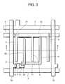
- FIG. 3is a plan view of one pixel portion of a TFT substrate of a liquid crystal display device according to the present invention.
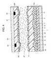
- FIG. 4is a cross-sectional view taken along the line X-X′ of FIG. 3.
- a metal film (of Cr, Al, or Ta, or an alloy of the foregoing metals) having a thickness of 200 to 500 nmis patterned on a transparent insulation substrate 1 formed of, for example, glass in order to simultaneously form a scanning line 3 , a gate electrode 2 connected to the scanning line 3 , and a common line 4 .
- a gate insulating film 6(such as an SiNx film having a thickness of 400 to 600 nm) is formed over the substrate.
- a semiconductor island 7(of, for example, amorphous silicon or polysilicon) is formed on the gate insulating film 6 .
- a metal film(of Cr, Al, or Ta, or an alloy of the foregoing metals) having a thickness of 200 to 500 nm is deposited and then patterned in order to form a signal line 10 , source/drain electrodes 8 , 9 , and a first pixel electrode 11 (lower layer pixel electrode) connected to the source/drain electrode 9 .
- the first pixel electrode 11is formed to include a capacitive electrode 22 overlapping the common line 4 in addition to electrodes parallel to later formed common electrodes 5 .
- the common line 4 and the capacitive electrode 22form an auxiliary capacitor.
- the lower-layer pixel electrodealso serves as a capacitive storage electrode.
- a metal film (of Cr, Al, or Ta, or an alloy of the foregoing metals) having a thickness of 20 to 120 nmis deposited as a film thinner than the signal line 10 over the first interlayer insulating film 12 , preferably to a thickness of twentieth to third of the thickness of the signal line 10 , and then patterned to form the common electrodes 5 connected to the common line 4 through the contact hole 31 for common electrode and a second pixel electrode 25 (upper-layer pixel electrode) connected to the source/drain electrode 9 through the contact hole 32 for pixel electrode.
- a lower limit of the thickness of the common electrodes 5 and the second pixel electrode 25is based on a desired ratio of resistance of the common electrode (and the upper-layer pixel electrode) to resistance of the common line (and the signal line).
- An upper limit of the thickness thereofis based on a desired height of the step formed by the insulating film below the alignment layer.
- the common electrodes 5 and the second pixel electrode 25are formed in parallel with each other and, in addition, the common electrodes 5 and the first pixel electrode 11 are formed in parallel with each other. Furthermore, the second pixel electrode 25 is formed so as not to overlap the first pixel electrode 11 .
- An opposing substrate 200 disposed opposite the TFT substrate 100is generally formed in the following manner.
- a light shielding film 52is formed on a transparent insulation substrate 51 so that the film partitions the individual pixels of the TFT substrate 100 and corresponds to the semiconductor island 7 . Then, an insulating film 53 and an alignment layer 54 are formed over the substrate to cover the light shielding film 52 .
- Liquid crystal 27is filled between thus formed TFT substrate 100 and opposing substrate 200 to provide a liquid crystal display device.
- a polarizer, etc.are not shown for simplicity.
- the second pixel electrode 25 , the common electrodes 5 , etc.are formed in the layer different from the layer used for the signal line 10 and the common line 4 that allow a large amount of current.
- the thickness of the metal film constituting the second pixel electrode 25 and the common electrodes 5can be determined independently of the thickness of the signal line, the common line, etc. Consequently, the metal film constituting the pixel electrode and the common electrode can be formed to a thickness thinner than the signal line, the common line, etc., thereby allowing reduction of height of steps formed by the surface of the second interlayer insulating film 26 located on the metal film.
- one set of the common electrodes 5 and the second pixel electrode 25 for generating the lateral electric fieldis formed of the metal film having a thickness of 20 to 120 nm, which thickness is significantly smaller than that of the conventional metal film, i.e., 200 to 500 nm, and in addition, has thereunder no lines and electrodes that produce height of steps, thereby allowing the second interlayer insulating film 26 to significantly reduce height of its steps, which height is significantly smaller than that observed in the conventional case.
- the first pixel electrode 11is still thick, i.e., 200 to 500 nm.
- the first interlayer insulating film 12 and the second interlayer insulating film 26are formed over the substrate to cover the other set of the electrodes, height of steps formed below the alignment layer 13 is significantly smaller than that observed in the conventional structure. Accordingly, a material for the alignment layer is formed with high flatness on the second interlayer insulating film 26 and the material can be uniformly rubbed in a subsequent step, thereby allowing uniformity of the alignment layer 13 over the substrate.
- the liquid crystal display device including the above-described uniform alignment layersexhibits noticeable advantages, particularly, when the display device is used as a liquid crystal display device performing monochromatic display.
- the contrast obtained by dividing the white luminance by the black luminancehas been proven to increase 1.5 times that observed using the liquid crystal display apparatus having the structure shown in FIGS. 1 and 2.
- the second interlayer insulating filmis formed thicker than the first interlayer insulating film
- the second interlayer insulating filmmay be formed thinner than the above-described thickness depending on a contrast allowed in a liquid crystal display device.
- the second interlayer insulating filmmay be formed using an organic film instead of the inorganic film, allowing the second interlayer insulating film to be thinner than the first interlayer insulating film.
- the major electrodes for generating the lateral electric fieldare formed in a layer different from layers for other electrodes and lines, and further, formed thinner than the other electrodes and lines. Therefore, flatness of an underlying film for an alignment layer is significantly improved and a material for the alignment layer also can be formed with high flatness on the underlying film, and further, rubbing of the alignment layer material can therefore be performed uniformly over the substrate. Consequently, the uniformly rubbed alignment layer is obtained and the liquid crystal display device is able to significantly enhance its contrast.
Landscapes
- Physics & Mathematics (AREA)
- Nonlinear Science (AREA)
- Mathematical Physics (AREA)
- Chemical & Material Sciences (AREA)
- Crystallography & Structural Chemistry (AREA)
- General Physics & Mathematics (AREA)
- Optics & Photonics (AREA)
- Geometry (AREA)
- Liquid Crystal (AREA)
- Thin Film Transistor (AREA)
- Devices For Indicating Variable Information By Combining Individual Elements (AREA)
Abstract
Description
- 1. Field of the Invention[0001]
- The present invention relates to a lateral electric field liquid crystal display device. More specifically, the present invention relates to an electrode structure of an active element substrate.[0002]
- 2. Description of the Related Art[0003]
- In general, a lateral electric field liquid crystal display device is constructed such that a pixel electrode and a common electrode are provided on the same, substrate, and an electric field is applied therebetween. Each pixel electrode is connected to an active element, such as a thin-film transistor (TFT), to constitute an active matrix substrate (TFT substrate). Liquid crystal is filled between the TFT substrate and an opposing substrate. In this lateral electric field liquid crystal display device, since the liquid crystal is controlled by the electric field applied parallel to a substrate surface, a wide viewing angle can be obtained.[0004]
- The TFT substrate of the type described above will be explained with reference to FIGS. 1 and 2. FIG. 1 is a plan view of one pixel of the TFT substrate of the conventional liquid crystal display device as viewed from the side of liquid crystal. FIG. 2 is a cross-sectional view taken along the line X-X′ of FIG. 1.[0005]
- A[0006]
scanning line 103, agate electrode 102 connected to thescanning line 103, acommon line 104, and acommon electrode 105 extending as a part of thecommon line 104 are formed of a metal film in the same layer on atransparent insulation substrate 101 formed of, for example, glass. Agate insulating film 106 is formed over these lines and electrodes. Thecommon electrode 105 is partially formed parallel to a pixel electrode described below. Subsequently, asemiconductor island 107 is formed on thegate insulating film 106. Thereafter, asignal line 110, source/drain electrodes semiconductor island 107 to be connected thereto, and apixel electrode 111 connected to the source/drain electrode 109 are formed using the same metal film as that used to form the source/drain electrode. Note that both thepixel electrode 111 and the previously formedcommon electrode 105 are partially formed in parallel with each other. In addition, an interlayerinsulating film 112 and analignment layer 113 are formed in such a manner as to cover thesemiconductor island 107, the source/drain electrodes pixel electrode 111. In this manner, formation ofTFT substrate 300 is completed. Note that a storage capacitor is formed where thepixel electrode 111 and thecommon line 104 overlap each other (anoverlap portion 122 indicated as a cross-hatched portion). - [0007]
Light shielding film 152 is formed on thetransparent insulation substrate 151 to partition pixels on theTFT substrate 300 and cover thesemiconductor island 107. Aninsulating film 153 and analignment layer 154 are formed to cover thelight shielding films 152, thereby constituting anopposing substrate 400. - [0008]
Liquid crystal 127 is filled between theTFT substrate 300 and theopposing substrate 400 thus to form a liquid crystal display device. In FIG. 2, a polarizer and the like are not shown for simplification. - It should be note that the[0009]
scanning line 103, thecommon line 104 and thesignal line 110 are formed to have enough thickness to reduce resistance values thereof. Since thecommon line 104 and thecommon electrode 105 are formed together with thescanning line 103, all of which have the same thickness. Consequently, as shown in FIG. 2, theinterlayer insulating film 112 covering these electrodes and lines is formed with large variation in a height of step. In this case, when an alignment layer material coated having large height of step on theinterlayer insulating film 112 is subjected to a rubbing process, the material cannot be rubbed uniformly over the TFT substrate. As a consequence, thealignment layer 113 is formed unevenly due to nonuniformity of rubbing, thereby making the liquid crystal display device have nonuniformity of display. - An object of the present invention is therefore to provide a lateral electric field liquid crystal display device configured to have an insulating film formed below an alignment layer and with reduced height of its steps in order to perform rubbing uniformly over the alignment layer.[0010]
- According to the present invention, there is provided a lateral electric field liquid crystal display device including a TFT substrate, an opposing substrate and a liquid crystal layer sandwiched between the TFT substrate and the opposing substrate, in which the TFT substrate includes a signal line, a common line, a pixel electrode and a common electrode. The liquid crystal display device thus configured is characterized in that the pixel electrode is partially formed in a layer different from and above the signal line and the common line, the common electrode is formed in the layer, and the common electrode and a portion of the pixel electrode formed in the layer is formed thinner than the signal line and the common line.[0011]
- The liquid crystal display device thus configured is further characterized in that the pixel electrode further comprises an auxiliary capacitive electrode formed in the same layer as that used for the signal line and formed to overlap the common line.[0012]
- The liquid crystal display device thus configured is further characterized in that the portion of the pixel electrode is connected to a drain electrode of a thin film transistor (TFT) through a contact hole and the common electrode is connected to the common line through a contact hole.[0013]
- The liquid crystal display device thus configured is still further characterized in that the TFT substrate further includes a transparent substrate, a scanning line formed on the transparent substrate, a gate insulating film formed on the transparent substrate to cover the scanning line, a semiconductor layer formed on the gate insulating film, a first interlayer insulating film formed on the gate insulating film to cover the semiconductor film, a second insulating film formed on the first insulating film, and an alignment layer formed on the second insulating film. The above-described liquid crystal display device is further constructed such that the common line is formed on the transparent substrate together with the scanning line, the signal line is formed between the gate insulating film and the first interlayer insulating film and is connected to one end of the semiconductor film, the pixel electrode includes a lower-layer pixel electrode formed on the gate insulating film together with the signal line and connected to the other end of the semiconductor film, the common electrode is formed between the first interlayer insulating film and the second interlayer insulating film and connected to the common line, the pixel electrode further includes an upper-layer pixel electrode formed on the first interlayer insulating film together with the common electrode and connected to the lower-layer pixel electrode, and the upper-layer pixel electrode is thinner than the signal line and the common line.[0014]
- The liquid crystal display device thus constructed is further characterized in that a thickness of each of the common electrode and the upper-layer pixel electrode is in a range of twentieth to third of a thickness of each of the signal line and the common line.[0015]
- Therefore, flatness of an underlying film for an alignment layer is significantly improved and a material for the alignment layer also can be formed with high flatness on the underlying film, and further, rubbing of the material for the alignment layer can therefore be performed uniformly over the substrate. Consequently, the uniformly rubbed alignment layer is obtained and the liquid crystal display device is able to significantly reduce display failure due to unevenness of rubbing.[0016]
- In the accompanying drawings:[0017]
- FIG. 1 is a plan view of one pixel portion of a TFT substrate of a conventional liquid crystal display device;[0018]
- FIG. 2 is a cross-sectional view taken along the line X-X′ of FIG. 1;[0019]
- FIG. 3 is a plan view of one pixel portion of a TFT substrate of a liquid crystal display device according to the present invention; and[0020]
- FIG. 4 is a cross-sectional view taken along the line X-X′ of FIG. 3.[0021]
- Hereinbelow, an embodiment of a liquid crystal display device according to the present invention will be described with reference to FIGS. 3 and 4.[0022]
- A metal film (of Cr, Al, or Ta, or an alloy of the foregoing metals) having a thickness of 200 to 500 nm is patterned on a[0023]
transparent insulation substrate 1 formed of, for example, glass in order to simultaneously form ascanning line 3, agate electrode 2 connected to thescanning line 3, and acommon line 4. Thereafter, a gate insulating film6 (such as an SiNx film having a thickness of 400 to 600 nm) is formed over the substrate. Then, a semiconductor island7 (of, for example, amorphous silicon or polysilicon) is formed on thegate insulating film 6. Thereafter, a metal film (of Cr, Al, or Ta, or an alloy of the foregoing metals) having a thickness of 200 to 500 nm is deposited and then patterned in order to form asignal line 10, source/drain electrodes drain electrode 9. As shown in FIG. 3, thefirst pixel electrode 11 is formed to include acapacitive electrode 22 overlapping thecommon line 4 in addition to electrodes parallel to later formedcommon electrodes 5. Thecommon line 4 and thecapacitive electrode 22 form an auxiliary capacitor. Thus, the lower-layer pixel electrode also serves as a capacitive storage electrode. - A first[0024]
interlayer insulating film 12 of, for example, SiNx, having a thickness of 200 to 400 nm is deposited over the substrate to cover thesemiconductor island 7, the source/drain electrodes signal line 10, and thefirst pixel electrode 11. Subsequently, acontact hole 31 for common electrode and acontact hole 32 for pixel electrode are formed in the insulating film so that portions of the insulating film positioned above thecommon line 4 and the source/drain electrode 9 are opened. - A metal film (of Cr, Al, or Ta, or an alloy of the foregoing metals) having a thickness of 20 to 120 nm is deposited as a film thinner than the[0025]
signal line 10 over the firstinterlayer insulating film 12, preferably to a thickness of twentieth to third of the thickness of thesignal line 10, and then patterned to form thecommon electrodes 5 connected to thecommon line 4 through thecontact hole 31 for common electrode and a second pixel electrode25 (upper-layer pixel electrode) connected to the source/drain electrode 9 through thecontact hole 32 for pixel electrode. In this case, a lower limit of the thickness of thecommon electrodes 5 and thesecond pixel electrode 25 is based on a desired ratio of resistance of the common electrode (and the upper-layer pixel electrode) to resistance of the common line (and the signal line). An upper limit of the thickness thereof is based on a desired height of the step formed by the insulating film below the alignment layer. Thecommon electrodes 5 and thesecond pixel electrode 25 are formed in parallel with each other and, in addition, thecommon electrodes 5 and thefirst pixel electrode 11 are formed in parallel with each other. Furthermore, thesecond pixel electrode 25 is formed so as not to overlap thefirst pixel electrode 11. - A second[0026]
interlayer insulating film 26 made of, for example, SiNx and having a thickness of 600 to 800 nm is deposited over the substrate to cover thecommon electrodes 5 and thesecond pixel electrode 25. Subsequently, a material for an alignment layer is coated thereon to a thickness of 80 to 120 nm and then rubbed to form analignment layer 13. In this manner, formation ofTFT substrate 100 is completed. - An opposing[0027]
substrate 200 disposed opposite theTFT substrate 100 is generally formed in the following manner. - First, a[0028]
light shielding film 52 is formed on atransparent insulation substrate 51 so that the film partitions the individual pixels of theTFT substrate 100 and corresponds to thesemiconductor island 7. Then, an insulatingfilm 53 and analignment layer 54 are formed over the substrate to cover thelight shielding film 52. - [0029]
Liquid crystal 27 is filled between thus formedTFT substrate 100 and opposingsubstrate 200 to provide a liquid crystal display device. In FIG. 4, a polarizer, etc., are not shown for simplicity. - As described above, the[0030]
second pixel electrode 25, thecommon electrodes 5, etc. are formed in the layer different from the layer used for thesignal line 10 and thecommon line 4 that allow a large amount of current. Thus, the thickness of the metal film constituting thesecond pixel electrode 25 and thecommon electrodes 5 can be determined independently of the thickness of the signal line, the common line, etc. Consequently, the metal film constituting the pixel electrode and the common electrode can be formed to a thickness thinner than the signal line, the common line, etc., thereby allowing reduction of height of steps formed by the surface of the secondinterlayer insulating film 26 located on the metal film. - As described above, one set of the[0031]
common electrodes 5 and thesecond pixel electrode 25 for generating the lateral electric field is formed of the metal film having a thickness of 20 to 120 nm, which thickness is significantly smaller than that of the conventional metal film, i.e., 200 to 500 nm, and in addition, has thereunder no lines and electrodes that produce height of steps, thereby allowing the secondinterlayer insulating film 26 to significantly reduce height of its steps, which height is significantly smaller than that observed in the conventional case. - As for the other set of the[0032]
common electrodes 5 and thefirst pixel electrode 11 for generating the lateral field, thefirst pixel electrode 11 is still thick, i.e., 200 to 500 nm. However, since the firstinterlayer insulating film 12 and the secondinterlayer insulating film 26 are formed over the substrate to cover the other set of the electrodes, height of steps formed below thealignment layer 13 is significantly smaller than that observed in the conventional structure. Accordingly, a material for the alignment layer is formed with high flatness on the secondinterlayer insulating film 26 and the material can be uniformly rubbed in a subsequent step, thereby allowing uniformity of thealignment layer 13 over the substrate. - The liquid crystal display device including the above-described uniform alignment layers exhibits noticeable advantages, particularly, when the display device is used as a liquid crystal display device performing monochromatic display. In this case, the contrast obtained by dividing the white luminance by the black luminance has been proven to increase 1.5 times that observed using the liquid crystal display apparatus having the structure shown in FIGS. 1 and 2.[0033]
- In the embodiment, although the second interlayer insulating film is formed thicker than the first interlayer insulating film, the second interlayer insulating film may be formed thinner than the above-described thickness depending on a contrast allowed in a liquid crystal display device. In addition, the second interlayer insulating film may be formed using an organic film instead of the inorganic film, allowing the second interlayer insulating film to be thinner than the first interlayer insulating film.[0034]
- The present embodiment has been described with reference to the example including the storage electrode. However, even in the structure including no storage electrode, it is apparent that equivalent advantages can be obtained by providing pixel electrodes and common electrodes in a layer different from those for the signal and common lines.[0035]
- As described above, according to the liquid crystal display device of the present invention, the major electrodes for generating the lateral electric field are formed in a layer different from layers for other electrodes and lines, and further, formed thinner than the other electrodes and lines. Therefore, flatness of an underlying film for an alignment layer is significantly improved and a material for the alignment layer also can be formed with high flatness on the underlying film, and further, rubbing of the alignment layer material can therefore be performed uniformly over the substrate. Consequently, the uniformly rubbed alignment layer is obtained and the liquid crystal display device is able to significantly enhance its contrast.[0036]
Claims (8)
1. A lateral electric field liquid crystal display device comprising:
a TFT substrate provided with a signal line, a common line, a pixel electrode and a common electrode, said pixel electrode being partially formed in a layer different from and above said signal line and said common line, said common electrode being formed in said layer; said common electrode and a portion of said pixel electrode formed in said layer being formed thinner than said signal line and said common line;
an opposing substrate; and
a liquid crystal layer sandwiched between said TFT substrate and said opposing substrate,
said TFT substrate including.
2. The lateral electric field liquid crystal display device according toclaim 1 , wherein the pixel electrode further comprises an auxiliary capacitive electrode formed in the same layer as that used for said signal line and formed to overlap said common line.
3. The lateral electric field liquid crystal display device according toclaim 1 , wherein said portion of said pixel electrode is connected to a drain electrode of a thin film transistor (TFT) through a contact hole and said common electrode is connected to said common line through a contact hole.
4. A lateral electric field liquid crystal display device according toclaim 1 , wherein said TFT substrate further comprises:
a transparent substrate;
a scanning line formed on said transparent substrate;
a gate insulating film formed on said transparent substrate to cover said scanning line;
a semiconductor layer formed on said gate insulating film;
a first interlayer insulating film formed on said gate insulating film to cover said semiconductor film;
a second insulating film formed on said first insulating film; and
an alignment layer formed on said second insulating film,
and wherein said common line is formed on said transparent substrate together with said scanning line, and wherein said signal line is formed between said gate insulating film and said first interlayer insulating film and is connected to one end of said semiconductor film, and wherein said pixel electrode includes a lower-layer pixel electrode formed on said gate insulating film together with said signal line and connected to the other end of said semiconductor film, and wherein said common electrode is formed between said first interlayer insulating film and said second interlayer insulating film and connected to said common line, and wherein said pixel electrode further includes an upper-layer pixel electrode formed on said first interlayer insulating film together with said common electrode and connected to said lower-layer pixel electrode, and wherein said upper-layer pixel electrode is thinner than said signal line and said common line.
5. The lateral electric field liquid crystal display device according toclaim 4 , wherein a thickness of each of said common electrode and said upper-layer pixel electrode is in a range of twentieth to third of a thickness of each of said signal line and said common line.
6. The lateral electric field liquid crystal display device according toclaim 4 , wherein a voltage is applied between said common electrode and said upper-layer pixel electrode and between said common electrode and said lower-layer pixel electrode to make liquid crystal molecules of said liquid crystal layer rotate within a plane parallel to said transparent substrate.
7. The lateral electric field liquid crystal display device according toclaim 4 , wherein a portion of said lower-layer pixel electrode is an auxiliary capacitive electrode.
8. The lateral electric field liquid crystal display device according toclaim 1 , wherein a portion of said pixel electrode formed in said layer is connected to a source/drain electrode of a thin film transistor through a contact hole and said common electrode is connected to said common line through a contact hole.
Applications Claiming Priority (2)
| Application Number | Priority Date | Filing Date | Title |
|---|---|---|---|
| JP21184/2002 | 2002-01-30 | ||
| JP2002021184AJP3586674B2 (en) | 2002-01-30 | 2002-01-30 | Liquid crystal display |
Publications (2)
| Publication Number | Publication Date |
|---|---|
| US20030142259A1true US20030142259A1 (en) | 2003-07-31 |
| US6888601B2 US6888601B2 (en) | 2005-05-03 |
Family
ID=27606306
Family Applications (1)
| Application Number | Title | Priority Date | Filing Date |
|---|---|---|---|
| US10/353,023Expired - LifetimeUS6888601B2 (en) | 2002-01-30 | 2003-01-29 | Lateral electric field liquid crystal display device |
Country Status (5)
| Country | Link |
|---|---|
| US (1) | US6888601B2 (en) |
| JP (1) | JP3586674B2 (en) |
| KR (1) | KR100510564B1 (en) |
| CN (1) | CN1252526C (en) |
| TW (1) | TWI225569B (en) |
Cited By (6)
| Publication number | Priority date | Publication date | Assignee | Title |
|---|---|---|---|---|
| US20050200791A1 (en)* | 2004-03-11 | 2005-09-15 | Lg.Philips Lcd Co., Ltd. | In-plane switching mode liquid crystal display device and fabrication method thereof |
| US20070133031A1 (en)* | 2005-12-08 | 2007-06-14 | Canon Kabushiki Kaisha | Image processing apparatus and image processing method |
| US20110141421A1 (en)* | 2009-12-11 | 2011-06-16 | Sang-Wook Lee | Liquid crystal display device |
| US20120169984A1 (en)* | 2010-12-31 | 2012-07-05 | Samsung Electronics Co., Ltd. | Display substrate and method of manufacturing the same |
| CN103018979A (en)* | 2012-12-21 | 2013-04-03 | 昆山龙腾光电有限公司 | Blue phase liquid crystal display device |
| JP2018128691A (en)* | 2006-04-06 | 2018-08-16 | 株式会社半導体エネルギー研究所 | Display device |
Families Citing this family (7)
| Publication number | Priority date | Publication date | Assignee | Title |
|---|---|---|---|---|
| JP2003228081A (en) | 2002-01-31 | 2003-08-15 | Nec Corp | Liquid crystal display device and manufacturing method therefor |
| US7916254B2 (en)* | 2003-10-27 | 2011-03-29 | Hitachi Displays, Ltd. | Liquid crystal display apparatus for performing alignment process by irradiating light |
| KR101046923B1 (en)* | 2004-02-02 | 2011-07-06 | 삼성전자주식회사 | Thin film transistor array panel and liquid crystal display including the same |
| KR20060077870A (en)* | 2004-12-31 | 2006-07-05 | 엘지.필립스 엘시디 주식회사 | Transverse electric field liquid crystal display device |
| CN100417995C (en)* | 2005-10-10 | 2008-09-10 | 友达光电股份有限公司 | Wire substrate of liquid crystal display and manufacturing method thereof |
| JP2008090279A (en)* | 2006-09-04 | 2008-04-17 | Epson Imaging Devices Corp | Liquid crystal display and electronic apparatus |
| JP2008242262A (en)* | 2007-03-28 | 2008-10-09 | Tpo Displays Corp | Substrate of liquid crystal display device, and method of manufacturing the same |
Citations (4)
| Publication number | Priority date | Publication date | Assignee | Title |
|---|---|---|---|---|
| US5598285A (en)* | 1992-09-18 | 1997-01-28 | Hitachi, Ltd. | Liquid crystal display device |
| US6049369A (en)* | 1995-09-11 | 2000-04-11 | Hitachi, Ltd. | Parallel-field TFT LCD having reference electrodes and a conductive layer |
| US6208399B1 (en)* | 1997-04-11 | 2001-03-27 | Hitachi, Ltd. | Liquid crystal display device |
| US6697141B2 (en)* | 1999-06-11 | 2004-02-24 | Matsushita Electric Industrial Co., Ltd. | Liquid crystal display with opaque common electrodes over the video signal lines and fabrication method thereof |
Family Cites Families (8)
| Publication number | Priority date | Publication date | Assignee | Title |
|---|---|---|---|---|
| JP2701698B2 (en)* | 1993-07-20 | 1998-01-21 | 株式会社日立製作所 | Liquid crystal display |
| JP3597305B2 (en)* | 1996-03-05 | 2004-12-08 | 株式会社半導体エネルギー研究所 | Liquid crystal display device and manufacturing method thereof |
| JP3788649B2 (en)* | 1996-11-22 | 2006-06-21 | 株式会社半導体エネルギー研究所 | Liquid crystal display |
| JP4036498B2 (en)* | 1997-03-21 | 2008-01-23 | 松下電器産業株式会社 | Active matrix liquid crystal display device |
| KR100477130B1 (en) | 1997-09-25 | 2005-08-29 | 삼성전자주식회사 | Thin Film Transistor Board and Manufacturing Method of Flat Drive Liquid Crystal Display |
| JP3099816B2 (en)* | 1998-08-12 | 2000-10-16 | 日本電気株式会社 | Active matrix type liquid crystal display |
| KR100303440B1 (en) | 1998-11-02 | 2002-10-25 | 삼성전자 주식회사 | Liquid crystal display of in-plane switching mode |
| JP3577625B2 (en)* | 1998-11-26 | 2004-10-13 | 株式会社アドバンスト・ディスプレイ | Manufacturing method of liquid crystal display device |
- 2002
- 2002-01-30JPJP2002021184Apatent/JP3586674B2/ennot_activeExpired - Lifetime
- 2003
- 2003-01-22TWTW092101327Apatent/TWI225569B/ennot_activeIP Right Cessation
- 2003-01-29USUS10/353,023patent/US6888601B2/ennot_activeExpired - Lifetime
- 2003-01-29KRKR10-2003-0005758Apatent/KR100510564B1/ennot_activeExpired - Fee Related
- 2003-01-30CNCNB031031285Apatent/CN1252526C/ennot_activeExpired - Lifetime
Patent Citations (4)
| Publication number | Priority date | Publication date | Assignee | Title |
|---|---|---|---|---|
| US5598285A (en)* | 1992-09-18 | 1997-01-28 | Hitachi, Ltd. | Liquid crystal display device |
| US6049369A (en)* | 1995-09-11 | 2000-04-11 | Hitachi, Ltd. | Parallel-field TFT LCD having reference electrodes and a conductive layer |
| US6208399B1 (en)* | 1997-04-11 | 2001-03-27 | Hitachi, Ltd. | Liquid crystal display device |
| US6697141B2 (en)* | 1999-06-11 | 2004-02-24 | Matsushita Electric Industrial Co., Ltd. | Liquid crystal display with opaque common electrodes over the video signal lines and fabrication method thereof |
Cited By (13)
| Publication number | Priority date | Publication date | Assignee | Title |
|---|---|---|---|---|
| US8125609B2 (en)* | 2004-03-11 | 2012-02-28 | Lg Display Co., Ltd. | In-plane switching mode liquid crystal display device with multi-layer electrode and fabrication method thereof |
| US20050200791A1 (en)* | 2004-03-11 | 2005-09-15 | Lg.Philips Lcd Co., Ltd. | In-plane switching mode liquid crystal display device and fabrication method thereof |
| US20070133031A1 (en)* | 2005-12-08 | 2007-06-14 | Canon Kabushiki Kaisha | Image processing apparatus and image processing method |
| US11073729B2 (en) | 2006-04-06 | 2021-07-27 | Semiconductor Energy Laboratory Co., Ltd. | Liquid crystal display device, semiconductor device, and electronic appliance |
| JP2018128691A (en)* | 2006-04-06 | 2018-08-16 | 株式会社半導体エネルギー研究所 | Display device |
| US10684517B2 (en) | 2006-04-06 | 2020-06-16 | Semiconductor Energy Laboratory Co., Ltd. | Liquid crystal display device, semiconductor device, and electronic appliance |
| US11442317B2 (en) | 2006-04-06 | 2022-09-13 | Semiconductor Energy Laboratory Co., Ltd. | Liquid crystal display device, semiconductor device, and electronic appliance |
| US11644720B2 (en) | 2006-04-06 | 2023-05-09 | Semiconductor Energy Laboratory Co., Ltd. | Liquid crystal display device, semiconductor device, and electronic appliance |
| US11921382B2 (en) | 2006-04-06 | 2024-03-05 | Semiconductor Energy Laboratory Co., Ltd. | Liquid crystal display device, semiconductor device, and electronic appliance |
| US8848156B2 (en)* | 2009-12-11 | 2014-09-30 | Lg Display Co., Ltd. | Liquid crystal display device |
| US20110141421A1 (en)* | 2009-12-11 | 2011-06-16 | Sang-Wook Lee | Liquid crystal display device |
| US20120169984A1 (en)* | 2010-12-31 | 2012-07-05 | Samsung Electronics Co., Ltd. | Display substrate and method of manufacturing the same |
| CN103018979A (en)* | 2012-12-21 | 2013-04-03 | 昆山龙腾光电有限公司 | Blue phase liquid crystal display device |
Also Published As
| Publication number | Publication date |
|---|---|
| TWI225569B (en) | 2004-12-21 |
| CN1252526C (en) | 2006-04-19 |
| US6888601B2 (en) | 2005-05-03 |
| KR20030065396A (en) | 2003-08-06 |
| JP3586674B2 (en) | 2004-11-10 |
| CN1435719A (en) | 2003-08-13 |
| JP2003222903A (en) | 2003-08-08 |
| TW200302385A (en) | 2003-08-01 |
| KR100510564B1 (en) | 2005-08-26 |
Similar Documents
| Publication | Publication Date | Title |
|---|---|---|
| US7671931B2 (en) | Liquid crystal display device and method of fabricating the same | |
| US5771083A (en) | Active matrix substrate and liquid crystal display device | |
| US7508471B2 (en) | Transflective liquid crystal display | |
| US7420213B2 (en) | Thin film transistor array substrate having main gate insulating film formed of organic material and sub gate insulating film formed of ferroelectric material and fabricating method thereof | |
| US6888601B2 (en) | Lateral electric field liquid crystal display device | |
| JP2001013520A (en) | Active matrix type liquid crystal display | |
| US5168074A (en) | Active matrix liquid crystal display fabrication for grayscale | |
| US6597420B2 (en) | Liquid crystal display device having color film on a first substrate and a method for manufacturing the same | |
| US8115215B2 (en) | Array substrate and method for manufacturing the same | |
| US20160178981A1 (en) | Fringe field switching mode liquid crystal display device | |
| US6924864B2 (en) | Array substrate for in-plane switching mode liquid crystal display device and method of fabricating the same | |
| WO2017124686A1 (en) | Tft array substrate structure and manufacturing method thereof | |
| US5546205A (en) | Active matrix liquid crystal display panel having compensating capacitor provided without lowering pixel aperture ratio | |
| WO2019082465A1 (en) | Display device and method for manufacturing same | |
| WO2018223430A1 (en) | Array substrate, manufacturing method thereof, and display panel | |
| US9564459B2 (en) | Liquid crystal display panel and method for manufacturing liquid crystal display panel | |
| US20050110915A1 (en) | Pixel and method for pixel repair | |
| US20060132682A1 (en) | Thin film transistor array panel and liquid crystal display including the panel | |
| CN109427874B (en) | Display device and method of manufacturing the same | |
| US20060157705A1 (en) | Thin film transistor array panel | |
| WO2016061995A1 (en) | Preparation method for array substrate, array substrate and display device | |
| US6046063A (en) | Method of manufacturing liquid crystal display | |
| JP4154880B2 (en) | Electro-optical device and manufacturing method thereof | |
| JP3176091B2 (en) | Thin film transistor | |
| US20060250562A1 (en) | Liquid crystal display panel, active matrix substrate and fabricating mehod |
Legal Events
| Date | Code | Title | Description |
|---|---|---|---|
| AS | Assignment | Owner name:NEC CORPORATION, JAPAN Free format text:ASSIGNMENT OF ASSIGNORS INTEREST;ASSIGNORS:ASAI, TAKUYA;KUROHA, SYOUICHI;SASAKI, TAKESHI;REEL/FRAME:013720/0762 Effective date:20030120 | |
| AS | Assignment | Owner name:NEC LCD TECHNOLOGIES, LTD, JAPAN Free format text:ASSIGNMENT OF ASSIGNORS INTEREST;ASSIGNOR:NEC CORPORATION;REEL/FRAME:013989/0395 Effective date:20030401 | |
| FEPP | Fee payment procedure | Free format text:PAYOR NUMBER ASSIGNED (ORIGINAL EVENT CODE: ASPN); ENTITY STATUS OF PATENT OWNER: LARGE ENTITY | |
| STCF | Information on status: patent grant | Free format text:PATENTED CASE | |
| FPAY | Fee payment | Year of fee payment:4 | |
| AS | Assignment | Owner name:NLT TECHNOLOGIES, LTD., JAPAN Free format text:CHANGE OF NAME;ASSIGNOR:NEC LCD TECHNOLOGIES, LTD.;REEL/FRAME:027189/0038 Effective date:20110701 | |
| FPAY | Fee payment | Year of fee payment:8 | |
| FPAY | Fee payment | Year of fee payment:12 |