US20030137888A1 - Techniques of recovering data from memory cells affected by field coupling with adjacent memory cells - Google Patents
Techniques of recovering data from memory cells affected by field coupling with adjacent memory cellsDownload PDFInfo
- Publication number
- US20030137888A1 US20030137888A1US10/357,840US35784003AUS2003137888A1US 20030137888 A1US20030137888 A1US 20030137888A1US 35784003 AUS35784003 AUS 35784003AUS 2003137888 A1US2003137888 A1US 2003137888A1
- Authority
- US
- United States
- Prior art keywords
- memory cells
- levels
- storage elements
- charge
- group
- Prior art date
- Legal status (The legal status is an assumption and is not a legal conclusion. Google has not performed a legal analysis and makes no representation as to the accuracy of the status listed.)
- Granted
Links
- 230000015654memoryEffects0.000titleclaimsabstractdescription142
- 238000000034methodMethods0.000titleclaimsabstractdescription54
- 230000008878couplingEffects0.000titleclaimsdescription16
- 238000010168coupling processMethods0.000titleclaimsdescription16
- 238000005859coupling reactionMethods0.000titleclaimsdescription16
- 238000003860storageMethods0.000claimsdescription104
- 230000000694effectsEffects0.000claimsdescription8
- 230000015556catabolic processEffects0.000abstract1
- 238000006731degradation reactionMethods0.000abstract1
- 238000009826distributionMethods0.000description31
- 230000008569processEffects0.000description10
- 238000003491arrayMethods0.000description9
- 238000011084recoveryMethods0.000description9
- 230000008859changeEffects0.000description5
- 230000007480spreadingEffects0.000description4
- 238000003892spreadingMethods0.000description4
- 230000009471actionEffects0.000description2
- 238000013500data storageMethods0.000description2
- 239000003989dielectric materialSubstances0.000description2
- 230000003252repetitive effectEffects0.000description2
- 238000004364calculation methodMethods0.000description1
- 230000007423decreaseEffects0.000description1
- 230000003247decreasing effectEffects0.000description1
- 238000010586diagramMethods0.000description1
- 238000004193electrokinetic chromatographyMethods0.000description1
- 230000006870functionEffects0.000description1
- 239000011810insulating materialSubstances0.000description1
- 238000004519manufacturing processMethods0.000description1
- 230000004044responseEffects0.000description1
- 239000004065semiconductorSubstances0.000description1
- 239000000758substrateSubstances0.000description1
Images


Classifications
- G—PHYSICS
- G11—INFORMATION STORAGE
- G11C—STATIC STORES
- G11C16/00—Erasable programmable read-only memories
- G11C16/02—Erasable programmable read-only memories electrically programmable
- G11C16/06—Auxiliary circuits, e.g. for writing into memory
- G11C16/26—Sensing or reading circuits; Data output circuits
- G—PHYSICS
- G11—INFORMATION STORAGE
- G11C—STATIC STORES
- G11C16/00—Erasable programmable read-only memories
- G11C16/02—Erasable programmable read-only memories electrically programmable
- G11C16/06—Auxiliary circuits, e.g. for writing into memory
- G11C16/34—Determination of programming status, e.g. threshold voltage, overprogramming or underprogramming, retention
- G11C16/3418—Disturbance prevention or evaluation; Refreshing of disturbed memory data
- G11C16/3431—Circuits or methods to detect disturbed nonvolatile memory cells, e.g. which still read as programmed but with threshold less than the program verify threshold or read as erased but with threshold greater than the erase verify threshold, and to reverse the disturbance via a refreshing programming or erasing step
- G—PHYSICS
- G11—INFORMATION STORAGE
- G11C—STATIC STORES
- G11C11/00—Digital stores characterised by the use of particular electric or magnetic storage elements; Storage elements therefor
- G11C11/56—Digital stores characterised by the use of particular electric or magnetic storage elements; Storage elements therefor using storage elements with more than two stable states represented by steps, e.g. of voltage, current, phase, frequency
- G11C11/5621—Digital stores characterised by the use of particular electric or magnetic storage elements; Storage elements therefor using storage elements with more than two stable states represented by steps, e.g. of voltage, current, phase, frequency using charge storage in a floating gate
- G11C11/5642—Sensing or reading circuits; Data output circuits
- G—PHYSICS
- G11—INFORMATION STORAGE
- G11C—STATIC STORES
- G11C16/00—Erasable programmable read-only memories
- G11C16/02—Erasable programmable read-only memories electrically programmable
- G11C16/06—Auxiliary circuits, e.g. for writing into memory
- G11C16/34—Determination of programming status, e.g. threshold voltage, overprogramming or underprogramming, retention
- G11C16/3418—Disturbance prevention or evaluation; Refreshing of disturbed memory data
Definitions
- This inventionrelates generally to the field of data memories, and, more specifically, to memories of the type that store data as levels of electronic charge, including, but not limited to, flash electrically erasable and programmable read-only-memories (flash EEPROMs) utilizing either conductive floating gates or dielectric material as charge storage elements.
- flash EEPROMsflash electrically erasable and programmable read-only-memories
- each storage element of a flash EEPROM arrayit is common in current commercial products for each storage element of a flash EEPROM array to store a single bit of data by operating in a binary mode, where two ranges of threshold levels of the storage element transistors are defined as storage levels.
- the threshold levels of transistorscorrespond to ranges of charge levels stored on their storage elements.
- the trendis to further increase the density of data storage of such memory arrays by storing more than one bit of data in each storage element transistor. This is accomplished by defining more than two threshold levels as storage states for each storage element transistor, four such states (2 bits of data per storage element) now being included in commercial products. More storage states, such as 16 states per storage element, are contemplated.
- Each storage element memory transistorhas a certain total range (window) of threshold voltages in which it may practically be operated, and that range is divided into the number of states defined for it plus margins between the states to allow for them to be clearly differentiated from one another.
- ECCerror correction code
- the ECCis most commonly stored together with the sector of user data from which the ECC has been calculated.
- the ECCis used to determine the integrity of the user data being read.
- One or a few erroneous bits of data within a sector of datacan often be corrected by use of the ECC but the existence of more errors renders the attempted data read to fail. Thus, the existence of bits that are read incorrectly because of close field coupling with adjacent memory cells can cause an attempted data read to fail.
- the data in at least an adjacent second group of memory cells, which are field coupled with the first group being readare read and written elsewhere, either temporarily or permanently, followed by adjusting the programmed levels of the cells in the second group to that which allows the data originally written in the first group of cells to be accurately read.
- the programmed levels of the second group of memory cellsare returned to those existing when the first group of cells was programmed with the data that is now being read. The data is then accurately read from the first group since the fields coupled from the second group of cells are then the same as when the first group was programmed.
- the programmed levels of the cells of the second groupare alternatively adjusted to a common level, usually the highest programmed level of the memory system.
- the present inventioncan be implemented in various types of flash EEPROM cell arrays.
- a NOR array of one designhas its memory cells connected between adjacent bit (column) lines and control gates connected to word (row) lines.
- the individual cellscontain either one storage element transistor, with or without a select transistor formed in series with it, or two storage element transistors separated by a single select transistor. Examples of such arrays and their use in storage systems are given in the following U.S. patents and pending applications of SanDisk Corporation that are incorporated herein in their entirety by this reference: U.S. Pat. Nos.
- a NAND array of one designhas a number of memory cells, such as 8, 16 or even 32, connected in a series string between a bit line and a reference potential through select transistors at either end. Word lines are connected with control gates of cells across different series strings. Relevant examples of such arrays and their operation are given in the following U.S. patents and patent application that are incorporated herein in their entirety by this reference: U.S. Pat. Nos. 5,570,315, 5,774,397 and 6,046,935, and application Ser. No. 09/893,277, filed Jun. 27, 2001.
- two bits of data from different logical pages of incoming dataare programmed into one of four states of the individual cells in two steps, first programming a cell into one state according to one bit of data and then, if the data makes it necessary, re-programming that cell into another one of its states according to the second bit of incoming data.
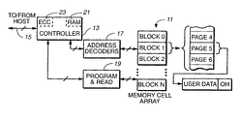
- FIG. 1schematically illustrates an example memory system and operation in which the present invention may be implemented
- FIG. 2is an example, in plan view, of storage elements of memory cells within the array of memory cells of the system of FIG. 1;
- FIGS. 3A and 3Bare curves of programmed memory cell level distributions that illustrate one application of the present invention.
- FIG. 4is a flow chart that provides one example of the operation of the memory system of FIGS. 1 - 3 B;
- FIGS. 5A, 5B and 5 Cillustrate exemplary structures and operation of three types of memory cell arrays in which the present invention may be implemented;
- FIGS. 6A and 6Bshow one technique for programming data into a particular type of existing non-volatile memory cell array
- FIG. 6Cillustrates another programming technique that is carried out as part of the special operation illustrated in FIG. 8;
- FIG. 7illustrates one format of repetitive programming pulses used to program non-volatile memory cells, which may be used with the programming illustrated in FIGS. 6A, 6B and 6 C;
- FIG. 8is a flow chart showing a special operation of the particular type of existing non-volatile memory cell array whose normal data programming is illustrated in FIGS. 6A and 6B.
- FIG. 1a general diagram of the interrelationship of major components of an example mass memory system is shown in FIG. 1.
- a primary component of this systemis a memory 11 , such as an array of memory cells formed on a semiconductor substrate, wherein one or more bits of data are stored in the individual memory cells by storing one of two or more levels of charge on individual storage elements of the memory cells.
- a non-volatile flash EEPROMis a common type of memory for such systems, and is used in this example.
- a second primary component of the memory system of FIG. 1is a controller 13 .
- the controller 13communicates over a bus 15 to a host computer or other system that is using the memory system to store data.
- the controller 13also controls operation of the memory cell array 11 to write data provided by the host, read data requested by the host and perform various housekeeping functions in operating the memory.
- the controller 13normally includes a general purpose microprocessor, with associated non-volatile software memory, various logic circuits, and the like.
- One or more state machinesare often also included for controlling the performance of specific routines.
- the memory cell array 11is addressed by the controller 13 through address decoders 17 .
- the decoders 17apply the correct voltages to gate and bit lines of the array 11 in order to program data to, read data from, or erase a group of memory cells being addressed by the controller 13 .
- Additional circuits 19include programming drivers that control voltages applied to elements of the array that depend upon the data being programmed into an addressed group of cells.
- the circuits 19also include sense amplifiers and other circuits necessary to read data from an addressed group of memory cells.
- Various specific forms of the circuits 17 and 19are described in the patents and patent applications identified in the previous Background section. Data to be programmed into the array, or data recently read from the array, are typically stored in a buffer memory 21 within the controller 13 .
- the controller 13also usually contains various registers for temporarily storing command and status data, and the like.
- the array 11is divided into a large number of BLOCKS 0-N of memory cells.
- the blockis the unit of erase. That is, each block contains the minimum number of memory cells that are erased together.
- Each blockis typically divided into a number of pages, as also illustrated in FIG. 1.
- a pageis the unit of programming. That is, a basic programming operation writes data into a minimum of one page of cells.
- One or more sectors of dataare stored within each page. As shown in FIG. 1, one sector includes user data and overhead data. Overhead data typically includes an ECC that has been calculated from the user data of the sector.
- a portion 23 of the controller 13calculates the ECC when data is being programmed into the array 11 , and also checks it when data is being read from the array 11 .
- the ECCsare stored in different pages, or different blocks, than the user data to which they pertain.
- a sector of user datais typically 512 bytes, corresponding to the size of a sector in magnetic disk drives. Overhead data is typically an additional 28 bytes.
- One sector of datais most commonly included in each page but two or more sectors may instead form a page.
- a large number of pagesform a block, anywhere from 8 pages, for example, up to 512, 1024 or more pages.
- the number of blocksis chosen to provide a desired data storage capacity for the memory system.
- the array 11is typically divided into a few sub-arrays (not shown), each of which contains a proportion of the blocks, which operate somewhat independently of each other in order to increase the degree of parallelism in the execution of various memory operations.
- An example of the use of multiple sub-arraysis described in U.S. Pat. No. 5,890,192, which patent is incorporated herein by this reference.
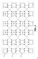
- FIG. 2shows an arrangement of storage elements (squares) in an array of memory cells in order to illustrate the capacitive coupling (dashed lines) between rows of them.
- a storage element 25 of a row 35for example, it is field coupled to storage elements in each of the adjacent rows 37 and 39 .
- the storage element 25is most closely coupled with the storage elements 27 and 31 , because of their proximity, but also have a lesser degree of coupling with storage elements 26 , 28 , 32 and 30 that are further away.
- the amount of coupling between two storage elementsdepends upon the distance between them, the dielectric constant of insulating material between them, whether there are any conductive surfaces between them, and the like.
- FIG. 2illustrates only field coupling between rows of storage elements, such coupling also exists between columns of storage elements. This is not being considered in the examples being described herein because, in these examples, data is programmed into memory cells in units of individual rows, the coupling between the rows has been found to be the cause of the apparent shift in programmed levels. For example, if data are programmed as distinct charge levels on the storage elements of the row 35 , a later change in the charge levels on either or both of the adjacent rows 37 and 39 will cause a shift in the apparent charge levels that are then read from the storage elements of the row 35 .
- the amount of such a shift in the apparent charge level read from a particular storage element of the row 35depends upon the degree of coupling with other storage elements whose charge was later changed in level and the amount of that change.
- the amounts of the shifts that resultare unknown unless the patterns of data programmed into each row are monitored and calculations of their effect made as part of each read operation.
- FIG. 3Ashows an example of the effect upon a first group of memory cells, such as a row of cells, of the later programming of a second group of memory cells, such as an adjacent row of cells.
- a first group of memory cellssuch as a row of cells
- second group of memory cellssuch as an adjacent row of cells.
- four distinct charge levelsare defined for each storage element, thereby to store two bits of data on each storage element. Since the level of charge stored on a storage element changes the threshold voltage (V T ) of its memory cell transistor, the threshold voltage is shown on the horizontal axis of the curves of FIG. 3A.
- the solid linesshow the distributions of the number of threshold voltages of all the cells in a page immediately after being programmed, before any change is made to the adjacent pages.
- the vertical axisis the number of cells at each threshold level, the curves having essentially a Gaussian distribution.
- a curve 45is the distribution of the cells in the erased state, which, in this example, is also designated as a programmed state of the bits 11 . When a block of cells is erased, the cells are reset to the 11 state.
- Each cell of a page being programmed to one of the other programmed states 47 , 49 or 51has electrons injected onto its storage element until its threshold reaches the state corresponding respectively to the data 01, 00 or 01 being programmed into the cell.
- Suitable programming techniquesare described in other patents identified above in the Background. Briefly, cells of a page being programmed are programmed in parallel with chunks of data that are a fraction of the capacity of the page or, if the array and system allow, the entire page. Those being programmed into the 10 state are alternately pulsed with programming voltages and then verified by use of a read threshold level V 10 .
- a verify level V 00is used. If to 01, a verify level V 10 is used.
- the particular data bit pair assigned to each of the distributions 45 , 47 , 49 and 51may be different that shown in FIG. 3A, and may even be rotated during operation of the memory system in order to even out wear on the array.
- One corrective technique used in the pastis to read the page again by simply moving the reading threshold levels R 10 , R 00 and/or R 01 within the margins to avoid the effect of the spreading. Since the spreading can come from both sides of each margin, this requires that the margins be maintained wider than is normally desired in order to prevent the distributions of adjacent states from overlapping. It is thus preferable to take some other action to recover the data, in such a circumstance, that does not require maintaining wide margins between the programmed states.
- the programmed distributionsappear to spread in the manner shown in FIG. 3A when the data subsequently programmed into the adjacent page is random; that is, when the state stored in each storage element can be any of the four possible states.
- a storage element programmed to a level at the lower edge of the distribution 47will be read to have the same level in the distribution 47 ′ if the charge level on adjacent storage elements does not change during the subsequent programming.
- a storage element initially programmed to a level at the upper edge of the distribution 47will, if the adjacent storage elements are subsequently programmed from an erased state 11 to the highest state 01, be read to have a level that is increased by an amount ⁇ .
- the originally programmed pageis then read with thresholds that are also shifted by ⁇ , the same amount that the apparent distributions 45 ′′, 47 ′′, 49 ′′ and 51 ′′ have been shifted from the respective original distributions 45 , 47 , 49 and 51 .
- the new read threshold levelsare R 10 + ⁇ , R 00 + ⁇ and R 01 + ⁇ , as shown on FIG. 3B.
- a first step 55is to read the user data and its stored ECC in a normal manner. This can be, for example, a page formed by the row 37 of memory cells illustrated in FIG. 2.
- the read datais then compared with the ECC, in a step 57 . If there are no errors in the data, as determined by comparison with the ECC, as indicated by the step 59 , the read data is sent to the host, as shown by a step 65 . This is the process that is followed for most all reads. In other cases, where one or more bit errors in the read data are present, the errors may be correctable, as determined by a step 61 . If so, the read data is corrected, in a step 63 , and the corrected data than sent to the host, through step 65 . Almost all of the pages read in a useful system will follow this process.
- a first step 67 of this processis to read the data from that next page. If there are no errors in the data, as determined by steps 69 and 71 , or if there are errors that are correctable, as accomplished by steps 73 and 75 , this read data is stored elsewhere, as indicated by a step 79 .
- the page of datacan be directly written to another page in the memory cell array, or can first be temporarily stored in the controller memory 21 for later writing back into the array.
- the charge levels of the storage elements of that pageare increased to a common level, most conveniently to the maximum threshold level of a normal programming operation. This is indicated by a step 81 .
- Those storage elements within the page 35 that are already at that levelare not further programmed, and the others are subjected to the usual program/verify cycles until each storage element contains the maximum charge (the threshold level 01 is reached). This can be done by the system's normal programming operation but, of course, user data is not being programmed. All memory cell transistors are programmed to the highest 01 state.
- a step 83the page 37 is again read with the higher read threshold levels, as previously explained with respect to FIG. 3B.
- This read datais then subjected to an ECC check, as indicated by the steps 85 , 87 , 89 and 91 . If there are no errors in the data, or if any errors can be corrected, the read data are sent to the host by the step 65 . The data recovery process has then been a success. On the other hand, if the data read by the step 83 has too many errors to be used, then the address of the page that cannot be read is stored, as indicated by the step 93 . The attempted data recovery process is then ended.
- a next step 77is to store the address of the failed page and then return to the step 67 for the next page in physical proximity to the page 37 , the page 39 of FIG. 2 being this page. What this determines is that both of the pages 37 and 35 require the process of to be applied to recover data from them.
- the step 81is then applied to the next page 39 , in proximity to the pages 37 and 35 .
- the data reading steps 83 - 91are then caused to be repeated for the second failed page 35 . If there are more than two failed pages in succession, the process steps through each until valid data is read from a page.
- FIG. 5Aillustrates the sequence in which rows of memory cells are programmed according to one technique that is used in at least one commercial NAND array.
- Each row of an erased blockis programmed in sequence, one after the other, wherein one row includes one or more pages of the memory.
- the details of the data recovery described above with respect to FIGS. 2 - 4apply to this type of memory. Since the order of programming of the rows of the pages are known, the row written after the failed read of a row is known. It is that subsequently written row that is written to the higher state in order to recover data of the failed read row. For example, if valid data cannot be read from the row 101 , it is the cells of the subsequently programmed row 103 that are programmed to their highest states.
- Datais then read from the row 101 , more likely now to be valid data.
- the adjacent row 105 on the other side of the failed read pageneed not be considered since its data were written before that of the row 101 , so the data levels stored in the row 105 have not changed the apparent data levels read from the row 101 .
- rows within a blockare programmed in an order that is independent of their relative positions. For example, a row 105 is first programmed, followed by rows 107 , 109 , 111 , 113 and 115 , in that order. But during a read operation of the pages formed by these rows, the order of their programming may not be known. For example, if data read from the row 107 are not valid and cannot be corrected by the ECC, it may not be known which of the adjacent rows 105 and 109 was later programmed and thus a likely cause of the error in reading the row 107 .
- both adjacent rows 105 and 109are reprogrammed to their highest states before again reading data from the row 107 . If the order is known, of course, only the adjacent row that was later programmed is treated in this way. In this case, the row 109 would be so treated while the row 107 would not.
- the ordercan be known, for example, by maintaining a time stamp or programming order number as part of the overhead data associated with the individual sectors of user data.
- a couple of interesting things about the particular example shown in FIG. 5Bmay be noted. If invalid data is initially read from the row 105 , which was the first to be programmed in the block, the levels of the cells of the rows 107 and 113 on both sides of the row 105 would need to be raised to their highest levels, since they have both been programmed with user data after programming the row 105 . Fields from one or both of the rows 107 and 113 can be causing the invalid read of the row 105 , so they both need to be raised in level. Further, if invalid data is initially read from the row 113 , the fields created from the adjacent rows 105 and 111 are likely not the cause of the error because the row 113 was programmed before either of its adjacent rows. In such a case, the recovery process can be avoided and the data in the row 113 marked as invalid.
- FIG. 5Cillustrates another array architecture in which the data recovery process being described may be implemented.
- This architectureis described in U.S. Pat. No. 5,579,259, which patent is incorporated herein by this reference.
- Memory cells within two adjacent rows 117 and 119form a block, in that the cells of both rows are erased from a common erase gate line 121 .
- the capacity of the blockis one up to many sectors of data but the block is also the unit of programming.
- This structure of a pair of memory cell rows with an intermediate erase gateis repeated across the array.
- the recovery process hereinis applied to an adjacent block that was subsequently programmed, or, if it is not known which adjacent block was programmed later, to both of the blocks adjacent the block from which invalid data has been read, on either side.
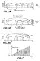
- FIGS. 6A and 6Bdemonstrate an existing programming technique that is employed with a particular NAND system discussed in the Background above, in connection with patents and a patent application there incorporated by reference. They illustrate threshold voltage distributions for the memory cell array when each storage element stores two bits of data, namely four data states, similar to illustration of FIGS. 3A and 3B.
- the curve 125represents a distribution of the threshold levels V T of the cells within the array that are in the erased state (“11” data state), being negative threshold voltage levels.
- Threshold voltage distributions 126 and 127 of memory cells storing “10” and “00” user data, respectively,are between 0 volts and 1 volt and between 1 volts and 2 volts.
- a curve 128the distribution of cells that have been programmed to the “01” data state, being the highest threshold voltage level, set more than 2 volts and less than 4.5 volts.
- Each of the two bits stored in a single memory cellis from a different logical page. That is, each bit of the two bits stored in each memory cell carries a different logical page address from each other. The lower bit shown is accessed when a lower page address is input. The upper bit shown is accessed when an upper page address is input.
- FIGS. 6A and 6Balso illustrate the specific existing technique used to program a 4-state NAND memory cell in an array of the type described above.
- the cell's threshold levelis set according to the bit from the lower logical page. If that bit is a “1”, nothing is done since it is in that state as a result of having been earlier erased. However, if that bit is a “0”, the level of the cell is increased to the first programmed state 126 . That concludes the first programming pass.
- the cell's threshold levelis set according to the bit being stored in the cell from the upper logical page. If a “1”, no programming occurs since the cell is in one of the states 125 or 126 , depending upon the programming of the lower page bit, both of which carry an upper page bit of “1”. If the upper page bit is a “0”, however, the cell is programmed a second time. If the first pass resulted in the cell remaining in the erased state 125 , the cell is programmed from that state to the highest most state 128 , as shown by the upper arrow FIG. 6B.
- the cellis further programmed in the second pass from that state to the state 127 , as shown by the lower arrow of FIG. 6B.
- the result of the second passis to program the cell into the state designated to store a “0” from the upper page without changing the result of the first pass programming.
- a typical programming voltage Vpgm waveformis illustrated in FIG. 7.
- the programming voltage Vpgmis divided into many pulses, and increased 0.2 volt pulse-by-pulse.
- the Vpgm step sizeis 0.2 volt.
- the maximum width of the resulting distributionis thus 0.2 volt.
- the program verify operationsare carried out. That is, the programmed level of each cell being programmed in parallel is read between each programming pulse to determine whether it is equal to or greater than the verify level to which it is being programmed. If it is determined that the threshold voltage of a given memory cell has exceeded the verify level, Vpgm is removed by raising the voltage of the bit line to which the series cell unit of the given cell is connected from 0 volts to Vdd. Programming of others of the cells being programmed in parallel continues until they in turn reach their verify levels.
- the normal programming operationdoes not allow all the cells of a page to be increased to the highest level 128 when the recovery of data from an adjacent page is taking place.
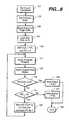
- the threshold level V T of the cellFor a cell in the state 127 , there is no standard programming operation to move the threshold level V T of the cell to the highest state 128 . Therefore, in order to be able to move all cells of any page to the highest level 128 as part of recovering data from an adjacent page, another programming-like operation is added. This additional operation, initiated in response to an “ALL01” command, is shown in the flow chart of FIG. 8.
- the system programming algorithmis set ( 131 ) to execute the ALL01 command, following by an act 133 of setting the address of the page whose memory cells are to have there threshold voltages raised to the 01 programmed state.
- the data stored in the cells of the addressed pageare read ( 135 ), followed by locking out all of those cells that are already in the 01 state ( 137 ). That is, none of the cells of the page in the 01 state are to receive programming voltages.
- a programming voltage Vpgmis set at 14 volts, in this specific example, and a pulse counter (“PC”) is set to 0, as shown at 139 .
- the operationthen follows a loop beginning with the application of one programming or more pulses ( 141 ), followed by reading the states of the cells being programmed ( 143 ). If any cells have reached the 01 state, as indicated by 145 , they are noted to have passed ( 149 ) and further programming of them is locked out. But if some of theses cells are not yet in the 01 state, the process continues to a determination ( 147 ) of whether a certain maximum number of programming pulses, in this case 35, have been applied. If so, it is noted ( 151 ) that the process has failed as to the cells not in the 01 state, and the process is ended ( 153 ).
- FIG. 6Cillustrates this method of programming the memory cells of the addressed page to the highest state 128 . Data in the adjacent page that was first read to be invalid is now read again in order to recover that data, as described above.
Landscapes
- Engineering & Computer Science (AREA)
- Computer Hardware Design (AREA)
- Read Only Memory (AREA)
- For Increasing The Reliability Of Semiconductor Memories (AREA)
- Semiconductor Memories (AREA)
- Dram (AREA)
- Image Processing (AREA)
Abstract
Description
- This invention relates generally to the field of data memories, and, more specifically, to memories of the type that store data as levels of electronic charge, including, but not limited to, flash electrically erasable and programmable read-only-memories (flash EEPROMs) utilizing either conductive floating gates or dielectric material as charge storage elements.[0001]
- It is common in current commercial products for each storage element of a flash EEPROM array to store a single bit of data by operating in a binary mode, where two ranges of threshold levels of the storage element transistors are defined as storage levels. The threshold levels of transistors correspond to ranges of charge levels stored on their storage elements. In addition to shrinking the size of the memory arrays, the trend is to further increase the density of data storage of such memory arrays by storing more than one bit of data in each storage element transistor. This is accomplished by defining more than two threshold levels as storage states for each storage element transistor, four such states (2 bits of data per storage element) now being included in commercial products. More storage states, such as 16 states per storage element, are contemplated. Each storage element memory transistor has a certain total range (window) of threshold voltages in which it may practically be operated, and that range is divided into the number of states defined for it plus margins between the states to allow for them to be clearly differentiated from one another.[0002]
- As the number of states stored in each memory cell increases, the tolerance of any shifts in the programmed charge level on the storage elements decreases. Since the ranges of charge designated for each storage state must necessarily be made narrower and placed closer together as the number of states stored on each memory cell storage element increases, the programming must be performed with an increased degree of precision and the extent of any post-programming shifts in the stored charge levels that can be tolerated, either actual or apparent shifts, is reduced. Actual disturbs to the charge stored in one cell can be created when programming and reading that cell, and when reading, programming and erasing other cells that have some degree of electrical coupling with the that cell, such as those in the same column or row, and those sharing a line or node.[0003]
- Apparent shifts in the stored charge levels occur because of field coupling between storage elements. The degree of this coupling is necessarily increasing as the sizes of memory cell arrays are being decreased, which is occurring as the result of improvements of integrated circuit manufacturing techniques. The problem occurs most pronouncedly between two groups of adjacent cells that have been programmed at different times. One group of cells is programmed to add a level of charge to their storage elements that corresponds to one set of data. After the second group of cells is programmed with a second set of data, the charge levels read from the storage elements of the first group of cells often appear to be different than programmed because of the effect of the charge on the second group of storage elements being capacitively coupled with the first. This is known as the Yupin effect, and is described in U.S. Pat. No. 5,867,429, which patent is incorporated herein in their entirety by this reference. This patent describes either physically isolating the two groups of storage elements from each other, or taking into account the effect of the charge on the second group of storage elements when reading that of the first group.[0004]
- In the types of memory systems described herein, as well as in others, including magnetic disc storage systems, the integrity of the data being stored is maintained by use of an error correction technique. Most commonly, an error correction code (ECC) is calculated for each sector or other unit of data that is being stored at one time, and that ECC is stored along with the data. The ECC is most commonly stored together with the sector of user data from which the ECC has been calculated. When this data is read from the memory, the ECC is used to determine the integrity of the user data being read. One or a few erroneous bits of data within a sector of data can often be corrected by use of the ECC but the existence of more errors renders the attempted data read to fail. Thus, the existence of bits that are read incorrectly because of close field coupling with adjacent memory cells can cause an attempted data read to fail.[0005]
- In order to be able to recover valid data from a failed read of a first group of memory cells, as determined to have failed by the use of an ECC or otherwise, the data in at least an adjacent second group of memory cells, which are field coupled with the first group being read, are read and written elsewhere, either temporarily or permanently, followed by adjusting the programmed levels of the cells in the second group to that which allows the data originally written in the first group of cells to be accurately read. Ideally, the programmed levels of the second group of memory cells are returned to those existing when the first group of cells was programmed with the data that is now being read. The data is then accurately read from the first group since the fields coupled from the second group of cells are then the same as when the first group was programmed. But since it is often not practical to return the second group to the condition that existed when the first group was programmed, either because that initial condition is not known or for other reasons, the programmed levels of the cells of the second group are alternatively adjusted to a common level, usually the highest programmed level of the memory system.[0006]
- The present invention can be implemented in various types of flash EEPROM cell arrays. A NOR array of one design has its memory cells connected between adjacent bit (column) lines and control gates connected to word (row) lines. The individual cells contain either one storage element transistor, with or without a select transistor formed in series with it, or two storage element transistors separated by a single select transistor. Examples of such arrays and their use in storage systems are given in the following U.S. patents and pending applications of SanDisk Corporation that are incorporated herein in their entirety by this reference: U.S. Pat. Nos. 5,095,344, 5,172,338, 5,602,987, 5,663,901, 5,430,859, 5,657,332, 5,712,180, 5,890,192, 6,091,633, 6,103,573 and 6,151,248, and applications Ser. No. 09/505,555, filed Feb. 17, 2000, Ser. No. 09/667,344, filed Sep. 22, 2000, Ser. No. 09/925,102, filed Aug. 8, 2001, and Ser. No. 09/925,134, filed Aug. 8, 2001.[0007]
- A NAND array of one design has a number of memory cells, such as 8, 16 or even 32, connected in a series string between a bit line and a reference potential through select transistors at either end. Word lines are connected with control gates of cells across different series strings. Relevant examples of such arrays and their operation are given in the following U.S. patents and patent application that are incorporated herein in their entirety by this reference: U.S. Pat. Nos. 5,570,315, 5,774,397 and 6,046,935, and application Ser. No. 09/893,277, filed Jun. 27, 2001. Briefly, two bits of data from different logical pages of incoming data are programmed into one of four states of the individual cells in two steps, first programming a cell into one state according to one bit of data and then, if the data makes it necessary, re-programming that cell into another one of its states according to the second bit of incoming data.[0008]
- The above-referenced patents and patent applications describe flash EEPROM systems that use conductive floating gates as memory cell storage elements. Alternatively, flash EEPROM systems with memory cells employing charge trapping dielectric material in place of floating gates are operated in substantially the same way. Examples of this are included in patent application Ser. No. 10/002,696, filed Oct. 31, 2001, by Harari et al., entitled “Multi-State Non-Volatile Integrated Circuit Memory Systems that Employ Dielectric Storage Elements,” which application is incorporated herein by this reference. Field coupling between dielectric storage elements of adjacent memory cells can also affect the accuracy of the data read from such memory systems.[0009]
- Additional aspects, features and advantages of the present invention can be had from the following detailed description of exemplary embodiments thereof, which description should be read along with reference to the accompanying drawings.[0010]
- FIG. 1 schematically illustrates an example memory system and operation in which the present invention may be implemented;[0011]
- FIG. 2 is an example, in plan view, of storage elements of memory cells within the array of memory cells of the system of FIG. 1;[0012]
- FIGS. 3A and 3B are curves of programmed memory cell level distributions that illustrate one application of the present invention;[0013]
- FIG. 4 is a flow chart that provides one example of the operation of the memory system of FIGS.[0014]1-3B;
- FIGS. 5A, 5B and[0015]5C illustrate exemplary structures and operation of three types of memory cell arrays in which the present invention may be implemented;
- FIGS. 6A and 6B show one technique for programming data into a particular type of existing non-volatile memory cell array;[0016]
- FIG. 6C illustrates another programming technique that is carried out as part of the special operation illustrated in FIG. 8;[0017]
- FIG. 7 illustrates one format of repetitive programming pulses used to program non-volatile memory cells, which may be used with the programming illustrated in FIGS. 6A, 6B and[0018]6C; and
- FIG. 8 is a flow chart showing a special operation of the particular type of existing non-volatile memory cell array whose normal data programming is illustrated in FIGS. 6A and 6B.[0019]
- In order to explain the present invention and example implementations, a general diagram of the interrelationship of major components of an example mass memory system is shown in FIG. 1. A primary component of this system is a[0020]
memory 11, such as an array of memory cells formed on a semiconductor substrate, wherein one or more bits of data are stored in the individual memory cells by storing one of two or more levels of charge on individual storage elements of the memory cells. A non-volatile flash EEPROM is a common type of memory for such systems, and is used in this example. - A second primary component of the memory system of FIG. 1 is a[0021]
controller 13. Thecontroller 13 communicates over abus 15 to a host computer or other system that is using the memory system to store data. Thecontroller 13 also controls operation of thememory cell array 11 to write data provided by the host, read data requested by the host and perform various housekeeping functions in operating the memory. Thecontroller 13 normally includes a general purpose microprocessor, with associated non-volatile software memory, various logic circuits, and the like. One or more state machines are often also included for controlling the performance of specific routines. - The[0022]
memory cell array 11 is addressed by thecontroller 13 throughaddress decoders 17. Thedecoders 17 apply the correct voltages to gate and bit lines of thearray 11 in order to program data to, read data from, or erase a group of memory cells being addressed by thecontroller 13.Additional circuits 19 include programming drivers that control voltages applied to elements of the array that depend upon the data being programmed into an addressed group of cells. Thecircuits 19 also include sense amplifiers and other circuits necessary to read data from an addressed group of memory cells. Various specific forms of thecircuits buffer memory 21 within thecontroller 13. Thecontroller 13 also usually contains various registers for temporarily storing command and status data, and the like. - The[0023]
array 11 is divided into a large number of BLOCKS 0-N of memory cells. As is common for flash EEPROM systems, the block is the unit of erase. That is, each block contains the minimum number of memory cells that are erased together. Each block is typically divided into a number of pages, as also illustrated in FIG. 1. A page is the unit of programming. That is, a basic programming operation writes data into a minimum of one page of cells. One or more sectors of data are stored within each page. As shown in FIG. 1, one sector includes user data and overhead data. Overhead data typically includes an ECC that has been calculated from the user data of the sector. Aportion 23 of thecontroller 13 calculates the ECC when data is being programmed into thearray 11, and also checks it when data is being read from thearray 11. Alternatively, the ECCs are stored in different pages, or different blocks, than the user data to which they pertain. - A sector of user data is typically 512 bytes, corresponding to the size of a sector in magnetic disk drives. Overhead data is typically an additional 28 bytes. One sector of data is most commonly included in each page but two or more sectors may instead form a page. A large number of pages form a block, anywhere from 8 pages, for example, up to 512, 1024 or more pages. The number of blocks is chosen to provide a desired data storage capacity for the memory system. The[0024]
array 11 is typically divided into a few sub-arrays (not shown), each of which contains a proportion of the blocks, which operate somewhat independently of each other in order to increase the degree of parallelism in the execution of various memory operations. An example of the use of multiple sub-arrays is described in U.S. Pat. No. 5,890,192, which patent is incorporated herein by this reference. - FIG. 2 shows an arrangement of storage elements (squares) in an array of memory cells in order to illustrate the capacitive coupling (dashed lines) between rows of them. Considering a[0025]
storage element 25 of arow 35, for example, it is field coupled to storage elements in each of theadjacent rows storage element 25 is most closely coupled with thestorage elements storage elements - Although FIG. 2 illustrates only field coupling between rows of storage elements, such coupling also exists between columns of storage elements. This is not being considered in the examples being described herein because, in these examples, data is programmed into memory cells in units of individual rows, the coupling between the rows has been found to be the cause of the apparent shift in programmed levels. For example, if data are programmed as distinct charge levels on the storage elements of the[0026]
row 35, a later change in the charge levels on either or both of theadjacent rows row 35. The amount of such a shift in the apparent charge level read from a particular storage element of therow 35 depends upon the degree of coupling with other storage elements whose charge was later changed in level and the amount of that change. When the later change is caused by programming data into the adjacent row, the amounts of the shifts that result are unknown unless the patterns of data programmed into each row are monitored and calculations of their effect made as part of each read operation. - FIG. 3A shows an example of the effect upon a first group of memory cells, such as a row of cells, of the later programming of a second group of memory cells, such as an adjacent row of cells. In this example, four distinct charge levels are defined for each storage element, thereby to store two bits of data on each storage element. Since the level of charge stored on a storage element changes the threshold voltage (V[0027]T) of its memory cell transistor, the threshold voltage is shown on the horizontal axis of the curves of FIG. 3A. The solid lines show the distributions of the number of threshold voltages of all the cells in a page immediately after being programmed, before any change is made to the adjacent pages. The vertical axis is the number of cells at each threshold level, the curves having essentially a Gaussian distribution. A
curve 45 is the distribution of the cells in the erased state, which, in this example, is also designated as a programmed state of thebits 11. When a block of cells is erased, the cells are reset to the11 state. - Each cell of a page being programmed to one of the other[0028]
programmed states data distributions - It is desired to maintain a sufficient margin between the[0029]
states - The spreading of the distributions that occurs as the result of subsequently programming an adjacent row of cells is shown in dashed lines in FIG. 3A. Even when significant margins are maintained during the initial programming of a row of cells, these margins can be significantly narrowed when the distributions spread as a result of later programming an adjacent row of cells. If just a few of the cells spread from below to above one of the reading thresholds R[0030]10, R00and/or R01, there can be enough erroneous readings to overwhelm an ECC. In such a case, the data cannot be read with those thresholds, so are designated as invalid unless some corrective action is taken. One corrective technique used in the past is to read the page again by simply moving the reading threshold levels R10, R00and/or R01within the margins to avoid the effect of the spreading. Since the spreading can come from both sides of each margin, this requires that the margins be maintained wider than is normally desired in order to prevent the distributions of adjacent states from overlapping. It is thus preferable to take some other action to recover the data, in such a circumstance, that does not require maintaining wide margins between the programmed states.
- The programmed distributions appear to spread in the manner shown in FIG. 3A when the data subsequently programmed into the adjacent page is random; that is, when the state stored in each storage element can be any of the four possible states. A storage element programmed to a level at the lower edge of the[0031]
distribution 47, for example, will be read to have the same level in thedistribution 47′ if the charge level on adjacent storage elements does not change during the subsequent programming. On the other hand, a storage element initially programmed to a level at the upper edge of thedistribution 47 will, if the adjacent storage elements are subsequently programmed from an erasedstate 11 to thehighest state 01, be read to have a level that is increased by an amount Δ. The higher charge levels on the adjacent storage elements are coupled with the previously programmed storage element whose level is being read. Other combinations of initial and later programming of adjacent cells of thedistribution 47 fall between these two extremes, thereby resulting in theapparent distribution 47′. The lower end of theapparent distribution 47′ remains at the same level but its spread is increased by Δ. - If the data read from the initial row is invalid, a heroic process takes place to recover the data. The system is designed to have sufficient margins so that this does not occur very often but, at the same time, to provide a technique to handle it when necessary, thus avoiding the need to make the margins so wide that this condition never occurs. The recovery process involves changing the charge levels on the later programmed page. If the memory array is of a type having only one page per block, the subsequently programmed block can be erased (after reading its data and writing it in another location, of course). This returns the adjacent page of cells to their condition when the problematic page was initially programmed. That initial page will then exhibit the[0032]
original distributions - However, most flash EEPROM systems are of the type illustrated in FIG. 1, where a block contains a large number of pages. The later programmed page cannot then be erased without erasing all other pages of the block. Therefore, in such a case, charge is added to the storage elements of the later written page that are not already in the highest state by further programming until they are all in the highest threshold state. The result on the originally programmed page is shown in FIG. 3B, where the apparent distributions are tightened. The upper end of the[0033]
distribution 47″, for example, remains the same as that of thedistribution 47′ of FIG. 3A, while the lower end is moved upward by approximately Δ. Every storage element of the originally programmed page is pulled up by the influence of the high charge level of the storage elements of the other page. The originally programmed page is then read with thresholds that are also shifted by Δ, the same amount that theapparent distributions 45″,47″,49″ and51″ have been shifted from the respectiveoriginal distributions - The reading process for a page of data is outlined by the flow chart of FIG. 4. A[0034]
first step 55 is to read the user data and its stored ECC in a normal manner. This can be, for example, a page formed by therow 37 of memory cells illustrated in FIG. 2. The read data is then compared with the ECC, in astep 57. If there are no errors in the data, as determined by comparison with the ECC, as indicated by thestep 59, the read data is sent to the host, as shown by astep 65. This is the process that is followed for most all reads. In other cases, where one or more bit errors in the read data are present, the errors may be correctable, as determined by astep 61. If so, the read data is corrected, in astep 63, and the corrected data than sent to the host, throughstep 65. Almost all of the pages read in a useful system will follow this process. - But for the rare occasion where the data is determined by the[0035]
step 61 to not be correctable, the extra steps described above are taken. The charge levels of a next adjacent page, such as the page formed by therow 35 of FIG. 2, are then adjusted to the highest programmed level. Afirst step 67 of this process is to read the data from that next page. If there are no errors in the data, as determined bysteps steps step 79. The page of data can be directly written to another page in the memory cell array, or can first be temporarily stored in thecontroller memory 21 for later writing back into the array. After a copy of the data of thepage 35 is safely stored somewhere, the charge levels of the storage elements of that page are increased to a common level, most conveniently to the maximum threshold level of a normal programming operation. This is indicated by astep 81. Those storage elements within thepage 35 that are already at that level are not further programmed, and the others are subjected to the usual program/verify cycles until each storage element contains the maximum charge (thethreshold level 01 is reached). This can be done by the system's normal programming operation but, of course, user data is not being programmed. All memory cell transistors are programmed to the highest01 state. - Thereafter, as indicated by a[0036]
step 83, thepage 37 is again read with the higher read threshold levels, as previously explained with respect to FIG. 3B. This read data is then subjected to an ECC check, as indicated by thesteps step 65. The data recovery process has then been a success. On the other hand, if the data read by thestep 83 has too many errors to be used, then the address of the page that cannot be read is stored, as indicated by thestep 93. The attempted data recovery process is then ended. Unless there is some other alternate technique that is available for trying to recover the data, that page of data cannot be returned to the host. The system and this recovery process are designed, however, for such an absolute failure to seldom, if ever, result from the field coupling between adjacent pages of the memory array. - If, at[0037]
step 73, it is determined that the data read from thenext page 35 is not free of errors and is not correctable, anext step 77 is to store the address of the failed page and then return to thestep 67 for the next page in physical proximity to thepage 37, thepage 39 of FIG. 2 being this page. What this determines is that both of thepages step 81 is then applied to thenext page 39, in proximity to thepages step 95, the data reading steps83-91 are then caused to be repeated for the second failedpage 35. If there are more than two failed pages in succession, the process steps through each until valid data is read from a page. - FIG. 5A illustrates the sequence in which rows of memory cells are programmed according to one technique that is used in at least one commercial NAND array. Each row of an erased block is programmed in sequence, one after the other, wherein one row includes one or more pages of the memory. The details of the data recovery described above with respect to FIGS.[0038]2-4 apply to this type of memory. Since the order of programming of the rows of the pages are known, the row written after the failed read of a row is known. It is that subsequently written row that is written to the higher state in order to recover data of the failed read row. For example, if valid data cannot be read from the
row 101, it is the cells of the subsequently programmedrow 103 that are programmed to their highest states. Data is then read from therow 101, more likely now to be valid data. Theadjacent row 105 on the other side of the failed read page need not be considered since its data were written before that of therow 101, so the data levels stored in therow 105 have not changed the apparent data levels read from therow 101. - In other types of memory systems, however, this order of programming rows is not a constraint. Referring to FIG. 5B, for example, it is shown that rows within a block are programmed in an order that is independent of their relative positions. For example, a[0039]
row 105 is first programmed, followed byrows row 107 are not valid and cannot be corrected by the ECC, it may not be known which of theadjacent rows row 107. If this is not known, bothadjacent rows row 107. If the order is known, of course, only the adjacent row that was later programmed is treated in this way. In this case, therow 109 would be so treated while therow 107 would not. The order can be known, for example, by maintaining a time stamp or programming order number as part of the overhead data associated with the individual sectors of user data. - A couple of interesting things about the particular example shown in FIG. 5B may be noted. If invalid data is initially read from the[0040]
row 105, which was the first to be programmed in the block, the levels of the cells of therows row 105 would need to be raised to their highest levels, since they have both been programmed with user data after programming therow 105. Fields from one or both of therows row 105, so they both need to be raised in level. Further, if invalid data is initially read from therow 113, the fields created from theadjacent rows row 113 was programmed before either of its adjacent rows. In such a case, the recovery process can be avoided and the data in therow 113 marked as invalid. - FIG. 5C illustrates another array architecture in which the data recovery process being described may be implemented. One specific example of this architecture is described in U.S. Pat. No. 5,579,259, which patent is incorporated herein by this reference. Memory cells within two[0041]
adjacent rows gate line 121. The capacity of the block is one up to many sectors of data but the block is also the unit of programming. This structure of a pair of memory cell rows with an intermediate erase gate is repeated across the array. When invalid data is read from one such block, the recovery process herein is applied to an adjacent block that was subsequently programmed, or, if it is not known which adjacent block was programmed later, to both of the blocks adjacent the block from which invalid data has been read, on either side. - FIGS. 6A and 6B demonstrate an existing programming technique that is employed with a particular NAND system discussed in the Background above, in connection with patents and a patent application there incorporated by reference. They illustrate threshold voltage distributions for the memory cell array when each storage element stores two bits of data, namely four data states, similar to illustration of FIGS. 3A and 3B. The[0042]
curve 125 represents a distribution of the threshold levels VTof the cells within the array that are in the erased state (“11” data state), being negative threshold voltage levels.Threshold voltage distributions curve 128 the distribution of cells that have been programmed to the “01” data state, being the highest threshold voltage level, set more than 2 volts and less than 4.5 volts. - Each of the two bits stored in a single memory cell, in this example, is from a different logical page. That is, each bit of the two bits stored in each memory cell carries a different logical page address from each other. The lower bit shown is accessed when a lower page address is input. The upper bit shown is accessed when an upper page address is input.[0043]
- FIGS. 6A and 6B also illustrate the specific existing technique used to program a 4-state NAND memory cell in an array of the type described above. In a first programming pass, the cell's threshold level is set according to the bit from the lower logical page. If that bit is a “1”, nothing is done since it is in that state as a result of having been earlier erased. However, if that bit is a “0”, the level of the cell is increased to the first[0044]
programmed state 126. That concludes the first programming pass. - In a second programming pass, the cell's threshold level is set according to the bit being stored in the cell from the upper logical page. If a “1”, no programming occurs since the cell is in one of the[0045]
states state 125, the cell is programmed from that state to the highestmost state 128, as shown by the upper arrow FIG. 6B. If the cell has been programmed into thestate 126, however, as a result of the first programming pass, the cell is further programmed in the second pass from that state to thestate 127, as shown by the lower arrow of FIG. 6B. The result of the second pass is to program the cell into the state designated to store a “0” from the upper page without changing the result of the first pass programming. - Of course, if the memory is operated with more than four states, there will be a number of distributions within the defined voltage threshold window of the memory cells that is equal to the number of states. Further, although specific bit patterns have been assigned to each of the distributions, different bit patterns may be so assigned, in which case the states between which programming occurs can be different than those shown in FIGS. 6A and 6B. A few such variations are discussed in the patents previously referenced in the Background.[0046]
- A typical programming voltage Vpgm waveform is illustrated in FIG. 7. The programming voltage Vpgm is divided into many pulses, and increased 0.2 volt pulse-by-pulse. The Vpgm step size is 0.2 volt. The maximum width of the resulting distribution is thus 0.2 volt.[0047]
- In periods between the pluses, the program verify operations are carried out. That is, the programmed level of each cell being programmed in parallel is read between each programming pulse to determine whether it is equal to or greater than the verify level to which it is being programmed. If it is determined that the threshold voltage of a given memory cell has exceeded the verify level, Vpgm is removed by raising the voltage of the bit line to which the series cell unit of the given cell is connected from 0 volts to Vdd. Programming of others of the cells being programmed in parallel continues until they in turn reach their verify levels.[0048]
- With the specific NAND system operation described with respect to FIGS. 6A, 6B and[0049]7, the normal programming operation does not allow all the cells of a page to be increased to the
highest level 128 when the recovery of data from an adjacent page is taking place. For a cell in thestate 127, there is no standard programming operation to move the threshold level VTof the cell to thehighest state 128. Therefore, in order to be able to move all cells of any page to thehighest level 128 as part of recovering data from an adjacent page, another programming-like operation is added. This additional operation, initiated in response to an “ALL01” command, is shown in the flow chart of FIG. 8. - First, the system programming algorithm is set ([0050]131) to execute the ALL01 command, following by an
act 133 of setting the address of the page whose memory cells are to have there threshold voltages raised to the 01 programmed state. Next, the data stored in the cells of the addressed page are read (135), followed by locking out all of those cells that are already in the 01 state (137). That is, none of the cells of the page in the 01 state are to receive programming voltages. For the remaining cells that are in other than the highest 01state 128, a programming voltage Vpgm is set at 14 volts, in this specific example, and a pulse counter (“PC”) is set to 0, as shown at139. - The operation then follows a loop beginning with the application of one programming or more pulses ([0051]141), followed by reading the states of the cells being programmed (143). If any cells have reached the 01 state, as indicated by145, they are noted to have passed (149) and further programming of them is locked out. But if some of theses cells are not yet in the 01 state, the process continues to a determination (147) of whether a certain maximum number of programming pulses, in this
case 35, have been applied. If so, it is noted (151) that the process has failed as to the cells not in the 01 state, and the process is ended (153). If fewer than 35 programming pulses have been applied, however, the programming voltage Vpgm is increased by 0.2 volt and the pulse counter incremented by one (155). The programming cycle of acts141-155 is then repeated. In the usual case, the process ends (153) when all the cells of the page have been programmed to the 01 state. FIG. 6C illustrates this method of programming the memory cells of the addressed page to thehighest state 128. Data in the adjacent page that was first read to be invalid is now read again in order to recover that data, as described above. - Although the present invention has been described with respect to exemplary embodiments, it will be understood that the invention is entitled to protection within the full scope of the appended claims.[0052]
Claims (23)
1. A method of reading multiple bits of data stored as different ones of a plurality of levels of charge in storage elements of individual memory cells of a first group, wherein the data read is corrupted by other data stored as different ones of the plurality of levels of charge in storage elements of adjacent memory cells of a second group to which the storage elements of the cells of the first group are field coupled, comprising:
reading the charge levels stored in the storage elements of the second group of memory cells, thereby to read the data stored in the second group of memory cells,
storing the data read from the storage elements of the second group of memory cells in a location outside of the first or second group of memory cells,
thereafter altering the levels of charge stored in the individual storage elements of the memory cells of the second group, thereby to alter apparent levels of charge read from the storage elements of the first group of memory cells, and
thereafter reading the charge levels stored in the storage elements of the first group of memory cells, thereby to read the data stored in the storage elements of the first group of memory cells with altered charge levels stored in the storage elements of the second group of cells.
2. The method ofclaim 1 , wherein altering the levels of charge stored in the storage elements of the individual memory cells of the second group includes setting the levels of charge stored in the individual storage elements of the memory cells of the second group to a common level of charge.
3. The method ofclaim 2 , wherein said common level of charge is the highest of the plurality of levels of charge by which data is stored the storage elements of the memory cells of the first group.
4. The method ofclaim 3 , wherein the plurality of levels of charge stored in the individual storage elements of the memory cells is greater than two levels of charge, thereby to store more than one bit of data in the individual storage elements.
5. The method ofclaim 1 , wherein the plurality of levels of charge stored in the individual storage elements of the memory cells is exactly two levels of charge, thereby to store exactly one bit of data in the individual storage elements.
6. The method ofclaim 1 , wherein charge levels are initially stored in the storage elements of the first group and then the second group, in sequence.
7. The method ofclaim 6 , wherein the method is practiced on the first and second groups of memory cells as part of a NAND array of memory cells.
8. The method ofclaim 1 , wherein the method is practiced on the first and second groups of memory cells as part of a NOR array of memory cells having a single storage element per memory cell.
9. The method ofclaim 1 , wherein the method is practiced on the first and second groups of memory cells as part of a NOR array of memory cells having two storage elements per memory cell.
10. The method ofclaim 1 , wherein the first and second groups of memory cells are part of an array of non-volatile memory cells wherein the storage elements are conductive floating gates.
11. The method ofclaim 1 , wherein the first and second groups of memory cells are part of an array of non-volatile memory cells wherein the storage elements are defined areas of a dielectric.
12. A method of reading data stored as different ones of a plurality of levels of charge in individual storage elements of memory cells in an array of memory cells that includes at least first and second groups of memory cells having charge levels of their storage elements field coupled with each other, comprising:
reading the charge levels stored in the storage elements of a first group of memory cells with use of a first set of reference levels, thereby to provide a reading of the data stored in the storage elements of the first group of memory cells,
determining whether or not the data read from the storage elements of the first group of memory cells are valid,
if the data read from the storage elements of the first group of memory cells is determined not to be valid, reading the charge levels stored in the storage elements of the second group of memory cells, thereby to provide a reading of the data stored in the second group of memory cells,
storing the data read from the second group of memory cells,
thereafter altering the levels of charge stored in the individual storage elements of the memory cells of the second group, thereby to alter apparent levels of charge stored in the storage elements of the first group of memory cells due to the field coupling therebetween, and
thereafter reading the charge levels stored in the storage elements of the first group of memory cells with use of a second set of reference levels different from the first set of reference levels, thereby to provide a reading of the data stored in the first group of memory cells that is compensated for the effects of the field coupling between the storage elements of the first and second groups of memory cells.
13. The method ofclaim 12 , wherein altering the levels of charge stored in the individual storage elements of the memory cells of the second group includes setting the levels of charge stored in the individual storage elements of the memory cells of the second group to a common level that is at least as high as the highest of the plurality of levels of charge by which data is stored in the storage elements of the memory cells of the first group.
14. The method ofclaim 13 , wherein the second set of reference levels are higher than the first set of reference levels.
15. The method ofclaim 14 , wherein the plurality of levels of charge stored in the individual storage elements of the memory cells is greater than two levels of charge, thereby to store more than one bit of data in the individual storage elements.
16. The method ofclaim 12 , wherein determining whether or not the data read from the storage elements of the first group of memory cells are valid includes using an error correction code stored when programming the data of the first group of memory cells.
17. The method ofclaim 16 , wherein the plurality of levels of charge stored in the individual storage elements of the memory cells is greater than two levels of charge, thereby to store more than one bit of data in the individual storage elements.
18. The method ofclaim 12 , wherein the plurality of levels of charge stored in the individual storage elements of the memory cells is greater than two levels of charge, thereby to store more than one bit of data in the individual storage elements.
19. The method ofclaim 18 , wherein the memory cells in the array of memory cells are flash EEPROM cells.
20. The method ofclaim 12 , wherein the method is practiced in an array of memory cells wherein the first and second groups of cells include respective first and second adjacent rows of cells.
21. In a flash non-volatile memory system including an array of memory cells connected in NAND strings to form columns and having word lines extending across the columns over rows of cells, wherein adjacent rows are capacitively coupled with each other and programmed in a fixed sequence by increasing the charge levels stored in the individual cells to one of four or more charge levels in a first programming step and to one of at least the highest two or more charge levels in a second programming step, a method of reconstructing data stored in a first row that is read as invalid on account of data subsequently stored in an adjacent second row, comprising:
reading the charge levels stored in the cells of the second row and writing the data represented thereby to another location within the memory system,
thereafter increasing the charge levels of the individual cells of the second row from their programmed levels to the highest programming charge level, and
thereafter reading the charge levels stored in the cells of the first row.
22. The method ofclaim 21 , wherein the method is practiced in a memory system whose memory cells store the charge levels in conductive floating gates.
23. The method ofclaim 21 , wherein the method is practiced in a memory system whose memory cells store the charge levels in a dielectric.
Priority Applications (2)
| Application Number | Priority Date | Filing Date | Title |
|---|---|---|---|
| US10/357,840US6847553B2 (en) | 2002-01-18 | 2003-02-03 | Techniques of recovering data from memory cells affected by field coupling with adjacent memory cells |
| US11/028,906US7102924B2 (en) | 2002-01-18 | 2005-01-03 | Techniques of recovering data from memory cells affected by field coupling with adjacent memory cells |
Applications Claiming Priority (2)
| Application Number | Priority Date | Filing Date | Title |
|---|---|---|---|
| US10/052,759US6542407B1 (en) | 2002-01-18 | 2002-01-18 | Techniques of recovering data from memory cells affected by field coupling with adjacent memory cells |
| US10/357,840US6847553B2 (en) | 2002-01-18 | 2003-02-03 | Techniques of recovering data from memory cells affected by field coupling with adjacent memory cells |
Related Parent Applications (1)
| Application Number | Title | Priority Date | Filing Date |
|---|---|---|---|
| US10/052,759ContinuationUS6542407B1 (en) | 2002-01-18 | 2002-01-18 | Techniques of recovering data from memory cells affected by field coupling with adjacent memory cells |
Related Child Applications (1)
| Application Number | Title | Priority Date | Filing Date |
|---|---|---|---|
| US11/028,906ContinuationUS7102924B2 (en) | 2002-01-18 | 2005-01-03 | Techniques of recovering data from memory cells affected by field coupling with adjacent memory cells |
Publications (2)
| Publication Number | Publication Date |
|---|---|
| US20030137888A1true US20030137888A1 (en) | 2003-07-24 |
| US6847553B2 US6847553B2 (en) | 2005-01-25 |
Family
ID=21979721
Family Applications (3)
| Application Number | Title | Priority Date | Filing Date |
|---|---|---|---|
| US10/052,759Expired - LifetimeUS6542407B1 (en) | 2002-01-18 | 2002-01-18 | Techniques of recovering data from memory cells affected by field coupling with adjacent memory cells |
| US10/357,840Expired - LifetimeUS6847553B2 (en) | 2002-01-18 | 2003-02-03 | Techniques of recovering data from memory cells affected by field coupling with adjacent memory cells |
| US11/028,906Expired - LifetimeUS7102924B2 (en) | 2002-01-18 | 2005-01-03 | Techniques of recovering data from memory cells affected by field coupling with adjacent memory cells |
Family Applications Before (1)
| Application Number | Title | Priority Date | Filing Date |
|---|---|---|---|
| US10/052,759Expired - LifetimeUS6542407B1 (en) | 2002-01-18 | 2002-01-18 | Techniques of recovering data from memory cells affected by field coupling with adjacent memory cells |
Family Applications After (1)
| Application Number | Title | Priority Date | Filing Date |
|---|---|---|---|
| US11/028,906Expired - LifetimeUS7102924B2 (en) | 2002-01-18 | 2005-01-03 | Techniques of recovering data from memory cells affected by field coupling with adjacent memory cells |
Country Status (6)
| Country | Link |
|---|---|
| US (3) | US6542407B1 (en) |
| EP (1) | EP1329898B1 (en) |
| JP (1) | JP4310114B2 (en) |
| KR (1) | KR100904752B1 (en) |
| AT (1) | ATE397273T1 (en) |
| DE (1) | DE60321252D1 (en) |
Cited By (45)
| Publication number | Priority date | Publication date | Assignee | Title |
|---|---|---|---|---|
| US20040268063A1 (en)* | 2003-06-30 | 2004-12-30 | M-Systems Flash Disk Pioneers, Ltd. | Flash memory management method that is resistant to data corruption by power loss |
| US20050018488A1 (en)* | 2003-07-11 | 2005-01-27 | Dong-Hwan Kim | Flash memory device having multi-level cell and reading and programming method thereof |
| US20050219896A1 (en)* | 2004-04-06 | 2005-10-06 | Jian Chen | Variable programming of non-volatile memory |
| US6996004B1 (en)* | 2003-11-04 | 2006-02-07 | Advanced Micro Devices, Inc. | Minimization of FG-FG coupling in flash memory |
| US20060126394A1 (en)* | 2004-12-14 | 2006-06-15 | Yan Li | Multi-state memory having data recovery after program fail |
| US20060221692A1 (en)* | 2005-04-05 | 2006-10-05 | Jian Chen | Compensating for coupling during read operations on non-volatile memory |
| WO2006107651A1 (en)* | 2005-04-01 | 2006-10-12 | Sandisk Corporation | Multi-state memory having data recovery after program fail |
| US7158421B2 (en) | 2005-04-01 | 2007-01-02 | Sandisk Corporation | Use of data latches in multi-phase programming of non-volatile memories |
| US7206230B2 (en) | 2005-04-01 | 2007-04-17 | Sandisk Corporation | Use of data latches in cache operations of non-volatile memories |
| US20070103987A1 (en)* | 2005-04-05 | 2007-05-10 | Yan Li | Read operation for non-volatile storage that includes compensation for coupling |
| US20070140006A1 (en)* | 2005-04-05 | 2007-06-21 | Jian Chen | Compensating for coupling in non-volatile storage |
| US20070153583A1 (en)* | 2005-12-29 | 2007-07-05 | Guterman Daniel C | Alternate row-based reading and writing for non-volatile memory |
| US20070153577A1 (en)* | 2005-12-29 | 2007-07-05 | Guterman Daniel C | Systems for alternate row-based reading and writing for non-volatile memory |
| US20070159885A1 (en)* | 2004-12-30 | 2007-07-12 | Gorobets Sergey A | On-Chip Data Grouping and Alignment |
| US20070206421A1 (en)* | 2006-03-03 | 2007-09-06 | Nima Mokhlesi | Read operation for non-volatile storage with compensation for coupling |
| US20070206426A1 (en)* | 2006-03-03 | 2007-09-06 | Nima Mokhlesi | System for performing read operation on non-volatile storage with compensation for coupling |
| US7301805B2 (en) | 2004-12-14 | 2007-11-27 | Sandisk Corporation | Pipelined programming of non-volatile memories using early data |
| US20070279995A1 (en)* | 2006-06-02 | 2007-12-06 | Nima Mokhlesi | System for performing data pattern sensitivity compensation using different voltage |
| US20070279994A1 (en)* | 2006-06-02 | 2007-12-06 | Nima Mokhlesi | Data pattern sensitivity compensation using different voltage |
| US20070291546A1 (en)* | 2006-06-19 | 2007-12-20 | Teruhiko Kamei | Systems for Programming Differently Sized Margins and Sensing with Compensations at Select States for Improved Read Operations in Non-Volatile Memory |
| US20070291556A1 (en)* | 2006-06-19 | 2007-12-20 | Teruhiko Kamei | Programming Differently Sized Margins and Sensing with Compensations at Select States for Improved Read Operations in Non-Volatile Memory |
| US20080002464A1 (en)* | 2004-12-09 | 2008-01-03 | Eduardo Maayan | Non-volatile memory device and method for reading cells |
| US20080084754A1 (en)* | 2006-09-29 | 2008-04-10 | Nima Mokhlesi | Reverse reading in non-volatile memory with compensation for coupling |
| US20080084755A1 (en)* | 2006-09-29 | 2008-04-10 | Nima Mokhlesi | Systems for reverse reading in non-volatile memory with compensation for coupling |
| US20080158985A1 (en)* | 2006-12-29 | 2008-07-03 | Nima Mokhlesi | Systems for margined neighbor reading for non-volatile memory read operations including coupling compensation |
| US20080158967A1 (en)* | 2006-12-29 | 2008-07-03 | Nima Mokhlesi | Resistance sensing and compensation for non-volatile storage |
| US20080158946A1 (en)* | 2006-12-29 | 2008-07-03 | Nima Mokhlesi | Alternating read mode |
| US20080158973A1 (en)* | 2006-12-28 | 2008-07-03 | Man Lung Mui | Complete word line look ahead with efficient data latch assignment in non-volatile memory read operations |
| US20080158949A1 (en)* | 2006-12-28 | 2008-07-03 | Man Lung Mui | Systems for complete word line look ahead with efficient data latch assignment in non-volatile memory read operations |
| US20080158983A1 (en)* | 2006-12-29 | 2008-07-03 | Nima Mokhlesi | Non-volatile storage system with resistance sensing and compensation |
| US20080158974A1 (en)* | 2006-12-29 | 2008-07-03 | Nima Mokhlesi | Apparatus with alternating read mode |
| US7426137B2 (en) | 2006-04-12 | 2008-09-16 | Sandisk Corporation | Apparatus for reducing the impact of program disturb during read |
| US7436713B2 (en) | 2006-04-12 | 2008-10-14 | Sandisk Corporation | Reducing the impact of program disturb |
| US7440331B2 (en) | 2006-06-01 | 2008-10-21 | Sandisk Corporation | Verify operation for non-volatile storage using different voltages |
| US20080273388A1 (en)* | 2007-03-21 | 2008-11-06 | Henry Chin | Adjusting resistance of non-volatile memory using dummy memory cells |
| US7457163B2 (en) | 2006-06-01 | 2008-11-25 | Sandisk Corporation | System for verifying non-volatile storage using different voltages |
| US7499326B2 (en) | 2006-04-12 | 2009-03-03 | Sandisk Corporation | Apparatus for reducing the impact of program disturb |
| US7515463B2 (en) | 2006-04-12 | 2009-04-07 | Sandisk Corporation | Reducing the impact of program disturb during read |
| US7518923B2 (en) | 2006-12-29 | 2009-04-14 | Sandisk Corporation | Margined neighbor reading for non-volatile memory read operations including coupling compensation |
| US20090125785A1 (en)* | 2004-05-13 | 2009-05-14 | Sergey Anatolievich Gorobets | Pipelined Data Relocation and Improved Chip Architectures |
| US20090310413A1 (en)* | 2008-06-16 | 2009-12-17 | Sandisk Il Ltd. | Reverse order page writing in flash memories |
| US20130047045A1 (en)* | 2011-08-19 | 2013-02-21 | Stec, Inc. | Error indicator from ecc decoder |
| US8472280B2 (en) | 2010-12-21 | 2013-06-25 | Sandisk Technologies Inc. | Alternate page by page programming scheme |
| WO2013096830A1 (en)* | 2011-12-22 | 2013-06-27 | Micron Technology, Inc. | Apparatus and methods of programming memory cells using adjustable charge state level(s) |
| US8914703B2 (en) | 2004-12-21 | 2014-12-16 | SanDisk Technologies, Inc. | Method for copying data in reprogrammable non-volatile memory |
Families Citing this family (239)
| Publication number | Priority date | Publication date | Assignee | Title |
|---|---|---|---|---|
| JP5019681B2 (en) | 2001-04-26 | 2012-09-05 | ルネサスエレクトロニクス株式会社 | Thin film magnetic memory device |
| US7108975B2 (en)* | 2001-09-21 | 2006-09-19 | Regents Of The University Of Michigan | Atlastin |
| JP2003134414A (en)* | 2001-10-22 | 2003-05-09 | Pioneer Electronic Corp | Processor, method, and program for video processing |
| US6542407B1 (en)* | 2002-01-18 | 2003-04-01 | Sandisk Corporation | Techniques of recovering data from memory cells affected by field coupling with adjacent memory cells |
| US6781877B2 (en)* | 2002-09-06 | 2004-08-24 | Sandisk Corporation | Techniques for reducing effects of coupling between storage elements of adjacent rows of memory cells |
| US6829167B2 (en)* | 2002-12-12 | 2004-12-07 | Sandisk Corporation | Error recovery for nonvolatile memory |
| US7505321B2 (en)* | 2002-12-31 | 2009-03-17 | Sandisk 3D Llc | Programmable memory array structure incorporating series-connected transistor strings and methods for fabrication and operation of same |
| US7233522B2 (en) | 2002-12-31 | 2007-06-19 | Sandisk 3D Llc | NAND memory array incorporating capacitance boosting of channel regions in unselected memory cells and method for operation of same |
| US7233024B2 (en) | 2003-03-31 | 2007-06-19 | Sandisk 3D Llc | Three-dimensional memory device incorporating segmented bit line memory array |
| US6879505B2 (en)* | 2003-03-31 | 2005-04-12 | Matrix Semiconductor, Inc. | Word line arrangement having multi-layer word line segments for three-dimensional memory array |
| US6839281B2 (en)* | 2003-04-14 | 2005-01-04 | Jian Chen | Read and erase verify methods and circuits suitable for low voltage non-volatile memories |
| US6917542B2 (en) | 2003-07-29 | 2005-07-12 | Sandisk Corporation | Detecting over programmed memory |
| US6914823B2 (en)* | 2003-07-29 | 2005-07-05 | Sandisk Corporation | Detecting over programmed memory after further programming |
| US7221588B2 (en)* | 2003-12-05 | 2007-05-22 | Sandisk 3D Llc | Memory array incorporating memory cells arranged in NAND strings |
| US20050128807A1 (en)* | 2003-12-05 | 2005-06-16 | En-Hsing Chen | Nand memory array incorporating multiple series selection devices and method for operation of same |
| US7372730B2 (en)* | 2004-01-26 | 2008-05-13 | Sandisk Corporation | Method of reading NAND memory to compensate for coupling between storage elements |
| US7739577B2 (en)* | 2004-06-03 | 2010-06-15 | Inphase Technologies | Data protection system |
| US7242618B2 (en)* | 2004-12-09 | 2007-07-10 | Saifun Semiconductors Ltd. | Method for reading non-volatile memory cells |
| US9104315B2 (en) | 2005-02-04 | 2015-08-11 | Sandisk Technologies Inc. | Systems and methods for a mass data storage system having a file-based interface to a host and a non-file-based interface to secondary storage |
| US7877539B2 (en)* | 2005-02-16 | 2011-01-25 | Sandisk Corporation | Direct data file storage in flash memories |
| US20060184718A1 (en)* | 2005-02-16 | 2006-08-17 | Sinclair Alan W | Direct file data programming and deletion in flash memories |
| US20060184719A1 (en)* | 2005-02-16 | 2006-08-17 | Sinclair Alan W | Direct data file storage implementation techniques in flash memories |
| US7463521B2 (en)* | 2005-04-01 | 2008-12-09 | Sandisk Corporation | Method for non-volatile memory with managed execution of cached data |
| US7447078B2 (en) | 2005-04-01 | 2008-11-04 | Sandisk Corporation | Method for non-volatile memory with background data latch caching during read operations |
| US7275140B2 (en)* | 2005-05-12 | 2007-09-25 | Sandisk Il Ltd. | Flash memory management method that is resistant to data corruption by power loss |
| US7193898B2 (en)* | 2005-06-20 | 2007-03-20 | Sandisk Corporation | Compensation currents in non-volatile memory read operations |
| US7558906B2 (en)* | 2005-08-03 | 2009-07-07 | Sandisk Corporation | Methods of managing blocks in nonvolatile memory |
| US7669003B2 (en)* | 2005-08-03 | 2010-02-23 | Sandisk Corporation | Reprogrammable non-volatile memory systems with indexing of directly stored data files |
| US7480766B2 (en) | 2005-08-03 | 2009-01-20 | Sandisk Corporation | Interfacing systems operating through a logical address space and on a direct data file basis |
| US7552271B2 (en)* | 2005-08-03 | 2009-06-23 | Sandisk Corporation | Nonvolatile memory with block management |
| US7627733B2 (en)* | 2005-08-03 | 2009-12-01 | Sandisk Corporation | Method and system for dual mode access for storage devices |
| US7984084B2 (en)* | 2005-08-03 | 2011-07-19 | SanDisk Technologies, Inc. | Non-volatile memory with scheduled reclaim operations |
| US7949845B2 (en)* | 2005-08-03 | 2011-05-24 | Sandisk Corporation | Indexing of file data in reprogrammable non-volatile memories that directly store data files |
| JP4991131B2 (en)* | 2005-08-12 | 2012-08-01 | 株式会社東芝 | Semiconductor memory device |
| US7218552B1 (en) | 2005-09-09 | 2007-05-15 | Sandisk Corporation | Last-first mode and method for programming of non-volatile memory with reduced program disturb |
| US7170788B1 (en) | 2005-09-09 | 2007-01-30 | Sandisk Corporation | Last-first mode and apparatus for programming of non-volatile memory with reduced program disturb |
| US7529905B2 (en)* | 2005-10-13 | 2009-05-05 | Sandisk Corporation | Method of storing transformed units of data in a memory system having fixed sized storage blocks |
| US7814262B2 (en)* | 2005-10-13 | 2010-10-12 | Sandisk Corporation | Memory system storing transformed units of data in fixed sized storage blocks |
| US7301817B2 (en)* | 2005-10-27 | 2007-11-27 | Sandisk Corporation | Method for programming of multi-state non-volatile memory using smart verify |
| US7366022B2 (en)* | 2005-10-27 | 2008-04-29 | Sandisk Corporation | Apparatus for programming of multi-state non-volatile memory using smart verify |
| EP1946325A1 (en)* | 2005-11-10 | 2008-07-23 | SanDisk Corporation | Reverse coupling effect with timing information |
| US7289344B2 (en) | 2005-11-10 | 2007-10-30 | Sandisk Corporation | Reverse coupling effect with timing information for non-volatile memory |
| US7289348B2 (en) | 2005-11-10 | 2007-10-30 | Sandisk Corporation | Reverse coupling effect with timing information |
| US7349258B2 (en)* | 2005-12-06 | 2008-03-25 | Sandisk Corporation | Reducing read disturb for non-volatile storage |
| US7262994B2 (en)* | 2005-12-06 | 2007-08-28 | Sandisk Corporation | System for reducing read disturb for non-volatile storage |
| US20070136671A1 (en)* | 2005-12-12 | 2007-06-14 | Buhrke Eric R | Method and system for directing attention during a conversation |
| US7747837B2 (en)* | 2005-12-21 | 2010-06-29 | Sandisk Corporation | Method and system for accessing non-volatile storage devices |
| US7793068B2 (en)* | 2005-12-21 | 2010-09-07 | Sandisk Corporation | Dual mode access for non-volatile storage devices |
| US7769978B2 (en) | 2005-12-21 | 2010-08-03 | Sandisk Corporation | Method and system for accessing non-volatile storage devices |
| KR100989181B1 (en) | 2005-12-29 | 2010-10-22 | 샌디스크 코포레이션 | Alternate low-based reads and writes to nonvolatile memory |
| US7453723B2 (en) | 2006-03-01 | 2008-11-18 | Micron Technology, Inc. | Memory with weighted multi-page read |
| WO2007132456A2 (en) | 2006-05-12 | 2007-11-22 | Anobit Technologies Ltd. | Memory device with adaptive capacity |
| WO2007132453A2 (en) | 2006-05-12 | 2007-11-22 | Anobit Technologies Ltd. | Distortion estimation and cancellation in memory devices |
| KR101202537B1 (en) | 2006-05-12 | 2012-11-19 | 애플 인크. | Combined distortion estimation and error correction coding for memory devices |
| WO2007132452A2 (en) | 2006-05-12 | 2007-11-22 | Anobit Technologies | Reducing programming error in memory devices |
| KR101020812B1 (en)* | 2006-06-19 | 2011-03-09 | 샌디스크 코포레이션 | Sense and different sized margin programming with compensation on select for improved read operation in nonvolatile memory |
| US7400535B2 (en)* | 2006-07-20 | 2008-07-15 | Sandisk Corporation | System that compensates for coupling during programming |
| US7885119B2 (en)* | 2006-07-20 | 2011-02-08 | Sandisk Corporation | Compensating for coupling during programming |
| US7443729B2 (en)* | 2006-07-20 | 2008-10-28 | Sandisk Corporation | System that compensates for coupling based on sensing a neighbor using coupling |
| US7506113B2 (en)* | 2006-07-20 | 2009-03-17 | Sandisk Corporation | Method for configuring compensation |
| US7495953B2 (en)* | 2006-07-20 | 2009-02-24 | Sandisk Corporation | System for configuring compensation |
| US7522454B2 (en)* | 2006-07-20 | 2009-04-21 | Sandisk Corporation | Compensating for coupling based on sensing a neighbor using coupling |
| US7369434B2 (en)* | 2006-08-14 | 2008-05-06 | Micron Technology, Inc. | Flash memory with multi-bit read |
| WO2008026203A2 (en) | 2006-08-27 | 2008-03-06 | Anobit Technologies | Estimation of non-linear distortion in memory devices |
| US7602650B2 (en)* | 2006-08-30 | 2009-10-13 | Samsung Electronics Co., Ltd. | Flash memory device and method for programming multi-level cells in the same |
| US7525838B2 (en)* | 2006-08-30 | 2009-04-28 | Samsung Electronics Co., Ltd. | Flash memory device and method for programming multi-level cells in the same |
| JP2008066466A (en)* | 2006-09-06 | 2008-03-21 | Toshiba Corp | Semiconductor memory device and method for correcting read voltage thereof |
| JP2008090451A (en)* | 2006-09-29 | 2008-04-17 | Toshiba Corp | Storage device |
| US7975192B2 (en) | 2006-10-30 | 2011-07-05 | Anobit Technologies Ltd. | Reading memory cells using multiple thresholds |
| WO2008053473A2 (en) | 2006-10-30 | 2008-05-08 | Anobit Technologies Ltd. | Memory cell readout using successive approximation |
| US7924648B2 (en) | 2006-11-28 | 2011-04-12 | Anobit Technologies Ltd. | Memory power and performance management |
| WO2008068747A2 (en) | 2006-12-03 | 2008-06-12 | Anobit Technologies Ltd. | Automatic defect management in memory devices |
| US7900102B2 (en) | 2006-12-17 | 2011-03-01 | Anobit Technologies Ltd. | High-speed programming of memory devices |
| US7593263B2 (en) | 2006-12-17 | 2009-09-22 | Anobit Technologies Ltd. | Memory device with reduced reading latency |
| KR100881669B1 (en)* | 2006-12-18 | 2009-02-06 | 삼성전자주식회사 | Static data area detection method, wear leveling method, data unit merging method and non-volatile data storage device |
| US7561465B2 (en)* | 2006-12-28 | 2009-07-14 | Advanced Micro Devices, Inc. | Methods and systems for recovering data in a nonvolatile memory array |
| US7751240B2 (en) | 2007-01-24 | 2010-07-06 | Anobit Technologies Ltd. | Memory device with negative thresholds |
| US8151166B2 (en) | 2007-01-24 | 2012-04-03 | Anobit Technologies Ltd. | Reduction of back pattern dependency effects in memory devices |
| US8369141B2 (en) | 2007-03-12 | 2013-02-05 | Apple Inc. | Adaptive estimation of memory cell read thresholds |
| US8001320B2 (en) | 2007-04-22 | 2011-08-16 | Anobit Technologies Ltd. | Command interface for memory devices |
| US8234545B2 (en) | 2007-05-12 | 2012-07-31 | Apple Inc. | Data storage with incremental redundancy |
| WO2008139441A2 (en) | 2007-05-12 | 2008-11-20 | Anobit Technologies Ltd. | Memory device with internal signal processing unit |
| KR100892583B1 (en) | 2007-06-08 | 2009-04-08 | 삼성전자주식회사 | Data program device and method of memory cell considering coupling |
| KR100837282B1 (en)* | 2007-06-14 | 2008-06-12 | 삼성전자주식회사 | Non-volatile memory device, memory system comprising it, its program method and read method |
| US7936599B2 (en)* | 2007-06-15 | 2011-05-03 | Micron Technology, Inc. | Coarse and fine programming in a solid state memory |
| KR100888842B1 (en)* | 2007-06-28 | 2009-03-17 | 삼성전자주식회사 | Flash memory device that can optimize the read voltage and how to set its read voltage |
| KR101411976B1 (en)* | 2007-07-09 | 2014-06-27 | 삼성전자주식회사 | Flash memory system and its error correction method |
| US7925936B1 (en) | 2007-07-13 | 2011-04-12 | Anobit Technologies Ltd. | Memory device with non-uniform programming levels |
| JP5475942B2 (en)* | 2007-07-30 | 2014-04-16 | 株式会社メガチップス | Nonvolatile semiconductor memory device |
| US8259497B2 (en) | 2007-08-06 | 2012-09-04 | Apple Inc. | Programming schemes for multi-level analog memory cells |
| KR101425958B1 (en) | 2007-09-06 | 2014-08-04 | 삼성전자주식회사 | Memory system for storing multi-bit data and its reading method |
| US8174905B2 (en) | 2007-09-19 | 2012-05-08 | Anobit Technologies Ltd. | Programming orders for reducing distortion in arrays of multi-level analog memory cells |
| US8650352B2 (en)* | 2007-09-20 | 2014-02-11 | Densbits Technologies Ltd. | Systems and methods for determining logical values of coupled flash memory cells |
| US8365040B2 (en) | 2007-09-20 | 2013-01-29 | Densbits Technologies Ltd. | Systems and methods for handling immediate data errors in flash memory |
| US7773413B2 (en) | 2007-10-08 | 2010-08-10 | Anobit Technologies Ltd. | Reliable data storage in analog memory cells in the presence of temperature variations |
| US8527819B2 (en) | 2007-10-19 | 2013-09-03 | Apple Inc. | Data storage in analog memory cell arrays having erase failures |
| US8000141B1 (en) | 2007-10-19 | 2011-08-16 | Anobit Technologies Ltd. | Compensation for voltage drifts in analog memory cells |
| US8068360B2 (en) | 2007-10-19 | 2011-11-29 | Anobit Technologies Ltd. | Reading analog memory cells using built-in multi-threshold commands |
| US8694715B2 (en) | 2007-10-22 | 2014-04-08 | Densbits Technologies Ltd. | Methods for adaptively programming flash memory devices and flash memory systems incorporating same |
| US8443242B2 (en) | 2007-10-25 | 2013-05-14 | Densbits Technologies Ltd. | Systems and methods for multiple coding rates in flash devices |
| US8270246B2 (en) | 2007-11-13 | 2012-09-18 | Apple Inc. | Optimized selection of memory chips in multi-chips memory devices |
| US8225181B2 (en) | 2007-11-30 | 2012-07-17 | Apple Inc. | Efficient re-read operations from memory devices |
| WO2009072105A2 (en) | 2007-12-05 | 2009-06-11 | Densbits Technologies Ltd. | A low power chien-search based bch/rs decoding system for flash memory, mobile communications devices and other applications |
| US8335977B2 (en) | 2007-12-05 | 2012-12-18 | Densbits Technologies Ltd. | Flash memory apparatus and methods using a plurality of decoding stages including optional use of concatenated BCH codes and/or designation of “first below” cells |
| US8321625B2 (en) | 2007-12-05 | 2012-11-27 | Densbits Technologies Ltd. | Flash memory device with physical cell value deterioration accommodation and methods useful in conjunction therewith |
| US8359516B2 (en) | 2007-12-12 | 2013-01-22 | Densbits Technologies Ltd. | Systems and methods for error correction and decoding on multi-level physical media |
| US8209588B2 (en) | 2007-12-12 | 2012-06-26 | Anobit Technologies Ltd. | Efficient interference cancellation in analog memory cell arrays |
| US8276051B2 (en) | 2007-12-12 | 2012-09-25 | Densbits Technologies Ltd. | Chien-search system employing a clock-gating scheme to save power for error correction decoder and other applications |
| US8456905B2 (en) | 2007-12-16 | 2013-06-04 | Apple Inc. | Efficient data storage in multi-plane memory devices |
| US8327246B2 (en) | 2007-12-18 | 2012-12-04 | Densbits Technologies Ltd. | Apparatus for coding at a plurality of rates in multi-level flash memory systems, and methods useful in conjunction therewith |
| US8085586B2 (en) | 2007-12-27 | 2011-12-27 | Anobit Technologies Ltd. | Wear level estimation in analog memory cells |
| US7800943B2 (en)* | 2008-01-18 | 2010-09-21 | Qimonda Ag | Integrated circuit having a memory cell arrangement and method for reading a memory cell state using a plurality of partial readings |
| US8156398B2 (en) | 2008-02-05 | 2012-04-10 | Anobit Technologies Ltd. | Parameter estimation based on error correction code parity check equations |
| US7924587B2 (en) | 2008-02-21 | 2011-04-12 | Anobit Technologies Ltd. | Programming of analog memory cells using a single programming pulse per state transition |
| US7864573B2 (en) | 2008-02-24 | 2011-01-04 | Anobit Technologies Ltd. | Programming analog memory cells for reduced variance after retention |
| US8230300B2 (en) | 2008-03-07 | 2012-07-24 | Apple Inc. | Efficient readout from analog memory cells using data compression |
| US8400858B2 (en) | 2008-03-18 | 2013-03-19 | Apple Inc. | Memory device with reduced sense time readout |
| US8059457B2 (en) | 2008-03-18 | 2011-11-15 | Anobit Technologies Ltd. | Memory device with multiple-accuracy read commands |
| WO2009118720A2 (en) | 2008-03-25 | 2009-10-01 | Densbits Technologies Ltd. | Apparatus and methods for hardware-efficient unbiased rounding |
| US8085591B2 (en) | 2008-05-20 | 2011-12-27 | Micron Technology, Inc. | Charge loss compensation during programming of a memory device |
| KR101528167B1 (en) | 2008-08-01 | 2015-06-12 | 삼성전자주식회사 | Memory device and method of data decision of memory device |
| US7924613B1 (en) | 2008-08-05 | 2011-04-12 | Anobit Technologies Ltd. | Data storage in analog memory cells with protection against programming interruption |
| US8498151B1 (en) | 2008-08-05 | 2013-07-30 | Apple Inc. | Data storage in analog memory cells using modified pass voltages |
| US7876611B2 (en)* | 2008-08-08 | 2011-01-25 | Sandisk Corporation | Compensating for coupling during read operations in non-volatile storage |
| US8332725B2 (en) | 2008-08-20 | 2012-12-11 | Densbits Technologies Ltd. | Reprogramming non volatile memory portions |
| US8949684B1 (en) | 2008-09-02 | 2015-02-03 | Apple Inc. | Segmented data storage |
| US8169825B1 (en) | 2008-09-02 | 2012-05-01 | Anobit Technologies Ltd. | Reliable data storage in analog memory cells subjected to long retention periods |
| US8482978B1 (en) | 2008-09-14 | 2013-07-09 | Apple Inc. | Estimation of memory cell read thresholds by sampling inside programming level distribution intervals |
| US8000135B1 (en) | 2008-09-14 | 2011-08-16 | Anobit Technologies Ltd. | Estimation of memory cell read thresholds by sampling inside programming level distribution intervals |
| US8239734B1 (en) | 2008-10-15 | 2012-08-07 | Apple Inc. | Efficient data storage in storage device arrays |
| US8713330B1 (en) | 2008-10-30 | 2014-04-29 | Apple Inc. | Data scrambling in memory devices |
| US8208304B2 (en) | 2008-11-16 | 2012-06-26 | Anobit Technologies Ltd. | Storage at M bits/cell density in N bits/cell analog memory cell devices, M>N |
| KR101642465B1 (en)* | 2008-12-12 | 2016-07-25 | 삼성전자주식회사 | Access method of non-volatile memory device |
| US8291297B2 (en)* | 2008-12-18 | 2012-10-16 | Intel Corporation | Data error recovery in non-volatile memory |
| US8248831B2 (en) | 2008-12-31 | 2012-08-21 | Apple Inc. | Rejuvenation of analog memory cells |
| US8174857B1 (en) | 2008-12-31 | 2012-05-08 | Anobit Technologies Ltd. | Efficient readout schemes for analog memory cell devices using multiple read threshold sets |
| US8924661B1 (en) | 2009-01-18 | 2014-12-30 | Apple Inc. | Memory system including a controller and processors associated with memory devices |
| US8228701B2 (en) | 2009-03-01 | 2012-07-24 | Apple Inc. | Selective activation of programming schemes in analog memory cell arrays |
| US8259506B1 (en) | 2009-03-25 | 2012-09-04 | Apple Inc. | Database of memory read thresholds |
| US8832354B2 (en) | 2009-03-25 | 2014-09-09 | Apple Inc. | Use of host system resources by memory controller |
| US8458574B2 (en) | 2009-04-06 | 2013-06-04 | Densbits Technologies Ltd. | Compact chien-search based decoding apparatus and method |
| US8819385B2 (en) | 2009-04-06 | 2014-08-26 | Densbits Technologies Ltd. | Device and method for managing a flash memory |
| US8238157B1 (en) | 2009-04-12 | 2012-08-07 | Apple Inc. | Selective re-programming of analog memory cells |
| US8566510B2 (en) | 2009-05-12 | 2013-10-22 | Densbits Technologies Ltd. | Systems and method for flash memory management |
| US8479080B1 (en) | 2009-07-12 | 2013-07-02 | Apple Inc. | Adaptive over-provisioning in memory systems |
| CN101989461B (en)* | 2009-08-06 | 2014-04-02 | 中芯国际集成电路制造(上海)有限公司 | Semiconductor nitride read only memory (NROM) storing device |
| US8868821B2 (en) | 2009-08-26 | 2014-10-21 | Densbits Technologies Ltd. | Systems and methods for pre-equalization and code design for a flash memory |
| US8995197B1 (en) | 2009-08-26 | 2015-03-31 | Densbits Technologies Ltd. | System and methods for dynamic erase and program control for flash memory device memories |
| US8305812B2 (en) | 2009-08-26 | 2012-11-06 | Densbits Technologies Ltd. | Flash memory module and method for programming a page of flash memory cells |
| US9330767B1 (en) | 2009-08-26 | 2016-05-03 | Avago Technologies General Ip (Singapore) Pte. Ltd. | Flash memory module and method for programming a page of flash memory cells |
| US8730729B2 (en) | 2009-10-15 | 2014-05-20 | Densbits Technologies Ltd. | Systems and methods for averaging error rates in non-volatile devices and storage systems |
| US8495465B1 (en) | 2009-10-15 | 2013-07-23 | Apple Inc. | Error correction coding over multiple memory pages |
| US8724387B2 (en) | 2009-10-22 | 2014-05-13 | Densbits Technologies Ltd. | Method, system, and computer readable medium for reading and programming flash memory cells using multiple bias voltages |
| US8626988B2 (en) | 2009-11-19 | 2014-01-07 | Densbits Technologies Ltd. | System and method for uncoded bit error rate equalization via interleaving |
| US8089815B2 (en)* | 2009-11-24 | 2012-01-03 | Sandisk Technologies Inc. | Programming memory with bit line floating to reduce channel-to-floating gate coupling |
| US8677054B1 (en) | 2009-12-16 | 2014-03-18 | Apple Inc. | Memory management schemes for non-volatile memory devices |
| US9037777B2 (en) | 2009-12-22 | 2015-05-19 | Densbits Technologies Ltd. | Device, system, and method for reducing program/read disturb in flash arrays |
| US8607124B2 (en) | 2009-12-24 | 2013-12-10 | Densbits Technologies Ltd. | System and method for setting a flash memory cell read threshold |
| US8694814B1 (en) | 2010-01-10 | 2014-04-08 | Apple Inc. | Reuse of host hibernation storage space by memory controller |
| US8572311B1 (en) | 2010-01-11 | 2013-10-29 | Apple Inc. | Redundant data storage in multi-die memory systems |
| US8341502B2 (en) | 2010-02-28 | 2012-12-25 | Densbits Technologies Ltd. | System and method for multi-dimensional decoding |
| US8516274B2 (en) | 2010-04-06 | 2013-08-20 | Densbits Technologies Ltd. | Method, system and medium for analog encryption in a flash memory |
| US8527840B2 (en) | 2010-04-06 | 2013-09-03 | Densbits Technologies Ltd. | System and method for restoring damaged data programmed on a flash device |
| US8745317B2 (en) | 2010-04-07 | 2014-06-03 | Densbits Technologies Ltd. | System and method for storing information in a multi-level cell memory |
| US9021177B2 (en) | 2010-04-29 | 2015-04-28 | Densbits Technologies Ltd. | System and method for allocating and using spare blocks in a flash memory |
| US8694853B1 (en) | 2010-05-04 | 2014-04-08 | Apple Inc. | Read commands for reading interfering memory cells |
| US8572423B1 (en) | 2010-06-22 | 2013-10-29 | Apple Inc. | Reducing peak current in memory systems |
| US8468431B2 (en) | 2010-07-01 | 2013-06-18 | Densbits Technologies Ltd. | System and method for multi-dimensional encoding and decoding |
| US8539311B2 (en) | 2010-07-01 | 2013-09-17 | Densbits Technologies Ltd. | System and method for data recovery in multi-level cell memories |
| US20120008414A1 (en) | 2010-07-06 | 2012-01-12 | Michael Katz | Systems and methods for storing, retrieving, and adjusting read thresholds in flash memory storage system |
| US8595591B1 (en) | 2010-07-11 | 2013-11-26 | Apple Inc. | Interference-aware assignment of programming levels in analog memory cells |
| US9104580B1 (en) | 2010-07-27 | 2015-08-11 | Apple Inc. | Cache memory for hybrid disk drives |
| US8645794B1 (en) | 2010-07-31 | 2014-02-04 | Apple Inc. | Data storage in analog memory cells using a non-integer number of bits per cell |
| US8856475B1 (en) | 2010-08-01 | 2014-10-07 | Apple Inc. | Efficient selection of memory blocks for compaction |
| KR101678888B1 (en)* | 2010-08-06 | 2016-12-07 | 삼성전자주식회사 | Read method of data in non-volatile memory device |
| US8694854B1 (en) | 2010-08-17 | 2014-04-08 | Apple Inc. | Read threshold setting based on soft readout statistics |
| US8964464B2 (en) | 2010-08-24 | 2015-02-24 | Densbits Technologies Ltd. | System and method for accelerated sampling |
| US8508995B2 (en) | 2010-09-15 | 2013-08-13 | Densbits Technologies Ltd. | System and method for adjusting read voltage thresholds in memories |
| US9021181B1 (en) | 2010-09-27 | 2015-04-28 | Apple Inc. | Memory management for unifying memory cell conditions by using maximum time intervals |
| US9063878B2 (en) | 2010-11-03 | 2015-06-23 | Densbits Technologies Ltd. | Method, system and computer readable medium for copy back |
| US8850100B2 (en) | 2010-12-07 | 2014-09-30 | Densbits Technologies Ltd. | Interleaving codeword portions between multiple planes and/or dies of a flash memory device |
| US10079068B2 (en) | 2011-02-23 | 2018-09-18 | Avago Technologies General Ip (Singapore) Pte. Ltd. | Devices and method for wear estimation based memory management |
| US8693258B2 (en) | 2011-03-17 | 2014-04-08 | Densbits Technologies Ltd. | Obtaining soft information using a hard interface |
| US8990665B1 (en) | 2011-04-06 | 2015-03-24 | Densbits Technologies Ltd. | System, method and computer program product for joint search of a read threshold and soft decoding |
| US8996790B1 (en) | 2011-05-12 | 2015-03-31 | Densbits Technologies Ltd. | System and method for flash memory management |
| US9501392B1 (en) | 2011-05-12 | 2016-11-22 | Avago Technologies General Ip (Singapore) Pte. Ltd. | Management of a non-volatile memory module |
| US9110785B1 (en) | 2011-05-12 | 2015-08-18 | Densbits Technologies Ltd. | Ordered merge of data sectors that belong to memory space portions |
| US9195592B1 (en) | 2011-05-12 | 2015-11-24 | Densbits Technologies Ltd. | Advanced management of a non-volatile memory |
| US9372792B1 (en) | 2011-05-12 | 2016-06-21 | Avago Technologies General Ip (Singapore) Pte. Ltd. | Advanced management of a non-volatile memory |
| US9396106B2 (en) | 2011-05-12 | 2016-07-19 | Avago Technologies General Ip (Singapore) Pte. Ltd. | Advanced management of a non-volatile memory |
| US8667211B2 (en) | 2011-06-01 | 2014-03-04 | Densbits Technologies Ltd. | System and method for managing a non-volatile memory |
| US8588003B1 (en) | 2011-08-01 | 2013-11-19 | Densbits Technologies Ltd. | System, method and computer program product for programming and for recovering from a power failure |
| JP2012014827A (en)* | 2011-09-12 | 2012-01-19 | Toshiba Corp | Semiconductor memory device |
| US8553468B2 (en) | 2011-09-21 | 2013-10-08 | Densbits Technologies Ltd. | System and method for managing erase operations in a non-volatile memory |
| JP5355667B2 (en)* | 2011-11-21 | 2013-11-27 | 株式会社東芝 | Memory system |
| US8996788B2 (en) | 2012-02-09 | 2015-03-31 | Densbits Technologies Ltd. | Configurable flash interface |
| US8947941B2 (en) | 2012-02-09 | 2015-02-03 | Densbits Technologies Ltd. | State responsive operations relating to flash memory cells |
| US9171627B2 (en) | 2012-04-11 | 2015-10-27 | Aplus Flash Technology, Inc. | Non-boosting program inhibit scheme in NAND design |
| US9087595B2 (en) | 2012-04-20 | 2015-07-21 | Aplus Flash Technology, Inc. | Shielding 2-cycle half-page read and program schemes for advanced NAND flash design |
| US8996793B1 (en) | 2012-04-24 | 2015-03-31 | Densbits Technologies Ltd. | System, method and computer readable medium for generating soft information |
| US8838937B1 (en) | 2012-05-23 | 2014-09-16 | Densbits Technologies Ltd. | Methods, systems and computer readable medium for writing and reading data |
| US8879325B1 (en) | 2012-05-30 | 2014-11-04 | Densbits Technologies Ltd. | System, method and computer program product for processing read threshold information and for reading a flash memory module |
| US9921954B1 (en) | 2012-08-27 | 2018-03-20 | Avago Technologies General Ip (Singapore) Pte. Ltd. | Method and system for split flash memory management between host and storage controller |
| US9368225B1 (en) | 2012-11-21 | 2016-06-14 | Avago Technologies General Ip (Singapore) Pte. Ltd. | Determining read thresholds based upon read error direction statistics |
| US9069659B1 (en) | 2013-01-03 | 2015-06-30 | Densbits Technologies Ltd. | Read threshold determination using reference read threshold |
| US9183940B2 (en) | 2013-05-21 | 2015-11-10 | Aplus Flash Technology, Inc. | Low disturbance, power-consumption, and latency in NAND read and program-verify operations |
| CN104240761B (en)* | 2013-06-08 | 2017-07-14 | 光宝科技股份有限公司 | Method for estimating distribution curve of storage state in solid-state storage device |
| US9136876B1 (en) | 2013-06-13 | 2015-09-15 | Densbits Technologies Ltd. | Size limited multi-dimensional decoding |
| US9263137B2 (en) | 2013-06-27 | 2016-02-16 | Aplus Flash Technology, Inc. | NAND array architecture for multiple simutaneous program and read |
| WO2015013689A2 (en) | 2013-07-25 | 2015-01-29 | Aplus Flash Technology, Inc. | Nand array hiarchical bl structures for multiple-wl and all -bl simultaneous erase, erase-verify, program, program-verify, and read operations |
| US9293205B2 (en) | 2013-09-14 | 2016-03-22 | Aplus Flash Technology, Inc | Multi-task concurrent/pipeline NAND operations on all planes |
| US9413491B1 (en) | 2013-10-08 | 2016-08-09 | Avago Technologies General Ip (Singapore) Pte. Ltd. | System and method for multiple dimension decoding and encoding a message |
| US9786388B1 (en) | 2013-10-09 | 2017-10-10 | Avago Technologies General Ip (Singapore) Pte. Ltd. | Detecting and managing bad columns |
| US9397706B1 (en) | 2013-10-09 | 2016-07-19 | Avago Technologies General Ip (Singapore) Pte. Ltd. | System and method for irregular multiple dimension decoding and encoding |
| US9348694B1 (en) | 2013-10-09 | 2016-05-24 | Avago Technologies General Ip (Singapore) Pte. Ltd. | Detecting and managing bad columns |
| US9613704B2 (en) | 2013-12-25 | 2017-04-04 | Aplus Flash Technology, Inc | 2D/3D NAND memory array with bit-line hierarchical structure for multi-page concurrent SLC/MLC program and program-verify |
| US9536612B1 (en) | 2014-01-23 | 2017-01-03 | Avago Technologies General Ip (Singapore) Pte. Ltd | Digital signaling processing for three dimensional flash memory arrays |
| US10120792B1 (en) | 2014-01-29 | 2018-11-06 | Avago Technologies General Ip (Singapore) Pte. Ltd. | Programming an embedded flash storage device |
| US9542262B1 (en) | 2014-05-29 | 2017-01-10 | Avago Technologies General Ip (Singapore) Pte. Ltd. | Error correction |
| US9892033B1 (en) | 2014-06-24 | 2018-02-13 | Avago Technologies General Ip (Singapore) Pte. Ltd. | Management of memory units |
| US9442799B2 (en)* | 2014-06-26 | 2016-09-13 | Microsoft Technology Licensing, Llc | Extended lifetime memory |
| US9972393B1 (en) | 2014-07-03 | 2018-05-15 | Avago Technologies General Ip (Singapore) Pte. Ltd. | Accelerating programming of a flash memory module |
| US9584159B1 (en) | 2014-07-03 | 2017-02-28 | Avago Technologies General Ip (Singapore) Pte. Ltd. | Interleaved encoding |
| US9449702B1 (en) | 2014-07-08 | 2016-09-20 | Avago Technologies General Ip (Singapore) Pte. Ltd. | Power management |
| US9659636B2 (en) | 2014-07-22 | 2017-05-23 | Peter Wung Lee | NAND memory array with BL-hierarchical structure for concurrent all-BL, all-threshold-state program, and alternative-WL program, odd/even read and verify operations |
| US9524211B1 (en) | 2014-11-18 | 2016-12-20 | Avago Technologies General Ip (Singapore) Pte. Ltd. | Codeword management |
| KR102246843B1 (en)* | 2015-01-15 | 2021-05-03 | 에스케이하이닉스 주식회사 | Data storage device and operating method thereof |
| US10305515B1 (en) | 2015-02-02 | 2019-05-28 | Avago Technologies International Sales Pte. Limited | System and method for encoding using multiple linear feedback shift registers |
| US9928138B2 (en)* | 2015-02-17 | 2018-03-27 | Toshiba Memory Corporation | Memory system |
| US10628255B1 (en) | 2015-06-11 | 2020-04-21 | Avago Technologies International Sales Pte. Limited | Multi-dimensional decoding |
| US9851921B1 (en) | 2015-07-05 | 2017-12-26 | Avago Technologies General Ip (Singapore) Pte. Ltd. | Flash memory chip processing |
| KR20170064312A (en)* | 2015-12-01 | 2017-06-09 | 에스케이하이닉스 주식회사 | Memory system and operating method of memory system |
| US9954558B1 (en) | 2016-03-03 | 2018-04-24 | Avago Technologies General Ip (Singapore) Pte. Ltd. | Fast decoding of data stored in a flash memory |
| US10248499B2 (en) | 2016-06-24 | 2019-04-02 | Sandisk Technologies Llc | Non-volatile storage system using two pass programming with bit error control |
| US10146460B1 (en) | 2017-06-01 | 2018-12-04 | Apple Inc. | Programming schemes for avoidance or recovery from cross-temperature read failures |
| US12094581B2 (en) | 2020-08-13 | 2024-09-17 | Micron Technology, Inc. | Systems for generating personalized and/or local weather forecasts |
| US11417387B2 (en)* | 2020-09-04 | 2022-08-16 | Micron Technology, Inc. | Reserved rows for row-copy operations for semiconductor memory devices and associated methods and systems |
| US11556416B2 (en) | 2021-05-05 | 2023-01-17 | Apple Inc. | Controlling memory readout reliability and throughput by adjusting distance between read thresholds |
| US11847342B2 (en) | 2021-07-28 | 2023-12-19 | Apple Inc. | Efficient transfer of hard data and confidence levels in reading a nonvolatile memory |
Citations (24)
| Publication number | Priority date | Publication date | Assignee | Title |
|---|---|---|---|---|
| US5095344A (en)* | 1988-06-08 | 1992-03-10 | Eliyahou Harari | Highly compact eprom and flash eeprom devices |
| US5172338A (en)* | 1989-04-13 | 1992-12-15 | Sundisk Corporation | Multi-state EEprom read and write circuits and techniques |
| US5430859A (en)* | 1991-07-26 | 1995-07-04 | Sundisk Corporation | Solid state memory system including plural memory chips and a serialized bus |
| US5570315A (en)* | 1993-09-21 | 1996-10-29 | Kabushiki Kaisha Toshiba | Multi-state EEPROM having write-verify control circuit |
| US5574684A (en)* | 1995-01-09 | 1996-11-12 | Mitsubishi Electric Semiconductor Software Co., Ltd. | Flash memory having data refresh function and data refresh method of flash memory |
| US5579259A (en)* | 1995-05-31 | 1996-11-26 | Sandisk Corporation | Low voltage erase of a flash EEPROM system having a common erase electrode for two individually erasable sectors |
| US5602987A (en)* | 1989-04-13 | 1997-02-11 | Sandisk Corporation | Flash EEprom system |
| US5657332A (en)* | 1992-05-20 | 1997-08-12 | Sandisk Corporation | Soft errors handling in EEPROM devices |
| US5663901A (en)* | 1991-04-11 | 1997-09-02 | Sandisk Corporation | Computer memory cards using flash EEPROM integrated circuit chips and memory-controller systems |
| US5712180A (en)* | 1992-01-14 | 1998-01-27 | Sundisk Corporation | EEPROM with split gate source side injection |
| US5774397A (en)* | 1993-06-29 | 1998-06-30 | Kabushiki Kaisha Toshiba | Non-volatile semiconductor memory device and method of programming a non-volatile memory cell to a predetermined state |
| US5867429A (en)* | 1997-11-19 | 1999-02-02 | Sandisk Corporation | High density non-volatile flash memory without adverse effects of electric field coupling between adjacent floating gates |
| US5890192A (en)* | 1996-11-05 | 1999-03-30 | Sandisk Corporation | Concurrent write of multiple chunks of data into multiple subarrays of flash EEPROM |
| US6046935A (en)* | 1996-03-18 | 2000-04-04 | Kabushiki Kaisha Toshiba | Semiconductor device and memory system |
| US6091633A (en)* | 1999-08-09 | 2000-07-18 | Sandisk Corporation | Memory array architecture utilizing global bit lines shared by multiple cells |
| US6103573A (en)* | 1999-06-30 | 2000-08-15 | Sandisk Corporation | Processing techniques for making a dual floating gate EEPROM cell array |
| US6151248A (en)* | 1999-06-30 | 2000-11-21 | Sandisk Corporation | Dual floating gate EEPROM cell array with steering gates shared by adjacent cells |
| US6266273B1 (en)* | 2000-08-21 | 2001-07-24 | Sandisk Corporation | Method and structure for reliable data copy operation for non-volatile memories |
| US6426893B1 (en)* | 2000-02-17 | 2002-07-30 | Sandisk Corporation | Flash eeprom system with simultaneous multiple data sector programming and storage of physical block characteristics in other designated blocks |
| US6512263B1 (en)* | 2000-09-22 | 2003-01-28 | Sandisk Corporation | Non-volatile memory cell array having discontinuous source and drain diffusions contacted by continuous bit line conductors and methods of forming |
| US6522580B2 (en)* | 2001-06-27 | 2003-02-18 | Sandisk Corporation | Operating techniques for reducing effects of coupling between storage elements of a non-volatile memory operated in multiple data states |
| US6542407B1 (en)* | 2002-01-18 | 2003-04-01 | Sandisk Corporation | Techniques of recovering data from memory cells affected by field coupling with adjacent memory cells |
| US6762092B2 (en)* | 2001-08-08 | 2004-07-13 | Sandisk Corporation | Scalable self-aligned dual floating gate memory cell array and methods of forming the array |
| US6781877B2 (en)* | 2002-09-06 | 2004-08-24 | Sandisk Corporation | Techniques for reducing effects of coupling between storage elements of adjacent rows of memory cells |
Family Cites Families (6)
| Publication number | Priority date | Publication date | Assignee | Title |
|---|---|---|---|---|
| TW261687B (en)* | 1991-11-26 | 1995-11-01 | Hitachi Seisakusyo Kk | |
| JP3317334B2 (en) | 1997-12-02 | 2002-08-26 | 日本電気株式会社 | Semiconductor memory device and data reading method |
| JP4036552B2 (en)* | 1998-12-17 | 2008-01-23 | 富士通株式会社 | Nonvolatile semiconductor memory device |
| JP3924107B2 (en)* | 2000-03-09 | 2007-06-06 | 富士通株式会社 | Semiconductor integrated circuit |
| US6936887B2 (en) | 2001-05-18 | 2005-08-30 | Sandisk Corporation | Non-volatile memory cells utilizing substrate trenches |
| US6897522B2 (en) | 2001-10-31 | 2005-05-24 | Sandisk Corporation | Multi-state non-volatile integrated circuit memory systems that employ dielectric storage elements |
- 2002
- 2002-01-18USUS10/052,759patent/US6542407B1/ennot_activeExpired - Lifetime
- 2003
- 2003-01-14ATAT03250231Tpatent/ATE397273T1/ennot_activeIP Right Cessation
- 2003-01-14DEDE60321252Tpatent/DE60321252D1/ennot_activeExpired - Lifetime
- 2003-01-14EPEP03250231Apatent/EP1329898B1/ennot_activeExpired - Lifetime
- 2003-01-15KRKR1020030002677Apatent/KR100904752B1/ennot_activeExpired - Fee Related
- 2003-01-20JPJP2003011503Apatent/JP4310114B2/ennot_activeExpired - Fee Related
- 2003-02-03USUS10/357,840patent/US6847553B2/ennot_activeExpired - Lifetime
- 2005
- 2005-01-03USUS11/028,906patent/US7102924B2/ennot_activeExpired - Lifetime
Patent Citations (25)
| Publication number | Priority date | Publication date | Assignee | Title |
|---|---|---|---|---|
| US5095344A (en)* | 1988-06-08 | 1992-03-10 | Eliyahou Harari | Highly compact eprom and flash eeprom devices |
| US5602987A (en)* | 1989-04-13 | 1997-02-11 | Sandisk Corporation | Flash EEprom system |
| US5172338A (en)* | 1989-04-13 | 1992-12-15 | Sundisk Corporation | Multi-state EEprom read and write circuits and techniques |
| US5172338B1 (en)* | 1989-04-13 | 1997-07-08 | Sandisk Corp | Multi-state eeprom read and write circuits and techniques |
| US5663901A (en)* | 1991-04-11 | 1997-09-02 | Sandisk Corporation | Computer memory cards using flash EEPROM integrated circuit chips and memory-controller systems |
| US5430859A (en)* | 1991-07-26 | 1995-07-04 | Sundisk Corporation | Solid state memory system including plural memory chips and a serialized bus |
| US5712180A (en)* | 1992-01-14 | 1998-01-27 | Sundisk Corporation | EEPROM with split gate source side injection |
| US5657332A (en)* | 1992-05-20 | 1997-08-12 | Sandisk Corporation | Soft errors handling in EEPROM devices |
| US5774397A (en)* | 1993-06-29 | 1998-06-30 | Kabushiki Kaisha Toshiba | Non-volatile semiconductor memory device and method of programming a non-volatile memory cell to a predetermined state |
| US5570315A (en)* | 1993-09-21 | 1996-10-29 | Kabushiki Kaisha Toshiba | Multi-state EEPROM having write-verify control circuit |
| US5574684A (en)* | 1995-01-09 | 1996-11-12 | Mitsubishi Electric Semiconductor Software Co., Ltd. | Flash memory having data refresh function and data refresh method of flash memory |
| US5579259A (en)* | 1995-05-31 | 1996-11-26 | Sandisk Corporation | Low voltage erase of a flash EEPROM system having a common erase electrode for two individually erasable sectors |
| US6046935A (en)* | 1996-03-18 | 2000-04-04 | Kabushiki Kaisha Toshiba | Semiconductor device and memory system |
| US5890192A (en)* | 1996-11-05 | 1999-03-30 | Sandisk Corporation | Concurrent write of multiple chunks of data into multiple subarrays of flash EEPROM |
| US5867429A (en)* | 1997-11-19 | 1999-02-02 | Sandisk Corporation | High density non-volatile flash memory without adverse effects of electric field coupling between adjacent floating gates |
| US6103573A (en)* | 1999-06-30 | 2000-08-15 | Sandisk Corporation | Processing techniques for making a dual floating gate EEPROM cell array |
| US6151248A (en)* | 1999-06-30 | 2000-11-21 | Sandisk Corporation | Dual floating gate EEPROM cell array with steering gates shared by adjacent cells |
| US6091633A (en)* | 1999-08-09 | 2000-07-18 | Sandisk Corporation | Memory array architecture utilizing global bit lines shared by multiple cells |
| US6426893B1 (en)* | 2000-02-17 | 2002-07-30 | Sandisk Corporation | Flash eeprom system with simultaneous multiple data sector programming and storage of physical block characteristics in other designated blocks |
| US6266273B1 (en)* | 2000-08-21 | 2001-07-24 | Sandisk Corporation | Method and structure for reliable data copy operation for non-volatile memories |
| US6512263B1 (en)* | 2000-09-22 | 2003-01-28 | Sandisk Corporation | Non-volatile memory cell array having discontinuous source and drain diffusions contacted by continuous bit line conductors and methods of forming |
| US6522580B2 (en)* | 2001-06-27 | 2003-02-18 | Sandisk Corporation | Operating techniques for reducing effects of coupling between storage elements of a non-volatile memory operated in multiple data states |
| US6762092B2 (en)* | 2001-08-08 | 2004-07-13 | Sandisk Corporation | Scalable self-aligned dual floating gate memory cell array and methods of forming the array |
| US6542407B1 (en)* | 2002-01-18 | 2003-04-01 | Sandisk Corporation | Techniques of recovering data from memory cells affected by field coupling with adjacent memory cells |
| US6781877B2 (en)* | 2002-09-06 | 2004-08-24 | Sandisk Corporation | Techniques for reducing effects of coupling between storage elements of adjacent rows of memory cells |
Cited By (132)
| Publication number | Priority date | Publication date | Assignee | Title |
|---|---|---|---|---|
| WO2005001592A3 (en)* | 2003-06-30 | 2005-03-24 | Milsys Ltd | Flash memory management method that is resistant to data corruption by power loss |
| US20050240721A1 (en)* | 2003-06-30 | 2005-10-27 | Menahem Lasser | Flash memory management method that is resistant to data corruption by power loss |
| US6988175B2 (en)* | 2003-06-30 | 2006-01-17 | M-Systems Flash Disk Pioneers Ltd. | Flash memory management method that is resistant to data corruption by power loss |
| US20040268063A1 (en)* | 2003-06-30 | 2004-12-30 | M-Systems Flash Disk Pioneers, Ltd. | Flash memory management method that is resistant to data corruption by power loss |
| US7603525B2 (en)* | 2003-06-30 | 2009-10-13 | Sandisk Il Ltd. | Flash memory management method that is resistant to data corruption by power loss |
| US20060140002A1 (en)* | 2003-07-11 | 2006-06-29 | Samsung Electronics Co., Ltd. | Flash memory device having multi-level cell and reading and programming method thereof |
| US20050018488A1 (en)* | 2003-07-11 | 2005-01-27 | Dong-Hwan Kim | Flash memory device having multi-level cell and reading and programming method thereof |
| US7254064B2 (en)* | 2003-07-11 | 2007-08-07 | Samsung Electronics Co., Ltd. | Flash memory device having multi-level cell and reading and programming method thereof |
| US7035144B2 (en)* | 2003-07-11 | 2006-04-25 | Samsung Electronics Co., Ltd. | Flash memory device having multi-level cell and reading and programming method thereof |
| US6996004B1 (en)* | 2003-11-04 | 2006-02-07 | Advanced Micro Devices, Inc. | Minimization of FG-FG coupling in flash memory |
| US7489542B2 (en) | 2004-04-06 | 2009-02-10 | Sandisk Corporation | Systems for variable reading in non-volatile memory |
| US20060133138A1 (en)* | 2004-04-06 | 2006-06-22 | Jian Chen | Systems for variable programming of non-volatile memory |
| US20070247916A1 (en)* | 2004-04-06 | 2007-10-25 | Jian Chen | Systems for Variable Reading in Non-Volatile Memory |
| US7020017B2 (en) | 2004-04-06 | 2006-03-28 | Sandisk Corporation | Variable programming of non-volatile memory |
| US20050219896A1 (en)* | 2004-04-06 | 2005-10-06 | Jian Chen | Variable programming of non-volatile memory |
| US7259987B2 (en) | 2004-04-06 | 2007-08-21 | Sandisk Corporation | Systems for variable programming of non-volatile memory |
| US7518910B2 (en) | 2004-04-06 | 2009-04-14 | Sandisk Corporation | Variable reading of non-volatile memory |
| US20060098483A1 (en)* | 2004-04-06 | 2006-05-11 | Jian Chen | Variable programming of non-volatile memory |
| US20090125785A1 (en)* | 2004-05-13 | 2009-05-14 | Sergey Anatolievich Gorobets | Pipelined Data Relocation and Improved Chip Architectures |
| US8621323B2 (en) | 2004-05-13 | 2013-12-31 | SanDisk Technologies, Inc. | Pipelined data relocation and improved chip architectures |
| US9122591B2 (en) | 2004-05-13 | 2015-09-01 | Sandisk Technologies Inc. | Pipelined data relocation and improved chip architectures |
| US7535765B2 (en)* | 2004-12-09 | 2009-05-19 | Saifun Semiconductors Ltd. | Non-volatile memory device and method for reading cells |
| US20080002464A1 (en)* | 2004-12-09 | 2008-01-03 | Eduardo Maayan | Non-volatile memory device and method for reading cells |
| US7345928B2 (en) | 2004-12-14 | 2008-03-18 | Sandisk Corporation | Data recovery methods in multi-state memory after program fail |
| US7420847B2 (en) | 2004-12-14 | 2008-09-02 | Sandisk Corporation | Multi-state memory having data recovery after program fail |
| US7301805B2 (en) | 2004-12-14 | 2007-11-27 | Sandisk Corporation | Pipelined programming of non-volatile memories using early data |
| US20060126394A1 (en)* | 2004-12-14 | 2006-06-15 | Yan Li | Multi-state memory having data recovery after program fail |
| US8914703B2 (en) | 2004-12-21 | 2014-12-16 | SanDisk Technologies, Inc. | Method for copying data in reprogrammable non-volatile memory |
| US7502259B2 (en)* | 2004-12-30 | 2009-03-10 | Sandisk Corporation | On-chip data grouping and alignment |
| US20070159885A1 (en)* | 2004-12-30 | 2007-07-12 | Gorobets Sergey A | On-Chip Data Grouping and Alignment |
| US7158421B2 (en) | 2005-04-01 | 2007-01-02 | Sandisk Corporation | Use of data latches in multi-phase programming of non-volatile memories |
| US7936602B2 (en) | 2005-04-01 | 2011-05-03 | Sandisk Corporation | Use of data latches in cache operations of non-volatile memories |
| WO2006107651A1 (en)* | 2005-04-01 | 2006-10-12 | Sandisk Corporation | Multi-state memory having data recovery after program fail |
| US7508721B2 (en) | 2005-04-01 | 2009-03-24 | Sandisk Corporation | Use of data latches in multi-phase programming of non-volatile memories |
| US7206230B2 (en) | 2005-04-01 | 2007-04-17 | Sandisk Corporation | Use of data latches in cache operations of non-volatile memories |
| US7577037B2 (en) | 2005-04-01 | 2009-08-18 | Sandisk Corporation | Use of data latches in cache operations of non-volatile memories |
| US20090262578A1 (en)* | 2005-04-01 | 2009-10-22 | Yan Li | Use of Data Latches in Cache Operations of Non-Volatile Memories |
| US7315477B2 (en) | 2005-04-05 | 2008-01-01 | Sandisk Corporation | Compensating for coupling during read operations of non-volatile memory |
| US7321509B2 (en) | 2005-04-05 | 2008-01-22 | Sandisk Corporation | Compensating for coupling in non-volatile storage |
| US7301816B2 (en) | 2005-04-05 | 2007-11-27 | Sandisk Corporation | Read operation for non-volatile storage that includes compensation for coupling |
| US7301839B2 (en) | 2005-04-05 | 2007-11-27 | Sandisk Corporation | Read operation for non-volatile storage that includes compensation for coupling |
| US7301810B2 (en) | 2005-04-05 | 2007-11-27 | Sandisk Corporation | Compensating for coupling during read operations of non-volatile memory |
| US20070109846A1 (en)* | 2005-04-05 | 2007-05-17 | Yan Li | Read operation for non-volatile storage that includes compensation for coupling |
| US20070103986A1 (en)* | 2005-04-05 | 2007-05-10 | Jian Chen | Compensating for coupling during read operations of non-volatile memory |
| US20070109845A1 (en)* | 2005-04-05 | 2007-05-17 | Jian Chen | Compensating for coupling during read operations of non-volatile memory |
| US20060221692A1 (en)* | 2005-04-05 | 2006-10-05 | Jian Chen | Compensating for coupling during read operations on non-volatile memory |
| US7301813B2 (en) | 2005-04-05 | 2007-11-27 | Sandisk Corporation | Compensating for coupling during read operations of non-volatile memory |
| WO2006107729A1 (en)* | 2005-04-05 | 2006-10-12 | Sandisk Corporation | Compensating for coupling during read operations of non-volatile-memory |
| US20070103975A1 (en)* | 2005-04-05 | 2007-05-10 | Yan Li | Read operation for non-volatile storage that includes compensation for coupling |
| US7321510B2 (en) | 2005-04-05 | 2008-01-22 | Sandisk Corporation | Read operation for non-volatile storage that includes compensation for coupling |
| US7301808B2 (en) | 2005-04-05 | 2007-11-27 | Sandisk Corporation | Read operation for non-volatile storage that includes compensation for coupling |
| US20070103982A1 (en)* | 2005-04-05 | 2007-05-10 | Yan Li | Read operation for non-volatile storage that includes compensation for coupling |
| US20070103987A1 (en)* | 2005-04-05 | 2007-05-10 | Yan Li | Read operation for non-volatile storage that includes compensation for coupling |
| US20070140006A1 (en)* | 2005-04-05 | 2007-06-21 | Jian Chen | Compensating for coupling in non-volatile storage |
| US20070109849A1 (en)* | 2005-04-05 | 2007-05-17 | Jian Chen | Compensating for coupling during read operations of non-volatile memory |
| US7414886B2 (en) | 2005-04-05 | 2008-08-19 | Sandisk Corporation | Read operation for non-volatile storage that includes compensation for coupling |
| US20070109850A1 (en)* | 2005-04-05 | 2007-05-17 | Yan Li | Read operation for non-volatile storage that includes compensation for coupling |
| US7196928B2 (en) | 2005-04-05 | 2007-03-27 | Sandisk Corporation | Compensating for coupling during read operations of non-volatile memory |
| US7573747B2 (en) | 2005-12-29 | 2009-08-11 | Sandisk Corporation | Alternate row-based reading and writing for non-volatile memory |
| US7349260B2 (en) | 2005-12-29 | 2008-03-25 | Sandisk Corporation | Alternate row-based reading and writing for non-volatile memory |
| US20070153583A1 (en)* | 2005-12-29 | 2007-07-05 | Guterman Daniel C | Alternate row-based reading and writing for non-volatile memory |
| US20070153577A1 (en)* | 2005-12-29 | 2007-07-05 | Guterman Daniel C | Systems for alternate row-based reading and writing for non-volatile memory |
| US7443726B2 (en) | 2005-12-29 | 2008-10-28 | Sandisk Corporation | Systems for alternate row-based reading and writing for non-volatile memory |
| US7889560B2 (en) | 2005-12-29 | 2011-02-15 | Sandisk Corporation | Alternate row-based reading and writing for non-volatile memory |
| US20070206421A1 (en)* | 2006-03-03 | 2007-09-06 | Nima Mokhlesi | Read operation for non-volatile storage with compensation for coupling |
| US7436733B2 (en) | 2006-03-03 | 2008-10-14 | Sandisk Corporation | System for performing read operation on non-volatile storage with compensation for coupling |
| US20070206426A1 (en)* | 2006-03-03 | 2007-09-06 | Nima Mokhlesi | System for performing read operation on non-volatile storage with compensation for coupling |
| US7499319B2 (en) | 2006-03-03 | 2009-03-03 | Sandisk Corporation | Read operation for non-volatile storage with compensation for coupling |
| US8331154B2 (en) | 2006-04-12 | 2012-12-11 | Sandisk Technologies Inc. | Apparatus for reducing the impact of program disturb |
| US7436713B2 (en) | 2006-04-12 | 2008-10-14 | Sandisk Corporation | Reducing the impact of program disturb |
| US7426137B2 (en) | 2006-04-12 | 2008-09-16 | Sandisk Corporation | Apparatus for reducing the impact of program disturb during read |
| US7515463B2 (en) | 2006-04-12 | 2009-04-07 | Sandisk Corporation | Reducing the impact of program disturb during read |
| US8542530B2 (en) | 2006-04-12 | 2013-09-24 | Sandisk Technologies Inc. | Apparatus for reducing the impact of program disturb |
| US7499326B2 (en) | 2006-04-12 | 2009-03-03 | Sandisk Corporation | Apparatus for reducing the impact of program disturb |
| US8270217B2 (en) | 2006-04-12 | 2012-09-18 | Sandisk Technologies Inc. | Apparatus for reducing the impact of program disturb |
| US20100188897A1 (en)* | 2006-04-12 | 2010-07-29 | Gerrit Jan Hemink | Apparatus for reducing the impact of program disturb |
| US20110134699A1 (en)* | 2006-04-12 | 2011-06-09 | Gerrit Jan Hemink | Apparatus for reducing the impact of program disturb |
| US7796433B2 (en) | 2006-04-12 | 2010-09-14 | Sandisk Corporation | Apparatus for reducing the impact of program disturb |
| US20110134693A1 (en)* | 2006-04-12 | 2011-06-09 | Gerrit Jan Hemink | Apparatus for reducing the impact of program disturb |
| US7911846B2 (en) | 2006-04-12 | 2011-03-22 | Sandisk Corporation | Apparatus for reducing the impact of program disturb |
| US8593871B2 (en) | 2006-04-12 | 2013-11-26 | Sandisk Technologies Inc. | Apparatus for reducing the impact of program disturb |
| US8014205B2 (en) | 2006-06-01 | 2011-09-06 | Sandisk Technologies Inc. | System for verifying non-volatile storage using different voltages |
| US20110032769A1 (en)* | 2006-06-01 | 2011-02-10 | Gerrit Jan Hemink | System for verifying non-volatile storage using different voltages |
| US7843739B2 (en) | 2006-06-01 | 2010-11-30 | Sandisk Corporation | System for verifying non-volatile storage using different voltages |
| US7457163B2 (en) | 2006-06-01 | 2008-11-25 | Sandisk Corporation | System for verifying non-volatile storage using different voltages |
| US7440331B2 (en) | 2006-06-01 | 2008-10-21 | Sandisk Corporation | Verify operation for non-volatile storage using different voltages |
| US7310272B1 (en) | 2006-06-02 | 2007-12-18 | Sandisk Corporation | System for performing data pattern sensitivity compensation using different voltage |
| US20070279994A1 (en)* | 2006-06-02 | 2007-12-06 | Nima Mokhlesi | Data pattern sensitivity compensation using different voltage |
| US20080056000A1 (en)* | 2006-06-02 | 2008-03-06 | Nima Mokhlesi | System for performing data pattern sensitivity compensation using different voltage |
| US20070279995A1 (en)* | 2006-06-02 | 2007-12-06 | Nima Mokhlesi | System for performing data pattern sensitivity compensation using different voltage |
| US7450421B2 (en) | 2006-06-02 | 2008-11-11 | Sandisk Corporation | Data pattern sensitivity compensation using different voltage |
| US7561473B2 (en) | 2006-06-02 | 2009-07-14 | Sandisk Corporation | System for performing data pattern sensitivity compensation using different voltage |
| US20080158996A1 (en)* | 2006-06-19 | 2008-07-03 | Teruhiko Kamei | Systems For Programming Differently Sized Margins And Sensing With Compensations At Select States For Improved Read Operations In Non-Volatile Memory |
| US7352628B2 (en) | 2006-06-19 | 2008-04-01 | Sandisk Corporation | Systems for programming differently sized margins and sensing with compensations at select states for improved read operations in a non-volatile memory |
| US20070291546A1 (en)* | 2006-06-19 | 2007-12-20 | Teruhiko Kamei | Systems for Programming Differently Sized Margins and Sensing with Compensations at Select States for Improved Read Operations in Non-Volatile Memory |
| US7602652B2 (en) | 2006-06-19 | 2009-10-13 | Sandisk Corporation | Systems for programming differently sized margins and sensing with compensations at select states for improved read operations in non-volatile memory |
| US20080144368A1 (en)* | 2006-06-19 | 2008-06-19 | Teruhiko Kamei | Systems For Programming Differently Sized Margins And Sensing With Compensations At Select States For Improved Read Operations In Non-Volatile Memory |
| US7606084B2 (en) | 2006-06-19 | 2009-10-20 | Sandisk Corporation | Programming differently sized margins and sensing with compensations at select states for improved read operations in non-volatile memory |
| US7480176B2 (en) | 2006-06-19 | 2009-01-20 | Sandisk Corporation | Systems for programming differently sized margins and sensing with compensations at select states for improved read operations in non-volatile memory |
| US20070291556A1 (en)* | 2006-06-19 | 2007-12-20 | Teruhiko Kamei | Programming Differently Sized Margins and Sensing with Compensations at Select States for Improved Read Operations in Non-Volatile Memory |
| US20080084754A1 (en)* | 2006-09-29 | 2008-04-10 | Nima Mokhlesi | Reverse reading in non-volatile memory with compensation for coupling |
| US7447076B2 (en) | 2006-09-29 | 2008-11-04 | Sandisk Corporation | Systems for reverse reading in non-volatile memory with compensation for coupling |
| US8098526B2 (en) | 2006-09-29 | 2012-01-17 | Sandisk Technologies Inc. | Reverse reading in non-volatile memory with compensation for coupling |
| US7684247B2 (en) | 2006-09-29 | 2010-03-23 | Sandisk Corporation | Reverse reading in non-volatile memory with compensation for coupling |
| US20100149876A1 (en)* | 2006-09-29 | 2010-06-17 | Sandisk Corporation | Reverse Reading In Non-Volatile Memory With Compensation For Coupling |
| US20080084755A1 (en)* | 2006-09-29 | 2008-04-10 | Nima Mokhlesi | Systems for reverse reading in non-volatile memory with compensation for coupling |
| US7616506B2 (en) | 2006-12-28 | 2009-11-10 | Sandisk Corporation | Systems for complete word line look ahead with efficient data latch assignment in non-volatile memory read operations |
| US7616505B2 (en) | 2006-12-28 | 2009-11-10 | Sandisk Corporation | Complete word line look ahead with efficient data latch assignment in non-volatile memory read operations |
| US20080158949A1 (en)* | 2006-12-28 | 2008-07-03 | Man Lung Mui | Systems for complete word line look ahead with efficient data latch assignment in non-volatile memory read operations |
| US20080158973A1 (en)* | 2006-12-28 | 2008-07-03 | Man Lung Mui | Complete word line look ahead with efficient data latch assignment in non-volatile memory read operations |
| US7606070B2 (en) | 2006-12-29 | 2009-10-20 | Sandisk Corporation | Systems for margined neighbor reading for non-volatile memory read operations including coupling compensation |
| US20080158983A1 (en)* | 2006-12-29 | 2008-07-03 | Nima Mokhlesi | Non-volatile storage system with resistance sensing and compensation |
| US20080158974A1 (en)* | 2006-12-29 | 2008-07-03 | Nima Mokhlesi | Apparatus with alternating read mode |
| US7590002B2 (en) | 2006-12-29 | 2009-09-15 | Sandisk Corporation | Resistance sensing and compensation for non-volatile storage |
| US20080158946A1 (en)* | 2006-12-29 | 2008-07-03 | Nima Mokhlesi | Alternating read mode |
| US20080158967A1 (en)* | 2006-12-29 | 2008-07-03 | Nima Mokhlesi | Resistance sensing and compensation for non-volatile storage |
| US20080158985A1 (en)* | 2006-12-29 | 2008-07-03 | Nima Mokhlesi | Systems for margined neighbor reading for non-volatile memory read operations including coupling compensation |
| US7495962B2 (en) | 2006-12-29 | 2009-02-24 | Sandisk Corporation | Alternating read mode |
| US7440324B2 (en) | 2006-12-29 | 2008-10-21 | Sandisk Corporation | Apparatus with alternating read mode |
| US7616498B2 (en) | 2006-12-29 | 2009-11-10 | Sandisk Corporation | Non-volatile storage system with resistance sensing and compensation |
| US7518923B2 (en) | 2006-12-29 | 2009-04-14 | Sandisk Corporation | Margined neighbor reading for non-volatile memory read operations including coupling compensation |
| US20080273388A1 (en)* | 2007-03-21 | 2008-11-06 | Henry Chin | Adjusting resistance of non-volatile memory using dummy memory cells |
| US7535764B2 (en) | 2007-03-21 | 2009-05-19 | Sandisk Corporation | Adjusting resistance of non-volatile memory using dummy memory cells |
| US8339855B2 (en) | 2008-06-16 | 2012-12-25 | Sandisk Il Ltd. | Reverse order page writing in flash memories |
| US20090310413A1 (en)* | 2008-06-16 | 2009-12-17 | Sandisk Il Ltd. | Reverse order page writing in flash memories |
| US20110096603A1 (en)* | 2008-06-16 | 2011-04-28 | Sandisk Il Ltd. | Reverse order page writing in flash memories |
| US7848144B2 (en)* | 2008-06-16 | 2010-12-07 | Sandisk Corporation | Reverse order page writing in flash memories |
| US8472280B2 (en) | 2010-12-21 | 2013-06-25 | Sandisk Technologies Inc. | Alternate page by page programming scheme |
| US20130047045A1 (en)* | 2011-08-19 | 2013-02-21 | Stec, Inc. | Error indicator from ecc decoder |
| WO2013096830A1 (en)* | 2011-12-22 | 2013-06-27 | Micron Technology, Inc. | Apparatus and methods of programming memory cells using adjustable charge state level(s) |
| US8990644B2 (en) | 2011-12-22 | 2015-03-24 | Micron Technology, Inc. | Apparatus and methods of programming memory cells using adjustable charge state level(s) |
| US9336083B2 (en) | 2011-12-22 | 2016-05-10 | Micron Technology, Inc. | Apparatus and methods of programming memory cells using adjustable charge state level(s) |
Also Published As
| Publication number | Publication date |
|---|---|
| US6542407B1 (en) | 2003-04-01 |
| US20050117401A1 (en) | 2005-06-02 |
| US7102924B2 (en) | 2006-09-05 |
| EP1329898B1 (en) | 2008-05-28 |
| KR20030063144A (en) | 2003-07-28 |
| EP1329898A2 (en) | 2003-07-23 |
| JP4310114B2 (en) | 2009-08-05 |
| DE60321252D1 (en) | 2008-07-10 |
| ATE397273T1 (en) | 2008-06-15 |
| EP1329898A3 (en) | 2004-06-16 |
| KR100904752B1 (en) | 2009-06-29 |
| US6847553B2 (en) | 2005-01-25 |
| JP2003249085A (en) | 2003-09-05 |
Similar Documents
| Publication | Publication Date | Title |
|---|---|---|
| US6542407B1 (en) | Techniques of recovering data from memory cells affected by field coupling with adjacent memory cells | |
| US6781877B2 (en) | Techniques for reducing effects of coupling between storage elements of adjacent rows of memory cells | |
| US6914823B2 (en) | Detecting over programmed memory after further programming | |
| US6917542B2 (en) | Detecting over programmed memory | |
| CN102918599B (en) | There is base program sequence and write nonvolatile memory and the method for ending detection | |
| US7085161B2 (en) | Non-volatile semiconductor memory with large erase blocks storing cycle counts | |
| EP1829049B1 (en) | Erased sector detection mechanisms | |
| US7616499B2 (en) | Retention margin program verification | |
| US7877665B2 (en) | Page by page ECC variation in a memory device | |
| JP2010524147A (en) | Nonvolatile memory and predictive programming methods | |
| US7870457B2 (en) | Page by page ECC variation in a memory device | |
| WO2008083161A1 (en) | Page by page ecc variation in a memory device |
Legal Events
| Date | Code | Title | Description |
|---|---|---|---|
| STCF | Information on status: patent grant | Free format text:PATENTED CASE | |
| FPAY | Fee payment | Year of fee payment:4 | |
| AS | Assignment | Owner name:SANDISK TECHNOLOGIES INC., TEXAS Free format text:ASSIGNMENT OF ASSIGNORS INTEREST;ASSIGNOR:SANDISK CORPORATION;REEL/FRAME:026317/0786 Effective date:20110404 | |
| FPAY | Fee payment | Year of fee payment:8 | |
| AS | Assignment | Owner name:SANDISK TECHNOLOGIES LLC, TEXAS Free format text:CHANGE OF NAME;ASSIGNOR:SANDISK TECHNOLOGIES INC;REEL/FRAME:038813/0004 Effective date:20160516 | |
| FPAY | Fee payment | Year of fee payment:12 |