US20030137059A1 - High density 3-D integrated circuit package - Google Patents
High density 3-D integrated circuit packageDownload PDFInfo
- Publication number
- US20030137059A1 US20030137059A1US10/054,374US5437402AUS2003137059A1US 20030137059 A1US20030137059 A1US 20030137059A1US 5437402 AUS5437402 AUS 5437402AUS 2003137059 A1US2003137059 A1US 2003137059A1
- Authority
- US
- United States
- Prior art keywords
- grooves
- platelets
- side walls
- floor
- slotted file
- Prior art date
- Legal status (The legal status is an assumption and is not a legal conclusion. Google has not performed a legal analysis and makes no representation as to the accuracy of the status listed.)
- Granted
Links
Images


Classifications
- H—ELECTRICITY
- H01—ELECTRIC ELEMENTS
- H01L—SEMICONDUCTOR DEVICES NOT COVERED BY CLASS H10
- H01L25/00—Assemblies consisting of a plurality of semiconductor or other solid state devices
- H01L25/03—Assemblies consisting of a plurality of semiconductor or other solid state devices all the devices being of a type provided for in a single subclass of subclasses H10B, H10D, H10F, H10H, H10K or H10N, e.g. assemblies of rectifier diodes
- H01L25/04—Assemblies consisting of a plurality of semiconductor or other solid state devices all the devices being of a type provided for in a single subclass of subclasses H10B, H10D, H10F, H10H, H10K or H10N, e.g. assemblies of rectifier diodes the devices not having separate containers
- H01L25/065—Assemblies consisting of a plurality of semiconductor or other solid state devices all the devices being of a type provided for in a single subclass of subclasses H10B, H10D, H10F, H10H, H10K or H10N, e.g. assemblies of rectifier diodes the devices not having separate containers the devices being of a type provided for in group H10D89/00
- H01L25/0657—Stacked arrangements of devices
- H—ELECTRICITY
- H01—ELECTRIC ELEMENTS
- H01L—SEMICONDUCTOR DEVICES NOT COVERED BY CLASS H10
- H01L2225/00—Details relating to assemblies covered by the group H01L25/00 but not provided for in its subgroups
- H01L2225/03—All the devices being of a type provided for in the same main group of the same subclass of class H10, e.g. assemblies of rectifier diodes
- H01L2225/04—All the devices being of a type provided for in the same main group of the same subclass of class H10, e.g. assemblies of rectifier diodes the devices not having separate containers
- H01L2225/065—All the devices being of a type provided for in the same main group of the same subclass of class H10
- H01L2225/06503—Stacked arrangements of devices
- H01L2225/06551—Conductive connections on the side of the device
- H—ELECTRICITY
- H01—ELECTRIC ELEMENTS
- H01L—SEMICONDUCTOR DEVICES NOT COVERED BY CLASS H10
- H01L2225/00—Details relating to assemblies covered by the group H01L25/00 but not provided for in its subgroups
- H01L2225/03—All the devices being of a type provided for in the same main group of the same subclass of class H10, e.g. assemblies of rectifier diodes
- H01L2225/04—All the devices being of a type provided for in the same main group of the same subclass of class H10, e.g. assemblies of rectifier diodes the devices not having separate containers
- H01L2225/065—All the devices being of a type provided for in the same main group of the same subclass of class H10
- H01L2225/06503—Stacked arrangements of devices
- H01L2225/06572—Auxiliary carrier between devices, the carrier having an electrical connection structure
- H—ELECTRICITY
- H01—ELECTRIC ELEMENTS
- H01L—SEMICONDUCTOR DEVICES NOT COVERED BY CLASS H10
- H01L23/00—Details of semiconductor or other solid state devices
- H01L23/12—Mountings, e.g. non-detachable insulating substrates
- H01L23/13—Mountings, e.g. non-detachable insulating substrates characterised by the shape
- H—ELECTRICITY
- H01—ELECTRIC ELEMENTS
- H01L—SEMICONDUCTOR DEVICES NOT COVERED BY CLASS H10
- H01L2924/00—Indexing scheme for arrangements or methods for connecting or disconnecting semiconductor or solid-state bodies as covered by H01L24/00
- H01L2924/0001—Technical content checked by a classifier
- H01L2924/0002—Not covered by any one of groups H01L24/00, H01L24/00 and H01L2224/00
Definitions
- the present inventionrelates generally to circuit packages, and more particularly, relates to three-dimensional circuit packages that provide stacking for semiconductor platelets.
- Three-dimensional integrated circuitsare employed in applications in which space is a critical design factor. As the demand for more functionality in less space increases, so does the number of designs using three-dimensional packaging. In addition to the benefit of reducing space, these designs may also realize higher speeds because interconnects between circuit components may be shorter.
- Memory stackingwas the first application of three-dimensional packaging, but now applications range from stacking memory modules to stacking entire systems.
- Different layers in the stackmay have different functionalities. For example, one layer may be a memory layer and another may be a logic layer. It is also possible that the different layers in the stack could have different dimensions.
- Plateletsmay consist of a semiconductor chip placed in a chip carrier.
- the plateletsthemselves may be less than 5 mils thick and there may be as many as sixty platelets stacked in one cube. It is critical that the spacing between the platelets is held to a very tight tolerance and that the platelets are not damaged during the stacking procedure.
- the plateletsare held in the cubical stack by a very thin layer of epoxy resin between each layer.
- This epoxy layermay be less than one micron thick.
- Other bonding materialssuch as silicone rubber or eutectic solder alloy, may also be employed.
- the required spacing dimensionsmay be maintained by using an apparatus with a calibrated compression arm that applies pressure to the stack while the epoxy is setting. A typical amount of pressure may be ten Newtons of force. With this arrangement, only the overall cube dimensions can be maintained, and great care must be taken to prevent cracking the delicate platelets by excessive pressure.
- the critical layer to layer spacingis thus a derived property and is based upon the uniformity of the thickness and pressure-flow characteristics of the adhesive layer.
- a method for stacking semiconductor platelets in a three-dimensional circuit packageis described.
- Three wallsare connected to form a slotted file.
- the two side wallshave grooves.
- the grooves on the two wallsface directly across from each other.
- Placing a semiconductor chip into a frame of a chip carrierforms a platelet.
- the frameis located on the surface of a floor of the chip carrier.
- the floorprotrudes past the sides of the frame forming flanges on each side of the frame.
- the flangesfit into the groves of the slotted file.
- the plateletsare then inserted into the slotted file forming a completed cube.
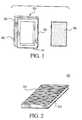
- FIG. 1is an illustration of an exemplary embodiment of a chip carrier and a semiconductor chip
- FIG. 2is an illustration of an exemplary embodiment of a slotted file wall
- FIG. 3is an illustration of an exemplary embodiment of a slotted file
- FIG. 4is an illustration of the stacking process in an exemplary embodiment
- FIG. 5is an illustration of an exemplary embodiment of a completed cube.
- FIG. 1is an illustration of an exemplary embodiment of a chip carrier 100 and a semiconductor chip 108 .
- the chip carrier 100is composed of a floor 102 and a frame 104 .
- the chip carrier 100may be designed to hold the semiconductor chip 108 .
- the floor 102may be a three-dimensional rectangle having a length, a width, and a thickness.
- the frame 104may be a three-dimensional rectangle with a smaller three-dimensional rectangular center removed.
- the frame 104has a length, a width, and a thickness.
- the frame 104is substantially the same length as the floor 102 ; however, the frame 104 is not as wide as the floor 102 .
- the frame 104is positioned in the center of the floor 102 . Because the width of the floor 102 is greater than the width of the frame 104 , the floor 102 protrudes past the edges of the frame 104 forming two flanges 106 , one on either side of the frame 104 .
- both the floor 102 and the frame 104are formed with ceramic materials, but other materials such as metal and plastic may be used.
- the floor 102contains a plurality of electrodes.
- the frame 104has interior dimensions slightly larger than those of the semiconductor chip 108 .
- the interior dimensions of the frame 104may vary to accommodate a variety of different semiconductor chip 108 dimensions.
- the semiconductor chip 108may be placed in the frame 104 face down on the floor 102 contacting the plurality of electrodes at the appropriate circuit interfaces to form a platelet 404 (see FIG. 4).
- FIG. 2is an illustration of a slotted file wall 200 .
- a slotted file wall 200consists of a wall material 202 and may include a plurality of grooves 204 .
- the wall material 202may be a three-dimensional rectangle having a length, a width, and a thickness. Silicon is the preferred wall material 202 in an exemplary embodiment, but other materials, such as gallium arsenide, may be used.
- the wall material 202may be etched with grooves 204 deep enough to receive the flanges 106 of a chip carrier 100 and less than the thickness of the wall material 202 .
- the depth of the groovesmay be less than 10 mils thick.
- the spacing between the grooves 204may be selected based on design requirements, such as the thickness of the platelets 404 , the number of platelets 404 in a completed cube 500 , and an allocated space limitation (see FIG. 5).
- the allocated space limitationmay be the size of an infrared sensor that contains a completed cube 500 .
- Any etching technique that is compatible with the chosen wall material 202may be used. A standard wet etch or plasma etch process that can produce a substantially straight wall trench may be suitable for this purpose.
- FIG. 3is an illustration of an exemplary embodiment of a slotted file 300 .
- a slotted file 300may consist of two side walls 302 and a back wall 304 . Other embodiments may have additional walls. For example, a front wall, a top, or a bottom may also be part of the slotted file 300 .
- the two side walls 302may be etched with grooves 204 .
- the back wall 304may be a section of the wall material 202 that has not been etched with grooves 204 .
- the dimensions of the slotted file 300are based on the size of the platelets 404 , the number of platelets 404 that will be placed in the slotted file 300 , and the spacing between the platelets 404 in the slotted file 300 (see FIG. 4).
- the back wall 304may be connected to an end of each of the two side walls 302 to form a “U” shape.
- the grooves 204 on the two side walls 302face directly across from each other.
- the three walls 302 , 304may be joined together by conventional methods to form a slotted file 300 . For example, an etching process in which tabs and holes are created to join the walls may be employed.
- FIG. 4is an illustration of the stacking process in an exemplary embodiment.
- the semiconductor chip 108is placed into the chip carrier 100 to form a platelet 404 .
- the platelet 404may be less than 5 mils thick.
- Platelets 404are then fitted into the slotted file 300 by inserting the flanges 106 into the opposing grooves 204 . This may be accomplished by placing the platelet 404 in the vicinity of the opposing grooves 204 and using a shake table to slide the platelet into the opposing grooves 204 .
- the spacing between the platelets 404is maintained by the groove interval and no pressure is required to hold the chips in place because of the rigidity of the slotted file 300 .
- FIG. 5illustrates the completed cube 500 after the platelets 404 have been inserted into the slotted file 300 .
- the platelets 404are uniformly stacked without damage. There may be, for example, two hundred platelets 404 in the completed cube 500 .
- the completed cube 500may be made permanent by immersing the assembly in epoxy. To enable the epoxy to flow between substantially all the layers, the completed cube 500 may be placed in a vacuum chamber. Applying a hard vacuum to the chamber may force the epoxy through substantially all the cracks and layers.
Landscapes
- Engineering & Computer Science (AREA)
- Power Engineering (AREA)
- Microelectronics & Electronic Packaging (AREA)
- Physics & Mathematics (AREA)
- Condensed Matter Physics & Semiconductors (AREA)
- General Physics & Mathematics (AREA)
- Computer Hardware Design (AREA)
- Container, Conveyance, Adherence, Positioning, Of Wafer (AREA)
- Structures Or Materials For Encapsulating Or Coating Semiconductor Devices Or Solid State Devices (AREA)
Abstract
Description
- [0001] The United States Government has acquired certain rights in this invention pursuant to Contract No. DASG60-90-C-0136 awarded by the U.S. Army.
- The present invention relates generally to circuit packages, and more particularly, relates to three-dimensional circuit packages that provide stacking for semiconductor platelets.[0002]
- Three-dimensional integrated circuits are employed in applications in which space is a critical design factor. As the demand for more functionality in less space increases, so does the number of designs using three-dimensional packaging. In addition to the benefit of reducing space, these designs may also realize higher speeds because interconnects between circuit components may be shorter.[0003]
- Memory stacking was the first application of three-dimensional packaging, but now applications range from stacking memory modules to stacking entire systems. Different layers in the stack may have different functionalities. For example, one layer may be a memory layer and another may be a logic layer. It is also possible that the different layers in the stack could have different dimensions.[0004]
- These applications may require the precise stacking of very thin platelets into cubes. Platelets may consist of a semiconductor chip placed in a chip carrier. The platelets themselves may be less than 5 mils thick and there may be as many as sixty platelets stacked in one cube. It is critical that the spacing between the platelets is held to a very tight tolerance and that the platelets are not damaged during the stacking procedure.[0005]
- Typically, the platelets are held in the cubical stack by a very thin layer of epoxy resin between each layer. This epoxy layer may be less than one micron thick. Other bonding materials, such as silicone rubber or eutectic solder alloy, may also be employed. The required spacing dimensions may be maintained by using an apparatus with a calibrated compression arm that applies pressure to the stack while the epoxy is setting. A typical amount of pressure may be ten Newtons of force. With this arrangement, only the overall cube dimensions can be maintained, and great care must be taken to prevent cracking the delicate platelets by excessive pressure. The critical layer to layer spacing is thus a derived property and is based upon the uniformity of the thickness and pressure-flow characteristics of the adhesive layer.[0006]
- It would be desirable to provide a stacking method that provides a very tight spacing tolerance between the platelets and that minimizes damage to the platelets during the stacking process. The invention addresses current limitations and makes the critical spacing a directly controlled property resulting in much higher accuracy potential with a relative independence of the adhesive layers.[0007]
- In accordance with this invention, a method for stacking semiconductor platelets in a three-dimensional circuit package is described. Three walls are connected to form a slotted file. The two side walls have grooves. The grooves on the two walls face directly across from each other. Placing a semiconductor chip into a frame of a chip carrier forms a platelet. The frame is located on the surface of a floor of the chip carrier. The floor protrudes past the sides of the frame forming flanges on each side of the frame. The flanges fit into the groves of the slotted file. The platelets are then inserted into the slotted file forming a completed cube.[0008]
- Preferred embodiments are described below in conjunction with the appended drawing figures, wherein like reference numerals refer to like elements in the various figures, and wherein:[0009]
- FIG. 1 is an illustration of an exemplary embodiment of a chip carrier and a semiconductor chip;[0010]
- FIG. 2 is an illustration of an exemplary embodiment of a slotted file wall;[0011]
- FIG. 3 is an illustration of an exemplary embodiment of a slotted file;[0012]
- FIG. 4 is an illustration of the stacking process in an exemplary embodiment; and[0013]
- FIG. 5 is an illustration of an exemplary embodiment of a completed cube.[0014]
- FIG. 1 is an illustration of an exemplary embodiment of a[0015]
chip carrier 100 and asemiconductor chip 108. Thechip carrier 100 is composed of afloor 102 and aframe 104. Thechip carrier 100 may be designed to hold thesemiconductor chip 108. Thefloor 102 may be a three-dimensional rectangle having a length, a width, and a thickness. Theframe 104 may be a three-dimensional rectangle with a smaller three-dimensional rectangular center removed. Theframe 104 has a length, a width, and a thickness. Theframe 104 is substantially the same length as thefloor 102; however, theframe 104 is not as wide as thefloor 102. - The[0016]
frame 104 is positioned in the center of thefloor 102. Because the width of thefloor 102 is greater than the width of theframe 104, thefloor 102 protrudes past the edges of theframe 104 forming twoflanges 106, one on either side of theframe 104. - In an exemplary embodiment both the[0017]
floor 102 and theframe 104 are formed with ceramic materials, but other materials such as metal and plastic may be used. Thefloor 102 contains a plurality of electrodes. Theframe 104 has interior dimensions slightly larger than those of thesemiconductor chip 108. The interior dimensions of theframe 104 may vary to accommodate a variety ofdifferent semiconductor chip 108 dimensions. Thesemiconductor chip 108 may be placed in theframe 104 face down on thefloor 102 contacting the plurality of electrodes at the appropriate circuit interfaces to form a platelet404 (see FIG. 4). - FIG. 2 is an illustration of a slotted[0018]
file wall 200. A slottedfile wall 200 consists of awall material 202 and may include a plurality ofgrooves 204. Thewall material 202 may be a three-dimensional rectangle having a length, a width, and a thickness. Silicon is the preferredwall material 202 in an exemplary embodiment, but other materials, such as gallium arsenide, may be used. - The[0019]
wall material 202 may be etched withgrooves 204 deep enough to receive theflanges 106 of achip carrier 100 and less than the thickness of thewall material 202. For example, the depth of the grooves may be less than 10 mils thick. The spacing between thegrooves 204 may be selected based on design requirements, such as the thickness of theplatelets 404, the number ofplatelets 404 in a completedcube 500, and an allocated space limitation (see FIG. 5). For example, the allocated space limitation may be the size of an infrared sensor that contains a completedcube 500. Any etching technique that is compatible with the chosenwall material 202 may be used. A standard wet etch or plasma etch process that can produce a substantially straight wall trench may be suitable for this purpose. - FIG. 3 is an illustration of an exemplary embodiment of a slotted[0020]
file 300. A slottedfile 300 may consist of twoside walls 302 and aback wall 304. Other embodiments may have additional walls. For example, a front wall, a top, or a bottom may also be part of the slottedfile 300. The twoside walls 302 may be etched withgrooves 204. Theback wall 304 may be a section of thewall material 202 that has not been etched withgrooves 204. The dimensions of the slottedfile 300 are based on the size of theplatelets 404, the number ofplatelets 404 that will be placed in the slottedfile 300, and the spacing between theplatelets 404 in the slotted file300 (see FIG. 4). - The[0021]
back wall 304 may be connected to an end of each of the twoside walls 302 to form a “U” shape. Thegrooves 204 on the twoside walls 302 face directly across from each other. The threewalls file 300. For example, an etching process in which tabs and holes are created to join the walls may be employed. - FIG. 4 is an illustration of the stacking process in an exemplary embodiment. The[0022]
semiconductor chip 108 is placed into thechip carrier 100 to form aplatelet 404. For example, theplatelet 404 may be less than 5 mils thick.Platelets 404 are then fitted into the slottedfile 300 by inserting theflanges 106 into the opposinggrooves 204. This may be accomplished by placing theplatelet 404 in the vicinity of the opposinggrooves 204 and using a shake table to slide the platelet into the opposinggrooves 204. The spacing between theplatelets 404 is maintained by the groove interval and no pressure is required to hold the chips in place because of the rigidity of the slottedfile 300. - FIG. 5 illustrates the completed[0023]
cube 500 after theplatelets 404 have been inserted into the slottedfile 300. By using a slotted cube arrangement, theplatelets 404 are uniformly stacked without damage. There may be, for example, two hundredplatelets 404 in the completedcube 500. The completedcube 500 may be made permanent by immersing the assembly in epoxy. To enable the epoxy to flow between substantially all the layers, the completedcube 500 may be placed in a vacuum chamber. Applying a hard vacuum to the chamber may force the epoxy through substantially all the cracks and layers. - It should be understood that the illustrated embodiments are exemplary only, and should not be taken as limiting the scope of the present invention.[0024]
Claims (29)
1. A system for stacking platelets, comprising in combination:
a slotted file; and
a plurality of platelets which fit into the slotted file.
2. The system ofclaim 1 , wherein the slotted file has at least three walls.
3. The system ofclaim 2 , wherein the at least three walls are composed of silicon.
4. The system ofclaim 2 , wherein the slotted file has at least two side walls and at least one back wall.
5. The system ofclaim 4 , wherein the at least two side walls have been etched with a plurality of grooves.
6. The system ofclaim 5 , wherein a depth of the plurality of grooves is sufficient to hold each of the plurality of platelets.
7. The system ofclaim 5 , wherein a spacing between the plurality of grooves is determined based on a platelet thickness.
8. The system ofclaim 5 , wherein the spacing between the plurality of grooves is determined based on a number of platelets in a completed cube.
9. The system ofclaim 5 , wherein the spacing between the plurality of grooves is determined based on an allocated space limitation.
10. The system ofclaim 4 , wherein the at least one back wall is connected to an end of each of the at least two side walls to form a “U” shape.
11. The system ofclaim 10 , wherein the plurality of grooves on the at least two side walls face directly across from each other.
12. The system ofclaim 1 , wherein each of the plurality of platelets is comprised of a semiconductor chip placed into a chip carrier.
13. The system ofclaim 12 , wherein the chip carrier has a floor and a frame.
14. The system ofclaim 13 , wherein the floor and the frame are composed of a ceramic material.
15. The system ofclaim 13 , wherein the floor protrudes past at least two edges of the frame forming flanges.
16. The system ofclaim 15 , wherein the flanges fit into the plurality of grooves in the at least two side walls of the slotted file.
17. The system ofclaim 13 , wherein the floor has a plurality of electrodes.
18. The system ofclaim 17 , wherein the semiconductor chip is placed face down on the floor contacting the plurality of electrodes.
19. The system ofclaim 1 , wherein epoxy is used to seal a completed cube.
20. A method for stacking platelets, comprising in combination:
etching grooves into a wall material, wherein at least two side walls with a plurality of grooves and at least one back wall without the grooves is formed;
connecting the at least two side walls and the at least one back wall to form a slotted file; and
inserting a plurality of platelets into the slotted file forming a completed cube.
21. The method ofclaim 20 , further comprising immersing the completed cube in epoxy.
22. The method ofclaim 20 , wherein the wall material is silicon.
23. The method ofclaim 20 , wherein a depth of the plurality of grooves is sufficient to hold each of the plurality of platelets.
24. The method ofclaim 20 , wherein a spacing between the plurality of grooves is determined based on a platelet thickness.
25. The method ofclaim 20 , wherein the spacing between the plurality of grooves is determined based on a number of platelets in the completed cube.
26. The method ofclaim 20 , wherein the spacing between the plurality of grooves is determined based on an allocated space limitation.
27. The method ofclaim 20 , wherein each of the plurality of platelets has at least two flanges that fit into the plurality of grooves.
28. The method ofclaim 20 , wherein each of the plurality of platelets is comprised of a semiconductor chip placed into a chip carrier.
29. A system for stacking platelets, comprising in combination:
a slotted file consisting of at least two side walls and at least one back wall, wherein the at least two side walls and the at least one back wall are composed of silicon, wherein the at least two side walls have been etched with a plurality of grooves, wherein the at least one back wall is connected to an end of each of the at least two side walls to form a “U” shape, and wherein the plurality of grooves on the at least two side walls face directly across from each other; and
a plurality of platelets, wherein each of the plurality of platelets is comprised of a semiconductor chip placed into a chip carrier, wherein the chip carrier has a floor and a frame, wherein the floor and the frame are composed of a ceramic material, wherein the floor protrudes past at least two edges of the frame forming flanges, wherein the flanges fit into the plurality of grooves in the at least two side walls of the slotted file, and wherein epoxy is used to seal a completed cube.
Priority Applications (7)
| Application Number | Priority Date | Filing Date | Title |
|---|---|---|---|
| US10/054,374US6958533B2 (en) | 2002-01-22 | 2002-01-22 | High density 3-D integrated circuit package |
| CA002474070ACA2474070A1 (en) | 2002-01-22 | 2003-01-22 | High density 3-d integrated circuit package |
| JP2003568947AJP2005518103A (en) | 2002-01-22 | 2003-01-22 | High-density three-dimensional integrated circuit package |
| AU2003232883AAU2003232883B2 (en) | 2002-01-22 | 2003-01-22 | High density 3-D integrated circuit package |
| PCT/US2003/001910WO2003069969A2 (en) | 2002-01-22 | 2003-01-22 | High density 3-d integrated circuit package |
| EP03728218AEP1468594A2 (en) | 2002-01-22 | 2003-01-22 | High density 3-d integrated circuit package |
| US11/179,377US7176063B2 (en) | 2002-01-22 | 2005-07-12 | High density 3-D integrated circuit package |
Applications Claiming Priority (1)
| Application Number | Priority Date | Filing Date | Title |
|---|---|---|---|
| US10/054,374US6958533B2 (en) | 2002-01-22 | 2002-01-22 | High density 3-D integrated circuit package |
Related Child Applications (1)
| Application Number | Title | Priority Date | Filing Date |
|---|---|---|---|
| US11/179,377DivisionUS7176063B2 (en) | 2002-01-22 | 2005-07-12 | High density 3-D integrated circuit package |
Publications (2)
| Publication Number | Publication Date |
|---|---|
| US20030137059A1true US20030137059A1 (en) | 2003-07-24 |
| US6958533B2 US6958533B2 (en) | 2005-10-25 |
Family
ID=21990598
Family Applications (2)
| Application Number | Title | Priority Date | Filing Date |
|---|---|---|---|
| US10/054,374Expired - Fee RelatedUS6958533B2 (en) | 2002-01-22 | 2002-01-22 | High density 3-D integrated circuit package |
| US11/179,377Expired - Fee RelatedUS7176063B2 (en) | 2002-01-22 | 2005-07-12 | High density 3-D integrated circuit package |
Family Applications After (1)
| Application Number | Title | Priority Date | Filing Date |
|---|---|---|---|
| US11/179,377Expired - Fee RelatedUS7176063B2 (en) | 2002-01-22 | 2005-07-12 | High density 3-D integrated circuit package |
Country Status (6)
| Country | Link |
|---|---|
| US (2) | US6958533B2 (en) |
| EP (1) | EP1468594A2 (en) |
| JP (1) | JP2005518103A (en) |
| AU (1) | AU2003232883B2 (en) |
| CA (1) | CA2474070A1 (en) |
| WO (1) | WO2003069969A2 (en) |
Families Citing this family (4)
| Publication number | Priority date | Publication date | Assignee | Title |
|---|---|---|---|---|
| US8797563B2 (en)* | 2008-03-31 | 2014-08-05 | Ricoh Company, Ltd. | Approach for printing policy-enabled electronic documents using locked printing |
| JP5246691B2 (en)* | 2008-08-29 | 2013-07-24 | セイコーインスツル株式会社 | Electronic component package |
| US8755197B1 (en)* | 2010-12-31 | 2014-06-17 | Veetle, Inc. | High-density, low-power computer cluster for video streaming |
| DE102015108909B4 (en)* | 2015-06-05 | 2021-02-18 | Infineon Technologies Ag | Arrangement of several power semiconductor chips and method for producing the same |
Citations (33)
| Publication number | Priority date | Publication date | Assignee | Title |
|---|---|---|---|---|
| US3614541A (en)* | 1969-04-08 | 1971-10-19 | North American Rockwell | Package for an electronic assembly |
| US3631325A (en)* | 1970-06-15 | 1971-12-28 | Sperry Rand Corp | Card module and end wall treatment facilitating heat transfer and sliding |
| US4214292A (en)* | 1978-11-30 | 1980-07-22 | Sperry Corporation | Printed circuit board guide spring |
| US4502098A (en)* | 1981-02-10 | 1985-02-26 | Brown David F | Circuit assembly |
| US4646128A (en)* | 1980-09-16 | 1987-02-24 | Irvine Sensors Corporation | High-density electronic processing package--structure and fabrication |
| US4704319A (en)* | 1984-11-23 | 1987-11-03 | Irvine Sensors Corporation | Apparatus and method for fabricating modules comprising stacked circuit-carrying layers |
| US4764846A (en)* | 1987-01-05 | 1988-08-16 | Irvine Sensors Corporation | High density electronic package comprising stacked sub-modules |
| US4868712A (en)* | 1987-02-04 | 1989-09-19 | Woodman John K | Three dimensional integrated circuit package |
| US4983533A (en)* | 1987-10-28 | 1991-01-08 | Irvine Sensors Corporation | High-density electronic modules - process and product |
| US4992378A (en)* | 1988-12-16 | 1991-02-12 | The Royal Institution For The Advancement Of Learning (Mcgill University) | C-DNA encoding human prolactin receptor |
| US5140405A (en)* | 1990-08-30 | 1992-08-18 | Micron Technology, Inc. | Semiconductor assembly utilizing elastomeric single axis conductive interconnect |
| US5172303A (en)* | 1990-11-23 | 1992-12-15 | Motorola, Inc. | Electronic component assembly |
| US5222014A (en)* | 1992-03-02 | 1993-06-22 | Motorola, Inc. | Three-dimensional multi-chip pad array carrier |
| US5266833A (en)* | 1992-03-30 | 1993-11-30 | Capps David F | Integrated circuit bus structure |
| US5276590A (en)* | 1991-10-24 | 1994-01-04 | International Business Machines Corporation | Flex circuit electronic cards |
| US5514904A (en)* | 1993-08-26 | 1996-05-07 | Kabushiki Kaisha Toshiba | Semiconductor device with monocrystalline gate insulating film |
| US5581498A (en)* | 1993-08-13 | 1996-12-03 | Irvine Sensors Corporation | Stack of IC chips in lieu of single IC chip |
| US5688721A (en)* | 1994-03-15 | 1997-11-18 | Irvine Sensors Corporation | 3D stack of IC chips having leads reached by vias through passivation covering access plane |
| US5701233A (en)* | 1995-01-23 | 1997-12-23 | Irvine Sensors Corporation | Stackable modules and multimodular assemblies |
| US5754405A (en)* | 1995-11-20 | 1998-05-19 | Mitsubishi Semiconductor America, Inc. | Stacked dual in-line package assembly |
| US5834339A (en)* | 1996-03-07 | 1998-11-10 | Tessera, Inc. | Methods for providing void-free layers for semiconductor assemblies |
| US5838060A (en)* | 1995-12-12 | 1998-11-17 | Comer; Alan E. | Stacked assemblies of semiconductor packages containing programmable interconnect |
| US5943213A (en)* | 1997-11-03 | 1999-08-24 | R-Amtech International, Inc. | Three-dimensional electronic module |
| US5998864A (en)* | 1995-05-26 | 1999-12-07 | Formfactor, Inc. | Stacking semiconductor devices, particularly memory chips |
| US6014316A (en)* | 1997-06-13 | 2000-01-11 | Irvine Sensors Corporation | IC stack utilizing BGA contacts |
| US6028352A (en)* | 1997-06-13 | 2000-02-22 | Irvine Sensors Corporation | IC stack utilizing secondary leadframes |
| US6072234A (en)* | 1996-12-21 | 2000-06-06 | Irvine Sensors Corporation | Stack of equal layer neo-chips containing encapsulated IC chips of different sizes |
| US6117704A (en)* | 1999-03-31 | 2000-09-12 | Irvine Sensors Corporation | Stackable layers containing encapsulated chips |
| US6207474B1 (en)* | 1998-03-09 | 2001-03-27 | Micron Technology, Inc. | Method of forming a stack of packaged memory die and resulting apparatus |
| US6281577B1 (en)* | 1996-06-28 | 2001-08-28 | Pac Tech-Packaging Technologies Gmbh | Chips arranged in plurality of planes and electrically connected to one another |
| US6314541B1 (en)* | 1996-05-31 | 2001-11-06 | Siemens Aktiengesellschaft | Method for computer-aided signaling in an automatic repeat request procedure |
| US6457515B1 (en)* | 1999-08-06 | 2002-10-01 | The Ohio State University | Two-layered micro channel heat sink, devices and systems incorporating same |
| US6507109B2 (en)* | 1998-03-31 | 2003-01-14 | Micron Technology, Inc. | Vertical surface mount package utilizing a back-to-back semiconductor device module |
Family Cites Families (2)
| Publication number | Priority date | Publication date | Assignee | Title |
|---|---|---|---|---|
| US4922378A (en)* | 1986-08-01 | 1990-05-01 | Texas Instruments Incorporated | Baseboard for orthogonal chip mount |
| JP2534204B2 (en)* | 1987-03-31 | 1996-09-11 | 三菱電機株式会社 | Semiconductor device card |
- 2002
- 2002-01-22USUS10/054,374patent/US6958533B2/ennot_activeExpired - Fee Related
- 2003
- 2003-01-22AUAU2003232883Apatent/AU2003232883B2/ennot_activeCeased
- 2003-01-22CACA002474070Apatent/CA2474070A1/ennot_activeAbandoned
- 2003-01-22EPEP03728218Apatent/EP1468594A2/ennot_activeWithdrawn
- 2003-01-22JPJP2003568947Apatent/JP2005518103A/ennot_activeCeased
- 2003-01-22WOPCT/US2003/001910patent/WO2003069969A2/ennot_activeApplication Discontinuation
- 2005
- 2005-07-12USUS11/179,377patent/US7176063B2/ennot_activeExpired - Fee Related
Patent Citations (33)
| Publication number | Priority date | Publication date | Assignee | Title |
|---|---|---|---|---|
| US3614541A (en)* | 1969-04-08 | 1971-10-19 | North American Rockwell | Package for an electronic assembly |
| US3631325A (en)* | 1970-06-15 | 1971-12-28 | Sperry Rand Corp | Card module and end wall treatment facilitating heat transfer and sliding |
| US4214292A (en)* | 1978-11-30 | 1980-07-22 | Sperry Corporation | Printed circuit board guide spring |
| US4646128A (en)* | 1980-09-16 | 1987-02-24 | Irvine Sensors Corporation | High-density electronic processing package--structure and fabrication |
| US4502098A (en)* | 1981-02-10 | 1985-02-26 | Brown David F | Circuit assembly |
| US4704319A (en)* | 1984-11-23 | 1987-11-03 | Irvine Sensors Corporation | Apparatus and method for fabricating modules comprising stacked circuit-carrying layers |
| US4764846A (en)* | 1987-01-05 | 1988-08-16 | Irvine Sensors Corporation | High density electronic package comprising stacked sub-modules |
| US4868712A (en)* | 1987-02-04 | 1989-09-19 | Woodman John K | Three dimensional integrated circuit package |
| US4983533A (en)* | 1987-10-28 | 1991-01-08 | Irvine Sensors Corporation | High-density electronic modules - process and product |
| US4992378A (en)* | 1988-12-16 | 1991-02-12 | The Royal Institution For The Advancement Of Learning (Mcgill University) | C-DNA encoding human prolactin receptor |
| US5140405A (en)* | 1990-08-30 | 1992-08-18 | Micron Technology, Inc. | Semiconductor assembly utilizing elastomeric single axis conductive interconnect |
| US5172303A (en)* | 1990-11-23 | 1992-12-15 | Motorola, Inc. | Electronic component assembly |
| US5276590A (en)* | 1991-10-24 | 1994-01-04 | International Business Machines Corporation | Flex circuit electronic cards |
| US5222014A (en)* | 1992-03-02 | 1993-06-22 | Motorola, Inc. | Three-dimensional multi-chip pad array carrier |
| US5266833A (en)* | 1992-03-30 | 1993-11-30 | Capps David F | Integrated circuit bus structure |
| US5581498A (en)* | 1993-08-13 | 1996-12-03 | Irvine Sensors Corporation | Stack of IC chips in lieu of single IC chip |
| US5514904A (en)* | 1993-08-26 | 1996-05-07 | Kabushiki Kaisha Toshiba | Semiconductor device with monocrystalline gate insulating film |
| US5688721A (en)* | 1994-03-15 | 1997-11-18 | Irvine Sensors Corporation | 3D stack of IC chips having leads reached by vias through passivation covering access plane |
| US5701233A (en)* | 1995-01-23 | 1997-12-23 | Irvine Sensors Corporation | Stackable modules and multimodular assemblies |
| US5998864A (en)* | 1995-05-26 | 1999-12-07 | Formfactor, Inc. | Stacking semiconductor devices, particularly memory chips |
| US5754405A (en)* | 1995-11-20 | 1998-05-19 | Mitsubishi Semiconductor America, Inc. | Stacked dual in-line package assembly |
| US5838060A (en)* | 1995-12-12 | 1998-11-17 | Comer; Alan E. | Stacked assemblies of semiconductor packages containing programmable interconnect |
| US5834339A (en)* | 1996-03-07 | 1998-11-10 | Tessera, Inc. | Methods for providing void-free layers for semiconductor assemblies |
| US6314541B1 (en)* | 1996-05-31 | 2001-11-06 | Siemens Aktiengesellschaft | Method for computer-aided signaling in an automatic repeat request procedure |
| US6281577B1 (en)* | 1996-06-28 | 2001-08-28 | Pac Tech-Packaging Technologies Gmbh | Chips arranged in plurality of planes and electrically connected to one another |
| US6072234A (en)* | 1996-12-21 | 2000-06-06 | Irvine Sensors Corporation | Stack of equal layer neo-chips containing encapsulated IC chips of different sizes |
| US6014316A (en)* | 1997-06-13 | 2000-01-11 | Irvine Sensors Corporation | IC stack utilizing BGA contacts |
| US6028352A (en)* | 1997-06-13 | 2000-02-22 | Irvine Sensors Corporation | IC stack utilizing secondary leadframes |
| US5943213A (en)* | 1997-11-03 | 1999-08-24 | R-Amtech International, Inc. | Three-dimensional electronic module |
| US6207474B1 (en)* | 1998-03-09 | 2001-03-27 | Micron Technology, Inc. | Method of forming a stack of packaged memory die and resulting apparatus |
| US6507109B2 (en)* | 1998-03-31 | 2003-01-14 | Micron Technology, Inc. | Vertical surface mount package utilizing a back-to-back semiconductor device module |
| US6117704A (en)* | 1999-03-31 | 2000-09-12 | Irvine Sensors Corporation | Stackable layers containing encapsulated chips |
| US6457515B1 (en)* | 1999-08-06 | 2002-10-01 | The Ohio State University | Two-layered micro channel heat sink, devices and systems incorporating same |
Also Published As
| Publication number | Publication date |
|---|---|
| US7176063B2 (en) | 2007-02-13 |
| US6958533B2 (en) | 2005-10-25 |
| WO2003069969A2 (en) | 2003-08-21 |
| WO2003069969A3 (en) | 2004-05-13 |
| EP1468594A2 (en) | 2004-10-20 |
| AU2003232883B2 (en) | 2006-07-13 |
| AU2003232883A1 (en) | 2003-09-04 |
| JP2005518103A (en) | 2005-06-16 |
| US20050263870A1 (en) | 2005-12-01 |
| CA2474070A1 (en) | 2003-08-21 |
Similar Documents
| Publication | Publication Date | Title |
|---|---|---|
| CN211350641U (en) | Electronic device | |
| US8647923B2 (en) | Method of manufacturing semiconductor device | |
| US5885850A (en) | Method for the 3D interconnection of packages of electronic components, and device obtained by this method | |
| Zoschke et al. | Hermetic wafer level packaging of MEMS components using through silicon via and wafer to wafer bonding technologies | |
| US20080124835A1 (en) | Hermetic seal and reliable bonding structures for 3d applications | |
| EP0706219A1 (en) | Method and apparatus for a stress relieved electronic module | |
| CN111627893B (en) | TSV semiconductor device including two-dimensional shift | |
| US6809424B2 (en) | Method for making electronic devices including silicon and LTCC and devices produced thereby | |
| US6958533B2 (en) | High density 3-D integrated circuit package | |
| US6972243B2 (en) | Fabrication of semiconductor dies with micro-pins and structures produced therewith | |
| EP2652782A2 (en) | Void-free wafer bonding using channels | |
| US10453706B2 (en) | Methods and devices for miniaturization of high density wafer based electronic 3D multi-chip modules | |
| CN113921473A (en) | Packaging structure and manufacturing method thereof | |
| CN112928077A (en) | Multi-chip heterogeneous integrated packaging unit and manufacturing method and stacking structure thereof | |
| US10269667B2 (en) | Semiconductor device packaging with reduced size and delamination | |
| US20250157999A1 (en) | Chip package structure, electronic device, and packaging method of chip package structure | |
| US20240186208A1 (en) | Method, structure, and manufacturing method for expanding chip heat dissipation area | |
| US20250201616A1 (en) | Semiconductor manufacturing device and semiconductor device manufacturing method | |
| US20240203822A1 (en) | Thermal expansion matched chip module with integrated liquid cooling | |
| KR20010058357A (en) | Dual chip Package of socket type | |
| JPS58218136A (en) | Die collet for semiconductor device | |
| CN108946652B (en) | Semiconductor device packaging and method of manufacturing same | |
| TW202405897A (en) | Semiconductor device and methods of manufacturing thereof | |
| KR20050041095A (en) | Multi-chip exposed lead package and stack thereof | |
| TWM240057U (en) | Multiple-step inner lead of leadframe |
Legal Events
| Date | Code | Title | Description |
|---|---|---|---|
| AS | Assignment | Owner name:HONEYWELL INTERNATIONAL INC., NEW JERSEY Free format text:ASSIGNMENT OF ASSIGNORS INTEREST;ASSIGNORS:SULLIVAN, GERARD J.;ADKINS, LARRY R.;HUGHES, A. JAMES;REEL/FRAME:012524/0121;SIGNING DATES FROM 20011016 TO 20011113 | |
| CC | Certificate of correction | ||
| FPAY | Fee payment | Year of fee payment:4 | |
| REMI | Maintenance fee reminder mailed | ||
| LAPS | Lapse for failure to pay maintenance fees | ||
| STCH | Information on status: patent discontinuation | Free format text:PATENT EXPIRED DUE TO NONPAYMENT OF MAINTENANCE FEES UNDER 37 CFR 1.362 | |
| FP | Lapsed due to failure to pay maintenance fee | Effective date:20131025 |