US20030136814A1 - High density raised stud microjoining system and methods of fabricating the same - Google Patents
High density raised stud microjoining system and methods of fabricating the sameDownload PDFInfo
- Publication number
- US20030136814A1 US20030136814A1US10/052,591US5259102AUS2003136814A1US 20030136814 A1US20030136814 A1US 20030136814A1US 5259102 AUS5259102 AUS 5259102AUS 2003136814 A1US2003136814 A1US 2003136814A1
- Authority
- US
- United States
- Prior art keywords
- carrier
- receptacles
- layer
- dielectric layer
- device chips
- Prior art date
- Legal status (The legal status is an assumption and is not a legal conclusion. Google has not performed a legal analysis and makes no representation as to the accuracy of the status listed.)
- Granted
Links
Images


Classifications
- H—ELECTRICITY
- H01—ELECTRIC ELEMENTS
- H01L—SEMICONDUCTOR DEVICES NOT COVERED BY CLASS H10
- H01L24/00—Arrangements for connecting or disconnecting semiconductor or solid-state bodies; Methods or apparatus related thereto
- H01L24/01—Means for bonding being attached to, or being formed on, the surface to be connected, e.g. chip-to-package, die-attach, "first-level" interconnects; Manufacturing methods related thereto
- H01L24/10—Bump connectors ; Manufacturing methods related thereto
- H01L24/12—Structure, shape, material or disposition of the bump connectors prior to the connecting process
- H—ELECTRICITY
- H01—ELECTRIC ELEMENTS
- H01L—SEMICONDUCTOR DEVICES NOT COVERED BY CLASS H10
- H01L21/00—Processes or apparatus adapted for the manufacture or treatment of semiconductor or solid state devices or of parts thereof
- H01L21/02—Manufacture or treatment of semiconductor devices or of parts thereof
- H01L21/04—Manufacture or treatment of semiconductor devices or of parts thereof the devices having potential barriers, e.g. a PN junction, depletion layer or carrier concentration layer
- H01L21/18—Manufacture or treatment of semiconductor devices or of parts thereof the devices having potential barriers, e.g. a PN junction, depletion layer or carrier concentration layer the devices having semiconductor bodies comprising elements of Group IV of the Periodic Table or AIIIBV compounds with or without impurities, e.g. doping materials
- H01L21/28—Manufacture of electrodes on semiconductor bodies using processes or apparatus not provided for in groups H01L21/20 - H01L21/268
- H01L21/283—Deposition of conductive or insulating materials for electrodes conducting electric current
- H01L21/288—Deposition of conductive or insulating materials for electrodes conducting electric current from a liquid, e.g. electrolytic deposition
- H01L21/2885—Deposition of conductive or insulating materials for electrodes conducting electric current from a liquid, e.g. electrolytic deposition using an external electrical current, i.e. electro-deposition
- H—ELECTRICITY
- H01—ELECTRIC ELEMENTS
- H01L—SEMICONDUCTOR DEVICES NOT COVERED BY CLASS H10
- H01L24/00—Arrangements for connecting or disconnecting semiconductor or solid-state bodies; Methods or apparatus related thereto
- H01L24/01—Means for bonding being attached to, or being formed on, the surface to be connected, e.g. chip-to-package, die-attach, "first-level" interconnects; Manufacturing methods related thereto
- H01L24/02—Bonding areas ; Manufacturing methods related thereto
- H01L24/03—Manufacturing methods
- H—ELECTRICITY
- H01—ELECTRIC ELEMENTS
- H01L—SEMICONDUCTOR DEVICES NOT COVERED BY CLASS H10
- H01L24/00—Arrangements for connecting or disconnecting semiconductor or solid-state bodies; Methods or apparatus related thereto
- H01L24/01—Means for bonding being attached to, or being formed on, the surface to be connected, e.g. chip-to-package, die-attach, "first-level" interconnects; Manufacturing methods related thereto
- H01L24/02—Bonding areas ; Manufacturing methods related thereto
- H01L24/04—Structure, shape, material or disposition of the bonding areas prior to the connecting process
- H01L24/05—Structure, shape, material or disposition of the bonding areas prior to the connecting process of an individual bonding area
- H—ELECTRICITY
- H01—ELECTRIC ELEMENTS
- H01L—SEMICONDUCTOR DEVICES NOT COVERED BY CLASS H10
- H01L24/00—Arrangements for connecting or disconnecting semiconductor or solid-state bodies; Methods or apparatus related thereto
- H01L24/01—Means for bonding being attached to, or being formed on, the surface to be connected, e.g. chip-to-package, die-attach, "first-level" interconnects; Manufacturing methods related thereto
- H01L24/10—Bump connectors ; Manufacturing methods related thereto
- H01L24/11—Manufacturing methods
- H—ELECTRICITY
- H01—ELECTRIC ELEMENTS
- H01L—SEMICONDUCTOR DEVICES NOT COVERED BY CLASS H10
- H01L24/00—Arrangements for connecting or disconnecting semiconductor or solid-state bodies; Methods or apparatus related thereto
- H01L24/01—Means for bonding being attached to, or being formed on, the surface to be connected, e.g. chip-to-package, die-attach, "first-level" interconnects; Manufacturing methods related thereto
- H01L24/10—Bump connectors ; Manufacturing methods related thereto
- H01L24/15—Structure, shape, material or disposition of the bump connectors after the connecting process
- H01L24/16—Structure, shape, material or disposition of the bump connectors after the connecting process of an individual bump connector
- H—ELECTRICITY
- H05—ELECTRIC TECHNIQUES NOT OTHERWISE PROVIDED FOR
- H05K—PRINTED CIRCUITS; CASINGS OR CONSTRUCTIONAL DETAILS OF ELECTRIC APPARATUS; MANUFACTURE OF ASSEMBLAGES OF ELECTRICAL COMPONENTS
- H05K1/00—Printed circuits
- H05K1/02—Details
- H05K1/11—Printed elements for providing electric connections to or between printed circuits
- H05K1/111—Pads for surface mounting, e.g. lay-out
- H05K1/112—Pads for surface mounting, e.g. lay-out directly combined with via connections
- H—ELECTRICITY
- H01—ELECTRIC ELEMENTS
- H01L—SEMICONDUCTOR DEVICES NOT COVERED BY CLASS H10
- H01L2224/00—Indexing scheme for arrangements for connecting or disconnecting semiconductor or solid-state bodies and methods related thereto as covered by H01L24/00
- H01L2224/01—Means for bonding being attached to, or being formed on, the surface to be connected, e.g. chip-to-package, die-attach, "first-level" interconnects; Manufacturing methods related thereto
- H01L2224/02—Bonding areas; Manufacturing methods related thereto
- H01L2224/04—Structure, shape, material or disposition of the bonding areas prior to the connecting process
- H01L2224/0401—Bonding areas specifically adapted for bump connectors, e.g. under bump metallisation [UBM]
- H—ELECTRICITY
- H01—ELECTRIC ELEMENTS
- H01L—SEMICONDUCTOR DEVICES NOT COVERED BY CLASS H10
- H01L2224/00—Indexing scheme for arrangements for connecting or disconnecting semiconductor or solid-state bodies and methods related thereto as covered by H01L24/00
- H01L2224/01—Means for bonding being attached to, or being formed on, the surface to be connected, e.g. chip-to-package, die-attach, "first-level" interconnects; Manufacturing methods related thereto
- H01L2224/02—Bonding areas; Manufacturing methods related thereto
- H01L2224/04—Structure, shape, material or disposition of the bonding areas prior to the connecting process
- H01L2224/05—Structure, shape, material or disposition of the bonding areas prior to the connecting process of an individual bonding area
- H01L2224/0554—External layer
- H01L2224/0556—Disposition
- H01L2224/05571—Disposition the external layer being disposed in a recess of the surface
- H—ELECTRICITY
- H01—ELECTRIC ELEMENTS
- H01L—SEMICONDUCTOR DEVICES NOT COVERED BY CLASS H10
- H01L2224/00—Indexing scheme for arrangements for connecting or disconnecting semiconductor or solid-state bodies and methods related thereto as covered by H01L24/00
- H01L2224/01—Means for bonding being attached to, or being formed on, the surface to be connected, e.g. chip-to-package, die-attach, "first-level" interconnects; Manufacturing methods related thereto
- H01L2224/02—Bonding areas; Manufacturing methods related thereto
- H01L2224/04—Structure, shape, material or disposition of the bonding areas prior to the connecting process
- H01L2224/05—Structure, shape, material or disposition of the bonding areas prior to the connecting process of an individual bonding area
- H01L2224/0554—External layer
- H01L2224/05599—Material
- H—ELECTRICITY
- H01—ELECTRIC ELEMENTS
- H01L—SEMICONDUCTOR DEVICES NOT COVERED BY CLASS H10
- H01L2224/00—Indexing scheme for arrangements for connecting or disconnecting semiconductor or solid-state bodies and methods related thereto as covered by H01L24/00
- H01L2224/01—Means for bonding being attached to, or being formed on, the surface to be connected, e.g. chip-to-package, die-attach, "first-level" interconnects; Manufacturing methods related thereto
- H01L2224/10—Bump connectors; Manufacturing methods related thereto
- H01L2224/11—Manufacturing methods
- H01L2224/114—Manufacturing methods by blanket deposition of the material of the bump connector
- H01L2224/1146—Plating
- H—ELECTRICITY
- H01—ELECTRIC ELEMENTS
- H01L—SEMICONDUCTOR DEVICES NOT COVERED BY CLASS H10
- H01L2224/00—Indexing scheme for arrangements for connecting or disconnecting semiconductor or solid-state bodies and methods related thereto as covered by H01L24/00
- H01L2224/01—Means for bonding being attached to, or being formed on, the surface to be connected, e.g. chip-to-package, die-attach, "first-level" interconnects; Manufacturing methods related thereto
- H01L2224/10—Bump connectors; Manufacturing methods related thereto
- H01L2224/11—Manufacturing methods
- H01L2224/1147—Manufacturing methods using a lift-off mask
- H—ELECTRICITY
- H01—ELECTRIC ELEMENTS
- H01L—SEMICONDUCTOR DEVICES NOT COVERED BY CLASS H10
- H01L2224/00—Indexing scheme for arrangements for connecting or disconnecting semiconductor or solid-state bodies and methods related thereto as covered by H01L24/00
- H01L2224/01—Means for bonding being attached to, or being formed on, the surface to be connected, e.g. chip-to-package, die-attach, "first-level" interconnects; Manufacturing methods related thereto
- H01L2224/10—Bump connectors; Manufacturing methods related thereto
- H01L2224/11—Manufacturing methods
- H01L2224/118—Post-treatment of the bump connector
- H01L2224/11848—Thermal treatments, e.g. annealing, controlled cooling
- H01L2224/11849—Reflowing
- H—ELECTRICITY
- H01—ELECTRIC ELEMENTS
- H01L—SEMICONDUCTOR DEVICES NOT COVERED BY CLASS H10
- H01L2224/00—Indexing scheme for arrangements for connecting or disconnecting semiconductor or solid-state bodies and methods related thereto as covered by H01L24/00
- H01L2224/01—Means for bonding being attached to, or being formed on, the surface to be connected, e.g. chip-to-package, die-attach, "first-level" interconnects; Manufacturing methods related thereto
- H01L2224/10—Bump connectors; Manufacturing methods related thereto
- H01L2224/12—Structure, shape, material or disposition of the bump connectors prior to the connecting process
- H01L2224/13—Structure, shape, material or disposition of the bump connectors prior to the connecting process of an individual bump connector
- H01L2224/13001—Core members of the bump connector
- H01L2224/1302—Disposition
- H01L2224/13022—Disposition the bump connector being at least partially embedded in the surface
- H—ELECTRICITY
- H01—ELECTRIC ELEMENTS
- H01L—SEMICONDUCTOR DEVICES NOT COVERED BY CLASS H10
- H01L2224/00—Indexing scheme for arrangements for connecting or disconnecting semiconductor or solid-state bodies and methods related thereto as covered by H01L24/00
- H01L2224/01—Means for bonding being attached to, or being formed on, the surface to be connected, e.g. chip-to-package, die-attach, "first-level" interconnects; Manufacturing methods related thereto
- H01L2224/10—Bump connectors; Manufacturing methods related thereto
- H01L2224/12—Structure, shape, material or disposition of the bump connectors prior to the connecting process
- H01L2224/13—Structure, shape, material or disposition of the bump connectors prior to the connecting process of an individual bump connector
- H01L2224/13001—Core members of the bump connector
- H01L2224/13075—Plural core members
- H01L2224/1308—Plural core members being stacked
- H01L2224/13083—Three-layer arrangements
- H—ELECTRICITY
- H01—ELECTRIC ELEMENTS
- H01L—SEMICONDUCTOR DEVICES NOT COVERED BY CLASS H10
- H01L2224/00—Indexing scheme for arrangements for connecting or disconnecting semiconductor or solid-state bodies and methods related thereto as covered by H01L24/00
- H01L2224/01—Means for bonding being attached to, or being formed on, the surface to be connected, e.g. chip-to-package, die-attach, "first-level" interconnects; Manufacturing methods related thereto
- H01L2224/10—Bump connectors; Manufacturing methods related thereto
- H01L2224/12—Structure, shape, material or disposition of the bump connectors prior to the connecting process
- H01L2224/13—Structure, shape, material or disposition of the bump connectors prior to the connecting process of an individual bump connector
- H01L2224/13001—Core members of the bump connector
- H01L2224/13099—Material
- H01L2224/131—Material with a principal constituent of the material being a metal or a metalloid, e.g. boron [B], silicon [Si], germanium [Ge], arsenic [As], antimony [Sb], tellurium [Te] and polonium [Po], and alloys thereof
- H01L2224/13101—Material with a principal constituent of the material being a metal or a metalloid, e.g. boron [B], silicon [Si], germanium [Ge], arsenic [As], antimony [Sb], tellurium [Te] and polonium [Po], and alloys thereof the principal constituent melting at a temperature of less than 400°C
- H01L2224/13116—Lead [Pb] as principal constituent
- H—ELECTRICITY
- H01—ELECTRIC ELEMENTS
- H01L—SEMICONDUCTOR DEVICES NOT COVERED BY CLASS H10
- H01L2224/00—Indexing scheme for arrangements for connecting or disconnecting semiconductor or solid-state bodies and methods related thereto as covered by H01L24/00
- H01L2224/01—Means for bonding being attached to, or being formed on, the surface to be connected, e.g. chip-to-package, die-attach, "first-level" interconnects; Manufacturing methods related thereto
- H01L2224/10—Bump connectors; Manufacturing methods related thereto
- H01L2224/12—Structure, shape, material or disposition of the bump connectors prior to the connecting process
- H01L2224/13—Structure, shape, material or disposition of the bump connectors prior to the connecting process of an individual bump connector
- H01L2224/13001—Core members of the bump connector
- H01L2224/13099—Material
- H01L2224/131—Material with a principal constituent of the material being a metal or a metalloid, e.g. boron [B], silicon [Si], germanium [Ge], arsenic [As], antimony [Sb], tellurium [Te] and polonium [Po], and alloys thereof
- H01L2224/13138—Material with a principal constituent of the material being a metal or a metalloid, e.g. boron [B], silicon [Si], germanium [Ge], arsenic [As], antimony [Sb], tellurium [Te] and polonium [Po], and alloys thereof the principal constituent melting at a temperature of greater than or equal to 950°C and less than 1550°C
- H01L2224/13144—Gold [Au] as principal constituent
- H—ELECTRICITY
- H01—ELECTRIC ELEMENTS
- H01L—SEMICONDUCTOR DEVICES NOT COVERED BY CLASS H10
- H01L2224/00—Indexing scheme for arrangements for connecting or disconnecting semiconductor or solid-state bodies and methods related thereto as covered by H01L24/00
- H01L2224/01—Means for bonding being attached to, or being formed on, the surface to be connected, e.g. chip-to-package, die-attach, "first-level" interconnects; Manufacturing methods related thereto
- H01L2224/10—Bump connectors; Manufacturing methods related thereto
- H01L2224/12—Structure, shape, material or disposition of the bump connectors prior to the connecting process
- H01L2224/13—Structure, shape, material or disposition of the bump connectors prior to the connecting process of an individual bump connector
- H01L2224/13001—Core members of the bump connector
- H01L2224/13099—Material
- H01L2224/131—Material with a principal constituent of the material being a metal or a metalloid, e.g. boron [B], silicon [Si], germanium [Ge], arsenic [As], antimony [Sb], tellurium [Te] and polonium [Po], and alloys thereof
- H01L2224/13138—Material with a principal constituent of the material being a metal or a metalloid, e.g. boron [B], silicon [Si], germanium [Ge], arsenic [As], antimony [Sb], tellurium [Te] and polonium [Po], and alloys thereof the principal constituent melting at a temperature of greater than or equal to 950°C and less than 1550°C
- H01L2224/13147—Copper [Cu] as principal constituent
- H—ELECTRICITY
- H01—ELECTRIC ELEMENTS
- H01L—SEMICONDUCTOR DEVICES NOT COVERED BY CLASS H10
- H01L2224/00—Indexing scheme for arrangements for connecting or disconnecting semiconductor or solid-state bodies and methods related thereto as covered by H01L24/00
- H01L2224/01—Means for bonding being attached to, or being formed on, the surface to be connected, e.g. chip-to-package, die-attach, "first-level" interconnects; Manufacturing methods related thereto
- H01L2224/10—Bump connectors; Manufacturing methods related thereto
- H01L2224/12—Structure, shape, material or disposition of the bump connectors prior to the connecting process
- H01L2224/13—Structure, shape, material or disposition of the bump connectors prior to the connecting process of an individual bump connector
- H01L2224/13001—Core members of the bump connector
- H01L2224/13099—Material
- H01L2224/131—Material with a principal constituent of the material being a metal or a metalloid, e.g. boron [B], silicon [Si], germanium [Ge], arsenic [As], antimony [Sb], tellurium [Te] and polonium [Po], and alloys thereof
- H01L2224/13138—Material with a principal constituent of the material being a metal or a metalloid, e.g. boron [B], silicon [Si], germanium [Ge], arsenic [As], antimony [Sb], tellurium [Te] and polonium [Po], and alloys thereof the principal constituent melting at a temperature of greater than or equal to 950°C and less than 1550°C
- H01L2224/13155—Nickel [Ni] as principal constituent
- H—ELECTRICITY
- H01—ELECTRIC ELEMENTS
- H01L—SEMICONDUCTOR DEVICES NOT COVERED BY CLASS H10
- H01L2224/00—Indexing scheme for arrangements for connecting or disconnecting semiconductor or solid-state bodies and methods related thereto as covered by H01L24/00
- H01L2224/01—Means for bonding being attached to, or being formed on, the surface to be connected, e.g. chip-to-package, die-attach, "first-level" interconnects; Manufacturing methods related thereto
- H01L2224/10—Bump connectors; Manufacturing methods related thereto
- H01L2224/12—Structure, shape, material or disposition of the bump connectors prior to the connecting process
- H01L2224/13—Structure, shape, material or disposition of the bump connectors prior to the connecting process of an individual bump connector
- H01L2224/13001—Core members of the bump connector
- H01L2224/13099—Material
- H01L2224/131—Material with a principal constituent of the material being a metal or a metalloid, e.g. boron [B], silicon [Si], germanium [Ge], arsenic [As], antimony [Sb], tellurium [Te] and polonium [Po], and alloys thereof
- H01L2224/13138—Material with a principal constituent of the material being a metal or a metalloid, e.g. boron [B], silicon [Si], germanium [Ge], arsenic [As], antimony [Sb], tellurium [Te] and polonium [Po], and alloys thereof the principal constituent melting at a temperature of greater than or equal to 950°C and less than 1550°C
- H01L2224/13157—Cobalt [Co] as principal constituent
- H—ELECTRICITY
- H01—ELECTRIC ELEMENTS
- H01L—SEMICONDUCTOR DEVICES NOT COVERED BY CLASS H10
- H01L2224/00—Indexing scheme for arrangements for connecting or disconnecting semiconductor or solid-state bodies and methods related thereto as covered by H01L24/00
- H01L2224/01—Means for bonding being attached to, or being formed on, the surface to be connected, e.g. chip-to-package, die-attach, "first-level" interconnects; Manufacturing methods related thereto
- H01L2224/10—Bump connectors; Manufacturing methods related thereto
- H01L2224/12—Structure, shape, material or disposition of the bump connectors prior to the connecting process
- H01L2224/13—Structure, shape, material or disposition of the bump connectors prior to the connecting process of an individual bump connector
- H01L2224/13001—Core members of the bump connector
- H01L2224/13099—Material
- H01L2224/131—Material with a principal constituent of the material being a metal or a metalloid, e.g. boron [B], silicon [Si], germanium [Ge], arsenic [As], antimony [Sb], tellurium [Te] and polonium [Po], and alloys thereof
- H01L2224/13163—Material with a principal constituent of the material being a metal or a metalloid, e.g. boron [B], silicon [Si], germanium [Ge], arsenic [As], antimony [Sb], tellurium [Te] and polonium [Po], and alloys thereof the principal constituent melting at a temperature of greater than 1550°C
- H01L2224/13164—Palladium [Pd] as principal constituent
- H—ELECTRICITY
- H01—ELECTRIC ELEMENTS
- H01L—SEMICONDUCTOR DEVICES NOT COVERED BY CLASS H10
- H01L2224/00—Indexing scheme for arrangements for connecting or disconnecting semiconductor or solid-state bodies and methods related thereto as covered by H01L24/00
- H01L2224/01—Means for bonding being attached to, or being formed on, the surface to be connected, e.g. chip-to-package, die-attach, "first-level" interconnects; Manufacturing methods related thereto
- H01L2224/10—Bump connectors; Manufacturing methods related thereto
- H01L2224/12—Structure, shape, material or disposition of the bump connectors prior to the connecting process
- H01L2224/13—Structure, shape, material or disposition of the bump connectors prior to the connecting process of an individual bump connector
- H01L2224/13001—Core members of the bump connector
- H01L2224/13099—Material
- H01L2224/131—Material with a principal constituent of the material being a metal or a metalloid, e.g. boron [B], silicon [Si], germanium [Ge], arsenic [As], antimony [Sb], tellurium [Te] and polonium [Po], and alloys thereof
- H01L2224/13163—Material with a principal constituent of the material being a metal or a metalloid, e.g. boron [B], silicon [Si], germanium [Ge], arsenic [As], antimony [Sb], tellurium [Te] and polonium [Po], and alloys thereof the principal constituent melting at a temperature of greater than 1550°C
- H01L2224/13169—Platinum [Pt] as principal constituent
- H—ELECTRICITY
- H01—ELECTRIC ELEMENTS
- H01L—SEMICONDUCTOR DEVICES NOT COVERED BY CLASS H10
- H01L2224/00—Indexing scheme for arrangements for connecting or disconnecting semiconductor or solid-state bodies and methods related thereto as covered by H01L24/00
- H01L2224/01—Means for bonding being attached to, or being formed on, the surface to be connected, e.g. chip-to-package, die-attach, "first-level" interconnects; Manufacturing methods related thereto
- H01L2224/10—Bump connectors; Manufacturing methods related thereto
- H01L2224/12—Structure, shape, material or disposition of the bump connectors prior to the connecting process
- H01L2224/13—Structure, shape, material or disposition of the bump connectors prior to the connecting process of an individual bump connector
- H01L2224/1354—Coating
- H01L2224/13575—Plural coating layers
- H01L2224/1358—Plural coating layers being stacked
- H01L2224/13582—Two-layer coating
- H—ELECTRICITY
- H01—ELECTRIC ELEMENTS
- H01L—SEMICONDUCTOR DEVICES NOT COVERED BY CLASS H10
- H01L2224/00—Indexing scheme for arrangements for connecting or disconnecting semiconductor or solid-state bodies and methods related thereto as covered by H01L24/00
- H01L2224/01—Means for bonding being attached to, or being formed on, the surface to be connected, e.g. chip-to-package, die-attach, "first-level" interconnects; Manufacturing methods related thereto
- H01L2224/10—Bump connectors; Manufacturing methods related thereto
- H01L2224/12—Structure, shape, material or disposition of the bump connectors prior to the connecting process
- H01L2224/13—Structure, shape, material or disposition of the bump connectors prior to the connecting process of an individual bump connector
- H01L2224/1354—Coating
- H01L2224/13599—Material
- H01L2224/136—Material with a principal constituent of the material being a metal or a metalloid, e.g. boron [B], silicon [Si], germanium [Ge], arsenic [As], antimony [Sb], tellurium [Te] and polonium [Po], and alloys thereof
- H01L2224/13601—Material with a principal constituent of the material being a metal or a metalloid, e.g. boron [B], silicon [Si], germanium [Ge], arsenic [As], antimony [Sb], tellurium [Te] and polonium [Po], and alloys thereof the principal constituent melting at a temperature of less than 400°C
- H01L2224/13616—Lead [Pb] as principal constituent
- H—ELECTRICITY
- H01—ELECTRIC ELEMENTS
- H01L—SEMICONDUCTOR DEVICES NOT COVERED BY CLASS H10
- H01L2224/00—Indexing scheme for arrangements for connecting or disconnecting semiconductor or solid-state bodies and methods related thereto as covered by H01L24/00
- H01L2224/01—Means for bonding being attached to, or being formed on, the surface to be connected, e.g. chip-to-package, die-attach, "first-level" interconnects; Manufacturing methods related thereto
- H01L2224/10—Bump connectors; Manufacturing methods related thereto
- H01L2224/12—Structure, shape, material or disposition of the bump connectors prior to the connecting process
- H01L2224/13—Structure, shape, material or disposition of the bump connectors prior to the connecting process of an individual bump connector
- H01L2224/1354—Coating
- H01L2224/13599—Material
- H01L2224/136—Material with a principal constituent of the material being a metal or a metalloid, e.g. boron [B], silicon [Si], germanium [Ge], arsenic [As], antimony [Sb], tellurium [Te] and polonium [Po], and alloys thereof
- H01L2224/13638—Material with a principal constituent of the material being a metal or a metalloid, e.g. boron [B], silicon [Si], germanium [Ge], arsenic [As], antimony [Sb], tellurium [Te] and polonium [Po], and alloys thereof the principal constituent melting at a temperature of greater than or equal to 950°C and less than 1550°C
- H01L2224/13644—Gold [Au] as principal constituent
- H—ELECTRICITY
- H01—ELECTRIC ELEMENTS
- H01L—SEMICONDUCTOR DEVICES NOT COVERED BY CLASS H10
- H01L2224/00—Indexing scheme for arrangements for connecting or disconnecting semiconductor or solid-state bodies and methods related thereto as covered by H01L24/00
- H01L2224/01—Means for bonding being attached to, or being formed on, the surface to be connected, e.g. chip-to-package, die-attach, "first-level" interconnects; Manufacturing methods related thereto
- H01L2224/10—Bump connectors; Manufacturing methods related thereto
- H01L2224/12—Structure, shape, material or disposition of the bump connectors prior to the connecting process
- H01L2224/13—Structure, shape, material or disposition of the bump connectors prior to the connecting process of an individual bump connector
- H01L2224/1354—Coating
- H01L2224/13599—Material
- H01L2224/136—Material with a principal constituent of the material being a metal or a metalloid, e.g. boron [B], silicon [Si], germanium [Ge], arsenic [As], antimony [Sb], tellurium [Te] and polonium [Po], and alloys thereof
- H01L2224/13638—Material with a principal constituent of the material being a metal or a metalloid, e.g. boron [B], silicon [Si], germanium [Ge], arsenic [As], antimony [Sb], tellurium [Te] and polonium [Po], and alloys thereof the principal constituent melting at a temperature of greater than or equal to 950°C and less than 1550°C
- H01L2224/13655—Nickel [Ni] as principal constituent
- H—ELECTRICITY
- H01—ELECTRIC ELEMENTS
- H01L—SEMICONDUCTOR DEVICES NOT COVERED BY CLASS H10
- H01L24/00—Arrangements for connecting or disconnecting semiconductor or solid-state bodies; Methods or apparatus related thereto
- H01L24/01—Means for bonding being attached to, or being formed on, the surface to be connected, e.g. chip-to-package, die-attach, "first-level" interconnects; Manufacturing methods related thereto
- H01L24/02—Bonding areas ; Manufacturing methods related thereto
- H—ELECTRICITY
- H01—ELECTRIC ELEMENTS
- H01L—SEMICONDUCTOR DEVICES NOT COVERED BY CLASS H10
- H01L2924/00—Indexing scheme for arrangements or methods for connecting or disconnecting semiconductor or solid-state bodies as covered by H01L24/00
- H01L2924/0001—Technical content checked by a classifier
- H01L2924/00013—Fully indexed content
- H—ELECTRICITY
- H01—ELECTRIC ELEMENTS
- H01L—SEMICONDUCTOR DEVICES NOT COVERED BY CLASS H10
- H01L2924/00—Indexing scheme for arrangements or methods for connecting or disconnecting semiconductor or solid-state bodies as covered by H01L24/00
- H01L2924/0001—Technical content checked by a classifier
- H01L2924/00014—Technical content checked by a classifier the subject-matter covered by the group, the symbol of which is combined with the symbol of this group, being disclosed without further technical details
- H—ELECTRICITY
- H01—ELECTRIC ELEMENTS
- H01L—SEMICONDUCTOR DEVICES NOT COVERED BY CLASS H10
- H01L2924/00—Indexing scheme for arrangements or methods for connecting or disconnecting semiconductor or solid-state bodies as covered by H01L24/00
- H01L2924/0001—Technical content checked by a classifier
- H01L2924/0002—Not covered by any one of groups H01L24/00, H01L24/00 and H01L2224/00
- H—ELECTRICITY
- H01—ELECTRIC ELEMENTS
- H01L—SEMICONDUCTOR DEVICES NOT COVERED BY CLASS H10
- H01L2924/00—Indexing scheme for arrangements or methods for connecting or disconnecting semiconductor or solid-state bodies as covered by H01L24/00
- H01L2924/01—Chemical elements
- H01L2924/01004—Beryllium [Be]
- H—ELECTRICITY
- H01—ELECTRIC ELEMENTS
- H01L—SEMICONDUCTOR DEVICES NOT COVERED BY CLASS H10
- H01L2924/00—Indexing scheme for arrangements or methods for connecting or disconnecting semiconductor or solid-state bodies as covered by H01L24/00
- H01L2924/01—Chemical elements
- H01L2924/01005—Boron [B]
- H—ELECTRICITY
- H01—ELECTRIC ELEMENTS
- H01L—SEMICONDUCTOR DEVICES NOT COVERED BY CLASS H10
- H01L2924/00—Indexing scheme for arrangements or methods for connecting or disconnecting semiconductor or solid-state bodies as covered by H01L24/00
- H01L2924/01—Chemical elements
- H01L2924/01006—Carbon [C]
- H—ELECTRICITY
- H01—ELECTRIC ELEMENTS
- H01L—SEMICONDUCTOR DEVICES NOT COVERED BY CLASS H10
- H01L2924/00—Indexing scheme for arrangements or methods for connecting or disconnecting semiconductor or solid-state bodies as covered by H01L24/00
- H01L2924/01—Chemical elements
- H01L2924/01014—Silicon [Si]
- H—ELECTRICITY
- H01—ELECTRIC ELEMENTS
- H01L—SEMICONDUCTOR DEVICES NOT COVERED BY CLASS H10
- H01L2924/00—Indexing scheme for arrangements or methods for connecting or disconnecting semiconductor or solid-state bodies as covered by H01L24/00
- H01L2924/01—Chemical elements
- H01L2924/01015—Phosphorus [P]
- H—ELECTRICITY
- H01—ELECTRIC ELEMENTS
- H01L—SEMICONDUCTOR DEVICES NOT COVERED BY CLASS H10
- H01L2924/00—Indexing scheme for arrangements or methods for connecting or disconnecting semiconductor or solid-state bodies as covered by H01L24/00
- H01L2924/01—Chemical elements
- H01L2924/01022—Titanium [Ti]
- H—ELECTRICITY
- H01—ELECTRIC ELEMENTS
- H01L—SEMICONDUCTOR DEVICES NOT COVERED BY CLASS H10
- H01L2924/00—Indexing scheme for arrangements or methods for connecting or disconnecting semiconductor or solid-state bodies as covered by H01L24/00
- H01L2924/01—Chemical elements
- H01L2924/01024—Chromium [Cr]
- H—ELECTRICITY
- H01—ELECTRIC ELEMENTS
- H01L—SEMICONDUCTOR DEVICES NOT COVERED BY CLASS H10
- H01L2924/00—Indexing scheme for arrangements or methods for connecting or disconnecting semiconductor or solid-state bodies as covered by H01L24/00
- H01L2924/01—Chemical elements
- H01L2924/01027—Cobalt [Co]
- H—ELECTRICITY
- H01—ELECTRIC ELEMENTS
- H01L—SEMICONDUCTOR DEVICES NOT COVERED BY CLASS H10
- H01L2924/00—Indexing scheme for arrangements or methods for connecting or disconnecting semiconductor or solid-state bodies as covered by H01L24/00
- H01L2924/01—Chemical elements
- H01L2924/01028—Nickel [Ni]
- H—ELECTRICITY
- H01—ELECTRIC ELEMENTS
- H01L—SEMICONDUCTOR DEVICES NOT COVERED BY CLASS H10
- H01L2924/00—Indexing scheme for arrangements or methods for connecting or disconnecting semiconductor or solid-state bodies as covered by H01L24/00
- H01L2924/01—Chemical elements
- H01L2924/01029—Copper [Cu]
- H—ELECTRICITY
- H01—ELECTRIC ELEMENTS
- H01L—SEMICONDUCTOR DEVICES NOT COVERED BY CLASS H10
- H01L2924/00—Indexing scheme for arrangements or methods for connecting or disconnecting semiconductor or solid-state bodies as covered by H01L24/00
- H01L2924/01—Chemical elements
- H01L2924/01033—Arsenic [As]
- H—ELECTRICITY
- H01—ELECTRIC ELEMENTS
- H01L—SEMICONDUCTOR DEVICES NOT COVERED BY CLASS H10
- H01L2924/00—Indexing scheme for arrangements or methods for connecting or disconnecting semiconductor or solid-state bodies as covered by H01L24/00
- H01L2924/01—Chemical elements
- H01L2924/01046—Palladium [Pd]
- H—ELECTRICITY
- H01—ELECTRIC ELEMENTS
- H01L—SEMICONDUCTOR DEVICES NOT COVERED BY CLASS H10
- H01L2924/00—Indexing scheme for arrangements or methods for connecting or disconnecting semiconductor or solid-state bodies as covered by H01L24/00
- H01L2924/01—Chemical elements
- H01L2924/0105—Tin [Sn]
- H—ELECTRICITY
- H01—ELECTRIC ELEMENTS
- H01L—SEMICONDUCTOR DEVICES NOT COVERED BY CLASS H10
- H01L2924/00—Indexing scheme for arrangements or methods for connecting or disconnecting semiconductor or solid-state bodies as covered by H01L24/00
- H01L2924/01—Chemical elements
- H01L2924/01073—Tantalum [Ta]
- H—ELECTRICITY
- H01—ELECTRIC ELEMENTS
- H01L—SEMICONDUCTOR DEVICES NOT COVERED BY CLASS H10
- H01L2924/00—Indexing scheme for arrangements or methods for connecting or disconnecting semiconductor or solid-state bodies as covered by H01L24/00
- H01L2924/01—Chemical elements
- H01L2924/01074—Tungsten [W]
- H—ELECTRICITY
- H01—ELECTRIC ELEMENTS
- H01L—SEMICONDUCTOR DEVICES NOT COVERED BY CLASS H10
- H01L2924/00—Indexing scheme for arrangements or methods for connecting or disconnecting semiconductor or solid-state bodies as covered by H01L24/00
- H01L2924/01—Chemical elements
- H01L2924/01076—Osmium [Os]
- H—ELECTRICITY
- H01—ELECTRIC ELEMENTS
- H01L—SEMICONDUCTOR DEVICES NOT COVERED BY CLASS H10
- H01L2924/00—Indexing scheme for arrangements or methods for connecting or disconnecting semiconductor or solid-state bodies as covered by H01L24/00
- H01L2924/01—Chemical elements
- H01L2924/01078—Platinum [Pt]
- H—ELECTRICITY
- H01—ELECTRIC ELEMENTS
- H01L—SEMICONDUCTOR DEVICES NOT COVERED BY CLASS H10
- H01L2924/00—Indexing scheme for arrangements or methods for connecting or disconnecting semiconductor or solid-state bodies as covered by H01L24/00
- H01L2924/01—Chemical elements
- H01L2924/01079—Gold [Au]
- H—ELECTRICITY
- H01—ELECTRIC ELEMENTS
- H01L—SEMICONDUCTOR DEVICES NOT COVERED BY CLASS H10
- H01L2924/00—Indexing scheme for arrangements or methods for connecting or disconnecting semiconductor or solid-state bodies as covered by H01L24/00
- H01L2924/01—Chemical elements
- H01L2924/01082—Lead [Pb]
- H—ELECTRICITY
- H01—ELECTRIC ELEMENTS
- H01L—SEMICONDUCTOR DEVICES NOT COVERED BY CLASS H10
- H01L2924/00—Indexing scheme for arrangements or methods for connecting or disconnecting semiconductor or solid-state bodies as covered by H01L24/00
- H01L2924/013—Alloys
- H01L2924/014—Solder alloys
- H—ELECTRICITY
- H01—ELECTRIC ELEMENTS
- H01L—SEMICONDUCTOR DEVICES NOT COVERED BY CLASS H10
- H01L2924/00—Indexing scheme for arrangements or methods for connecting or disconnecting semiconductor or solid-state bodies as covered by H01L24/00
- H01L2924/049—Nitrides composed of metals from groups of the periodic table
- H01L2924/0494—4th Group
- H01L2924/04941—TiN
- H—ELECTRICITY
- H01—ELECTRIC ELEMENTS
- H01L—SEMICONDUCTOR DEVICES NOT COVERED BY CLASS H10
- H01L2924/00—Indexing scheme for arrangements or methods for connecting or disconnecting semiconductor or solid-state bodies as covered by H01L24/00
- H01L2924/049—Nitrides composed of metals from groups of the periodic table
- H01L2924/0495—5th Group
- H01L2924/04953—TaN
- H—ELECTRICITY
- H01—ELECTRIC ELEMENTS
- H01L—SEMICONDUCTOR DEVICES NOT COVERED BY CLASS H10
- H01L2924/00—Indexing scheme for arrangements or methods for connecting or disconnecting semiconductor or solid-state bodies as covered by H01L24/00
- H01L2924/10—Details of semiconductor or other solid state devices to be connected
- H01L2924/102—Material of the semiconductor or solid state bodies
- H01L2924/1025—Semiconducting materials
- H01L2924/10251—Elemental semiconductors, i.e. Group IV
- H01L2924/10253—Silicon [Si]
- H—ELECTRICITY
- H01—ELECTRIC ELEMENTS
- H01L—SEMICONDUCTOR DEVICES NOT COVERED BY CLASS H10
- H01L2924/00—Indexing scheme for arrangements or methods for connecting or disconnecting semiconductor or solid-state bodies as covered by H01L24/00
- H01L2924/10—Details of semiconductor or other solid state devices to be connected
- H01L2924/11—Device type
- H01L2924/14—Integrated circuits
- H—ELECTRICITY
- H01—ELECTRIC ELEMENTS
- H01L—SEMICONDUCTOR DEVICES NOT COVERED BY CLASS H10
- H01L2924/00—Indexing scheme for arrangements or methods for connecting or disconnecting semiconductor or solid-state bodies as covered by H01L24/00
- H01L2924/15—Details of package parts other than the semiconductor or other solid state devices to be connected
- H01L2924/151—Die mounting substrate
- H01L2924/156—Material
- H01L2924/15786—Material with a principal constituent of the material being a non metallic, non metalloid inorganic material
- H01L2924/15787—Ceramics, e.g. crystalline carbides, nitrides or oxides
- H—ELECTRICITY
- H01—ELECTRIC ELEMENTS
- H01L—SEMICONDUCTOR DEVICES NOT COVERED BY CLASS H10
- H01L2924/00—Indexing scheme for arrangements or methods for connecting or disconnecting semiconductor or solid-state bodies as covered by H01L24/00
- H01L2924/30—Technical effects
- H01L2924/301—Electrical effects
- H01L2924/30105—Capacitance
- H—ELECTRICITY
- H05—ELECTRIC TECHNIQUES NOT OTHERWISE PROVIDED FOR
- H05K—PRINTED CIRCUITS; CASINGS OR CONSTRUCTIONAL DETAILS OF ELECTRIC APPARATUS; MANUFACTURE OF ASSEMBLAGES OF ELECTRICAL COMPONENTS
- H05K1/00—Printed circuits
- H05K1/02—Details
- H05K1/03—Use of materials for the substrate
- H05K1/0306—Inorganic insulating substrates, e.g. ceramic, glass
- H—ELECTRICITY
- H05—ELECTRIC TECHNIQUES NOT OTHERWISE PROVIDED FOR
- H05K—PRINTED CIRCUITS; CASINGS OR CONSTRUCTIONAL DETAILS OF ELECTRIC APPARATUS; MANUFACTURE OF ASSEMBLAGES OF ELECTRICAL COMPONENTS
- H05K2201/00—Indexing scheme relating to printed circuits covered by H05K1/00
- H05K2201/03—Conductive materials
- H05K2201/0302—Properties and characteristics in general
- H05K2201/0317—Thin film conductor layer; Thin film passive component
- H—ELECTRICITY
- H05—ELECTRIC TECHNIQUES NOT OTHERWISE PROVIDED FOR
- H05K—PRINTED CIRCUITS; CASINGS OR CONSTRUCTIONAL DETAILS OF ELECTRIC APPARATUS; MANUFACTURE OF ASSEMBLAGES OF ELECTRICAL COMPONENTS
- H05K2201/00—Indexing scheme relating to printed circuits covered by H05K1/00
- H05K2201/09—Shape and layout
- H05K2201/09209—Shape and layout details of conductors
- H05K2201/09372—Pads and lands
- H05K2201/09472—Recessed pad for surface mounting; Recessed electrode of component
- H—ELECTRICITY
- H05—ELECTRIC TECHNIQUES NOT OTHERWISE PROVIDED FOR
- H05K—PRINTED CIRCUITS; CASINGS OR CONSTRUCTIONAL DETAILS OF ELECTRIC APPARATUS; MANUFACTURE OF ASSEMBLAGES OF ELECTRICAL COMPONENTS
- H05K2201/00—Indexing scheme relating to printed circuits covered by H05K1/00
- H05K2201/09—Shape and layout
- H05K2201/09209—Shape and layout details of conductors
- H05K2201/095—Conductive through-holes or vias
- H05K2201/09509—Blind vias, i.e. vias having one side closed
- H—ELECTRICITY
- H05—ELECTRIC TECHNIQUES NOT OTHERWISE PROVIDED FOR
- H05K—PRINTED CIRCUITS; CASINGS OR CONSTRUCTIONAL DETAILS OF ELECTRIC APPARATUS; MANUFACTURE OF ASSEMBLAGES OF ELECTRICAL COMPONENTS
- H05K2201/00—Indexing scheme relating to printed circuits covered by H05K1/00
- H05K2201/10—Details of components or other objects attached to or integrated in a printed circuit board
- H05K2201/10613—Details of electrical connections of non-printed components, e.g. special leads
- H05K2201/10621—Components characterised by their electrical contacts
- H05K2201/10674—Flip chip
- H—ELECTRICITY
- H05—ELECTRIC TECHNIQUES NOT OTHERWISE PROVIDED FOR
- H05K—PRINTED CIRCUITS; CASINGS OR CONSTRUCTIONAL DETAILS OF ELECTRIC APPARATUS; MANUFACTURE OF ASSEMBLAGES OF ELECTRICAL COMPONENTS
- H05K3/00—Apparatus or processes for manufacturing printed circuits
- H05K3/38—Improvement of the adhesion between the insulating substrate and the metal
- H05K3/388—Improvement of the adhesion between the insulating substrate and the metal by the use of a metallic or inorganic thin film adhesion layer
Definitions
- This inventionpertains to the field of microelectronics, and more particularly to the field of fabricating extremely small semiconductor devices and current, commonly referred to as “chips.”
- the present inventionis related to certain inventions assigned to the assignee of the present invention. These are in co-pending applications YOR92001010249US1 and YOR920010216US1.
- the SOC approachattempts to integrate as many of these different device functionalities on the same silicon chip so that a single large chip can provide a variety of functions to the end user. Although conceptually very attractive such an approach is practically daunting due to several reasons.
- Second, integration of a large number of functional blocksrequires a large chip size with many levels of wiring constructed on the chip. Both these factors tend to reduce the yield and increase the cost per chip, which is undesirable.
- SOCsystem-on-a-package
- SOPsystem-on-a-package
- a number of chips, each optimized for its unique function and perhaps manufactured in different factories specially tailored to produce the specific chipsare combined on a first level packaging carrier that interconnects them and allows the resulting package to function as a single system.
- the level of interconnection and input-output- (I/O) density required in such a packageis expected to be far greater than those currently available in printed circuit board or multilayer ceramic technologies.
- interconnect and I/O densitiesshould be somewhere between those used in the far back end of the line (FBEOL) interconnect levels on chips (typically wiring and vias on 500 nm to 1000 nm pitch) and the most aggressive packaging substrates (typically vias and wiring on 10,000 to 20,000 nm pitch).
- FBEOLfar back end of the line
- the carrieritself is made of silicon.
- the carrierwould be required to support a high I/O density in order to interconnect the various device chips mounted on it.
- I/O densitieswill necessitate bonding pads that are on the order of 5 to 10 ⁇ m size and spaces which are presently outside the realm of possibility of typical packaging I/O pads which are at least 10 to 20 times coarser in size and spacing.
- the present inventionprovides a microjoint interconnect structure comprising a dense array of metallic studs of precisely controllable height tipped with a joining metallurgy.
- the arrayis produced on a device chip that is to be attached to a carrier, or to a carrier along with other devices, some of which may be selected to have similar interconnect structures so as to form all together an assembled carrier that functions as a complete computing, communications or networking system.
- the carriercan be a silicon wafer, a ceramic substrate, or an organic chip carrier, although the silicon carrier is preferred since it allows the greatest microjoint density, low thermal expansion, and a high degree of planarity.
- the joining pads on the carrierare designed to be slightly larger than the stud structures and are provided with a recessed geometry so that the studs can slide into position and be contained within the carrier pads.
- the studsmay be fabricated on the carrier and the recessed joining pads on the device chips.
- FIG. 1is a sectional view of a device wafer with a receptacle extending down to the top wiring layer in a dielectric layer.
- FIG. 2is a sectional view of the device wafer of FIG. 1, but with an additional resist layer having a plated stud therethrough.
- FIG. 3 ais a sectional view of the combination of device wafer and stud of FIG. 2 but with the resist removed. And the copper stud is fully passivated with a barrier layer, noble metal layer and a solderable joining layer.
- FIG. 3 bis a sectional view of the combination of the device wafer and the stud after capping of the stud tips with a barrier metal, noble metal and a joining metal layer.
- FIG. 4is a sectional view of the combination of device wafer and stud of FIG. 3 b , but with the wafer aligned to a carrier with socket or receptacle in the carrier having appropriate contiguous metal layers.
- the device wafer processwill first be described with several options or embodiments. Then, the carrier process flow is described to complete the structure being formed.
- a top passivation stack 12 dielectric layeris applied and contact holes, serving to house receptacles or sockets 14 , are formed to provide access to the contact sites on the last metal level.
- contact holesserving to house receptacles or sockets 14
- TaN/Ta layer 18 and Cu layer 20are deposited on top of the structure and the copper is removed from the top surface of the carrier by CMP, stopping on the Ta. This results in Cu 20 being present only at the bottom and side walls of the receptacles, as shown in FIG. 1.
- a photoresist layer 22(FIG. 2) is applied and patterned to have openings coincident with the contact holes. The size of these openings can be equal to or greater than the diameter of the contact holes.
- the thickness of the resistis chosen in accordance with the final height desired for the copper stud 24 .
- a metal such as Cuis electroplated through the openings using the copper seed in the contact holes as the seeding area. After slight overplating to ensure all openings in the resist are filled, CMP of the Cu is done, stopping on the resist. As a result, the copper studs 24 with a predetermined height are realized.
- Option 1Copper stud fully coated with a barrier layer
- Strip resistdeposit electroless Ni—P, immersion Au (plating occurs only on Cu since the electroless and immersion steps are selective for Cu), electroplate solder or Sn and etch TaN, Ta from the area between the studs by wet or dry methods, resulting in a structure shown in FIG. 3 a.
- Option 2Copper stud capped only at the tips with a barrier layer
- Alternate methods, or portions of the process flow,may be employed which are described in dockets FIS920000015US1 (Replated Metal Structures . . . ) and FIS919990197US1 (Pattern-Sensitive Electrolytic Metal Plating).
- FIS920000015US1Replated Metal Structures . . .
- FIS919990197US1Pattern-Sensitive Electrolytic Metal Plating
- the formation of the pads desired on the upper surfaceis determined by the presence or absence of metal features in the layers that lie underneath the intralevel dielectric due to electric field perturbations. This is a limitation in that the top layer pattern cannot be generated independent of the pattern of the underlying metal levels.
- Other filmssuch as Ti, W, TiN, WN, Cr or combinations thereof can be substituted for Ta and TaN, and Ni can be replaced by Co, Pt or Pd.
- the carrier process flowcomprises:
- [0033]Start with a silicon, ceramic, or organic carrier with interchip wiring as well as wiring and contacts to connect to external electronics.
- the wiringmay have multiple levels and the carrier may have vias through it to allow for connections to the back.
- a liner/seed layersuch as TaN—Ta (about 40 ⁇ m) and Cu (about 100 ⁇ m).
- the TaN—Ta layerserves to bring in the current, but no plating takes place on it.
- the lattermay be simpler and more controlled in thickness (800 to 1200A).
- the formerleads to an all electroplated sequence.
- the immersion Au solutionwhich usually contains cyanide, can be replaced by an electroless Au, non-cyanide bath which is very selective to Ni and which can be deposited in a very short time (2 minutes) rather than having to expose the piece for 30 minutes in immersion Au.
- the assemblyinvolves a pick and place process of the chiplets in a manner similar to the regular flip chips (split optics and/or capacitance aligned) followed by reflow joining.
- a hydrogen reflow without fluxmay be preferred when the gap between the chiplet and the carrier is too small for efficient flux cleaning.
- the structurecan be tailored to have a high stand off height to accommodate variations in the planarity of the carrier substrate.
- the height of the interconnectscan be selected to reduce thermal mismatch related shear strains in the microjoints since these strains scale inversely with the joint height.
- Taller microjointscan also be used to create an adequate separation between the chip and the carrier so that a suitable underfill material can be injected and cured in the gap. This is required if the thermal expansion mismatch between the chip and the carrier is large and the chip size is large (typically 10 mm on edge or more).
- the underfillacts as a reinforcement and reduces the stresses experienced by the joints.
- the flexibility in choosing the heightcan also be used to ensure that the back surfaces of the flip mounted collection of devices are reasonably coplanar even when the joining pads may have different heights in different chips (e.g., large flip chip solder in one chip versus ultra high pitch microjoints in another, the stud height can be used to equate the joint heights in both cases).
- This coplanarityis important if a common surface for heat removal is needed on the back of the chips as in the case of the heat sink attachment to a high performance processor system.
- the joining metallurgy on the stud tipscan be Pb-based solder, Pb-free solder or AuSn alloy. In the latter two cases, the joint will be free of alpha particle issues related to the solder since there is no lead in the joints close to the device chips.
Landscapes
- Engineering & Computer Science (AREA)
- Microelectronics & Electronic Packaging (AREA)
- Computer Hardware Design (AREA)
- Power Engineering (AREA)
- Manufacturing & Machinery (AREA)
- Physics & Mathematics (AREA)
- Condensed Matter Physics & Semiconductors (AREA)
- General Physics & Mathematics (AREA)
- Internal Circuitry In Semiconductor Integrated Circuit Devices (AREA)
- Wire Bonding (AREA)
Abstract
Description
- This invention pertains to the field of microelectronics, and more particularly to the field of fabricating extremely small semiconductor devices and current, commonly referred to as “chips.”[0001]
- The present invention is related to certain inventions assigned to the assignee of the present invention. These are in co-pending applications YOR92001010249US1 and YOR920010216US1.[0002]
- Increased levels of integration in the silicon transistor technology over the last two decades have facilitated the migration from large scale integrated (LSI) to very large scale integrated (VLSI) and now to ultra-large scale integrated (ULSI) circuits for use in silicon chips for computing, communication and micro controller applications. Optimum utilization of these highly integrated silicon chips requires a more space efficient packaging with supporting devices such as memory chips. Further, with the advent of mobile communication devices, hand held organizers and computing devices, there has also been a push to integrate such varied functions into a single compact system. This in turn has led to the push in the microelectronics industry towards system-on-a-chip (SOC) approach.[0003]
- Simply stated, the SOC approach attempts to integrate as many of these different device functionalities on the same silicon chip so that a single large chip can provide a variety of functions to the end user. Although conceptually very attractive such an approach is practically daunting due to several reasons. First, the materials, fabrication processes and feature sizes optimum for the different microelectronic devices (such as memory chips, logic chips, wireless communication chips, etc.) are quite different from each other. Combining them all onto the same chip implies making compromises that can limit the performance achievable in each of the device blocks in the SOC. Second, integration of a large number of functional blocks requires a large chip size with many levels of wiring constructed on the chip. Both these factors tend to reduce the yield and increase the cost per chip, which is undesirable. Third, one has to design and build every unique combination of functions (e.g., memory and microprocessor, wireless communication and microprocessor, etc.) leading to a large variety of chip part numbers and product mix that is not conducive to cost reduced manufacture. Last, the expertise required for combining a diverse set of materials, process and integration schemes on a single SOC is often not available in a single enterprise as these are currently part of different microelectronic businesses.[0004]
- An attractive alternative to SOC is system-on-a-package or SOP wherein a number of chips, each optimized for its unique function and perhaps manufactured in different factories specially tailored to produce the specific chips are combined on a first level packaging carrier that interconnects them and allows the resulting package to function as a single system. The level of interconnection and input-output- (I/O) density required in such a package is expected to be far greater than those currently available in printed circuit board or multilayer ceramic technologies. Since this SOP carrier with chips assembled on it is expected to replace an SOC, it is reasonable to expect that the interconnect and I/O densities should be somewhere between those used in the far back end of the line (FBEOL) interconnect levels on chips (typically wiring and vias on 500 nm to 1000 nm pitch) and the most aggressive packaging substrates (typically vias and wiring on 10,000 to 20,000 nm pitch). Extension of the FBEOL processes at the required wiring size and pitch for the SOP carrier is feasible if the carrier itself is made of silicon. In addition, however, the carrier would be required to support a high I/O density in order to interconnect the various device chips mounted on it. Greater the granularity of the system, that is, finer the division of the system into sub-units or chips, greater will be the number of I/Os required. It is expected that such I/O densities will necessitate bonding pads that are on the order of 5 to 10 μm size and spaces which are presently outside the realm of possibility of typical packaging I/O pads which are at least 10 to 20 times coarser in size and spacing.[0005]
- It is therefore highly desirable to enable a microjoining structure to interconnect several chips on to a system-on-a-package carrier to achieve significantly higher input/output density between the chips as compared to the current state-of-the-art.[0006]
- Accordingly, in order to overcome the inability of the prior art to produce a high-density array of I/O interconnects, it is the primary object of the present invention to provide a microjoint interconnect structure that will enable the use of chip processing techniques for the device chips and for the carrier such that the scheme will allow a very high density of interconnects, for example below 10 μm pitch, down to the very small 10-micron pitch, which is a much higher density than is possible with conventional chip to carrier joining.[0007]
- In fulfillment of the above-stated objects, the present invention provides a microjoint interconnect structure comprising a dense array of metallic studs of precisely controllable height tipped with a joining metallurgy. The array is produced on a device chip that is to be attached to a carrier, or to a carrier along with other devices, some of which may be selected to have similar interconnect structures so as to form all together an assembled carrier that functions as a complete computing, communications or networking system.[0008]
- The high density afforded by the use of chip processing methods and the controlled height of the studs enabled by a lithographic and chemical-mechanical polishing (CMP) process combination are unique to the invention. The carrier can be a silicon wafer, a ceramic substrate, or an organic chip carrier, although the silicon carrier is preferred since it allows the greatest microjoint density, low thermal expansion, and a high degree of planarity. The joining pads on the carrier are designed to be slightly larger than the stud structures and are provided with a recessed geometry so that the studs can slide into position and be contained within the carrier pads. Alternatively, the studs may be fabricated on the carrier and the recessed joining pads on the device chips.[0009]
- The foregoing and still further objects and advantages of the present invention will be more apparent from the following detailed explanation of the preferred embodiments of the invention in connection with the accompanying drawing.[0010]
- FIG. 1 is a sectional view of a device wafer with a receptacle extending down to the top wiring layer in a dielectric layer.[0011]
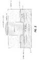
- FIG. 2 is a sectional view of the device wafer of FIG. 1, but with an additional resist layer having a plated stud therethrough.[0012]
- FIG. 3[0013]ais a sectional view of the combination of device wafer and stud of FIG. 2 but with the resist removed. And the copper stud is fully passivated with a barrier layer, noble metal layer and a solderable joining layer.
- FIG. 3[0014]bis a sectional view of the combination of the device wafer and the stud after capping of the stud tips with a barrier metal, noble metal and a joining metal layer.
- FIG. 4 is a sectional view of the combination of device wafer and stud of FIG. 3[0015]b, but with the wafer aligned to a carrier with socket or receptacle in the carrier having appropriate contiguous metal layers.
- Referring now to the Figures of the drawing, the device wafer process will first be described with several options or embodiments. Then, the carrier process flow is described to complete the structure being formed.[0016]
- Above the last level of[0017]
interconnect wiring layer 16 on the device chip wafers, atop passivation stack 12 dielectric layer is applied and contact holes, serving to house receptacles orsockets 14, are formed to provide access to the contact sites on the last metal level. Then, TaN/Ta layer 18 andCu layer 20 are deposited on top of the structure and the copper is removed from the top surface of the carrier by CMP, stopping on the Ta. This results inCu 20 being present only at the bottom and side walls of the receptacles, as shown in FIG. 1. A photoresist layer22 (FIG. 2) is applied and patterned to have openings coincident with the contact holes. The size of these openings can be equal to or greater than the diameter of the contact holes. The thickness of the resist is chosen in accordance with the final height desired for thecopper stud 24. A metal such as Cu is electroplated through the openings using the copper seed in the contact holes as the seeding area. After slight overplating to ensure all openings in the resist are filled, CMP of the Cu is done, stopping on the resist. As a result, thecopper studs 24 with a predetermined height are realized. - At this point, the process can continue in different ways to produce slightly different end structures:[0018]
- Option 1: Copper stud fully coated with a barrier layer[0019]
- Strip resist, electroplate Ni, immersion Au (plating occurs only on Cu studs since Ta surface does not plate readily); electroplate solder or tin and etch TaNTa from the area between studs by wet or dry methods.[0020]
- OR[0021]
- Strip resist, deposit electroless Ni—P, immersion Au (plating occurs only on Cu since the electroless and immersion steps are selective for Cu), electroplate solder or Sn and etch TaN, Ta from the area between the studs by wet or dry methods, resulting in a structure shown in FIG. 3[0022]a.
- OR[0023]
- Strip resist, etch TaN Ta, electroless Ni—P, immersion Au and Sn (same as above)[0024]
- One can use an optional electroless CoWP layer as an added diffusion barrier between Cu and Ni if that is required.[0025]
- Option 2: Copper stud capped only at the tips with a barrier layer[0026]
- Electroplate Ni, immersion Au, electroplate solder or tin. Strip resist and etch TaN, Ta.[0027]
- OR[0028]
- Electroless Ni—P, immersion Au, electroplate solder or Sn. Strip resist and etch TaNTa.[0029]
- This structure is desired if the joining materials need to be confined to the stud tip only, and the resulting structure is shown in FIG. 3[0030]b.
- Alternate methods, or portions of the process flow, may be employed which are described in dockets FIS920000015US1 (Replated Metal Structures . . . ) and FIS919990197US1 (Pattern-Sensitive Electrolytic Metal Plating). In these methods the formation of the pads desired on the upper surface is determined by the presence or absence of metal features in the layers that lie underneath the intralevel dielectric due to electric field perturbations. This is a limitation in that the top layer pattern cannot be generated independent of the pattern of the underlying metal levels. Other films such as Ti, W, TiN, WN, Cr or combinations thereof can be substituted for Ta and TaN, and Ni can be replaced by Co, Pt or Pd.[0031]
- The carrier process flow comprises:[0032]
- 1. Start with a silicon, ceramic, or organic carrier with interchip wiring as well as wiring and contacts to connect to external electronics. The wiring may have multiple levels and the carrier may have vias through it to allow for connections to the back.[0033]
- 2. Form vias in the upper dielectric layer where contacts to the device chips will be made.[0034]
- 3. Deposit a liner/seed layer such as TaN—Ta (about 40 μm) and Cu (about 100 μm).[0035]
- 4. CMP off the Cu from the surface and stop on Ta. Cu is left in the bottom of the contact depressions and their side walls.[0036]
- 5. Electroplate a barrier layer such as 0.5 micron of Ni into the contact openings using a process that plates only on Cu. The TaN—Ta layer serves to bring in the current, but no plating takes place on it.[0037]
- 6. Electroplate a noble metal such as thin Au (about 0.1 micron) or apply immersion Au on the Ni surface. The latter may be simpler and more controlled in thickness (800 to 1200A). The former leads to an all electroplated sequence. Also, the immersion Au solution, which usually contains cyanide, can be replaced by an electroless Au, non-cyanide bath which is very selective to Ni and which can be deposited in a very short time (2 minutes) rather than having to expose the piece for 30 minutes in immersion Au.[0038]
- 7. Etch the TaN—Ta layer by a wet or dry etch process. Other metals such as Ti, W, TiN, WN, Cr or combinations thereof can be substituted for Ta and TaN, and Ni can be replaced by Co, Pt or Pd.[0039]
- The assembly involves a pick and place process of the chiplets in a manner similar to the regular flip chips (split optics and/or capacitance aligned) followed by reflow joining. A hydrogen reflow without flux may be preferred when the gap between the chiplet and the carrier is too small for efficient flux cleaning.[0040]
- Some of the unique advantages of the resulting structure are:[0041]
- 1. The use of chip processing techniques for the device chips as well as the carrier allows a very high density of interconnects down to a 10-micron pitch. This is a much higher density than is possible with conventional chip to carrier joining. Higher density down to a 2.5-micron pitch is feasible if required.[0042]
- 2. The structure can be tailored to have a high stand off height to accommodate variations in the planarity of the carrier substrate.[0043]
- 3. The height of the interconnects can be selected to reduce thermal mismatch related shear strains in the microjoints since these strains scale inversely with the joint height.[0044]
- 4. Taller microjoints can also be used to create an adequate separation between the chip and the carrier so that a suitable underfill material can be injected and cured in the gap. This is required if the thermal expansion mismatch between the chip and the carrier is large and the chip size is large (typically 10 mm on edge or more). The underfill acts as a reinforcement and reduces the stresses experienced by the joints.[0045]
- 5. The flexibility in choosing the height can also be used to ensure that the back surfaces of the flip mounted collection of devices are reasonably coplanar even when the joining pads may have different heights in different chips (e.g., large flip chip solder in one chip versus ultra high pitch microjoints in another, the stud height can be used to equate the joint heights in both cases). This coplanarity is important if a common surface for heat removal is needed on the back of the chips as in the case of the heat sink attachment to a high performance processor system.[0046]
- 6. The joining metallurgy on the stud tips can be Pb-based solder, Pb-free solder or AuSn alloy. In the latter two cases, the joint will be free of alpha particle issues related to the solder since there is no lead in the joints close to the device chips.[0047]
- The invention having been thus described with particular reference to the preferred forms thereof, it will be obvious that various changes and modifications may be made therein without departing from the spirit and scope of the invention as defined in the appended claims.[0048]
Claims (15)
Priority Applications (3)
| Application Number | Priority Date | Filing Date | Title |
|---|---|---|---|
| US10/052,591US6732908B2 (en) | 2002-01-18 | 2002-01-18 | High density raised stud microjoining system and methods of fabricating the same |
| JP2003003619AJP3782997B2 (en) | 2002-01-18 | 2003-01-09 | System and method for connecting device chips |
| TW092100835ATWI222168B (en) | 2002-01-18 | 2003-01-16 | High density raised stud microjoining system and methods of fabricating the same |
Applications Claiming Priority (1)
| Application Number | Priority Date | Filing Date | Title |
|---|---|---|---|
| US10/052,591US6732908B2 (en) | 2002-01-18 | 2002-01-18 | High density raised stud microjoining system and methods of fabricating the same |
Publications (2)
| Publication Number | Publication Date |
|---|---|
| US20030136814A1true US20030136814A1 (en) | 2003-07-24 |
| US6732908B2 US6732908B2 (en) | 2004-05-11 |
Family
ID=21978593
Family Applications (1)
| Application Number | Title | Priority Date | Filing Date |
|---|---|---|---|
| US10/052,591Expired - LifetimeUS6732908B2 (en) | 2002-01-18 | 2002-01-18 | High density raised stud microjoining system and methods of fabricating the same |
Country Status (3)
| Country | Link |
|---|---|
| US (1) | US6732908B2 (en) |
| JP (1) | JP3782997B2 (en) |
| TW (1) | TWI222168B (en) |
Cited By (12)
| Publication number | Priority date | Publication date | Assignee | Title |
|---|---|---|---|---|
| WO2003060960A3 (en)* | 2002-01-18 | 2004-04-15 | Ibm | High density area array solder microjoining interconnect structure and fabrication method |
| US6732908B2 (en)* | 2002-01-18 | 2004-05-11 | International Business Machines Corporation | High density raised stud microjoining system and methods of fabricating the same |
| US20070232049A1 (en)* | 2006-04-04 | 2007-10-04 | International Business Machines Corporation | Method and structure for eliminating aluminum terminal pad material in semiconductor devices |
| US20080235941A1 (en)* | 2007-03-30 | 2008-10-02 | Seng Guan Chow | Integrated circuit package system with mounting features |
| WO2008100923A3 (en)* | 2007-02-12 | 2008-11-06 | Ibm | Undercut-free blm process for pb-free and pb-reduced c4 |
| WO2009048738A1 (en)* | 2007-10-11 | 2009-04-16 | Maxim Integrated Products, Inc. | Bump i/o contact for semiconductor device |
| US20090095502A1 (en)* | 2007-10-11 | 2009-04-16 | International Business Machines Corporation | Multilayer pillar for reduced stress interconnect and method of making same |
| US20110084387A1 (en)* | 2003-09-22 | 2011-04-14 | Dubin Valery M | Designs and methods for conductive bumps |
| US8643424B2 (en) | 2006-03-21 | 2014-02-04 | Maxim Integrated Products, Inc. | Passive offset and overshoot cancellation for sampled-data circuits |
| US20190341376A1 (en)* | 2014-01-17 | 2019-11-07 | Taiwan Semiconductor Manufacturing Company, Ltd. | Integrated Circuit Package and Methods of Forming Same |
| CN110854085A (en)* | 2019-11-22 | 2020-02-28 | 江苏中科智芯集成科技有限公司 | Chip packaging structure and packaging method |
| US11444015B2 (en)* | 2018-02-26 | 2022-09-13 | Tdk Corporation | Electronic device with stud bumps |
Families Citing this family (14)
| Publication number | Priority date | Publication date | Assignee | Title |
|---|---|---|---|---|
| TWI245402B (en)* | 2002-01-07 | 2005-12-11 | Megic Corp | Rod soldering structure and manufacturing process thereof |
| WO2004093505A2 (en)* | 2003-04-15 | 2004-10-28 | Wavezero, Inc. | Emi shielding for electronic component packaging |
| JP2008547205A (en)* | 2005-06-14 | 2008-12-25 | キュービック・ウエハ・インコーポレーテッド | Chip connector |
| US7989958B2 (en) | 2005-06-14 | 2011-08-02 | Cufer Assett Ltd. L.L.C. | Patterned contact |
| US7863183B2 (en)* | 2006-01-18 | 2011-01-04 | International Business Machines Corporation | Method for fabricating last level copper-to-C4 connection with interfacial cap structure |
| US20070284420A1 (en)* | 2006-06-13 | 2007-12-13 | Advanpack Solutions Pte Ltd | Integrated circuit chip formed on substrate |
| US20080277778A1 (en) | 2007-05-10 | 2008-11-13 | Furman Bruce K | Layer Transfer Process and Functionally Enhanced Integrated Circuits Products Thereby |
| US20090279275A1 (en)* | 2008-05-09 | 2009-11-12 | Stephen Peter Ayotte | Method of attaching an integrated circuit chip to a module |
| JP5277788B2 (en)* | 2008-08-14 | 2013-08-28 | ソニー株式会社 | Semiconductor device and manufacturing method thereof |
| TWI473221B (en)* | 2008-09-05 | 2015-02-11 | Unimicron Technology Corp | Package substrate and fabrication method thereof |
| EP2273545B1 (en)* | 2009-07-08 | 2016-08-31 | Imec | Method for insertion bonding and kit of parts for use in said method |
| TWI450349B (en)* | 2010-08-31 | 2014-08-21 | Global Unichip Corp | Method for detecting the under-fill void in flip chip bga |
| JP5870493B2 (en)* | 2011-02-24 | 2016-03-01 | セイコーエプソン株式会社 | Semiconductor devices, sensors and electronic devices |
| WO2015195082A1 (en)* | 2014-06-16 | 2015-12-23 | Intel Corporation | Method for direct integration of memory die to logic die without use of through silicon vias (tsv) |
Citations (13)
| Publication number | Priority date | Publication date | Assignee | Title |
|---|---|---|---|---|
| US3458925A (en)* | 1966-01-20 | 1969-08-05 | Ibm | Method of forming solder mounds on substrates |
| US3942245A (en)* | 1971-11-20 | 1976-03-09 | Ferranti Limited | Related to the manufacture of lead frames and the mounting of semiconductor devices thereon |
| US4413308A (en)* | 1981-08-31 | 1983-11-01 | Bell Telephone Laboratories, Incorporated | Printed wiring board construction |
| US5348214A (en)* | 1990-11-20 | 1994-09-20 | Sumitomo Electric Industries, Ltd. | Method of mounting semiconductor elements |
| US5668405A (en)* | 1994-09-14 | 1997-09-16 | Nec Corporation | Semiconductor device with a film carrier tape |
| US6020561A (en)* | 1996-03-29 | 2000-02-01 | Intel Corporation | Printed circuit substrate with solder formed on pad-on-via and pad-off-via contacts thereof |
| US6107180A (en)* | 1998-01-30 | 2000-08-22 | Motorola, Inc. | Method for forming interconnect bumps on a semiconductor die |
| US6153490A (en)* | 1997-07-01 | 2000-11-28 | Texas Instruments Incorporated | Method for forming integrated circuit capacitor and memory |
| US6180881B1 (en)* | 1998-05-05 | 2001-01-30 | Harlan Ruben Isaak | Chip stack and method of making same |
| US6358832B1 (en)* | 1999-09-30 | 2002-03-19 | International Business Machines Corporation | Method of forming barrier layers for damascene interconnects |
| US6476463B1 (en)* | 1998-05-28 | 2002-11-05 | Nec Corporation | Microwave integrated circuit multi-chip-module |
| US6525275B1 (en)* | 1996-08-05 | 2003-02-25 | Ibiden Co., Ltd. | Multilayer printed circuit boards |
| US6534863B2 (en)* | 2001-02-09 | 2003-03-18 | International Business Machines Corporation | Common ball-limiting metallurgy for I/O sites |
Family Cites Families (12)
| Publication number | Priority date | Publication date | Assignee | Title |
|---|---|---|---|---|
| JPS63175450A (en)* | 1987-01-16 | 1988-07-19 | Hitachi Ltd | Hermetically sealed semiconductor device |
| DE4446471C2 (en)* | 1994-12-23 | 1997-05-22 | Fraunhofer Ges Forschung | Method for mounting a chip on a flexible circuit carrier |
| DE19830159A1 (en)* | 1998-07-06 | 2000-01-20 | Siemens Ag | Chip-module with high density interconnect wiring substrate carrier |
| US6344125B1 (en) | 2000-04-06 | 2002-02-05 | International Business Machines Corporation | Pattern-sensitive electrolytic metal plating |
| US6368484B1 (en) | 2000-05-09 | 2002-04-09 | International Business Machines Corporation | Selective plating process |
| US6339024B1 (en) | 2000-06-28 | 2002-01-15 | International Business Machines Corporation | Reinforced integrated circuits |
| WO2002004704A2 (en)* | 2000-07-11 | 2002-01-17 | Applied Materials, Inc. | Method and apparatus for patching electrochemically deposited layers using electroless deposited materials |
| US6927471B2 (en)* | 2001-09-07 | 2005-08-09 | Peter C. Salmon | Electronic system modules and method of fabrication |
| US20030122206A1 (en)* | 2001-11-09 | 2003-07-03 | Amal Bhattarai | Multi-chip module integrating MEMS mirror array with electronics |
| US6732908B2 (en)* | 2002-01-18 | 2004-05-11 | International Business Machines Corporation | High density raised stud microjoining system and methods of fabricating the same |
| US6661098B2 (en)* | 2002-01-18 | 2003-12-09 | International Business Machines Corporation | High density area array solder microjoining interconnect structure and fabrication method |
| US6747472B2 (en)* | 2002-01-18 | 2004-06-08 | International Business Machines Corporation | Temporary device attach structure for test and burn in of microjoint interconnects and method for fabricating the same |
- 2002
- 2002-01-18USUS10/052,591patent/US6732908B2/ennot_activeExpired - Lifetime
- 2003
- 2003-01-09JPJP2003003619Apatent/JP3782997B2/ennot_activeExpired - Fee Related
- 2003-01-16TWTW092100835Apatent/TWI222168B/ennot_activeIP Right Cessation
Patent Citations (13)
| Publication number | Priority date | Publication date | Assignee | Title |
|---|---|---|---|---|
| US3458925A (en)* | 1966-01-20 | 1969-08-05 | Ibm | Method of forming solder mounds on substrates |
| US3942245A (en)* | 1971-11-20 | 1976-03-09 | Ferranti Limited | Related to the manufacture of lead frames and the mounting of semiconductor devices thereon |
| US4413308A (en)* | 1981-08-31 | 1983-11-01 | Bell Telephone Laboratories, Incorporated | Printed wiring board construction |
| US5348214A (en)* | 1990-11-20 | 1994-09-20 | Sumitomo Electric Industries, Ltd. | Method of mounting semiconductor elements |
| US5668405A (en)* | 1994-09-14 | 1997-09-16 | Nec Corporation | Semiconductor device with a film carrier tape |
| US6020561A (en)* | 1996-03-29 | 2000-02-01 | Intel Corporation | Printed circuit substrate with solder formed on pad-on-via and pad-off-via contacts thereof |
| US6525275B1 (en)* | 1996-08-05 | 2003-02-25 | Ibiden Co., Ltd. | Multilayer printed circuit boards |
| US6153490A (en)* | 1997-07-01 | 2000-11-28 | Texas Instruments Incorporated | Method for forming integrated circuit capacitor and memory |
| US6107180A (en)* | 1998-01-30 | 2000-08-22 | Motorola, Inc. | Method for forming interconnect bumps on a semiconductor die |
| US6180881B1 (en)* | 1998-05-05 | 2001-01-30 | Harlan Ruben Isaak | Chip stack and method of making same |
| US6476463B1 (en)* | 1998-05-28 | 2002-11-05 | Nec Corporation | Microwave integrated circuit multi-chip-module |
| US6358832B1 (en)* | 1999-09-30 | 2002-03-19 | International Business Machines Corporation | Method of forming barrier layers for damascene interconnects |
| US6534863B2 (en)* | 2001-02-09 | 2003-03-18 | International Business Machines Corporation | Common ball-limiting metallurgy for I/O sites |
Cited By (33)
| Publication number | Priority date | Publication date | Assignee | Title |
|---|---|---|---|---|
| WO2003060960A3 (en)* | 2002-01-18 | 2004-04-15 | Ibm | High density area array solder microjoining interconnect structure and fabrication method |
| US6732908B2 (en)* | 2002-01-18 | 2004-05-11 | International Business Machines Corporation | High density raised stud microjoining system and methods of fabricating the same |
| US20110084387A1 (en)* | 2003-09-22 | 2011-04-14 | Dubin Valery M | Designs and methods for conductive bumps |
| US11201129B2 (en) | 2003-09-22 | 2021-12-14 | Intel Corporation | Designs and methods for conductive bumps |
| US10249588B2 (en) | 2003-09-22 | 2019-04-02 | Intel Corporation | Designs and methods for conductive bumps |
| US9543261B2 (en) | 2003-09-22 | 2017-01-10 | Intel Corporation | Designs and methods for conductive bumps |
| JP2015167257A (en)* | 2003-09-22 | 2015-09-24 | インテル コーポレイション | Small electronic device, method of forming the same, and system |
| JP2013138260A (en)* | 2003-09-22 | 2013-07-11 | Intel Corp | Compact electronic apparatus, formation method thereof, and system |
| US8643424B2 (en) | 2006-03-21 | 2014-02-04 | Maxim Integrated Products, Inc. | Passive offset and overshoot cancellation for sampled-data circuits |
| US8912838B1 (en) | 2006-03-21 | 2014-12-16 | Maxim Integrated Products, Inc. | Passive offset and overshoot cancellation for sampled data circuits |
| US7375021B2 (en) | 2006-04-04 | 2008-05-20 | International Business Machines Corporation | Method and structure for eliminating aluminum terminal pad material in semiconductor devices |
| US20070232049A1 (en)* | 2006-04-04 | 2007-10-04 | International Business Machines Corporation | Method and structure for eliminating aluminum terminal pad material in semiconductor devices |
| WO2008100923A3 (en)* | 2007-02-12 | 2008-11-06 | Ibm | Undercut-free blm process for pb-free and pb-reduced c4 |
| US20080235941A1 (en)* | 2007-03-30 | 2008-10-02 | Seng Guan Chow | Integrated circuit package system with mounting features |
| US9084377B2 (en)* | 2007-03-30 | 2015-07-14 | Stats Chippac Ltd. | Integrated circuit package system with mounting features for clearance |
| US9111816B2 (en) | 2007-10-11 | 2015-08-18 | International Business Machines Corporation | Multilayer pillar for reduced stress interconnect and method of making same |
| US10403590B2 (en) | 2007-10-11 | 2019-09-03 | International Business Machines Corporation | Multilayer pillar for reduced stress interconnect and method of making same |
| US8269345B2 (en) | 2007-10-11 | 2012-09-18 | Maxim Integrated Products, Inc. | Bump I/O contact for semiconductor device |
| US9368466B2 (en) | 2007-10-11 | 2016-06-14 | Maxim Integrated Products, Inc. | Bump I/O contact for semiconductor device |
| US9472520B2 (en) | 2007-10-11 | 2016-10-18 | International Business Machines Corporation | Multilayer pillar for reduced stress interconnect and method of making same |
| US20090095502A1 (en)* | 2007-10-11 | 2009-04-16 | International Business Machines Corporation | Multilayer pillar for reduced stress interconnect and method of making same |
| US9640501B2 (en) | 2007-10-11 | 2017-05-02 | International Business Machines Corporation | Multilayer pillar for reduced stress interconnect and method of making same |
| US20090096092A1 (en)* | 2007-10-11 | 2009-04-16 | Patel Pradip D | Bump I/O Contact for Semiconductor Device |
| US10396051B2 (en) | 2007-10-11 | 2019-08-27 | International Business Machines Corporation | Multilayer pillar for reduced stress interconnect and method of making same |
| US8293587B2 (en)* | 2007-10-11 | 2012-10-23 | International Business Machines Corporation | Multilayer pillar for reduced stress interconnect and method of making same |
| US11244917B2 (en) | 2007-10-11 | 2022-02-08 | International Business Machines Corporation | Multilayer pillar for reduced stress interconnect and method of making same |
| WO2009048738A1 (en)* | 2007-10-11 | 2009-04-16 | Maxim Integrated Products, Inc. | Bump i/o contact for semiconductor device |
| US11094657B2 (en) | 2007-10-11 | 2021-08-17 | International Business Machines Corporation | Multilayer pillar for reduced stress interconnect and method of making same |
| US11171102B2 (en) | 2007-10-11 | 2021-11-09 | International Business Machines Corporation | Multilayer pillar for reduced stress interconnect and method of making same |
| US11152344B2 (en)* | 2014-01-17 | 2021-10-19 | Taiwan Semiconductor Manufacturing Company, Ltd. | Integrated circuit package and methods of forming same |
| US20190341376A1 (en)* | 2014-01-17 | 2019-11-07 | Taiwan Semiconductor Manufacturing Company, Ltd. | Integrated Circuit Package and Methods of Forming Same |
| US11444015B2 (en)* | 2018-02-26 | 2022-09-13 | Tdk Corporation | Electronic device with stud bumps |
| CN110854085A (en)* | 2019-11-22 | 2020-02-28 | 江苏中科智芯集成科技有限公司 | Chip packaging structure and packaging method |
Also Published As
| Publication number | Publication date |
|---|---|
| TW200400591A (en) | 2004-01-01 |
| TWI222168B (en) | 2004-10-11 |
| JP2003273158A (en) | 2003-09-26 |
| JP3782997B2 (en) | 2006-06-07 |
| US6732908B2 (en) | 2004-05-11 |
Similar Documents
| Publication | Publication Date | Title |
|---|---|---|
| US6732908B2 (en) | High density raised stud microjoining system and methods of fabricating the same | |
| US6661098B2 (en) | High density area array solder microjoining interconnect structure and fabrication method | |
| US11201129B2 (en) | Designs and methods for conductive bumps | |
| US8018069B2 (en) | Through-hole contacts in a semiconductor device | |
| JP3663405B2 (en) | System for testing a device chip and method for testing a device chip | |
| US11282716B2 (en) | Integration structure and planar joining | |
| HK1093380B (en) | Microelectronic apparatus including conductive bumps and method thereof |
Legal Events
| Date | Code | Title | Description |
|---|---|---|---|
| AS | Assignment | Owner name:INTERNATIONAL BUSINESS MACHINES CORPORATION, NEW Y Free format text:ASSIGNMENT OF ASSIGNORS INTEREST;ASSIGNORS:FURMAN, BRUCE KENNETH;SURENDRA, MAHESWARAN;GOMA, SHERIF A.;AND OTHERS;REEL/FRAME:012527/0886;SIGNING DATES FROM 20011221 TO 20020110 | |
| FEPP | Fee payment procedure | Free format text:PAYOR NUMBER ASSIGNED (ORIGINAL EVENT CODE: ASPN); ENTITY STATUS OF PATENT OWNER: LARGE ENTITY | |
| STCF | Information on status: patent grant | Free format text:PATENTED CASE | |
| FPAY | Fee payment | Year of fee payment:4 | |
| FPAY | Fee payment | Year of fee payment:8 | |
| AS | Assignment | Owner name:ULTRATECH, INC., CALIFORNIA Free format text:ASSIGNMENT OF ASSIGNORS INTEREST;ASSIGNOR:INTERNATIONAL BUSINESS MACHINES CORPORATION;REEL/FRAME:028959/0001 Effective date:20120718 | |
| FEPP | Fee payment procedure | Free format text:PAT HOLDER NO LONGER CLAIMS SMALL ENTITY STATUS, ENTITY STATUS SET TO UNDISCOUNTED (ORIGINAL EVENT CODE: STOL); ENTITY STATUS OF PATENT OWNER: LARGE ENTITY | |
| REFU | Refund | Free format text:REFUND - PAYMENT OF MAINTENANCE FEE, 12TH YR, SMALL ENTITY (ORIGINAL EVENT CODE: R2553); ENTITY STATUS OF PATENT OWNER: LARGE ENTITY | |
| FEPP | Fee payment procedure | Free format text:PAT HOLDER CLAIMS SMALL ENTITY STATUS, ENTITY STATUS SET TO SMALL (ORIGINAL EVENT CODE: LTOS); ENTITY STATUS OF PATENT OWNER: LARGE ENTITY | |
| FPAY | Fee payment | Year of fee payment:12 | |
| AS | Assignment | Owner name:VEECO INSTRUMENTS INC., NEW YORK Free format text:ASSIGNMENT OF ASSIGNORS INTEREST;ASSIGNOR:ULTRATECH, INC.;REEL/FRAME:051446/0476 Effective date:20191219 | |
| AS | Assignment | Owner name:HSBC BANK USA, NATIONAL ASSOCIATION, AS COLLATERAL AGENT, NEW YORK Free format text:PATENT SECURITY AGREEMENT;ASSIGNOR:VEECO INSTRUMENTS INC.;REEL/FRAME:058533/0321 Effective date:20211216 | |
| AS | Assignment | Owner name:HSBC BANK USA, NATIONAL ASSOCIATION, NEW YORK Free format text:SECURITY INTEREST;ASSIGNOR:VEECO INSTRUMENTS INC.;REEL/FRAME:071649/0225 Effective date:20250616 |