US20030135829A1 - Methodology of creating an object database from a Gerber file - Google Patents
Methodology of creating an object database from a Gerber fileDownload PDFInfo
- Publication number
- US20030135829A1 US20030135829A1US10/186,228US18622802AUS2003135829A1US 20030135829 A1US20030135829 A1US 20030135829A1US 18622802 AUS18622802 AUS 18622802AUS 2003135829 A1US2003135829 A1US 2003135829A1
- Authority
- US
- United States
- Prior art keywords
- data
- printed circuit
- circuit board
- active element
- data set
- Prior art date
- Legal status (The legal status is an assumption and is not a legal conclusion. Google has not performed a legal analysis and makes no representation as to the accuracy of the status listed.)
- Granted
Links
Images


Classifications
- G—PHYSICS
- G06—COMPUTING OR CALCULATING; COUNTING
- G06F—ELECTRIC DIGITAL DATA PROCESSING
- G06F30/00—Computer-aided design [CAD]
- G06F30/30—Circuit design
- G06F30/39—Circuit design at the physical level
Definitions
- This applicationrelates generally to an apparatus and method for converting data describing the layout of a printed circuit board into a format recognizable by vision software, and more particularly to an apparatus and method for converting data describing the layout of a printed circuit board into a format recognizable by a printed circuit board inspection system.
- Printed circuit boardsare used to link various electrical components into a single compact and operable unit.
- the boardsconsist generally of a substrate upon which alternating layers of conductive shapes (such as pads or paths) and dielectric material are printed.
- the dielectric layersare used to electrically isolate one conductive layer of the printed circuit board from another conductive layer, except where electrical connection is desired (e.g., a via may permit electrical communication from one conductive layer of a printed circuit board to another layer).
- CADcomputer aided design
- Gerber data formatA Gerber data file describes the layout of a layer of a printed circuit board by containing coordinates describing where a shape is to be printed, what geometry the shape should take on, and where the shape should end.
- the Gerber data formatdescribes complex geometries as the intersection of simple geometries. This scheme is depicted in FIG. 1.
- FIG. 1depicts a magnified view of a small portion of a printed circuit board.
- the portion depicted in FIG. 1contains eight pads 100 - 114 arranged in a generally rectangular fashion, as might be used for connection to a simple integrated circuit containing eight pins.
- each of the pads 100 - 114has an elongated body with a rounded top and a rounded bottom. Rather than represent pad geometry as a single data element, per the Gerber data format, each pad would be represented as the intersection of three separate simple shapes, as shown by the blow-up of pad 114 .
- each pad 100 - 114is actually defined as the intersection of a circle 116 (forming the top of the pad), a rectangle 118 (forming the body of the pad), and another circle 120 (forming the bottom of the pad).
- the Gerber data defining a printed circuit boardmay be passed to an inspection system that examines each layer of the printed circuit board to determine if it has been etched correctly.
- an inspection system that makes use of Gerber datamust make several passes over a complex geometry in order to determine that the geometry is correctly printed. For example, with respect to the pads 100 - 114 depicted in FIG. 1, an inspection device operating based upon Gerber data would have to make three passes for each pad 100 - 114 : a first pass to look for the top circle 116 , a second pass to look for the rectangular body 118 , and a third pass to look for the bottom circle 120 . This sort of redundancy reduces the overall efficiency of the inspection system. This same issue presents itself when inspecting solder paste printing quality during printed circuit board assembly.
- Gerber dataAnother consequence of passing Gerber data to an inspection system is that the inspection system will perform its operations in the sequence defined by the Gerber file. This means that the inspection system may examine a first geometry located in one position, and then inspect a second geometry located on the other side of the board, rather than inspecting a geometry located next to the last-inspected geometry. Such a scheme is inefficient, and reduces the overall through-put of the inspection system. This same issue presents itself when inspecting solder paste printing quality during printed circuit board assembly.
- Gerber datamay be translated into a format readable by vision software (such as may be found on a printed circuit board inspection system).
- a desirable solutionmay represent complex geometries as a single data element. Additionally, a desirable solution may order its translated data format in such a way as to prevent the inspection system from consecutively inspecting geometries situated in non-proximate regions of the board.
- a method of converting a data set describing a layout of a printed circuit board into a format recognizable by vision softwaremay be realized by finding a first data element representing a first shape that intersects with a second shape represented by a second data element. Next, the first and second data elements are merged. Finally, the merged element is exported as a single data element.
- a computerized system for converting a data set describing a layout of a printed circuit board into a format recognizable by vision softwaremay include a memory element that stores the data set describing the layout of the printed circuit board.
- a processormay be operably coupled to the memory element. The processor may be programmed to perform the following steps. First, a first data element representing a first shape that intersects with a second shape represented by a second data element is found. Then, the first and second data elements are merged. Finally, the merged element is exported as a single data element.
- a system for converting a data set describing a layout of a printed circuit board into a format recognizable by vision softwaremay include a memory element storing the data set describing the layout of the printed circuit board. Additionally, the system may include a means for merging data elements representing overlapping shapes.
- FIG. 1depicts a portion of a printed circuit board that includes geometries described by the intersection of simple geometries.
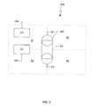
- FIG. 2depicts systems in which the schemes disclosed herein may be deployed.
- FIG. 3depicts a portion of a printed circuit board divided into four virtual regions, each of which contains shapes represented by data elements.
- FIG. 4depicts a complex shape bounded by a bounding rectangle.
- FIG. 5depicts an operation flow, in accordance with one embodiment of the present invention.
- FIG. 6depicts a printed circuit board divided into a plurality of virtual regions. The elements within each region are input into a data file on a region-by-region basis to produce an orderly inspection.
- a Gerber data filemay be translated into a data format usable by vision software through a process whereby a first Gerber data element is selected and is examined to determine if the shape represented by that element intersects with any other shapes. Each shape intersecting the selected element is merged into a single data object with the selected element. This process is repeated for each element describing the printed circuit board layout. The consequence of this procedure is that complex geometries that had been represented as the intersection of many simple geometries are represented as individual data objects.
- the above-described processmay be streamlined by organizing the printed circuit board into virtual regions. According to such a scheme, it is first determined in which region or regions the selected element is situated. Thus, only those regions must be searched for shapes intersecting the shape represented by the selected element. The process of searching for intersecting shapes is repeated for each data element in each region.
- the passages related to FIGS. 3 - 5disclose a scheme for organizing the converted data so as to permitan inspection system to progress in an orderly fashion as it examines a printed circuit board (rather than progressing in a haphazard, random fashion).
- the passage related to FIG. 2discloses the various systems in which the methods discussed with reference to FIGS. 3 - 6 may be embodied.
- FIG. 2depicts a CAD system 200 , and inspection system 202 , and a conversion system 204 , each of which is connected by a network 206
- the methods disclosed hereinmay be embodied in software running on the CAD system 200 the inspection system 202 , or any third computer system, such as a dedicated conversion system 204 . Additionally, the methods disclosed herein are susceptible of deployment in any computing system.
- the methods disclosed hereinmay be used to receive data emanating from the CAD system 200 , convert such data (known as Gerber data), and export such data in a format readable by the inspection system 202 .
- the inspection system 202is able to inspect the printed circuit board described by the converted data.
- Inspection systemssuch as 202
- CAD systemssuch as 200
- the inspection procedure performed by the inspection system 202may include inspecting the printed circuit board for proper etching or for proper solder paste printing quality.
- FIG. 3depicts a portion of a printed circuit board 300 .
- the portion of the circuit board 300 depicted in FIG. 3contains three shapes 302 , 304 , and 306 .
- shape 302is represented, in a Gerber file, by elements E 1 , E 4 , and E 5 .
- Shapes 304 and 306are represented by elements E 2 and E 3 , respectively.
- the procedure disclosed hereinfinds complex shapes composed of multiple intersecting shapes, and represents those shapes in a single data object (as opposed to being represented by multiple Gerber elements).
- shape 302when operated upon by the procedure disclosed herein, shape 302 will be represented by a single data object, rather than by Gerber elements E 1 , E 4 , and E 5 .
- Gerber elements E 1 , E 4 , and E 5when operated upon by the procedure disclosed herein, shape 302 will be represented by a single data object, rather than by Gerber elements E 1 , E 4 , and E 5 .
- simultaneous referencewill be made to the flowchart depicted in FIG. 5 and to the hypothetical portion of the printed circuit board 300 depicted in FIG. 3.
- the conversion procedurebegins by receiving Gerber data from the CAD system 200 , as shown in FIG. 5 by operation 500 .
- the Gerber datamay be transferred to the machine executing the conversion method by any manner (it may be transferred via a network 206 , via a diskette (not pictured), via inter-task messaging, etc.).
- the procedurebegins by dividing the printed circuit board 300 into a plurality of virtual regions, as shown by operation 502 . As depicted by FIG. 3, the printed circuit board 300 has been divided into four virtual regions B 1 , B 2 , B 3 , and B 4 , which are rectangular shaped blocks that tessellate with one another.
- the virtual regions B 1 , B 2 , B 3 , and B 4limit the scope of the search for intersecting shapes. Accordingly, the size, shape, and number of virtual regions into which a printed circuit board is divided is a design choice that influences the processing time required to execute the conversion method.
- a link list of each of the Gerber elementsis created, as shown by operation 504 .
- elements E 1 -E 5are entered into a link list.
- the link listwould initially appear as follows:
- the link liststores a list of all Gerber elements that have not been examined to determine if the shapes they represent intersect with another shape. Thereafter, as shown by operation 506 , a first element is selected from the link list; this element is termed the “active element.”
- the active elementis an element that is examined to determine if the shape it represents intersects with the shapes represented by the other elements in the link list. For the sake of illustration, assume that element E 1 (which represents the circle forming the top portion of the pad 302 ) is selected as the active element in operation 506 Next, as shown in operation 508 , the active element E 1 is removed from the link list, meaning the link list appears as follows:
- the active element E 1After the active element E 1 has been removed from the link list, it is determined in which virtual regions the active element E 1 is situated. In this case, the active element E 1 is situated in regions B 1 and B 2 Per operation 510 , one of the regions in which the active element E 1 is situated is chosen as an inspection region. Let us assume region B 1 is chosen.
- an element from region B 1is selected.
- element E 4which is situated partially in region B 1 , is selected.
- operation 514it is determined whether or not the selected element E 4 intersects the active element E 1 . In this case, the two elements do in fact intersect, thus control is turned over to operation 516 .
- the selected element E 4 and the active element E 1are merged, which means that they are associated by a link, and the selected element E 4 is removed from the link list, meaning the link list appears as follows:
- elements E 2 and E 3are each at least partially situated within the inspection region, so control returns to operation 512 , whereupon one of the two elements E 2 or E 3 will be selected for inspection to determine whether they intersect with the active element, which is the merger of E 1 and E 4
- a loopis constructed which is traversed twice (once for inspection of E 2 and once for the inspection of E 3 ), during which it is determined that neither E 2 nor E 3 intersect with the active element.
- controlis passed from query operation 518 (where it is determined that there are no more elements to examine in region B 1 ) to query operation 520 In query operation 520 , it is determined whether or not there are more blocks in which the active element (merged E 1 and E 4 ) is situated. In this case, the answer is in the affirmative, because the active element lies in regions B 3 , B 4 , and B 2 —none of which have yet been inspected. Therefore, control is passed to operation 510 , in which another region containing the active element is chosen for inspection. Let us assume region B 3 is selected next.
- region B 3is inspected for shapes intersecting the active element, as opposed to region B 1 being the inspection region.
- region B 3is inspected for shapes intersecting the active element, as opposed to region B 1 being the inspection region.
- element E 5intersects the active element (which is the merger of E 1 and E 4 ).
- element E 5is merged with the active element (in operation 516 ), which means that it is associated with the active element by a link, and is removed from the link list.
- the link listappears as follows:
- the methodwill continue to traverse the above-described loops searching for: (1) additional elements in the selected inspection block (this loop is defined by operations 512 , 514 , 516 , and 518 ); and (2) additional blocks in which the active element lies (this loop is defined by operations 510 , 512 , 514 , 516 , 518 , and 520 ).
- this loopis defined by operations 510 , 512 , 514 , 516 , 518 , and 520 .
- the merged elementmay be exported as a single data object.
- the format of the exported data objectwill vary based upon the system to which the data object is to be exported.
- a typical formatincludes a data object having three fields: (1) a description of a bounding rectangle (an example of which is identified by reference numeral 400 in FIG. 4) of the complex geometry; (2) shape of the object; and (3) size of the object as compared to the bounding rectangle 400 .
- FIG. 6depicts a printed circuit board 600 that has been divided into ninety-nine virtual regions.
- One scheme for ordering a converted data fileis to order the file so as to have elements representing shapes within a particular corner region 602 of the circuit board 600 be listed at the top of the file. Next, elements representing shapes contained in the virtual region above the corner region 602 are listed in the file.
- the filegoes on to list elements representing shapes contained in virtual regions, based upon a region-by-region scheme, wherein each successive region is chosen to be located directly above the last region, until the top 604 of the board is encountered. When the top 604 of the board is encountered, the shapes in the adjacent region 606 are next listed.
- the patterncontinues in a generally zigzag pattern, as depicted in FIG. 6, until the elements representing each shape are entered into the output file. Consequently, the inspection system, which progresses in the same order as the elements are listed in the file, will inspect the board 600 in an orderly fashion.
- a method of converting a data set describing a layout of a printed circuit board into a format recognizable by vision softwarecan be accomplished by finding a first data element representing a first shape that intersects with a second shape represented by a second data element (such as is accomplished by operations 502 - 514 ) Next the first and second data elements are merged (such as is shown by operation 516 ). Finally, the merged element is exported as a single data element (such as in operation 522 ). The exported data element may be exported to an inspection system, which may use the data to perform its inspection functions. This method is especially suited for operation upon a Gerber data set. The Gerber data may be received from a printed circuit board computer aided design system (as is shown by operation 500 ).
- the methodmay involve other steps, such as dividing a layer of the printed circuit board into a plurality of regions (such as in operation 502 ). For example, a layer of the printed circuit board may be divided into a plurality of rectangular, tessellating regions.
- a data elementmay be identified as an active element (such as in operation 506 ).
- a region in which the shape represented by the active element is situatedmay be identified (such as in operation 510 ).
- all other shapes intersecting the shape represented by the active elementmay be found (such as is shown by operations 512 , 514 , 516 , and 518 ).
- those elementsmay be merged with the active element, (such as in operation 516 ). Thereafter, the merged data element is identified as the active element (such as in operation 516 ). Next, another region in which the shape represented by the active element is situated may be identified (such as is shown in operation 520 ). Then, within the aforementioned region, all other shapes intersecting the shape represented by the active element may be found (such as is shown by operations 510 , 512 , 514 , 516 , 518 and 520 ). Finally, the intersecting element may be merged (such as is shown in operation 516 ). The above-describe steps may be repeated until all regions in which the shape represented by the active element is situated have been identified.
- a computing apparatus(such as 200 , 202 , or 204 ), which contains a processor and a memory element, may be programmed to implement the above-describe methods.
- a printed circuit boardmay be divided into virtual regions of any shape and in any number.
- other methods of ordering the converted data file to produce an orderly, efficient inspectionmay be utilized.
- the filemay be ordered so that each successive element in the file is chosen so that it represents a shape that is the shortest distance from the shape represented by the preceding element.
- other hardware arrangementsmay be used to implement the data conversion methods disclosed herein. Numerous other changes may be made which will readily suggest themselves to those skilled in the art and which are encompassed in the invention disclosed and as defined in the appended claims.
Landscapes
- Engineering & Computer Science (AREA)
- Computer Hardware Design (AREA)
- Physics & Mathematics (AREA)
- Theoretical Computer Science (AREA)
- Evolutionary Computation (AREA)
- Geometry (AREA)
- General Engineering & Computer Science (AREA)
- General Physics & Mathematics (AREA)
- Investigating Materials By The Use Of Optical Means Adapted For Particular Applications (AREA)
- Design And Manufacture Of Integrated Circuits (AREA)
Abstract
Description
- This application claims priority of U.S. provisional application Serial No. 60/350,134, filed Jan. 17, 2002 and entitled “METHODOLOGY OF CREATING OBJECT DATABASE FROM GERBER FILE.”[0001]
- This application relates generally to an apparatus and method for converting data describing the layout of a printed circuit board into a format recognizable by vision software, and more particularly to an apparatus and method for converting data describing the layout of a printed circuit board into a format recognizable by a printed circuit board inspection system.[0002]
- Printed circuit boards are used to link various electrical components into a single compact and operable unit. The boards consist generally of a substrate upon which alternating layers of conductive shapes (such as pads or paths) and dielectric material are printed. The dielectric layers are used to electrically isolate one conductive layer of the printed circuit board from another conductive layer, except where electrical connection is desired (e.g., a via may permit electrical communication from one conductive layer of a printed circuit board to another layer).[0003]
- Typically, a computer aided design (CAD) system is used to design printed circuit boards. Generally, CAD systems represent the design of printed circuit boards in a data format known as the Gerber data format. A Gerber data file describes the layout of a layer of a printed circuit board by containing coordinates describing where a shape is to be printed, what geometry the shape should take on, and where the shape should end. Notably, the Gerber data format describes complex geometries as the intersection of simple geometries. This scheme is depicted in FIG. 1.[0004]
- FIG. 1 depicts a magnified view of a small portion of a printed circuit board. The portion depicted in FIG. 1 contains eight pads[0005]100-114 arranged in a generally rectangular fashion, as might be used for connection to a simple integrated circuit containing eight pins. As can be seen from FIG. 1, each of the pads100-114 has an elongated body with a rounded top and a rounded bottom. Rather than represent pad geometry as a single data element, per the Gerber data format, each pad would be represented as the intersection of three separate simple shapes, as shown by the blow-up of
pad 114. As can be seen from the blown-up depiction ofpad 114, each pad100-114 is actually defined as the intersection of a circle116 (forming the top of the pad), a rectangle118 (forming the body of the pad), and another circle120 (forming the bottom of the pad). - In the course of manufacturing printed circuit boards, the Gerber data defining a printed circuit board may be passed to an inspection system that examines each layer of the printed circuit board to determine if it has been etched correctly. One repercussion of representing complex geometries as the intersection of simple geometries is that an inspection system that makes use of Gerber data must make several passes over a complex geometry in order to determine that the geometry is correctly printed. For example, with respect to the pads[0006]100-114 depicted in FIG. 1, an inspection device operating based upon Gerber data would have to make three passes for each pad100-114: a first pass to look for the
top circle 116, a second pass to look for therectangular body 118, and a third pass to look for thebottom circle 120. This sort of redundancy reduces the overall efficiency of the inspection system. This same issue presents itself when inspecting solder paste printing quality during printed circuit board assembly. - Another consequence of passing Gerber data to an inspection system is that the inspection system will perform its operations in the sequence defined by the Gerber file. This means that the inspection system may examine a first geometry located in one position, and then inspect a second geometry located on the other side of the board, rather than inspecting a geometry located next to the last-inspected geometry. Such a scheme is inefficient, and reduces the overall through-put of the inspection system. This same issue presents itself when inspecting solder paste printing quality during printed circuit board assembly.[0007]
- As is evident from the foregoing discussion, there exists a need for a scheme by which Gerber data may be translated into a format readable by vision software (such as may be found on a printed circuit board inspection system). A desirable solution may represent complex geometries as a single data element. Additionally, a desirable solution may order its translated data format in such a way as to prevent the inspection system from consecutively inspecting geometries situated in non-proximate regions of the board.[0008]
- Against this backdrop the present embodiments have been developed. A method of converting a data set describing a layout of a printed circuit board into a format recognizable by vision software may be realized by finding a first data element representing a first shape that intersects with a second shape represented by a second data element. Next, the first and second data elements are merged. Finally, the merged element is exported as a single data element.[0009]
- According to another embodiment of the invention, a computerized system for converting a data set describing a layout of a printed circuit board into a format recognizable by vision software may include a memory element that stores the data set describing the layout of the printed circuit board. A processor may be operably coupled to the memory element. The processor may be programmed to perform the following steps. First, a first data element representing a first shape that intersects with a second shape represented by a second data element is found. Then, the first and second data elements are merged. Finally, the merged element is exported as a single data element.[0010]
- According to yet another embodiment of the invention, a system for converting a data set describing a layout of a printed circuit board into a format recognizable by vision software may include a memory element storing the data set describing the layout of the printed circuit board. Additionally, the system may include a means for merging data elements representing overlapping shapes.[0011]
- These and various other features as well as advantages which characterize the present invention will be apparent from a reading of the following detailed description and a review of the associated drawings.[0012]
- FIG. 1 depicts a portion of a printed circuit board that includes geometries described by the intersection of simple geometries.[0013]
- FIG. 2 depicts systems in which the schemes disclosed herein may be deployed.[0014]
- FIG. 3 depicts a portion of a printed circuit board divided into four virtual regions, each of which contains shapes represented by data elements.[0015]
- FIG. 4 depicts a complex shape bounded by a bounding rectangle.[0016]
- FIG. 5 depicts an operation flow, in accordance with one embodiment of the present invention.[0017]
- FIG. 6 depicts a printed circuit board divided into a plurality of virtual regions. The elements within each region are input into a data file on a region-by-region basis to produce an orderly inspection.[0018]
- A Gerber data file may be translated into a data format usable by vision software through a process whereby a first Gerber data element is selected and is examined to determine if the shape represented by that element intersects with any other shapes. Each shape intersecting the selected element is merged into a single data object with the selected element. This process is repeated for each element describing the printed circuit board layout. The consequence of this procedure is that complex geometries that had been represented as the intersection of many simple geometries are represented as individual data objects.[0019]
- The above-described process may be streamlined by organizing the printed circuit board into virtual regions. According to such a scheme, it is first determined in which region or regions the selected element is situated. Thus, only those regions must be searched for shapes intersecting the shape represented by the selected element. The process of searching for intersecting shapes is repeated for each data element in each region.[0020]
- A detailed discussion of the scheme for converting Gerber data into data usable by vision software is found in the passages related to FIGS.[0021]3-5. The passages related to FIG. 6 disclose a scheme for organizing the converted data so as to permitan inspection system to progress in an orderly fashion as it examines a printed circuit board (rather than progressing in a haphazard, random fashion). The passage related to FIG. 2 discloses the various systems in which the methods discussed with reference to FIGS.3-6 may be embodied.
- FIG. 2 depicts a[0022]
CAD system 200, andinspection system 202, and aconversion system 204, each of which is connected by anetwork 206 The methods disclosed herein may be embodied in software running on theCAD system 200 theinspection system 202, or any third computer system, such as adedicated conversion system 204. Additionally, the methods disclosed herein are susceptible of deployment in any computing system. - In practice, the methods disclosed herein may be used to receive data emanating from the[0023]
CAD system 200, convert such data (known as Gerber data), and export such data in a format readable by theinspection system 202. Thus, by virtue of receiving the converted data, theinspection system 202 is able to inspect the printed circuit board described by the converted data. Inspection systems (such as202) and CAD systems (such as200) are well known in the art, and require no discussion regarding the particulars of their construction. It is observed, however, that theCAD system 200, theinspection system 202, and theconversion system 204 each contain hardware typical of a computing environment (i.e., a processor, a memory element in cooperation with the processor, etc.). The inspection procedure performed by theinspection system 202 may include inspecting the printed circuit board for proper etching or for proper solder paste printing quality. - FIG. 3 depicts a portion of a printed[0024]
circuit board 300. The portion of thecircuit board 300 depicted in FIG. 3 contains threeshapes shape 302 is represented, in a Gerber file, by elements E1, E4, and E5.Shapes - As stated earlier, the procedure disclosed herein finds complex shapes composed of multiple intersecting shapes, and represents those shapes in a single data object (as opposed to being represented by multiple Gerber elements). For example, when operated upon by the procedure disclosed herein,[0025]
shape 302 will be represented by a single data object, rather than by Gerber elements E1, E4, and E5. During discussion of the procedure, simultaneous reference will be made to the flowchart depicted in FIG. 5 and to the hypothetical portion of the printedcircuit board 300 depicted in FIG. 3. - Optionally, the conversion procedure begins by receiving Gerber data from the[0026]
CAD system 200, as shown in FIG. 5 byoperation 500. The Gerber data may be transferred to the machine executing the conversion method by any manner (it may be transferred via anetwork 206, via a diskette (not pictured), via inter-task messaging, etc.). Initially, the procedure begins by dividing the printedcircuit board 300 into a plurality of virtual regions, as shown byoperation 502. As depicted by FIG. 3, the printedcircuit board 300 has been divided into four virtual regions B1, B2, B3, and B4, which are rectangular shaped blocks that tessellate with one another. As will become evident below, the virtual regions B1, B2, B3, and B4 limit the scope of the search for intersecting shapes. Accordingly, the size, shape, and number of virtual regions into which a printed circuit board is divided is a design choice that influences the processing time required to execute the conversion method. - After creation of the virtual regions, a link list of each of the Gerber elements is created, as shown by[0027]
operation 504. Thus, with reference to the exemplary printedcircuit board portion 300, elements E1-E5 are entered into a link list. Thus, the link list would initially appear as follows: - E1→E2→E3→E4→E5
- The link list stores a list of all Gerber elements that have not been examined to determine if the shapes they represent intersect with another shape. Thereafter, as shown by[0028]
operation 506, a first element is selected from the link list; this element is termed the “active element.” The active element is an element that is examined to determine if the shape it represents intersects with the shapes represented by the other elements in the link list. For the sake of illustration, assume that element E1 (which represents the circle forming the top portion of the pad302) is selected as the active element inoperation 506 Next, as shown inoperation 508, the active element E1 is removed from the link list, meaning the link list appears as follows: - E2→E3→E4→E5
- After the active element E[0029]1 has been removed from the link list, it is determined in which virtual regions the active element E1 is situated. In this case, the active element E1 is situated in regions B1 and
B2 Per operation 510, one of the regions in which the active element E1 is situated is chosen as an inspection region. Let us assume region B1 is chosen. - Thereafter, in[0030]
operation 512, an element from region B1 is selected. Let us assume element E4, which is situated partially in region B1, is selected. Inoperation 514 it is determined whether or not the selected element E4 intersects the active element E1. In this case, the two elements do in fact intersect, thus control is turned over tooperation 516. - In[0031]
operation 516, the selected element E4 and the active element E1 are merged, which means that they are associated by a link, and the selected element E4 is removed from the link list, meaning the link list appears as follows: - E2→E3→E5
- Control flows to query[0032]
operation 518, in which it is determined whether there are additional elements in the inspection region B1. In this case, elements E2 and E3 are each at least partially situated within the inspection region, so control returns tooperation 512, whereupon one of the two elements E2 or E3 will be selected for inspection to determine whether they intersect with the active element, which is the merger of E1 and E4 By virtue ofoperations - After the inspection of elements E[0033]2 and E3, control is passed from query operation518 (where it is determined that there are no more elements to examine in region B1) to query
operation 520 Inquery operation 520, it is determined whether or not there are more blocks in which the active element (merged E1 and E4) is situated. In this case, the answer is in the affirmative, because the active element lies in regions B3, B4, and B2—none of which have yet been inspected. Therefore, control is passed tooperation 510, in which another region containing the active element is chosen for inspection. Let us assume region B3 is selected next. - After selection of region B[0034]3 in
operation 510, the flow of operation progresses as described previously with reference to operations512-518, with the sole exception being that region B3 is inspected for shapes intersecting the active element, as opposed to region B1 being the inspection region. As a consequence of inspecting region B3, it is found that the shape represented by element E5 intersects the active element (which is the merger of E1 and E4). Thus, element E5 is merged with the active element (in operation516), which means that it is associated with the active element by a link, and is removed from the link list. Thus, the link list appears as follows: - E2→E3
- After merging element E[0035]5 with the active element in
operation 516, the method will continue to traverse the above-described loops searching for: (1) additional elements in the selected inspection block (this loop is defined byoperations operations - Finally, in[0036]
operation 522, the merged element may be exported as a single data object. The format of the exported data object will vary based upon the system to which the data object is to be exported. A typical format, however, includes a data object having three fields: (1) a description of a bounding rectangle (an example of which is identified byreference numeral 400 in FIG. 4) of the complex geometry; (2) shape of the object; and (3) size of the object as compared to the boundingrectangle 400. - As discussed previously, another optional aspect of the scheme disclosed herein is to produce a converted data format that is not only usable by an inspection system, but is also ordered so as to allow the inspection system to proceed through a printed circuit board in an orderly manner. FIG. 6 depicts a printed[0037]
circuit board 600 that has been divided into ninety-nine virtual regions. One scheme for ordering a converted data file (such as would result from use of the method depicted in FIG. 5), is to order the file so as to have elements representing shapes within aparticular corner region 602 of thecircuit board 600 be listed at the top of the file. Next, elements representing shapes contained in the virtual region above thecorner region 602 are listed in the file. The file goes on to list elements representing shapes contained in virtual regions, based upon a region-by-region scheme, wherein each successive region is chosen to be located directly above the last region, until the top604 of the board is encountered. When the top604 of the board is encountered, the shapes in theadjacent region 606 are next listed. The pattern continues in a generally zigzag pattern, as depicted in FIG. 6, until the elements representing each shape are entered into the output file. Consequently, the inspection system, which progresses in the same order as the elements are listed in the file, will inspect theboard 600 in an orderly fashion. - To summarize, a method of converting a data set describing a layout of a printed circuit board into a format recognizable by vision software can be accomplished by finding a first data element representing a first shape that intersects with a second shape represented by a second data element (such as is accomplished by operations[0038]502-514) Next the first and second data elements are merged (such as is shown by operation516). Finally, the merged element is exported as a single data element (such as in operation522). The exported data element may be exported to an inspection system, which may use the data to perform its inspection functions. This method is especially suited for operation upon a Gerber data set. The Gerber data may be received from a printed circuit board computer aided design system (as is shown by operation500).
- The method may involve other steps, such as dividing a layer of the printed circuit board into a plurality of regions (such as in operation[0039]502). For example, a layer of the printed circuit board may be divided into a plurality of rectangular, tessellating regions. Next, a data element may be identified as an active element (such as in operation506). Thereafter, a region in which the shape represented by the active element is situated may be identified (such as in operation510). Finally, within the identified region, all other shapes intersecting the shape represented by the active element may be found (such as is shown by
operations - Upon identification of intersecting shapes within an inspection region, those elements may be merged with the active element, (such as in operation[0040]516). Thereafter, the merged data element is identified as the active element (such as in operation516). Next, another region in which the shape represented by the active element is situated may be identified (such as is shown in operation520). Then, within the aforementioned region, all other shapes intersecting the shape represented by the active element may be found (such as is shown by
operations - A computing apparatus (such as[0041]200,202, or204), which contains a processor and a memory element, may be programmed to implement the above-describe methods.
- It will be clear that the present invention is well adapted to attain the ends and advantages mentioned as well as those inherent therein. While a presently preferred embodiment has been described for purposes of this disclosure, various changes and modifications may be made which are well within the scope of the present invention. For example, a printed circuit board may be divided into virtual regions of any shape and in any number. Additionally, other methods of ordering the converted data file to produce an orderly, efficient inspection may be utilized. For example, the file may be ordered so that each successive element in the file is chosen so that it represents a shape that is the shortest distance from the shape represented by the preceding element. Furthermore, other hardware arrangements may be used to implement the data conversion methods disclosed herein. Numerous other changes may be made which will readily suggest themselves to those skilled in the art and which are encompassed in the invention disclosed and as defined in the appended claims.[0042]
Claims (22)
Priority Applications (2)
| Application Number | Priority Date | Filing Date | Title |
|---|---|---|---|
| US10/186,228US6920624B2 (en) | 2002-01-17 | 2002-06-28 | Methodology of creating an object database from a Gerber file |
| PCT/US2003/020586WO2004015595A2 (en) | 2002-06-28 | 2003-06-27 | Methodology of creating an object database from a gerber file |
Applications Claiming Priority (2)
| Application Number | Priority Date | Filing Date | Title |
|---|---|---|---|
| US35013402P | 2002-01-17 | 2002-01-17 | |
| US10/186,228US6920624B2 (en) | 2002-01-17 | 2002-06-28 | Methodology of creating an object database from a Gerber file |
Publications (2)
| Publication Number | Publication Date |
|---|---|
| US20030135829A1true US20030135829A1 (en) | 2003-07-17 |
| US6920624B2 US6920624B2 (en) | 2005-07-19 |
Family
ID=31714173
Family Applications (1)
| Application Number | Title | Priority Date | Filing Date |
|---|---|---|---|
| US10/186,228Expired - Fee RelatedUS6920624B2 (en) | 2002-01-17 | 2002-06-28 | Methodology of creating an object database from a Gerber file |
Country Status (2)
| Country | Link |
|---|---|
| US (1) | US6920624B2 (en) |
| WO (1) | WO2004015595A2 (en) |
Cited By (5)
| Publication number | Priority date | Publication date | Assignee | Title |
|---|---|---|---|---|
| US20040088660A1 (en)* | 2002-10-30 | 2004-05-06 | Trung Tran | Method and system for searching a microelectronic device physical layout |
| WO2006095892A1 (en)* | 2005-03-08 | 2006-09-14 | Fujifilm Corporation | Image processing method, image processor, drawing system, and program |
| US20070011232A1 (en)* | 2005-07-06 | 2007-01-11 | Microsoft Corporation | User interface for starting presentations in a meeting |
| US7536665B1 (en)* | 2006-07-25 | 2009-05-19 | Cadence Design Systems, Inc. | User-guided autorouting |
| US7793249B1 (en) | 2006-07-25 | 2010-09-07 | Cadence Design Systems, Inc. | Method and system for adaptive bundling of connections in user-guided autorouting |
Families Citing this family (10)
| Publication number | Priority date | Publication date | Assignee | Title |
|---|---|---|---|---|
| EP1754398A4 (en)* | 2004-05-15 | 2010-03-24 | Stablcor Inc | Printed wiring board with conductive constraining core including resin filled channels |
| JP2006235762A (en)* | 2005-02-22 | 2006-09-07 | Orion Denki Kk | Cad system for printed circuit board |
| EP1862040A4 (en)* | 2005-03-15 | 2009-11-04 | Stablcore Inc | Manufacturing process: how to construct constraining core material into printed wiring board |
| USRE45637E1 (en) | 2005-08-29 | 2015-07-28 | Stablcor Technology, Inc. | Processes for manufacturing printed wiring boards |
| US7730613B2 (en)* | 2005-08-29 | 2010-06-08 | Stablcor, Inc. | Processes for manufacturing printed wiring boards |
| US8203080B2 (en)* | 2006-07-14 | 2012-06-19 | Stablcor Technology, Inc. | Build-up printed wiring board substrate having a core layer that is part of a circuit |
| WO2008045900A1 (en)* | 2006-10-09 | 2008-04-17 | Mentor Graphics Corporation | Properties in electronic design automation |
| US9323880B2 (en) | 2014-05-28 | 2016-04-26 | GE Intelligent Platforms, Inc | Apparatus and method for file translation |
| US9332632B2 (en) | 2014-08-20 | 2016-05-03 | Stablcor Technology, Inc. | Graphene-based thermal management cores and systems and methods for constructing printed wiring boards |
| CN106227946B (en)* | 2016-07-26 | 2019-03-12 | 上海望友信息科技有限公司 | A kind of PCB web plate production method and system |
Citations (30)
| Publication number | Priority date | Publication date | Assignee | Title |
|---|---|---|---|---|
| US5157762A (en)* | 1990-04-10 | 1992-10-20 | Gerber Systems Corporation | Method and apparatus for providing a three state data base for use with automatic optical inspection systems |
| US5163128A (en)* | 1990-07-27 | 1992-11-10 | Gerber Systems Corporation | Method and apparatus for generating a multiple tolerance, three state data base for use with automatic optical inspection systems |
| US5513099A (en)* | 1993-02-08 | 1996-04-30 | Probot Incorporated | Circuit board repair and rework apparatus |
| US5515293A (en)* | 1993-12-22 | 1996-05-07 | Vlsi Technology, Inc. | Method and apparatus for generating a linked data structure for integrated circuit layout |
| US5608453A (en)* | 1993-10-26 | 1997-03-04 | Gerber Systems Corporation | Automatic optical inspection system having a weighted transition database |
| US5691913A (en)* | 1994-03-28 | 1997-11-25 | Matsushita Electric Ind. Co. | Layout designing apparatus for circuit boards |
| US5856925A (en)* | 1993-09-27 | 1999-01-05 | Fujitsu Limited | Method for making electronic circuit design data and CAD system using the method |
| US5862973A (en)* | 1997-01-30 | 1999-01-26 | Teradyne, Inc. | Method for inspecting solder paste in printed circuit board manufacture |
| US5912984A (en)* | 1996-12-19 | 1999-06-15 | Cognex Corporation | Method and apparatus for in-line solder paste inspection |
| US5982927A (en)* | 1996-12-19 | 1999-11-09 | Cognex Corporation | Methods and apparatuses for in-line solder paste inspection |
| US6091996A (en)* | 1998-03-02 | 2000-07-18 | Electronic Packaging Company | Printed circuit board analysis and repair system |
| USD446796S1 (en)* | 2000-10-05 | 2001-08-21 | Cyberoptics Corporation | Solder paste inspection machine |
| US6317513B2 (en)* | 1996-12-19 | 2001-11-13 | Cognex Corporation | Method and apparatus for inspecting solder paste using geometric constraints |
| US6477266B1 (en)* | 1998-12-11 | 2002-11-05 | Lucent Technologies Inc. | Vision comparison inspection system graphical user interface |
| US6483937B1 (en)* | 1999-06-17 | 2002-11-19 | International Business Machines Corporation | Process for inspecting an object |
| US6493858B2 (en)* | 2001-03-23 | 2002-12-10 | The Board Of Trustees Of The Leland Stanford Jr. University | Method and system for displaying VLSI layout data |
| US6496270B1 (en)* | 2000-02-17 | 2002-12-17 | Gsi Lumonics, Inc. | Method and system for automatically generating reference height data for use in a three-dimensional inspection system |
| US6516452B2 (en)* | 2001-05-01 | 2003-02-04 | Chipdata, Inc. | Method and apparatus for verifying design data |
| US6631508B1 (en)* | 2000-06-07 | 2003-10-07 | Xilinx, Inc. | Method and apparatus for developing and placing a circuit design |
| US6678874B1 (en)* | 2001-11-28 | 2004-01-13 | Unisys Corporation | Computer-aided design (CAD) tool |
| US6701003B1 (en)* | 2000-04-10 | 2004-03-02 | Innoventions, Inc. | Component identification system for electronic board testers |
| US6714671B1 (en)* | 1999-06-02 | 2004-03-30 | Matsushita Electric Industrial Co., Ltd. | Method of detecting pattern defects |
| US6738503B1 (en)* | 1999-08-27 | 2004-05-18 | Renesas Technology Corp. | Notch inspection apparatus and method based on shading pattern matching |
| US6738958B2 (en)* | 2001-09-10 | 2004-05-18 | Numerical Technologies, Inc. | Modifying a hierarchical representation of a circuit to process composite gates |
| US6757421B1 (en)* | 2000-09-27 | 2004-06-29 | Cognex Corporation | Method and apparatus for detecting defects |
| US6760890B2 (en)* | 2001-11-29 | 2004-07-06 | Agilent Technologies, Inc. | Systems and methods for linking a graphical display and an n-dimensional data structure in a graphical user interface |
| US6760471B1 (en)* | 2000-06-23 | 2004-07-06 | Teradyne, Inc. | Compensation system and related techniques for use in a printed circuit board inspection system |
| US6771805B1 (en)* | 1999-10-06 | 2004-08-03 | Keiso Research Laboratories, Inc. | Perspective viewing inspection system |
| US6771807B2 (en)* | 2000-01-18 | 2004-08-03 | Solvision Inc. | Method and system for detecting defects on a printed circuit board |
| US6788806B2 (en)* | 2000-01-12 | 2004-09-07 | Fuji Machine Manufacturing Company | Board-supporting inspecting method |
Family Cites Families (1)
| Publication number | Priority date | Publication date | Assignee | Title |
|---|---|---|---|---|
| JP3634447B2 (en)* | 1995-07-14 | 2005-03-30 | キヤノン株式会社 | Image processing apparatus and method |
- 2002
- 2002-06-28USUS10/186,228patent/US6920624B2/ennot_activeExpired - Fee Related
- 2003
- 2003-06-27WOPCT/US2003/020586patent/WO2004015595A2/ennot_activeApplication Discontinuation
Patent Citations (30)
| Publication number | Priority date | Publication date | Assignee | Title |
|---|---|---|---|---|
| US5157762A (en)* | 1990-04-10 | 1992-10-20 | Gerber Systems Corporation | Method and apparatus for providing a three state data base for use with automatic optical inspection systems |
| US5163128A (en)* | 1990-07-27 | 1992-11-10 | Gerber Systems Corporation | Method and apparatus for generating a multiple tolerance, three state data base for use with automatic optical inspection systems |
| US5513099A (en)* | 1993-02-08 | 1996-04-30 | Probot Incorporated | Circuit board repair and rework apparatus |
| US5856925A (en)* | 1993-09-27 | 1999-01-05 | Fujitsu Limited | Method for making electronic circuit design data and CAD system using the method |
| US5608453A (en)* | 1993-10-26 | 1997-03-04 | Gerber Systems Corporation | Automatic optical inspection system having a weighted transition database |
| US5515293A (en)* | 1993-12-22 | 1996-05-07 | Vlsi Technology, Inc. | Method and apparatus for generating a linked data structure for integrated circuit layout |
| US5691913A (en)* | 1994-03-28 | 1997-11-25 | Matsushita Electric Ind. Co. | Layout designing apparatus for circuit boards |
| US5912984A (en)* | 1996-12-19 | 1999-06-15 | Cognex Corporation | Method and apparatus for in-line solder paste inspection |
| US5982927A (en)* | 1996-12-19 | 1999-11-09 | Cognex Corporation | Methods and apparatuses for in-line solder paste inspection |
| US6317513B2 (en)* | 1996-12-19 | 2001-11-13 | Cognex Corporation | Method and apparatus for inspecting solder paste using geometric constraints |
| US5862973A (en)* | 1997-01-30 | 1999-01-26 | Teradyne, Inc. | Method for inspecting solder paste in printed circuit board manufacture |
| US6091996A (en)* | 1998-03-02 | 2000-07-18 | Electronic Packaging Company | Printed circuit board analysis and repair system |
| US6477266B1 (en)* | 1998-12-11 | 2002-11-05 | Lucent Technologies Inc. | Vision comparison inspection system graphical user interface |
| US6714671B1 (en)* | 1999-06-02 | 2004-03-30 | Matsushita Electric Industrial Co., Ltd. | Method of detecting pattern defects |
| US6483937B1 (en)* | 1999-06-17 | 2002-11-19 | International Business Machines Corporation | Process for inspecting an object |
| US6738503B1 (en)* | 1999-08-27 | 2004-05-18 | Renesas Technology Corp. | Notch inspection apparatus and method based on shading pattern matching |
| US6771805B1 (en)* | 1999-10-06 | 2004-08-03 | Keiso Research Laboratories, Inc. | Perspective viewing inspection system |
| US6788806B2 (en)* | 2000-01-12 | 2004-09-07 | Fuji Machine Manufacturing Company | Board-supporting inspecting method |
| US6771807B2 (en)* | 2000-01-18 | 2004-08-03 | Solvision Inc. | Method and system for detecting defects on a printed circuit board |
| US6496270B1 (en)* | 2000-02-17 | 2002-12-17 | Gsi Lumonics, Inc. | Method and system for automatically generating reference height data for use in a three-dimensional inspection system |
| US6701003B1 (en)* | 2000-04-10 | 2004-03-02 | Innoventions, Inc. | Component identification system for electronic board testers |
| US6631508B1 (en)* | 2000-06-07 | 2003-10-07 | Xilinx, Inc. | Method and apparatus for developing and placing a circuit design |
| US6760471B1 (en)* | 2000-06-23 | 2004-07-06 | Teradyne, Inc. | Compensation system and related techniques for use in a printed circuit board inspection system |
| US6757421B1 (en)* | 2000-09-27 | 2004-06-29 | Cognex Corporation | Method and apparatus for detecting defects |
| USD446796S1 (en)* | 2000-10-05 | 2001-08-21 | Cyberoptics Corporation | Solder paste inspection machine |
| US6493858B2 (en)* | 2001-03-23 | 2002-12-10 | The Board Of Trustees Of The Leland Stanford Jr. University | Method and system for displaying VLSI layout data |
| US6516452B2 (en)* | 2001-05-01 | 2003-02-04 | Chipdata, Inc. | Method and apparatus for verifying design data |
| US6738958B2 (en)* | 2001-09-10 | 2004-05-18 | Numerical Technologies, Inc. | Modifying a hierarchical representation of a circuit to process composite gates |
| US6678874B1 (en)* | 2001-11-28 | 2004-01-13 | Unisys Corporation | Computer-aided design (CAD) tool |
| US6760890B2 (en)* | 2001-11-29 | 2004-07-06 | Agilent Technologies, Inc. | Systems and methods for linking a graphical display and an n-dimensional data structure in a graphical user interface |
Cited By (7)
| Publication number | Priority date | Publication date | Assignee | Title |
|---|---|---|---|---|
| US20040088660A1 (en)* | 2002-10-30 | 2004-05-06 | Trung Tran | Method and system for searching a microelectronic device physical layout |
| US6763502B2 (en)* | 2002-10-30 | 2004-07-13 | Sun Microsystems, Inc. | Method and system for searching a microelectronic device physical layout |
| WO2006095892A1 (en)* | 2005-03-08 | 2006-09-14 | Fujifilm Corporation | Image processing method, image processor, drawing system, and program |
| US20080304767A1 (en)* | 2005-03-08 | 2008-12-11 | Fujifilm Corporation | Image Processing Method, Image Processor, Drawing System, and Program |
| US20070011232A1 (en)* | 2005-07-06 | 2007-01-11 | Microsoft Corporation | User interface for starting presentations in a meeting |
| US7536665B1 (en)* | 2006-07-25 | 2009-05-19 | Cadence Design Systems, Inc. | User-guided autorouting |
| US7793249B1 (en) | 2006-07-25 | 2010-09-07 | Cadence Design Systems, Inc. | Method and system for adaptive bundling of connections in user-guided autorouting |
Also Published As
| Publication number | Publication date |
|---|---|
| WO2004015595A2 (en) | 2004-02-19 |
| WO2004015595A3 (en) | 2004-04-01 |
| US6920624B2 (en) | 2005-07-19 |
Similar Documents
| Publication | Publication Date | Title |
|---|---|---|
| US6920624B2 (en) | Methodology of creating an object database from a Gerber file | |
| US5987240A (en) | Design rules checker for an integrated circuit design | |
| US5550714A (en) | Schematic generator and schematic generating method | |
| US5644500A (en) | Routing program generating method and apparatus therefor, placement program generating method and apparatus therefor, and automatic routing method and apparatus therefor | |
| US8196080B2 (en) | Method and system for routing | |
| US7499045B2 (en) | Graphics image generation | |
| US5124273A (en) | Automatic wiring method for semiconductor integrated circuit devices | |
| Case et al. | Solid logic design automation | |
| US5933349A (en) | Component placement | |
| Tsai et al. | NEWS: A net-even-wiring system for the routing on a multilayer PGA package | |
| Marek-Sadowska et al. | The crossing distribution problem [IC layout] | |
| JP2805538B2 (en) | Printed wiring board connection verification device | |
| Jaja et al. | On routing two-terminal nets in the presence of obstacles | |
| Anway et al. | PLINT layout system for VLSI chips | |
| JP3166847B2 (en) | Recording medium and device recording wiring accommodation evaluation program in printed circuit board design | |
| EP0654745A2 (en) | Graphical display system for routing and repartitioning circuits during layout | |
| US3683416A (en) | Process for generating representations of packages of logic elements utilizing a data processing machine | |
| Brown et al. | Design automation and the WRAP System | |
| Ginsberg et al. | An updated multilayer printed wiring CAD capability | |
| Protsko et al. | Mondrian: system for automatic generation of dataflow diagrams | |
| JPH0721239A (en) | Design rule check execution device | |
| JPH09283629A (en) | Method of arranging logic element of semiconductor integrated circuit | |
| EP0715267A2 (en) | Routing method and apparatus | |
| JPH05258015A (en) | Printed circuit board cam data calculating device | |
| Farlow | Machine aids to the design of ceramic substrates containing integrated circuit chips |
Legal Events
| Date | Code | Title | Description |
|---|---|---|---|
| AS | Assignment | Owner name:SEAGATE TECHNOLOGY LLC, CALIFORNIA Free format text:ASSIGNMENT OF ASSIGNORS INTEREST;ASSIGNORS:GARREPALLY, SRINIVAS;TONG, SIM CHING;SOWMITHRI, CHANNASUMUDRAM KRISHNAMURTHY;AND OTHERS;REEL/FRAME:013297/0099;SIGNING DATES FROM 20020626 TO 20020701 | |
| AS | Assignment | Owner name:JPMORGAN CHASE BANK, AS COLLATERAL AGENT, NEW YORK Free format text:SECURITY INTEREST;ASSIGNOR:SEAGATE TECHNOLOGY LLC;REEL/FRAME:013516/0015 Effective date:20020513 | |
| FEPP | Fee payment procedure | Free format text:PAYER NUMBER DE-ASSIGNED (ORIGINAL EVENT CODE: RMPN); ENTITY STATUS OF PATENT OWNER: LARGE ENTITY Free format text:PAYOR NUMBER ASSIGNED (ORIGINAL EVENT CODE: ASPN); ENTITY STATUS OF PATENT OWNER: LARGE ENTITY | |
| AS | Assignment | Owner name:SEAGATE TECHNOLOGY LLC, CALIFORNIA Free format text:RELEASE OF SECURITY INTERESTS IN PATENT RIGHTS;ASSIGNOR:JPMORGAN CHASE BANK, N.A. (FORMERLY KNOWN AS THE CHASE MANHATTAN BANK AND JPMORGAN CHASE BANK), AS ADMINISTRATIVE AGENT;REEL/FRAME:016967/0001 Effective date:20051130 | |
| FPAY | Fee payment | Year of fee payment:4 | |
| AS | Assignment | Owner name:WELLS FARGO BANK, NATIONAL ASSOCIATION, AS COLLATERAL AGENT AND SECOND PRIORITY REPRESENTATIVE, CALIFORNIA Free format text:SECURITY AGREEMENT;ASSIGNORS:MAXTOR CORPORATION;SEAGATE TECHNOLOGY LLC;SEAGATE TECHNOLOGY INTERNATIONAL;REEL/FRAME:022757/0017 Effective date:20090507 Owner name:JPMORGAN CHASE BANK, N.A., AS ADMINISTRATIVE AGENT AND FIRST PRIORITY REPRESENTATIVE, NEW YORK Free format text:SECURITY AGREEMENT;ASSIGNORS:MAXTOR CORPORATION;SEAGATE TECHNOLOGY LLC;SEAGATE TECHNOLOGY INTERNATIONAL;REEL/FRAME:022757/0017 Effective date:20090507 Owner name:JPMORGAN CHASE BANK, N.A., AS ADMINISTRATIVE AGENT Free format text:SECURITY AGREEMENT;ASSIGNORS:MAXTOR CORPORATION;SEAGATE TECHNOLOGY LLC;SEAGATE TECHNOLOGY INTERNATIONAL;REEL/FRAME:022757/0017 Effective date:20090507 Owner name:WELLS FARGO BANK, NATIONAL ASSOCIATION, AS COLLATE Free format text:SECURITY AGREEMENT;ASSIGNORS:MAXTOR CORPORATION;SEAGATE TECHNOLOGY LLC;SEAGATE TECHNOLOGY INTERNATIONAL;REEL/FRAME:022757/0017 Effective date:20090507 | |
| AS | Assignment | Owner name:MAXTOR CORPORATION, CALIFORNIA Free format text:RELEASE;ASSIGNOR:JPMORGAN CHASE BANK, N.A., AS ADMINISTRATIVE AGENT;REEL/FRAME:025662/0001 Effective date:20110114 Owner name:SEAGATE TECHNOLOGY HDD HOLDINGS, CALIFORNIA Free format text:RELEASE;ASSIGNOR:JPMORGAN CHASE BANK, N.A., AS ADMINISTRATIVE AGENT;REEL/FRAME:025662/0001 Effective date:20110114 Owner name:SEAGATE TECHNOLOGY INTERNATIONAL, CALIFORNIA Free format text:RELEASE;ASSIGNOR:JPMORGAN CHASE BANK, N.A., AS ADMINISTRATIVE AGENT;REEL/FRAME:025662/0001 Effective date:20110114 Owner name:SEAGATE TECHNOLOGY LLC, CALIFORNIA Free format text:RELEASE;ASSIGNOR:JPMORGAN CHASE BANK, N.A., AS ADMINISTRATIVE AGENT;REEL/FRAME:025662/0001 Effective date:20110114 | |
| AS | Assignment | Owner name:THE BANK OF NOVA SCOTIA, AS ADMINISTRATIVE AGENT, CANADA Free format text:SECURITY AGREEMENT;ASSIGNOR:SEAGATE TECHNOLOGY LLC;REEL/FRAME:026010/0350 Effective date:20110118 Owner name:THE BANK OF NOVA SCOTIA, AS ADMINISTRATIVE AGENT, Free format text:SECURITY AGREEMENT;ASSIGNOR:SEAGATE TECHNOLOGY LLC;REEL/FRAME:026010/0350 Effective date:20110118 | |
| FPAY | Fee payment | Year of fee payment:8 | |
| AS | Assignment | Owner name:SEAGATE TECHNOLOGY LLC, CALIFORNIA Free format text:TERMINATION AND RELEASE OF SECURITY INTEREST IN PATENT RIGHTS;ASSIGNOR:WELLS FARGO BANK, NATIONAL ASSOCIATION, AS COLLATERAL AGENT AND SECOND PRIORITY REPRESENTATIVE;REEL/FRAME:030833/0001 Effective date:20130312 Owner name:SEAGATE TECHNOLOGY US HOLDINGS, INC., CALIFORNIA Free format text:TERMINATION AND RELEASE OF SECURITY INTEREST IN PATENT RIGHTS;ASSIGNOR:WELLS FARGO BANK, NATIONAL ASSOCIATION, AS COLLATERAL AGENT AND SECOND PRIORITY REPRESENTATIVE;REEL/FRAME:030833/0001 Effective date:20130312 Owner name:SEAGATE TECHNOLOGY INTERNATIONAL, CAYMAN ISLANDS Free format text:TERMINATION AND RELEASE OF SECURITY INTEREST IN PATENT RIGHTS;ASSIGNOR:WELLS FARGO BANK, NATIONAL ASSOCIATION, AS COLLATERAL AGENT AND SECOND PRIORITY REPRESENTATIVE;REEL/FRAME:030833/0001 Effective date:20130312 Owner name:EVAULT INC. (F/K/A I365 INC.), CALIFORNIA Free format text:TERMINATION AND RELEASE OF SECURITY INTEREST IN PATENT RIGHTS;ASSIGNOR:WELLS FARGO BANK, NATIONAL ASSOCIATION, AS COLLATERAL AGENT AND SECOND PRIORITY REPRESENTATIVE;REEL/FRAME:030833/0001 Effective date:20130312 | |
| REMI | Maintenance fee reminder mailed | ||
| LAPS | Lapse for failure to pay maintenance fees | ||
| STCH | Information on status: patent discontinuation | Free format text:PATENT EXPIRED DUE TO NONPAYMENT OF MAINTENANCE FEES UNDER 37 CFR 1.362 | |
| FP | Lapsed due to failure to pay maintenance fee | Effective date:20170719 | |
| AS | Assignment | Owner name:SEAGATE TECHNOLOGY PUBLIC LIMITED COMPANY, CALIFORNIA Free format text:RELEASE BY SECURED PARTY;ASSIGNOR:THE BANK OF NOVA SCOTIA;REEL/FRAME:072193/0001 Effective date:20250303 Owner name:SEAGATE TECHNOLOGY, CALIFORNIA Free format text:RELEASE BY SECURED PARTY;ASSIGNOR:THE BANK OF NOVA SCOTIA;REEL/FRAME:072193/0001 Effective date:20250303 Owner name:SEAGATE TECHNOLOGY HDD HOLDINGS, CALIFORNIA Free format text:RELEASE BY SECURED PARTY;ASSIGNOR:THE BANK OF NOVA SCOTIA;REEL/FRAME:072193/0001 Effective date:20250303 Owner name:I365 INC., CALIFORNIA Free format text:RELEASE BY SECURED PARTY;ASSIGNOR:THE BANK OF NOVA SCOTIA;REEL/FRAME:072193/0001 Effective date:20250303 Owner name:SEAGATE TECHNOLOGY LLC, CALIFORNIA Free format text:RELEASE BY SECURED PARTY;ASSIGNOR:THE BANK OF NOVA SCOTIA;REEL/FRAME:072193/0001 Effective date:20250303 Owner name:SEAGATE TECHNOLOGY INTERNATIONAL, CAYMAN ISLANDS Free format text:RELEASE BY SECURED PARTY;ASSIGNOR:THE BANK OF NOVA SCOTIA;REEL/FRAME:072193/0001 Effective date:20250303 Owner name:SEAGATE HDD CAYMAN, CAYMAN ISLANDS Free format text:RELEASE BY SECURED PARTY;ASSIGNOR:THE BANK OF NOVA SCOTIA;REEL/FRAME:072193/0001 Effective date:20250303 Owner name:SEAGATE TECHNOLOGY (US) HOLDINGS, INC., CALIFORNIA Free format text:RELEASE BY SECURED PARTY;ASSIGNOR:THE BANK OF NOVA SCOTIA;REEL/FRAME:072193/0001 Effective date:20250303 |