US20030134450A1 - Elimination of RDL using tape base flip chip on flex for die stacking - Google Patents
Elimination of RDL using tape base flip chip on flex for die stackingDownload PDFInfo
- Publication number
- US20030134450A1 US20030134450A1US10/050,507US5050702AUS2003134450A1US 20030134450 A1US20030134450 A1US 20030134450A1US 5050702 AUS5050702 AUS 5050702AUS 2003134450 A1US2003134450 A1US 2003134450A1
- Authority
- US
- United States
- Prior art keywords
- interposer
- flexible film
- slot
- disposed
- die
- Prior art date
- Legal status (The legal status is an assumption and is not a legal conclusion. Google has not performed a legal analysis and makes no representation as to the accuracy of the status listed.)
- Granted
Links
Images


Classifications
- H—ELECTRICITY
- H01—ELECTRIC ELEMENTS
- H01L—SEMICONDUCTOR DEVICES NOT COVERED BY CLASS H10
- H01L23/00—Details of semiconductor or other solid state devices
- H01L23/48—Arrangements for conducting electric current to or from the solid state body in operation, e.g. leads, terminal arrangements ; Selection of materials therefor
- H01L23/488—Arrangements for conducting electric current to or from the solid state body in operation, e.g. leads, terminal arrangements ; Selection of materials therefor consisting of soldered or bonded constructions
- H01L23/498—Leads, i.e. metallisations or lead-frames on insulating substrates, e.g. chip carriers
- H01L23/4985—Flexible insulating substrates
- H—ELECTRICITY
- H01—ELECTRIC ELEMENTS
- H01L—SEMICONDUCTOR DEVICES NOT COVERED BY CLASS H10
- H01L23/00—Details of semiconductor or other solid state devices
- H01L23/12—Mountings, e.g. non-detachable insulating substrates
- H01L23/13—Mountings, e.g. non-detachable insulating substrates characterised by the shape
- H—ELECTRICITY
- H01—ELECTRIC ELEMENTS
- H01L—SEMICONDUCTOR DEVICES NOT COVERED BY CLASS H10
- H01L23/00—Details of semiconductor or other solid state devices
- H01L23/52—Arrangements for conducting electric current within the device in operation from one component to another, i.e. interconnections, e.g. wires, lead frames
- H01L23/538—Arrangements for conducting electric current within the device in operation from one component to another, i.e. interconnections, e.g. wires, lead frames the interconnection structure between a plurality of semiconductor chips being formed on, or in, insulating substrates
- H01L23/5387—Flexible insulating substrates
- H—ELECTRICITY
- H01—ELECTRIC ELEMENTS
- H01L—SEMICONDUCTOR DEVICES NOT COVERED BY CLASS H10
- H01L25/00—Assemblies consisting of a plurality of semiconductor or other solid state devices
- H01L25/03—Assemblies consisting of a plurality of semiconductor or other solid state devices all the devices being of a type provided for in a single subclass of subclasses H10B, H10D, H10F, H10H, H10K or H10N, e.g. assemblies of rectifier diodes
- H01L25/04—Assemblies consisting of a plurality of semiconductor or other solid state devices all the devices being of a type provided for in a single subclass of subclasses H10B, H10D, H10F, H10H, H10K or H10N, e.g. assemblies of rectifier diodes the devices not having separate containers
- H01L25/065—Assemblies consisting of a plurality of semiconductor or other solid state devices all the devices being of a type provided for in a single subclass of subclasses H10B, H10D, H10F, H10H, H10K or H10N, e.g. assemblies of rectifier diodes the devices not having separate containers the devices being of a type provided for in group H10D89/00
- H01L25/0657—Stacked arrangements of devices
- H—ELECTRICITY
- H01—ELECTRIC ELEMENTS
- H01L—SEMICONDUCTOR DEVICES NOT COVERED BY CLASS H10
- H01L25/00—Assemblies consisting of a plurality of semiconductor or other solid state devices
- H01L25/50—Multistep manufacturing processes of assemblies consisting of devices, the devices being individual devices of subclass H10D or integrated devices of class H10
- H—ELECTRICITY
- H01—ELECTRIC ELEMENTS
- H01L—SEMICONDUCTOR DEVICES NOT COVERED BY CLASS H10
- H01L21/00—Processes or apparatus adapted for the manufacture or treatment of semiconductor or solid state devices or of parts thereof
- H01L21/02—Manufacture or treatment of semiconductor devices or of parts thereof
- H01L21/04—Manufacture or treatment of semiconductor devices or of parts thereof the devices having potential barriers, e.g. a PN junction, depletion layer or carrier concentration layer
- H01L21/50—Assembly of semiconductor devices using processes or apparatus not provided for in a single one of the groups H01L21/18 - H01L21/326 or H10D48/04 - H10D48/07 e.g. sealing of a cap to a base of a container
- H01L21/56—Encapsulations, e.g. encapsulation layers, coatings
- H—ELECTRICITY
- H01—ELECTRIC ELEMENTS
- H01L—SEMICONDUCTOR DEVICES NOT COVERED BY CLASS H10
- H01L2224/00—Indexing scheme for arrangements for connecting or disconnecting semiconductor or solid-state bodies and methods related thereto as covered by H01L24/00
- H01L2224/01—Means for bonding being attached to, or being formed on, the surface to be connected, e.g. chip-to-package, die-attach, "first-level" interconnects; Manufacturing methods related thereto
- H01L2224/02—Bonding areas; Manufacturing methods related thereto
- H01L2224/023—Redistribution layers [RDL] for bonding areas
- H—ELECTRICITY
- H01—ELECTRIC ELEMENTS
- H01L—SEMICONDUCTOR DEVICES NOT COVERED BY CLASS H10
- H01L2224/00—Indexing scheme for arrangements for connecting or disconnecting semiconductor or solid-state bodies and methods related thereto as covered by H01L24/00
- H01L2224/01—Means for bonding being attached to, or being formed on, the surface to be connected, e.g. chip-to-package, die-attach, "first-level" interconnects; Manufacturing methods related thereto
- H01L2224/02—Bonding areas; Manufacturing methods related thereto
- H01L2224/04—Structure, shape, material or disposition of the bonding areas prior to the connecting process
- H01L2224/05—Structure, shape, material or disposition of the bonding areas prior to the connecting process of an individual bonding area
- H01L2224/0554—External layer
- H01L2224/05599—Material
- H—ELECTRICITY
- H01—ELECTRIC ELEMENTS
- H01L—SEMICONDUCTOR DEVICES NOT COVERED BY CLASS H10
- H01L2224/00—Indexing scheme for arrangements for connecting or disconnecting semiconductor or solid-state bodies and methods related thereto as covered by H01L24/00
- H01L2224/01—Means for bonding being attached to, or being formed on, the surface to be connected, e.g. chip-to-package, die-attach, "first-level" interconnects; Manufacturing methods related thereto
- H01L2224/10—Bump connectors; Manufacturing methods related thereto
- H01L2224/15—Structure, shape, material or disposition of the bump connectors after the connecting process
- H01L2224/16—Structure, shape, material or disposition of the bump connectors after the connecting process of an individual bump connector
- H01L2224/161—Disposition
- H01L2224/16135—Disposition the bump connector connecting between different semiconductor or solid-state bodies, i.e. chip-to-chip
- H01L2224/16145—Disposition the bump connector connecting between different semiconductor or solid-state bodies, i.e. chip-to-chip the bodies being stacked
- H—ELECTRICITY
- H01—ELECTRIC ELEMENTS
- H01L—SEMICONDUCTOR DEVICES NOT COVERED BY CLASS H10
- H01L2224/00—Indexing scheme for arrangements for connecting or disconnecting semiconductor or solid-state bodies and methods related thereto as covered by H01L24/00
- H01L2224/01—Means for bonding being attached to, or being formed on, the surface to be connected, e.g. chip-to-package, die-attach, "first-level" interconnects; Manufacturing methods related thereto
- H01L2224/10—Bump connectors; Manufacturing methods related thereto
- H01L2224/15—Structure, shape, material or disposition of the bump connectors after the connecting process
- H01L2224/16—Structure, shape, material or disposition of the bump connectors after the connecting process of an individual bump connector
- H01L2224/161—Disposition
- H01L2224/16151—Disposition the bump connector connecting between a semiconductor or solid-state body and an item not being a semiconductor or solid-state body, e.g. chip-to-substrate, chip-to-passive
- H01L2224/16221—Disposition the bump connector connecting between a semiconductor or solid-state body and an item not being a semiconductor or solid-state body, e.g. chip-to-substrate, chip-to-passive the body and the item being stacked
- H01L2224/16225—Disposition the bump connector connecting between a semiconductor or solid-state body and an item not being a semiconductor or solid-state body, e.g. chip-to-substrate, chip-to-passive the body and the item being stacked the item being non-metallic, e.g. insulating substrate with or without metallisation
- H01L2224/16237—Disposition the bump connector connecting between a semiconductor or solid-state body and an item not being a semiconductor or solid-state body, e.g. chip-to-substrate, chip-to-passive the body and the item being stacked the item being non-metallic, e.g. insulating substrate with or without metallisation the bump connector connecting to a bonding area disposed in a recess of the surface of the item
- H—ELECTRICITY
- H01—ELECTRIC ELEMENTS
- H01L—SEMICONDUCTOR DEVICES NOT COVERED BY CLASS H10
- H01L2224/00—Indexing scheme for arrangements for connecting or disconnecting semiconductor or solid-state bodies and methods related thereto as covered by H01L24/00
- H01L2224/01—Means for bonding being attached to, or being formed on, the surface to be connected, e.g. chip-to-package, die-attach, "first-level" interconnects; Manufacturing methods related thereto
- H01L2224/26—Layer connectors, e.g. plate connectors, solder or adhesive layers; Manufacturing methods related thereto
- H01L2224/31—Structure, shape, material or disposition of the layer connectors after the connecting process
- H01L2224/32—Structure, shape, material or disposition of the layer connectors after the connecting process of an individual layer connector
- H01L2224/321—Disposition
- H01L2224/32135—Disposition the layer connector connecting between different semiconductor or solid-state bodies, i.e. chip-to-chip
- H01L2224/32145—Disposition the layer connector connecting between different semiconductor or solid-state bodies, i.e. chip-to-chip the bodies being stacked
- H—ELECTRICITY
- H01—ELECTRIC ELEMENTS
- H01L—SEMICONDUCTOR DEVICES NOT COVERED BY CLASS H10
- H01L2224/00—Indexing scheme for arrangements for connecting or disconnecting semiconductor or solid-state bodies and methods related thereto as covered by H01L24/00
- H01L2224/01—Means for bonding being attached to, or being formed on, the surface to be connected, e.g. chip-to-package, die-attach, "first-level" interconnects; Manufacturing methods related thereto
- H01L2224/26—Layer connectors, e.g. plate connectors, solder or adhesive layers; Manufacturing methods related thereto
- H01L2224/31—Structure, shape, material or disposition of the layer connectors after the connecting process
- H01L2224/32—Structure, shape, material or disposition of the layer connectors after the connecting process of an individual layer connector
- H01L2224/321—Disposition
- H01L2224/32151—Disposition the layer connector connecting between a semiconductor or solid-state body and an item not being a semiconductor or solid-state body, e.g. chip-to-substrate, chip-to-passive
- H01L2224/32221—Disposition the layer connector connecting between a semiconductor or solid-state body and an item not being a semiconductor or solid-state body, e.g. chip-to-substrate, chip-to-passive the body and the item being stacked
- H01L2224/32225—Disposition the layer connector connecting between a semiconductor or solid-state body and an item not being a semiconductor or solid-state body, e.g. chip-to-substrate, chip-to-passive the body and the item being stacked the item being non-metallic, e.g. insulating substrate with or without metallisation
- H—ELECTRICITY
- H01—ELECTRIC ELEMENTS
- H01L—SEMICONDUCTOR DEVICES NOT COVERED BY CLASS H10
- H01L2224/00—Indexing scheme for arrangements for connecting or disconnecting semiconductor or solid-state bodies and methods related thereto as covered by H01L24/00
- H01L2224/01—Means for bonding being attached to, or being formed on, the surface to be connected, e.g. chip-to-package, die-attach, "first-level" interconnects; Manufacturing methods related thereto
- H01L2224/42—Wire connectors; Manufacturing methods related thereto
- H01L2224/44—Structure, shape, material or disposition of the wire connectors prior to the connecting process
- H01L2224/45—Structure, shape, material or disposition of the wire connectors prior to the connecting process of an individual wire connector
- H01L2224/45001—Core members of the connector
- H01L2224/45099—Material
- H—ELECTRICITY
- H01—ELECTRIC ELEMENTS
- H01L—SEMICONDUCTOR DEVICES NOT COVERED BY CLASS H10
- H01L2224/00—Indexing scheme for arrangements for connecting or disconnecting semiconductor or solid-state bodies and methods related thereto as covered by H01L24/00
- H01L2224/01—Means for bonding being attached to, or being formed on, the surface to be connected, e.g. chip-to-package, die-attach, "first-level" interconnects; Manufacturing methods related thereto
- H01L2224/42—Wire connectors; Manufacturing methods related thereto
- H01L2224/47—Structure, shape, material or disposition of the wire connectors after the connecting process
- H01L2224/48—Structure, shape, material or disposition of the wire connectors after the connecting process of an individual wire connector
- H01L2224/4805—Shape
- H01L2224/4809—Loop shape
- H01L2224/48091—Arched
- H—ELECTRICITY
- H01—ELECTRIC ELEMENTS
- H01L—SEMICONDUCTOR DEVICES NOT COVERED BY CLASS H10
- H01L2224/00—Indexing scheme for arrangements for connecting or disconnecting semiconductor or solid-state bodies and methods related thereto as covered by H01L24/00
- H01L2224/01—Means for bonding being attached to, or being formed on, the surface to be connected, e.g. chip-to-package, die-attach, "first-level" interconnects; Manufacturing methods related thereto
- H01L2224/42—Wire connectors; Manufacturing methods related thereto
- H01L2224/47—Structure, shape, material or disposition of the wire connectors after the connecting process
- H01L2224/48—Structure, shape, material or disposition of the wire connectors after the connecting process of an individual wire connector
- H01L2224/481—Disposition
- H01L2224/48151—Connecting between a semiconductor or solid-state body and an item not being a semiconductor or solid-state body, e.g. chip-to-substrate, chip-to-passive
- H01L2224/48221—Connecting between a semiconductor or solid-state body and an item not being a semiconductor or solid-state body, e.g. chip-to-substrate, chip-to-passive the body and the item being stacked
- H01L2224/48225—Connecting between a semiconductor or solid-state body and an item not being a semiconductor or solid-state body, e.g. chip-to-substrate, chip-to-passive the body and the item being stacked the item being non-metallic, e.g. insulating substrate with or without metallisation
- H01L2224/48227—Connecting between a semiconductor or solid-state body and an item not being a semiconductor or solid-state body, e.g. chip-to-substrate, chip-to-passive the body and the item being stacked the item being non-metallic, e.g. insulating substrate with or without metallisation connecting the wire to a bond pad of the item
- H—ELECTRICITY
- H01—ELECTRIC ELEMENTS
- H01L—SEMICONDUCTOR DEVICES NOT COVERED BY CLASS H10
- H01L2224/00—Indexing scheme for arrangements for connecting or disconnecting semiconductor or solid-state bodies and methods related thereto as covered by H01L24/00
- H01L2224/01—Means for bonding being attached to, or being formed on, the surface to be connected, e.g. chip-to-package, die-attach, "first-level" interconnects; Manufacturing methods related thereto
- H01L2224/42—Wire connectors; Manufacturing methods related thereto
- H01L2224/47—Structure, shape, material or disposition of the wire connectors after the connecting process
- H01L2224/48—Structure, shape, material or disposition of the wire connectors after the connecting process of an individual wire connector
- H01L2224/484—Connecting portions
- H01L2224/48463—Connecting portions the connecting portion on the bonding area of the semiconductor or solid-state body being a ball bond
- H01L2224/48465—Connecting portions the connecting portion on the bonding area of the semiconductor or solid-state body being a ball bond the other connecting portion not on the bonding area being a wedge bond, i.e. ball-to-wedge, regular stitch
- H—ELECTRICITY
- H01—ELECTRIC ELEMENTS
- H01L—SEMICONDUCTOR DEVICES NOT COVERED BY CLASS H10
- H01L2224/00—Indexing scheme for arrangements for connecting or disconnecting semiconductor or solid-state bodies and methods related thereto as covered by H01L24/00
- H01L2224/73—Means for bonding being of different types provided for in two or more of groups H01L2224/10, H01L2224/18, H01L2224/26, H01L2224/34, H01L2224/42, H01L2224/50, H01L2224/63, H01L2224/71
- H01L2224/731—Location prior to the connecting process
- H—ELECTRICITY
- H01—ELECTRIC ELEMENTS
- H01L—SEMICONDUCTOR DEVICES NOT COVERED BY CLASS H10
- H01L2224/00—Indexing scheme for arrangements for connecting or disconnecting semiconductor or solid-state bodies and methods related thereto as covered by H01L24/00
- H01L2224/73—Means for bonding being of different types provided for in two or more of groups H01L2224/10, H01L2224/18, H01L2224/26, H01L2224/34, H01L2224/42, H01L2224/50, H01L2224/63, H01L2224/71
- H01L2224/732—Location after the connecting process
- H01L2224/73201—Location after the connecting process on the same surface
- H01L2224/73203—Bump and layer connectors
- H01L2224/73204—Bump and layer connectors the bump connector being embedded into the layer connector
- H—ELECTRICITY
- H01—ELECTRIC ELEMENTS
- H01L—SEMICONDUCTOR DEVICES NOT COVERED BY CLASS H10
- H01L2224/00—Indexing scheme for arrangements for connecting or disconnecting semiconductor or solid-state bodies and methods related thereto as covered by H01L24/00
- H01L2224/73—Means for bonding being of different types provided for in two or more of groups H01L2224/10, H01L2224/18, H01L2224/26, H01L2224/34, H01L2224/42, H01L2224/50, H01L2224/63, H01L2224/71
- H01L2224/732—Location after the connecting process
- H01L2224/73251—Location after the connecting process on different surfaces
- H01L2224/73253—Bump and layer connectors
- H—ELECTRICITY
- H01—ELECTRIC ELEMENTS
- H01L—SEMICONDUCTOR DEVICES NOT COVERED BY CLASS H10
- H01L2224/00—Indexing scheme for arrangements for connecting or disconnecting semiconductor or solid-state bodies and methods related thereto as covered by H01L24/00
- H01L2224/73—Means for bonding being of different types provided for in two or more of groups H01L2224/10, H01L2224/18, H01L2224/26, H01L2224/34, H01L2224/42, H01L2224/50, H01L2224/63, H01L2224/71
- H01L2224/732—Location after the connecting process
- H01L2224/73251—Location after the connecting process on different surfaces
- H01L2224/73265—Layer and wire connectors
- H—ELECTRICITY
- H01—ELECTRIC ELEMENTS
- H01L—SEMICONDUCTOR DEVICES NOT COVERED BY CLASS H10
- H01L2224/00—Indexing scheme for arrangements for connecting or disconnecting semiconductor or solid-state bodies and methods related thereto as covered by H01L24/00
- H01L2224/80—Methods for connecting semiconductor or other solid state bodies using means for bonding being attached to, or being formed on, the surface to be connected
- H01L2224/85—Methods for connecting semiconductor or other solid state bodies using means for bonding being attached to, or being formed on, the surface to be connected using a wire connector
- H01L2224/8538—Bonding interfaces outside the semiconductor or solid-state body
- H01L2224/85399—Material
- H—ELECTRICITY
- H01—ELECTRIC ELEMENTS
- H01L—SEMICONDUCTOR DEVICES NOT COVERED BY CLASS H10
- H01L2225/00—Details relating to assemblies covered by the group H01L25/00 but not provided for in its subgroups
- H01L2225/03—All the devices being of a type provided for in the same main group of the same subclass of class H10, e.g. assemblies of rectifier diodes
- H01L2225/04—All the devices being of a type provided for in the same main group of the same subclass of class H10, e.g. assemblies of rectifier diodes the devices not having separate containers
- H01L2225/065—All the devices being of a type provided for in the same main group of the same subclass of class H10
- H01L2225/06503—Stacked arrangements of devices
- H01L2225/0651—Wire or wire-like electrical connections from device to substrate
- H—ELECTRICITY
- H01—ELECTRIC ELEMENTS
- H01L—SEMICONDUCTOR DEVICES NOT COVERED BY CLASS H10
- H01L2225/00—Details relating to assemblies covered by the group H01L25/00 but not provided for in its subgroups
- H01L2225/03—All the devices being of a type provided for in the same main group of the same subclass of class H10, e.g. assemblies of rectifier diodes
- H01L2225/04—All the devices being of a type provided for in the same main group of the same subclass of class H10, e.g. assemblies of rectifier diodes the devices not having separate containers
- H01L2225/065—All the devices being of a type provided for in the same main group of the same subclass of class H10
- H01L2225/06503—Stacked arrangements of devices
- H01L2225/06517—Bump or bump-like direct electrical connections from device to substrate
- H—ELECTRICITY
- H01—ELECTRIC ELEMENTS
- H01L—SEMICONDUCTOR DEVICES NOT COVERED BY CLASS H10
- H01L2225/00—Details relating to assemblies covered by the group H01L25/00 but not provided for in its subgroups
- H01L2225/03—All the devices being of a type provided for in the same main group of the same subclass of class H10, e.g. assemblies of rectifier diodes
- H01L2225/04—All the devices being of a type provided for in the same main group of the same subclass of class H10, e.g. assemblies of rectifier diodes the devices not having separate containers
- H01L2225/065—All the devices being of a type provided for in the same main group of the same subclass of class H10
- H01L2225/06503—Stacked arrangements of devices
- H01L2225/06527—Special adaptation of electrical connections, e.g. rewiring, engineering changes, pressure contacts, layout
- H—ELECTRICITY
- H01—ELECTRIC ELEMENTS
- H01L—SEMICONDUCTOR DEVICES NOT COVERED BY CLASS H10
- H01L2225/00—Details relating to assemblies covered by the group H01L25/00 but not provided for in its subgroups
- H01L2225/03—All the devices being of a type provided for in the same main group of the same subclass of class H10, e.g. assemblies of rectifier diodes
- H01L2225/04—All the devices being of a type provided for in the same main group of the same subclass of class H10, e.g. assemblies of rectifier diodes the devices not having separate containers
- H01L2225/065—All the devices being of a type provided for in the same main group of the same subclass of class H10
- H01L2225/06503—Stacked arrangements of devices
- H01L2225/06572—Auxiliary carrier between devices, the carrier having an electrical connection structure
- H—ELECTRICITY
- H01—ELECTRIC ELEMENTS
- H01L—SEMICONDUCTOR DEVICES NOT COVERED BY CLASS H10
- H01L2225/00—Details relating to assemblies covered by the group H01L25/00 but not provided for in its subgroups
- H01L2225/03—All the devices being of a type provided for in the same main group of the same subclass of class H10, e.g. assemblies of rectifier diodes
- H01L2225/04—All the devices being of a type provided for in the same main group of the same subclass of class H10, e.g. assemblies of rectifier diodes the devices not having separate containers
- H01L2225/065—All the devices being of a type provided for in the same main group of the same subclass of class H10
- H01L2225/06503—Stacked arrangements of devices
- H01L2225/06579—TAB carriers; beam leads
- H—ELECTRICITY
- H01—ELECTRIC ELEMENTS
- H01L—SEMICONDUCTOR DEVICES NOT COVERED BY CLASS H10
- H01L24/00—Arrangements for connecting or disconnecting semiconductor or solid-state bodies; Methods or apparatus related thereto
- H01L24/01—Means for bonding being attached to, or being formed on, the surface to be connected, e.g. chip-to-package, die-attach, "first-level" interconnects; Manufacturing methods related thereto
- H01L24/42—Wire connectors; Manufacturing methods related thereto
- H01L24/47—Structure, shape, material or disposition of the wire connectors after the connecting process
- H01L24/48—Structure, shape, material or disposition of the wire connectors after the connecting process of an individual wire connector
- H—ELECTRICITY
- H01—ELECTRIC ELEMENTS
- H01L—SEMICONDUCTOR DEVICES NOT COVERED BY CLASS H10
- H01L24/00—Arrangements for connecting or disconnecting semiconductor or solid-state bodies; Methods or apparatus related thereto
- H01L24/73—Means for bonding being of different types provided for in two or more of groups H01L24/10, H01L24/18, H01L24/26, H01L24/34, H01L24/42, H01L24/50, H01L24/63, H01L24/71
- H—ELECTRICITY
- H01—ELECTRIC ELEMENTS
- H01L—SEMICONDUCTOR DEVICES NOT COVERED BY CLASS H10
- H01L2924/00—Indexing scheme for arrangements or methods for connecting or disconnecting semiconductor or solid-state bodies as covered by H01L24/00
- H01L2924/0001—Technical content checked by a classifier
- H01L2924/00014—Technical content checked by a classifier the subject-matter covered by the group, the symbol of which is combined with the symbol of this group, being disclosed without further technical details
- H—ELECTRICITY
- H01—ELECTRIC ELEMENTS
- H01L—SEMICONDUCTOR DEVICES NOT COVERED BY CLASS H10
- H01L2924/00—Indexing scheme for arrangements or methods for connecting or disconnecting semiconductor or solid-state bodies as covered by H01L24/00
- H01L2924/01—Chemical elements
- H01L2924/01029—Copper [Cu]
- H—ELECTRICITY
- H01—ELECTRIC ELEMENTS
- H01L—SEMICONDUCTOR DEVICES NOT COVERED BY CLASS H10
- H01L2924/00—Indexing scheme for arrangements or methods for connecting or disconnecting semiconductor or solid-state bodies as covered by H01L24/00
- H01L2924/01—Chemical elements
- H01L2924/01078—Platinum [Pt]
- H—ELECTRICITY
- H01—ELECTRIC ELEMENTS
- H01L—SEMICONDUCTOR DEVICES NOT COVERED BY CLASS H10
- H01L2924/00—Indexing scheme for arrangements or methods for connecting or disconnecting semiconductor or solid-state bodies as covered by H01L24/00
- H01L2924/01—Chemical elements
- H01L2924/01079—Gold [Au]
- H—ELECTRICITY
- H01—ELECTRIC ELEMENTS
- H01L—SEMICONDUCTOR DEVICES NOT COVERED BY CLASS H10
- H01L2924/00—Indexing scheme for arrangements or methods for connecting or disconnecting semiconductor or solid-state bodies as covered by H01L24/00
- H01L2924/013—Alloys
- H01L2924/0132—Binary Alloys
- H01L2924/01322—Eutectic Alloys, i.e. obtained by a liquid transforming into two solid phases
- H—ELECTRICITY
- H01—ELECTRIC ELEMENTS
- H01L—SEMICONDUCTOR DEVICES NOT COVERED BY CLASS H10
- H01L2924/00—Indexing scheme for arrangements or methods for connecting or disconnecting semiconductor or solid-state bodies as covered by H01L24/00
- H01L2924/10—Details of semiconductor or other solid state devices to be connected
- H01L2924/11—Device type
- H01L2924/12—Passive devices, e.g. 2 terminal devices
- H01L2924/1204—Optical Diode
- H01L2924/12042—LASER
- H—ELECTRICITY
- H01—ELECTRIC ELEMENTS
- H01L—SEMICONDUCTOR DEVICES NOT COVERED BY CLASS H10
- H01L2924/00—Indexing scheme for arrangements or methods for connecting or disconnecting semiconductor or solid-state bodies as covered by H01L24/00
- H01L2924/10—Details of semiconductor or other solid state devices to be connected
- H01L2924/11—Device type
- H01L2924/14—Integrated circuits
- H—ELECTRICITY
- H01—ELECTRIC ELEMENTS
- H01L—SEMICONDUCTOR DEVICES NOT COVERED BY CLASS H10
- H01L2924/00—Indexing scheme for arrangements or methods for connecting or disconnecting semiconductor or solid-state bodies as covered by H01L24/00
- H01L2924/15—Details of package parts other than the semiconductor or other solid state devices to be connected
- H01L2924/151—Die mounting substrate
- H01L2924/153—Connection portion
- H01L2924/1531—Connection portion the connection portion being formed only on the surface of the substrate opposite to the die mounting surface
- H01L2924/15311—Connection portion the connection portion being formed only on the surface of the substrate opposite to the die mounting surface being a ball array, e.g. BGA
- H—ELECTRICITY
- H01—ELECTRIC ELEMENTS
- H01L—SEMICONDUCTOR DEVICES NOT COVERED BY CLASS H10
- H01L2924/00—Indexing scheme for arrangements or methods for connecting or disconnecting semiconductor or solid-state bodies as covered by H01L24/00
- H01L2924/15—Details of package parts other than the semiconductor or other solid state devices to be connected
- H01L2924/181—Encapsulation
- Y—GENERAL TAGGING OF NEW TECHNOLOGICAL DEVELOPMENTS; GENERAL TAGGING OF CROSS-SECTIONAL TECHNOLOGIES SPANNING OVER SEVERAL SECTIONS OF THE IPC; TECHNICAL SUBJECTS COVERED BY FORMER USPC CROSS-REFERENCE ART COLLECTIONS [XRACs] AND DIGESTS
- Y10—TECHNICAL SUBJECTS COVERED BY FORMER USPC
- Y10T—TECHNICAL SUBJECTS COVERED BY FORMER US CLASSIFICATION
- Y10T29/00—Metal working
- Y10T29/49—Method of mechanical manufacture
- Y10T29/49002—Electrical device making
- Y10T29/49117—Conductor or circuit manufacturing
- Y10T29/49121—Beam lead frame or beam lead device
- Y—GENERAL TAGGING OF NEW TECHNOLOGICAL DEVELOPMENTS; GENERAL TAGGING OF CROSS-SECTIONAL TECHNOLOGIES SPANNING OVER SEVERAL SECTIONS OF THE IPC; TECHNICAL SUBJECTS COVERED BY FORMER USPC CROSS-REFERENCE ART COLLECTIONS [XRACs] AND DIGESTS
- Y10—TECHNICAL SUBJECTS COVERED BY FORMER USPC
- Y10T—TECHNICAL SUBJECTS COVERED BY FORMER US CLASSIFICATION
- Y10T29/00—Metal working
- Y10T29/49—Method of mechanical manufacture
- Y10T29/49002—Electrical device making
- Y10T29/49117—Conductor or circuit manufacturing
- Y10T29/49124—On flat or curved insulated base, e.g., printed circuit, etc.
- Y10T29/4913—Assembling to base an electrical component, e.g., capacitor, etc.
- Y10T29/49144—Assembling to base an electrical component, e.g., capacitor, etc. by metal fusion
Definitions
- This inventiongenerally relates to assembling and packaging multiple semiconductor dies, and more particularly to a stacked multiple die device and methods for fabricating the device.
- Chip-on-board and board-on-chip (BOC) techniquesare used to attach semiconductor dies to an interposer or other carrier substrate such as a printed circuit board (PCB). Attachment can be achieved through flip chip attachment, wirebonding, or tape automated bonding (“TAB”).
- PCBprinted circuit board
- BGAball grid array
- the BGA componentdie
- conductive external contactstypically in the form of solder balls or bumps, arranged in a grid pattern on the active surface of the die, which permit the die to be flip chip mounted to an interposer or other carrier substrate (e.g., PCB).
- PCBinterposer or other carrier substrate
- the balls of the BGA componentare aligned with terminals on the carrier substrate, and connected by reflowing the solder balls.
- the solder ballscan be replaced with a conductive polymer that is cured.
- a dielectric underfillis then interjected between the flip chip die and the surface of the carrier substance to embed the solder balls and mechanically couple the BGA component to the carrier substrate.
- Wirebonding and TAB attachmentgenerally involve attaching a die by its backside to the surface of a carrier substrate with an appropriate adhesive (e.g., epoxy) or tape.
- an appropriate adhesivee.g., epoxy
- bond wiresare attached to each bond pad on the die and bonded to a corresponding terminal pad on the carrier substrate (e.g., interposer).
- TABends of metal leads carried on a flexible insulating tape such as a polyimide, are attached to the bond pads on the die and to the terminal pads on the carrier substrate.
- a dielectrice.g., silicon or epoxy
- a dielectricis generally used to cover the bond wires or metal tape leads to prevent damage.
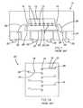
- FIG. 1One such example of a stacked die to lower wire bond loop height is depicted in FIG. 1, shown as an encapsulated package 10 comprising a flip chip mounted on a chip-on-board (“FC-on-chip”).
- the package 10includes a flip chip 12 mounted via solder bumps 14 with the active surface 16 facing down onto the active surface 18 of a bottom die (chip-on-board) 20 , which in turn, is mounted with an adhesive tape or paste 22 onto an interposer substrate 24 .
- Bonding wires 26connect the bond pads 28 on the bottom die 20 to lead or trace ends 30 on the interposer 24 .
- the interposer 24includes solder balls 32 for mounting the encapsulated package (component) 10 onto a substrate, e.g., motherboard, PCB (not shown).
- the bond pads 13 on the flip chip die 12can be wafer bumped, for example, by stencil printing, electrolytic plating or electroless plating, an RDL on the flip chip die 12 may not be necessary, and the die 12 can be directly bonded to the bottom die 20 through an RDL 34 disposed on the surface of the bottom die 20 , as schematically depicted in FIG. 1A, whereby the solder bumps/balls 14 on the flip chip die 12 contact the bond pads 35 of the RDL 34 on the bottom die 20 .
- the pitch of the bond pads 13is tight, it may not be possible to wafer bump the bond pads 13 (e.g., by stencil printing, electrolytic plating, etc), and additional RDL processing on the flip chip die 12 itself may be required.
- the RDL 34functions to provide electrical connection to accommodate the flip chip die 12 in either of these approaches.
- FC-on-chipcan also lead to high costs and process difficulties.
- a flip chip mounteris required to accurately align the top die 12 to the bottom die 20 .
- Another drawbackis that damage can occur to the active surface 18 of the bottom die 20 during an underfilling process onto the active surface 18 , and a molding filler can fail to flow into voids between the dies if the gap is too small.
- the present inventionprovides a flexible film interposer for stacking a tape base flip chip onto a second (bottom) semiconductor die, and semiconductor devices and stacked die assemblies that incorporate the interposer, and methods of fabricating the devices and assemblies for increasing semiconductor device density.
- the present inventionrelates to a stacked multi-substrate device using a combination of flip chip and chip-on-board assemblies to achieve densely packaged semiconductor devices, without the need for a redistribution layer (RDL).
- RDLredistribution layer
- the inventionprovides a flexible film interposer structured for mounting thereon first and second semiconductor die in a stacked die assembly.
- the flexible film interposercomprises a flexible substrate comprising a first surface, a second surface, and opposing sides; a plurality of spaced apart recesses having a base and extending through the flexible substrate for receiving conductive connecting members of a first semiconductor die therein; at least one slot formed through the substrate and disposed between the recesses and a side of the substrate; and a plurality of conductive traces disposed on the second surface of the substrate, each trace extending over the slot and at least one recess, each of the recesses having a trace disposed at the base thereof.
- the flexible film interposercomprises a flexible substrate comprising a first surface, a second surface, and opposing sides.
- the first surface of the substrateis structured for mounting thereon a first semiconductor die having a plurality of spaced apart conductive connecting members disposed on an active surface
- the second surfaceis structured for mounting thereon a second semiconductor die having a plurality of bond pads spaced along a periphery.
- the substratecomprises a plurality of spaced apart recesses having a base and extending through the substrate for receiving the plurality of conductive connecting members of the first semiconductor die therein.
- the substratefurther comprises one or more slots extending therethrough and along a periphery of the substrate, wherein when the second semiconductor die is mounted onto the second surface of the substrate the bonding pads are exposed through the slots.
- the flexible film interposercan further comprise a plurality of conductive traces disposed on the second surface of the substrate, each trace extending over the slot and at least one recess, each of the recesses having a trace disposed at the base thereof.
- the flexible film interposerpreferably comprises a flexible polyimide film (e.g., a flex tape), having a thickness in the range of about 12.5 ⁇ m to about 200 ⁇ m.
- the slotsare sized and configured to receive a bonding tool therethrough to contact bond pads of a semiconductor die mounted on the second surface of the interposer and exposed through the slots.
- An adhesive elementsuch as a double-sided adhesive tape, can be disposed on the first and/or the second surface of the substrate to adhere the semiconductor die thereto.
- the inventionprovides a semiconductor device.
- the semiconductor devicecomprises a flexible film interposer according to the invention and a first semiconductor die mounted thereon, the die having a first active surface and a second surface, and the active surface comprising a plurality of spaced apart conductive connecting members.
- the first semiconductor dieis mounted on the flexible film interposer such that a conductive connecting member of the die is received in a recess of the interposer in conductive contact with the trace at the base of the recess, and the slots on the first surface of the substrate are exposed.
- An underfill encapsulation materialcan be disposed between the active surface of the first semiconductor die and the first surface of the flexible film interposer.
- the semiconductor devicecan further include an adhesive element such as an adhesive paste or tape, disposed between the active surface of the semiconductor die and the flexible film interposer.
- the inventionprovides a stacked die assembly.
- the assemblycomprises a flexible film interposer according to the invention having first and second semiconductor dies mounted on the first and second surfaces, respectively, of a flexible substrate.
- the first semiconductor dieis mounted onto the first surface of the flexible film interposer using a conventional die attacher or a flip chip attacher such that each of a plurality of conductive connecting members of the die is received in each of a plurality of spaced apart recesses of the interposer in conductive contact with a trace at the base of the recess.
- the first (active) surface of the second semiconductor dieis mounted onto the second surface of the flexible film interposer with bond pads on the active surface of the die exposed through the slot(s) of the flexible film interposer.
- An interposer substratecomprising terminal pads on a first surface, is mounted onto the second surface of the second semiconductor die with the terminal pads exposed.
- the traces exposed through the slots of the flexible film interposer and the underlying bond pads of the second semiconductor dieare bonded to the terminal pads of the interposer substrate, for example, by wire bonding or TAB bonding.
- An underfill encapsulation materialcan be disposed between the active surface of the first semiconductor die and the first surface of the flexible film interposer.
- the interposer substratecan comprise a flexible material such as a polyimide substrate, or a non-flexible substrate such as bismaleimide triazine (BT) resin, FR4 fiberglass laminate, FR5 laminate, or ceramic.
- the interposer substratecan also comprise external contacts such as conductive solder balls, to form the stacked die assembly as a component that can be coupled to an external circuitry such as a testing apparatus.
- the interposer substratecan comprise, for example, a PCB substrate, or a motherboard.
- the stacked die assemblycan also be encapsulated to form a package.
- the inventionprovides a semiconductor package.
- the packagecomprises an encapsulated stacked die assembly, which comprises first and second semiconductor dies mounted on a flexible film interposer according to the invention, with the second (bottom) die being mounted on an interposer substrate.
- the inventionprovides a method of fabricating a semiconductor device.
- the methodcomprises the steps of: providing a flexible film interposer, the interposer comprising a first surface and a second surface, at least one elongate slot formed through and along a peripheral edge of the interposer to expose bond pads on a second semiconductor die mounted onto the second surface of the interposer, a plurality of spaced recesses formed through the interposer and adjacent the slot, each recess having a base, and a plurality of conductive traces disposed on the second surface of the interposer, each trace extending across and exposed through the slot and the base of one or more adjacent recesses in a perpendicular orientation to the slot; and mounting a first semiconductor die on the first surface of the flexible film interposer, the first semiconductor die having an active surface comprising a plurality of spaced conductive connecting members, and mounted on the interposer such that a conductive connecting member of the die is received in a recess of
- the inventionprovides a method of fabricating a stacked die assembly.
- the methodcomprises the steps of: providing a flexible film interposer, according to the invention; mounting a first semiconductor die on the first surface of the flexible film interposer, the first semiconductor die having an active surface comprising a plurality of spaced conductive connecting members, and mounted on the interposer such that a conductive connecting member of the die is received in a recess of the interposer in conductive contact with the trace at the base of the recess; mounting a second conductor die on an interposer substrate, the second semiconductor die comprising a first active surface and a second surface, the active surface comprising a bond pad, and the interposer substrate comprising a first surface with terminal pads disposed thereon, and mounted onto the second surface of the second semiconductor die with the terminal pads exposed; mounting the second semiconductor die onto the second surface of the flexible film interposer with the bond pads of the second die exposed through the slot of the interposer; and bonding the traces of
- Either or both of the steps of mounting the first and second semiconductor die on the flexible film interposercan further comprise applying an adhesive element to the surface of the flexible film interposer and/or the surface of the die.
- the step of bondingcan comprise forming contacts in the slots of the flexible film interposer and over the traces and the bond pads of the second semiconductor die, and extending bonding wires from the solder ball contacts to the terminal pads on the interposer substrate.
- the methodcan further comprise the step of encapsulating the stacked die assembly to form a semiconductor package.
- the inventionadvantageously improves the interconnection between a die component and a carrier substrate such as an interposer or PCB, and eliminate the need for a metal re-distribution layer (RDL).
- the inventionalso provides a package with a reduced total assembly height.
- the inventionadditionally eliminates problems associated with prior art underfilling and alignment processes.
- FIG. 1is a cross-sectional, side elevational view of a prior art embodiment of a stacked die package comprising a flip chip mounted on an RDL on a chip-on-board.
- FIG. 1Ais a top plan view of an embodiment of the bottom die of FIG. 1 (with the top die removed), illustrating an RDL.
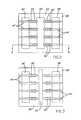
- FIG. 2is a top plan view of an embodiment of a flexible film interposer according to the invention.
- FIG. 3is a bottom plan view of the flexible film interposer of FIG. 2.
- FIG. 3Ais a bottom plan view of an embodiment of the interposer of FIG. 2, having a soldermask layer disposed over the traces.
- FIG. 4is a cross-sectional, side elevational view of the flexible film interposer of FIG. 2, taken along line 4 - 4 .
- FIG. 4Ais a cross-sectional, side elevational view of the interposer depicted in FIG. 3A, taken along line 4 A- 4 A.
- FIGS. 5 - 11illustrates sequential processing steps showing fabrication of a stacked die package according to an embodiment of a method of the invention.
- FIGS. 5 A- 5 Billustrate other embodiments of the step of mounting a flip chip onto an interposer, the embodiment of the flip chip die having a single row of bumps and the interposer having a corresponding row of recesses.
- FIG. 12is a cross-sectional, side elevational view of a second embodiment of a stacked die package fabricated according to the invention.
- the inventionprovides a flexible film interposer for stacking a tape base flip chip onto a second (bottom) die. Recesses are fabricated in the flexible film interposer for the first level interconnect using conventional die mount equipment.
- the flexible film interposerincludes features to interconnect to the second die without the need for an RDL on the second die.
- a flexible film interposer 36 ′according to the invention is depicted in a simplified top plan view.
- the flexible film interposer 36 ′can be formed from known insulating polymeric materials, for example, a flex tape.
- the interposer 36 ′is comprises a flexible polyimide film (e.g., KAPTON from DuPont, Wilmington, Del., or UPILEX from Ube Industries, Ltd., Japan) having a thickness in the range of about 12.5 ⁇ m to about 200 ⁇ m, with thicknesses in the range of about 12.5 ⁇ m to about 50 ⁇ m being preferred.
- a flexible polyimide filme.g., KAPTON from DuPont, Wilmington, Del., or UPILEX from Ube Industries, Ltd., Japan
- the flexible film interposer 36 ′comprises slots or recesses 38 ′ to facilitate a first level interconnection to the bottom die (not shown) by means of TAB or conventional wire bonding.
- the interposer 36 ′also includes multiple recesses or vias 40 ′ for first level interconnection of the top die in a flip chip attachment.
- the recesses 38 ′, 40 ′can be formed through a first (upper) surface 42 ′ of the flexible film interposer 36 ′ by a method known in the art and appropriate to the material employed for the flexible film interposer 36 ′, for example, patterning and utilizing a chemical wet etch or dry etch, mechanical drilling or punching, and laser ablation.
- Each of the recesses 38 ′, 40 ′extend to a bond pad 44 ′ in the form of a conductive trace formed on the second (lower) surface 46 ′ of the interposer 36 ′.
- Such traces 44 ′can be formed by etching a conductive layer disposed on the lower surface 46 ′ of the interposer, or by printing traces onto the lower surface using conductive ink.
- traces 44 ′comprising copper or a copper alloy are utilized.
- the recesses 38 ′are depicted in the form of a slot with the traces 44 ′ extending thereover.
- the recesses (slots) 38 ′are sized and configured to adequately receive therethrough a conventional bonding tool for tape automated bonding (TAB) or wire bonding, typically with a width of about 50 ⁇ m to about 2 mm.
- TABtape automated bonding
- the recesses 38 ′can be formed in any suitable shape, such as square, rectangular, oval, and circular, and may include tapered side walls.
- the multiple recesses (vias) 40 ′are formed in the flexible film interposer 36 ′ in a preselected pattern and having a predetermined size and shape to correspond with a bond pad configuration formed on an active surface of a semiconductor die intended to be attached thereto.
- the recesses 40 ′can be formed with tapered sidewalls (FIG. 4) or straight (vertically oriented) sidewalls (FIG. 5A), as desired.
- the conductive traces (bond pads) 44 ′extend over each of the recesses 40 ′ at the base 48 ′ thereof.
- a soldermask layer 49 ′′can be formed over the traces 44 ′ to provide an overlying insulation layer.
- the soldermaskcomprises a photoimageable dielectric material that can be blanket deposited as a wet or dry film, exposed through a mask, developed and then cured.
- the spaced apart recesses 40 ′are formed in the flexible film interposer 36 ′ in a preselected pattern to correspond with the bond pads and bump configuration of the die (flip chip) to be attached to the interposer 36 ′.
- FIG. 2depicts the multiple recesses 40 ′ in a centrally positioned, four-row configuration in the flexible film interposer 36 ′.
- Such configurationis made to correspond and receive bumps of a bumped semiconductor die (flip chip) having, for example, centrally positioned, four-row bump configuration which will be more fully illustrated and described hereafter.
- Other patterns of the multiple recesses (vias) 40 ′can also be utilized to match with a particular bump configuration. For example, FIGS.
- FIG. 5 A- 5 Billustrate another embodiment of an interposer 36 ′′, 36 ′′′ having a centrally located single row of recesses 40 ′′, 40 ′′′ to correspond with a single row of conductive bumps 60 ′′, 60 ′′′ on the die 54 ′′, 54 ′′′.
- the multiple recesses 40 ′can be formed in any suitable shape including, for example, square, rectangular, oval, and circular, and can include tapered side walls as shown, such that the openings of the recesses 40 ′ are larger than the bases.
- an adhesive element 50 ′, 52 ′can be disposed, respectively, on the first (upper) surface 42 ′ and/or the second (lower) surface 46 ′ of the flexible film interposer 36 ′.
- the adhesive elements 50 ′, 52 ′can be utilized to secure a top (flip chip) die and a bottom die, respectively, to the flexible film interposer 36 ′.
- the adhesive elements 50 ′, 52 ′can comprise any suitable adhesive material known in the art, including contact adhesives, thermoplastic adhesives and thermosetting adhesives, for example, an adhesive gel or paste such as a conventional epoxy or polyimide die bonding adhesive, and/or a double-sided adhesive tape such as polyimide.
- Adhesive element 50 ′can have a thickness such that it functions as a spacer to control the degree of insertion of conductive bumps carried on the top die into recesses 40 ′.
- adhesive element 52 ′can extend onto the traces 44 ′.
- the flexible film interposer 36 ′can be provided in a pre-taped form with an adhesive tape attached thereto, or the adhesive elements 50 ′, 52 ′ can be applied to the flexible film interposer 36 ′ during fabrication of a stacked die assembly or package. In another embodiment (not shown), the adhesive elements 50 ′, 52 ′ can be applied to the active surfaces of the semiconductor die to be attached to the flexible film interposer 36 ′.
- an adhesive tapemay be applied from a dispenser and severed from a roll of tape, or applied from a transfer (carrier) film.
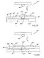
- FIGS. 5 - 11illustrate an embodiment of a method of forming a stacked die package according to the invention utilizing the flexible film interposer 36 ′.
- FIGS. 5 - 7depicts simplified cross-sectional views of the mounting and bonding of the flexible film interposer 36 ′ to a semiconductor die 54 ′ in a flip chip attachment.
- the first (upper) surface 42 ′ of the flexible film interposer 36 ′is aligned with and facing the active surface 56 ′ of the die 54 ′ prior to assembly.
- the active surface 56 ′includes a plurality of bond pads 58 ′ with conductive bumps 60 ′ mounted thereon, which are arranged in a predetermined configuration.
- Recesses 40 ′ in the flexible film interposer 36 ′are sized and configured to correspond to the configuration of the bond pads 58 ′ and the conductive bumps 60 ′.
- the conductive bumps 60 ′typically comprise a metal or alloy such as copper, silver or gold, or a conductive polymer material, and can be formed by known methods in the art, for example, electroplating, metal stud bumping by wire bonders, and stenciling.
- FIG. 6shows the flexible film interposer 36 ′ mounted to the die 54 ′ in a flip chip attachment to form a die/interposer assembly 62 ′, whereby each of the conductive bumps 60 ′ is inserted into a corresponding recess 40 ′ of interposer 36 ′ and engage with the traces (bond pads) 44 ′ at the base 48 ′ of each of the recesses 40 ′.
- the die 54 ′can be attached to the flexible film interposer 36 ′ by the optional adhesive element 50 ′ (e.g., tape, non-conductive die attach paste) disposed on the first (upper) surface of the flexible film interposer 36 ′, or on the active surface 56 ′ of the die 54 ′.
- the optional adhesive element 50 ′e.g., tape, non-conductive die attach paste
- the conductive bumps 60 ′ in the form of solder bumpscan be reflowed to fill the recesses (vias) 40 ′ and physically and electrically bond with the traces (bond pads) 44 ′, or cured in the case of conductive polymer bumps, although other methods such as thermal compression can also be used.
- the conductive bumps 60 ′can also be connected to the traces (bond pads) 44 ′ by means of a conductive paste (not shown) such as a eutectic solder or conductive epoxy, that is applied onto the bumps 60 ′ or into the recesses 40 ′ to provide electrical contact between the bumps 60 ′ and the traces 44 ′, with the bumps 60 ′ then reflowed or cured.
- a dielectric underfill encapsulation material 64 ′as known in the art, such as an epoxy or silicone compound, can be applied between the active die surface 56 ′ and the upper surface 42 ′ of the flexible film interposer 36 ′ to reinforce the connection between the die 54 ′ to the flexible film interposer 36 ′ and protect the bump connections from contamination.
- the underfill material 64 ′is applied by capillary action under pressure, using a dispensing needle 66 ′ as known in the art, whereby the fill material is dispensed around the perimeter of the die 54 ′ and allowed to flow beneath the die to fill the space between the active surface 56 ′ of the die and the upper surface 42 ′ of the interposer 36 ′.
- Other known methods of underfillinginclude gravity and vacuum injecting the underfill material.
- the dielectric materialcan be cured through a chemical reaction, or by the application of UV light or other radiation and/or heat.
- a non-flow underfill materialcan be deposited into the recesses of the flexible film interposer 36 ′ and the flip chip die 54 ′ mounted thereon. For example, as shown in FIG.
- a non-flowable underfill material 64 ′′such as a thermoset or thermoplastic polymer, typically in paste form, can be deposited into the recess 40 ′′ of the interposer 36 ′′, and the flip chip die 54 ′′ can then be die mounted onto the interposer 36 ′′ with the conductive bumps 60 ′′ inserted into underfill 64 ′′ in the recesses 40 ′′, optionally, with the additional use of a tape adhesive 50 ′′ (and/or paste adhesive as desired) applied to the surface 42 ′′ of the interposer.
- a tape adhesive 50 ′′and/or paste adhesive as desired
- a conductive bump 65 ′′can be optionally disposed in the recess 40 ′′ over the traces 44 ′′ to facilitate electrical contact between the bumps 60 ′′ of the flip chip die 54 ′′ with the traces 44 ′′.
- FIG. 5Aalso illustrates an embodiment of a flip chip die 54 ′′ having a single row of conductive bumps 60 ′′ and an interposer 36 ′′ having recesses 40 ′′ in a corresponding single row.
- a non-conductive film and/or paste (e.g., NCF film) 50 ′′′can be applied over the upper surface 42 ′′′ of the interposer 36 ′′′, and the flip chip die 54 ′′′ then die mounted onto the interposer 36 ′′′.
- the film and/or paste 50 ′′′allows the conductive bumps 60 ′′′ of the flip chip die to penetrate therethrough.
- a non-flowable underfill materialcan be deposited in the recesses 40 ′′′ of the interposer 36 ′′′ prior to applying the film and/or paste 50 ′′′.
- conductive bumps 66 ′′′are disposed within the recesses 40 ′′′ for contact between the bumps 60 ′′′ on the flip chip 54 ′′′ and the traces 44 ′′′.
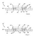
- the flexible film interposer and top die assembly 62 ′is then mounted onto a second (lower) die 68 ′ that has been mounted onto an interposer substrate 70 ′ in a chip-on-board (COB) assembly 72 ′ to form the stacked die assembly 74 ′.
- the second (lower) surface 46 ′ of the flexible film interposer 36 ′is aligned with and facing the active surface 76 ′ of the second (lower) die 68 ′ prior to assembly.
- the interposer/top die assembly 62 ′ and the COB assembly 72 ′can be bonded together using techniques known and used in the art, such as by tape adhesive and/or epoxy adhesive, and the like.
- a conventional assembly processcan be used to prepare the COB assembly 72 ′.
- an active surface 76 ′ of the second die 68 ′includes bond pads 78 ′ along the periphery thereof.
- the interposer substrate 68 ′includes terminal pads 80 ′ on the first (upper) surface 82 ′.
- the die 68 ′has been surface mounted onto the first (upper) surface 82 ′ of the interposer substrate 70 ′ by means of an adhesive element 84 ′, which can comprise any suitable dielectric adhesive known in the art, and be of any suitable form, for example, with a tape adhesive or die attach paste, as described with respect to adhesive elements 50 ′, 52 ′.
- the interposer substrate 70 ′is structured to couple the chip package 98 ′ (FIG. 9) as a component to an electrical apparatus such as a PCB or other external circuitry (not shown) such as a motherboard of a computer, program logic controller (PLC), a testing apparatus, among others.
- Typical interposers 70 ′ for coupling semiconductive devices to an electrical apparatusare comprised of a flexible laminated polymer or polyimide layer, or a non-flexible material such as a bismaleimide triazine (BT) resin, FR4 fiberglass laminate, FR5 laminate, or ceramic.
- BTbismaleimide triazine
- Such interposer substrates 70 ′typically includes a variety of conductive vias (not shown) that extend through the cross-section of the substrate and establish routing of the conductive elements through the substrate 70 ′, and further include electrically conductive metal lines or traces and pads formed on the second (bottom) surface 86 ′ for electrical connection to an external electrical apparatus (not shown).
- External contacts 88 ′in the form of conductive solder balls (or other suitable conductive material such as conductive epoxies or conductor-filled epoxies), columns, pins, and the like, are used to connect the pads on the bottom surface 86 ′ of the interposer substrate 70 ′ to the electrical apparatus.
- the interposer substrate 70 ′can comprise a PCB substrate, motherboard, or other like substrate, whereby the top die/interposer assembly 62 ′ and bottom die 68 ′ are mounted directly thereon, and external contacts 88 ′ are omitted.
- This structurefunctions as a board level device such as a module or a motherboard.
- the traces (bond pads) 44 ′ in the recesses 38 ′are aligned with corresponding bond pads 76 ′ of the bottom die 68 ′.
- Conventional assembly devicessuch as aligner bonder tools (e.g., LOC mounter) can be used to align and then bond the bottom die 68 ′ to the flexible film interposer 36 ′.
- a split optics systemcan also be used to view aligned portions of the die and the substrate.
- FIGS. 9 - 10depict the assemblies 62 ′, 72 ′ mounted to form a stacked die assembly 74 ′.
- Wire bonding or TAB bondingis performed to join the traces (bond pads) 44 ′ to the bond pads 78 ′ of the bottom die 68 ′, and to the terminal pads 80 ′ on the interposer substrate 70 ′.
- the recesses 38 ′are sized to permit access for a bonding tool such as a wire bond capillary (not shown), to the bond pads 78 ′ of the bottom die 68 ′.
- the bonding toolcan be configured, for example, for thermosonically bonding, thermocompression bonding, tape-automated bonding (TAB), or other method known in the art.
- thermosonic bonding with a ball bond 90 ′is used.
- Ball bonds 90 ′are formed in the recesses 38 ′ over the traces (bond pads) 44 ′ and the bond pads 78 ′ of the bottom die 68 ′, thus joining the bond pads 44 ′, 76 ′ together in one operation, as best seen in FIG. 11.
- the bond wires 92 ′are extended and bonded to the terminal pads 80 ′ on the interposer substrate 70 ′.
- the ball bonds 90 ′function to bond together the flexible film interposer 38 ′, the bottom die 68 ′ and the interposer substrate 70 ′.
- TAB bonding and ultrasonic bondingcan be used to connect the traces 44 ′′ and the bond pads 78 ′′.
- the wire-bonded stacked die assembly 82 ′can be partially or fully encapsulated with a dielectric encapsulation material 96 ′ using known techniques in the art to form an encapsulated stacked die package 98 ′, for example, by spin-coating, glob-top, pot molding, and transfer molding.
- the methodcan be utilized to fabricate an assembly comprising additional stacked die layers, such as the embodiment depicted in FIG. 12.
- a semiconductor die 100 ′′has been surface mounted by means of an adhesive element 102 ′′ onto the second (inactive) surface 104 ′′ of the die (flip chip) 54 ′′.
- Additional die 116 ′′ mounted on a flexible film interposer 118 ′′ having recesses 38 ′′ (assembly 122 ′′)can be mounted on the die 100 ′′ and bonded to the interposer 70 ′′ as described hereinabove. Bond pads 106 ′′ can then be bonded as described previously to terminal pads 112 ′′ on the interposer substrate 70 ′′.
- Further diescan be added to the stacked die assembly by alternating a surface mounted die ( 100 ′′) and a flip chip/flexible film interposer assembly ( 120 ′′).
- the flexible film interposer of the inventionfunctions to redistribute and connect the bond pads of the bottom die to bond pads of the upper (flip chip) die, advantageously replacing the RDL ( 34 ) required in a conventional flip chip attachment, as in FIG. 1, and at less cost than a conventional RDL.
- the design of the flexible film interposer including the relatively large size of the recesses (vias)provides improved accuracy with mounting the upper (flip chip) die to the bottom die, being readily achievable using a conventional die mounting device.
- the recesses (slots)are sized to readily receive a bonding tool therethrough to bond the traces and bond pads on the bottom die to an interposer carrier substrate in one operation.
- the present packageachieves a desirably low package profile.
- the package designalso utilizes conventional underfill processes that are carried out on the surface of the flexible interposer substrate rather than the active surface of the bottom die, thus reducing yield and process difficulties.
Landscapes
- Engineering & Computer Science (AREA)
- Microelectronics & Electronic Packaging (AREA)
- Power Engineering (AREA)
- Physics & Mathematics (AREA)
- Condensed Matter Physics & Semiconductors (AREA)
- General Physics & Mathematics (AREA)
- Computer Hardware Design (AREA)
- Manufacturing & Machinery (AREA)
- Wire Bonding (AREA)
Abstract
Description
- This invention generally relates to assembling and packaging multiple semiconductor dies, and more particularly to a stacked multiple die device and methods for fabricating the device.[0001]
- Chip-on-board and board-on-chip (BOC) techniques are used to attach semiconductor dies to an interposer or other carrier substrate such as a printed circuit board (PCB). Attachment can be achieved through flip chip attachment, wirebonding, or tape automated bonding (“TAB”).[0002]
- Flip chip attachment typically utilizes ball grid array (BGA) technology. The BGA component (die) includes conductive external contacts, typically in the form of solder balls or bumps, arranged in a grid pattern on the active surface of the die, which permit the die to be flip chip mounted to an interposer or other carrier substrate (e.g., PCB).[0003]
- In a flip chip attachment, the balls of the BGA component are aligned with terminals on the carrier substrate, and connected by reflowing the solder balls. The solder balls can be replaced with a conductive polymer that is cured. A dielectric underfill is then interjected between the flip chip die and the surface of the carrier substance to embed the solder balls and mechanically couple the BGA component to the carrier substrate.[0004]
- Wirebonding and TAB attachment generally involve attaching a die by its backside to the surface of a carrier substrate with an appropriate adhesive (e.g., epoxy) or tape. With wirebonding, bond wires are attached to each bond pad on the die and bonded to a corresponding terminal pad on the carrier substrate (e.g., interposer). With TAB, ends of metal leads carried on a flexible insulating tape such as a polyimide, are attached to the bond pads on the die and to the terminal pads on the carrier substrate. A dielectric (e.g., silicon or epoxy) is generally used to cover the bond wires or metal tape leads to prevent damage.[0005]
- High performance, low cost, increased miniaturization of components, and greater packaging density of integrated circuits have long been goals of the computer industry. One method of increasing integrated circuit density while reducing package size and height is to stack dies vertically. Different approaches to packaging have been pursued to provide stacked die devices.[0006]
- One such example of a stacked die to lower wire bond loop height is depicted in FIG. 1, shown as an[0007]
encapsulated package 10 comprising a flip chip mounted on a chip-on-board (“FC-on-chip”). As shown, thepackage 10 includes aflip chip 12 mounted viasolder bumps 14 with theactive surface 16 facing down onto theactive surface 18 of a bottom die (chip-on-board)20, which in turn, is mounted with an adhesive tape or paste22 onto aninterposer substrate 24.Bonding wires 26 connect thebond pads 28 on thebottom die 20 to lead ortrace ends 30 on theinterposer 24. Theinterposer 24 includessolder balls 32 for mounting the encapsulated package (component)10 onto a substrate, e.g., motherboard, PCB (not shown). - Flip chip attachment has provided improved electrical performance and allowed greater packaging density. However, developments in ball grid array technology has produced arrays in which the balls are made smaller and with tighter pitches. As the balls become smaller and are set closer together, it poses problems for the mutual alignment of the[0008]
conductive bumps 14 on theflip chip die 12 with thebond pads 28 on thebottom die 20, requiring a metal reroute or redistribution layer (RDL)34 disposed as an intermediate layer on the surface of thebottom die 20. TheRDL 34 effects an electrical interconnection (redistribution) between thebond pads 13 on theflip chip die 12 to thebond pads 28 on thebottom die 20 for die attachment and wire bonding to the substrate. If thebond pads 13 on theflip chip die 12 can be wafer bumped, for example, by stencil printing, electrolytic plating or electroless plating, an RDL on theflip chip die 12 may not be necessary, and the die12 can be directly bonded to thebottom die 20 through anRDL 34 disposed on the surface of thebottom die 20, as schematically depicted in FIG. 1A, whereby the solder bumps/balls 14 on the flip chip die12 contact thebond pads 35 of the RDL34 on the bottom die20. However, if the pitch of thebond pads 13 is tight, it may not be possible to wafer bump the bond pads13 (e.g., by stencil printing, electrolytic plating, etc), and additional RDL processing on theflip chip die 12 itself may be required. TheRDL 34 functions to provide electrical connection to accommodate theflip chip die 12 in either of these approaches. - Fabricating an FC-on-chip can also lead to high costs and process difficulties. For Example, a flip chip mounter is required to accurately align the[0009]
top die 12 to the bottom die20. Another drawback is that damage can occur to theactive surface 18 of thebottom die 20 during an underfilling process onto theactive surface 18, and a molding filler can fail to flow into voids between the dies if the gap is too small. - In view of these and other deficiencies in conventional methods for fabricating stacked die modules, improvements in fabrication methods are desirable.[0010]
- The present invention provides a flexible film interposer for stacking a tape base flip chip onto a second (bottom) semiconductor die, and semiconductor devices and stacked die assemblies that incorporate the interposer, and methods of fabricating the devices and assemblies for increasing semiconductor device density. In particular, the present invention relates to a stacked multi-substrate device using a combination of flip chip and chip-on-board assemblies to achieve densely packaged semiconductor devices, without the need for a redistribution layer (RDL).[0011]
- In one aspect, the invention provides a flexible film interposer structured for mounting thereon first and second semiconductor die in a stacked die assembly. In one embodiment, the flexible film interposer comprises a flexible substrate comprising a first surface, a second surface, and opposing sides; a plurality of spaced apart recesses having a base and extending through the flexible substrate for receiving conductive connecting members of a first semiconductor die therein; at least one slot formed through the substrate and disposed between the recesses and a side of the substrate; and a plurality of conductive traces disposed on the second surface of the substrate, each trace extending over the slot and at least one recess, each of the recesses having a trace disposed at the base thereof.[0012]
- In another embodiment, the flexible film interposer comprises a flexible substrate comprising a first surface, a second surface, and opposing sides. The first surface of the substrate is structured for mounting thereon a first semiconductor die having a plurality of spaced apart conductive connecting members disposed on an active surface, and the second surface is structured for mounting thereon a second semiconductor die having a plurality of bond pads spaced along a periphery. The substrate comprises a plurality of spaced apart recesses having a base and extending through the substrate for receiving the plurality of conductive connecting members of the first semiconductor die therein. The substrate further comprises one or more slots extending therethrough and along a periphery of the substrate, wherein when the second semiconductor die is mounted onto the second surface of the substrate the bonding pads are exposed through the slots. The flexible film interposer can further comprise a plurality of conductive traces disposed on the second surface of the substrate, each trace extending over the slot and at least one recess, each of the recesses having a trace disposed at the base thereof.[0013]
- The flexible film interposer preferably comprises a flexible polyimide film (e.g., a flex tape), having a thickness in the range of about 12.5 μm to about 200 μm. The slots are sized and configured to receive a bonding tool therethrough to contact bond pads of a semiconductor die mounted on the second surface of the interposer and exposed through the slots. An adhesive element such as a double-sided adhesive tape, can be disposed on the first and/or the second surface of the substrate to adhere the semiconductor die thereto.[0014]
- In another aspect, the invention provides a semiconductor device. In one embodiment, the semiconductor device comprises a flexible film interposer according to the invention and a first semiconductor die mounted thereon, the die having a first active surface and a second surface, and the active surface comprising a plurality of spaced apart conductive connecting members. The first semiconductor die is mounted on the flexible film interposer such that a conductive connecting member of the die is received in a recess of the interposer in conductive contact with the trace at the base of the recess, and the slots on the first surface of the substrate are exposed. An underfill encapsulation material can be disposed between the active surface of the first semiconductor die and the first surface of the flexible film interposer. The semiconductor device can further include an adhesive element such as an adhesive paste or tape, disposed between the active surface of the semiconductor die and the flexible film interposer.[0015]
- In another aspect, the invention provides a stacked die assembly. In one embodiment, the assembly comprises a flexible film interposer according to the invention having first and second semiconductor dies mounted on the first and second surfaces, respectively, of a flexible substrate. The first semiconductor die is mounted onto the first surface of the flexible film interposer using a conventional die attacher or a flip chip attacher such that each of a plurality of conductive connecting members of the die is received in each of a plurality of spaced apart recesses of the interposer in conductive contact with a trace at the base of the recess. The first (active) surface of the second semiconductor die is mounted onto the second surface of the flexible film interposer with bond pads on the active surface of the die exposed through the slot(s) of the flexible film interposer. An interposer substrate comprising terminal pads on a first surface, is mounted onto the second surface of the second semiconductor die with the terminal pads exposed. The traces exposed through the slots of the flexible film interposer and the underlying bond pads of the second semiconductor die are bonded to the terminal pads of the interposer substrate, for example, by wire bonding or TAB bonding. An underfill encapsulation material can be disposed between the active surface of the first semiconductor die and the first surface of the flexible film interposer. The interposer substrate can comprise a flexible material such as a polyimide substrate, or a non-flexible substrate such as bismaleimide triazine (BT) resin, FR4 fiberglass laminate, FR5 laminate, or ceramic. The interposer substrate can also comprise external contacts such as conductive solder balls, to form the stacked die assembly as a component that can be coupled to an external circuitry such as a testing apparatus. In another embodiment, the interposer substrate can comprise, for example, a PCB substrate, or a motherboard. The stacked die assembly can also be encapsulated to form a package.[0016]
- In yet another aspect, the invention provides a semiconductor package. In one embodiment, the package comprises an encapsulated stacked die assembly, which comprises first and second semiconductor dies mounted on a flexible film interposer according to the invention, with the second (bottom) die being mounted on an interposer substrate.[0017]
- In a further aspect, the invention provides a method of fabricating a semiconductor device. In one embodiment, the method comprises the steps of: providing a flexible film interposer, the interposer comprising a first surface and a second surface, at least one elongate slot formed through and along a peripheral edge of the interposer to expose bond pads on a second semiconductor die mounted onto the second surface of the interposer, a plurality of spaced recesses formed through the interposer and adjacent the slot, each recess having a base, and a plurality of conductive traces disposed on the second surface of the interposer, each trace extending across and exposed through the slot and the base of one or more adjacent recesses in a perpendicular orientation to the slot; and mounting a first semiconductor die on the first surface of the flexible film interposer, the first semiconductor die having an active surface comprising a plurality of spaced conductive connecting members, and mounted on the interposer such that a conductive connecting member of the die is received in a recess of the interposer in conductive contact with the trace at the base of the recess.[0018]
- In another aspect, the invention provides a method of fabricating a stacked die assembly. In one embodiment, the method comprises the steps of: providing a flexible film interposer, according to the invention; mounting a first semiconductor die on the first surface of the flexible film interposer, the first semiconductor die having an active surface comprising a plurality of spaced conductive connecting members, and mounted on the interposer such that a conductive connecting member of the die is received in a recess of the interposer in conductive contact with the trace at the base of the recess; mounting a second conductor die on an interposer substrate, the second semiconductor die comprising a first active surface and a second surface, the active surface comprising a bond pad, and the interposer substrate comprising a first surface with terminal pads disposed thereon, and mounted onto the second surface of the second semiconductor die with the terminal pads exposed; mounting the second semiconductor die onto the second surface of the flexible film interposer with the bond pads of the second die exposed through the slot of the interposer; and bonding the traces of the flexible film interposer and the bond pads of the second semiconductor die to the terminal pads of the interposer substrate. Either or both of the steps of mounting the first and second semiconductor die on the flexible film interposer can further comprise applying an adhesive element to the surface of the flexible film interposer and/or the surface of the die. The step of bonding can comprise forming contacts in the slots of the flexible film interposer and over the traces and the bond pads of the second semiconductor die, and extending bonding wires from the solder ball contacts to the terminal pads on the interposer substrate. The method can further comprise the step of encapsulating the stacked die assembly to form a semiconductor package.[0019]
- The invention advantageously improves the interconnection between a die component and a carrier substrate such as an interposer or PCB, and eliminate the need for a metal re-distribution layer (RDL). The invention also provides a package with a reduced total assembly height. The invention additionally eliminates problems associated with prior art underfilling and alignment processes.[0020]
- Preferred embodiments of the invention are described below with reference to the following accompanying drawings, which are for illustrative purposes only. Throughout the following views, the reference numerals will be used in the drawings, and the same reference numerals will be used throughout the several views and in the description to indicate same or like parts.[0021]
- FIG. 1 is a cross-sectional, side elevational view of a prior art embodiment of a stacked die package comprising a flip chip mounted on an RDL on a chip-on-board. FIG. 1A is a top plan view of an embodiment of the bottom die of FIG. 1 (with the top die removed), illustrating an RDL.[0022]
- FIG. 2 is a top plan view of an embodiment of a flexible film interposer according to the invention.[0023]
- FIG. 3 is a bottom plan view of the flexible film interposer of FIG. 2. FIG. 3A is a bottom plan view of an embodiment of the interposer of FIG. 2, having a soldermask layer disposed over the traces.[0024]
- FIG. 4 is a cross-sectional, side elevational view of the flexible film interposer of FIG. 2, taken along line[0025]4-4. FIG. 4A is a cross-sectional, side elevational view of the interposer depicted in FIG. 3A, taken along
line 4A-4A. - FIGS.[0026]5-11 illustrates sequential processing steps showing fabrication of a stacked die package according to an embodiment of a method of the invention. FIGS.5A-5B illustrate other embodiments of the step of mounting a flip chip onto an interposer, the embodiment of the flip chip die having a single row of bumps and the interposer having a corresponding row of recesses.
- FIG. 12 is a cross-sectional, side elevational view of a second embodiment of a stacked die package fabricated according to the invention.[0027]
- The invention will be described generally with reference to the drawings for the purpose of illustrating embodiments only and not for purposes of limiting the same. The figures illustrate processing steps for use in fabricating semiconductor devices in accordance with the present invention. It should be readily apparent that the processing steps are only a portion of the entire fabrication process.[0028]
- The invention provides a flexible film interposer for stacking a tape base flip chip onto a second (bottom) die. Recesses are fabricated in the flexible film interposer for the first level interconnect using conventional die mount equipment. The flexible film interposer includes features to interconnect to the second die without the need for an RDL on the second die.[0029]
- Referring to FIGS.[0030]2-4, an embodiment of a
flexible film interposer 36′ according to the invention is depicted in a simplified top plan view. Theflexible film interposer 36′ can be formed from known insulating polymeric materials, for example, a flex tape. In preferred implementations, theinterposer 36′ is comprises a flexible polyimide film (e.g., KAPTON from DuPont, Wilmington, Del., or UPILEX from Ube Industries, Ltd., Japan) having a thickness in the range of about 12.5 μm to about 200 μm, with thicknesses in the range of about 12.5 μm to about 50 μm being preferred. - According to the invention, the[0031]
flexible film interposer 36′ comprises slots or recesses38′ to facilitate a first level interconnection to the bottom die (not shown) by means of TAB or conventional wire bonding. Theinterposer 36′ also includes multiple recesses orvias 40′ for first level interconnection of the top die in a flip chip attachment. - The[0032]
recesses 38′,40′ can be formed through a first (upper) surface42′ of theflexible film interposer 36′ by a method known in the art and appropriate to the material employed for theflexible film interposer 36′, for example, patterning and utilizing a chemical wet etch or dry etch, mechanical drilling or punching, and laser ablation. Each of therecesses 38′,40′ extend to abond pad 44′ in the form of a conductive trace formed on the second (lower)surface 46′ of theinterposer 36′.Such traces 44′ can be formed by etching a conductive layer disposed on thelower surface 46′ of the interposer, or by printing traces onto the lower surface using conductive ink. Preferably, traces44′ comprising copper or a copper alloy are utilized. - As shown in a bottom plan view in FIG. 3, the[0033]
recesses 38′ are depicted in the form of a slot with thetraces 44′ extending thereover. The recesses (slots)38′ are sized and configured to adequately receive therethrough a conventional bonding tool for tape automated bonding (TAB) or wire bonding, typically with a width of about 50 μm to about 2 mm. Therecesses 38′ can be formed in any suitable shape, such as square, rectangular, oval, and circular, and may include tapered side walls. - The multiple recesses (vias)[0034]40′ are formed in the
flexible film interposer 36′ in a preselected pattern and having a predetermined size and shape to correspond with a bond pad configuration formed on an active surface of a semiconductor die intended to be attached thereto. Therecesses 40′ can be formed with tapered sidewalls (FIG. 4) or straight (vertically oriented) sidewalls (FIG. 5A), as desired. The conductive traces (bond pads)44′ extend over each of therecesses 40′ at the base48′ thereof. Optionally, as shown in FIGS.3A-4A, asoldermask layer 49″ can be formed over thetraces 44′ to provide an overlying insulation layer. Typically, the soldermask comprises a photoimageable dielectric material that can be blanket deposited as a wet or dry film, exposed through a mask, developed and then cured. - The spaced apart recesses[0035]40′ are formed in the
flexible film interposer 36′ in a preselected pattern to correspond with the bond pads and bump configuration of the die (flip chip) to be attached to theinterposer 36′. For example, FIG. 2 depicts themultiple recesses 40′ in a centrally positioned, four-row configuration in theflexible film interposer 36′. Such configuration is made to correspond and receive bumps of a bumped semiconductor die (flip chip) having, for example, centrally positioned, four-row bump configuration which will be more fully illustrated and described hereafter. Other patterns of the multiple recesses (vias)40′ can also be utilized to match with a particular bump configuration. For example, FIGS.5A-5B illustrate another embodiment of aninterposer 36″,36′″ having a centrally located single row ofrecesses 40″,40′″ to correspond with a single row ofconductive bumps 60″,60′″ on the die54″,54′″. In addition, themultiple recesses 40′ can be formed in any suitable shape including, for example, square, rectangular, oval, and circular, and can include tapered side walls as shown, such that the openings of therecesses 40′ are larger than the bases. - Optionally, an[0036]
adhesive element 50′,52′ can be disposed, respectively, on the first (upper) surface42′ and/or the second (lower)surface 46′ of theflexible film interposer 36′. Theadhesive elements 50′,52′ can be utilized to secure a top (flip chip) die and a bottom die, respectively, to theflexible film interposer 36′. Theadhesive elements 50′,52′ can comprise any suitable adhesive material known in the art, including contact adhesives, thermoplastic adhesives and thermosetting adhesives, for example, an adhesive gel or paste such as a conventional epoxy or polyimide die bonding adhesive, and/or a double-sided adhesive tape such as polyimide.Adhesive element 50′ can have a thickness such that it functions as a spacer to control the degree of insertion of conductive bumps carried on the top die intorecesses 40′. Although not shown,adhesive element 52′ can extend onto thetraces 44′. Theflexible film interposer 36′ can be provided in a pre-taped form with an adhesive tape attached thereto, or theadhesive elements 50′,52′ can be applied to theflexible film interposer 36′ during fabrication of a stacked die assembly or package. In another embodiment (not shown), theadhesive elements 50′,52′ can be applied to the active surfaces of the semiconductor die to be attached to theflexible film interposer 36′. Many suitable adhesive application methods for liquid or gel adhesive application are known in the art, such as screen printing, roller applicator, spray, and transfer. Similarly, an adhesive tape may be applied from a dispenser and severed from a roll of tape, or applied from a transfer (carrier) film. - FIGS.[0037]5-11 illustrate an embodiment of a method of forming a stacked die package according to the invention utilizing the
flexible film interposer 36′. - FIGS.[0038]5-7 depicts simplified cross-sectional views of the mounting and bonding of the
flexible film interposer 36′ to a semiconductor die54′ in a flip chip attachment. As shown in FIG. 5, the first (upper) surface42′ of theflexible film interposer 36′ is aligned with and facing theactive surface 56′ of the die54′ prior to assembly. Theactive surface 56′ includes a plurality ofbond pads 58′ withconductive bumps 60′ mounted thereon, which are arranged in a predetermined configuration.Recesses 40′ in theflexible film interposer 36′ are sized and configured to correspond to the configuration of thebond pads 58′ and theconductive bumps 60′. Theconductive bumps 60′ typically comprise a metal or alloy such as copper, silver or gold, or a conductive polymer material, and can be formed by known methods in the art, for example, electroplating, metal stud bumping by wire bonders, and stenciling. - FIG. 6 shows the[0039]
flexible film interposer 36′ mounted to the die54′ in a flip chip attachment to form a die/interposer assembly 62′, whereby each of theconductive bumps 60′ is inserted into acorresponding recess 40′ ofinterposer 36′ and engage with the traces (bond pads)44′ at the base48′ of each of therecesses 40′. The die54′ can be attached to theflexible film interposer 36′ by the optionaladhesive element 50′ (e.g., tape, non-conductive die attach paste) disposed on the first (upper) surface of theflexible film interposer 36′, or on theactive surface 56′ of the die54′. Theconductive bumps 60′ in the form of solder bumps can be reflowed to fill the recesses (vias)40′ and physically and electrically bond with the traces (bond pads)44′, or cured in the case of conductive polymer bumps, although other methods such as thermal compression can also be used. Theconductive bumps 60′ can also be connected to the traces (bond pads)44′ by means of a conductive paste (not shown) such as a eutectic solder or conductive epoxy, that is applied onto thebumps 60′ or into therecesses 40′ to provide electrical contact between thebumps 60′ and thetraces 44′, with thebumps 60′ then reflowed or cured. - As depicted in FIGS.[0040]6-7, a dielectric
underfill encapsulation material 64′ as known in the art, such as an epoxy or silicone compound, can be applied between theactive die surface 56′ and theupper surface 42′ of theflexible film interposer 36′ to reinforce the connection between the die54′ to theflexible film interposer 36′ and protect the bump connections from contamination. Preferably, theunderfill material 64′ is applied by capillary action under pressure, using a dispensingneedle 66′ as known in the art, whereby the fill material is dispensed around the perimeter of the die54′ and allowed to flow beneath the die to fill the space between theactive surface 56′ of the die and theupper surface 42′ of theinterposer 36′. Other known methods of underfilling include gravity and vacuum injecting the underfill material. The dielectric material can be cured through a chemical reaction, or by the application of UV light or other radiation and/or heat. - Instead of utilizing the above-described underfill process (FIGS.[0041]6-7), a non-flow underfill material can be deposited into the recesses of the
flexible film interposer 36′ and the flip chip die54′ mounted thereon. For example, as shown in FIG. 5A, anon-flowable underfill material 64″ such as a thermoset or thermoplastic polymer, typically in paste form, can be deposited into therecess 40″ of theinterposer 36″, and the flip chip die54″ can then be die mounted onto theinterposer 36″ with theconductive bumps 60″ inserted intounderfill 64″ in therecesses 40″, optionally, with the additional use of a tape adhesive50″ (and/or paste adhesive as desired) applied to thesurface 42″ of the interposer. In the embodiment of theinterposer 36″ shown in FIG. 5A, aconductive bump 65″ can be optionally disposed in therecess 40″ over thetraces 44″ to facilitate electrical contact between thebumps 60″ of the flip chip die54″ with thetraces 44″. FIG. 5A also illustrates an embodiment of a flip chip die54″ having a single row ofconductive bumps 60″ and aninterposer 36″ havingrecesses 40″ in a corresponding single row. - In another embodiment, as shown in FIG. 5B, a non-conductive film and/or paste (e.g., NCF film)[0042]50′″ can be applied over the
upper surface 42′″ of theinterposer 36′″, and the flip chip die54′″ then die mounted onto theinterposer 36′″. The film and/orpaste 50′″ allows theconductive bumps 60′″ of the flip chip die to penetrate therethrough. Optionally, a non-flowable underfill material can be deposited in therecesses 40′″ of theinterposer 36′″ prior to applying the film and/orpaste 50′″. Similar to FIG. 5A,conductive bumps 66′″ are disposed within therecesses 40′″ for contact between thebumps 60′″ on theflip chip 54′″ and thetraces 44′″. - The flexible film interposer and[0043]
top die assembly 62′ is then mounted onto a second (lower) die68′ that has been mounted onto aninterposer substrate 70′ in a chip-on-board (COB)assembly 72′ to form the stackeddie assembly 74′. As shown in FIG. 8, the second (lower)surface 46′ of theflexible film interposer 36′ is aligned with and facing theactive surface 76′ of the second (lower) die68′ prior to assembly. The interposer/top die assembly 62′ and theCOB assembly 72′ can be bonded together using techniques known and used in the art, such as by tape adhesive and/or epoxy adhesive, and the like. - A conventional assembly process can used to prepare the[0044]
COB assembly 72′. As shown, anactive surface 76′ of thesecond die 68′ includesbond pads 78′ along the periphery thereof. Theinterposer substrate 68′ includesterminal pads 80′ on the first (upper) surface82′. The die68′ has been surface mounted onto the first (upper) surface82′ of theinterposer substrate 70′ by means of anadhesive element 84′, which can comprise any suitable dielectric adhesive known in the art, and be of any suitable form, for example, with a tape adhesive or die attach paste, as described with respect toadhesive elements 50′,52′. - In the illustrated embodiment in FIG. 9, the[0045]
interposer substrate 70′ is structured to couple thechip package 98′ (FIG. 9) as a component to an electrical apparatus such as a PCB or other external circuitry (not shown) such as a motherboard of a computer, program logic controller (PLC), a testing apparatus, among others.Typical interposers 70′ for coupling semiconductive devices to an electrical apparatus are comprised of a flexible laminated polymer or polyimide layer, or a non-flexible material such as a bismaleimide triazine (BT) resin, FR4 fiberglass laminate, FR5 laminate, or ceramic.Such interposer substrates 70′ typically includes a variety of conductive vias (not shown) that extend through the cross-section of the substrate and establish routing of the conductive elements through thesubstrate 70′, and further include electrically conductive metal lines or traces and pads formed on the second (bottom) surface86′ for electrical connection to an external electrical apparatus (not shown).External contacts 88′ in the form of conductive solder balls (or other suitable conductive material such as conductive epoxies or conductor-filled epoxies), columns, pins, and the like, are used to connect the pads on thebottom surface 86′ of theinterposer substrate 70′ to the electrical apparatus. - In another embodiment, the[0046]
interposer substrate 70′ can comprise a PCB substrate, motherboard, or other like substrate, whereby the top die/interposer assembly 62′ and bottom die68′ are mounted directly thereon, andexternal contacts 88′ are omitted. This structure functions as a board level device such as a module or a motherboard. - Referring to FIG. 8, in mounting the[0047]
assemblies 62′,72′, the traces (bond pads)44′ in therecesses 38′ are aligned withcorresponding bond pads 76′ of the bottom die68′. Conventional assembly devices such as aligner bonder tools (e.g., LOC mounter) can be used to align and then bond the bottom die68′ to theflexible film interposer 36′. A split optics system can also be used to view aligned portions of the die and the substrate. - FIGS.[0048]9-10 depict the
assemblies 62′,72′ mounted to form astacked die assembly 74′. Wire bonding or TAB bonding is performed to join the traces (bond pads)44′ to thebond pads 78′ of the bottom die68′, and to theterminal pads 80′ on theinterposer substrate 70′. Therecesses 38′ are sized to permit access for a bonding tool such as a wire bond capillary (not shown), to thebond pads 78′ of the bottom die68′. The bonding tool can be configured, for example, for thermosonically bonding, thermocompression bonding, tape-automated bonding (TAB), or other method known in the art. - In the illustrated example in FIG. 9, thermosonic bonding with a[0049]
ball bond 90′ is used.Ball bonds 90′ are formed in therecesses 38′ over the traces (bond pads)44′ and thebond pads 78′ of the bottom die68′, thus joining thebond pads 44′,76′ together in one operation, as best seen in FIG. 11. Thebond wires 92′ are extended and bonded to theterminal pads 80′ on theinterposer substrate 70′. The ball bonds90′ function to bond together theflexible film interposer 38′, the bottom die68′ and theinterposer substrate 70′. In other embodiments, TAB bonding and ultrasonic bonding, as known and used in the art, can be used to connect thetraces 44″ and thebond pads 78″. - Referring again to FIG. 9, the wire-bonded[0050]
stacked die assembly 82′ can be partially or fully encapsulated with adielectric encapsulation material 96′ using known techniques in the art to form an encapsulatedstacked die package 98′, for example, by spin-coating, glob-top, pot molding, and transfer molding. - The method can be utilized to fabricate an assembly comprising additional stacked die layers, such as the embodiment depicted in FIG. 12. As shown, a[0051]
semiconductor die 100″ has been surface mounted by means of anadhesive element 102″ onto the second (inactive)surface 104″ of the die (flip chip)54″.Additional die 116″ mounted on aflexible film interposer 118″ havingrecesses 38″ (assembly122″) can be mounted on thedie 100″ and bonded to theinterposer 70″ as described hereinabove.Bond pads 106″ can then be bonded as described previously toterminal pads 112″ on theinterposer substrate 70″. Further dies can be added to the stacked die assembly by alternating a surface mounted die (100″) and a flip chip/flexible film interposer assembly (120″). - The flexible film interposer of the invention functions to redistribute and connect the bond pads of the bottom die to bond pads of the upper (flip chip) die, advantageously replacing the RDL ([0052]34) required in a conventional flip chip attachment, as in FIG. 1, and at less cost than a conventional RDL. In addition, the design of the flexible film interposer including the relatively large size of the recesses (vias) provides improved accuracy with mounting the upper (flip chip) die to the bottom die, being readily achievable using a conventional die mounting device. Further, the recesses (slots) are sized to readily receive a bonding tool therethrough to bond the traces and bond pads on the bottom die to an interposer carrier substrate in one operation.
- In addition, the present package achieves a desirably low package profile. The package design also utilizes conventional underfill processes that are carried out on the surface of the flexible interposer substrate rather than the active surface of the bottom die, thus reducing yield and process difficulties.[0053]
- In compliance with the statute, the invention has been described in language more or less specific as to structural and methodical features. It is to be understood, however, that the invention is not limited to the specific features shown and described, since the means herein disclosed comprise preferred forms of putting the invention into effect. The invention is, therefore, claimed in any of its forms or modifications within the proper scope of the appended claims appropriately interpreted in accordance with the doctrine of equivalents.[0054]
Claims (115)
Priority Applications (3)
| Application Number | Priority Date | Filing Date | Title |
|---|---|---|---|
| US10/853,377US7189593B2 (en) | 2002-01-09 | 2004-05-25 | Elimination of RDL using tape base flip chip on flex for die stacking |
| US11/714,072US8125065B2 (en) | 2002-01-09 | 2007-03-05 | Elimination of RDL using tape base flip chip on flex for die stacking |
| US13/407,003US8441113B2 (en) | 2002-01-09 | 2012-02-28 | Elimination of RDL using tape base flip chip on flex for die stacking |
Applications Claiming Priority (2)
| Application Number | Priority Date | Filing Date | Title |
|---|---|---|---|
| SG200200130ASG104293A1 (en) | 2002-01-09 | 2002-01-09 | Elimination of rdl using tape base flip chip on flex for die stacking |
| SG200200130 | 2002-01-09 |
Related Child Applications (2)
| Application Number | Title | Priority Date | Filing Date |
|---|---|---|---|
| US10/853,377DivisionUS7189593B2 (en) | 2002-01-09 | 2004-05-25 | Elimination of RDL using tape base flip chip on flex for die stacking |
| US11/714,072DivisionUS8125065B2 (en) | 2002-01-09 | 2007-03-05 | Elimination of RDL using tape base flip chip on flex for die stacking |
Publications (2)
| Publication Number | Publication Date |
|---|---|
| US20030134450A1true US20030134450A1 (en) | 2003-07-17 |
| US7129584B2 US7129584B2 (en) | 2006-10-31 |
Family
ID=32847161
Family Applications (4)
| Application Number | Title | Priority Date | Filing Date |
|---|---|---|---|
| US10/050,507Expired - LifetimeUS7129584B2 (en) | 2002-01-09 | 2002-01-16 | Elimination of RDL using tape base flip chip on flex for die stacking |
| US10/853,377Expired - LifetimeUS7189593B2 (en) | 2002-01-09 | 2004-05-25 | Elimination of RDL using tape base flip chip on flex for die stacking |
| US11/714,072Expired - Fee RelatedUS8125065B2 (en) | 2002-01-09 | 2007-03-05 | Elimination of RDL using tape base flip chip on flex for die stacking |
| US13/407,003Expired - Fee RelatedUS8441113B2 (en) | 2002-01-09 | 2012-02-28 | Elimination of RDL using tape base flip chip on flex for die stacking |
Family Applications After (3)
| Application Number | Title | Priority Date | Filing Date |
|---|---|---|---|
| US10/853,377Expired - LifetimeUS7189593B2 (en) | 2002-01-09 | 2004-05-25 | Elimination of RDL using tape base flip chip on flex for die stacking |
| US11/714,072Expired - Fee RelatedUS8125065B2 (en) | 2002-01-09 | 2007-03-05 | Elimination of RDL using tape base flip chip on flex for die stacking |
| US13/407,003Expired - Fee RelatedUS8441113B2 (en) | 2002-01-09 | 2012-02-28 | Elimination of RDL using tape base flip chip on flex for die stacking |
Country Status (2)
| Country | Link |
|---|---|
| US (4) | US7129584B2 (en) |
| SG (1) | SG104293A1 (en) |
Cited By (71)
| Publication number | Priority date | Publication date | Assignee | Title |
|---|---|---|---|---|
| US20030164541A1 (en)* | 2002-03-04 | 2003-09-04 | Lee Teck Kheng | Method and apparatus for dielectric filling of flip chip on interposer assembly |
| US20030164540A1 (en)* | 2002-03-04 | 2003-09-04 | Lee Teck Kheng | Semiconductor die packages with recessed interconnecting structures and methods for assembling the same |
| US20030166312A1 (en)* | 2002-03-04 | 2003-09-04 | Lee Teck Kheng | Methods for assembly and packaging of flip chip configured dice with interposer |
| US20030178720A1 (en)* | 2002-03-25 | 2003-09-25 | Rumer Christopher L. | Integrated heat spreader, heat sink or heat pipe with pre-attached phase change thermal interface material and method of making an electronic assembly |
| US20030178730A1 (en)* | 2002-02-08 | 2003-09-25 | Rumer Christopher L. | Integrated heat spreader, heat sink or heat pipe with pre-attached phase change thermal interface material and method of making an electronic assembly |
| US20040036170A1 (en)* | 2002-08-20 | 2004-02-26 | Lee Teck Kheng | Double bumping of flexible substrate for first and second level interconnects |
| US20040224437A1 (en)* | 2001-08-21 | 2004-11-11 | Micron Technology, Inc. | Microelectronic devices including underfill apertures |
| US20050003650A1 (en)* | 2003-07-02 | 2005-01-06 | Shriram Ramanathan | Three-dimensional stacked substrate arrangements |
| US20050059064A1 (en)* | 2003-08-28 | 2005-03-17 | Ursula Obst | Oligonucleotide, method and system for detecting antibiotic resistance-mediating genes in microorganisms by means of real-time PCR |
| US20050156326A1 (en)* | 2002-02-01 | 2005-07-21 | Nec Toppan Circuit Solutions, Inc. | Board for mounting BGA semiconductor chip thereon, semiconductor device, and methods of fabricating such board and semiconductor device |
| US20050208749A1 (en)* | 2004-03-17 | 2005-09-22 | Beckman Michael W | Methods for forming electrical connections and resulting devices |
| US20050287714A1 (en)* | 2004-06-29 | 2005-12-29 | Michael Walk | Enhancing epoxy strength using kaolin filler |
| US20060057774A1 (en)* | 2002-07-05 | 2006-03-16 | Hiatt William M | Microelectronic device packages and methods for controlling the disposition of non-conductive materials in such packages |
| US20060110927A1 (en)* | 2003-08-29 | 2006-05-25 | Kenji Masumoto | Package for a semiconductor device |
| US20060170087A1 (en)* | 2005-01-31 | 2006-08-03 | Nec Electronics Corporation | Semiconductor device |
| US20060197223A1 (en)* | 2004-05-13 | 2006-09-07 | St Assembly Test Services Ltd. | System for different bond pads in an integrated circuit package |
| US7115986B2 (en) | 2001-05-02 | 2006-10-03 | Micron Technology, Inc. | Flexible ball grid array chip scale packages |
| US7129584B2 (en) | 2002-01-09 | 2006-10-31 | Micron Technology, Inc. | Elimination of RDL using tape base flip chip on flex for die stacking |
| US7145225B2 (en) | 2002-03-04 | 2006-12-05 | Micron Technology, Inc. | Interposer configured to reduce the profiles of semiconductor device assemblies and packages including the same and methods |
| US7161237B2 (en) | 2002-03-04 | 2007-01-09 | Micron Technology, Inc. | Flip chip packaging using recessed interposer terminals |
| US20070040272A1 (en)* | 2005-08-18 | 2007-02-22 | Intelleflex Corporation | Method of packaging and interconnection of integrated circuits |
| US20070170425A1 (en)* | 2006-01-06 | 2007-07-26 | Fujitsu Limited | Semiconductor integrated circuit device and test method thereof |
| US20070235850A1 (en)* | 2006-04-07 | 2007-10-11 | Gerber Mark A | Packaged system of semiconductor chips having a semiconductor interposer |
| US20080087993A1 (en)* | 2006-07-28 | 2008-04-17 | Matsushita Electric Industrial Co., Ltd. | Semiconductor device and method of manufacturing the same |
| US20080105973A1 (en)* | 2006-11-06 | 2008-05-08 | Broadcom Corporation | Semiconductor assembly with one metal layer after base metal removal |
| US20080179733A1 (en)* | 2005-04-11 | 2008-07-31 | Marcos Karnezos | Semiconductor multi-package module including tape substrate land grid array package stacked over ball grid array package |
| US20080197435A1 (en)* | 2007-02-21 | 2008-08-21 | Advanced Chip Engineering Technology Inc. | Wafer level image sensor package with die receiving cavity and method of making the same |
| US20080284043A1 (en)* | 2004-03-02 | 2008-11-20 | Infineon Technologies Ag | Base Semiconductor Component For a Semiconductor Component Stack and Method For the Production Thereof |
| WO2008143675A1 (en)* | 2007-05-23 | 2008-11-27 | Texas Instruments Incorporated | Packaged system of semiconductor chips having a semiconductor interposer |
| US20090111221A1 (en)* | 2007-10-31 | 2009-04-30 | Utac (Taiwan) Corporation | Fabrication method of semiconductor device |
| WO2010069077A1 (en)* | 2008-12-19 | 2010-06-24 | Ati Technologies Ulc | Face-to-face (f2f) hybrid structure for an integrated circuit |
| US20100158436A1 (en)* | 2008-12-24 | 2010-06-24 | Infinera Corporation | Low stress package |
| US7825520B1 (en)* | 2006-11-16 | 2010-11-02 | Amkor Technology, Inc. | Stacked redistribution layer (RDL) die assembly package |
| US20110051378A1 (en)* | 2009-08-26 | 2011-03-03 | Taiwan Semiconductor Manufacturing Company, Ltd. | Wafer-Level Molded Structure for Package Assembly |
| US7915718B2 (en)* | 2002-03-04 | 2011-03-29 | Micron Technology, Inc. | Apparatus for flip-chip packaging providing testing capability |
| US7960827B1 (en) | 2009-04-09 | 2011-06-14 | Amkor Technology, Inc. | Thermal via heat spreader package and method |
| US20110182042A1 (en)* | 2007-07-05 | 2011-07-28 | Occam Portfolio Llc | Electronic Assemblies without Solder and Methods for their Manufacture |
| US8018068B1 (en) | 2004-03-23 | 2011-09-13 | Amkor Technology, Inc. | Semiconductor package including a top-surface metal layer for implementing circuit features |
| US8026587B1 (en) | 2002-05-01 | 2011-09-27 | Amkor Technology, Inc. | Semiconductor package including top-surface terminals for mounting another semiconductor package |
| US20120319298A1 (en)* | 2007-08-10 | 2012-12-20 | Infineon Technologies Ag | Method for fabricating a semiconductor and semiconductor package |
| US8337657B1 (en) | 2010-10-27 | 2012-12-25 | Amkor Technology, Inc. | Mechanical tape separation package and method |
| US8341835B1 (en) | 2002-05-01 | 2013-01-01 | Amkor Technology, Inc. | Buildup dielectric layer having metallization pattern semiconductor package fabrication method |
| US8535961B1 (en) | 2010-12-09 | 2013-09-17 | Amkor Technology, Inc. | Light emitting diode (LED) package and method |
| US20130240250A1 (en)* | 2010-08-27 | 2013-09-19 | International Business Machines Corporation | Circuit apparatus having a rounded differential pair trace |
| US8653674B1 (en) | 2011-09-15 | 2014-02-18 | Amkor Technology, Inc. | Electronic component package fabrication method and structure |
| US20140291825A1 (en)* | 2013-04-02 | 2014-10-02 | Mitsubishi Electric Corporation | Semiconductor device and semiconductor module |
| US8890329B2 (en) | 2011-04-26 | 2014-11-18 | Amkor Technology, Inc. | Semiconductor device |
| US9013011B1 (en) | 2011-03-11 | 2015-04-21 | Amkor Technology, Inc. | Stacked and staggered die MEMS package and method |
| JP2015126229A (en)* | 2013-12-26 | 2015-07-06 | インテル コーポレイション | Flexible microelectronic assembly and method |
| US20160021733A1 (en)* | 2014-01-24 | 2016-01-21 | Boe Technology Group Co., Ltd. | Flexible device carrier and method for attaching membrane on flexible device |
| US20160079093A1 (en)* | 2014-09-16 | 2016-03-17 | Invensas Corporation | Use of underfill tape in microelectronic components, and microelectronic components with cavities coupled to through-substrate vias |
| US9691635B1 (en) | 2002-05-01 | 2017-06-27 | Amkor Technology, Inc. | Buildup dielectric layer having metallization pattern semiconductor package fabrication method |
| US9704747B2 (en) | 2013-03-29 | 2017-07-11 | Amkor Technology, Inc. | Semiconductor device and manufacturing method thereof |
| US9748154B1 (en) | 2010-11-04 | 2017-08-29 | Amkor Technology, Inc. | Wafer level fan out semiconductor device and manufacturing method thereof |
| US10064282B2 (en) | 2015-05-19 | 2018-08-28 | Tactotek Oy | Thermoformed plastic cover for electronics and related method of manufacture |
| US20190204359A1 (en)* | 2017-12-30 | 2019-07-04 | Texas Instruments Incorporated | Interposers having cuts through an insulating substrate |
| CN110246779A (en)* | 2018-03-09 | 2019-09-17 | 三星电子株式会社 | The method of the method and manufacture semiconductor package part of dividing semiconductor bare die |
| US10672714B2 (en) | 2017-11-28 | 2020-06-02 | Samsung Electronics Co., Ltd. | Fan-out semiconductor package |
| CN111276467A (en)* | 2018-12-04 | 2020-06-12 | 爱思开海力士有限公司 | Package-on-Package Related to Bridge Die |
| US10700028B2 (en) | 2018-02-09 | 2020-06-30 | Sandisk Technologies Llc | Vertical chip interposer and method of making a chip assembly containing the vertical chip interposer |
| US10811277B2 (en) | 2004-03-23 | 2020-10-20 | Amkor Technology, Inc. | Encapsulated semiconductor package |
| CN112110410A (en)* | 2019-06-21 | 2020-12-22 | 日月光半导体制造股份有限公司 | Semiconductor package structure and manufacturing method thereof |
| US10879260B2 (en) | 2019-02-28 | 2020-12-29 | Sandisk Technologies Llc | Bonded assembly of a support die and plural memory dies containing laterally shifted vertical interconnections and methods for making the same |
| US10985121B2 (en)* | 2013-11-18 | 2021-04-20 | Taiwan Semiconductor Manufacturing Company Ltd. | Bump structure and fabricating method thereof |
| US11081370B2 (en) | 2004-03-23 | 2021-08-03 | Amkor Technology Singapore Holding Pte. Ltd. | Methods of manufacturing an encapsulated semiconductor device |
| US11133296B2 (en)* | 2016-11-21 | 2021-09-28 | Samsung Electronics Co., Ltd. | Semiconductor package |
| CN113471084A (en)* | 2021-09-03 | 2021-10-01 | 南通汇丰电子科技有限公司 | Bonding packaging body and preparation method thereof |
| US11212914B2 (en)* | 2018-05-10 | 2021-12-28 | Beijing Boe Optoelectronics Technology Co., Ltd. | Circuit board and display device |
| US11355474B2 (en)* | 2017-06-30 | 2022-06-07 | Taiwan Semiconductor Manufacturing Co., Ltd. | Semiconductor package and method manufacturing the same |
| US20240038701A1 (en)* | 2022-07-26 | 2024-02-01 | Taiwan Semiconductor Manufacturing Company, Ltd. | Fan-out package structures with cascaded openings in enhancement layer |
| US20240290685A1 (en)* | 2023-02-28 | 2024-08-29 | Nxp Usa, Inc. | Terminal interposers with mold flow channels, circuit modules including such terminal interposers, and associated methods |
Families Citing this family (83)
| Publication number | Priority date | Publication date | Assignee | Title |
|---|---|---|---|---|
| KR100481216B1 (en)* | 2002-06-07 | 2005-04-08 | 엘지전자 주식회사 | Ball Grid Array Package And Method Of Fabricating The Same |
| US7095103B1 (en)* | 2003-05-01 | 2006-08-22 | Amkor Technology, Inc. | Leadframe based memory card |
| DE102004046227B3 (en)* | 2004-09-22 | 2006-04-20 | Infineon Technologies Ag | Method for producing a semiconductor component with through contacts through a plastic housing composition and corresponding semiconductor component |
| JP4808729B2 (en)* | 2004-11-12 | 2011-11-02 | アナログ デバイシーズ インク | Spacing butted component structure |
| US7326592B2 (en)* | 2005-04-04 | 2008-02-05 | Infineon Technologies Ag | Stacked die package |
| US7646087B2 (en)* | 2005-04-18 | 2010-01-12 | Mediatek Inc. | Multiple-dies semiconductor device with redistributed layer pads |
| US8649895B2 (en)* | 2005-04-19 | 2014-02-11 | Semiconductor Energy Laboratory Co., Ltd. | Managing method of building material and wireless chip applied to the method |
| US8124459B2 (en)* | 2005-04-23 | 2012-02-28 | Stats Chippac Ltd. | Bump chip carrier semiconductor package system |
| US9258904B2 (en)* | 2005-05-16 | 2016-02-09 | Stats Chippac, Ltd. | Semiconductor device and method of forming narrow interconnect sites on substrate with elongated mask openings |
| US20060255473A1 (en)* | 2005-05-16 | 2006-11-16 | Stats Chippac Ltd. | Flip chip interconnect solder mask |
| JP2007194435A (en)* | 2006-01-19 | 2007-08-02 | Fujitsu Ltd | Mounting material alignment substrate, mounting apparatus, mounting method, and circuit board manufacturing method |
| SG135066A1 (en) | 2006-02-20 | 2007-09-28 | Micron Technology Inc | Semiconductor device assemblies including face-to-face semiconductor dice, systems including such assemblies, and methods for fabricating such assemblies |
| US7990727B1 (en)* | 2006-04-03 | 2011-08-02 | Aprolase Development Co., Llc | Ball grid array stack |
| US20080001271A1 (en)* | 2006-06-30 | 2008-01-03 | Sony Ericsson Mobile Communications Ab | Flipped, stacked-chip IC packaging for high bandwidth data transfer buses |
| JP5183893B2 (en)* | 2006-08-01 | 2013-04-17 | 新光電気工業株式会社 | WIRING BOARD, MANUFACTURING METHOD THEREOF, AND SEMICONDUCTOR DEVICE |
| US7632715B2 (en)* | 2007-01-05 | 2009-12-15 | Freescale Semiconductor, Inc. | Method of packaging semiconductor devices |
| US7928582B2 (en) | 2007-03-09 | 2011-04-19 | Micron Technology, Inc. | Microelectronic workpieces and methods for manufacturing microelectronic devices using such workpieces |
| US8134227B2 (en)* | 2007-03-30 | 2012-03-13 | Stats Chippac Ltd. | Stacked integrated circuit package system with conductive spacer |
| SG150395A1 (en) | 2007-08-16 | 2009-03-30 | Micron Technology Inc | Stacked microelectronic devices and methods for manufacturing stacked microelectronic devices |
| US8241954B2 (en) | 2007-12-03 | 2012-08-14 | Stats Chippac, Ltd. | Wafer level die integration and method |
| US7749887B2 (en) | 2007-12-18 | 2010-07-06 | Micron Technology, Inc. | Methods of fluxless micro-piercing of solder balls, and resulting devices |
| TWI365523B (en)* | 2008-01-08 | 2012-06-01 | Powertech Technology Inc | Wiring board ready to slot |
| US20090243069A1 (en)* | 2008-03-26 | 2009-10-01 | Zigmund Ramirez Camacho | Integrated circuit package system with redistribution |
| US8310051B2 (en) | 2008-05-27 | 2012-11-13 | Mediatek Inc. | Package-on-package with fan-out WLCSP |
| US8093722B2 (en)* | 2008-05-27 | 2012-01-10 | Mediatek Inc. | System-in-package with fan-out WLCSP |
| US7838975B2 (en)* | 2008-05-27 | 2010-11-23 | Mediatek Inc. | Flip-chip package with fan-out WLCSP |
| US9293385B2 (en)* | 2008-07-30 | 2016-03-22 | Stats Chippac Ltd. | RDL patterning with package on package system |
| US8033011B2 (en)* | 2008-08-07 | 2011-10-11 | Win Semiconductors Corp. | Method for mounting a thinned semiconductor wafer on a carrier substrate |
| JP5078808B2 (en)* | 2008-09-03 | 2012-11-21 | ラピスセミコンダクタ株式会社 | Manufacturing method of semiconductor device |
| US7666709B1 (en)* | 2008-12-10 | 2010-02-23 | Stats Chippac, Ltd. | Semiconductor device and method of placing semiconductor die on a temporary carrier using fiducial patterns |
| US20100213589A1 (en)* | 2009-02-20 | 2010-08-26 | Tung-Hsien Hsieh | Multi-chip package |
| US20100213588A1 (en)* | 2009-02-20 | 2010-08-26 | Tung-Hsien Hsieh | Wire bond chip package |
| KR101534680B1 (en)* | 2009-02-23 | 2015-07-07 | 삼성전자주식회사 | Stacked semiconductor package |
| US9035443B2 (en)* | 2009-05-06 | 2015-05-19 | Majid Bemanian | Massively parallel interconnect fabric for complex semiconductor devices |
| US8513110B2 (en)* | 2009-06-14 | 2013-08-20 | Jayna Sheats | Processes and structures for beveled slope integrated circuits for interconnect fabrication |
| US20100314730A1 (en)* | 2009-06-16 | 2010-12-16 | Broadcom Corporation | Stacked hybrid interposer through silicon via (TSV) package |
| KR101113501B1 (en)* | 2009-11-12 | 2012-02-29 | 삼성전기주식회사 | Manufacturing method of semiconductor package |
| US20110147923A1 (en)* | 2009-12-21 | 2011-06-23 | Jiun Hann Sir | Surface Mounting Integrated Circuit Components |
| WO2011101170A1 (en) | 2010-02-22 | 2011-08-25 | Andreas Jakob | Method and assembly for producing a semiconductor module |
| US8338934B2 (en)* | 2010-03-18 | 2012-12-25 | Marvell World Trade Ltd. | Embedded die with protective interposer |
| US8618654B2 (en) | 2010-07-20 | 2013-12-31 | Marvell World Trade Ltd. | Structures embedded within core material and methods of manufacturing thereof |
| US8076177B2 (en)* | 2010-05-14 | 2011-12-13 | International Business Machines Corporation | Scalable transfer-join bonding lock-and-key structures |
| US8603862B2 (en)* | 2010-05-14 | 2013-12-10 | International Business Machines Corporation | Precise-aligned lock-and-key bonding structures |
| JP5821322B2 (en) | 2010-07-26 | 2015-11-24 | セイコーエプソン株式会社 | Detection device, electronic device and robot |
| KR101701380B1 (en) | 2010-08-17 | 2017-02-01 | 해성디에스 주식회사 | Device embedded flexible printed circuit board and manufacturing method thereof |
| US8830689B2 (en)* | 2010-09-16 | 2014-09-09 | Samsung Electro-Mechanics Co., Ltd. | Interposer-embedded printed circuit board |
| JP2012068029A (en) | 2010-09-21 | 2012-04-05 | Seiko Epson Corp | Detector, electronic apparatus, and robot |
| JP2012088263A (en)* | 2010-10-22 | 2012-05-10 | Seiko Epson Corp | Detector, electronic apparatus and robot |
| KR101852601B1 (en)* | 2011-05-31 | 2018-04-27 | 삼성전자주식회사 | Semiconductor package apparatus |
| US8699232B2 (en)* | 2011-09-20 | 2014-04-15 | Stats Chippac Ltd. | Integrated circuit packaging system with interposer and method of manufacture thereof |
| US8841742B2 (en) | 2011-09-27 | 2014-09-23 | Soitec | Low temperature layer transfer process using donor structure with material in recesses in transfer layer, semiconductor structures fabricated using such methods |
| KR101838736B1 (en)* | 2011-12-20 | 2018-03-15 | 삼성전자 주식회사 | Tape wiring substrate and chip on film package including the same |
| TWI449152B (en) | 2011-12-21 | 2014-08-11 | Ind Tech Res Inst | Semiconductor device stacked structure |
| US9263412B2 (en) | 2012-03-09 | 2016-02-16 | Taiwan Semiconductor Manufacturing Company, Ltd. | Packaging methods and packaged semiconductor devices |
| US20130234317A1 (en) | 2012-03-09 | 2013-09-12 | Taiwan Semiconductor Manufacturing Company, Ltd. | Packaging Methods and Packaged Semiconductor Devices |
| US9257747B2 (en)* | 2012-06-30 | 2016-02-09 | Taoglas Group Holdings Limited | Vivaldi-monopole antenna |
| TWI473218B (en) | 2012-07-26 | 2015-02-11 | Unimicron Technology Corp | Through-hole medium board, package substrate, and method of forming the same |
| CN103579145B (en)* | 2012-08-10 | 2017-12-08 | 欣兴电子股份有限公司 | Through-hole interposer and method for fabricating the same, and package substrate and method for fabricating the same |
| TWI497616B (en)* | 2012-11-08 | 2015-08-21 | 矽品精密工業股份有限公司 | Method of forming semiconductor package |
| TWI495074B (en) | 2012-11-30 | 2015-08-01 | Ind Tech Res Inst | Stress relief structure |
| US9237648B2 (en) | 2013-02-25 | 2016-01-12 | Invensas Corporation | Carrier-less silicon interposer |
| TWI515829B (en)* | 2013-08-30 | 2016-01-01 | 南茂科技股份有限公司 | A method for wafer level packaging and package structure thereof |
| US9287227B2 (en) | 2013-11-29 | 2016-03-15 | STMicroelectronics (Shenzhen) R&D Co. Ltd | Electronic device with first and second contact pads and related methods |
| CN104681504A (en)* | 2013-11-29 | 2015-06-03 | 意法半导体研发(深圳)有限公司 | Electronic equipment with first and second contact bonding pads and relevant method thereof |
| US9691693B2 (en) | 2013-12-04 | 2017-06-27 | Invensas Corporation | Carrier-less silicon interposer using photo patterned polymer as substrate |
| KR102198858B1 (en) | 2014-07-24 | 2021-01-05 | 삼성전자 주식회사 | Semiconductor package stack structure having interposer substrate |
| KR102274742B1 (en)* | 2014-10-06 | 2021-07-07 | 삼성전자주식회사 | PACKAGE ON PACKAGE(PoP) AND COMPUTING DEVICE HAVING THE PoP |
| US9502369B2 (en) | 2015-02-04 | 2016-11-22 | Micron Technology, Inc. | Semiconductor devices and packages |
| BR112017018820A2 (en)* | 2015-04-14 | 2018-04-24 | Huawei Technologies Co., Ltd. | A chip |
| US9437536B1 (en) | 2015-05-08 | 2016-09-06 | Invensas Corporation | Reversed build-up substrate for 2.5D |
| JPWO2016203967A1 (en) | 2015-06-15 | 2018-03-29 | ソニー株式会社 | Semiconductor device, electronic device, and manufacturing method |
| US10211160B2 (en) | 2015-09-08 | 2019-02-19 | Invensas Corporation | Microelectronic assembly with redistribution structure formed on carrier |
| US9666560B1 (en) | 2015-11-25 | 2017-05-30 | Invensas Corporation | Multi-chip microelectronic assembly with built-up fine-patterned circuit structure |
| US10141291B2 (en)* | 2015-11-30 | 2018-11-27 | Taiwan Semiconductor Manufacturing Company Ltd. | Semiconductor device and method of manufacturing the same |
| US10037982B2 (en)* | 2016-01-04 | 2018-07-31 | Infinera Corporation | Photonic integrated circuit package |
| FR3054935A1 (en) | 2016-08-03 | 2018-02-09 | Taoglas Group Holdings Limited | CAPACITIVE INTERPOSING DEVICE FOR A SLOTTED METAL ANTENNA AND METHODS |
| US11184975B2 (en)* | 2017-02-06 | 2021-11-23 | Carnegie Mellon University | Method of creating a flexible circuit |
| KR20190119031A (en)* | 2017-03-02 | 2019-10-21 | 에베 그룹 에. 탈너 게엠베하 | Method and device for bonding chips |
| WO2019133019A1 (en)* | 2017-12-30 | 2019-07-04 | Intel Corporation | Stacked silicon die architecture with mixed flipchip and wirebond interconnect |
| US11099235B1 (en)* | 2020-04-07 | 2021-08-24 | Winbond Electronics Corp. | Semiconductor device and method for detecting needle mark shifting |
| KR20220150135A (en) | 2021-05-03 | 2022-11-10 | 삼성전자주식회사 | semiconductor package structure having interposer substrate, and stacking semiconductor package structure including the same |
| US20240072002A1 (en)* | 2022-08-23 | 2024-02-29 | Micron Technology, Inc. | Semiconductor devices, assemblies, and associated methods |
| TWI846031B (en)* | 2022-08-25 | 2024-06-21 | 華龍國際科技股份有限公司 | Heat spreader capable of absorbing deformation of circuit board and manufacturing method of forming the heat spreader |
Citations (96)
| Publication number | Priority date | Publication date | Assignee | Title |
|---|---|---|---|---|
| US3239496A (en)* | 1962-09-24 | 1966-03-08 | Nalco Chemical Co | Method for producing polymeric salts of aminoalkylacrylates |
| US4074342A (en)* | 1974-12-20 | 1978-02-14 | International Business Machines Corporation | Electrical package for lsi devices and assembly process therefor |
| US4807021A (en)* | 1986-03-10 | 1989-02-21 | Kabushiki Kaisha Toshiba | Semiconductor device having stacking structure |
| US4818728A (en)* | 1986-12-03 | 1989-04-04 | Sharp Kabushiki Kaisha | Method of making a hybrid semiconductor device |
| US5291775A (en)* | 1992-03-04 | 1994-03-08 | Topometrix | Scanning force microscope with integrated optics and cantilever mount |
| US5385869A (en)* | 1993-07-22 | 1995-01-31 | Motorola, Inc. | Semiconductor chip bonded to a substrate and method of making |
| US5386341A (en)* | 1993-11-01 | 1995-01-31 | Motorola, Inc. | Flexible substrate folded in a U-shape with a rigidizer plate located in the notch of the U-shape |
| US5397921A (en)* | 1993-09-03 | 1995-03-14 | Advanced Semiconductor Assembly Technology | Tab grid array |
| US5404044A (en)* | 1992-09-29 | 1995-04-04 | International Business Machines Corporation | Parallel process interposer (PPI) |
| US5422205A (en)* | 1993-03-03 | 1995-06-06 | Kabushiki Kaisha Toshiba | Micropattern forming method |
| US5438477A (en)* | 1993-08-12 | 1995-08-01 | Lsi Logic Corporation | Die-attach technique for flip-chip style mounting of semiconductor dies |
| US5489804A (en)* | 1989-08-28 | 1996-02-06 | Lsi Logic Corporation | Flexible preformed planar structures for interposing between a chip and a substrate |
| US5504277A (en)* | 1993-10-26 | 1996-04-02 | Pacific Microelectronics Corporation | Solder ball array |
| US5598033A (en)* | 1995-10-16 | 1997-01-28 | Advanced Micro Devices, Inc. | Micro BGA stacking scheme |
| US5608265A (en)* | 1993-03-17 | 1997-03-04 | Hitachi, Ltd. | Encapsulated semiconductor device package having holes for electrically conductive material |
| US5646446A (en)* | 1995-12-22 | 1997-07-08 | Fairchild Space And Defense Corporation | Three-dimensional flexible assembly of integrated circuits |
| US5710071A (en)* | 1995-12-04 | 1998-01-20 | Motorola, Inc. | Process for underfilling a flip-chip semiconductor device |
| US5719449A (en)* | 1996-09-30 | 1998-02-17 | Lucent Technologies Inc. | Flip-chip integrated circuit with improved testability |
| US5721151A (en)* | 1995-06-07 | 1998-02-24 | Lsi Logic Corporation | Method of fabricating a gate array integrated circuit including interconnectable macro-arrays |
| US5723347A (en)* | 1993-09-30 | 1998-03-03 | International Business Machines Corp. | Semi-conductor chip test probe and process for manufacturing the probe |
| US5739585A (en)* | 1995-11-27 | 1998-04-14 | Micron Technology, Inc. | Single piece package for semiconductor die |
| US5742100A (en)* | 1995-03-27 | 1998-04-21 | Motorola, Inc. | Structure having flip-chip connected substrates |
| US5747982A (en)* | 1996-12-05 | 1998-05-05 | Lucent Technologies Inc. | Multi-chip modules with isolated coupling between modules |
| US5752182A (en)* | 1994-05-09 | 1998-05-12 | Matsushita Electric Industrial Co., Ltd. | Hybrid IC |
| US5758413A (en)* | 1995-09-25 | 1998-06-02 | International Business Machines Corporation | Method of manufacturing a multiple layer circuit board die carrier with fine dimension stacked vias |
| US5768109A (en)* | 1991-06-26 | 1998-06-16 | Hughes Electronics | Multi-layer circuit board and semiconductor flip chip connection |
| US5777391A (en)* | 1994-12-20 | 1998-07-07 | Hitachi, Ltd. | Semiconductor device having an improved connection arrangement between a semiconductor pellet and base substrate electrodes and a method of manufacture thereof |
| US5798285A (en)* | 1995-05-25 | 1998-08-25 | International Business Machines Corpoation | Method of making electronic module with multiple solder dams in soldermask window |
| US5866953A (en)* | 1996-05-24 | 1999-02-02 | Micron Technology, Inc. | Packaged die on PCB with heat sink encapsulant |
| US5886408A (en)* | 1994-09-08 | 1999-03-23 | Fujitsu Limited | Multi-chip semiconductor device |
| US5891753A (en)* | 1997-01-24 | 1999-04-06 | Micron Technology, Inc. | Method and apparatus for packaging flip chip bare die on printed circuit boards |
| US5892271A (en)* | 1995-04-18 | 1999-04-06 | Nec Corporation | Semiconductor device |
| US5905303A (en)* | 1994-05-25 | 1999-05-18 | Nec Corporation | Method for manufacturing bump leaded film carrier type semiconductor device |
| US6011694A (en)* | 1996-08-01 | 2000-01-04 | Fuji Machinery Mfg. & Electronics Co., Ltd. | Ball grid array semiconductor package with solder ball openings in an insulative base |
| US6013948A (en)* | 1995-11-27 | 2000-01-11 | Micron Technology, Inc. | Stackable chip scale semiconductor package with mating contacts on opposed surfaces |
| US6020629A (en)* | 1998-06-05 | 2000-02-01 | Micron Technology, Inc. | Stacked semiconductor package and method of fabrication |
| US6022761A (en)* | 1996-05-28 | 2000-02-08 | Motorola, Inc. | Method for coupling substrates and structure |
| US6024584A (en)* | 1996-10-10 | 2000-02-15 | Berg Technology, Inc. | High density connector |
| US6027346A (en)* | 1998-06-29 | 2000-02-22 | Xandex, Inc. | Membrane-supported contactor for semiconductor test |
| US6028365A (en)* | 1998-03-30 | 2000-02-22 | Micron Technology, Inc. | Integrated circuit package and method of fabrication |
| US6034427A (en)* | 1998-01-28 | 2000-03-07 | Prolinx Labs Corporation | Ball grid array structure and method for packaging an integrated circuit chip |
| US6037665A (en)* | 1997-03-03 | 2000-03-14 | Nec Corporation | Mounting assembly of integrated circuit device and method for production thereof |
| US6040630A (en)* | 1998-04-13 | 2000-03-21 | Harris Corporation | Integrated circuit package for flip chip with alignment preform feature and method of forming same |
| US6039889A (en)* | 1999-01-12 | 2000-03-21 | Fujitsu Limited | Process flows for formation of fine structure layer pairs on flexible films |
| US6048755A (en)* | 1998-11-12 | 2000-04-11 | Micron Technology, Inc. | Method for fabricating BGA package using substrate with patterned solder mask open in die attach area |
| US6050832A (en)* | 1998-08-07 | 2000-04-18 | Fujitsu Limited | Chip and board stress relief interposer |
| US6057178A (en)* | 1997-09-26 | 2000-05-02 | Siemens Aktiengesellschaft | Method of padding an electronic component, mounted on a flat substrate, with a liquid filler |
| US6060782A (en)* | 1998-01-26 | 2000-05-09 | Sharp Kabushiki Kaisha | Semiconductor device with improved mounting on tape-shaped insulating substrate |
| US6064114A (en)* | 1997-12-01 | 2000-05-16 | Motorola, Inc. | Semiconductor device having a sub-chip-scale package structure and method for forming same |
| US6072233A (en)* | 1998-05-04 | 2000-06-06 | Micron Technology, Inc. | Stackable ball grid array package |
| US6074897A (en)* | 1996-05-01 | 2000-06-13 | Lucent Technologies Inc. | Integrated circuit bonding method and apparatus |
| US6075710A (en)* | 1998-02-11 | 2000-06-13 | Express Packaging Systems, Inc. | Low-cost surface-mount compatible land-grid array (LGA) chip scale package (CSP) for packaging solder-bumped flip chips |
| US6093035A (en)* | 1996-06-28 | 2000-07-25 | Berg Technology, Inc. | Contact for use in an electrical connector |
| US6172422B1 (en)* | 1996-07-11 | 2001-01-09 | Pfu Limited | Semiconductor device and a manufacturing method thereof |
| US6177723B1 (en)* | 1997-04-10 | 2001-01-23 | Texas Instruments Incorporated | Integrated circuit package and flat plate molding process for integrated circuit package |
| US6180881B1 (en)* | 1998-05-05 | 2001-01-30 | Harlan Ruben Isaak | Chip stack and method of making same |
| US6179598B1 (en)* | 1997-01-28 | 2001-01-30 | Micron Technology, Inc. | Apparatus for filling a gap between spaced layers of a semiconductor |
| US6191487B1 (en)* | 1998-04-23 | 2001-02-20 | Minco Technology Labs, Inc. | Semiconductor and flip chip packages and method having a back-side connection |
| US6208525B1 (en)* | 1997-03-27 | 2001-03-27 | Hitachi, Ltd. | Process for mounting electronic device and semiconductor device |
| US6208521B1 (en)* | 1997-05-19 | 2001-03-27 | Nitto Denko Corporation | Film carrier and laminate type mounting structure using same |
| US6212768B1 (en)* | 1998-05-15 | 2001-04-10 | Nec Corporation | Flip chip mounting method and apparatus therefor |
| US6214156B1 (en)* | 1996-03-19 | 2001-04-10 | Kabushiki Kaisha Toshiba | Semiconductor device mounted on board by flip-chip and method for mounting the same |
| US6218202B1 (en)* | 1998-10-06 | 2001-04-17 | Texas Instruments Incorporated | Semiconductor device testing and burn-in methodology |
| US6217343B1 (en)* | 1998-12-10 | 2001-04-17 | Shoshotech Co., Ltd. | Multipoint conductive sheet |
| US6222265B1 (en)* | 1997-03-10 | 2001-04-24 | Micron Technology, Inc. | Method of constructing stacked packages |
| US6221763B1 (en)* | 1999-04-05 | 2001-04-24 | Micron Technology, Inc. | Method of forming a metal seed layer for subsequent plating |
| US6219911B1 (en)* | 1998-03-23 | 2001-04-24 | Polymer Flip Chip Corp. | Flip chip mounting technique |
| US6225688B1 (en)* | 1997-12-11 | 2001-05-01 | Tessera, Inc. | Stacked microelectronic assembly and method therefor |
| US6229711B1 (en)* | 1998-08-31 | 2001-05-08 | Shinko Electric Industries Co., Ltd. | Flip-chip mount board and flip-chip mount structure with improved mounting reliability |
| US6232666B1 (en)* | 1998-12-04 | 2001-05-15 | Mciron Technology, Inc. | Interconnect for packaging semiconductor dice and fabricating BGA packages |
| US6239496B1 (en)* | 1999-01-18 | 2001-05-29 | Kabushiki Kaisha Toshiba | Package having very thin semiconductor chip, multichip module assembled by the package, and method for manufacturing the same |
| US6242932B1 (en)* | 1999-02-19 | 2001-06-05 | Micron Technology, Inc. | Interposer for semiconductor components having contact balls |
| US6262895B1 (en)* | 2000-01-13 | 2001-07-17 | John A. Forthun | Stackable chip package with flex carrier |
| US6265775B1 (en)* | 1997-01-24 | 2001-07-24 | Micron Technology, Inc. | Flip chip technique for chip assembly |
| US6338985B1 (en)* | 2000-02-04 | 2002-01-15 | Amkor Technology, Inc. | Making chip size semiconductor packages |
| US6373268B1 (en)* | 1999-05-10 | 2002-04-16 | Intel Corporation | Test handling method and equipment for conjoined integrated circuit dice |
| US20020045611A1 (en)* | 1993-08-25 | 2002-04-18 | Abrams Michael J. | Pharmaceutical compositions comprising metal complexes |
| US6376769B1 (en)* | 1999-05-18 | 2002-04-23 | Amerasia International Technology, Inc. | High-density electronic package, and method for making same |
| US6404648B1 (en)* | 2001-03-30 | 2002-06-11 | Hewlett-Packard Co. | Assembly and method for constructing a multi-die integrated circuit |
| US6407450B1 (en)* | 1999-07-15 | 2002-06-18 | Altera Corporation | Semiconductor package with universal substrate for electrically interfacing with different sized chips that have different logic functions |
| US20020079594A1 (en)* | 2000-12-26 | 2002-06-27 | Seiko Epson Corporation | Semiconductor device and method of manufacture thereof, circuit board, and electronic instrument |
| US6413102B2 (en)* | 1999-12-22 | 2002-07-02 | Micron Technology, Inc. | Center bond flip chip semiconductor carrier and a method of making and using it |
| US20030012930A1 (en)* | 2001-07-13 | 2003-01-16 | Brousseau Louis C. | Single-electron transistors and fabrication methods in which a projecting feature defines spacing between electrodes |
| US6515324B2 (en)* | 2000-09-08 | 2003-02-04 | Nec Corporation | Capacitor, capacitor mounting structure, method for manufacturing same, semiconductor device, and method for manufacturing same |
| US6518677B1 (en)* | 1997-07-21 | 2003-02-11 | Miguel Albert Capote | Semiconductor flip-chip package and method for the fabrication thereof |
| US20030042595A1 (en)* | 2001-08-29 | 2003-03-06 | Canella Robert L. | Substrate with contact array and substrate assemblies |
| US6534853B2 (en)* | 2001-06-05 | 2003-03-18 | Chipmos Technologies Inc. | Semiconductor wafer designed to avoid probed marks while testing |
| US6552910B1 (en)* | 2000-06-28 | 2003-04-22 | Micron Technology, Inc. | Stacked-die assemblies with a plurality of microelectronic devices and methods of manufacture |
| US6563223B2 (en)* | 2000-08-22 | 2003-05-13 | Micron Technology, Inc. | Interconnection component for facilitating testing of packaged integrated circuits |
| US6586830B2 (en)* | 2000-05-19 | 2003-07-01 | Sony Corporation | Semiconductor device with an interposer |
| US6600222B1 (en)* | 2002-07-17 | 2003-07-29 | Intel Corporation | Stacked microelectronic packages |
| US20040026773A1 (en)* | 2002-08-08 | 2004-02-12 | Koon Eng Meow | Packaged microelectronic components |
| US6714418B2 (en)* | 2001-11-02 | 2004-03-30 | Infineon Technologies Ag | Method for producing an electronic component having a plurality of chips that are stacked one above the other and contact-connected to one another |
| US6730855B2 (en)* | 2002-09-10 | 2004-05-04 | Renesas Technology Corp. | Electronic element |
| US6744122B1 (en)* | 1999-10-04 | 2004-06-01 | Seiko Epson Corporation | Semiconductor device, method of manufacture thereof, circuit board, and electronic device |
| US6756251B2 (en)* | 2001-08-21 | 2004-06-29 | Micron Technology, Inc. | Method of manufacturing microelectronic devices, including methods of underfilling microelectronic components through an underfill aperture |
Family Cites Families (90)
| Publication number | Priority date | Publication date | Assignee | Title |
|---|---|---|---|---|
| US42513A (en)* | 1864-04-26 | Improvement in cultivators | ||
| US4415403A (en) | 1978-11-20 | 1983-11-15 | Dynamics Research Corporation | Method of fabricating an electrostatic print head |
| JPS62290843A (en) | 1986-06-10 | 1987-12-17 | Nippon Kokan Kk <Nkk> | Ferronickel manufacturing method |
| US4954875A (en) | 1986-07-17 | 1990-09-04 | Laser Dynamics, Inc. | Semiconductor wafer array with electrically conductive compliant material |
| US5468681A (en) | 1989-08-28 | 1995-11-21 | Lsi Logic Corporation | Process for interconnecting conductive substrates using an interposer having conductive plastic filled vias |
| US5086558A (en) | 1990-09-13 | 1992-02-11 | International Business Machines Corporation | Direct attachment of semiconductor chips to a substrate with a substrate with a thermoplastic interposer |
| US5679977A (en) | 1990-09-24 | 1997-10-21 | Tessera, Inc. | Semiconductor chip assemblies, methods of making same and components for same |
| US5148265A (en) | 1990-09-24 | 1992-09-15 | Ist Associates, Inc. | Semiconductor chip assemblies with fan-in leads |
| US5148266A (en) | 1990-09-24 | 1992-09-15 | Ist Associates, Inc. | Semiconductor chip assemblies having interposer and flexible lead |
| JPH0536756A (en) | 1991-07-30 | 1993-02-12 | Mitsubishi Electric Corp | Tape carrier for semiconductor device and manufacturing method thereof |
| US5602419A (en) | 1993-12-16 | 1997-02-11 | Nec Corporation | Chip carrier semiconductor device assembly |
| US5448511A (en) | 1994-06-01 | 1995-09-05 | Storage Technology Corporation | Memory stack with an integrated interconnect and mounting structure |
| US5802699A (en) | 1994-06-07 | 1998-09-08 | Tessera, Inc. | Methods of assembling microelectronic assembly with socket for engaging bump leads |
| US5468995A (en) | 1994-07-05 | 1995-11-21 | Motorola, Inc. | Semiconductor device having compliant columnar electrical connections |
| JP2595909B2 (en) | 1994-09-14 | 1997-04-02 | 日本電気株式会社 | Semiconductor device |
| JP2570628B2 (en) | 1994-09-21 | 1997-01-08 | 日本電気株式会社 | Semiconductor package and manufacturing method thereof |
| JP3362545B2 (en) | 1995-03-09 | 2003-01-07 | ソニー株式会社 | Method for manufacturing semiconductor device |
| JPH0922929A (en) | 1995-07-04 | 1997-01-21 | Ricoh Co Ltd | BGA package semiconductor device and inspection method thereof |
| US5844168A (en) | 1995-08-01 | 1998-12-01 | Minnesota Mining And Manufacturing Company | Multi-layer interconnect sutructure for ball grid arrays |
| US5663530A (en) | 1995-08-01 | 1997-09-02 | Minnesota Mining And Manufacturing Company | Wire bond tape ball grid array package |
| US5872051A (en) | 1995-08-02 | 1999-02-16 | International Business Machines Corporation | Process for transferring material to semiconductor chip conductive pads using a transfer substrate |
| DE19529862A1 (en) | 1995-08-14 | 1997-02-20 | Rhone Poulenc Rorer Gmbh | Pharmaceutical preparation for oral use |
| US5697148A (en) | 1995-08-22 | 1997-12-16 | Motorola, Inc. | Flip underfill injection technique |
| JP3263288B2 (en) | 1995-09-13 | 2002-03-04 | 株式会社東芝 | Semiconductor device |
| US5702662A (en)* | 1995-09-29 | 1997-12-30 | Litel Instruments, Inc. | Process for ablating high density vias in flexible substrate |
| US5843808A (en) | 1996-01-11 | 1998-12-01 | Asat, Limited | Structure and method for automated assembly of a tab grid array package |
| US5766982A (en) | 1996-03-07 | 1998-06-16 | Micron Technology, Inc. | Method and apparatus for underfill of bumped or raised die |
| US5789271A (en) | 1996-03-18 | 1998-08-04 | Micron Technology, Inc. | Method for fabricating microbump interconnect for bare semiconductor dice |
| US5844315A (en) | 1996-03-26 | 1998-12-01 | Motorola Corporation | Low-profile microelectronic package |
| FR2748156B1 (en) | 1996-04-26 | 1998-08-07 | Suisse Electronique Microtech | DEVICE COMPRISING TWO SUBSTRATES FOR FORMING A MICROSYSTEM OR A PART OF A MICROSYSTEM AND METHOD FOR ASSEMBLING TWO MICRO-FACTORY SUBSTRATES |
| US5808360A (en) | 1996-05-15 | 1998-09-15 | Micron Technology, Inc. | Microbump interconnect for bore semiconductor dice |
| US5733800A (en) | 1996-05-21 | 1998-03-31 | Micron Technology, Inc. | Underfill coating for LOC package |
| US5759047A (en) | 1996-05-24 | 1998-06-02 | International Business Machines Corporation | Flexible circuitized interposer with apertured member and method for making same |
| US5990545A (en) | 1996-12-02 | 1999-11-23 | 3M Innovative Properties Company | Chip scale ball grid array for integrated circuit package |
| JPH10163386A (en) | 1996-12-03 | 1998-06-19 | Toshiba Corp | Semiconductor device, semiconductor package and mounting circuit device |
| US6133072A (en) | 1996-12-13 | 2000-10-17 | Tessera, Inc. | Microelectronic connector with planar elastomer sockets |
| JP3065549B2 (en) | 1997-01-09 | 2000-07-17 | 富士通株式会社 | Semiconductor chip component mounting method |
| US6133637A (en) | 1997-01-24 | 2000-10-17 | Rohm Co., Ltd. | Semiconductor device having a plurality of semiconductor chips |
| JP3578581B2 (en) | 1997-02-28 | 2004-10-20 | 富士通株式会社 | Bare chip mounting structure and mounting method, and interposer used therefor |
| US5973389A (en) | 1997-04-22 | 1999-10-26 | International Business Machines Corporation | Semiconductor chip carrier assembly |
| US6014316A (en) | 1997-06-13 | 2000-01-11 | Irvine Sensors Corporation | IC stack utilizing BGA contacts |
| US6294455B1 (en) | 1997-08-20 | 2001-09-25 | Micron Technology, Inc. | Conductive lines, coaxial lines, integrated circuitry, and methods of forming conductive lines, coaxial lines, and integrated circuitry |
| US5798567A (en) | 1997-08-21 | 1998-08-25 | Hewlett-Packard Company | Ball grid array integrated circuit package which employs a flip chip integrated circuit and decoupling capacitors |
| US5835355A (en) | 1997-09-22 | 1998-11-10 | Lsi Logic Corporation | Tape ball grid array package with perforated metal stiffener |
| JP3663938B2 (en) | 1997-10-24 | 2005-06-22 | セイコーエプソン株式会社 | Flip chip mounting method |
| US5991161A (en) | 1997-12-19 | 1999-11-23 | Intel Corporation | Multi-chip land grid array carrier |
| DE19758197C2 (en) | 1997-12-30 | 2002-11-07 | Infineon Technologies Ag | Stack arrangement for two semiconductor memory chips and printed circuit board, which is equipped with a plurality of such stack arrangements |
| US6005776A (en) | 1998-01-05 | 1999-12-21 | Intel Corporation | Vertical connector based packaging solution for integrated circuits |
| US6116921A (en) | 1998-02-16 | 2000-09-12 | The Whitaker Corporation | Electrical connector having recessed solderball foot |
| US6274929B1 (en) | 1998-09-01 | 2001-08-14 | Texas Instruments Incorporated | Stacked double sided integrated circuit package |
| US5982030A (en) | 1998-02-27 | 1999-11-09 | Macintrye; Donald Malcom | Rigid package with low stress mounting of semiconductor die |
| US6137164A (en) | 1998-03-16 | 2000-10-24 | Texas Instruments Incorporated | Thin stacked integrated circuit device |
| JPH11307886A (en) | 1998-04-21 | 1999-11-05 | Matsushita Electric Ind Co Ltd | Flip chip bonded land undulation prevention pattern |
| US6137062A (en) | 1998-05-11 | 2000-10-24 | Motorola, Inc. | Ball grid array with recessed solder balls |
| US6300679B1 (en) | 1998-06-01 | 2001-10-09 | Semiconductor Components Industries, Llc | Flexible substrate for packaging a semiconductor component |
| US5977640A (en) | 1998-06-26 | 1999-11-02 | International Business Machines Corporation | Highly integrated chip-on-chip packaging |
| US6777965B1 (en) | 1998-07-28 | 2004-08-17 | Micron Technology, Inc. | Interposer for electrically coupling a semiconductive device to an electrical apparatus |
| JP2000138313A (en) | 1998-10-30 | 2000-05-16 | Shinko Electric Ind Co Ltd | Semiconductor device and its manufacture |
| JP2000183082A (en) | 1998-12-18 | 2000-06-30 | Hitachi Ltd | Semiconductor device and manufacturing method thereof |
| US6081429A (en) | 1999-01-20 | 2000-06-27 | Micron Technology, Inc. | Test interposer for use with ball grid array packages assemblies and ball grid array packages including same and methods |
| JP3718360B2 (en) | 1999-02-09 | 2005-11-24 | ローム株式会社 | Semiconductor device |
| US6323060B1 (en) | 1999-05-05 | 2001-11-27 | Dense-Pac Microsystems, Inc. | Stackable flex circuit IC package and method of making same |
| JP3315096B2 (en) | 1999-06-01 | 2002-08-19 | 株式会社カンキョー | Dehumidifier |
| US6285081B1 (en) | 1999-07-13 | 2001-09-04 | Micron Technology, Inc. | Deflectable interconnect |
| US6295730B1 (en) | 1999-09-02 | 2001-10-02 | Micron Technology, Inc. | Method and apparatus for forming metal contacts on a substrate |
| JP2001077294A (en) | 1999-09-02 | 2001-03-23 | Nec Corp | Semiconductor device |
| JP3633559B2 (en) | 1999-10-01 | 2005-03-30 | セイコーエプソン株式会社 | Semiconductor device and manufacturing method thereof, circuit board, and electronic apparatus |
| US6291884B1 (en) | 1999-11-09 | 2001-09-18 | Amkor Technology, Inc. | Chip-size semiconductor packages |
| US6271469B1 (en) | 1999-11-12 | 2001-08-07 | Intel Corporation | Direct build-up layer on an encapsulated die package |
| KR100575589B1 (en)* | 1999-12-08 | 2006-05-03 | 삼성전자주식회사 | FB A package including beam lead with couple bonding |
| US6900534B2 (en)* | 2000-03-16 | 2005-05-31 | Texas Instruments Incorporated | Direct attach chip scale package |
| EP1229154A4 (en) | 2000-03-17 | 2006-12-13 | Ebara Corp | Method and apparatus for electroplating |
| US6529027B1 (en) | 2000-03-23 | 2003-03-04 | Micron Technology, Inc. | Interposer and methods for fabricating same |
| JP3597754B2 (en) | 2000-04-24 | 2004-12-08 | Necエレクトロニクス株式会社 | Semiconductor device and manufacturing method thereof |
| US6281046B1 (en) | 2000-04-25 | 2001-08-28 | Atmel Corporation | Method of forming an integrated circuit package at a wafer level |
| KR20020000012A (en) | 2000-06-20 | 2002-01-04 | 윤종용 | Method for manufacturing chip scale package having slits |
| JP3822040B2 (en) | 2000-08-31 | 2006-09-13 | 株式会社ルネサステクノロジ | Electronic device and manufacturing method thereof |
| US6423570B1 (en) | 2000-10-18 | 2002-07-23 | Intel Corporation | Method to protect an encapsulated die package during back grinding with a solder metallization layer and devices formed thereby |
| JP3798620B2 (en) | 2000-12-04 | 2006-07-19 | 富士通株式会社 | Manufacturing method of semiconductor device |
| US6432737B1 (en) | 2001-01-03 | 2002-08-13 | Amkor Technology, Inc. | Method for forming a flip chip pressure sensor die package |
| SG108245A1 (en) | 2001-03-30 | 2005-01-28 | Micron Technology Inc | Ball grid array interposer, packages and methods |
| SG103832A1 (en) | 2001-05-08 | 2004-05-26 | Micron Technology Inc | Interposer, packages including the interposer, and methods |
| FR2824953B1 (en) | 2001-05-18 | 2004-07-16 | St Microelectronics Sa | OPTICAL SEMICONDUCTOR PACKAGE WITH INCORPORATED LENS AND SHIELDING |
| FR2824955B1 (en) | 2001-05-18 | 2004-07-09 | St Microelectronics Sa | SHIELDED OPTICAL SEMICONDUCTOR PACKAGE |
| JP4103342B2 (en) | 2001-05-22 | 2008-06-18 | 日立電線株式会社 | Manufacturing method of semiconductor device |
| US6847105B2 (en) | 2001-09-21 | 2005-01-25 | Micron Technology, Inc. | Bumping technology in stacked die configurations |
| US6610559B2 (en) | 2001-11-16 | 2003-08-26 | Indium Corporation Of America | Integrated void-free process for assembling a solder bumped chip |
| SG104293A1 (en) | 2002-01-09 | 2004-06-21 | Micron Technology Inc | Elimination of rdl using tape base flip chip on flex for die stacking |
| US6624060B2 (en) | 2002-01-12 | 2003-09-23 | Taiwan Semiconductor Manufacturing Co., Ltd | Method and apparatus for pretreating a substrate prior to electroplating |
| JP4030456B2 (en) | 2003-04-22 | 2008-01-09 | 日信工業株式会社 | Brake device for vehicle |
- 2002
- 2002-01-09SGSG200200130Apatent/SG104293A1/enunknown
- 2002-01-16USUS10/050,507patent/US7129584B2/ennot_activeExpired - Lifetime
- 2004
- 2004-05-25USUS10/853,377patent/US7189593B2/ennot_activeExpired - Lifetime
- 2007
- 2007-03-05USUS11/714,072patent/US8125065B2/ennot_activeExpired - Fee Related
- 2012
- 2012-02-28USUS13/407,003patent/US8441113B2/ennot_activeExpired - Fee Related
Patent Citations (99)
| Publication number | Priority date | Publication date | Assignee | Title |
|---|---|---|---|---|
| US3239496A (en)* | 1962-09-24 | 1966-03-08 | Nalco Chemical Co | Method for producing polymeric salts of aminoalkylacrylates |
| US4074342A (en)* | 1974-12-20 | 1978-02-14 | International Business Machines Corporation | Electrical package for lsi devices and assembly process therefor |
| US4807021A (en)* | 1986-03-10 | 1989-02-21 | Kabushiki Kaisha Toshiba | Semiconductor device having stacking structure |
| US4818728A (en)* | 1986-12-03 | 1989-04-04 | Sharp Kabushiki Kaisha | Method of making a hybrid semiconductor device |
| US5489804A (en)* | 1989-08-28 | 1996-02-06 | Lsi Logic Corporation | Flexible preformed planar structures for interposing between a chip and a substrate |
| US5768109A (en)* | 1991-06-26 | 1998-06-16 | Hughes Electronics | Multi-layer circuit board and semiconductor flip chip connection |
| US5291775A (en)* | 1992-03-04 | 1994-03-08 | Topometrix | Scanning force microscope with integrated optics and cantilever mount |
| US5404044A (en)* | 1992-09-29 | 1995-04-04 | International Business Machines Corporation | Parallel process interposer (PPI) |
| US5422205A (en)* | 1993-03-03 | 1995-06-06 | Kabushiki Kaisha Toshiba | Micropattern forming method |
| US5608265A (en)* | 1993-03-17 | 1997-03-04 | Hitachi, Ltd. | Encapsulated semiconductor device package having holes for electrically conductive material |
| US5385869A (en)* | 1993-07-22 | 1995-01-31 | Motorola, Inc. | Semiconductor chip bonded to a substrate and method of making |
| US5438477A (en)* | 1993-08-12 | 1995-08-01 | Lsi Logic Corporation | Die-attach technique for flip-chip style mounting of semiconductor dies |
| US20020045611A1 (en)* | 1993-08-25 | 2002-04-18 | Abrams Michael J. | Pharmaceutical compositions comprising metal complexes |
| US5397921A (en)* | 1993-09-03 | 1995-03-14 | Advanced Semiconductor Assembly Technology | Tab grid array |
| US5409865A (en)* | 1993-09-03 | 1995-04-25 | Advanced Semiconductor Assembly Technology | Process for assembling a TAB grid array package for an integrated circuit |
| US5723347A (en)* | 1993-09-30 | 1998-03-03 | International Business Machines Corp. | Semi-conductor chip test probe and process for manufacturing the probe |
| US5504277A (en)* | 1993-10-26 | 1996-04-02 | Pacific Microelectronics Corporation | Solder ball array |
| US5386341A (en)* | 1993-11-01 | 1995-01-31 | Motorola, Inc. | Flexible substrate folded in a U-shape with a rigidizer plate located in the notch of the U-shape |
| US5752182A (en)* | 1994-05-09 | 1998-05-12 | Matsushita Electric Industrial Co., Ltd. | Hybrid IC |
| US5905303A (en)* | 1994-05-25 | 1999-05-18 | Nec Corporation | Method for manufacturing bump leaded film carrier type semiconductor device |
| US5886408A (en)* | 1994-09-08 | 1999-03-23 | Fujitsu Limited | Multi-chip semiconductor device |
| US5777391A (en)* | 1994-12-20 | 1998-07-07 | Hitachi, Ltd. | Semiconductor device having an improved connection arrangement between a semiconductor pellet and base substrate electrodes and a method of manufacture thereof |
| US5742100A (en)* | 1995-03-27 | 1998-04-21 | Motorola, Inc. | Structure having flip-chip connected substrates |
| US5892271A (en)* | 1995-04-18 | 1999-04-06 | Nec Corporation | Semiconductor device |
| US5798285A (en)* | 1995-05-25 | 1998-08-25 | International Business Machines Corpoation | Method of making electronic module with multiple solder dams in soldermask window |
| US5721151A (en)* | 1995-06-07 | 1998-02-24 | Lsi Logic Corporation | Method of fabricating a gate array integrated circuit including interconnectable macro-arrays |
| US5758413A (en)* | 1995-09-25 | 1998-06-02 | International Business Machines Corporation | Method of manufacturing a multiple layer circuit board die carrier with fine dimension stacked vias |
| US5598033A (en)* | 1995-10-16 | 1997-01-28 | Advanced Micro Devices, Inc. | Micro BGA stacking scheme |
| US5739585A (en)* | 1995-11-27 | 1998-04-14 | Micron Technology, Inc. | Single piece package for semiconductor die |
| US6013948A (en)* | 1995-11-27 | 2000-01-11 | Micron Technology, Inc. | Stackable chip scale semiconductor package with mating contacts on opposed surfaces |
| US5710071A (en)* | 1995-12-04 | 1998-01-20 | Motorola, Inc. | Process for underfilling a flip-chip semiconductor device |
| US5646446A (en)* | 1995-12-22 | 1997-07-08 | Fairchild Space And Defense Corporation | Three-dimensional flexible assembly of integrated circuits |
| US6214156B1 (en)* | 1996-03-19 | 2001-04-10 | Kabushiki Kaisha Toshiba | Semiconductor device mounted on board by flip-chip and method for mounting the same |
| US6074897A (en)* | 1996-05-01 | 2000-06-13 | Lucent Technologies Inc. | Integrated circuit bonding method and apparatus |
| US5866953A (en)* | 1996-05-24 | 1999-02-02 | Micron Technology, Inc. | Packaged die on PCB with heat sink encapsulant |
| US6022761A (en)* | 1996-05-28 | 2000-02-08 | Motorola, Inc. | Method for coupling substrates and structure |
| US6093035A (en)* | 1996-06-28 | 2000-07-25 | Berg Technology, Inc. | Contact for use in an electrical connector |
| US6172422B1 (en)* | 1996-07-11 | 2001-01-09 | Pfu Limited | Semiconductor device and a manufacturing method thereof |
| US6011694A (en)* | 1996-08-01 | 2000-01-04 | Fuji Machinery Mfg. & Electronics Co., Ltd. | Ball grid array semiconductor package with solder ball openings in an insulative base |
| US5719449A (en)* | 1996-09-30 | 1998-02-17 | Lucent Technologies Inc. | Flip-chip integrated circuit with improved testability |
| US6024584A (en)* | 1996-10-10 | 2000-02-15 | Berg Technology, Inc. | High density connector |
| US6079991A (en)* | 1996-10-10 | 2000-06-27 | Berg Technology, Inc. | Method for placing contact on electrical connector |
| US5747982A (en)* | 1996-12-05 | 1998-05-05 | Lucent Technologies Inc. | Multi-chip modules with isolated coupling between modules |
| US5898224A (en)* | 1997-01-24 | 1999-04-27 | Micron Technology, Inc. | Apparatus for packaging flip chip bare die on printed circuit boards |
| US5891753A (en)* | 1997-01-24 | 1999-04-06 | Micron Technology, Inc. | Method and apparatus for packaging flip chip bare die on printed circuit boards |
| US6265775B1 (en)* | 1997-01-24 | 2001-07-24 | Micron Technology, Inc. | Flip chip technique for chip assembly |
| US6179598B1 (en)* | 1997-01-28 | 2001-01-30 | Micron Technology, Inc. | Apparatus for filling a gap between spaced layers of a semiconductor |
| US6037665A (en)* | 1997-03-03 | 2000-03-14 | Nec Corporation | Mounting assembly of integrated circuit device and method for production thereof |
| US6222265B1 (en)* | 1997-03-10 | 2001-04-24 | Micron Technology, Inc. | Method of constructing stacked packages |
| US6208525B1 (en)* | 1997-03-27 | 2001-03-27 | Hitachi, Ltd. | Process for mounting electronic device and semiconductor device |
| US6177723B1 (en)* | 1997-04-10 | 2001-01-23 | Texas Instruments Incorporated | Integrated circuit package and flat plate molding process for integrated circuit package |
| US6208521B1 (en)* | 1997-05-19 | 2001-03-27 | Nitto Denko Corporation | Film carrier and laminate type mounting structure using same |
| US6518677B1 (en)* | 1997-07-21 | 2003-02-11 | Miguel Albert Capote | Semiconductor flip-chip package and method for the fabrication thereof |
| US6057178A (en)* | 1997-09-26 | 2000-05-02 | Siemens Aktiengesellschaft | Method of padding an electronic component, mounted on a flat substrate, with a liquid filler |
| US6064114A (en)* | 1997-12-01 | 2000-05-16 | Motorola, Inc. | Semiconductor device having a sub-chip-scale package structure and method for forming same |
| US6225688B1 (en)* | 1997-12-11 | 2001-05-01 | Tessera, Inc. | Stacked microelectronic assembly and method therefor |
| US6060782A (en)* | 1998-01-26 | 2000-05-09 | Sharp Kabushiki Kaisha | Semiconductor device with improved mounting on tape-shaped insulating substrate |
| US6034427A (en)* | 1998-01-28 | 2000-03-07 | Prolinx Labs Corporation | Ball grid array structure and method for packaging an integrated circuit chip |
| US6075710A (en)* | 1998-02-11 | 2000-06-13 | Express Packaging Systems, Inc. | Low-cost surface-mount compatible land-grid array (LGA) chip scale package (CSP) for packaging solder-bumped flip chips |
| US6219911B1 (en)* | 1998-03-23 | 2001-04-24 | Polymer Flip Chip Corp. | Flip chip mounting technique |
| US6028365A (en)* | 1998-03-30 | 2000-02-22 | Micron Technology, Inc. | Integrated circuit package and method of fabrication |
| US6040630A (en)* | 1998-04-13 | 2000-03-21 | Harris Corporation | Integrated circuit package for flip chip with alignment preform feature and method of forming same |
| US6191487B1 (en)* | 1998-04-23 | 2001-02-20 | Minco Technology Labs, Inc. | Semiconductor and flip chip packages and method having a back-side connection |
| US6072233A (en)* | 1998-05-04 | 2000-06-06 | Micron Technology, Inc. | Stackable ball grid array package |
| US6180881B1 (en)* | 1998-05-05 | 2001-01-30 | Harlan Ruben Isaak | Chip stack and method of making same |
| US6212768B1 (en)* | 1998-05-15 | 2001-04-10 | Nec Corporation | Flip chip mounting method and apparatus therefor |
| US6020629A (en)* | 1998-06-05 | 2000-02-01 | Micron Technology, Inc. | Stacked semiconductor package and method of fabrication |
| US6027346A (en)* | 1998-06-29 | 2000-02-22 | Xandex, Inc. | Membrane-supported contactor for semiconductor test |
| US6050832A (en)* | 1998-08-07 | 2000-04-18 | Fujitsu Limited | Chip and board stress relief interposer |
| US6229711B1 (en)* | 1998-08-31 | 2001-05-08 | Shinko Electric Industries Co., Ltd. | Flip-chip mount board and flip-chip mount structure with improved mounting reliability |
| US6218202B1 (en)* | 1998-10-06 | 2001-04-17 | Texas Instruments Incorporated | Semiconductor device testing and burn-in methodology |
| US6048755A (en)* | 1998-11-12 | 2000-04-11 | Micron Technology, Inc. | Method for fabricating BGA package using substrate with patterned solder mask open in die attach area |
| US6232666B1 (en)* | 1998-12-04 | 2001-05-15 | Mciron Technology, Inc. | Interconnect for packaging semiconductor dice and fabricating BGA packages |
| US6217343B1 (en)* | 1998-12-10 | 2001-04-17 | Shoshotech Co., Ltd. | Multipoint conductive sheet |
| US6039889A (en)* | 1999-01-12 | 2000-03-21 | Fujitsu Limited | Process flows for formation of fine structure layer pairs on flexible films |
| US6239496B1 (en)* | 1999-01-18 | 2001-05-29 | Kabushiki Kaisha Toshiba | Package having very thin semiconductor chip, multichip module assembled by the package, and method for manufacturing the same |
| US6242932B1 (en)* | 1999-02-19 | 2001-06-05 | Micron Technology, Inc. | Interposer for semiconductor components having contact balls |
| US6221763B1 (en)* | 1999-04-05 | 2001-04-24 | Micron Technology, Inc. | Method of forming a metal seed layer for subsequent plating |
| US6373268B1 (en)* | 1999-05-10 | 2002-04-16 | Intel Corporation | Test handling method and equipment for conjoined integrated circuit dice |
| US6376769B1 (en)* | 1999-05-18 | 2002-04-23 | Amerasia International Technology, Inc. | High-density electronic package, and method for making same |
| US6407450B1 (en)* | 1999-07-15 | 2002-06-18 | Altera Corporation | Semiconductor package with universal substrate for electrically interfacing with different sized chips that have different logic functions |
| US6744122B1 (en)* | 1999-10-04 | 2004-06-01 | Seiko Epson Corporation | Semiconductor device, method of manufacture thereof, circuit board, and electronic device |
| US6413102B2 (en)* | 1999-12-22 | 2002-07-02 | Micron Technology, Inc. | Center bond flip chip semiconductor carrier and a method of making and using it |
| US6262895B1 (en)* | 2000-01-13 | 2001-07-17 | John A. Forthun | Stackable chip package with flex carrier |
| US6338985B1 (en)* | 2000-02-04 | 2002-01-15 | Amkor Technology, Inc. | Making chip size semiconductor packages |
| US6586830B2 (en)* | 2000-05-19 | 2003-07-01 | Sony Corporation | Semiconductor device with an interposer |
| US6552910B1 (en)* | 2000-06-28 | 2003-04-22 | Micron Technology, Inc. | Stacked-die assemblies with a plurality of microelectronic devices and methods of manufacture |
| US6563223B2 (en)* | 2000-08-22 | 2003-05-13 | Micron Technology, Inc. | Interconnection component for facilitating testing of packaged integrated circuits |
| US6515324B2 (en)* | 2000-09-08 | 2003-02-04 | Nec Corporation | Capacitor, capacitor mounting structure, method for manufacturing same, semiconductor device, and method for manufacturing same |
| US20020079594A1 (en)* | 2000-12-26 | 2002-06-27 | Seiko Epson Corporation | Semiconductor device and method of manufacture thereof, circuit board, and electronic instrument |
| US6404648B1 (en)* | 2001-03-30 | 2002-06-11 | Hewlett-Packard Co. | Assembly and method for constructing a multi-die integrated circuit |
| US6534853B2 (en)* | 2001-06-05 | 2003-03-18 | Chipmos Technologies Inc. | Semiconductor wafer designed to avoid probed marks while testing |
| US20030012930A1 (en)* | 2001-07-13 | 2003-01-16 | Brousseau Louis C. | Single-electron transistors and fabrication methods in which a projecting feature defines spacing between electrodes |
| US6756251B2 (en)* | 2001-08-21 | 2004-06-29 | Micron Technology, Inc. | Method of manufacturing microelectronic devices, including methods of underfilling microelectronic components through an underfill aperture |
| US20030042595A1 (en)* | 2001-08-29 | 2003-03-06 | Canella Robert L. | Substrate with contact array and substrate assemblies |
| US6714418B2 (en)* | 2001-11-02 | 2004-03-30 | Infineon Technologies Ag | Method for producing an electronic component having a plurality of chips that are stacked one above the other and contact-connected to one another |
| US6600222B1 (en)* | 2002-07-17 | 2003-07-29 | Intel Corporation | Stacked microelectronic packages |
| US20040026773A1 (en)* | 2002-08-08 | 2004-02-12 | Koon Eng Meow | Packaged microelectronic components |
| US6730855B2 (en)* | 2002-09-10 | 2004-05-04 | Renesas Technology Corp. | Electronic element |
Cited By (145)
| Publication number | Priority date | Publication date | Assignee | Title |
|---|---|---|---|---|
| US7115986B2 (en) | 2001-05-02 | 2006-10-03 | Micron Technology, Inc. | Flexible ball grid array chip scale packages |
| US20060267171A1 (en)* | 2001-08-21 | 2006-11-30 | Micron Technology, Inc. | Semiconductor device modules, semiconductor devices, and microelectronic devices |
| US7087994B2 (en) | 2001-08-21 | 2006-08-08 | Micron Technology, Inc. | Microelectronic devices including underfill apertures |
| US20040224437A1 (en)* | 2001-08-21 | 2004-11-11 | Micron Technology, Inc. | Microelectronic devices including underfill apertures |
| US7129584B2 (en) | 2002-01-09 | 2006-10-31 | Micron Technology, Inc. | Elimination of RDL using tape base flip chip on flex for die stacking |
| US8441113B2 (en) | 2002-01-09 | 2013-05-14 | Micron Technology, Inc. | Elimination of RDL using tape base flip chip on flex for die stacking |
| US8125065B2 (en) | 2002-01-09 | 2012-02-28 | Micron Technology, Inc. | Elimination of RDL using tape base flip chip on flex for die stacking |
| US20050156326A1 (en)* | 2002-02-01 | 2005-07-21 | Nec Toppan Circuit Solutions, Inc. | Board for mounting BGA semiconductor chip thereon, semiconductor device, and methods of fabricating such board and semiconductor device |
| US7303978B2 (en)* | 2002-02-01 | 2007-12-04 | Nec Toppan Circuit Solutions, Inc. | Board for mounting BGA semiconductor chip thereon, semiconductor device, and methods of fabricating such board and semiconductor device |
| US20030178730A1 (en)* | 2002-02-08 | 2003-09-25 | Rumer Christopher L. | Integrated heat spreader, heat sink or heat pipe with pre-attached phase change thermal interface material and method of making an electronic assembly |
| US7846778B2 (en)* | 2002-02-08 | 2010-12-07 | Intel Corporation | Integrated heat spreader, heat sink or heat pipe with pre-attached phase change thermal interface material and method of making an electronic assembly |
| US7902648B2 (en) | 2002-03-04 | 2011-03-08 | Micron Technology, Inc. | Interposer configured to reduce the profiles of semiconductor device assemblies, packages including the same, and methods |
| US7531906B2 (en) | 2002-03-04 | 2009-05-12 | Micron Technology, Inc. | Flip chip packaging using recessed interposer terminals |
| US6975035B2 (en) | 2002-03-04 | 2005-12-13 | Micron Technology, Inc. | Method and apparatus for dielectric filling of flip chip on interposer assembly |
| US20030164541A1 (en)* | 2002-03-04 | 2003-09-04 | Lee Teck Kheng | Method and apparatus for dielectric filling of flip chip on interposer assembly |
| US20040197955A1 (en)* | 2002-03-04 | 2004-10-07 | Lee Teck Kheng | Methods for assembly and packaging of flip chip configured dice with interposer |
| US7569473B2 (en) | 2002-03-04 | 2009-08-04 | Micron Technology, Inc. | Methods of forming semiconductor assemblies |
| US7534660B2 (en) | 2002-03-04 | 2009-05-19 | Micron Technology, Inc. | Methods for assembly and packaging of flip chip configured dice with interposer |
| US7087460B2 (en) | 2002-03-04 | 2006-08-08 | Micron Technology, Inc. | Methods for assembly and packaging of flip chip configured dice with interposer |
| US8269326B2 (en) | 2002-03-04 | 2012-09-18 | Micron Technology, Inc. | Semiconductor device assemblies |
| US7915718B2 (en)* | 2002-03-04 | 2011-03-29 | Micron Technology, Inc. | Apparatus for flip-chip packaging providing testing capability |
| US7112520B2 (en) | 2002-03-04 | 2006-09-26 | Micron Technology, Inc. | Semiconductor die packages with recessed interconnecting structures and methods for assembling the same |
| US7348215B2 (en)* | 2002-03-04 | 2008-03-25 | Micron Technology, Inc. | Methods for assembly and packaging of flip chip configured dice with interposer |
| US7122907B2 (en) | 2002-03-04 | 2006-10-17 | Micron Technology, Inc. | Interposer substrate and wafer scale interposer substrate member for use with flip-chip configured semiconductor dice |
| US20030166312A1 (en)* | 2002-03-04 | 2003-09-04 | Lee Teck Kheng | Methods for assembly and packaging of flip chip configured dice with interposer |
| US20030164540A1 (en)* | 2002-03-04 | 2003-09-04 | Lee Teck Kheng | Semiconductor die packages with recessed interconnecting structures and methods for assembling the same |
| US7145225B2 (en) | 2002-03-04 | 2006-12-05 | Micron Technology, Inc. | Interposer configured to reduce the profiles of semiconductor device assemblies and packages including the same and methods |
| US7161237B2 (en) | 2002-03-04 | 2007-01-09 | Micron Technology, Inc. | Flip chip packaging using recessed interposer terminals |
| US7230330B2 (en) | 2002-03-04 | 2007-06-12 | Micron Technology, Inc. | Semiconductor die packages with recessed interconnecting structures |
| US7473995B2 (en) | 2002-03-25 | 2009-01-06 | Intel Corporation | Integrated heat spreader, heat sink or heat pipe with pre-attached phase change thermal interface material and method of making an electronic assembly |
| US20030178720A1 (en)* | 2002-03-25 | 2003-09-25 | Rumer Christopher L. | Integrated heat spreader, heat sink or heat pipe with pre-attached phase change thermal interface material and method of making an electronic assembly |
| US9812386B1 (en) | 2002-05-01 | 2017-11-07 | Amkor Technology, Inc. | Encapsulated semiconductor package |
| US10461006B1 (en) | 2002-05-01 | 2019-10-29 | Amkor Technology, Inc. | Encapsulated semiconductor package |
| US9691635B1 (en) | 2002-05-01 | 2017-06-27 | Amkor Technology, Inc. | Buildup dielectric layer having metallization pattern semiconductor package fabrication method |
| US8341835B1 (en) | 2002-05-01 | 2013-01-01 | Amkor Technology, Inc. | Buildup dielectric layer having metallization pattern semiconductor package fabrication method |
| US8026587B1 (en) | 2002-05-01 | 2011-09-27 | Amkor Technology, Inc. | Semiconductor package including top-surface terminals for mounting another semiconductor package |
| US8110909B1 (en) | 2002-05-01 | 2012-02-07 | Amkor Technology, Inc. | Semiconductor package including top-surface terminals for mounting another semiconductor package |
| US20060057774A1 (en)* | 2002-07-05 | 2006-03-16 | Hiatt William M | Microelectronic device packages and methods for controlling the disposition of non-conductive materials in such packages |
| US7470563B2 (en)* | 2002-07-05 | 2008-12-30 | Micron Technology, Inc. | Microelectronic device packages and methods for controlling the disposition of non-conductive materials in such packages |
| US7320933B2 (en) | 2002-08-20 | 2008-01-22 | Micron Technology, Inc. | Double bumping of flexible substrate for first and second level interconnects |
| US20040036170A1 (en)* | 2002-08-20 | 2004-02-26 | Lee Teck Kheng | Double bumping of flexible substrate for first and second level interconnects |
| US20040198033A1 (en)* | 2002-08-20 | 2004-10-07 | Lee Teck Kheng | Double bumping of flexible substrate for first and second level interconnects |
| US8421225B2 (en) | 2003-07-02 | 2013-04-16 | Intel Corporation | Three-dimensional stacked substrate arrangements |
| US20050003650A1 (en)* | 2003-07-02 | 2005-01-06 | Shriram Ramanathan | Three-dimensional stacked substrate arrangements |
| US8203208B2 (en) | 2003-07-02 | 2012-06-19 | Intel Corporation | Three-dimensional stacked substrate arrangements |
| US7973407B2 (en) | 2003-07-02 | 2011-07-05 | Intel Corporation | Three-dimensional stacked substrate arrangements |
| US20090174070A1 (en)* | 2003-07-02 | 2009-07-09 | Shriram Ramanathan | Three-dimensional stacked substrate arrangements |
| US20050059064A1 (en)* | 2003-08-28 | 2005-03-17 | Ursula Obst | Oligonucleotide, method and system for detecting antibiotic resistance-mediating genes in microorganisms by means of real-time PCR |
| US20060110927A1 (en)* | 2003-08-29 | 2006-05-25 | Kenji Masumoto | Package for a semiconductor device |
| US7344916B2 (en)* | 2003-08-29 | 2008-03-18 | Texas Instruments Incorporated | Package for a semiconductor device |
| US20080284043A1 (en)* | 2004-03-02 | 2008-11-20 | Infineon Technologies Ag | Base Semiconductor Component For a Semiconductor Component Stack and Method For the Production Thereof |
| US7755178B2 (en)* | 2004-03-02 | 2010-07-13 | Infineon Technologies Ag | Base semiconductor component for a semiconductor component stack and method for the production thereof |
| US20050208749A1 (en)* | 2004-03-17 | 2005-09-22 | Beckman Michael W | Methods for forming electrical connections and resulting devices |
| US11081370B2 (en) | 2004-03-23 | 2021-08-03 | Amkor Technology Singapore Holding Pte. Ltd. | Methods of manufacturing an encapsulated semiconductor device |
| US8227338B1 (en) | 2004-03-23 | 2012-07-24 | Amkor Technology, Inc. | Semiconductor package including a top-surface metal layer for implementing circuit features |
| US8018068B1 (en) | 2004-03-23 | 2011-09-13 | Amkor Technology, Inc. | Semiconductor package including a top-surface metal layer for implementing circuit features |
| US10811277B2 (en) | 2004-03-23 | 2020-10-20 | Amkor Technology, Inc. | Encapsulated semiconductor package |
| US11094560B1 (en) | 2004-03-23 | 2021-08-17 | Amkor Technology Singapore Holding Pte. Ltd. | Encapsulated semiconductor package |
| US7443039B2 (en)* | 2004-05-13 | 2008-10-28 | St Assembly Test Services Ltd. | System for different bond pads in an integrated circuit package |
| US20060197223A1 (en)* | 2004-05-13 | 2006-09-07 | St Assembly Test Services Ltd. | System for different bond pads in an integrated circuit package |
| US20050287714A1 (en)* | 2004-06-29 | 2005-12-29 | Michael Walk | Enhancing epoxy strength using kaolin filler |
| US20060170087A1 (en)* | 2005-01-31 | 2006-08-03 | Nec Electronics Corporation | Semiconductor device |
| US8410596B2 (en)* | 2005-04-11 | 2013-04-02 | Stats Chippac Ltd. | Semiconductor multi-package module including tape substrate land grid array package stacked over ball grid array package |
| US20090283890A1 (en)* | 2005-04-11 | 2009-11-19 | Marcos Karnezos | Semiconductor multi-package module including tape substrate land grid array package stacked over ball grid array package |
| US20080179733A1 (en)* | 2005-04-11 | 2008-07-31 | Marcos Karnezos | Semiconductor multi-package module including tape substrate land grid array package stacked over ball grid array package |
| US8994162B2 (en) | 2005-04-11 | 2015-03-31 | Stats Chippac Ltd. | Semiconductor multi-package module including tape substrate land grid array package stacked over ball grid array package |
| US7618844B2 (en)* | 2005-08-18 | 2009-11-17 | Intelleflex Corporation | Method of packaging and interconnection of integrated circuits |
| US20070040272A1 (en)* | 2005-08-18 | 2007-02-22 | Intelleflex Corporation | Method of packaging and interconnection of integrated circuits |
| US20070170425A1 (en)* | 2006-01-06 | 2007-07-26 | Fujitsu Limited | Semiconductor integrated circuit device and test method thereof |
| US7915720B2 (en)* | 2006-01-06 | 2011-03-29 | Fujitsu Semiconductor Limited | Semiconductor integrated circuit device and test method thereof |
| US20090258459A1 (en)* | 2006-04-07 | 2009-10-15 | Texas Instruments Incorporated | Packaged System of Semiconductor Chips Having a Semiconductor Interposer |
| US20080246138A1 (en)* | 2006-04-07 | 2008-10-09 | Texas Instruments Incorporated | Packed System of Semiconductor Chips Having a Semiconductor Interposer |
| US7573139B2 (en) | 2006-04-07 | 2009-08-11 | Texas Instruments Incorporated | Packed system of semiconductor chips having a semiconductor interposer |
| US8133761B2 (en) | 2006-04-07 | 2012-03-13 | Texas Instruments Incorporated | Packaged system of semiconductor chips having a semiconductor interposer |
| US20070235850A1 (en)* | 2006-04-07 | 2007-10-11 | Gerber Mark A | Packaged system of semiconductor chips having a semiconductor interposer |
| US7728429B2 (en)* | 2006-07-28 | 2010-06-01 | Panasonic Corporation | Semiconductor device having recessed connector portions |
| US20080087993A1 (en)* | 2006-07-28 | 2008-04-17 | Matsushita Electric Industrial Co., Ltd. | Semiconductor device and method of manufacturing the same |
| US11848214B2 (en) | 2006-08-01 | 2023-12-19 | Amkor Technology Singapore Holding Pte. Ltd. | Encapsulated semiconductor package |
| US7985631B2 (en) | 2006-11-06 | 2011-07-26 | Broadcom Corporation | Semiconductor assembly with one metal layer after base metal removal |
| US7704800B2 (en)* | 2006-11-06 | 2010-04-27 | Broadcom Corporation | Semiconductor assembly with one metal layer after base metal removal |
| US20100200970A1 (en)* | 2006-11-06 | 2010-08-12 | Broadcom Corporation | Semiconductor Assembly With One Metal Layer After Base Metal Removal |
| US20080105973A1 (en)* | 2006-11-06 | 2008-05-08 | Broadcom Corporation | Semiconductor assembly with one metal layer after base metal removal |
| US7825520B1 (en)* | 2006-11-16 | 2010-11-02 | Amkor Technology, Inc. | Stacked redistribution layer (RDL) die assembly package |
| US8203203B1 (en) | 2006-11-16 | 2012-06-19 | Amkor Technology, Inc. | Stacked redistribution layer (RDL) die assembly package |
| US8629546B1 (en) | 2006-11-16 | 2014-01-14 | Amkor Technology, Inc. | Stacked redistribution layer (RDL) die assembly package |
| US20080197435A1 (en)* | 2007-02-21 | 2008-08-21 | Advanced Chip Engineering Technology Inc. | Wafer level image sensor package with die receiving cavity and method of making the same |
| KR101053746B1 (en)* | 2007-05-23 | 2011-08-02 | 텍사스 인스트루먼츠 인코포레이티드 | Semiconductor system and manufacturing method thereof |
| WO2008143675A1 (en)* | 2007-05-23 | 2008-11-27 | Texas Instruments Incorporated | Packaged system of semiconductor chips having a semiconductor interposer |
| US20110182042A1 (en)* | 2007-07-05 | 2011-07-28 | Occam Portfolio Llc | Electronic Assemblies without Solder and Methods for their Manufacture |
| US10438926B2 (en) | 2007-08-10 | 2019-10-08 | Intel Deutschland Gmbh | Method for fabricating a semiconductor and semiconductor package |
| US20120319298A1 (en)* | 2007-08-10 | 2012-12-20 | Infineon Technologies Ag | Method for fabricating a semiconductor and semiconductor package |
| US10957671B2 (en) | 2007-08-10 | 2021-03-23 | Intel Deutschland Gmbh | Method for fabricating a semiconductor and semiconductor package |
| US10643971B2 (en) | 2007-08-10 | 2020-05-05 | Intel Deutschland Gmbh | Method for fabricating a semiconductor and semiconductor package |
| US8658468B2 (en)* | 2007-08-10 | 2014-02-25 | Intel Mobile Communications GmbH | Method for fabricating a semiconductor and semiconductor package |
| US8728869B2 (en) | 2007-08-10 | 2014-05-20 | Intel Corporation | Method for fabricating a semiconductor device and semiconductor package |
| US20090111221A1 (en)* | 2007-10-31 | 2009-04-30 | Utac (Taiwan) Corporation | Fabrication method of semiconductor device |
| US8637983B2 (en)* | 2008-12-19 | 2014-01-28 | Ati Technologies Ulc | Face-to-face (F2F) hybrid structure for an integrated circuit |
| WO2010069077A1 (en)* | 2008-12-19 | 2010-06-24 | Ati Technologies Ulc | Face-to-face (f2f) hybrid structure for an integrated circuit |
| US20100155938A1 (en)* | 2008-12-19 | 2010-06-24 | Ati Technologies Ulc | Face-to-face (f2f) hybrid structure for an integrated circuit |
| US7783142B2 (en)* | 2008-12-24 | 2010-08-24 | Infinera Corporation | Low stress package |
| US20100158436A1 (en)* | 2008-12-24 | 2010-06-24 | Infinera Corporation | Low stress package |
| US7960827B1 (en) | 2009-04-09 | 2011-06-14 | Amkor Technology, Inc. | Thermal via heat spreader package and method |
| US8743561B2 (en)* | 2009-08-26 | 2014-06-03 | Taiwan Semiconductor Manufacturing Company, Ltd. | Wafer-level molded structure for package assembly |
| US20110051378A1 (en)* | 2009-08-26 | 2011-03-03 | Taiwan Semiconductor Manufacturing Company, Ltd. | Wafer-Level Molded Structure for Package Assembly |
| US9754917B2 (en) | 2009-08-26 | 2017-09-05 | Taiwan Semiconductor Manufacturing Company, Ltd. | Method of forming wafer-level molded structure for package assembly |
| US9117939B2 (en) | 2009-08-26 | 2015-08-25 | Taiwan Semiconductor Manufacturing Company, Ltd. | Method of forming wafer-level molded structure for package assembly |
| US20130240250A1 (en)* | 2010-08-27 | 2013-09-19 | International Business Machines Corporation | Circuit apparatus having a rounded differential pair trace |
| US8753730B1 (en) | 2010-10-27 | 2014-06-17 | Amkor Technology, Inc. | Mechanical tape separation package |
| US8337657B1 (en) | 2010-10-27 | 2012-12-25 | Amkor Technology, Inc. | Mechanical tape separation package and method |
| US11855023B2 (en) | 2010-11-04 | 2023-12-26 | Amkor Technology Singapore Holding Pte. Ltd. | Wafer level fan out semiconductor device and manufacturing method thereof |
| US10903181B2 (en) | 2010-11-04 | 2021-01-26 | Amkor Technology Singapore Holding Pte. Ltd. | Wafer level fan out semiconductor device and manufacturing method thereof |
| US9748154B1 (en) | 2010-11-04 | 2017-08-29 | Amkor Technology, Inc. | Wafer level fan out semiconductor device and manufacturing method thereof |
| US8535961B1 (en) | 2010-12-09 | 2013-09-17 | Amkor Technology, Inc. | Light emitting diode (LED) package and method |
| US9013011B1 (en) | 2011-03-11 | 2015-04-21 | Amkor Technology, Inc. | Stacked and staggered die MEMS package and method |
| US8890329B2 (en) | 2011-04-26 | 2014-11-18 | Amkor Technology, Inc. | Semiconductor device |
| US8653674B1 (en) | 2011-09-15 | 2014-02-18 | Amkor Technology, Inc. | Electronic component package fabrication method and structure |
| US8941250B1 (en) | 2011-09-15 | 2015-01-27 | Amkor Technology, Inc. | Electronic component package fabrication method and structure |
| US9704747B2 (en) | 2013-03-29 | 2017-07-11 | Amkor Technology, Inc. | Semiconductor device and manufacturing method thereof |
| US9613888B2 (en)* | 2013-04-02 | 2017-04-04 | Mitsubishi Electric Corporation | Semiconductor device and semiconductor module |
| US20140291825A1 (en)* | 2013-04-02 | 2014-10-02 | Mitsubishi Electric Corporation | Semiconductor device and semiconductor module |
| US10985121B2 (en)* | 2013-11-18 | 2021-04-20 | Taiwan Semiconductor Manufacturing Company Ltd. | Bump structure and fabricating method thereof |
| JP2015126229A (en)* | 2013-12-26 | 2015-07-06 | インテル コーポレイション | Flexible microelectronic assembly and method |
| US9398685B2 (en)* | 2014-01-24 | 2016-07-19 | Boe Technology Group Co., Ltd. | Flexible device carrier and method for attaching membrane on flexible device |
| US20160021733A1 (en)* | 2014-01-24 | 2016-01-21 | Boe Technology Group Co., Ltd. | Flexible device carrier and method for attaching membrane on flexible device |
| WO2016044389A1 (en)* | 2014-09-16 | 2016-03-24 | Invensas Corporation | Use of underfill tape in microelectronic components, and microelectronic components with cavities coupled to through-substrate vias |
| US20160079093A1 (en)* | 2014-09-16 | 2016-03-17 | Invensas Corporation | Use of underfill tape in microelectronic components, and microelectronic components with cavities coupled to through-substrate vias |
| US9496154B2 (en)* | 2014-09-16 | 2016-11-15 | Invensas Corporation | Use of underfill tape in microelectronic components, and microelectronic components with cavities coupled to through-substrate vias |
| US10064282B2 (en) | 2015-05-19 | 2018-08-28 | Tactotek Oy | Thermoformed plastic cover for electronics and related method of manufacture |
| US10383232B2 (en) | 2015-05-19 | 2019-08-13 | Tactotek Oy | Thermoformed plastic cover for electronics and related method of manufacture |
| US11133296B2 (en)* | 2016-11-21 | 2021-09-28 | Samsung Electronics Co., Ltd. | Semiconductor package |
| US11355474B2 (en)* | 2017-06-30 | 2022-06-07 | Taiwan Semiconductor Manufacturing Co., Ltd. | Semiconductor package and method manufacturing the same |
| US10672714B2 (en) | 2017-11-28 | 2020-06-02 | Samsung Electronics Co., Ltd. | Fan-out semiconductor package |
| US10962571B2 (en)* | 2017-12-30 | 2021-03-30 | Texas Instruments Incorporated | Interposers having cuts through an insulating substrate |
| US20190204359A1 (en)* | 2017-12-30 | 2019-07-04 | Texas Instruments Incorporated | Interposers having cuts through an insulating substrate |
| US10700028B2 (en) | 2018-02-09 | 2020-06-30 | Sandisk Technologies Llc | Vertical chip interposer and method of making a chip assembly containing the vertical chip interposer |
| CN110246779A (en)* | 2018-03-09 | 2019-09-17 | 三星电子株式会社 | The method of the method and manufacture semiconductor package part of dividing semiconductor bare die |
| US11212914B2 (en)* | 2018-05-10 | 2021-12-28 | Beijing Boe Optoelectronics Technology Co., Ltd. | Circuit board and display device |
| CN111276467A (en)* | 2018-12-04 | 2020-06-12 | 爱思开海力士有限公司 | Package-on-Package Related to Bridge Die |
| US10879260B2 (en) | 2019-02-28 | 2020-12-29 | Sandisk Technologies Llc | Bonded assembly of a support die and plural memory dies containing laterally shifted vertical interconnections and methods for making the same |
| US11217499B2 (en)* | 2019-06-21 | 2022-01-04 | Advanced Semiconductor Engineering, Inc. | Semiconductor package structure and method for manufacturing the same |
| US20200402879A1 (en)* | 2019-06-21 | 2020-12-24 | Advanced Semiconductor Engineering, Inc. | Semiconductor package structure and method for manufacturing the same |
| CN112110410A (en)* | 2019-06-21 | 2020-12-22 | 日月光半导体制造股份有限公司 | Semiconductor package structure and manufacturing method thereof |
| CN113471084A (en)* | 2021-09-03 | 2021-10-01 | 南通汇丰电子科技有限公司 | Bonding packaging body and preparation method thereof |
| US20240038701A1 (en)* | 2022-07-26 | 2024-02-01 | Taiwan Semiconductor Manufacturing Company, Ltd. | Fan-out package structures with cascaded openings in enhancement layer |
| US20240290685A1 (en)* | 2023-02-28 | 2024-08-29 | Nxp Usa, Inc. | Terminal interposers with mold flow channels, circuit modules including such terminal interposers, and associated methods |
Also Published As
| Publication number | Publication date |
|---|---|
| US7189593B2 (en) | 2007-03-13 |
| US7129584B2 (en) | 2006-10-31 |
| US8125065B2 (en) | 2012-02-28 |
| US8441113B2 (en) | 2013-05-14 |
| US20040219713A1 (en) | 2004-11-04 |
| US20120153468A1 (en) | 2012-06-21 |
| SG104293A1 (en) | 2004-06-21 |
| US20080074852A1 (en) | 2008-03-27 |
Similar Documents
| Publication | Publication Date | Title |
|---|---|---|
| US7129584B2 (en) | Elimination of RDL using tape base flip chip on flex for die stacking | |
| US7915718B2 (en) | Apparatus for flip-chip packaging providing testing capability | |
| US7534660B2 (en) | Methods for assembly and packaging of flip chip configured dice with interposer | |
| US6975035B2 (en) | Method and apparatus for dielectric filling of flip chip on interposer assembly | |
| US7531906B2 (en) | Flip chip packaging using recessed interposer terminals | |
| US8373277B2 (en) | Stacked die in die BGA package | |
| US8927332B2 (en) | Methods of manufacturing semiconductor device assemblies including face-to-face semiconductor dice | |
| US20180240747A1 (en) | Packaging substrate and method of fabricating the same | |
| US9461009B1 (en) | Method and apparatus for assembling a semiconductor package | |
| JP2006066551A (en) | Method for manufacturing semiconductor device | |
| US6624008B2 (en) | Semiconductor chip installing tape, semiconductor device and a method for fabricating thereof | |
| KR970072341A (en) | A package in which a bump of a bonding pad and a built-in lead frame are bonded and a manufacturing method thereof |
Legal Events
| Date | Code | Title | Description |
|---|---|---|---|
| AS | Assignment | Owner name:MICRON TECHNOLOGY, INC., IDAHO Free format text:ASSIGNMENT OF ASSIGNORS INTEREST;ASSIGNOR:LEE, TECK KHENG;REEL/FRAME:012507/0133 Effective date:20020115 | |
| STCF | Information on status: patent grant | Free format text:PATENTED CASE | |
| FPAY | Fee payment | Year of fee payment:4 | |
| FPAY | Fee payment | Year of fee payment:8 | |
| AS | Assignment | Owner name:U.S. BANK NATIONAL ASSOCIATION, AS COLLATERAL AGENT, CALIFORNIA Free format text:SECURITY INTEREST;ASSIGNOR:MICRON TECHNOLOGY, INC.;REEL/FRAME:038669/0001 Effective date:20160426 Owner name:U.S. BANK NATIONAL ASSOCIATION, AS COLLATERAL AGEN Free format text:SECURITY INTEREST;ASSIGNOR:MICRON TECHNOLOGY, INC.;REEL/FRAME:038669/0001 Effective date:20160426 | |
| AS | Assignment | Owner name:MORGAN STANLEY SENIOR FUNDING, INC., AS COLLATERAL AGENT, MARYLAND Free format text:PATENT SECURITY AGREEMENT;ASSIGNOR:MICRON TECHNOLOGY, INC.;REEL/FRAME:038954/0001 Effective date:20160426 Owner name:MORGAN STANLEY SENIOR FUNDING, INC., AS COLLATERAL Free format text:PATENT SECURITY AGREEMENT;ASSIGNOR:MICRON TECHNOLOGY, INC.;REEL/FRAME:038954/0001 Effective date:20160426 | |
| AS | Assignment | Owner name:U.S. BANK NATIONAL ASSOCIATION, AS COLLATERAL AGENT, CALIFORNIA Free format text:CORRECTIVE ASSIGNMENT TO CORRECT THE REPLACE ERRONEOUSLY FILED PATENT #7358718 WITH THE CORRECT PATENT #7358178 PREVIOUSLY RECORDED ON REEL 038669 FRAME 0001. ASSIGNOR(S) HEREBY CONFIRMS THE SECURITY INTEREST;ASSIGNOR:MICRON TECHNOLOGY, INC.;REEL/FRAME:043079/0001 Effective date:20160426 Owner name:U.S. BANK NATIONAL ASSOCIATION, AS COLLATERAL AGEN Free format text:CORRECTIVE ASSIGNMENT TO CORRECT THE REPLACE ERRONEOUSLY FILED PATENT #7358718 WITH THE CORRECT PATENT #7358178 PREVIOUSLY RECORDED ON REEL 038669 FRAME 0001. ASSIGNOR(S) HEREBY CONFIRMS THE SECURITY INTEREST;ASSIGNOR:MICRON TECHNOLOGY, INC.;REEL/FRAME:043079/0001 Effective date:20160426 | |
| MAFP | Maintenance fee payment | Free format text:PAYMENT OF MAINTENANCE FEE, 12TH YEAR, LARGE ENTITY (ORIGINAL EVENT CODE: M1553) Year of fee payment:12 | |
| AS | Assignment | Owner name:JPMORGAN CHASE BANK, N.A., AS COLLATERAL AGENT, ILLINOIS Free format text:SECURITY INTEREST;ASSIGNORS:MICRON TECHNOLOGY, INC.;MICRON SEMICONDUCTOR PRODUCTS, INC.;REEL/FRAME:047540/0001 Effective date:20180703 Owner name:JPMORGAN CHASE BANK, N.A., AS COLLATERAL AGENT, IL Free format text:SECURITY INTEREST;ASSIGNORS:MICRON TECHNOLOGY, INC.;MICRON SEMICONDUCTOR PRODUCTS, INC.;REEL/FRAME:047540/0001 Effective date:20180703 | |
| AS | Assignment | Owner name:MICRON TECHNOLOGY, INC., IDAHO Free format text:RELEASE BY SECURED PARTY;ASSIGNOR:U.S. BANK NATIONAL ASSOCIATION, AS COLLATERAL AGENT;REEL/FRAME:047243/0001 Effective date:20180629 | |
| AS | Assignment | Owner name:MICRON TECHNOLOGY, INC., IDAHO Free format text:RELEASE BY SECURED PARTY;ASSIGNOR:MORGAN STANLEY SENIOR FUNDING, INC., AS COLLATERAL AGENT;REEL/FRAME:050937/0001 Effective date:20190731 | |
| AS | Assignment | Owner name:MICRON TECHNOLOGY, INC., IDAHO Free format text:RELEASE BY SECURED PARTY;ASSIGNOR:JPMORGAN CHASE BANK, N.A., AS COLLATERAL AGENT;REEL/FRAME:051028/0001 Effective date:20190731 Owner name:MICRON SEMICONDUCTOR PRODUCTS, INC., IDAHO Free format text:RELEASE BY SECURED PARTY;ASSIGNOR:JPMORGAN CHASE BANK, N.A., AS COLLATERAL AGENT;REEL/FRAME:051028/0001 Effective date:20190731 |