US20030129775A1 - Matched set of integrated circuit chips selected from a multi wafer interposer - Google Patents
Matched set of integrated circuit chips selected from a multi wafer interposerDownload PDFInfo
- Publication number
- US20030129775A1 US20030129775A1US10/371,013US37101303AUS2003129775A1US 20030129775 A1US20030129775 A1US 20030129775A1US 37101303 AUS37101303 AUS 37101303AUS 2003129775 A1US2003129775 A1US 2003129775A1
- Authority
- US
- United States
- Prior art keywords
- chips
- wafer
- interposer
- integrated circuit
- matched set
- Prior art date
- Legal status (The legal status is an assumption and is not a legal conclusion. Google has not performed a legal analysis and makes no representation as to the accuracy of the status listed.)
- Granted
Links
Images


Classifications
- H—ELECTRICITY
- H01—ELECTRIC ELEMENTS
- H01L—SEMICONDUCTOR DEVICES NOT COVERED BY CLASS H10
- H01L22/00—Testing or measuring during manufacture or treatment; Reliability measurements, i.e. testing of parts without further processing to modify the parts as such; Structural arrangements therefor
- H01L22/20—Sequence of activities consisting of a plurality of measurements, corrections, marking or sorting steps
- H—ELECTRICITY
- H01—ELECTRIC ELEMENTS
- H01L—SEMICONDUCTOR DEVICES NOT COVERED BY CLASS H10
- H01L25/00—Assemblies consisting of a plurality of semiconductor or other solid state devices
- H01L25/03—Assemblies consisting of a plurality of semiconductor or other solid state devices all the devices being of a type provided for in a single subclass of subclasses H10B, H10D, H10F, H10H, H10K or H10N, e.g. assemblies of rectifier diodes
- H01L25/04—Assemblies consisting of a plurality of semiconductor or other solid state devices all the devices being of a type provided for in a single subclass of subclasses H10B, H10D, H10F, H10H, H10K or H10N, e.g. assemblies of rectifier diodes the devices not having separate containers
- H01L25/065—Assemblies consisting of a plurality of semiconductor or other solid state devices all the devices being of a type provided for in a single subclass of subclasses H10B, H10D, H10F, H10H, H10K or H10N, e.g. assemblies of rectifier diodes the devices not having separate containers the devices being of a type provided for in group H10D89/00
- H01L25/0655—Assemblies consisting of a plurality of semiconductor or other solid state devices all the devices being of a type provided for in a single subclass of subclasses H10B, H10D, H10F, H10H, H10K or H10N, e.g. assemblies of rectifier diodes the devices not having separate containers the devices being of a type provided for in group H10D89/00 the devices being arranged next to each other
- H—ELECTRICITY
- H01—ELECTRIC ELEMENTS
- H01L—SEMICONDUCTOR DEVICES NOT COVERED BY CLASS H10
- H01L2224/00—Indexing scheme for arrangements for connecting or disconnecting semiconductor or solid-state bodies and methods related thereto as covered by H01L24/00
- H01L2224/01—Means for bonding being attached to, or being formed on, the surface to be connected, e.g. chip-to-package, die-attach, "first-level" interconnects; Manufacturing methods related thereto
- H01L2224/02—Bonding areas; Manufacturing methods related thereto
- H01L2224/04—Structure, shape, material or disposition of the bonding areas prior to the connecting process
- H01L2224/05—Structure, shape, material or disposition of the bonding areas prior to the connecting process of an individual bonding area
- H01L2224/05001—Internal layers
- H01L2224/05005—Structure
- H01L2224/05009—Bonding area integrally formed with a via connection of the semiconductor or solid-state body
- H—ELECTRICITY
- H01—ELECTRIC ELEMENTS
- H01L—SEMICONDUCTOR DEVICES NOT COVERED BY CLASS H10
- H01L2224/00—Indexing scheme for arrangements for connecting or disconnecting semiconductor or solid-state bodies and methods related thereto as covered by H01L24/00
- H01L2224/01—Means for bonding being attached to, or being formed on, the surface to be connected, e.g. chip-to-package, die-attach, "first-level" interconnects; Manufacturing methods related thereto
- H01L2224/02—Bonding areas; Manufacturing methods related thereto
- H01L2224/04—Structure, shape, material or disposition of the bonding areas prior to the connecting process
- H01L2224/05—Structure, shape, material or disposition of the bonding areas prior to the connecting process of an individual bonding area
- H01L2224/05001—Internal layers
- H01L2224/05099—Material
- H01L2224/051—Material with a principal constituent of the material being a metal or a metalloid, e.g. boron [B], silicon [Si], germanium [Ge], arsenic [As], antimony [Sb], tellurium [Te] and polonium [Po], and alloys thereof
- H01L2224/05138—Material with a principal constituent of the material being a metal or a metalloid, e.g. boron [B], silicon [Si], germanium [Ge], arsenic [As], antimony [Sb], tellurium [Te] and polonium [Po], and alloys thereof the principal constituent melting at a temperature of greater than or equal to 950°C and less than 1550°C
- H01L2224/05147—Copper [Cu] as principal constituent
- H—ELECTRICITY
- H01—ELECTRIC ELEMENTS
- H01L—SEMICONDUCTOR DEVICES NOT COVERED BY CLASS H10
- H01L2224/00—Indexing scheme for arrangements for connecting or disconnecting semiconductor or solid-state bodies and methods related thereto as covered by H01L24/00
- H01L2224/01—Means for bonding being attached to, or being formed on, the surface to be connected, e.g. chip-to-package, die-attach, "first-level" interconnects; Manufacturing methods related thereto
- H01L2224/02—Bonding areas; Manufacturing methods related thereto
- H01L2224/04—Structure, shape, material or disposition of the bonding areas prior to the connecting process
- H01L2224/05—Structure, shape, material or disposition of the bonding areas prior to the connecting process of an individual bonding area
- H01L2224/0554—External layer
- H01L2224/0556—Disposition
- H01L2224/05571—Disposition the external layer being disposed in a recess of the surface
- H—ELECTRICITY
- H01—ELECTRIC ELEMENTS
- H01L—SEMICONDUCTOR DEVICES NOT COVERED BY CLASS H10
- H01L2224/00—Indexing scheme for arrangements for connecting or disconnecting semiconductor or solid-state bodies and methods related thereto as covered by H01L24/00
- H01L2224/01—Means for bonding being attached to, or being formed on, the surface to be connected, e.g. chip-to-package, die-attach, "first-level" interconnects; Manufacturing methods related thereto
- H01L2224/10—Bump connectors; Manufacturing methods related thereto
- H01L2224/15—Structure, shape, material or disposition of the bump connectors after the connecting process
- H01L2224/16—Structure, shape, material or disposition of the bump connectors after the connecting process of an individual bump connector
- H—ELECTRICITY
- H01—ELECTRIC ELEMENTS
- H01L—SEMICONDUCTOR DEVICES NOT COVERED BY CLASS H10
- H01L24/00—Arrangements for connecting or disconnecting semiconductor or solid-state bodies; Methods or apparatus related thereto
- H01L24/01—Means for bonding being attached to, or being formed on, the surface to be connected, e.g. chip-to-package, die-attach, "first-level" interconnects; Manufacturing methods related thereto
- H01L24/02—Bonding areas ; Manufacturing methods related thereto
- H01L24/04—Structure, shape, material or disposition of the bonding areas prior to the connecting process
- H01L24/05—Structure, shape, material or disposition of the bonding areas prior to the connecting process of an individual bonding area
- H—ELECTRICITY
- H01—ELECTRIC ELEMENTS
- H01L—SEMICONDUCTOR DEVICES NOT COVERED BY CLASS H10
- H01L2924/00—Indexing scheme for arrangements or methods for connecting or disconnecting semiconductor or solid-state bodies as covered by H01L24/00
- H01L2924/013—Alloys
- H01L2924/014—Solder alloys
Definitions
- Modern electronic devicesutilize semiconductor chips, commonly referred to as integrated circuits, which incorporate numerous electronic elements. These chips are mounted on substrates which physically support the chips and electrically interconnect the chips with other elements of the circuit. Such substrates may then be secured to an external circuit board or chassis.
- each subassemblyinfluences the size of the overall electronic device. Moreover, the size of each subassembly controls the required distance between each chip and between chips and other elements of the circuit. Delays in transmission of electrical signals between chips are directly related to these distances. These delays limit the speed of operation of the device. Thus, more compact interconnection assemblies, with smaller distances between chips and smaller signal transmission delays, can permit faster operations.
- One type of matched setincludes a collection of identical components which have been identified to meet specific system performance requirements.
- RFradio frequency
- RF systemsoften employ identical filters, switches, power dividers, mixers and high frequency amplifiers.
- each of the identical componentshas been extensively tested individually prior to inclusion in this type of system.
- the individual characterization tests for a filtermight measure insertion loss and phase shift as a function of frequency, input power and temperature.
- These multi-dimensional arrays of dataare then compared to each other to identify individual components that perform within acceptable limits relative to each other. Components that are found to exhibit similar behavior under the various input stimuli will constitute a matched set of identical devices.
- components that are found to exhibit dissimilar behavior under the various input stimulifor example, the gain of one component having a negative slope over temperature while the gain of another component having a positive slope over temperature, will constitute a mismatch of components that will not be placed in a chip collection.
- Another type of matched setincludes components of different device types that are combined such that the aggregate, cascaded performance meets system specifications.
- Mixed signal systemsfor example, often utilize digital-to-analog (DAC) converters along with operational amplifiers (OpAmp) to process data.
- DACdigital-to-analog
- OpAmpoperational amplifiers
- the performance of a productcan often be improved by pairing a DAC with an OpAmp of similar performance. That is, the input characteristics of the OpAmp are optimized to match the output characteristics of the DAC.
- the component of a matched set of different componentsare also identified by comparing multi-dimensional arrays of data to each other to identify individual components that perform within acceptable limits relative to each other. Components that are found to exhibit similar behavior under the various input stimuli will form a matched set of different components while components that are found to exhibit dissimilar behavior under the various input stimuli are not placed in a chip collection due to the mismatch.
- the present invention disclosed hereinprovides a chip collection, known as a matched set, that maximizes system performance by selecting well matched integrated circuit chips for assembly together into the matched set.
- the present inventionachieves this result by allowing for testing of the various integrated circuit chips together prior to the assembly of the matched set.
- This testingutilizes a wafer level interposer that accommodates multiple wafers that contain all of the chips to be included in the matched set.
- This combinationis referred to as a wafer-interposer assembly.
- this wafer-interposer assemblyis diced into a plurality of chip assemblies that are assembled into the matched set.
- the integrated circuit chips of the first wafermay carry a different type of signal than the integrated circuit chips of the second wafer.
- the integrated circuit chips of the first wafermay be mixers that carry RF signals while the integrated circuit chips of the second wafer may be DSPs that carry digital signals.
- the two wafersPrior to testing, the two wafers are electrically and mechanically coupling to the interposer such that the wafer-interposer assembly may be connected to a testing apparatus.
- the testingmay include performance tests over a range of temperatures, testing for leakage currents, testing for offset voltages and the like to determine which integrated circuit chips from the first wafer could be included in a matched set with particular integrated circuit chips from the second wafer to achieve optimum performance.
- the testingmay include grading of the integrated circuit chips of the first wafer and the second wafer for speed or other performance characteristics such that the integrated circuit chips of the first wafer that receive a particular grade are matched with integrated circuit chips from the second wafer having a similar grade.
- the testingmay include testing for non-conformance wherein certain integrated circuit chips of the first wafer may not be matched with any integrated circuit chips of the second wafer.
- the wafer-interposer assemblymay be diced into a plurality of chip assemblies having chips of the first wafer and a plurality of chip assemblies having chips of the second wafer.
- One of the chip assemblies having a chip from the first wafermay them be matched with one of the chip assemblies having a chip from the second wafer, for inclusion in a matched set. This selection is based upon the results of the testing of the integrated circuit chips of the first wafer and the integrated circuit chips of the second wafer. Alternatively, more than one of the chip assemblies having chips from the first wafer may be matched with one or more chip assemblies having chips from the second wafer for inclusion in a matched set.
- all or substantially all of the integrated circuit chips from one wafermay be matched with one or more of the integrated circuit chips of a second wafer based upon the desired performance characteristics of the matched set that will contain these devices.
- the performance characteristics of each of the matched sets assembled using integrated circuit chips of the first and second wafersare enhanced as is the overall performance of the entire lot of matched set devices.
- FIGS. 3 A- 3 Bare cross sectional views taken respectively along line 3 A- 3 A and 3 B- 3 B of FIG. 2;
- FIG. 4is an exploded view of a wafer-interposer assembly of the present invention including two wafers having chips of different types;
- FIG. 5is an exploded view of a wafer-interposer assembly of the present invention including four wafers having chips of the same type;
- FIG. 6is an isometric view of a wafer-interposer assembly of the present invention, being inserted into a testing apparatus;
- FIG. 7is an exploded view of a wafer-interposer assembly of the present invention.
- FIG. 8is an isometric view of a plurality of chip assemblies after singulation of a wafer-interposer assembly of the present invention
- FIG. 9is an isometric view of a matched set of chip assemblies of the present invention having chips from different wafers in place on a substrate;
- FIG. 10is an isometric view of a plurality of chip assemblies after singulation of a wafer-interposer assembly of the present invention.
- FIG. 11is an isometric view of a matched set of chip assemblies of the present invention including chips of different types in place on a substrate.
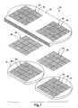
- Wafer-interposer assembly 10includes a multi wafer interposer 12 , an array 14 of conductive attachment elements 16 and an array 18 of conductive attachment elements 20 .
- Wafer-interposer assembly 10also includes a wafer 22 and a wafer 24 .
- Interposer 12has an array 26 of conductive contact pads 28 and an array 30 of conductive contact pads 32 on the upper surface thereof. Arrays 26 and 30 are each split into sixteen sections separated by dotted lines.
- interposer 12will be cut when interposer 12 is diced into chip assemblies, including a section of interposer 12 and an associated chip from either wafer 22 or 24 , as will be described in more detail below.
- arrays 26 and 30 of interposer 12are depicted as having sixteen sections in FIG. 1, this depiction is for simplicity and clarity of description as those skilled in the art will recognize that actual interposes will have several hundred or several thousand sections which correspond to the several hundred or several thousand chips on wafers 22 and 24 .
- Each of the sixteen sections of array 26has sixteen contact pads 28 and each of the sixteen sections of array 30 has sixteen contact pads 32 depicted therein.
- the contact pads 28 and 32represent the locations where interposer 12 will be electrically connected to a substrate once interposer 12 has been diced into chip assemblies, as will be described in more detail below. It should be noted that while array 26 is depicted as having sixteen contact pads 28 in each section and array 30 is depicted as having sixteen contact pads 32 in each section in FIG. 1, this depiction is for simplicity and clarity of description as those skilled in the art will recognize that the actual number of contact pads 28 and 32 in each section will be several hundred or several thousand contact pads.
- interposer 12On the lower surface of interposer 12 there are two similar arrays of conductive contact pads (not picture).
- the contact pads on the lower surface of interposer 12have the same geometry as contact pads 28 and contact pads 32 .
- the contact pads on the lower surface of interposer 12represent the locations where interposer 12 will be electrically connected to wafers 22 and 24 , as will be described in more detail below. It should be noted that the actual number of sections and the actual number of contact pads in each section on the lower surface of interposer 12 will be several hundred or several thousand instead of sixteen.
- Array 14 of conductive attachment elements 16is also split into sixteen sections separated by dotted lines. Each of the sections has sixteen conductive attachment elements 16 that correspond to the contact pads on the lower surface of interposer 12 below array 26 . Similarly, array 18 of conductive attachment elements 20 is split into sixteen sections separated by dotted lines. Each of the sections have sixteen conductive attachment elements 20 that correspond to the contact pads on the lower surface of interposer 12 below array 30 .
- Conductive attachment elements 16 and 20may be in the shape of balls, bumps, columns and the like. Conductive attachment elements 16 and 20 may be formed from any suitable electrically conductive material such as solder, including tin based solder, gold based solder, zinc based solder, indium based solder and the like. Alternatively, conductive attachment elements 16 and 20 may be formed from a conductive epoxy, a conductive polymer or the like. Conductive attachment elements 16 and 20 may be attached to interposer 12 by any number of attachment techniques including screening, flowing, molding, reflowing, dipping, electroplating, adhering and the like, depending upon which material is used for conductive attachment elements 16 and 20 .
- conductive attachment elements 16 and 20are the same size, shape and material. As such, conductive attachment elements 16 and 20 may be attached to interposer 12 using the same process. It should be noted by those skilled in the art that conductive attachment elements 16 may be a different size, a different shape, a different material or may be attached to interposer 12 using a different process than conductive attachment elements 20 without departing from the present invention.
- conductive attachment elements 16 of array 14electrically connect and mechanically bond contact pads 36 of each chip 34 to the facing contact pads on the lower surface of interposer 12 .
- conductive attachment elements 20 of array 18electrically connect and mechanically bond contact pads 40 of each chip 38 to the facing contact pads on the lower surface of interposer 12 .
- These permanent electrical and mechanical connectionsmay be achieved using, for example, a heating method such as reflowing or thermal compression.
- Wafer-interposer assembly 10also includes wafers 22 and 24 that are attached to the bottom surface of interposer 12 .
- Wafer 22has a plurality of chips 34 depicted thereon having dotted lines therebetween that represent the locations where wafer 22 will be cut when wafer 22 is diced into chip assemblies, as will be described in more detail below.
- Wafer 22is depicted as having sixteen chips 34 . This depiction is for simplicity and clarity of description as those skilled in the art will recognize that actual number of chips 34 on wafer 22 will be several hundred or several thousand.
- Each chip 34has a plurality of conductive contact pads 36 on its face.
- Each chip 34is depicted as having sixteen contact pads 36 , for simplicity and clarity of description, which correspond with one of the conductive attachment elements 16 in array 14 and represent the locations where chips 34 will be electrically connected to interposer 12 . It should be noted by those skilled in the art that the actual number of contact pads 36 on each chip 34 will be several hundred or several thousand instead of sixteen.
- wafer 24has a plurality of chips 38 depicted thereon having dotted lines therebetween that represent the locations where wafer 24 will be cut when wafer 24 is diced into chip assemblies, as will be described in more detail below.
- Wafer 24is depicted as having sixteen chips 38 . This depiction is for simplicity and clarity of description as those skilled in the art will recognize that actual number of chips 38 on wafer 24 will be several hundred or several thousand.
- Each chip 38has a plurality of conductive contact pads 40 on its face.
- Each chip 38is depicted as having sixteen contact pads 40 , for simplicity and clarity of description, which correspond with one of the conductive attachment elements 20 in array 18 and represent the locations where chips 38 will be electrically connected to interposer 12 . It should be noted by those skilled in the art that the actual number of contact pads 40 on each chip 38 will be several hundred or several thousand instead of sixteen.
- wafer-interposer assembly 10allows for the simultaneous testing of chips 34 of wafer 22 and chips 38 of wafer 24 . Simultaneous testing provides added efficiency to the testing process as numerous aspects of the functionality and performance of chips 34 and chips 38 may be tested. Importantly, this type of simultaneous testing allows for a determination of which chips 34 match up best with one another, which chips 38 match up best with one another and which chips 34 match up best with which chips 38 . This allows for optimization of the overall performance of specific matched sets as well as the overall performance of the lot of matched sets made from chips 34 and 38 .
- the matched setswill comprise two or more chips of the same type that may come from either wafer 22 or wafer 24 .
- these matched setsmay include multiple SRAM or DRAM components for use in a digital device, multiple amplifiers components for use in an analog device, multiple mixer, attenuator or circulator components for a RF device and the like.
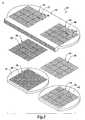
- Wafer-interposer assembly 50includes a multi wafer interposer 52 , an array 54 of conductive attachment elements 56 and an array 58 of conductive attachment elements 60 .
- Wafer-interposer assembly 50also includes a wafer 62 and a wafer 64 .
- Interposer 52has an array 66 of conductive contact pads 68 and an array 70 of conductive contact pads 72 on the upper surface thereof. Arrays 66 and 70 are each split into sixteen sections separated by dotted lines which represent the locations where interposer 52 will be diced.
- Each of the sixteen sections of array 66has sixteen contact pads 68 and each of the sixteen sections of array 70 has sixteen contact pads 72 depicted therein.
- the contact pads 68 and 72represent the locations where interposer 52 will be electrically connected to a substrate once interposer 52 has been diced.
- interposer 52On the lower surface of interposer 52 there are two arrays of conductive contact pads (not picture).
- the contact pads on the lower surface of interposer 52 below array 66have the same geometry as contact pads 68 .
- the contact pads on the lower surface of interposer 52 below array 70do not have the same geometry as contact pads 72 , as will be explained in greater detail below.
- Array 54 of conductive attachment elements 56is split into sixteen sections separated by dotted lines. Each of the sections has sixteen conductive attachment elements 56 that correspond to the contact pads on the lower surface of interposer 52 below array 66 .
- Array 58 of conductive attachment elements 60is split into sixteen sections separated by dotted lines. Each of the sections have thirty-six conductive attachment elements 60 that correspond to the contact pads on the lower surface of interposer 52 below array 70 .
- conductive attachment elements 56are depicted as being larger than conductive attachment elements 60 and having a larger pitch. Conductive attachment elements 56 and 60 are of the same shape and preferably are of the same material such that conductive attachment elements 56 and 60 may be attached to interposer 52 using the same process, however, this is not a requirement of the present invention.
- Wafers 62 and 64are attached to the bottom surface of interposer 52 .
- Wafer 62has a plurality of chips 74 depicted thereon having dotted lines therebetween that represent the locations where wafer 62 will be diced.
- Each chip 74has a plurality of conductive contact pads 76 on its face.
- Each chip 74is depicted as having sixteen contact pads 76 , which correspond with one of the conductive attachment elements 56 in array 54 and represent the locations where chips 74 will be electrically connected to interposer 52 .
- wafer 64has a plurality of chips 78 depicted thereon having dotted lines therebetween that represent the locations where wafer 64 will be diced. Wafer 64 is depicted as having sixteen chips 78 . Each chip 78 has a plurality of conductive contact pads 80 on its face. Each chip 78 is depicted as having thirty-six contact pads 80 , which correspond with the conductive attachment elements 60 in array 58 and represent the locations where chips 78 will be electrically connected to interposer 52 .
- chips 74 of wafer 62are of a different type than chips 78 of wafer 64 .
- wafer-interposer assembly 50allows for the simultaneous testing of different types of chips 74 and 78 from the two wafers 62 and 64 which provides significant efficiency gains over prior art testing scenarios.
- the functionality and performance of one or more chips 74 and one or more chips 78may be tested simultaneously to determine whether specific chips 74 match well with specific chips 78 so that matched sets containing chips 74 and 78 may be assembled.
- these matched setsmay include a controller and multiple amplifiers, a RF mixer and a DSP, an ASIC component and multiple SRAMs as well as enumerable other desirable component combinations.
- interposer 52includes a plurality of layers having routing lines and vias therein which serve as electrical conductors.
- One set of conductorsdepicted as conductors 90 , 92 and 94 , pass through interposer 52 and serve to electrically connect pads 76 of chips 74 to the contact pads 68 of interposer 52 .
- Conductors 90 , 92 and 94are selected to have suitable conductivity and may be, for example, copper.
- Interposer 52also includes a set of testing conductors, depicted as conductor 96 , that pass through interposer 52 connecting some of the contact pads 76 of chips 74 to a testing apparatus as will be explained in greater detail below.
- the testing conductorsmay provide direct electrical connection to the testing apparatus or may pass through a multiplexer or other intervening apparatus (not shown) incorporated into interposer 52 .
- contact pads 76 of chips 74 and contact pads 68 of interposer 52have identical geometries.
- the present inventionis by no means limited to having identical geometries.
- one of the advantages of the present inventionis that the contact pads on the upper surface of interposer 52 may utilize a geometry that is different from that of the contact pads of the chips.
- chip designershave been limited in chip layout in that all connections between the elements of a chip and the outside world had to be made either through the peripheral edges of the chip (for wire bonding) or at least through a standard pin or pad layout defined by a standardization body, such as the Joint Electrical Dimensional Electronic Committee (JEDEC). The interconnection requirements, therefore, have traditionally driven the chip layout.
- Chip designs for use with an interposer of the present inventionare not limited by such constraints.
- Wafer-interposer assembly 110includes a multi wafer interposer 112 , an array 114 of conductive attachment elements 116 and an array 118 of conductive attachment elements 120 .
- Wafer-interposer assembly 110also includes a wafer 122 and a wafer 124 .
- Interposer 112has an array 126 of conductive contact pads 128 and an array 130 of conductive contact pads 132 on the upper surface thereof.
- Array 126is each split into sixteen sections separated by dotted lines which represent the locations where interposer 122 will be diced.
- array 130is each split into four sections separated by dotted lines which represent the locations where interposer 122 will be diced.
- Each of the sixteen sections of array 126has sixteen contact pads 128 .
- Each of the four sections of array 130has thirty-six contact pads 132 depicted therein.
- the contact pads 128 and 132represent the locations where interposer 112 will be electrically connected to a substrate once interposer 112 has been diced.
- interposer 52On the lower surface of interposer 52 there are two arrays of conductive contact pads (not picture).
- the contact pads on the lower surface of interposer 112 below array 126have the same geometry as contact pads 128 and the contact pads on the lower surface of interposer 122 below array 130 have the same geometry as contact pads 132 .
- Array 114 of conductive attachment elements 116is split into sixteen sections separated by dotted lines. Each of the sections has sixteen conductive attachment elements 116 that correspond to the contact pads on the lower surface of interposer 112 below array 126 .
- Array 118 of conductive attachment elements 120is split into four sections separated by dotted lines. Each of the sections have thirty-six conductive attachment elements 120 that correspond to the contact pads on the lower surface of interposer 112 below array 130 .
- conductive attachment elements 120are depicted as being larger than conductive attachment elements 116 and having a larger pitch.
- Conductive attachment elements 116 and 120are of the same shape and preferably are of the same material such that conductive attachment elements 116 and 120 may be attached to interposer 112 using the same process, however, this is not a requirement of the present invention.
- Wafers 122 and 124are attached to the bottom surface of interposer 112 .
- Wafer 122has a plurality of chips 134 depicted thereon having dotted lines therebetween that represent the locations where wafer 122 will be diced.
- Each chip 134has a plurality of conductive contact pads 136 on its face.
- Each chip 134is depicted as having sixteen contact pads 136 , which correspond with one of the conductive attachment elements 116 in array 114 and represent the locations where chips 134 will be electrically connected to interposer 112 .
- wafer 124has a plurality of chips 138 depicted thereon having dotted lines therebetween that represent the locations where wafer 134 will be diced.
- Wafer 134is depicted as having four chips 138 .
- Each chip 138has a plurality of conductive contact pads 140 on its face.
- Each chip 138is depicted as having thirty-six contact pads 140 , which correspond with the conductive attachment elements 120 in array 118 and represent the locations where chips 138 will be electrically connected to interposer 112 .
- chips 134 of wafer 122are of a different type than chips 138 of wafer 124 .
- wafer-interposer assembly 110allows for the simultaneous testing of different types of chips 134 and 138 from the two wafers 122 and 124 which provides significant efficiency gains over prior art testing scenarios. Specifically, the functionality and performance of one or more chips 134 and one or more chips 138 may be tested simultaneously to determined whether specific chips 134 match well with specific chips 138 .
- FIG. 5therein is depicted a wafer-interposer assembly 150 of the present invention.
- Wafer-interposer assembly 150includes a multi wafer interposer 152 , an array 154 of conductive attachment elements 156 , an array 158 of conductive attachment elements 160 , an array 162 of conductive attachment elements 164 and an array 166 of conductive attachment elements 168 .
- Wafer-interposer assembly 150also includes wafers 170 , 172 , 174 and 176 .
- Interposer 152has four arrays 178 , 180 , 182 and 184 of conductive contact pads 186 , 188 , 190 and 192 , respectively, on the upper surface thereof.
- Arrays 178 , 180 , 182 and 184are each split into sixteen sections separated by dotted lines which represents the locations where interposer 152 will be diced.
- Each of the sixteen sections of arrays 178 , 180 , 182 and 184have sixteen contact pads 186 , 188 , 190 and 192 , respectively.
- Contact pads 186 , 188 , 190 and 192represent the locations where interposer 152 will be electrically connected to a substrate once interposer 152 has been diced.
- interposer 152On the lower surface of interposer 152 there are four arrays of conductive contact pads (not picture). In the illustrated embodiment, the contact pads on the lower surface of interposer 152 below arrays 178 , 180 , 182 and 184 have the same geometries as contact pads 186 , 188 , 190 and 192 .
- Arrays 154 , 158 , 162 and 166 of conductive attachment elements 156 , 160 , 164 and 168 , respectively,are each split into sixteen sections separated by dotted lines. Each of the sections has sixteen conductive attachment elements therein that correspond to contact pads on the lower surface of interposer 152 .
- Wafers 170 , 172 , 174 and 176are attached to the bottom surface of interposer 152 .
- Wafers 170 , 172 , 174 and 176each have a plurality of chips 194 , 196 , 198 and 200 , respectively, depicted thereon having dotted lines therebetween that represent the locations where wafers 170 , 172 , 174 and 176 will be diced.
- Each chip 194 , 196 , 198 and 200has a plurality of conductive contact pads 202 , 204 , 206 and 208 , respectively, on its face.
- Each chip 194 , 196 , 198 and 200is depicted as having sixteen contact pads 202 , 204 , 206 and 208 , respectively, each of which correspond with one of the conductive attachment elements in arrays 154 , 158 , 162 and 166 and represent the locations where chips 194 , 196 , 198 and 200 will be electrically connected to interposer 152 .
- each of the chips 194 , 196 , 198 and 200 on the various wafers 170 , 172 , 174 and 176are of the same type.
- wafer-interposer assembly 150allows for the simultaneous testing chips 194 , 196 , 198 and 200 on all four wafers 170 , 172 , 174 and 176 which provides significant efficiency gains over prior art testing scenarios.
- an interposerthat accommodates four wafers could alternatively be used to simultaneously test wafers that have different types of chips thereon.
- an interposers of the present inventionmay accommodate and be used to test other numbers of wafers, either greater than or less than that depicted herein without departing from the principles of the present invention.
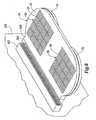
- wafer-interposer assembly 10 of FIG. 1connected to a testing unit 220 .
- Wafer-interposer assembly 10interfaces with testing unit 220 through a testing connector 222 the comprising a plurality of testing contacts 224 , shown here as pins.
- the testing contacts 224 of the testing connector 220connect with the testing sockets of testing connector 226 of wafer-interposer assembly 10
- wafer-interposer assembly 10can be used to run chips 36 and 38 (see FIG. 1) on wafers 22 and 24 through any number of tests including a complete parametric test, a burn-on or whatever subsets thereof are deemed necessary for that particular chip design.
- signalsmay be sent to chips 36 and 38 to test each function of the chips which may ideally occur across a range of conditions, so as to simulate real world operation.
- Testing unit 220may incorporate a heating and cooling apparatus for testing the chips across a range of temperatures.
- Testing unit 220may also incorporate a device for vibrating or otherwise mechanically stressing chips 36 and 38 .
- wafer-interposer assembly 10 of the present inventionmay be used to select chips 34 and 38 from each of the wafers 22 and 24 that will be used in a matched set of chips.
- the testingmay include performance tests over a range of temperatures, testing for leakage currents, testing for offset voltages and the like to determine which chips 34 from wafer 22 could be included in a matched set with which chips 38 from wafer 24 to achieve optimum performance.
- the testingmay result in giving chips 34 and 38 of wafers 22 and 24 a grade for speed or other performance characteristics such that chips 34 of a particular grade may be matched with chips 38 of that same grade.
- the testingmay result in a non-conformance or mismatch determination wherein certain chips 34 may not be matched with certain chips 38 .
- Certain chips 34may alternatively be designated as incompatible with any chips 38 .
- FIG. 6has been described as testing wafer-interposer assembly 10 of FIG. 1 wherein chips 34 and 38 are of the same type, it should be understood by those skilled in the art that the same testing procedures will be followed when the chips of the two wafers are of different types, such as using wafer-interposer assembly 50 of FIG. 2 or wafer-interposer assembly 110 of FIG. 4. Likewise, it should be understood by those skilled in the art that the same testing procedures will also be followed when more than two wafers are being tested simultaneously, such as when using wafer-interposer assembly 150 of FIG. 5.
- wafer-interposer assembly 10 of FIG. 1is depicted including an array 230 of conductive attachment elements 232 and an array 234 of conductive attachment elements 236 .
- Array 230is split into sixteen sections separated by dotted lines. Each of the sections has sixteen conductive attachment elements 232 that correspond to contact pads 28 of array 26 on interposer 12 .
- array 234 of conductive attachment elements 236is split into sixteen sections separated by dotted lines. Each of the sections have sixteen conductive attachment elements 236 that correspond to contact pads 32 of array 34 on interposer 12 .
- conductive attachment elements 232 and 236are the same size, shape and material. As such, conductive attachment elements 232 and 236 may be attached to interposer 12 using the same process. It should be noted by those skilled in the art that conductive attachment elements 232 may be a different size, a different shape, a different material or may be attached to interposer 12 using a different process than conductive attachment elements 236 without departing from the present invention.
- conductive attachment elements 232 and 236will be used to electrically connect and mechanically bond a diced section of wafer-interposer assembly 10 , including a section of interposer 12 and its associated chip 34 or 36 to a substrate as will be explained in more detail below.
- These permanent electrical and mechanical connectionsmay be achieved using, for example, a heating method such as reflowing or thermal compression.
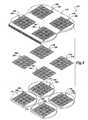
- FIG. 8shows an array 240 of chip assemblies 242 and an array 244 of chip assemblies 246 after singulation of a wafer-interposer assembly of the present invention.
- Each chip assembly 242comprises a chip 248 , a section 250 of the interposer and a plurality of conductive attachment elements 252 disposed on conductive contact pads 254 on the exposed surface of chip assemblies 242 .
- each chip assembly 246comprises a chip 256 , a section 258 of the interposer and a plurality of conductive attachment elements 260 disposed on conductive contact pads 262 on the exposed surface of chip assemblies 246 .
- Chip assemblies 242 and 246may, for example, include chips of the same type, such as those diced from wafer-interposer assembly 10 of FIG. 1, or may contain chips of different types such as those diced from wafer-interposer assembly 50 of FIG. 2.
- a chip assembly 242 and a chip assembly 246may be mounted together on a substrate 264 as a matched set.
- Substrate 264has a plurality of conductive layers 266 and dielectric layers 268 .
- Chip assemblies 242 and 246are electrically and mechanically attached to contact pads on the surface of substrate 264 through conductive attachment elements 252 and 260 , respectively.
- the diced sections 250 and 258 of the interposerprovide electrical connection between chips 248 and 256 and substrate 264 .
- substrate 264may be a traditional FR4 circuit board.
- substrate 264may be composed of a higher grade material such as a ceramic, which is typically used in multichip packages.
- FIG. 10therein is depicted an array 280 of chip assemblies, including chip assemblies 282 , 284 , 286 and 288 , after dicing a wafer-interposer assembly of the present invention.
- An array 290 of chip assemblies 292is also depicted.
- Each chip assembly 282 , 284 , 286 and 288includes a chip, a section of the interposer and a plurality of conductive attachment elements disposed on conductive pads on the exposed surfaces thereof.
- chip assembly 288includes a chip 294 , a section 296 of the interposer and a plurality of conductive attachment elements 298 disposed on conductive pads 300 .
- Chip assembly 292includes a chip 302 , a section 304 of the interposer and a plurality of conductive attachment elements 306 disposed on conductive pads 308 .
- chip assemblies 282 , 284 , 286 and 288contain chips of different type than chip assembly 292 such as those diced from wafer-interposer assembly 110 of FIG. 4.
- chip assemblies 282 , 284 , 286 and 288may be amplifiers while chip assembly 292 may be a controller.
- a matched set of componentsmay be mounted on a substrate 310 that has a plurality of conductive layers 312 and dielectric layers 314 .
- chip assemblies 282 , 284 , 286 and 288may be mounted together on a substrate 310 with chip assembly 292 .
- Chip assemblies 282 , 284 , 286 and 288are electrically and mechanically attached to contact pads on the surface of substrate 310 through conductive attachment elements 298 .
- chip assembly 292is electrically and mechanically attached to contact pads on the surface of substrate 310 through conductive attachment elements 306 .
- the diced sections of the interposerprovide electrical connection between substrate 310 and chips 294 of chip assemblies 282 , 284 , 286 and 288 and chip 302 of chip assembly 292 .
- FIGS. 9 and 11have depicted the matched sets of component as including two chip assemblies and five chip assemblies, respectively, it should be understood by those skilled in the art that any number of chip assemblies may be utilized in such a matched set. The specific number of chip assemblies will be selected based upon the desired functionality of the matched set.
- the testing process of the present inventionprovides for each of the components of a matched set, regardless of the number, to be tested together as part of a single wafer-interposer assembly. As such, the components for matched set are selected to be assembled together only after successful testing.
Landscapes
- Engineering & Computer Science (AREA)
- Microelectronics & Electronic Packaging (AREA)
- Power Engineering (AREA)
- Computer Hardware Design (AREA)
- Manufacturing & Machinery (AREA)
- Physics & Mathematics (AREA)
- Condensed Matter Physics & Semiconductors (AREA)
- General Physics & Mathematics (AREA)
- Testing Or Measuring Of Semiconductors Or The Like (AREA)
- Tests Of Electronic Circuits (AREA)
Abstract
Description
- This is a divisional application of co-pending application Ser. No. 09/629,309, entitled Method for Selecting Components for a Matched Set Using a Multi Wafer Interposer, filed on Jul. 31, 2000.[0001]
- The present invention relates in general to integrated circuits and, more particularly, to wafer level testing and selection of system components for a match set using an interposer that accommodates multiple wafers containing the component parts of the matched set.[0002]
- Modern electronic devices utilize semiconductor chips, commonly referred to as integrated circuits, which incorporate numerous electronic elements. These chips are mounted on substrates which physically support the chips and electrically interconnect the chips with other elements of the circuit. Such substrates may then be secured to an external circuit board or chassis.[0003]
- The size of the chips and substrate assembly is a major concern in modern electronic product design. The size of each subassembly influences the size of the overall electronic device. Moreover, the size of each subassembly controls the required distance between each chip and between chips and other elements of the circuit. Delays in transmission of electrical signals between chips are directly related to these distances. These delays limit the speed of operation of the device. Thus, more compact interconnection assemblies, with smaller distances between chips and smaller signal transmission delays, can permit faster operations.[0004]
- One approach for improving overall system performance is through the use of matched sets. For example, several identical or dissimilar components that have been identified by the individual testing phase of component processing to have certain performance tracking characteristics may be assembled together as a matched set. The components of such a matched sets are frequently attached to a single substrate in close proximity to one another. This strategy improves performance compared to conventional or non-optimized systems by reducing the overall space needed to accommodate the chips and by, among other things, shortening the distance between chips. Specifically, interconnect inductance and signal transmission delays are all reduced.[0005]
- One type of matched set includes a collection of identical components which have been identified to meet specific system performance requirements. For example, radio frequency (RF) systems often employ identical filters, switches, power dividers, mixers and high frequency amplifiers. Typically, each of the identical components has been extensively tested individually prior to inclusion in this type of system. The individual characterization tests for a filter, for instance, might measure insertion loss and phase shift as a function of frequency, input power and temperature. These multi-dimensional arrays of data are then compared to each other to identify individual components that perform within acceptable limits relative to each other. Components that are found to exhibit similar behavior under the various input stimuli will constitute a matched set of identical devices. Conversely, components that are found to exhibit dissimilar behavior under the various input stimuli, for example, the gain of one component having a negative slope over temperature while the gain of another component having a positive slope over temperature, will constitute a mismatch of components that will not be placed in a chip collection.[0006]
- Another type of matched set includes components of different device types that are combined such that the aggregate, cascaded performance meets system specifications. Mixed signal systems, for example, often utilize digital-to-analog (DAC) converters along with operational amplifiers (OpAmp) to process data. The performance of a product can often be improved by pairing a DAC with an OpAmp of similar performance. That is, the input characteristics of the OpAmp are optimized to match the output characteristics of the DAC. As in the case of the matched set of identical components described above, the component of a matched set of different components are also identified by comparing multi-dimensional arrays of data to each other to identify individual components that perform within acceptable limits relative to each other. Components that are found to exhibit similar behavior under the various input stimuli will form a matched set of different components while components that are found to exhibit dissimilar behavior under the various input stimuli are not placed in a chip collection due to the mismatch.[0007]
- It has been found, however, the certain mismatches are not identified when the components are tested individually. In fact, certain mismatches are not identified until the entire chip collection is assembled and the components are tested together for the first time. As such, some chip collections must be disassembled so that the valuable components may be, for example, packaged as individual components, while other chip collections are simple discarded.[0008]
- Therefore, a need has arisen for an improved method for selection of system components for a matched set. A need has also arisen for such a method that does not require elaborate data reduction of test results from individually tested components. Additionally, a need has arisen for such a method that allows for testing of the individual components together prior to the assembly of the matched set.[0009]
- The present invention disclosed herein provides a chip collection, known as a matched set, that maximizes system performance by selecting well matched integrated circuit chips for assembly together into the matched set. The present invention achieves this result by allowing for testing of the various integrated circuit chips together prior to the assembly of the matched set. This testing utilizes a wafer level interposer that accommodates multiple wafers that contain all of the chips to be included in the matched set. This combination is referred to as a wafer-interposer assembly. In the present invention, this wafer-interposer assembly is diced into a plurality of chip assemblies that are assembled into the matched set.[0010]
- In its broadest form, the present invention provides for the attachment of two semiconductor wafers each having a plurality of integrated circuit chips thereon to the interposer for testing of the integrated circuit chips. The integrated circuit chips of the first wafer may be of the same type as the integrated circuit chips of the second wafer, such as DRAM chips. Alternatively, the integrated circuit chips of the first wafer may be of a different type from the integrated circuit chips of the second wafer. For example, the integrated circuit chips of the first wafer may be amplifiers while the integrated circuit chips of the second wafer may be controllers. Likewise, the integrated circuit chips of the first wafer may carry the same type of signal as the integrated circuit chips of the second wafer, such as analog signals for an amplifier. Alternatively, the integrated circuit chips of the first wafer may carry a different type of signal than the integrated circuit chips of the second wafer. For example, the integrated circuit chips of the first wafer may be mixers that carry RF signals while the integrated circuit chips of the second wafer may be DSPs that carry digital signals.[0011]
- Prior to testing, the two wafers are electrically and mechanically coupling to the interposer such that the wafer-interposer assembly may be connected to a testing apparatus. The testing may include performance tests over a range of temperatures, testing for leakage currents, testing for offset voltages and the like to determine which integrated circuit chips from the first wafer could be included in a matched set with particular integrated circuit chips from the second wafer to achieve optimum performance. Likewise, the testing may include grading of the integrated circuit chips of the first wafer and the second wafer for speed or other performance characteristics such that the integrated circuit chips of the first wafer that receive a particular grade are matched with integrated circuit chips from the second wafer having a similar grade. Additionally, the testing may include testing for non-conformance wherein certain integrated circuit chips of the first wafer may not be matched with any integrated circuit chips of the second wafer.[0012]
- Once testing is complete, the wafer-interposer assembly may be diced into a plurality of chip assemblies having chips of the first wafer and a plurality of chip assemblies having chips of the second wafer. One of the chip assemblies having a chip from the first wafer may them be matched with one of the chip assemblies having a chip from the second wafer, for inclusion in a matched set. This selection is based upon the results of the testing of the integrated circuit chips of the first wafer and the integrated circuit chips of the second wafer. Alternatively, more than one of the chip assemblies having chips from the first wafer may be matched with one or more chip assemblies having chips from the second wafer for inclusion in a matched set.[0013]
- Using this process, all or substantially all of the integrated circuit chips from one wafer may be matched with one or more of the integrated circuit chips of a second wafer based upon the desired performance characteristics of the matched set that will contain these devices. By performing the testing prior to assembly of the matched set, the performance characteristics of each of the matched sets assembled using integrated circuit chips of the first and second wafers are enhanced as is the overall performance of the entire lot of matched set devices.[0014]
- For a more complete understanding of the features and advantages of the present invention, reference is now made to the detailed description of the invention along with the accompanying figures in which corresponding numerals in the different figures refer to corresponding parts and in which:[0015]
- FIG. 1 is an exploded view of a wafer-interposer assembly of the present invention including two wafers having chips of the same type;[0016]
- FIG. 2 is an exploded view of a wafer-interposer assembly of the present invention including two wafers having chips of different types;[0017]
- FIGS.[0018]3A-3B are cross sectional views taken respectively along
line 3A-3A and3B-3B of FIG. 2; - FIG. 4 is an exploded view of a wafer-interposer assembly of the present invention including two wafers having chips of different types;[0019]
- FIG. 5 is an exploded view of a wafer-interposer assembly of the present invention including four wafers having chips of the same type;[0020]
- FIG. 6 is an isometric view of a wafer-interposer assembly of the present invention, being inserted into a testing apparatus;[0021]
- FIG. 7 is an exploded view of a wafer-interposer assembly of the present invention;[0022]
- FIG. 8 is an isometric view of a plurality of chip assemblies after singulation of a wafer-interposer assembly of the present invention;[0023]
- FIG. 9 is an isometric view of a matched set of chip assemblies of the present invention having chips from different wafers in place on a substrate;[0024]
- FIG. 10 is an isometric view of a plurality of chip assemblies after singulation of a wafer-interposer assembly of the present invention; and[0025]
- FIG. 11 is an isometric view of a matched set of chip assemblies of the present invention including chips of different types in place on a substrate.[0026]
- While the making and using of various embodiments of the present invention are discussed in detail below, it should be appreciated that the present invention provides many applicable inventive concepts which can be embodied in a wide variety of specific contexts. The specific embodiments discussed herein are merely illustrative of specific ways to make and use the invention and do not define the scope of the invention.[0027]
- The general features of a wafer-interposer assembly of the present invention are shown in FIG. 1 and are generally designated[0028]10. Wafer-
interposer assembly 10 includes amulti wafer interposer 12, anarray 14 ofconductive attachment elements 16 and anarray 18 ofconductive attachment elements 20. Wafer-interposer assembly 10 also includes awafer 22 and awafer 24.Interposer 12 has anarray 26 ofconductive contact pads 28 and anarray 30 ofconductive contact pads 32 on the upper surface thereof.Arrays interposer 12 will be cut wheninterposer 12 is diced into chip assemblies, including a section ofinterposer 12 and an associated chip from eitherwafer arrays interposer 12 are depicted as having sixteen sections in FIG. 1, this depiction is for simplicity and clarity of description as those skilled in the art will recognize that actual interposes will have several hundred or several thousand sections which correspond to the several hundred or several thousand chips onwafers - Each of the sixteen sections of[0029]
array 26 has sixteencontact pads 28 and each of the sixteen sections ofarray 30 has sixteencontact pads 32 depicted therein. Thecontact pads interposer 12 will be electrically connected to a substrate onceinterposer 12 has been diced into chip assemblies, as will be described in more detail below. It should be noted that whilearray 26 is depicted as having sixteencontact pads 28 in each section andarray 30 is depicted as having sixteencontact pads 32 in each section in FIG. 1, this depiction is for simplicity and clarity of description as those skilled in the art will recognize that the actual number ofcontact pads - On the lower surface of[0030]
interposer 12 there are two similar arrays of conductive contact pads (not picture). In the illustrated embodiment, the contact pads on the lower surface ofinterposer 12 have the same geometry ascontact pads 28 andcontact pads 32. As such, there are two arrays each having sixteen sections with sixteen contact pads on the lower surface ofinterposer 12. The contact pads on the lower surface ofinterposer 12 represent the locations whereinterposer 12 will be electrically connected towafers interposer 12 will be several hundred or several thousand instead of sixteen. Also, it should be noted that directional terms, such as “above,” “below,” “upper,” “lower,” etc., are used for convenience in referring to the accompanying drawings as it is to be understood that the various embodiments of the present invention described herein may be utilized in various orientations, such as inclined, inverted, horizontal, vertical, etc., without departing from the principles of the present invention. - [0031]
Array 14 ofconductive attachment elements 16 is also split into sixteen sections separated by dotted lines. Each of the sections has sixteenconductive attachment elements 16 that correspond to the contact pads on the lower surface ofinterposer 12 belowarray 26. Similarly,array 18 ofconductive attachment elements 20 is split into sixteen sections separated by dotted lines. Each of the sections have sixteenconductive attachment elements 20 that correspond to the contact pads on the lower surface ofinterposer 12 belowarray 30. - [0032]
Conductive attachment elements Conductive attachment elements conductive attachment elements Conductive attachment elements conductive attachment elements conductive attachment elements conductive attachment elements conductive attachment elements 16 may be a different size, a different shape, a different material or may be attached to interposer12 using a different process thanconductive attachment elements 20 without departing from the present invention. - After assembly,[0033]
conductive attachment elements 16 ofarray 14 electrically connect and mechanically bondcontact pads 36 of eachchip 34 to the facing contact pads on the lower surface ofinterposer 12. Likewise,conductive attachment elements 20 ofarray 18 electrically connect and mechanically bondcontact pads 40 of eachchip 38 to the facing contact pads on the lower surface ofinterposer 12. These permanent electrical and mechanical connections may be achieved using, for example, a heating method such as reflowing or thermal compression. - Wafer-[0034]
interposer assembly 10 also includeswafers interposer 12.Wafer 22 has a plurality ofchips 34 depicted thereon having dotted lines therebetween that represent the locations wherewafer 22 will be cut whenwafer 22 is diced into chip assemblies, as will be described in more detail below.Wafer 22 is depicted as having sixteenchips 34. This depiction is for simplicity and clarity of description as those skilled in the art will recognize that actual number ofchips 34 onwafer 22 will be several hundred or several thousand. - Each[0035]
chip 34 has a plurality ofconductive contact pads 36 on its face. Eachchip 34 is depicted as having sixteencontact pads 36, for simplicity and clarity of description, which correspond with one of theconductive attachment elements 16 inarray 14 and represent the locations wherechips 34 will be electrically connected tointerposer 12. It should be noted by those skilled in the art that the actual number ofcontact pads 36 on eachchip 34 will be several hundred or several thousand instead of sixteen. - Likewise,[0036]
wafer 24 has a plurality ofchips 38 depicted thereon having dotted lines therebetween that represent the locations wherewafer 24 will be cut whenwafer 24 is diced into chip assemblies, as will be described in more detail below.Wafer 24 is depicted as having sixteenchips 38. This depiction is for simplicity and clarity of description as those skilled in the art will recognize that actual number ofchips 38 onwafer 24 will be several hundred or several thousand. - Each[0037]
chip 38 has a plurality ofconductive contact pads 40 on its face. Eachchip 38 is depicted as having sixteencontact pads 40, for simplicity and clarity of description, which correspond with one of theconductive attachment elements 20 inarray 18 and represent the locations wherechips 38 will be electrically connected tointerposer 12. It should be noted by those skilled in the art that the actual number ofcontact pads 40 on eachchip 38 will be several hundred or several thousand instead of sixteen. - As such, wafer-[0038]
interposer assembly 10 allows for the simultaneous testing ofchips 34 ofwafer 22 andchips 38 ofwafer 24. Simultaneous testing provides added efficiency to the testing process as numerous aspects of the functionality and performance ofchips 34 andchips 38 may be tested. Importantly, this type of simultaneous testing allows for a determination of which chips34 match up best with one another, which chips38 match up best with one another and which chips34 match up best with which chips38. This allows for optimization of the overall performance of specific matched sets as well as the overall performance of the lot of matched sets made fromchips wafer 22 orwafer 24. For example, these matched sets may include multiple SRAM or DRAM components for use in a digital device, multiple amplifiers components for use in an analog device, multiple mixer, attenuator or circulator components for a RF device and the like. - Referring now to FIG. 2, therein is depicted a wafer-[0039]
interposer assembly 50 of the present invention. Wafer-interposer assembly 50 includes amulti wafer interposer 52, anarray 54 ofconductive attachment elements 56 and anarray 58 ofconductive attachment elements 60. Wafer-interposer assembly 50 also includes awafer 62 and awafer 64.Interposer 52 has anarray 66 ofconductive contact pads 68 and anarray 70 ofconductive contact pads 72 on the upper surface thereof.Arrays interposer 52 will be diced. - Each of the sixteen sections of[0040]
array 66 has sixteencontact pads 68 and each of the sixteen sections ofarray 70 has sixteencontact pads 72 depicted therein. Thecontact pads interposer 52 will be electrically connected to a substrate onceinterposer 52 has been diced. - On the lower surface of[0041]
interposer 52 there are two arrays of conductive contact pads (not picture). In the illustrated embodiment, the contact pads on the lower surface ofinterposer 52 belowarray 66 have the same geometry ascontact pads 68. The contact pads on the lower surface ofinterposer 52 belowarray 70, however, do not have the same geometry ascontact pads 72, as will be explained in greater detail below. - [0042]
Array 54 ofconductive attachment elements 56 is split into sixteen sections separated by dotted lines. Each of the sections has sixteenconductive attachment elements 56 that correspond to the contact pads on the lower surface ofinterposer 52 belowarray 66.Array 58 ofconductive attachment elements 60 is split into sixteen sections separated by dotted lines. Each of the sections have thirty-sixconductive attachment elements 60 that correspond to the contact pads on the lower surface ofinterposer 52 belowarray 70. In the illustrated embodiment,conductive attachment elements 56 are depicted as being larger thanconductive attachment elements 60 and having a larger pitch.Conductive attachment elements conductive attachment elements - [0043]
Wafers interposer 52.Wafer 62 has a plurality ofchips 74 depicted thereon having dotted lines therebetween that represent the locations wherewafer 62 will be diced. Eachchip 74 has a plurality ofconductive contact pads 76 on its face. Eachchip 74 is depicted as having sixteencontact pads 76, which correspond with one of theconductive attachment elements 56 inarray 54 and represent the locations wherechips 74 will be electrically connected tointerposer 52. - Likewise,[0044]
wafer 64 has a plurality ofchips 78 depicted thereon having dotted lines therebetween that represent the locations wherewafer 64 will be diced.Wafer 64 is depicted as having sixteenchips 78. Eachchip 78 has a plurality ofconductive contact pads 80 on its face. Eachchip 78 is depicted as having thirty-sixcontact pads 80, which correspond with theconductive attachment elements 60 inarray 58 and represent the locations wherechips 78 will be electrically connected tointerposer 52. - In the illustrated embodiment, chips[0045]74 of
wafer 62 are of a different type thanchips 78 ofwafer 64. As such, wafer-interposer assembly 50 allows for the simultaneous testing of different types ofchips wafers more chips 74 and one ormore chips 78 may be tested simultaneously to determine whetherspecific chips 74 match well withspecific chips 78 so that matchedsets containing chips - Referring next to FIGS. 3A and 3B, cross sectional views of wafer-[0046]
interposer assembly 50 taken alonglines 3A-3A and3B-3B are depicted. As best seen in FIG. 3A,interposer 52 includes a plurality of layers having routing lines and vias therein which serve as electrical conductors. One set of conductors, depicted asconductors interposer 52 and serve to electrically connectpads 76 ofchips 74 to thecontact pads 68 ofinterposer 52.Conductors Interposer 52 also includes a set of testing conductors, depicted asconductor 96, that pass throughinterposer 52 connecting some of thecontact pads 76 ofchips 74 to a testing apparatus as will be explained in greater detail below. The testing conductors may provide direct electrical connection to the testing apparatus or may pass through a multiplexer or other intervening apparatus (not shown) incorporated intointerposer 52. - As seen in FIG. 3A,[0047]
contact pads 76 ofchips 74 andcontact pads 68 ofinterposer 52 have identical geometries. The present invention, however, is by no means limited to having identical geometries. As each die design may have unique pad geometry, one of the advantages of the present invention is that the contact pads on the upper surface ofinterposer 52 may utilize a geometry that is different from that of the contact pads of the chips. Traditionally, chip designers have been limited in chip layout in that all connections between the elements of a chip and the outside world had to be made either through the peripheral edges of the chip (for wire bonding) or at least through a standard pin or pad layout defined by a standardization body, such as the Joint Electrical Dimensional Electronic Committee (JEDEC). The interconnection requirements, therefore, have traditionally driven the chip layout. Chip designs for use with an interposer of the present invention are not limited by such constraints. - For example, as best seen in FIG. 3B,[0048]
interposer 52 includes a plurality of layers having routing lines and vias therein which serve as electrical conductors. One set of conductors, depicted asconductors interposer 52 to electrically connectcontact pads 72 on the upper surface ofinterposer 52 to contactpads 80 onchips 78. Another set of conductors, depicted asconductors interposer 52 and are used to connectcertain pads 80 ofchips 78 to a testing apparatus, as will be explained in greater detail below. As such, the geometry ofpads 72 on the upper surface ofinterposer 52 may be different from that ofpads 80 onchips 78. - Referring now to FIG. 4, therein is depicted a wafer-[0049]
interposer assembly 110 of the present invention. Wafer-interposer assembly 110 includes amulti wafer interposer 112, anarray 114 ofconductive attachment elements 116 and anarray 118 ofconductive attachment elements 120. Wafer-interposer assembly 110 also includes awafer 122 and awafer 124.Interposer 112 has anarray 126 ofconductive contact pads 128 and anarray 130 ofconductive contact pads 132 on the upper surface thereof.Array 126 is each split into sixteen sections separated by dotted lines which represent the locations whereinterposer 122 will be diced. Likewise,array 130 is each split into four sections separated by dotted lines which represent the locations whereinterposer 122 will be diced. - Each of the sixteen sections of[0050]
array 126 has sixteencontact pads 128. Each of the four sections ofarray 130 has thirty-sixcontact pads 132 depicted therein. Thecontact pads interposer 112 will be electrically connected to a substrate onceinterposer 112 has been diced. - On the lower surface of[0051]
interposer 52 there are two arrays of conductive contact pads (not picture). In the illustrated embodiment, the contact pads on the lower surface ofinterposer 112 belowarray 126 have the same geometry ascontact pads 128 and the contact pads on the lower surface ofinterposer 122 belowarray 130 have the same geometry ascontact pads 132. - [0052]
Array 114 ofconductive attachment elements 116 is split into sixteen sections separated by dotted lines. Each of the sections has sixteenconductive attachment elements 116 that correspond to the contact pads on the lower surface ofinterposer 112 belowarray 126.Array 118 ofconductive attachment elements 120 is split into four sections separated by dotted lines. Each of the sections have thirty-sixconductive attachment elements 120 that correspond to the contact pads on the lower surface ofinterposer 112 belowarray 130. In the illustrated embodiment,conductive attachment elements 120 are depicted as being larger thanconductive attachment elements 116 and having a larger pitch.Conductive attachment elements conductive attachment elements interposer 112 using the same process, however, this is not a requirement of the present invention. - [0053]
Wafers interposer 112.Wafer 122 has a plurality ofchips 134 depicted thereon having dotted lines therebetween that represent the locations wherewafer 122 will be diced. Eachchip 134 has a plurality ofconductive contact pads 136 on its face. Eachchip 134 is depicted as having sixteencontact pads 136, which correspond with one of theconductive attachment elements 116 inarray 114 and represent the locations wherechips 134 will be electrically connected tointerposer 112. - Likewise,[0054]
wafer 124 has a plurality ofchips 138 depicted thereon having dotted lines therebetween that represent the locations wherewafer 134 will be diced.Wafer 134 is depicted as having fourchips 138. Eachchip 138 has a plurality ofconductive contact pads 140 on its face. Eachchip 138 is depicted as having thirty-sixcontact pads 140, which correspond with theconductive attachment elements 120 inarray 118 and represent the locations wherechips 138 will be electrically connected tointerposer 112. - In the illustrated embodiment,[0055]
chips 134 ofwafer 122 are of a different type thanchips 138 ofwafer 124. As such, wafer-interposer assembly 110 allows for the simultaneous testing of different types ofchips wafers more chips 134 and one ormore chips 138 may be tested simultaneously to determined whetherspecific chips 134 match well withspecific chips 138. Referring now to FIG. 5, therein is depicted a wafer-interposer assembly 150 of the present invention. Wafer-interposer assembly 150 includes amulti wafer interposer 152, anarray 154 ofconductive attachment elements 156, anarray 158 ofconductive attachment elements 160, anarray 162 ofconductive attachment elements 164 and anarray 166 ofconductive attachment elements 168. Wafer-interposer assembly 150 also includeswafers Interposer 152 has fourarrays conductive contact pads Arrays interposer 152 will be diced. - Each of the sixteen sections of[0056]
arrays contact pads pads interposer 152 will be electrically connected to a substrate onceinterposer 152 has been diced. - On the lower surface of[0057]
interposer 152 there are four arrays of conductive contact pads (not picture). In the illustrated embodiment, the contact pads on the lower surface ofinterposer 152 belowarrays contact pads - [0058]
Arrays conductive attachment elements interposer 152. - [0059]
Wafers interposer 152.Wafers chips wafers chip conductive contact pads chip contact pads arrays chips interposer 152. - In the illustrated embodiment, each of the[0060]
chips various wafers interposer assembly 150 allows for thesimultaneous testing chips wafers - Referring now to FIG. 6, therein is depicted wafer-[0061]
interposer assembly 10 of FIG. 1 connected to atesting unit 220. Wafer-interposer assembly 10 interfaces withtesting unit 220 through atesting connector 222 the comprising a plurality oftesting contacts 224, shown here as pins. Thetesting contacts 224 of thetesting connector 220 connect with the testing sockets oftesting connector 226 of wafer-interposer assembly 10 - After electrical connection to the[0062]
testing unit 220, wafer-interposer assembly 10 can be used to runchips 36 and38 (see FIG. 1) onwafers chips Testing unit 220 may incorporate a heating and cooling apparatus for testing the chips across a range of temperatures.Testing unit 220 may also incorporate a device for vibrating or otherwise mechanically stressingchips - More specifically, wafer-[0063]
interposer assembly 10 of the present invention may be used to selectchips wafers wafer 22 could be included in a matched set with which chips38 fromwafer 24 to achieve optimum performance. Alternatively, the testing may result in givingchips wafers 22 and24 a grade for speed or other performance characteristics such thatchips 34 of a particular grade may be matched withchips 38 of that same grade. Additionally, the testing may result in a non-conformance or mismatch determination whereincertain chips 34 may not be matched withcertain chips 38.Certain chips 34 may alternatively be designated as incompatible with anychips 38. - While FIG. 6 has been described as testing wafer-[0064]
interposer assembly 10 of FIG. 1 whereinchips interposer assembly 50 of FIG. 2 or wafer-interposer assembly 110 of FIG. 4. Likewise, it should be understood by those skilled in the art that the same testing procedures will also be followed when more than two wafers are being tested simultaneously, such as when using wafer-interposer assembly 150 of FIG. 5. - Referring next to FIG. 7, wafer-[0065]
interposer assembly 10 of FIG. 1 is depicted including anarray 230 ofconductive attachment elements 232 and anarray 234 ofconductive attachment elements 236.Array 230 is split into sixteen sections separated by dotted lines. Each of the sections has sixteenconductive attachment elements 232 that correspond to contactpads 28 ofarray 26 oninterposer 12. Similarly,array 234 ofconductive attachment elements 236 is split into sixteen sections separated by dotted lines. Each of the sections have sixteenconductive attachment elements 236 that correspond to contactpads 32 ofarray 34 oninterposer 12. - In the illustrated embodiment,[0066]
conductive attachment elements conductive attachment elements conductive attachment elements 232 may be a different size, a different shape, a different material or may be attached to interposer12 using a different process thanconductive attachment elements 236 without departing from the present invention. - After assembly,[0067]
conductive attachment elements interposer assembly 10, including a section ofinterposer 12 and its associatedchip - FIG. 8 shows an[0068]
array 240 ofchip assemblies 242 and anarray 244 ofchip assemblies 246 after singulation of a wafer-interposer assembly of the present invention. Eachchip assembly 242 comprises achip 248, asection 250 of the interposer and a plurality ofconductive attachment elements 252 disposed onconductive contact pads 254 on the exposed surface ofchip assemblies 242. Likewise, eachchip assembly 246 comprises achip 256, asection 258 of the interposer and a plurality ofconductive attachment elements 260 disposed onconductive contact pads 262 on the exposed surface ofchip assemblies 246.Chip assemblies interposer assembly 10 of FIG. 1, or may contain chips of different types such as those diced from wafer-interposer assembly 50 of FIG. 2. - As best seen in FIG. 9, a[0069]
chip assembly 242 and achip assembly 246 may be mounted together on asubstrate 264 as a matched set.Substrate 264 has a plurality ofconductive layers 266 anddielectric layers 268.Chip assemblies substrate 264 throughconductive attachment elements sections chips substrate 264. In certain embodiments,substrate 264 may be a traditional FR4 circuit board. Alternatively,substrate 264 may be composed of a higher grade material such as a ceramic, which is typically used in multichip packages. - Turning now to FIG. 10, therein is depicted an[0070]
array 280 of chip assemblies, includingchip assemblies array 290 ofchip assemblies 292 is also depicted. Eachchip assembly chip assembly 288 includes achip 294, asection 296 of the interposer and a plurality ofconductive attachment elements 298 disposed onconductive pads 300.Chip assembly 292 includes a chip302, asection 304 of the interposer and a plurality ofconductive attachment elements 306 disposed on conductive pads308. In the illustrated embodiment,chip assemblies chip assembly 292 such as those diced from wafer-interposer assembly 110 of FIG. 4. For example,chip assemblies chip assembly 292 may be a controller. - As best seen in FIG. 11, a matched set of components may be mounted on a[0071]
substrate 310 that has a plurality ofconductive layers 312 anddielectric layers 314. Specifically,chip assemblies substrate 310 withchip assembly 292.Chip assemblies substrate 310 throughconductive attachment elements 298. Likewise,chip assembly 292 is electrically and mechanically attached to contact pads on the surface ofsubstrate 310 throughconductive attachment elements 306. Assembled as shown, the diced sections of the interposer provide electrical connection betweensubstrate 310 andchips 294 ofchip assemblies chip assembly 292. - While FIGS. 9 and 11 have depicted the matched sets of component as including two chip assemblies and five chip assemblies, respectively, it should be understood by those skilled in the art that any number of chip assemblies may be utilized in such a matched set. The specific number of chip assemblies will be selected based upon the desired functionality of the matched set. The testing process of the present invention provides for each of the components of a matched set, regardless of the number, to be tested together as part of a single wafer-interposer assembly. As such, the components for matched set are selected to be assembled together only after successful testing.[0072]
- While this invention has been described in reference to illustrative embodiments, this description is not intended to be construed in a limiting sense. Various modifications and combinations of the illustrative embodiments, as well as other embodiments of the invention, will be apparent to persons skilled in the art upon reference to the description. It is therefore intended that the appended claims encompass any such modifications or embodiments.[0073]
Claims (30)
Priority Applications (1)
| Application Number | Priority Date | Filing Date | Title |
|---|---|---|---|
| US10/371,013US6759741B2 (en) | 2000-07-31 | 2003-02-20 | Matched set of integrated circuit chips selected from a multi wafer-interposer |
Applications Claiming Priority (2)
| Application Number | Priority Date | Filing Date | Title |
|---|---|---|---|
| US09/629,309US6537831B1 (en) | 2000-07-31 | 2000-07-31 | Method for selecting components for a matched set using a multi wafer interposer |
| US10/371,013US6759741B2 (en) | 2000-07-31 | 2003-02-20 | Matched set of integrated circuit chips selected from a multi wafer-interposer |
Related Parent Applications (1)
| Application Number | Title | Priority Date | Filing Date |
|---|---|---|---|
| US09/629,309DivisionUS6537831B1 (en) | 2000-07-31 | 2000-07-31 | Method for selecting components for a matched set using a multi wafer interposer |
Publications (2)
| Publication Number | Publication Date |
|---|---|
| US20030129775A1true US20030129775A1 (en) | 2003-07-10 |
| US6759741B2 US6759741B2 (en) | 2004-07-06 |
Family
ID=24522457
Family Applications (2)
| Application Number | Title | Priority Date | Filing Date |
|---|---|---|---|
| US09/629,309Expired - Fee RelatedUS6537831B1 (en) | 2000-07-31 | 2000-07-31 | Method for selecting components for a matched set using a multi wafer interposer |
| US10/371,013Expired - Fee RelatedUS6759741B2 (en) | 2000-07-31 | 2003-02-20 | Matched set of integrated circuit chips selected from a multi wafer-interposer |
Family Applications Before (1)
| Application Number | Title | Priority Date | Filing Date |
|---|---|---|---|
| US09/629,309Expired - Fee RelatedUS6537831B1 (en) | 2000-07-31 | 2000-07-31 | Method for selecting components for a matched set using a multi wafer interposer |
Country Status (1)
| Country | Link |
|---|---|
| US (2) | US6537831B1 (en) |
Cited By (10)
| Publication number | Priority date | Publication date | Assignee | Title |
|---|---|---|---|---|
| US20050009217A1 (en)* | 2003-07-07 | 2005-01-13 | Sonderman Thomas J. | Methods of controlling properties and characteristics of a gate insulation layer based upon electrical test data, and system for performing same |
| US20060246610A1 (en)* | 2005-04-28 | 2006-11-02 | International Business Machines Corporation | Allocating manufactured devices according to customer specifications |
| US20070069742A1 (en)* | 2005-09-27 | 2007-03-29 | Iyer Rajesh V | Determination of equivalent series resistance |
| US20080233663A1 (en)* | 2007-03-20 | 2008-09-25 | Spansion Llc | Singulated bare die testing |
| US20080252330A1 (en)* | 2007-04-16 | 2008-10-16 | Verigy Corporation | Method and apparatus for singulated die testing |
| KR100920041B1 (en) | 2007-07-26 | 2009-10-07 | 주식회사 하이닉스반도체 | Test Sockets for Wafer Level Packages and Manufacturing Method Thereof |
| US20100109699A1 (en)* | 2008-08-27 | 2010-05-06 | Anderson James C | Methods, apparatus and articles of manufacture for testing a plurality of singulated die |
| US20110234249A1 (en)* | 2010-03-23 | 2011-09-29 | Elpida Memory, Inc. | Test method and interposer used therefor |
| US20150198633A1 (en)* | 2014-01-16 | 2015-07-16 | Infineon Technologies Ag | Wide Interposer for an Electronic Testing System |
| CN114078720A (en)* | 2020-08-14 | 2022-02-22 | 矽品精密工业股份有限公司 | Chip assembling system and chip assembling method |
Families Citing this family (22)
| Publication number | Priority date | Publication date | Assignee | Title |
|---|---|---|---|---|
| US6392428B1 (en)* | 1999-11-16 | 2002-05-21 | Eaglestone Partners I, Llc | Wafer level interposer |
| US6537831B1 (en) | 2000-07-31 | 2003-03-25 | Eaglestone Partners I, Llc | Method for selecting components for a matched set using a multi wafer interposer |
| US6812048B1 (en)* | 2000-07-31 | 2004-11-02 | Eaglestone Partners I, Llc | Method for manufacturing a wafer-interposer assembly |
| US6815712B1 (en)* | 2000-10-02 | 2004-11-09 | Eaglestone Partners I, Llc | Method for selecting components for a matched set from a wafer-interposer assembly |
| US6686657B1 (en)* | 2000-11-07 | 2004-02-03 | Eaglestone Partners I, Llc | Interposer for improved handling of semiconductor wafers and method of use of same |
| US6524885B2 (en) | 2000-12-15 | 2003-02-25 | Eaglestone Partners I, Llc | Method, apparatus and system for building an interposer onto a semiconductor wafer using laser techniques |
| US20020076854A1 (en)* | 2000-12-15 | 2002-06-20 | Pierce John L. | System, method and apparatus for constructing a semiconductor wafer-interposer using B-Stage laminates |
| US6529022B2 (en)* | 2000-12-15 | 2003-03-04 | Eaglestone Pareners I, Llc | Wafer testing interposer for a conventional package |
| US6673653B2 (en) | 2001-02-23 | 2004-01-06 | Eaglestone Partners I, Llc | Wafer-interposer using a ceramic substrate |
| US6781399B2 (en)* | 2001-08-16 | 2004-08-24 | Micron Technology, Inc. | On-chip ADC test for image sensors |
| US6818838B1 (en)* | 2003-03-17 | 2004-11-16 | Unisys Corporation | PCB component placement and trace routing therebetween |
| JP2004317382A (en)* | 2003-04-18 | 2004-11-11 | Sony Corp | Semiconductor device |
| US7241678B2 (en)* | 2005-01-06 | 2007-07-10 | United Microelectronics Corp. | Integrated die bumping process |
| US7473102B2 (en)* | 2006-03-31 | 2009-01-06 | International Business Machines Corporation | Space transforming land grid array interposers |
| US7943411B2 (en)* | 2008-09-10 | 2011-05-17 | Analog Devices, Inc. | Apparatus and method of wafer bonding using compatible alloy |
| US8956904B2 (en) | 2008-09-10 | 2015-02-17 | Analog Devices, Inc. | Apparatus and method of wafer bonding using compatible alloy |
| US8622752B2 (en)* | 2011-04-13 | 2014-01-07 | Teradyne, Inc. | Probe-card interposer constructed using hexagonal modules |
| JP5718203B2 (en)* | 2011-10-05 | 2015-05-13 | 富士通コンポーネント株式会社 | Socket module and socket |
| US9575115B2 (en)* | 2012-10-11 | 2017-02-21 | Globalfoundries Inc. | Methodology of grading reliability and performance of chips across wafer |
| US9305131B2 (en)* | 2013-12-03 | 2016-04-05 | Mediatek Inc. | Method for flip chip packaging co-design |
| US9947634B1 (en)* | 2017-06-13 | 2018-04-17 | Northrop Grumman Systems Corporation | Robust mezzanine BGA connector |
| TWI755342B (en)* | 2021-07-16 | 2022-02-11 | 陽榮科技股份有限公司 | Testing device for testing memory controller |
Citations (92)
| Publication number | Priority date | Publication date | Assignee | Title |
|---|---|---|---|---|
| US3939588A (en)* | 1974-06-24 | 1976-02-24 | Hockaday Robert C | Lettering guide apparatus |
| US4577214A (en)* | 1981-05-06 | 1986-03-18 | At&T Bell Laboratories | Low-inductance power/ground distribution in a package for a semiconductor chip |
| US4617730A (en)* | 1984-08-13 | 1986-10-21 | International Business Machines Corporation | Method of fabricating a chip interposer |
| US4628411A (en)* | 1984-03-12 | 1986-12-09 | International Business Machines Corporation | Apparatus for directly powering a multi-chip module from a power distribution bus |
| US4688151A (en)* | 1986-03-10 | 1987-08-18 | International Business Machines Corporation | Multilayered interposer board for powering high current chip modules |
| US4868712A (en)* | 1987-02-04 | 1989-09-19 | Woodman John K | Three dimensional integrated circuit package |
| US4998885A (en)* | 1989-10-27 | 1991-03-12 | International Business Machines Corporation | Elastomeric area array interposer |
| US5016138A (en)* | 1987-10-27 | 1991-05-14 | Woodman John K | Three dimensional integrated circuit package |
| US5060052A (en)* | 1990-09-04 | 1991-10-22 | Motorola, Inc. | TAB bonded semiconductor device having off-chip power and ground distribution |
| US5065227A (en)* | 1990-06-04 | 1991-11-12 | International Business Machines Corporation | Integrated circuit packaging using flexible substrate |
| US5068558A (en)* | 1988-10-07 | 1991-11-26 | Nippon Ferrofluidics Corporation | Magnetic bearing device |
| US5123850A (en)* | 1990-04-06 | 1992-06-23 | Texas Instruments Incorporated | Non-destructive burn-in test socket for integrated circuit die |
| US5132613A (en)* | 1990-11-30 | 1992-07-21 | International Business Machines Corporation | Low inductance side mount decoupling test structure |
| US5148265A (en)* | 1990-09-24 | 1992-09-15 | Ist Associates, Inc. | Semiconductor chip assemblies with fan-in leads |
| US5148266A (en)* | 1990-09-24 | 1992-09-15 | Ist Associates, Inc. | Semiconductor chip assemblies having interposer and flexible lead |
| US5309021A (en)* | 1991-10-16 | 1994-05-03 | Mitsubishi Denki Kabushiki Kaisha | Semiconductor device having particular power distribution interconnection arrangement |
| US5327325A (en)* | 1993-02-08 | 1994-07-05 | Fairchild Space And Defense Corporation | Three-dimensional integrated circuit package |
| US5347162A (en)* | 1989-08-28 | 1994-09-13 | Lsi Logic Corporation | Preformed planar structures employing embedded conductors |
| US5371654A (en)* | 1992-10-19 | 1994-12-06 | International Business Machines Corporation | Three dimensional high performance interconnection package |
| US5382898A (en)* | 1992-09-21 | 1995-01-17 | Cerprobe Corporation | High density probe card for testing electrical circuits |
| US5384691A (en)* | 1993-01-08 | 1995-01-24 | General Electric Company | High density interconnect multi-chip modules including embedded distributed power supply elements |
| US5399505A (en)* | 1993-07-23 | 1995-03-21 | Motorola, Inc. | Method and apparatus for performing wafer level testing of integrated circuit dice |
| US5399898A (en)* | 1992-07-17 | 1995-03-21 | Lsi Logic Corporation | Multi-chip semiconductor arrangements using flip chip dies |
| US5410259A (en)* | 1992-06-01 | 1995-04-25 | Tokyo Electron Yamanashi Limited | Probing device setting a probe card parallel |
| US5477160A (en)* | 1992-08-12 | 1995-12-19 | Fujitsu Limited | Module test card |
| US5476211A (en)* | 1993-11-16 | 1995-12-19 | Form Factor, Inc. | Method of manufacturing electrical contacts, using a sacrificial member |
| US5483421A (en)* | 1992-03-09 | 1996-01-09 | International Business Machines Corporation | IC chip attachment |
| US5489804A (en)* | 1989-08-28 | 1996-02-06 | Lsi Logic Corporation | Flexible preformed planar structures for interposing between a chip and a substrate |
| US5491612A (en)* | 1995-02-21 | 1996-02-13 | Fairchild Space And Defense Corporation | Three-dimensional modular assembly of integrated circuits |
| US5497079A (en)* | 1992-09-01 | 1996-03-05 | Matsushita Electric Industrial Co., Ltd. | Semiconductor testing apparatus, semiconductor testing circuit chip, and probe card |
| US5517515A (en)* | 1994-08-17 | 1996-05-14 | International Business Machines Corporation | Multichip module with integrated test circuitry disposed within interposer substrate |
| US5518964A (en)* | 1994-07-07 | 1996-05-21 | Tessera, Inc. | Microelectronic mounting with multiple lead deformation and bonding |
| US5532612A (en)* | 1994-07-19 | 1996-07-02 | Liang; Louis H. | Methods and apparatus for test and burn-in of integrated circuit devices |
| US5544017A (en)* | 1992-08-05 | 1996-08-06 | Fujitsu Limited | Multichip module substrate |
| US5570032A (en)* | 1993-08-17 | 1996-10-29 | Micron Technology, Inc. | Wafer scale burn-in apparatus and process |
| US5579207A (en)* | 1994-10-20 | 1996-11-26 | Hughes Electronics | Three-dimensional integrated circuit stacking |
| US5594273A (en)* | 1993-07-23 | 1997-01-14 | Motorola Inc. | Apparatus for performing wafer-level testing of integrated circuits where test pads lie within integrated circuit die but overly no active circuitry for improved yield |
| US5600541A (en)* | 1993-12-08 | 1997-02-04 | Hughes Aircraft Company | Vertical IC chip stack with discrete chip carriers formed from dielectric tape |
| US5600257A (en)* | 1995-08-09 | 1997-02-04 | International Business Machines Corporation | Semiconductor wafer test and burn-in |
| US5612575A (en)* | 1994-05-20 | 1997-03-18 | Matra Marconi Space France | Method of connecting the output pads on an integrated circuit chip, and multichip module thus obtained |
| US5615089A (en)* | 1994-07-26 | 1997-03-25 | Fujitsu Limited | BGA semiconductor device including a plurality of semiconductor chips located on upper and lower surfaces of a first substrate |
| US5635101A (en)* | 1996-01-22 | 1997-06-03 | Janke George A | Deicing composition and method |
| US5637920A (en)* | 1995-10-04 | 1997-06-10 | Lsi Logic Corporation | High contact density ball grid array package for flip-chips |
| US5654588A (en)* | 1993-07-23 | 1997-08-05 | Motorola Inc. | Apparatus for performing wafer-level testing of integrated circuits where the wafer uses a segmented conductive top-layer bus structure |
| US5655290A (en)* | 1992-08-05 | 1997-08-12 | Fujitsu Limited | Method for making a three-dimensional multichip module |
| US5685885A (en)* | 1990-09-24 | 1997-11-11 | Tessera, Inc. | Wafer-scale techniques for fabrication of semiconductor chip assemblies |
| US5701666A (en)* | 1994-08-31 | 1997-12-30 | Motorola, Inc. | Method for manufacturing a stimulus wafer for use in a wafer-to-wafer testing system to test integrated circuits located on a product wafer |
| US5759047A (en)* | 1996-05-24 | 1998-06-02 | International Business Machines Corporation | Flexible circuitized interposer with apertured member and method for making same |
| US5764071A (en)* | 1996-01-05 | 1998-06-09 | International Business Machines Corporation | Method and system for testing an electronic module mounted on a printed circuit board |
| US5789807A (en)* | 1996-10-15 | 1998-08-04 | International Business Machines Corporation | On-chip power distribution for improved decoupling |
| US5794175A (en)* | 1997-09-09 | 1998-08-11 | Teradyne, Inc. | Low cost, highly parallel memory tester |
| US5796746A (en)* | 1995-12-22 | 1998-08-18 | Micron Technology, Inc. | Device and method for testing integrated circuit dice in an integrated circuit module |
| US5798652A (en)* | 1993-11-23 | 1998-08-25 | Semicoa Semiconductors | Method of batch testing surface mount devices using a substrate edge connector |
| US5800184A (en)* | 1994-03-08 | 1998-09-01 | International Business Machines Corporation | High density electrical interconnect apparatus and method |
| US5802713A (en)* | 1995-01-20 | 1998-09-08 | Fairchild Space And Defense Corportion | Circuit board manufacturing method |
| US5806181A (en)* | 1993-11-16 | 1998-09-15 | Formfactor, Inc. | Contact carriers (tiles) for populating larger substrates with spring contacts |
| US5832601A (en)* | 1993-11-16 | 1998-11-10 | Form Factor, Inc. | Method of making temporary connections between electronic components |
| US5834946A (en)* | 1995-10-19 | 1998-11-10 | Mosaid Technologies Incorporated | Integrated circuit test head |
| US5838060A (en)* | 1995-12-12 | 1998-11-17 | Comer; Alan E. | Stacked assemblies of semiconductor packages containing programmable interconnect |
| US5838072A (en)* | 1997-02-24 | 1998-11-17 | Mosel Vitalic Corporation | Intrachip power distribution package and method for semiconductors having a supply node electrically interconnected with one or more intermediate nodes |
| US5844803A (en)* | 1997-02-17 | 1998-12-01 | Micron Technology, Inc. | Method of sorting a group of integrated circuit devices for those devices requiring special testing |
| US5854507A (en)* | 1998-07-21 | 1998-12-29 | Hewlett-Packard Company | Multiple chip assembly |
| US5878486A (en)* | 1993-11-16 | 1999-03-09 | Formfactor, Inc. | Method of burning-in semiconductor devices |
| US5885849A (en)* | 1995-03-28 | 1999-03-23 | Tessera, Inc. | Methods of making microelectronic assemblies |
| US5892287A (en)* | 1997-08-18 | 1999-04-06 | Texas Instruments | Semiconductor device including stacked chips having metal patterned on circuit surface and on edge side of chip |
| US5897326A (en)* | 1993-11-16 | 1999-04-27 | Eldridge; Benjamin N. | Method of exercising semiconductor devices |
| US5900738A (en)* | 1993-11-16 | 1999-05-04 | Formfactor, Inc. | Contact structure device for interconnections, interposer, semiconductor assembly and package using the same and method |
| US5905382A (en)* | 1990-08-29 | 1999-05-18 | Micron Technology, Inc. | Universal wafer carrier for wafer level die burn-in |
| US5915752A (en)* | 1992-07-24 | 1999-06-29 | Tessera, Inc. | Method of making connections to a semiconductor chip assembly |
| US5927193A (en)* | 1997-10-16 | 1999-07-27 | International Business Machines Corporation | Process for via fill |
| US5936847A (en)* | 1996-05-02 | 1999-08-10 | Hei, Inc. | Low profile electronic circuit modules |
| US5942246A (en)* | 1996-02-16 | 1999-08-24 | The Liposome Company, Inc. | Etherlipid containing multiple lipid liposomes |
| US5943213A (en)* | 1997-11-03 | 1999-08-24 | R-Amtech International, Inc. | Three-dimensional electronic module |
| US5950070A (en)* | 1997-05-15 | 1999-09-07 | Kulicke & Soffa Investments | Method of forming a chip scale package, and a tool used in forming the chip scale package |
| US5949246A (en)* | 1997-01-28 | 1999-09-07 | International Business Machines | Test head for applying signals in a burn-in test of an integrated circuit |
| US5959462A (en)* | 1996-09-03 | 1999-09-28 | Motorola, Inc. | Test structure for enabling burn-in testing on an entire semiconductor wafer |
| US5977640A (en)* | 1998-06-26 | 1999-11-02 | International Business Machines Corporation | Highly integrated chip-on-chip packaging |
| US6002178A (en)* | 1997-11-12 | 1999-12-14 | Lin; Paul T. | Multiple chip module configuration to simplify testing process and reuse of known-good chip-size package (CSP) |
| US6024275A (en)* | 1997-06-18 | 2000-02-15 | National Semiconductor Corporation | Method of making flip chip and BGA interconnections |
| US6034332A (en)* | 1995-05-22 | 2000-03-07 | Fujitsu Limited | Power supply distribution structure for integrated circuit chip modules |
| US6032356A (en)* | 1993-11-16 | 2000-03-07 | Formfactor. Inc. | Wafer-level test and burn-in, and semiconductor process |
| US6046600A (en)* | 1995-10-31 | 2000-04-04 | Texas Instruments Incorporated | Process of testing integrated circuit dies on a wafer |
| US6049467A (en)* | 1998-08-31 | 2000-04-11 | Unisys Corporation | Stackable high density RAM modules |
| US6050829A (en)* | 1996-08-28 | 2000-04-18 | Formfactor, Inc. | Making discrete power connections to a space transformer of a probe card assembly |
| US6053395A (en)* | 1997-08-06 | 2000-04-25 | Nec Corporation | Method of flip-chip bonding between a chip element and a wafer-board |
| US6064213A (en)* | 1993-11-16 | 2000-05-16 | Formfactor, Inc. | Wafer-level burn-in and test |
| US6069026A (en)* | 1997-08-18 | 2000-05-30 | Texas Instruments Incorporated | Semiconductor device and method of fabrication |
| US6080264A (en)* | 1996-05-20 | 2000-06-27 | Micron Technology, Inc. | Combination of semiconductor interconnect |
| US6080494A (en)* | 1997-08-29 | 2000-06-27 | Texas Instruments Incorporated | Method to manufacture ball grid arrays with excellent solder ball adhesion for semiconductor packaging and the array |
| US6082610A (en)* | 1997-06-23 | 2000-07-04 | Ford Motor Company | Method of forming interconnections on electronic modules |
| US6083773A (en)* | 1997-09-16 | 2000-07-04 | Micron Technology, Inc. | Methods of forming flip chip bumps and related flip chip bump constructions |
| US6098278A (en)* | 1994-06-23 | 2000-08-08 | Cubic Memory, Inc. | Method for forming conductive epoxy flip-chip on chip |
Family Cites Families (23)
| Publication number | Priority date | Publication date | Assignee | Title |
|---|---|---|---|---|
| US6246247B1 (en) | 1994-11-15 | 2001-06-12 | Formfactor, Inc. | Probe card assembly and kit, and methods of using same |
| US5798286A (en) | 1995-09-22 | 1998-08-25 | Tessera, Inc. | Connecting multiple microelectronic elements with lead deformation |
| TW273635B (en) | 1994-09-01 | 1996-04-01 | Aesop | |
| EP2287897A3 (en) | 1996-05-27 | 2011-11-02 | Dai Nippon Printing Co., Ltd. | Circuit member for semiconductor device, semiconductor device using the same, and process for producing said circuit member and said semiconductor device |
| US5748452A (en) | 1996-07-23 | 1998-05-05 | International Business Machines Corporation | Multi-electronic device package |
| US6137299A (en) | 1997-06-27 | 2000-10-24 | International Business Machines Corporation | Method and apparatus for testing integrated circuit chips |
| US6432744B1 (en) | 1997-11-20 | 2002-08-13 | Texas Instruments Incorporated | Wafer-scale assembly of chip-size packages |
| JP3188876B2 (en) | 1997-12-29 | 2001-07-16 | インターナショナル・ビジネス・マシーンズ・コーポレ−ション | Method, test head and test apparatus for testing product chip |
| US6313522B1 (en) | 1998-08-28 | 2001-11-06 | Micron Technology, Inc. | Semiconductor structure having stacked semiconductor devices |
| US6154371A (en) | 1998-09-30 | 2000-11-28 | Cisco Technology, Inc. | Printed circuit board assembly and method |
| US6242932B1 (en) | 1999-02-19 | 2001-06-05 | Micron Technology, Inc. | Interposer for semiconductor components having contact balls |
| US6218910B1 (en) | 1999-02-25 | 2001-04-17 | Formfactor, Inc. | High bandwidth passive integrated circuit tester probe card assembly |
| US6242279B1 (en) | 1999-06-14 | 2001-06-05 | Thin Film Module, Inc. | High density wire bond BGA |
| US6303992B1 (en) | 1999-07-06 | 2001-10-16 | Visteon Global Technologies, Inc. | Interposer for mounting semiconductor dice on substrates |
| US6319829B1 (en) | 1999-08-18 | 2001-11-20 | International Business Machines Corporation | Enhanced interconnection to ceramic substrates |
| US6392428B1 (en) | 1999-11-16 | 2002-05-21 | Eaglestone Partners I, Llc | Wafer level interposer |
| US6281046B1 (en) | 2000-04-25 | 2001-08-28 | Atmel Corporation | Method of forming an integrated circuit package at a wafer level |
| US6483043B1 (en) | 2000-05-19 | 2002-11-19 | Eaglestone Partners I, Llc | Chip assembly with integrated power distribution between a wafer interposer and an integrated circuit chip |
| US6537831B1 (en) | 2000-07-31 | 2003-03-25 | Eaglestone Partners I, Llc | Method for selecting components for a matched set using a multi wafer interposer |
| US6483330B1 (en) | 2000-09-11 | 2002-11-19 | Eaglestone Partners I, Llc | Method for selecting components for a matched set using wafer interposers |
| US6529022B2 (en) | 2000-12-15 | 2003-03-04 | Eaglestone Pareners I, Llc | Wafer testing interposer for a conventional package |
| US6524885B2 (en) | 2000-12-15 | 2003-02-25 | Eaglestone Partners I, Llc | Method, apparatus and system for building an interposer onto a semiconductor wafer using laser techniques |
| US6440771B1 (en) | 2001-03-23 | 2002-08-27 | Eaglestone Partners I, Llc | Method for constructing a wafer interposer by using conductive columns |
- 2000
- 2000-07-31USUS09/629,309patent/US6537831B1/ennot_activeExpired - Fee Related
- 2003
- 2003-02-20USUS10/371,013patent/US6759741B2/ennot_activeExpired - Fee Related
Patent Citations (99)
| Publication number | Priority date | Publication date | Assignee | Title |
|---|---|---|---|---|
| US3939588A (en)* | 1974-06-24 | 1976-02-24 | Hockaday Robert C | Lettering guide apparatus |
| US4577214A (en)* | 1981-05-06 | 1986-03-18 | At&T Bell Laboratories | Low-inductance power/ground distribution in a package for a semiconductor chip |
| US4628411A (en)* | 1984-03-12 | 1986-12-09 | International Business Machines Corporation | Apparatus for directly powering a multi-chip module from a power distribution bus |
| US4617730A (en)* | 1984-08-13 | 1986-10-21 | International Business Machines Corporation | Method of fabricating a chip interposer |
| US4688151A (en)* | 1986-03-10 | 1987-08-18 | International Business Machines Corporation | Multilayered interposer board for powering high current chip modules |
| US4868712A (en)* | 1987-02-04 | 1989-09-19 | Woodman John K | Three dimensional integrated circuit package |
| US5016138A (en)* | 1987-10-27 | 1991-05-14 | Woodman John K | Three dimensional integrated circuit package |
| US5068558A (en)* | 1988-10-07 | 1991-11-26 | Nippon Ferrofluidics Corporation | Magnetic bearing device |
| US5489804A (en)* | 1989-08-28 | 1996-02-06 | Lsi Logic Corporation | Flexible preformed planar structures for interposing between a chip and a substrate |
| US5347162A (en)* | 1989-08-28 | 1994-09-13 | Lsi Logic Corporation | Preformed planar structures employing embedded conductors |
| US4998885A (en)* | 1989-10-27 | 1991-03-12 | International Business Machines Corporation | Elastomeric area array interposer |
| US5123850A (en)* | 1990-04-06 | 1992-06-23 | Texas Instruments Incorporated | Non-destructive burn-in test socket for integrated circuit die |
| US5065227A (en)* | 1990-06-04 | 1991-11-12 | International Business Machines Corporation | Integrated circuit packaging using flexible substrate |
| US5905382A (en)* | 1990-08-29 | 1999-05-18 | Micron Technology, Inc. | Universal wafer carrier for wafer level die burn-in |
| US5060052A (en)* | 1990-09-04 | 1991-10-22 | Motorola, Inc. | TAB bonded semiconductor device having off-chip power and ground distribution |
| US5148266A (en)* | 1990-09-24 | 1992-09-15 | Ist Associates, Inc. | Semiconductor chip assemblies having interposer and flexible lead |
| US5950304A (en)* | 1990-09-24 | 1999-09-14 | Tessera, Inc. | Methods of making semiconductor chip assemblies |
| US5347159A (en)* | 1990-09-24 | 1994-09-13 | Tessera, Inc. | Semiconductor chip assemblies with face-up mounting and rear-surface connection to substrate |
| US5148265A (en)* | 1990-09-24 | 1992-09-15 | Ist Associates, Inc. | Semiconductor chip assemblies with fan-in leads |
| US5848467A (en)* | 1990-09-24 | 1998-12-15 | Tessera, Inc. | Methods of making semiconductor chip assemblies |
| US5685885A (en)* | 1990-09-24 | 1997-11-11 | Tessera, Inc. | Wafer-scale techniques for fabrication of semiconductor chip assemblies |
| US5132613A (en)* | 1990-11-30 | 1992-07-21 | International Business Machines Corporation | Low inductance side mount decoupling test structure |
| US5309021A (en)* | 1991-10-16 | 1994-05-03 | Mitsubishi Denki Kabushiki Kaisha | Semiconductor device having particular power distribution interconnection arrangement |
| US5483421A (en)* | 1992-03-09 | 1996-01-09 | International Business Machines Corporation | IC chip attachment |
| US5410259A (en)* | 1992-06-01 | 1995-04-25 | Tokyo Electron Yamanashi Limited | Probing device setting a probe card parallel |
| US5399898A (en)* | 1992-07-17 | 1995-03-21 | Lsi Logic Corporation | Multi-chip semiconductor arrangements using flip chip dies |
| US5915752A (en)* | 1992-07-24 | 1999-06-29 | Tessera, Inc. | Method of making connections to a semiconductor chip assembly |
| US5655290A (en)* | 1992-08-05 | 1997-08-12 | Fujitsu Limited | Method for making a three-dimensional multichip module |
| US5544017A (en)* | 1992-08-05 | 1996-08-06 | Fujitsu Limited | Multichip module substrate |
| US5477160A (en)* | 1992-08-12 | 1995-12-19 | Fujitsu Limited | Module test card |
| US5497079A (en)* | 1992-09-01 | 1996-03-05 | Matsushita Electric Industrial Co., Ltd. | Semiconductor testing apparatus, semiconductor testing circuit chip, and probe card |
| US5382898A (en)* | 1992-09-21 | 1995-01-17 | Cerprobe Corporation | High density probe card for testing electrical circuits |
| US5371654A (en)* | 1992-10-19 | 1994-12-06 | International Business Machines Corporation | Three dimensional high performance interconnection package |
| US5531022A (en)* | 1992-10-19 | 1996-07-02 | International Business Machines Corporation | Method of forming a three dimensional high performance interconnection package |
| US5384691A (en)* | 1993-01-08 | 1995-01-24 | General Electric Company | High density interconnect multi-chip modules including embedded distributed power supply elements |
| US5327325A (en)* | 1993-02-08 | 1994-07-05 | Fairchild Space And Defense Corporation | Three-dimensional integrated circuit package |
| US5504369A (en)* | 1993-07-23 | 1996-04-02 | Motorola Inc. | Apparatus for performing wafer level testing of integrated circuit dice |
| US5399505A (en)* | 1993-07-23 | 1995-03-21 | Motorola, Inc. | Method and apparatus for performing wafer level testing of integrated circuit dice |
| US5654588A (en)* | 1993-07-23 | 1997-08-05 | Motorola Inc. | Apparatus for performing wafer-level testing of integrated circuits where the wafer uses a segmented conductive top-layer bus structure |
| US5594273A (en)* | 1993-07-23 | 1997-01-14 | Motorola Inc. | Apparatus for performing wafer-level testing of integrated circuits where test pads lie within integrated circuit die but overly no active circuitry for improved yield |
| US5570032A (en)* | 1993-08-17 | 1996-10-29 | Micron Technology, Inc. | Wafer scale burn-in apparatus and process |
| US5897326A (en)* | 1993-11-16 | 1999-04-27 | Eldridge; Benjamin N. | Method of exercising semiconductor devices |
| US5900738A (en)* | 1993-11-16 | 1999-05-04 | Formfactor, Inc. | Contact structure device for interconnections, interposer, semiconductor assembly and package using the same and method |
| US5878486A (en)* | 1993-11-16 | 1999-03-09 | Formfactor, Inc. | Method of burning-in semiconductor devices |
| US5476211A (en)* | 1993-11-16 | 1995-12-19 | Form Factor, Inc. | Method of manufacturing electrical contacts, using a sacrificial member |
| US5832601A (en)* | 1993-11-16 | 1998-11-10 | Form Factor, Inc. | Method of making temporary connections between electronic components |
| US6032356A (en)* | 1993-11-16 | 2000-03-07 | Formfactor. Inc. | Wafer-level test and burn-in, and semiconductor process |
| US6064213A (en)* | 1993-11-16 | 2000-05-16 | Formfactor, Inc. | Wafer-level burn-in and test |
| US5806181A (en)* | 1993-11-16 | 1998-09-15 | Formfactor, Inc. | Contact carriers (tiles) for populating larger substrates with spring contacts |
| US5798652A (en)* | 1993-11-23 | 1998-08-25 | Semicoa Semiconductors | Method of batch testing surface mount devices using a substrate edge connector |
| US5600541A (en)* | 1993-12-08 | 1997-02-04 | Hughes Aircraft Company | Vertical IC chip stack with discrete chip carriers formed from dielectric tape |
| US5800184A (en)* | 1994-03-08 | 1998-09-01 | International Business Machines Corporation | High density electrical interconnect apparatus and method |
| US5612575A (en)* | 1994-05-20 | 1997-03-18 | Matra Marconi Space France | Method of connecting the output pads on an integrated circuit chip, and multichip module thus obtained |
| US6098278A (en)* | 1994-06-23 | 2000-08-08 | Cubic Memory, Inc. | Method for forming conductive epoxy flip-chip on chip |
| US5518964A (en)* | 1994-07-07 | 1996-05-21 | Tessera, Inc. | Microelectronic mounting with multiple lead deformation and bonding |
| US5532612A (en)* | 1994-07-19 | 1996-07-02 | Liang; Louis H. | Methods and apparatus for test and burn-in of integrated circuit devices |
| US5615089A (en)* | 1994-07-26 | 1997-03-25 | Fujitsu Limited | BGA semiconductor device including a plurality of semiconductor chips located on upper and lower surfaces of a first substrate |
| US5517515A (en)* | 1994-08-17 | 1996-05-14 | International Business Machines Corporation | Multichip module with integrated test circuitry disposed within interposer substrate |
| US5701666A (en)* | 1994-08-31 | 1997-12-30 | Motorola, Inc. | Method for manufacturing a stimulus wafer for use in a wafer-to-wafer testing system to test integrated circuits located on a product wafer |
| US5579207A (en)* | 1994-10-20 | 1996-11-26 | Hughes Electronics | Three-dimensional integrated circuit stacking |
| US5802713A (en)* | 1995-01-20 | 1998-09-08 | Fairchild Space And Defense Corportion | Circuit board manufacturing method |
| US5491612A (en)* | 1995-02-21 | 1996-02-13 | Fairchild Space And Defense Corporation | Three-dimensional modular assembly of integrated circuits |
| US5885849A (en)* | 1995-03-28 | 1999-03-23 | Tessera, Inc. | Methods of making microelectronic assemblies |
| US6034332A (en)* | 1995-05-22 | 2000-03-07 | Fujitsu Limited | Power supply distribution structure for integrated circuit chip modules |
| US5600257A (en)* | 1995-08-09 | 1997-02-04 | International Business Machines Corporation | Semiconductor wafer test and burn-in |
| US5929651A (en)* | 1995-08-09 | 1999-07-27 | International Business Machines Corporation | Semiconductor wafer test and burn-in |
| US5637920A (en)* | 1995-10-04 | 1997-06-10 | Lsi Logic Corporation | High contact density ball grid array package for flip-chips |
| US5834946A (en)* | 1995-10-19 | 1998-11-10 | Mosaid Technologies Incorporated | Integrated circuit test head |
| US6046600A (en)* | 1995-10-31 | 2000-04-04 | Texas Instruments Incorporated | Process of testing integrated circuit dies on a wafer |
| US5838060A (en)* | 1995-12-12 | 1998-11-17 | Comer; Alan E. | Stacked assemblies of semiconductor packages containing programmable interconnect |
| US5796746A (en)* | 1995-12-22 | 1998-08-18 | Micron Technology, Inc. | Device and method for testing integrated circuit dice in an integrated circuit module |
| US5764071A (en)* | 1996-01-05 | 1998-06-09 | International Business Machines Corporation | Method and system for testing an electronic module mounted on a printed circuit board |
| US5635101A (en)* | 1996-01-22 | 1997-06-03 | Janke George A | Deicing composition and method |
| US5942246A (en)* | 1996-02-16 | 1999-08-24 | The Liposome Company, Inc. | Etherlipid containing multiple lipid liposomes |
| US5936847A (en)* | 1996-05-02 | 1999-08-10 | Hei, Inc. | Low profile electronic circuit modules |
| US6080264A (en)* | 1996-05-20 | 2000-06-27 | Micron Technology, Inc. | Combination of semiconductor interconnect |
| US5759047A (en)* | 1996-05-24 | 1998-06-02 | International Business Machines Corporation | Flexible circuitized interposer with apertured member and method for making same |
| US5984691A (en)* | 1996-05-24 | 1999-11-16 | International Business Machines Corporation | Flexible circuitized interposer with apertured member and method for making same |
| US6050829A (en)* | 1996-08-28 | 2000-04-18 | Formfactor, Inc. | Making discrete power connections to a space transformer of a probe card assembly |
| US5959462A (en)* | 1996-09-03 | 1999-09-28 | Motorola, Inc. | Test structure for enabling burn-in testing on an entire semiconductor wafer |
| US5789807A (en)* | 1996-10-15 | 1998-08-04 | International Business Machines Corporation | On-chip power distribution for improved decoupling |
| US5949246A (en)* | 1997-01-28 | 1999-09-07 | International Business Machines | Test head for applying signals in a burn-in test of an integrated circuit |
| US5844803A (en)* | 1997-02-17 | 1998-12-01 | Micron Technology, Inc. | Method of sorting a group of integrated circuit devices for those devices requiring special testing |
| US5838072A (en)* | 1997-02-24 | 1998-11-17 | Mosel Vitalic Corporation | Intrachip power distribution package and method for semiconductors having a supply node electrically interconnected with one or more intermediate nodes |
| US5950070A (en)* | 1997-05-15 | 1999-09-07 | Kulicke & Soffa Investments | Method of forming a chip scale package, and a tool used in forming the chip scale package |
| US6024275A (en)* | 1997-06-18 | 2000-02-15 | National Semiconductor Corporation | Method of making flip chip and BGA interconnections |
| US6082610A (en)* | 1997-06-23 | 2000-07-04 | Ford Motor Company | Method of forming interconnections on electronic modules |
| US6053395A (en)* | 1997-08-06 | 2000-04-25 | Nec Corporation | Method of flip-chip bonding between a chip element and a wafer-board |
| US6069026A (en)* | 1997-08-18 | 2000-05-30 | Texas Instruments Incorporated | Semiconductor device and method of fabrication |
| US5892287A (en)* | 1997-08-18 | 1999-04-06 | Texas Instruments | Semiconductor device including stacked chips having metal patterned on circuit surface and on edge side of chip |
| US6080494A (en)* | 1997-08-29 | 2000-06-27 | Texas Instruments Incorporated | Method to manufacture ball grid arrays with excellent solder ball adhesion for semiconductor packaging and the array |
| US5794175A (en)* | 1997-09-09 | 1998-08-11 | Teradyne, Inc. | Low cost, highly parallel memory tester |
| US6083773A (en)* | 1997-09-16 | 2000-07-04 | Micron Technology, Inc. | Methods of forming flip chip bumps and related flip chip bump constructions |
| US5927193A (en)* | 1997-10-16 | 1999-07-27 | International Business Machines Corporation | Process for via fill |
| US5943213A (en)* | 1997-11-03 | 1999-08-24 | R-Amtech International, Inc. | Three-dimensional electronic module |
| US6002178A (en)* | 1997-11-12 | 1999-12-14 | Lin; Paul T. | Multiple chip module configuration to simplify testing process and reuse of known-good chip-size package (CSP) |
| US5977640A (en)* | 1998-06-26 | 1999-11-02 | International Business Machines Corporation | Highly integrated chip-on-chip packaging |
| US5854507A (en)* | 1998-07-21 | 1998-12-29 | Hewlett-Packard Company | Multiple chip assembly |
| US6049467A (en)* | 1998-08-31 | 2000-04-11 | Unisys Corporation | Stackable high density RAM modules |
Cited By (19)
| Publication number | Priority date | Publication date | Assignee | Title |
|---|---|---|---|---|
| US20050009217A1 (en)* | 2003-07-07 | 2005-01-13 | Sonderman Thomas J. | Methods of controlling properties and characteristics of a gate insulation layer based upon electrical test data, and system for performing same |
| US7160740B2 (en)* | 2003-07-07 | 2007-01-09 | Advanced Micro Devices, Inc. | Methods of controlling properties and characteristics of a gate insulation layer based upon electrical test data, and system for performing same |
| US20060246610A1 (en)* | 2005-04-28 | 2006-11-02 | International Business Machines Corporation | Allocating manufactured devices according to customer specifications |
| US7139630B1 (en)* | 2005-04-28 | 2006-11-21 | International Business Machines Corporation | Allocating manufactured devices according to customer specifications |
| US7715937B2 (en) | 2005-04-28 | 2010-05-11 | International Business Machines Corporation | Allocating manufactured devices according to customer specifications |
| US20070129835A1 (en)* | 2005-04-28 | 2007-06-07 | Clougherty Frances S | Allocating manufactured devices according to customer specifications |
| US7538563B2 (en)* | 2005-09-27 | 2009-05-26 | Medtronic, Inc. | Determination of equivalent series resistance |
| US20070069742A1 (en)* | 2005-09-27 | 2007-03-29 | Iyer Rajesh V | Determination of equivalent series resistance |
| US20080233663A1 (en)* | 2007-03-20 | 2008-09-25 | Spansion Llc | Singulated bare die testing |
| US20080252330A1 (en)* | 2007-04-16 | 2008-10-16 | Verigy Corporation | Method and apparatus for singulated die testing |
| KR100920041B1 (en) | 2007-07-26 | 2009-10-07 | 주식회사 하이닉스반도체 | Test Sockets for Wafer Level Packages and Manufacturing Method Thereof |
| US20100109699A1 (en)* | 2008-08-27 | 2010-05-06 | Anderson James C | Methods, apparatus and articles of manufacture for testing a plurality of singulated die |
| US8884639B2 (en) | 2008-08-27 | 2014-11-11 | Advantest (Singapore) Pte Ltd | Methods, apparatus and articles of manufacture for testing a plurality of singulated die |
| US20110234249A1 (en)* | 2010-03-23 | 2011-09-29 | Elpida Memory, Inc. | Test method and interposer used therefor |
| US8680881B2 (en)* | 2010-03-23 | 2014-03-25 | Yutaka Uematsu | Test method and interposer used therefor |
| US20150198633A1 (en)* | 2014-01-16 | 2015-07-16 | Infineon Technologies Ag | Wide Interposer for an Electronic Testing System |
| CN104793020A (en)* | 2014-01-16 | 2015-07-22 | 英飞凌科技股份有限公司 | Wide interposer for electronic testing system |
| US9459288B2 (en)* | 2014-01-16 | 2016-10-04 | Infineon Technologies Ag | Wide interposer for an electronic testing system |
| CN114078720A (en)* | 2020-08-14 | 2022-02-22 | 矽品精密工业股份有限公司 | Chip assembling system and chip assembling method |
Also Published As
| Publication number | Publication date |
|---|---|
| US6537831B1 (en) | 2003-03-25 |
| US6759741B2 (en) | 2004-07-06 |
Similar Documents
| Publication | Publication Date | Title |
|---|---|---|
| US6759741B2 (en) | Matched set of integrated circuit chips selected from a multi wafer-interposer | |
| US6483330B1 (en) | Method for selecting components for a matched set using wafer interposers | |
| US6815712B1 (en) | Method for selecting components for a matched set from a wafer-interposer assembly | |
| US6392429B1 (en) | Temporary semiconductor package having dense array external contacts | |
| US6812048B1 (en) | Method for manufacturing a wafer-interposer assembly | |
| US6384616B1 (en) | Packaging and interconnection of contact structure | |
| US7083428B1 (en) | Hybrid interface apparatus for testing integrated circuits having both low-speed and high-speed input/output pins | |
| US8242794B2 (en) | Socket, and test apparatus and method using the socket | |
| US6222379B1 (en) | Conventionally sized temporary package for testing semiconductor dice | |
| US5859539A (en) | Universal wafer carrier for wafer level die burn-in | |
| US6552910B1 (en) | Stacked-die assemblies with a plurality of microelectronic devices and methods of manufacture | |
| US6184576B1 (en) | Packaging and interconnection of contact structure | |
| US6008534A (en) | Integrated circuit package having signal traces interposed between power and ground conductors in order to form stripline transmission lines | |
| US6392428B1 (en) | Wafer level interposer | |
| US5539324A (en) | Universal wafer carrier for wafer level die burn-in | |
| US7129730B2 (en) | Probe card assembly | |
| CN112394233A (en) | Antenna package verification board | |
| US6255585B1 (en) | Packaging and interconnection of contact structure | |
| US4488111A (en) | Coupling devices for operations such as testing | |
| US6507205B1 (en) | Load board with matrix card for interfacing to test device | |
| US20060172564A1 (en) | Testing of interconnections between stacked circuit boards | |
| US20010050177A1 (en) | Connection structure of coaxial cable to electric circuit substrate | |
| US20020075023A1 (en) | Method for electrically testing a wafer interposer | |
| US8044498B2 (en) | Interposer, semiconductor chip mounted sub-board, and semiconductor package | |
| JP2979289B2 (en) | Semiconductor test package with high density array external contacts. |
Legal Events
| Date | Code | Title | Description |
|---|---|---|---|
| AS | Assignment | Owner name:MICRO-ASI, INC., TEXAS Free format text:ASSIGNMENT OF ASSIGNORS INTEREST;ASSIGNOR:KLINE, JERRY D.;REEL/FRAME:013806/0321 Effective date:20000728 | |
| AS | Assignment | Owner name:EAGLESTONE INVESTMENT PARTNERS I, L.P., CALIFORNIA Free format text:SECURITY AGREEMENT;ASSIGNOR:MICRO-ASI, INC.;REEL/FRAME:016127/0641 Effective date:20010426 | |
| FEPP | Fee payment procedure | Free format text:PAYOR NUMBER ASSIGNED (ORIGINAL EVENT CODE: ASPN); ENTITY STATUS OF PATENT OWNER: LARGE ENTITY | |
| FPAY | Fee payment | Year of fee payment:4 | |
| AS | Assignment | Owner name:TRANSPACIFIC MULTICAST, LLC, DELAWARE Free format text:ASSIGNMENT OF ASSIGNORS INTEREST;ASSIGNOR:EAGLESTONE INVESTMENT PARTNERS I, L.P.;REEL/FRAME:021450/0271 Effective date:20080718 | |
| FEPP | Fee payment procedure | Free format text:PAT HOLDER NO LONGER CLAIMS SMALL ENTITY STATUS, ENTITY STATUS SET TO UNDISCOUNTED (ORIGINAL EVENT CODE: STOL); ENTITY STATUS OF PATENT OWNER: LARGE ENTITY | |
| FEPP | Fee payment procedure | Free format text:PAYER NUMBER DE-ASSIGNED (ORIGINAL EVENT CODE: RMPN); ENTITY STATUS OF PATENT OWNER: LARGE ENTITY Free format text:PAYOR NUMBER ASSIGNED (ORIGINAL EVENT CODE: ASPN); ENTITY STATUS OF PATENT OWNER: LARGE ENTITY | |
| FPAY | Fee payment | Year of fee payment:8 | |
| REMI | Maintenance fee reminder mailed | ||
| LAPS | Lapse for failure to pay maintenance fees | ||
| STCH | Information on status: patent discontinuation | Free format text:PATENT EXPIRED DUE TO NONPAYMENT OF MAINTENANCE FEES UNDER 37 CFR 1.362 | |
| FP | Lapsed due to failure to pay maintenance fee | Effective date:20160706 |