US20030128927A1 - Array waveguide grating - Google Patents
Array waveguide gratingDownload PDFInfo
- Publication number
- US20030128927A1 US20030128927A1US10/285,865US28586502AUS2003128927A1US 20030128927 A1US20030128927 A1US 20030128927A1US 28586502 AUS28586502 AUS 28586502AUS 2003128927 A1US2003128927 A1US 2003128927A1
- Authority
- US
- United States
- Prior art keywords
- input
- mmi
- output
- signals
- array waveguide
- Prior art date
- Legal status (The legal status is an assumption and is not a legal conclusion. Google has not performed a legal analysis and makes no representation as to the accuracy of the status listed.)
- Granted
Links
Images


Classifications
- G—PHYSICS
- G02—OPTICS
- G02B—OPTICAL ELEMENTS, SYSTEMS OR APPARATUS
- G02B6/00—Light guides; Structural details of arrangements comprising light guides and other optical elements, e.g. couplings
- G02B6/10—Light guides; Structural details of arrangements comprising light guides and other optical elements, e.g. couplings of the optical waveguide type
- G02B6/12—Light guides; Structural details of arrangements comprising light guides and other optical elements, e.g. couplings of the optical waveguide type of the integrated circuit kind
- G02B6/12007—Light guides; Structural details of arrangements comprising light guides and other optical elements, e.g. couplings of the optical waveguide type of the integrated circuit kind forming wavelength selective elements, e.g. multiplexer, demultiplexer
- G02B6/12009—Light guides; Structural details of arrangements comprising light guides and other optical elements, e.g. couplings of the optical waveguide type of the integrated circuit kind forming wavelength selective elements, e.g. multiplexer, demultiplexer comprising arrayed waveguide grating [AWG] devices, i.e. with a phased array of waveguides
- G02B6/12019—Light guides; Structural details of arrangements comprising light guides and other optical elements, e.g. couplings of the optical waveguide type of the integrated circuit kind forming wavelength selective elements, e.g. multiplexer, demultiplexer comprising arrayed waveguide grating [AWG] devices, i.e. with a phased array of waveguides characterised by the optical interconnection to or from the AWG devices, e.g. integration or coupling with lasers or photodiodes
- G—PHYSICS
- G02—OPTICS
- G02B—OPTICAL ELEMENTS, SYSTEMS OR APPARATUS
- G02B6/00—Light guides; Structural details of arrangements comprising light guides and other optical elements, e.g. couplings
- G02B6/10—Light guides; Structural details of arrangements comprising light guides and other optical elements, e.g. couplings of the optical waveguide type
- G02B6/12—Light guides; Structural details of arrangements comprising light guides and other optical elements, e.g. couplings of the optical waveguide type of the integrated circuit kind
- G02B6/12007—Light guides; Structural details of arrangements comprising light guides and other optical elements, e.g. couplings of the optical waveguide type of the integrated circuit kind forming wavelength selective elements, e.g. multiplexer, demultiplexer
- G—PHYSICS
- G02—OPTICS
- G02B—OPTICAL ELEMENTS, SYSTEMS OR APPARATUS
- G02B6/00—Light guides; Structural details of arrangements comprising light guides and other optical elements, e.g. couplings
- G02B6/24—Coupling light guides
- G02B6/26—Optical coupling means
- G02B6/28—Optical coupling means having data bus means, i.e. plural waveguides interconnected and providing an inherently bidirectional system by mixing and splitting signals
- G02B6/2804—Optical coupling means having data bus means, i.e. plural waveguides interconnected and providing an inherently bidirectional system by mixing and splitting signals forming multipart couplers without wavelength selective elements, e.g. "T" couplers, star couplers
- G02B6/2808—Optical coupling means having data bus means, i.e. plural waveguides interconnected and providing an inherently bidirectional system by mixing and splitting signals forming multipart couplers without wavelength selective elements, e.g. "T" couplers, star couplers using a mixing element which evenly distributes an input signal over a number of outputs
- G02B6/2813—Optical coupling means having data bus means, i.e. plural waveguides interconnected and providing an inherently bidirectional system by mixing and splitting signals forming multipart couplers without wavelength selective elements, e.g. "T" couplers, star couplers using a mixing element which evenly distributes an input signal over a number of outputs based on multimode interference effect, i.e. self-imaging
- G—PHYSICS
- G02—OPTICS
- G02B—OPTICAL ELEMENTS, SYSTEMS OR APPARATUS
- G02B6/00—Light guides; Structural details of arrangements comprising light guides and other optical elements, e.g. couplings
- G02B6/10—Light guides; Structural details of arrangements comprising light guides and other optical elements, e.g. couplings of the optical waveguide type
- G02B6/12—Light guides; Structural details of arrangements comprising light guides and other optical elements, e.g. couplings of the optical waveguide type of the integrated circuit kind
- G02B2006/12083—Constructional arrangements
- G02B2006/12109—Filter
- G—PHYSICS
- G02—OPTICS
- G02B—OPTICAL ELEMENTS, SYSTEMS OR APPARATUS
- G02B6/00—Light guides; Structural details of arrangements comprising light guides and other optical elements, e.g. couplings
- G02B6/10—Light guides; Structural details of arrangements comprising light guides and other optical elements, e.g. couplings of the optical waveguide type
- G02B6/12—Light guides; Structural details of arrangements comprising light guides and other optical elements, e.g. couplings of the optical waveguide type of the integrated circuit kind
- G02B2006/12133—Functions
- G02B2006/12164—Multiplexing; Demultiplexing
Definitions
- the inventionrelates to the field of array waveguide grating, and in particular a high-index-contrast array waveguide grating photonic integrated circuit.
- WDMWavelength division multiplexing
- PLCsPlanar lightwave circuits
- MUX/DEMUXarrayed waveguide gratings
- MUX/DEMUXwavelength multiplexers/demultiplexers
- 16 to 64 channel AWGshave already been marketed and are widely used as MUX/DEMUX in WDM systems employed in communication networks.
- the first limitis the large footprint.
- PLCsemploy SiO 2 materials technologies developed for optical fibers, whose index contrast is less than 1%, referred to as a low-index contrast (LIC) system.
- the index contrastis defined as (n core ⁇ n cladding )/n cor .
- the LIC platformprovides a low-loss technology, it necessitates large waveguide bends, typically approximately 1 cm, due to the weak confinement of light.
- Current AWGsrequire footprints of about 10 ⁇ 10 cm 2 .
- the second limitis hybrid integration with other optical devices.
- various devicessuch as interleavers, photodetectors, and electronic circuitry.
- Current integration methodsare necessarily hybrid due to the large footprints and thick structures, leading to low production yields and high cost.
- the third limitis its thermal instability. Since the bending radii in LIC AWGs are large, the arrayed waveguides are extremely long, typically leading to shifts in the center channel wavelengths. Current SiO 2 -based AWGs show length changes of 0.011 nm/° C. Thus, thermal controller footprints similar to those of the AWGs are necessary to keep the AWG performances constant.
- an array waveguide grating structureincludes an input multi-mode interferometer (MMI) that receives an input optical signal and splits the optical signal into a plurality of signals, each having a defined wavelength.
- MMIinput multi-mode interferometer
- a plurality of input arrayed waveguide structuresreceives the plurality of signals such that each of the waveguide structures receives one of the plurality of signals.
- the input MMI, the plurality of arrayed waveguide structures, and the output waveguideare configured using high index contrast (HIC) or high transmission cavity (HTC) optics.
- HIChigh index contrast
- HTChigh transmission cavity
- a method of forming an array waveguide grating structureincludes providing an input MMI that receives an input optical signal and splits the optical signal into a plurality of signals, each having a defined wavelength.
- the methodalso includes providing a plurality of input arrayed waveguide structures receiving the plurality of signals such that each of the waveguide structures receives one of the plurality of signals.
- the methodincludes providing an output MMI receiving the plurality of signals from the plurality input of arrayed structures so that the plurality of signals are maintained in accordance with each of the wavelength as defined for the plurality of signals by the input MMI.
- the input MMI, the plurality of arrayed waveguide structures, and the output waveguideare configured using HIC or HTC optics.
- FIG. 1is a schematic diagram of a HIC AWG
- FIG. 2is schematic diagram of a HTC AWG.
- FIG. 3is a table of the size and channel number of HIC AWGs.
- FIG. 4is a schematic diagram of an exemplary interleaver in accordance with the invention.
- High index contrast (HIC) structuresare a new platform from which to make optical components within a small die area.
- Typical high index materialsinclude Si and Si 3 N 4 , with indices 3.5 and approximately 2.2, respectively.
- the index contrasts with SiO 2 cladding layersare approximately 60 and 40%, respectively.
- the HIC systemstrongly confines light in the cores, allowing sharp bends, and therefore, small footprints. Having small footprints also enhance the thermal stability because of the negligible expansion of the waveguides.
- Si and Si 3 N 4 materialsare Si IC process compatible.
- sidewall roughnessis a crucial factor for low-loss waveguides. Based on the theory to predict the effects of sidewall roughness on light scattering, Si is more sensitive to roughness than is Si 3 N 4 or Si(O)N.
- Sihas facet planes, which are atomically flat and can be controlled by post-process annealing. In this way, the sidewall roughness can be controllable.
- the crosstalk between adjacent channelsshould be as small as approximately 40 dB.
- Interleaver filterscan be used to achieve such a low crosstalk.
- Generic interleavers in SiO 2 -based PLCswill consist of a set of 3 dB directional couplers/splitters to divide a signal group with a wavelength spacing of ⁇ into two (odd and even) channels with a wavelength spacing of 2 ⁇ , thereby reducing the adjacent channel crosstalk.
- Use of the AWGs in digital applicationsdoes not require such a low crosstalk.
- Thermal stabilitydepends on the temperature dependence of the refractive index, in addition to the linear expansion coefficient of the waveguide materials. Silicon's index has a larger temperature dependence than does Si 3 N 4 's index.
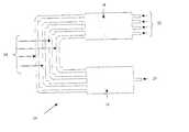
- FIG. 1is a schematic diagram of an exemplary HIC AWG 2 in accordance with the invention.
- the design of the structure and development of the compact HIC AWGcan be fabricated on a high-speed, complementary-bipolar, trench-etched-on-sidewall-oxide-isolated SOI, wafer fabrication process to achieve chip-scale, wavelength-division multiplexing (CS-WDM).
- CS-WDMwavelength-division multiplexing
- the AWG 2includes an input MMI 4 , input arrayed waveguides 10 , an output MMI 6 , and output arrayed waveguides 12 .
- the input MMI 4receives an optical signal from an input waveguide 8 , and proceeds to split the signal into 4 channels in the C-band. In other embodiments, the input MMI 4 can split an optical into more than 4 channels, for example, 32 or 40 channels. Each of the signals has a different wavelength or frequency in the C-band.
- the dimensions of the input MMI 4define the range of optical splitting that can be performed.
- the input MMI 4is formed using HIC optics, which is used for producing optical elements with small die areas.
- the input MMI 4provides its outputs to the 4 distinct input arrayed waveguides 10 .
- the input arrayed waveguides 10are a medium for transmitting the 4 C-band signals to the output MMI 8 .
- the input arrayed waveguides 10are designed to have a specified bend in their orientation so that they can be used without taking much space.
- Each of the input arrayed waveguides 10is spaced apart in wavelengths of a defined amount. In this embodiment, the wavelength spacing is approximately 10 nm.
- the input arrayed waveguides 10can have a linear arrangement. Note that the input arrayed waveguides 10 are formed using HIC optics, however, the input arrayed waveguides 10 can also be formed using high transmission cavity (HTC) optics.
- HTChigh transmission cavity
- the input arrayed waveguides 10provide their respective signals to the output MMI 8 .
- the respective signal received to the output MMIare in different C-bands, as formed by the input MMI 4 .
- the output MMI 8maintains the exact C-bands that was formed by the input MMI 4 .
- the output MMI 8filters the noise that is incorporated by having the C-band signals travel in the input arrayed waveguides, and can be used to further split the various C-band signals into finer optical signals.
- the dimensions of the output MMI 6define the range of optical splitting that can be performed.
- the output MMI 6is formed using HIC optics, which is used for producing optical elements with small die areas.
- the output MMI 6outputs each of its signals to the four output arrayed waveguides 12 .
- the input and output MMIs 4 and 6are both the same device, however, in other embodiments, they can be different.
- the output arrayed waveguides 12provide their respective signals as input to an associated optical element for further processing. Note that the output arrayed waveguides 12 are formed using HIC optics.
- mis the diffraction order
- ⁇is the wavelength of diffracted light
- dis the pitch of the arrayed waveguides
- ⁇is the diffraction angle
- ⁇ Lis the path difference in the arrayed waveguides
- n sis the refractive index of the MMI
- n cis the refractive index in the arrayed waveguides
- fis the focal length of output MMI
- ⁇ 0is center wavelength.
- the unknown parametersare the focal length and the diffractions order. Since there is no restriction on the length of the arrayed waveguide in the equations, the AWG size is essentially limited by the curvature of the arrayed waveguides and the size of the input and output MMIs. Here it is assumed that the input MMI has the same geometry as the output MMI.
- FIG. 2is a schematic diagram of an exemplary high transmission cavity (HTC) AWG 14 in accordance with the invention.
- Standard HTC structuresprovide for right angle bends with at least 98% transmittance.
- the design of the structure and development of the compact HTC AWGcan be fabricated on a high-speed, complementary-bipolar, trench-etched-on-sidewall-oxide-isolated SOI, wafer fabrication process to achieve chip-scale, wavelength-division multiplexing (CS-WDM).
- CS-WDMwavelength-division multiplexing
- the size and functions of the HTC AWGis analyzed using previously described grating equations Eq. 1 and Eq. 2.
- the AWG 14includes an input MMI 16 , input arrayed waveguides 24 , an output MMI 18 , and output arrayed waveguides 22 .
- the input MMI 16receives an optical signal from an input waveguide 20 , and proceeds to split the signal into 4 channels in the C-band. In other embodiments, the input MMI 16 can split an optical into more than 4 channels, for example, 32 or 40 channels. Each of the signals has a different wavelength or frequency in the C-band.
- the dimensions of the input MMI 16define the range of optical splitting that can be performed. Furthermore, the input MMI 16 is formed using HTC optics, which is used for producing compact optical elements.
- the input MMI 16provides its outputs to the 4 distinct input arrayed waveguides 24 .
- the input arrayed waveguides 24are a medium for transmitting the 4 C-band signals to the output MMI 18 .
- the input arrayed waveguides 24are designed to have a 90-degree bend in their orientation so that they can be used without taking much space.
- Each of the input arrayed waveguides 24is spaced apart a defined amount. In this embodiment, the spacing is approximately 10 nm. In another embodiment, the input arrayed waveguides 24 can have a linear arrangement.
- the input arrayed waveguides 24provide their respective signals to the output MMI 18 .
- the respective signal received to the output MMI 18are in different C-bands, as formed by the input MMI 4 .
- the output MMI 18maintains the exact C-bands that was formed by the input MMI 16 .
- the output MMI 18filters the noise that is incorporated by having the C-band signals travel in the input arrayed waveguides, and can be used to further split the various C-band signals into finer optical signals.
- the dimensions of the output MMI 18define the range of optical splitting that can be performed.
- the output MMI 18is formed using HTC optics, which is used for producing compact optical elements.
- the output MMI 18outputs each of its signals to the four output arrayed waveguides 22 .
- the input and output MMIs 16 and 18are both the same device, however, in other embodiments, they can be different.
- the output arrayed waveguides 22provide their respective signals as input to an associated optical element for further processing, and they are formed using HTC optics.
- FIG. 3is a table of the size and channel number of HIC AWGs. It is assumed that the footprint and the performance of two typical HIC AWGs where the channel spacing is 10 nm. The spacing corresponds to 4 channels in the C-band. Since the minimum curvatures of the Si and Si 3 N 4 waveguide bends are 1 and 10 ⁇ m respectively, the bending radii are no longer factors that prevent the device shrinkage. This is a significant advantage over HIC AWGs. The diffraction order, m, should be smaller than 40 because of the C-band width approximately 40 nm.
- the size of the MMIsshould be characterized by the product of the focal length and the number of channels (n ch ) times the channel pitch. Based on the analyses discussed previously, the size of the Si MMIs is estimated to be 35 ⁇ 4 ⁇ m 2 for 4 channels and 116 ⁇ 4 ⁇ m 2 for 40 channels.
- the arrayed waveguide partdepends on L as well as ⁇ L.
- Lis assumed to ⁇ L.
- the longest waveguide in the arrayed waveguide partis the outer waveguide, whose length is L+n ch ⁇ L .
- Siit is approximately 18 ⁇ m for a 4-channel AWG and approximately 500 ⁇ m for a 40-channel AWG.
- Si 3 N 4it is approximately 40 ⁇ m for a 4-channel AWG and approximately 900 ⁇ m for a 40-channel AWG. Therefore, scalability to a 32-channel AWG can be achieved.
- the candidate materials in this inventioncan be Si, Si 3 N 4 , and Si(O)N.
- FIG. 2shows the potential of Si and Si 3 N 4 .
- Silicon oxynitride (Si(O)N)is a general term for alloys of SiO 2 and Si 3 N 4 .
- the refractive indexis controllable in the range between 1.46 and 2.0, which is impossible for the Ge-doped SiO 2 system currently being used in LIC PLCs.
- the indexcan be chosen to be 1.56, and thus the index difference from SiO 2 is 0.1.
- the minimum-bending radius for a silicon oxynitride core with SiO 2 claddingscan be 100 ⁇ m.
- the focal lengthshould be 2000 ⁇ m and the ⁇ L is 30 ⁇ m.
- FIG. 4is a schematic diagram of an exemplary interleaver 30 using AWGs 32 , 34 of the invention used in crosstalk.
- the increase in the diffraction ordershould decrease the focal length, while it should increase the path difference.
- the compact 32-channel HIC AWGsare best achieved in the Si materials system.
- Si 3 N 4 systemsare also applicable for HIC AWGs, although the size is a little larger than that on the Si systems.
- Crosstalk with adjacent waveguideswill be ⁇ 15 dB, which is low enough for digital applications using the inventive AWGs.
- inventive AWGsAs for analog applications, extremely low crosstalk of ⁇ 40 dB is required to obtain wide dynamic range.
- the inventionuses interleaver filters.
- the AWGs shown in FIG. 3are designed according to the task previously described.
- the interleaver 30includes micro-ring resonators 36 to divide a signal group with wavelength spacing of free spectral range into to odd and even output channels with doubled channel spacing.
- Two AWGs 32 , 34are connected to these even and odd channels of the interleaver filters.
- the ring resonator 36 with 4 multiple ringsis used to verify that the filter characteristics fit the desired requirements.
- the interleavercould also be as small as an order of wavelength in size.
- Monolithic integration of the interleaver with two AWGsshould be achieved since these components are on the same materials systems, processed by the same Si IC processing, and the footprints are extremely small.
- Insertion losses in generic AWGsare generally small among various MUX/DEMUX, such as dielectric mirror filters and fiber Bragg gratings because there are no abrupt changes of refractive index in device geometry.
- insertion losscould be more serious in the HIC-AWG systems.
- the causes of insertion lossare classified as return loss at junctions between MMI exits and outgoing waveguides, propagation loss in the waveguides and MMIs, bending loss of waveguides, and fiber-to-waveguide coupling loss.
- the bending loss of waveguidescan be compensated for in the HIC-AWG systems so that the dominant factors of the insertion loss are return loss, propagation loss, and fiber coupling loss.
- Return lossis defined as scattering loss at the junction from MMI exits and waveguides.
- the input MMI to arrayed waveguidesthere are two junctions: the input MMI to arrayed waveguides and the output MMI to outgoing waveguide channels. Since the widths of single-mode waveguides are typically as small 0.5 ⁇ m wide and 0.2 ⁇ m thick and the distance between two channels spacing is 1 ⁇ m, mode matching at these junctions is one of the most important requirements in minimizing the total insertion loss of the HIC AWGs. The strategy for minimizing the return loss if it is severe is to use graded effective index at the junction. This should minimize the reflection at these junctions.
- atomically flat sidewalls aligned to ⁇ 110 ⁇can make the propagation loss negligible because the planes are crystallographic facets.
- Si waveguideshave an advantage, since they are single crystal.
- the AWGs with high transmission cavity (HTC)could suppress the propagation loss via facets, since the HTC structures are mostly surrounded with linear sidewalls that could be facets.
- a temperature change between 0 and 70° C.will lead to a shift in the center wavelength ⁇ o through temperature-induced length and refractive index change in the AWG.
Landscapes
- Physics & Mathematics (AREA)
- General Physics & Mathematics (AREA)
- Optics & Photonics (AREA)
- Engineering & Computer Science (AREA)
- Microelectronics & Electronic Packaging (AREA)
- Optical Integrated Circuits (AREA)
Abstract
Description
- This application claims priority from provisional applications Ser. Nos. 60/343,146 filed Nov. 1, 2001 and 60/343,346 filed Dec. 21, 2001.[0001]
- The invention relates to the field of array waveguide grating, and in particular a high-index-contrast array waveguide grating photonic integrated circuit.[0002]
- Rapid growth of high-speed, broadband communication has led to a need to increase the capacity of optical communication networks. Wavelength division multiplexing (WDM) systems have key roles in meeting this need. Such networks require a variety of optical components to enable them to directly process light signals. Planar lightwave circuits (PLCs) fabricated using SiO[0003]2-based waveguides are employed in various devices. Of the various types of PLCs, arrayed waveguide gratings (AWGs) are superior to other types of wavelength multiplexers/demultiplexers (MUX/DEMUX), such as dielectric multiplayer filters and fiber Bragg gratings in terms of compactness and large channel number. Thus, 16 to 64 channel AWGs have already been marketed and are widely used as MUX/DEMUX in WDM systems employed in communication networks.
- Despite the advantages of AWGs, there are three other fundamental limits on today's AWGs. The first limit is the large footprint. PLCs employ SiO[0004]2materials technologies developed for optical fibers, whose index contrast is less than 1%, referred to as a low-index contrast (LIC) system. The index contrast is defined as (ncore−ncladding)/ncor. While the LIC platform provides a low-loss technology, it necessitates large waveguide bends, typically approximately 1 cm, due to the weak confinement of light. Current AWGs require footprints of about 10×10 cm2.
- The second limit is hybrid integration with other optical devices. In order to achieve WDM systems, there is a need to use various devices, such as interleavers, photodetectors, and electronic circuitry. Current integration methods are necessarily hybrid due to the large footprints and thick structures, leading to low production yields and high cost.[0005]
- The third limit is its thermal instability. Since the bending radii in LIC AWGs are large, the arrayed waveguides are extremely long, typically leading to shifts in the center channel wavelengths. Current SiO[0006]2-based AWGs show length changes of 0.011 nm/° C. Thus, thermal controller footprints similar to those of the AWGs are necessary to keep the AWG performances constant.
- According to one aspect of the invention, there is provided an array waveguide grating structure. The array waveguide grating structure includes an input multi-mode interferometer (MMI) that receives an input optical signal and splits the optical signal into a plurality of signals, each having a defined wavelength. A plurality of input arrayed waveguide structures receives the plurality of signals such that each of the waveguide structures receives one of the plurality of signals. The input MMI, the plurality of arrayed waveguide structures, and the output waveguide are configured using high index contrast (HIC) or high transmission cavity (HTC) optics.[0007]
- According to another aspect of the invention, there is provided a method of forming an array waveguide grating structure. The method includes providing an input MMI that receives an input optical signal and splits the optical signal into a plurality of signals, each having a defined wavelength. The method also includes providing a plurality of input arrayed waveguide structures receiving the plurality of signals such that each of the waveguide structures receives one of the plurality of signals. Furthermore, the method includes providing an output MMI receiving the plurality of signals from the plurality input of arrayed structures so that the plurality of signals are maintained in accordance with each of the wavelength as defined for the plurality of signals by the input MMI. The input MMI, the plurality of arrayed waveguide structures, and the output waveguide are configured using HIC or HTC optics.[0008]
- FIG. 1 is a schematic diagram of a HIC AWG;[0009]
- FIG. 2 is schematic diagram of a HTC AWG.[0010]
- FIG. 3 is a table of the size and channel number of HIC AWGs; and[0011]
- FIG. 4 is a schematic diagram of an exemplary interleaver in accordance with the invention.[0012]
- High index contrast (HIC) structures are a new platform from which to make optical components within a small die area. Typical high index materials include Si and Si[0013]3N4, with indices 3.5 and approximately 2.2, respectively. The index contrasts with SiO2cladding layers are approximately 60 and 40%, respectively.
- The HIC system strongly confines light in the cores, allowing sharp bends, and therefore, small footprints. Having small footprints also enhance the thermal stability because of the negligible expansion of the waveguides. Si and Si[0014]3N4materials are Si IC process compatible. However, sidewall roughness is a crucial factor for low-loss waveguides. Based on the theory to predict the effects of sidewall roughness on light scattering, Si is more sensitive to roughness than is Si3N4or Si(O)N. However, Si has facet planes, which are atomically flat and can be controlled by post-process annealing. In this way, the sidewall roughness can be controllable.
- For analog signal processing, the crosstalk between adjacent channels should be as small as approximately 40 dB. Interleaver filters can be used to achieve such a low crosstalk. Generic interleavers in SiO[0015]2-based PLCs will consist of a set of 3 dB directional couplers/splitters to divide a signal group with a wavelength spacing of Δλ into two (odd and even) channels with a wavelength spacing of 2Δλ, thereby reducing the adjacent channel crosstalk. Use of the AWGs in digital applications does not require such a low crosstalk.
- Thermal stability depends on the temperature dependence of the refractive index, in addition to the linear expansion coefficient of the waveguide materials. Silicon's index has a larger temperature dependence than does Si[0016]3N4's index.
- FIG. 1 is a schematic diagram of an exemplary HIC AWG[0017]2 in accordance with the invention. The design of the structure and development of the compact HIC AWG can be fabricated on a high-speed, complementary-bipolar, trench-etched-on-sidewall-oxide-isolated SOI, wafer fabrication process to achieve chip-scale, wavelength-division multiplexing (CS-WDM). The size and functions of the HIC AWG is analyzed using grating equations.
- The AWG[0018]2 includes an
input MMI 4, input arrayedwaveguides 10, anoutput MMI 6, and output arrayedwaveguides 12. Theinput MMI 4 receives an optical signal from aninput waveguide 8, and proceeds to split the signal into 4 channels in the C-band. In other embodiments, theinput MMI 4 can split an optical into more than 4 channels, for example, 32 or 40 channels. Each of the signals has a different wavelength or frequency in the C-band. The dimensions of theinput MMI 4 define the range of optical splitting that can be performed. Furthermore, theinput MMI 4 is formed using HIC optics, which is used for producing optical elements with small die areas. - The[0019]
input MMI 4 provides its outputs to the 4 distinct input arrayedwaveguides 10. The input arrayedwaveguides 10 are a medium for transmitting the 4 C-band signals to theoutput MMI 8. Also, the input arrayedwaveguides 10 are designed to have a specified bend in their orientation so that they can be used without taking much space. Each of the input arrayedwaveguides 10 is spaced apart in wavelengths of a defined amount. In this embodiment, the wavelength spacing is approximately 10 nm. In another embodiment, the input arrayedwaveguides 10 can have a linear arrangement. Note that the input arrayedwaveguides 10 are formed using HIC optics, however, the input arrayedwaveguides 10 can also be formed using high transmission cavity (HTC) optics. - The input arrayed[0020]
waveguides 10 provide their respective signals to theoutput MMI 8. The respective signal received to the output MMI are in different C-bands, as formed by theinput MMI 4. Theoutput MMI 8 maintains the exact C-bands that was formed by theinput MMI 4. In particular, theoutput MMI 8 filters the noise that is incorporated by having the C-band signals travel in the input arrayed waveguides, and can be used to further split the various C-band signals into finer optical signals. - As discussed previously regarding the[0021]
input MMI 4, the dimensions of theoutput MMI 6 define the range of optical splitting that can be performed. However, theoutput MMI 6 is formed using HIC optics, which is used for producing optical elements with small die areas. Furthermore, theoutput MMI 6 outputs each of its signals to the four output arrayedwaveguides 12. In this embodiment, the input and output MMIs4 and6 are both the same device, however, in other embodiments, they can be different. - The output arrayed[0022]
waveguides 12 provide their respective signals as input to an associated optical element for further processing. Note that the output arrayedwaveguides 12 are formed using HIC optics. - Theoretical analyses have been made to predict the size and functionality of generic AWG structures on the HIC platform shown in FIG. 1. Four channels are assumed for the WDM integration, but the scalability to 32 channels is examined. Both digital and analog applications in the C-band are considered. Interleaver filters are necessary for analog applications, where crosstalk with the adjacent waveguide of −40 dB is assumed. The thermal stability of the performance is checked between 0 to 70° C. The analyses have demonstrated that the AWGS with typical size approximately 100×100 μm[0023]2should be achievable using high-index contrast optics based on Si or Si3N4core layers with SiO2cladding layers.
- The following set of grating equations are used to evaluate the fundamental size minimization limits:[0024]
- m·λ=ns·d·sinθ+nc·ΔL Eq. 1
- where m is the diffraction order, λ is the wavelength of diffracted light, d is the pitch of the arrayed waveguides, θ is the diffraction angle, ΔL is the path difference in the arrayed waveguides, n[0026]sis the refractive index of the MMI, ncis the refractive index in the arrayed waveguides, f is the focal length of output MMI, and λ0is center wavelength.
- The unknown parameters are the focal length and the diffractions order. Since there is no restriction on the length of the arrayed waveguide in the equations, the AWG size is essentially limited by the curvature of the arrayed waveguides and the size of the input and output MMIs. Here it is assumed that the input MMI has the same geometry as the output MMI.[0027]
- FIG. 2 is a schematic diagram of an exemplary high transmission cavity (HTC)[0028]
AWG 14 in accordance with the invention. Standard HTC structures provide for right angle bends with at least 98% transmittance. The design of the structure and development of the compact HTC AWG can be fabricated on a high-speed, complementary-bipolar, trench-etched-on-sidewall-oxide-isolated SOI, wafer fabrication process to achieve chip-scale, wavelength-division multiplexing (CS-WDM). The size and functions of the HTC AWG is analyzed using previously described grating equations Eq. 1 and Eq. 2. - The[0029]
AWG 14 includes aninput MMI 16, input arrayedwaveguides 24, anoutput MMI 18, and output arrayedwaveguides 22. Theinput MMI 16 receives an optical signal from aninput waveguide 20, and proceeds to split the signal into 4 channels in the C-band. In other embodiments, theinput MMI 16 can split an optical into more than 4 channels, for example, 32 or 40 channels. Each of the signals has a different wavelength or frequency in the C-band. The dimensions of theinput MMI 16 define the range of optical splitting that can be performed. Furthermore, theinput MMI 16 is formed using HTC optics, which is used for producing compact optical elements. - The[0030]
input MMI 16 provides its outputs to the 4 distinct input arrayedwaveguides 24. The input arrayedwaveguides 24 are a medium for transmitting the 4 C-band signals to theoutput MMI 18. Also, the input arrayedwaveguides 24 are designed to have a 90-degree bend in their orientation so that they can be used without taking much space. Each of the input arrayedwaveguides 24 is spaced apart a defined amount. In this embodiment, the spacing is approximately 10 nm. In another embodiment, the input arrayedwaveguides 24 can have a linear arrangement. - The input arrayed[0031]
waveguides 24 provide their respective signals to theoutput MMI 18. The respective signal received to theoutput MMI 18 are in different C-bands, as formed by theinput MMI 4. Theoutput MMI 18 maintains the exact C-bands that was formed by theinput MMI 16. In particular, theoutput MMI 18 filters the noise that is incorporated by having the C-band signals travel in the input arrayed waveguides, and can be used to further split the various C-band signals into finer optical signals. - As discussed previously regarding the[0032]
input MMI 16, the dimensions of theoutput MMI 18 define the range of optical splitting that can be performed. However, theoutput MMI 18 is formed using HTC optics, which is used for producing compact optical elements. Furthermore, theoutput MMI 18 outputs each of its signals to the four output arrayedwaveguides 22. In this embodiment, the input and output MMIs16 and18 are both the same device, however, in other embodiments, they can be different. - The output arrayed[0033]
waveguides 22 provide their respective signals as input to an associated optical element for further processing, and they are formed using HTC optics. - FIG. 3 is a table of the size and channel number of HIC AWGs. It is assumed that the footprint and the performance of two typical HIC AWGs where the channel spacing is 10 nm. The spacing corresponds to 4 channels in the C-band. Since the minimum curvatures of the Si and Si[0034]3N4waveguide bends are 1 and 10 μm respectively, the bending radii are no longer factors that prevent the device shrinkage. This is a significant advantage over HIC AWGs. The diffraction order, m, should be smaller than 40 because of the C-band width approximately 40 nm.
- The dimensions for the 10 nm spacing are summarized in FIG. 2. For Si, the diffraction angle is 1.6°, focal length f is 3.5 μm , and ΔL is 7.7 μm when m is 10. It is clear that the footprints of the 4-channel HIC AWG are less than 100×100 μm[0035]2. The parameters for the case of a 1 nm channel spacing, for example 40-channel AWGs, are also summarized in FIG. 2. Here, the focal length is a decisive parameter for the shrinkage.
- The size of the MMIs should be characterized by the product of the focal length and the number of channels (n[0036]ch) times the channel pitch. Based on the analyses discussed previously, the size of the Si MMIs is estimated to be 35×4 μm2for 4 channels and 116×4 μm2for 40 channels.
- The arrayed waveguide part depends on L as well as ΔL. Here it is assumed L is equal to ΔL. Then the longest waveguide in the arrayed waveguide part is the outer waveguide, whose length is L+n[0037]chΔL . In other words, in Si it is approximately 18 μm for a 4-channel AWG and approximately 500 μm for a 40-channel AWG. In Si3N4, it is approximately 40 μm for a 4-channel AWG and approximately 900 μm for a 40-channel AWG. Therefore, scalability to a 32-channel AWG can be achieved.
- The candidate materials in this invention can be Si, Si[0038]3N4, and Si(O)N. FIG. 2 shows the potential of Si and Si3N4. Silicon oxynitride (Si(O)N) is a general term for alloys of SiO2and Si3N4. The refractive index is controllable in the range between 1.46 and 2.0, which is impossible for the Ge-doped SiO2system currently being used in LIC PLCs. The index can be chosen to be 1.56, and thus the index difference from SiO2is 0.1.
- The minimum-bending radius for a silicon oxynitride core with SiO[0039]2claddings can be 100 μm. When the channel spacing is 10 nm, the focal length should be 2000 μm and the ΔL is 30 μm.
- FIG. 4 is a schematic diagram of an[0040]
exemplary interleaver 30 usingAWGs - Crosstalk with adjacent waveguides will be −15 dB, which is low enough for digital applications using the inventive AWGs. As for analog applications, extremely low crosstalk of −40 dB is required to obtain wide dynamic range. In order to realize such a low crosstalk, the invention uses interleaver filters. The AWGs shown in FIG. 3 are designed according to the task previously described.[0041]
- The[0042]
interleaver 30 includesmicro-ring resonators 36 to divide a signal group with wavelength spacing of free spectral range into to odd and even output channels with doubled channel spacing. TwoAWGs ring resonator 36 with 4 multiple rings is used to verify that the filter characteristics fit the desired requirements. As the bending radius is not a decisive factor, the interleaver could also be as small as an order of wavelength in size. Monolithic integration of the interleaver with two AWGs should be achieved since these components are on the same materials systems, processed by the same Si IC processing, and the footprints are extremely small. - Insertion losses in generic AWGs are generally small among various MUX/DEMUX, such as dielectric mirror filters and fiber Bragg gratings because there are no abrupt changes of refractive index in device geometry. However, insertion loss could be more serious in the HIC-AWG systems. The causes of insertion loss are classified as return loss at junctions between MMI exits and outgoing waveguides, propagation loss in the waveguides and MMIs, bending loss of waveguides, and fiber-to-waveguide coupling loss. The bending loss of waveguides can be compensated for in the HIC-AWG systems so that the dominant factors of the insertion loss are return loss, propagation loss, and fiber coupling loss.[0043]
- Return loss is defined as scattering loss at the junction from MMI exits and waveguides. In other words, there are two junctions: the input MMI to arrayed waveguides and the output MMI to outgoing waveguide channels. Since the widths of single-mode waveguides are typically as small 0.5 μm wide and 0.2 μm thick and the distance between two channels spacing is 1 μm, mode matching at these junctions is one of the most important requirements in minimizing the total insertion loss of the HIC AWGs. The strategy for minimizing the return loss if it is severe is to use graded effective index at the junction. This should minimize the reflection at these junctions.[0044]
- Light scattering in terms of the waveguide surface roughness induces the propagation loss in the waveguides and MMIs. The top and bottom interfaces of the waveguide core with the cladding is essentially smooth since these interfaces are obtained by deposition or as SOI structures. However, the sidewalls are fabricated by lithography and etching processing, so the roughness is strongly dependent on the evolution of lithographic and etch technology. It is predicted that the propagation loss depends on the amplitude and the periodicity of the roughness. There is a loss peak in the roughness period. This period corresponds to a quarter-lambda wavelength in the waveguides.[0045]
- By minimizing surface roughness, it could reduce the propagation loss. For example, atomically flat sidewalls aligned to {110} can make the propagation loss negligible because the planes are crystallographic facets. Si waveguides have an advantage, since they are single crystal. The AWGs with high transmission cavity (HTC) could suppress the propagation loss via facets, since the HTC structures are mostly surrounded with linear sidewalls that could be facets.[0046]
- The temperature dependence of the linear expansion coefficient of Si ΔL/L is reported to be 2.6×10[0048]−6° C.−1and the relative index n is 3.38×(1+3.9×10⁻⁵T). On the other hand, the temperature dependences for Si3N4are 2.8×10⁻⁶° C.−1and the relative index n is 2.0×(1+2×10⁻⁶T), respectively. The shift of the center wavelength is calculated to be 0.004 nm/° C. Although strain induced by the temperature fluctuation is not taken into account, there is no need for thermal stabilization of 4-channel AWGs. To scale to 32 channels, Si3N4based on AWGs should be advantageous over Si but both should work with a moderate thermal controller.
- Although the present invention has been shown and described with respect to several preferred embodiments thereof, various changes, omissions and additions to the form and detail thereof, may be made therein, without departing from the spirit and scope of the invention.[0049]


Claims (24)
Priority Applications (1)
| Application Number | Priority Date | Filing Date | Title |
|---|---|---|---|
| US10/285,865US7043120B2 (en) | 2001-11-01 | 2002-11-01 | Array waveguide grating |
Applications Claiming Priority (3)
| Application Number | Priority Date | Filing Date | Title |
|---|---|---|---|
| US33114601P | 2001-11-01 | 2001-11-01 | |
| US34334601P | 2001-12-21 | 2001-12-21 | |
| US10/285,865US7043120B2 (en) | 2001-11-01 | 2002-11-01 | Array waveguide grating |
Publications (2)
| Publication Number | Publication Date |
|---|---|
| US20030128927A1true US20030128927A1 (en) | 2003-07-10 |
| US7043120B2 US7043120B2 (en) | 2006-05-09 |
Family
ID=26987610
Family Applications (1)
| Application Number | Title | Priority Date | Filing Date |
|---|---|---|---|
| US10/285,865Expired - LifetimeUS7043120B2 (en) | 2001-11-01 | 2002-11-01 | Array waveguide grating |
Country Status (3)
| Country | Link |
|---|---|
| US (1) | US7043120B2 (en) |
| AU (1) | AU2002353969A1 (en) |
| WO (1) | WO2003038501A2 (en) |
Cited By (2)
| Publication number | Priority date | Publication date | Assignee | Title |
|---|---|---|---|---|
| US20030142942A1 (en)* | 2001-11-14 | 2003-07-31 | Hitachi Cable, Ltd. | Silica based glass waveguide and optical module using the same |
| US20070025670A1 (en)* | 2005-08-01 | 2007-02-01 | Dong Pan | Method of fabricating Ge or SiGe/Si waveguide or photonic crystal structures by selective growth |
Families Citing this family (10)
| Publication number | Priority date | Publication date | Assignee | Title |
|---|---|---|---|---|
| TWM276207U (en)* | 2004-10-01 | 2005-09-21 | Hung-Jr Lu | Array waveguide grating device |
| US7397986B2 (en)* | 2005-03-04 | 2008-07-08 | Gemfire Corporation | Optical device with reduced temperature dependence |
| EP2548058B1 (en)* | 2010-03-19 | 2014-11-19 | Gemfire Corporation | Arrayed waveguide grating compensated in temperature up to the second order with longitudinal slots therein |
| US8649645B2 (en) | 2011-06-10 | 2014-02-11 | Xyratex Technology Limited | Optical waveguide and a method of fabricating an optical waveguide |
| US9616641B2 (en) | 2011-06-24 | 2017-04-11 | Corning Incorporated | Light-weight hybrid glass laminates |
| US10571631B2 (en) | 2015-01-05 | 2020-02-25 | The Research Foundation For The State University Of New York | Integrated photonics including waveguiding material |
| US10976491B2 (en) | 2016-11-23 | 2021-04-13 | The Research Foundation For The State University Of New York | Photonics interposer optoelectronics |
| US10698156B2 (en) | 2017-04-27 | 2020-06-30 | The Research Foundation For The State University Of New York | Wafer scale bonded active photonics interposer |
| WO2019195441A1 (en) | 2018-04-04 | 2019-10-10 | The Research Foundation For The State University Of New York | Heterogeneous structure on an integrated photonics platform |
| US10816724B2 (en) | 2018-04-05 | 2020-10-27 | The Research Foundation For The State University Of New York | Fabricating photonics structure light signal transmission regions |
Citations (21)
| Publication number | Priority date | Publication date | Assignee | Title |
|---|---|---|---|---|
| US5862279A (en)* | 1994-02-11 | 1999-01-19 | U.S. Philips Corporation | Optical device with phased array |
| US6069990A (en)* | 1997-11-27 | 2000-05-30 | Hitachi Cable Ltd. | Optical wavelength multiplexer/demultiplexer |
| US6289147B1 (en)* | 1999-11-01 | 2001-09-11 | Bbv Design Bv | Passband flattening of a phasar |
| US6421481B1 (en)* | 2000-02-04 | 2002-07-16 | Zolo Technologies, Inc. | Apparatus and method for producing a flat-topped filter response for diffraction grating (De) multiplexer |
| US20020141704A1 (en)* | 2000-11-28 | 2002-10-03 | Lim Desmond R. | Three dimensional high index optical waveguides bends and splitters |
| US20020164118A1 (en)* | 2001-04-05 | 2002-11-07 | Paddon Paul J. | Photonic input/output port |
| US6512864B1 (en)* | 2000-06-08 | 2003-01-28 | Lucent Technologies Inc. | Optical multiplexer/demultiplexer arrangement for WDM signals having in-band and out-of-band signal components |
| US6529649B1 (en)* | 2000-05-01 | 2003-03-04 | Lucent Technologies Inc. | Optical filter with improved crosstalk rejection |
| US6539150B2 (en)* | 2000-12-13 | 2003-03-25 | Alcatel Optronics Uk Limited | Segmented waveguide flattening the passband of a phasar |
| US6549696B1 (en)* | 1999-08-10 | 2003-04-15 | Hitachi Cable, Ltd. | Optical wavelength multiplexer/demultiplexer |
| US6571038B1 (en)* | 2000-03-01 | 2003-05-27 | Lucent Technologies Inc. | Multimode interference coupler with tunable power splitting ratios and method of tuning |
| US20030099425A1 (en)* | 2001-11-06 | 2003-05-29 | Grubb Stephen G. | Optical communication module with one or more photonic integrated circuit (PIC) chips and an external booster optical amplifier for photonic integrated circuits (PICs) |
| US6587615B1 (en)* | 1999-05-11 | 2003-07-01 | Jds Fitel Inc. | Wavelength multiplexer-demultiplexer having a wide flat response within the spectral passband |
| US6643419B2 (en)* | 2001-12-05 | 2003-11-04 | Pacific Wave Industries, Inc. | Ultra-high speed, active polymer-silica hybrid, single control voltage MMI-based 1-by-N packet switch and WG-based WDM packet router/TDM converter and methods of making same |
| US6701090B1 (en)* | 1999-07-28 | 2004-03-02 | Sumitomo Electric Industries, Ltd. | Wavelength division multiplexing signal number monitoring apparatus and method |
| US20040076394A1 (en)* | 2000-10-27 | 2004-04-22 | Federico Carniel | Hybrid buried/ridge planar waveguides |
| US6768842B2 (en)* | 2001-09-11 | 2004-07-27 | Alcatel Optronics Uk Limited | Arrayed waveguide grating |
| US6807349B2 (en)* | 2001-09-04 | 2004-10-19 | Michael Bazylenko | Planer waveguide and method of formation |
| US6839491B2 (en)* | 2000-12-21 | 2005-01-04 | Xponent Photonics Inc | Multi-layer dispersion-engineered waveguides and resonators |
| US6856733B2 (en)* | 2001-12-07 | 2005-02-15 | Intel Corporation | 1xN fanout waveguide photodetector |
| US6888985B2 (en)* | 2000-06-29 | 2005-05-03 | Nec Corporation | Arrayed waveguide grating and optical communication system using arrayed waveguide grating |
- 2002
- 2002-11-01AUAU2002353969Apatent/AU2002353969A1/ennot_activeAbandoned
- 2002-11-01WOPCT/US2002/035125patent/WO2003038501A2/ennot_activeApplication Discontinuation
- 2002-11-01USUS10/285,865patent/US7043120B2/ennot_activeExpired - Lifetime
Patent Citations (21)
| Publication number | Priority date | Publication date | Assignee | Title |
|---|---|---|---|---|
| US5862279A (en)* | 1994-02-11 | 1999-01-19 | U.S. Philips Corporation | Optical device with phased array |
| US6069990A (en)* | 1997-11-27 | 2000-05-30 | Hitachi Cable Ltd. | Optical wavelength multiplexer/demultiplexer |
| US6587615B1 (en)* | 1999-05-11 | 2003-07-01 | Jds Fitel Inc. | Wavelength multiplexer-demultiplexer having a wide flat response within the spectral passband |
| US6701090B1 (en)* | 1999-07-28 | 2004-03-02 | Sumitomo Electric Industries, Ltd. | Wavelength division multiplexing signal number monitoring apparatus and method |
| US6549696B1 (en)* | 1999-08-10 | 2003-04-15 | Hitachi Cable, Ltd. | Optical wavelength multiplexer/demultiplexer |
| US6289147B1 (en)* | 1999-11-01 | 2001-09-11 | Bbv Design Bv | Passband flattening of a phasar |
| US6421481B1 (en)* | 2000-02-04 | 2002-07-16 | Zolo Technologies, Inc. | Apparatus and method for producing a flat-topped filter response for diffraction grating (De) multiplexer |
| US6571038B1 (en)* | 2000-03-01 | 2003-05-27 | Lucent Technologies Inc. | Multimode interference coupler with tunable power splitting ratios and method of tuning |
| US6529649B1 (en)* | 2000-05-01 | 2003-03-04 | Lucent Technologies Inc. | Optical filter with improved crosstalk rejection |
| US6512864B1 (en)* | 2000-06-08 | 2003-01-28 | Lucent Technologies Inc. | Optical multiplexer/demultiplexer arrangement for WDM signals having in-band and out-of-band signal components |
| US6888985B2 (en)* | 2000-06-29 | 2005-05-03 | Nec Corporation | Arrayed waveguide grating and optical communication system using arrayed waveguide grating |
| US20040076394A1 (en)* | 2000-10-27 | 2004-04-22 | Federico Carniel | Hybrid buried/ridge planar waveguides |
| US20020141704A1 (en)* | 2000-11-28 | 2002-10-03 | Lim Desmond R. | Three dimensional high index optical waveguides bends and splitters |
| US6539150B2 (en)* | 2000-12-13 | 2003-03-25 | Alcatel Optronics Uk Limited | Segmented waveguide flattening the passband of a phasar |
| US6839491B2 (en)* | 2000-12-21 | 2005-01-04 | Xponent Photonics Inc | Multi-layer dispersion-engineered waveguides and resonators |
| US20020164118A1 (en)* | 2001-04-05 | 2002-11-07 | Paddon Paul J. | Photonic input/output port |
| US6807349B2 (en)* | 2001-09-04 | 2004-10-19 | Michael Bazylenko | Planer waveguide and method of formation |
| US6768842B2 (en)* | 2001-09-11 | 2004-07-27 | Alcatel Optronics Uk Limited | Arrayed waveguide grating |
| US20030099425A1 (en)* | 2001-11-06 | 2003-05-29 | Grubb Stephen G. | Optical communication module with one or more photonic integrated circuit (PIC) chips and an external booster optical amplifier for photonic integrated circuits (PICs) |
| US6643419B2 (en)* | 2001-12-05 | 2003-11-04 | Pacific Wave Industries, Inc. | Ultra-high speed, active polymer-silica hybrid, single control voltage MMI-based 1-by-N packet switch and WG-based WDM packet router/TDM converter and methods of making same |
| US6856733B2 (en)* | 2001-12-07 | 2005-02-15 | Intel Corporation | 1xN fanout waveguide photodetector |
Cited By (4)
| Publication number | Priority date | Publication date | Assignee | Title |
|---|---|---|---|---|
| US20030142942A1 (en)* | 2001-11-14 | 2003-07-31 | Hitachi Cable, Ltd. | Silica based glass waveguide and optical module using the same |
| US7415183B2 (en)* | 2001-11-14 | 2008-08-19 | Hitachi Cable, Ltd. | Silica based glass waveguide and optical module using the same |
| US20070025670A1 (en)* | 2005-08-01 | 2007-02-01 | Dong Pan | Method of fabricating Ge or SiGe/Si waveguide or photonic crystal structures by selective growth |
| US7801406B2 (en)* | 2005-08-01 | 2010-09-21 | Massachusetts Institute Of Technology | Method of fabricating Ge or SiGe/Si waveguide or photonic crystal structures by selective growth |
Also Published As
| Publication number | Publication date |
|---|---|
| WO2003038501A2 (en) | 2003-05-08 |
| US7043120B2 (en) | 2006-05-09 |
| AU2002353969A1 (en) | 2003-05-12 |
| WO2003038501A3 (en) | 2003-10-16 |
Similar Documents
| Publication | Publication Date | Title |
|---|---|---|
| US4740951A (en) | Reversible device for the demultiplexing of several light signals in integrated optics | |
| US6757454B2 (en) | Polarization desensitized optical waveguide interferometer | |
| US5341444A (en) | Polarization compensated integrated optical filters and multiplexers | |
| Okamoto | Wavelength-division-multiplexing devices in thin SOI: Advances and prospects | |
| US6181848B1 (en) | Temperature-independent optical multiplexer and/or demultiplexer | |
| JP3794327B2 (en) | Optical coupler and manufacturing method thereof | |
| US6931180B2 (en) | Method and apparatus for compactly coupling an optical fiber and a planar optical waveguide | |
| JP2005010805A6 (en) | Waveguide type optical interferometer | |
| US6256442B1 (en) | Athermal integrated optical waveguide device | |
| US7043120B2 (en) | Array waveguide grating | |
| EP1059545B1 (en) | Arrayed waveguide grating multiplexer and demultiplexer | |
| US11860411B2 (en) | Super-compact arrayed waveguide grating (AWG) wavelength division multiplexer based on sub-wavelength grating | |
| US20020154861A1 (en) | Arrayed waveguide grating optical multiplexer/demultiplexer | |
| Cheben et al. | Scaling down photonic waveguide devices on the SOI platform | |
| US7006729B2 (en) | Optical components having reduced insertion loss | |
| US6798952B2 (en) | Optical multiplexer/demultiplexer | |
| EP1130424B1 (en) | Optical waveguide circuit | |
| US20040151459A1 (en) | Method of polarisation compensation in grating- and phasar-based devices by using over-layer deposited on the compensating region to modify local slab waveguide birefringence | |
| EP1640754A1 (en) | Optical interferometer device description | |
| Dai et al. | Elimination of multimode effects in a silicon-on-insulator etched diffraction grating demultiplexer with bi-level taper structure | |
| Janz et al. | Planar waveguide echelle gratings: an embeddable diffractive element for photonic integrated circuits | |
| JP2005301301A (en) | Optical coupler | |
| EP0982607A1 (en) | Athermal integrated optical waveguide device | |
| Dai et al. | Compact silicon-based wavelength-selective photonic integrated devices and the applications | |
| US6522811B1 (en) | Arrayed waveguide grating |
Legal Events
| Date | Code | Title | Description |
|---|---|---|---|
| AS | Assignment | Owner name:CENTRAL INDUSTRIAL SUPPLY COMPANY, TEXAS Free format text:ASSIGNMENT OF ASSIGNORS INTEREST;ASSIGNORS:BAIZA, JULIAN S.;ALAMILLO, JESUS A.;REEL/FRAME:013454/0432 Effective date:20021028 | |
| AS | Assignment | Owner name:MASSACHUSETTS INSTITUTE OF TECHNOLOGY, MASSACHUSET Free format text:ASSIGNMENT OF ASSIGNORS INTEREST;ASSIGNORS:WADA, KAZUMI;HAUS, HERMANN A.;KIMERLING, LIONEL C.;REEL/FRAME:013822/0499;SIGNING DATES FROM 20030213 TO 20030214 | |
| STCF | Information on status: patent grant | Free format text:PATENTED CASE | |
| FEPP | Fee payment procedure | Free format text:PAT HOLDER NO LONGER CLAIMS SMALL ENTITY STATUS, ENTITY STATUS SET TO UNDISCOUNTED (ORIGINAL EVENT CODE: STOL); ENTITY STATUS OF PATENT OWNER: LARGE ENTITY | |
| FPAY | Fee payment | Year of fee payment:4 | |
| FEPP | Fee payment procedure | Free format text:PAYER NUMBER DE-ASSIGNED (ORIGINAL EVENT CODE: RMPN); ENTITY STATUS OF PATENT OWNER: LARGE ENTITY Free format text:PAYOR NUMBER ASSIGNED (ORIGINAL EVENT CODE: ASPN); ENTITY STATUS OF PATENT OWNER: LARGE ENTITY | |
| FPAY | Fee payment | Year of fee payment:8 | |
| MAFP | Maintenance fee payment | Free format text:PAYMENT OF MAINTENANCE FEE, 12TH YEAR, LARGE ENTITY (ORIGINAL EVENT CODE: M1553) Year of fee payment:12 |