US20030128612A1 - PCRAM rewrite prevention - Google Patents
PCRAM rewrite preventionDownload PDFInfo
- Publication number
- US20030128612A1 US20030128612A1US10/035,197US3519702AUS2003128612A1US 20030128612 A1US20030128612 A1US 20030128612A1US 3519702 AUS3519702 AUS 3519702AUS 2003128612 A1US2003128612 A1US 2003128612A1
- Authority
- US
- United States
- Prior art keywords
- bit line
- sense amplifier
- memory cell
- activated
- addressed
- Prior art date
- Legal status (The legal status is an assumption and is not a legal conclusion. Google has not performed a legal analysis and makes no representation as to the accuracy of the status listed.)
- Granted
Links
Images


Classifications
- G—PHYSICS
- G11—INFORMATION STORAGE
- G11C—STATIC STORES
- G11C7/00—Arrangements for writing information into, or reading information out from, a digital store
- G—PHYSICS
- G11—INFORMATION STORAGE
- G11C—STATIC STORES
- G11C13/00—Digital stores characterised by the use of storage elements not covered by groups G11C11/00, G11C23/00, or G11C25/00
- G11C13/0002—Digital stores characterised by the use of storage elements not covered by groups G11C11/00, G11C23/00, or G11C25/00 using resistive RAM [RRAM] elements
- G11C13/0004—Digital stores characterised by the use of storage elements not covered by groups G11C11/00, G11C23/00, or G11C25/00 using resistive RAM [RRAM] elements comprising amorphous/crystalline phase transition cells
- G—PHYSICS
- G11—INFORMATION STORAGE
- G11C—STATIC STORES
- G11C11/00—Digital stores characterised by the use of particular electric or magnetic storage elements; Storage elements therefor
- G11C11/21—Digital stores characterised by the use of particular electric or magnetic storage elements; Storage elements therefor using electric elements
- G11C11/34—Digital stores characterised by the use of particular electric or magnetic storage elements; Storage elements therefor using electric elements using semiconductor devices
- G11C11/40—Digital stores characterised by the use of particular electric or magnetic storage elements; Storage elements therefor using electric elements using semiconductor devices using transistors
- G11C11/401—Digital stores characterised by the use of particular electric or magnetic storage elements; Storage elements therefor using electric elements using semiconductor devices using transistors forming cells needing refreshing or charge regeneration, i.e. dynamic cells
- G11C11/406—Management or control of the refreshing or charge-regeneration cycles
- G—PHYSICS
- G11—INFORMATION STORAGE
- G11C—STATIC STORES
- G11C11/00—Digital stores characterised by the use of particular electric or magnetic storage elements; Storage elements therefor
- G11C11/21—Digital stores characterised by the use of particular electric or magnetic storage elements; Storage elements therefor using electric elements
- G11C11/34—Digital stores characterised by the use of particular electric or magnetic storage elements; Storage elements therefor using electric elements using semiconductor devices
- G11C11/40—Digital stores characterised by the use of particular electric or magnetic storage elements; Storage elements therefor using electric elements using semiconductor devices using transistors
- G11C11/401—Digital stores characterised by the use of particular electric or magnetic storage elements; Storage elements therefor using electric elements using semiconductor devices using transistors forming cells needing refreshing or charge regeneration, i.e. dynamic cells
- G11C11/4063—Auxiliary circuits, e.g. for addressing, decoding, driving, writing, sensing or timing
- G11C11/407—Auxiliary circuits, e.g. for addressing, decoding, driving, writing, sensing or timing for memory cells of the field-effect type
- G11C11/409—Read-write [R-W] circuits
- G11C11/4091—Sense or sense/refresh amplifiers, or associated sense circuitry, e.g. for coupled bit-line precharging, equalising or isolating
- G—PHYSICS
- G11—INFORMATION STORAGE
- G11C—STATIC STORES
- G11C13/00—Digital stores characterised by the use of storage elements not covered by groups G11C11/00, G11C23/00, or G11C25/00
- G11C13/0002—Digital stores characterised by the use of storage elements not covered by groups G11C11/00, G11C23/00, or G11C25/00 using resistive RAM [RRAM] elements
- G11C13/0009—RRAM elements whose operation depends upon chemical change
- G11C13/0011—RRAM elements whose operation depends upon chemical change comprising conductive bridging RAM [CBRAM] or programming metallization cells [PMCs]
- G—PHYSICS
- G11—INFORMATION STORAGE
- G11C—STATIC STORES
- G11C13/00—Digital stores characterised by the use of storage elements not covered by groups G11C11/00, G11C23/00, or G11C25/00
- G11C13/0002—Digital stores characterised by the use of storage elements not covered by groups G11C11/00, G11C23/00, or G11C25/00 using resistive RAM [RRAM] elements
- G11C13/0021—Auxiliary circuits
- G11C13/003—Cell access
- G—PHYSICS
- G11—INFORMATION STORAGE
- G11C—STATIC STORES
- G11C13/00—Digital stores characterised by the use of storage elements not covered by groups G11C11/00, G11C23/00, or G11C25/00
- G11C13/0002—Digital stores characterised by the use of storage elements not covered by groups G11C11/00, G11C23/00, or G11C25/00 using resistive RAM [RRAM] elements
- G11C13/0021—Auxiliary circuits
- G11C13/0033—Disturbance prevention or evaluation; Refreshing of disturbed memory data
- G—PHYSICS
- G11—INFORMATION STORAGE
- G11C—STATIC STORES
- G11C13/00—Digital stores characterised by the use of storage elements not covered by groups G11C11/00, G11C23/00, or G11C25/00
- G11C13/0002—Digital stores characterised by the use of storage elements not covered by groups G11C11/00, G11C23/00, or G11C25/00 using resistive RAM [RRAM] elements
- G11C13/0021—Auxiliary circuits
- G11C13/004—Reading or sensing circuits or methods
- G—PHYSICS
- G11—INFORMATION STORAGE
- G11C—STATIC STORES
- G11C13/00—Digital stores characterised by the use of storage elements not covered by groups G11C11/00, G11C23/00, or G11C25/00
- G11C13/0002—Digital stores characterised by the use of storage elements not covered by groups G11C11/00, G11C23/00, or G11C25/00 using resistive RAM [RRAM] elements
- G11C13/0021—Auxiliary circuits
- G11C13/0061—Timing circuits or methods
- G—PHYSICS
- G11—INFORMATION STORAGE
- G11C—STATIC STORES
- G11C13/00—Digital stores characterised by the use of storage elements not covered by groups G11C11/00, G11C23/00, or G11C25/00
- G11C13/0002—Digital stores characterised by the use of storage elements not covered by groups G11C11/00, G11C23/00, or G11C25/00 using resistive RAM [RRAM] elements
- G11C13/0021—Auxiliary circuits
- G11C13/004—Reading or sensing circuits or methods
- G11C2013/0054—Read is performed on a reference element, e.g. cell, and the reference sensed value is used to compare the sensed value of the selected cell
- G—PHYSICS
- G11—INFORMATION STORAGE
- G11C—STATIC STORES
- G11C2207/00—Indexing scheme relating to arrangements for writing information into, or reading information out from, a digital store
- G11C2207/22—Control and timing of internal memory operations
- G11C2207/2281—Timing of a read operation
- G—PHYSICS
- G11—INFORMATION STORAGE
- G11C—STATIC STORES
- G11C2213/00—Indexing scheme relating to G11C13/00 for features not covered by this group
- G11C2213/70—Resistive array aspects
- G11C2213/72—Array wherein the access device being a diode
- G—PHYSICS
- G11—INFORMATION STORAGE
- G11C—STATIC STORES
- G11C2213/00—Indexing scheme relating to G11C13/00 for features not covered by this group
- G11C2213/70—Resistive array aspects
- G11C2213/76—Array using an access device for each cell which being not a transistor and not a diode
- G—PHYSICS
- G11—INFORMATION STORAGE
- G11C—STATIC STORES
- G11C2213/00—Indexing scheme relating to G11C13/00 for features not covered by this group
- G11C2213/70—Resistive array aspects
- G11C2213/79—Array wherein the access device being a transistor
Definitions
- the present inventionrelates to integrated memory circuits. More specifically, it relates to a method for reading a programmable conductor random access memory (PCRAM) cell.
- PCRAMprogrammable conductor random access memory
- DRAMDynamic random access memory
- FIG. 1is a schematic diagram of a DRAM memory cell 100 comprising an access transistor 101 and a capacitor 102 .
- the capacitor 102which is coupled to a Vcc/2 potential source and the transistor 101 , stores one bit of data in the form of a charge.
- a charge of one polarity(e.g., a charge corresponding to a potential difference across the capacitor 102 of +Vcc/2) is stored in the capacitor 102 to represent a binary “1” while a charge of the opposite polarity (e.g., a charge corresponding to a potential difference across the capacitor 102 of ⁇ Vcc/2) represents a binary “0.”
- the gate of the transistor 101is coupled to a word line 103 , thereby permitting the word line 103 to control whether the capacitor 102 is conductively coupled via the transistor 101 to a bit line 104 .
- the default state of each word line 103is at ground potential, which causes the transistor 101 to be switched off, thereby electrically isolating capacitor 102 .
- DRAM cells 100require periodic refreshing. Additionally, as discussed below, refreshing is also required after a memory cell 100 has been accessed, for example, as part of a read operation.
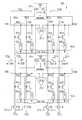
- FIG. 2illustrates a memory device 200 comprising a plurality of memory arrays 150 a , 150 b .
- sense amplifiers 300 a and 300 b in FIG. 2have identical circuitry to sense amplifier 300 of FIG. 3.
- a lower case alphabetic suffixis generally used to discriminate between different units of the same type.
- Each memory array 150 a , 150 bincludes a plurality of memory cells 100 a - 100 d , 100 e - 100 h arranged by tiling a plurality of memory cells 100 together so that the memory cells 100 along any given bit line 104 a , 104 a ′, 104 b , 104 b ′ do not share a common word line 103 a - 103 d . Conversely, the memory cells 100 along any word line 103 do not share a common bit line 104 a , 104 a ′, 104 b , 104 b ′.
- Each memory arrayhas its own set of bit lines.
- memory array 150 aincludes bit lines 104 a , 104 b
- memory array 150 bincludes bit lines 104 a ′, 104 b ′.
- the bit lines from each adjacent pair of memory arrays 150 a , 150 bare coupled to a common sense amplifier 300 a , 300 b .
- bit lines 104 a , 104 a ′are coupled to sense amplifier 300 a
- bit lines 104 b , 104 b ′are coupled to sense amplifier 300 b .
- the sense amplifiers 300 a , 300 bare used to conduct the sense/refresh portion when a memory cell 100 a - 100 h is read.
- Reading a DRAM memory cellcomprises the operations of accessing and sensing/refreshing.
- the purpose of the access operationis to transfer charge stored on the capacitor 102 to the bit line 104 associated with the memory cell 100 .
- the access operationbegins by precharging each bit line 104 a , 104 a ′, 104 b , 104 b ′ to a predetermined potential (e.g., Vcc/2) by coupling each bit line 104 a , 104 b to a potential source (not illustrated). Each bit line 104 a , 104 b is then electrically disconnected.
- a predetermined potentiale.g., Vcc/2
- bit lines 104 a , 104 a ′, 104 b , 104 b ′will float at the predetermined potential due to the inherent capacitance of the bit lines 104 a , 104 a ′, 104 b , 104 b ′.
- the word linee.g., 103 a
- a memory cell being reade.g., 100 a
- the word lineis activated by raising its potential to a level which causes each transistor 101 a , 101 e coupled to the word line 103 a to gate.
- Activation of the word line 103 acauses each capacitor 102 a , 102 e of each memory cell 100 a , 100 e coupled to that word line 103 a to share its charge with its associated bit line 104 a , 104 b .
- the bit lines 104 a ′, 104 b ′ in the other array 150 bremain at the pre-charge potential.
- the charge sharingcauses the bit line 104 a , 104 b potential to either increase or decrease, depending upon the charge stored in the capacitors 102 a , 102 e .
- bit lines 104 a , 104 b of one memory arrayhas its potential altered, at each sense amplifier 300 a , 300 b , a differential potential develops between the bit lines 104 a , 104 b associated with the activated word line 103 a and the other bit lines 104 a ′, 104 b ′ associated with the same sense amplifier 300 a , 300 b .
- the access operationcauses the bit lines 104 a , 104 b associated with the cell 100 a being read to have a potential which is either greater than or less than the pre-charged voltage.
- the change in potentialis small and requires amplification before it can be used.
- the sense/refresh operationserves two purposes. First, the sense/refresh operation amplifies the small change in potential to the bit line coupled to the cell which was accessed. If the bit line has a potential which is lower than the pre-charge potential, the bit line will be driven to ground during sensing. Alternatively, if the bit line has a potential which is higher than the pre-charge potential, the bit line will be driven to Vcc during sensing.
- the second purpose of the sense/refresh operationis to restore the state of the charge in the capacitor of the accessed cell to the state it had prior to the access operation. This step is required since the access operation diluted the charge stored on the capacitor by sharing it with the bit line.
- FIG. 3is a detailed illustration of a sense amplifier 300 , which comprises a N-sense amp 310 N and a P-sense amp portion 310 P.
- the N-sense amp 310 N and the P-sense amp 310 Pinclude nodes NLAT* and ACT, respectively. These nodes are coupled to controllable potential sources (not illustrated).
- Node NLAT*is initially biased to the pre-charge potential of the bit lines 104 (e.g., Vcc/2) while node ACT is initially biased to ground.
- the transistors 301 - 304 of the N- and P- sense amps 310 N, 310 Pare switched off.
- the sense/refresh operationis a two phased operation in which the N- sense amp 310 N is triggered before the P- sense amp 310 P.
- the N- sense amp 310 Nis triggered by bringing the potential at node NLAT* from the pre-charge potential (e.g., Vcc/2) towards ground potential.
- the pre-charge potentiale.g., Vcc/2
- the transistor with the gate coupled to the higher voltage bit linebegins to conduct. This causes the lower voltage bit line to discharge towards the voltage of the NLAT* node.
- the lower voltage bit linewill also reach ground potential.
- the other NMOS transistornever conducts since its gate is coupled to the low voltage digit line being discharged towards ground.
- the P- sense amp 310 Pis triggered (after the N- sense amp 310 N has been triggered) by bringing the potential at node ACT from ground towards Vcc. As the potential of the lower voltage bit line approaches ground (caused by the earlier triggering of the N- sense amp 310 N), the PMOS transistor with its gate coupled to the lower potential bit line will begin to conduct. This causes the initially higher potential bit line to be charged to a potential of Vcc. After both the N- and P- sense amps 310 N, 310 P have been triggered, the higher voltage bit line has its potential elevated to Vcc while the lower potential bit line has it potential reduced to ground.
- the process of triggering both sense amps 310 N, 310 Pamplifies the potential difference created by the access operation to a level suitable for use in digital circuits.
- the bit line 104 a associated with the memory cell 100 a being readis driven from the pre-charge potential of Vcc/2 to ground if the memory cell 100 a stored a charge corresponding to a binary 0, or to Vcc if the memory cell 100 a stored a charge corresponding to a binary 1, thereby permitting a comparator (or differential amplifier) 350 a coupled to bit lines 104 a , 104 a ′ to output a binary 0 or 1 consistent with the data stored in the cell 100 a on signal line 351 .
- the charge initially stored on the capacitor 102 a of the accessed cellis restored to its pre-access state.
- a programmable resistance element of such materialcould be programmed (set) to a high resistive state to store, for example, a binary “1” data bit or programmed to a low resistive state to store a binary “0” data bit. The stored data bit could then be retrieved by detecting the magnitude of a readout current switched through the resistive memory element by an access device, thus indicating the stable resistance state it had previously been programmed to.
- chalcogenide glasses fabricated with solid electrolyte such as a metal doped chalcogenidehave been investigated as data storage memory cells for use in memory devices, such as DRAM memory devices.
- the storage cellsare called programmable conductor cells (alternatively, they are also known as programmable metallization cells).
- One characteristic of such a cellis that it typically includes solid metal electrolyte such as a metal doped chalcogenide and a cathode and anode spaced apart on a surface of the fast ion conductor. Application of a voltage across the cathode and anode causes growth of a metal dendrite which changes the resistance and capacitance of the cell which can then be used to store data.
- One particularly promising programmable, bi-stable resistive materialis an alloy system including Ge:Se:Ag.
- a memory element comprised of a chalcogenide materialhas a natural stable high resistive state but can be programmed to a low resistance state by passing a current pulse from a voltage of suitable polarity through the cell. This causes a programmable conductor, also known as a dendrite, to grow between the anode and cathode which lowers the cell resistance.
- a chalcogenide memory elementis simply written over by the appropriate current pulse and voltage polarity (reverse of that which writes the cell to a low resistance state) to reprogram it, and thus does not need to be erased.
- a memory element of chalcogenide materialis nearly nonvolatile, in that it need only be rarely (e.g., once per week) connected to a power supply or refreshed, in order to retain its programmed low resistance state.
- Such memory cellsunlike DRAM cells, can be accessed without requiring a refresh.
- PCRAMprogrammable conductor random access memory
- the present inventionis directed to a method and apparatus for reacting a PCRAM memory cell without refreshing the cell.
- the programmable conductor of the PCRAM cellAt a predetermined time after the programmable conductor of the PCRAM cell has been coupled to its bit line, the programmable conductor is electrically decoupled from the bit line.
- the predetermined timeis chosen to be a point in time before the N- and P- sense amplifiers have been activated. In this manner, the N- and P- sense amplifier can change the potential on the bit line without causing the altered potential to rewrite the PCRAM cell.
- the present inventionmay be practiced by deactivating the word line at the predetermined time after the word line has been activated.
- isolation transistorsmay be added on each bit line between the PCRAM cell and the sense amplifier to decouple the PCRAM cells from their associated bit lines.
- FIG. 1is a schematic diagram of a conventional DRAM cell
- FIG. 2is a schematic diagram of a conventional DRAM array
- FIG. 3is schematic diagram a conventional sense amplifier
- FIG. 4is a schematic diagram of a PCRAM cell
- FIG. 5is a schematic diagram a PCRAM array
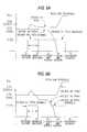
- FIGS. 6A and 6Bare timing diagrams illustrating the voltages on the word and bit lines when a PCRAM cell is read in high resistance and low resistance states, respectively.
- FIG. 7is a flow chart illustrating the method of the invention.
- FIG. 8is a block diagram of a processor based system including a PCRAM in accordance with the principles of the present invention.
- FIG. 9is a schematic diagram of a PCRAM array according to a second embodiment of the present invention.
- FIG. 10is a schematic diagram of an alternative embodiment of a PCRAM cell for use with the PCRAM array of FIG. 9.
- FIG. 4a PCRAM cell 400 and in FIG. 5 a memory device 500 a memory device comprised of a plurality of PCRAM cells 400 a - 400 h .
- a PCRAM cell 400comprises an access transistor 401 , a programmable conductor memory element 402 , and a cell plate 403 .
- the access transistor 401has its gate coupled to a word line 405 and one terminal coupled to a bit line 406 .
- a small portion of an array of such cellsis shown in FIG.
- the bit lines 406 a , 406 bare coupled to a respective pre-charge circuits 501 a , 105 b , which can switchably supply a pre-charge potential to the bit lines 406 a , 406 a ′, 406 b , 406 b ′.
- the other terminal of the access transistor 401is coupled to one end of the programmable conductor memory element 402 , while the other end of the programmable conductor memory element 402 is coupled to a cell plate 403 .
- the cell plate 403may span and be coupled to several other PCRAM cells.
- the cell plating 403is also coupled to a potential source. In the exemplary embodiment the potential source is at 1.25 volts (Vdd/2).
- the access transistor 401as well as the other access transistors, are depicted as N-type CMOS transistors, however, it should be understood that P-type CMOS transistors may be used as long as the corresponding polarities of the other components and voltages are modified accordingly.
- the programmable conductor memory element 402is preferably made of chalcogenide, however, it should be understood that any other bi-stable resistive material known to those with ordinary skill in the art may also be used. In the exemplary embodiment, the programmable conductor memory element 402 stores a binary 0 when has a resistance of approximately 10 K ohm, and a binary 1 when it has a resistance greater than 10 M ohm.
- the programmable conductoris ideally programmed to store a low resistance, e.g., binary 0, by a voltage of +0.25 volt and can be restored to a high resistance value, e.g., a binary 1, by a programming voltage of ⁇ 0.25 volt.
- the programmable conductorcan be nondestructively read by a reading voltage having a magnitude of less than 0.25 volt. In the exemplary embodiment, the reading voltage is 0.2 volt.
- alternate parametersmay be selected for the PCRAM cell without departing from the spirit and scope of the invention.
- FIG. 5illustrates a memory device 500 comprising a plurality of memory arrays 550 a , 550 b .
- Each memory array 550 a , 550 bincludes a plurality of memory cells 400 a - 400 d , 400 e - 400 h arranged by tiling a plurality of memory cells 400 together so that the memory cells 400 along any given bit line 406 a , 406 a ′, 406 b , 406 b ′ do not share a common word line 405 a - 405 d .
- each word lineis switchably to a word line driver 512 a - 512 d via a transistor 510 a - 510 d . Additionally, each word line may also be switchably coupled to ground via transistors 520 a - 520 d .
- Each memory array 550 a , 550 bhas its own set of bit lines.
- memory array 550 aincludes bit lines 406 a , 406 b
- memory array 550 bincludes bit lines 406 a ′, 406 b ′.
- bit lines from each adjacent pair of memory arrays 550 a , 550 bare coupled to a common sense amplifier 600 a , 600 b .
- bit lines 406 a , 406 a ′are coupled to sense amplifier 600 a
- bit lines 406 b , 406 b ′are coupled to sense amplifier 600 b .
- FIG. 5illustrates a memory device having only two arrays 550 a , 550 b , and eight cells 400 a - 400 h .
- real world memory deviceswould have signficantly more cells and arrays.
- a real world memory devicemay include several million cells 400 .
- the memory device 500also includes a plurality of pre-charge circuits 501 a - 501 b .
- One pre-charge circuit(e.g., 501 a ) is provided for each pair of bit lines coupled to a sense amplifier (e.g., 406 a , 406 a ′).
- Each pre-charge circuit(e.g., 501 a ) includes two transistors (e.g., 501 a , 501 b ). One terminal of each transistor is coupled to a potential source. In the exemplary embodiment, the potential source is at 2.5 volts (Vdd).
- each transistore.g., 502 a , 502 b
- the gate of the each transistoris coupled to a pre-charge control signal.
- the transistorse.g., 502 a , 502 b
- the transistorsare P-MOS type transistor.
- the transistorsconducts, thereby pre-charging the bit lines (e.g., 406 a , 406 a ′).
- the transistorse.g., 502 a , 502 b
- the transistorsare switched off. Due to capacitance inherent in the bit lines (e.g., 406 a , 406 a ′), the bit lines will remain at approximately the pre-charge voltage level of 2.5 volts for a predetermined period of time.
- Reading a PCRAM cell, for example, cell 400 a , in the PCRAM device 500comprises the operations of accessing and sensing.
- the purpose of the access operationis to create a small potential difference between the bit lines (e.g., 406 a , 406 a ′) coupled to the same sense amplifier (e.g., 300 a ) of the memory cell 400 a being read.
- This small potential differencecan be subsequently amplified by a sense amplifier 300 to the threshold required to subsequently drive a comparator coupled to the bit lines to output a value corresponding to the contents of the memory cell 400 a .
- the access operationbegins with the pre-charging of the bit lines 406 a , 406 a ′, 406 b , 406 b ′ of the memory device 500 via pre-charge circuits 501 a - 501 b (step S 1 ).
- the bit linesmay be pre-charged by temporarily bringing the pre-charge signal low, causing transistors 502 a - 502 d to conduct the pre-charge voltage (Vdd) to the bit lines 406 a , 406 a ′, 406 b , 406 b ′.
- the transistors 502 a - 502 dstop conducting, but the bit lines 406 a , 406 a ′, 406 b , 406 b ′ will remain at the pre-charge potential for a predetermined period due to the capacitance inherent in the bit lines.
- bit lines 406 a , 406 a ′, 406 b , 406 b ′are pre-charged to 2.5 volts and the cell plate 403 a , 403 b is tied to 1.25 volts.
- the 1.25 volt potential difference between the bit line and the cell platewill cause the bit line to discharge to the cell plate through the access transistor 401 (when it is in a conductive state) and the programmable conductor memory element 402 .
- the discharge rateis dependent upon the resistive state of the programmable conductor memory element 402 . That is, a low resistive state will cause the bit line to discharge faster than a high resistive state. As the bit line discharges, its voltage will fall from the pre-charge voltage toward the cell plate voltage.
- the word lines 405 a - 405 dare normally at ground potential.
- the access transistors 401 a - 401 eare normally switched off.
- the word line 405 a associated with the cell 400 a to be readis activated by bringing its potential from ground to a predetermined level (step S 2 ).
- the predetermined levelis designed to create a reading voltage at the programmable contact 402 a , which as previously explained, must have a magnitude less than the magnitude of a writing voltage.
- the word line 401 ais brought to 2.25 volt.
- the threshold voltage of the transistor 401 ais 0.8 volt
- the potential at the interface between the transistor 401 a and the programmable contact 402 ais 1.45 volt. This results in a reading voltage of 0.2 volt since the voltage at the interface between the programmable contact 402 a and the cell plate 403 a is maintained at 1.25 volt.
- bit lines 406 aDue to the inherent parasitic capacitance between the word line 401 a and its associated bit lines 406 a the potential in the associated bit line 406 a increase as the word line 401 a is activated. In the exemplary embodiment, the potential in bit line 406 a increases by 0.1 volt to 2.6 volt. It should be noted that the word lines 405 c , 405 d coupled to complementary bit lines 406 a ′, 406 b ′ remain at ground potential. Thus, bit lines 406 a ′, 406 b ′ remain at the pre-charge potential, which is 2.5 volt in the exemplary embodiment.
- bit line 406 ais used in combination with the two bi-stable resistive states of the programmable contact 402 a to cause one of the bit lines (e.g., 406 a ) coupled to a sense amplifier (e.g., 300 a ) to have either a greater or lesser voltage than the other bit line (e.g., 406 a ′) coupled to the same sense amplifier 300 a .
- the parasitic capacitance between word lines and associated bit linesis used to achieve an initial state where the bit line (e.g., 406 a ) associated with the cell 400 a being read is at a higher potential than the other bit line 406 a ′ coupled to the same sense amplifier 300 a .
- the memoryis designed and operated so that if the programmable contact 402 a has a high resistive state, bit line 406 a discharges slowly, thereby causing it to maintain its relatively higher potential. However, if the programmable contact 402 a has a low resistive state, bit line 406 a discharges at a faster rate, so that bit line 406 transitions to a lower potential state than bit line 406 a ′.
- step S 3the word line 405 a associated with the cell 400 a being read is deactivated by returning its potential to ground (step S 4 ).
- Word line deactivationmay be achieved by, for example, grounding terminal 511 a , which will cause the transistor 510 a serially coupling the word line driver 512 a to the word line 405 a to stop conducting. This shuts off access transistors 401 a , 401 thereby preventing further discharge of the bit line through the programmable contact 402 a , 402 e .
- the word linecan be held high for a longer period of time. This mode of operation is shown via the dashed trace in FIGS. 6A and 6B.
- T 2may be varied without departing from spirit of the invention.
- the objectives of the present inventionwill be realized by electrically decoupling the programmable contact from the bit line at any time before the bit line voltages are amplified by the sense amplifiers 310 N, 310 P to a level which result in the potential difference across the programmable contact reaching threshold required to write the programmable contact.
- FIGS. 6A and 6Billustrate T 2 occurring prior to either sense amplifiers 310 N, 310 P being activated, depending upon the electrical characteristics of the memory device 500 , T 2 may occur, for example, between the activation of the N- sense amp 310 N and the P- sense amp 310 P.
- the predetermined time tmust be sufficiently long to permit the logical state of the programmable conductor 402 a to be reflected on the bit line 406 a ; i.e., the bit line 406 a voltage to be sufficiently altered from the pre-charge voltage by the discharge through the programmable conductor 402 a so that the two resistive states of the programmable conductor 402 a can be distinguished and amplified by the sense amplifier 300 a.
- the N- sense amplifier 310 Nis activated (start of step S 5 ).
- activating the N-sense amplifiercauses the bit line (e.g., 406 a ′) having the lower potential to be pulled with the NLAT signal toward ground.
- T 3is approximately 30 nanosecond after T 1 .
- the value T 3may be varied without departing from spirit of the invention.
- T 4the P- sense amplifier 310 P is activated. As previously noted with respect to DRAM systems, activating the P-sense amplifier causes the bit line (e.g., 406 a ) having the higher potential to be pulled towards Vcc. In the exemplary embodiment, T 4 is approximately 35 nanosecond after T 1 (end of step S 5 ). However, it should be noted that the value of T 4 may be varied without departing from spirit of the invention.
- the sense amplifier 300 a associated with the cell 400 a being readwill have one of its bit lines (e.g., 406 a ) at Vcc potential and the other bit line (e.g., 406 a ′) at ground potential. Since one bit line coupled to sense amplifier 300 a is now at ground potential while the other bit line is now at Vcc potential, a comparator (or differential amplifier) 350 can be used to output a value corresponding to the contents of the cell 400 a on signal line 351 a.
- FIG. 9is an illustration of a memory device 900 according to an alternate embodiment of the present invention.
- This alternate embodimentis designed for use with PCRAM cells which do not include an access transistor 401 .
- FIG. 10illustrates one example of a PCRAM cell 400 ′ which utilizes a pair of diodes 1001 a , 1001 b in lieu of an access transistor.
- the PCRAM cell 400 ′features a programmable conductor memory element 402 which is coupled to a bit line 104 .
- the programmable conductor memory element 402is also coupled to the word line via a diode circuit 1002 .
- the diode circuitcomprises two diodes 1001 a , 1001 b arranged as shown.
- the memory device 900is otherwise very similar to the memory device 500 of the first embodiment.
- memory device 900includes new isolation transistors 901 a - 901 d which serially connect the sense amplifiers 300 a , 300 d to the bit lines 406 a , 406 a ′, 406 b , 406 b ′.
- the inventionoperates in memory device 900 in a manner very similar to memory device 500 except that instead of deactivating word lines 405 a to electrically decouple memory cell 400 a from amplified voltages on the bit line 406 a ′ prior to sensing, the isolation transistor 901 a , which is normally conducting, is turned off, thereby bifurcating the bit line 406 a .
- the portion of the bit line between the transistor 901 a and the sense amplifier 301 awill then be sensed while the portion of the bit line between the transistor 901 a and the pre-charge circuit 501 a will be isolated from the sense amplifier.
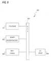
- FIG. 8is a block diagram of a processor based system 800 , such as a computer system, containing a PCRAM semiconductor memory 802 as described in connection with the other figures.
- the memory 802may be constituted as one or more memory chips or memory integrated circuits mounted on a memory module, for example, a plug-in memory module such as a SIMM, DIMM, or other plug-in memory module.
- the processor based system 800includes a processor 801 , a memory 802 , a mass storage 803 , and an I/O device 804 , each coupled to a bus 805 .
- processor 801could be any type of processor and may include multiple processor and/or processors and co-processors.
- Memory 802is illustrated in FIG. 9 as having a plurality of PCRAM chips 500 . However, memory 802 may only include a single PCRAM device 500 , or a larger plurality of PCRAM devices 500 than illustrated, and/or may include additional forms of memories, such as non-volatile memory or cache memories. While one mass storage 803 device is illustrated, the processor based system 800 may include a plurality of mass storage devices, possibly of varying types such as, but not limited to, floppy disks, CDROMs, CD-R, CD-RW, DVD, hard disks, and disk arrays.
- I/O device 804may likewise comprise a plurality of I/O devices of varying types, including, but not limited to keyboard, mouse, graphic cards, monitors, and network interfaces.
- Bus 805while illustrated as a single bus may comprise a plurality of buses and/or bridges, which may be coupled to each other or bridged by other components. Some of the devices 801 - 804 may be coupled to only a single bus 805 , others may be coupled to a plurality of buses 805 .
- the present inventionprovides a PCRAM cell 400 and a method for reading the contents of the cell 400 using sense amplifiers but without rewriting the contents of the cell.
- Rewrite preventionis achieved by isolating the programmable conductor 402 of the cell 400 from the bit line 406 a predetermined amount of time after the programmable conductor 402 has been electrically coupled to the bit line 406 .
- the predetermined amount of timecorresponds a time prior to the activation time of both the N- and P- sense amps 310 N, 310 P.
- the PCRAM cell 400includes an access transistor 401 for electrically coupling and decoupling the cell to the bit line.
- the access transistor 401has a gate coupled to a word line.
- the word lineis deactivated the predetermined amount of time after it has been activated, thereby ensuring that the activation of the N- and P- sense amplifiers 310 N, 310 P do not rewrite the cell 400 .
- the PCRAM cell 400does not include an access transistor.
- the PCRAM cellinstead utilize diodes.
- isolation transistormay be inserted between the programmable contact memory element and the bit line associated with the programmable contact memory element.
- the isolation transistorswhich are normally conducting, may be switched off at the same predetermined time as in the exemplary embodiment, after the word line has been activated, thereby achieving the same result of isolating the programmable contact memory element from the elevated voltages generated during sensing.
Landscapes
- Engineering & Computer Science (AREA)
- Microelectronics & Electronic Packaging (AREA)
- Computer Hardware Design (AREA)
- Chemical & Material Sciences (AREA)
- Crystallography & Structural Chemistry (AREA)
- Dram (AREA)
- Pharmaceuticals Containing Other Organic And Inorganic Compounds (AREA)
- Electrochromic Elements, Electrophoresis, Or Variable Reflection Or Absorption Elements (AREA)
Abstract
Description
- The present invention relates to integrated memory circuits. More specifically, it relates to a method for reading a programmable conductor random access memory (PCRAM) cell.[0001]
- Dynamic random access memory (DRAM) integrated circuit arrays have existed for more than thirty years and their dramatic increase in storage capacity has been achieved through advances in semiconductor fabrication technology and circuit design technology. The tremendous advances in these two technologies have also achieved higher levels of integration that permit dramatic reductions in memory array size and cost, as well as increased process yield.[0002]
- FIG. 1 is a schematic diagram of a[0003]
DRAM memory cell 100 comprising anaccess transistor 101 and acapacitor 102. Thecapacitor 102, which is coupled to a Vcc/2 potential source and thetransistor 101, stores one bit of data in the form of a charge. Typically, a charge of one polarity (e.g., a charge corresponding to a potential difference across thecapacitor 102 of +Vcc/2) is stored in thecapacitor 102 to represent a binary “1” while a charge of the opposite polarity (e.g., a charge corresponding to a potential difference across thecapacitor 102 of −Vcc/2) represents a binary “0.” The gate of thetransistor 101 is coupled to aword line 103, thereby permitting theword line 103 to control whether thecapacitor 102 is conductively coupled via thetransistor 101 to abit line 104. The default state of eachword line 103 is at ground potential, which causes thetransistor 101 to be switched off, thereby electrically isolatingcapacitor 102. - One of the drawbacks associated with[0004]
DRAM cells 100 is that the charge on thecapacitor 102 may naturally decay over time, even if thecapacitor 102 remains electrically isolated. Thus,DRAM cells 100 require periodic refreshing. Additionally, as discussed below, refreshing is also required after amemory cell 100 has been accessed, for example, as part of a read operation. - FIG. 2 illustrates a[0005]
memory device 200 comprising a plurality ofmemory arrays sense amplifiers memory array memory cells 100a-100d,100e-100harranged by tiling a plurality ofmemory cells 100 together so that thememory cells 100 along any givenbit line common word line 103a-103d. Conversely, thememory cells 100 along anyword line 103 do not share acommon bit line memory array 150aincludesbit lines memory array 150bincludesbit lines 104a′,104b′. The bit lines from each adjacent pair ofmemory arrays common sense amplifier bit lines sense amplifier 300a, whilebit lines amplifier 300b. As explained below, thesense amplifiers memory cell 100a-100his read. - Reading a DRAM memory cell comprises the operations of accessing and sensing/refreshing.[0006]
- The purpose of the access operation is to transfer charge stored on the[0007]
capacitor 102 to thebit line 104 associated with thememory cell 100. The access operation begins by precharging eachbit line bit line bit line bit lines bit lines transistor word line 103ato gate. It should be noted that due to inherent parasitic capacitance betweenbit lines 104 andword lines 103, activation of aword line 103 will cause the potential at each associatedbit line 104 to increase slightly. However, in typical DRAM systems, the magnitude of this potential change is insignificant in comparison to the magnitude of the potential change on the bit lines due to charge sharing. Therefore, with respect to DRAM systems only, further discussion regarding the effect of parasitic capacitance is omitted. - Activation of the[0008]
word line 103acauses eachcapacitor memory cell word line 103ato share its charge with its associatedbit line bit lines 104a′,104b′ in theother array 150bremain at the pre-charge potential. The charge sharing causes thebit line capacitors bit lines sense amplifier bit lines activated word line 103aand theother bit lines 104a′,104b′ associated with thesame sense amplifier bit lines cell 100abeing read to have a potential which is either greater than or less than the pre-charged voltage. However, the change in potential is small and requires amplification before it can be used. - The sense/refresh operation serves two purposes. First, the sense/refresh operation amplifies the small change in potential to the bit line coupled to the cell which was accessed. If the bit line has a potential which is lower than the pre-charge potential, the bit line will be driven to ground during sensing. Alternatively, if the bit line has a potential which is higher than the pre-charge potential, the bit line will be driven to Vcc during sensing. The second purpose of the sense/refresh operation is to restore the state of the charge in the capacitor of the accessed cell to the state it had prior to the access operation. This step is required since the access operation diluted the charge stored on the capacitor by sharing it with the bit line.[0009]
- FIG. 3 is a detailed illustration of a sense amplifier[0010]300, which comprises a N-
sense amp 310N and a P-sense amp portion 310P. The N-sense amp 310N and the P-sense amp 310P include nodes NLAT* and ACT, respectively. These nodes are coupled to controllable potential sources (not illustrated). Node NLAT* is initially biased to the pre-charge potential of the bit lines104 (e.g., Vcc/2) while node ACT is initially biased to ground. In this initial state, the transistors301-304 of the N- and P-sense amps sense amp 310N is triggered before the P-sense amp 310P. - The N-[0011]
sense amp 310N is triggered by bringing the potential at node NLAT* from the pre-charge potential (e.g., Vcc/2) towards ground potential. As the potential difference between node NLAT* and thebit lines NMOS transistors - The P-[0012]
sense amp 310P is triggered (after the N-sense amp 310N has been triggered) by bringing the potential at node ACT from ground towards Vcc. As the potential of the lower voltage bit line approaches ground (caused by the earlier triggering of the N-sense amp 310N), the PMOS transistor with its gate coupled to the lower potential bit line will begin to conduct. This causes the initially higher potential bit line to be charged to a potential of Vcc. After both the N- and P-sense amps sense amps bit line 104aassociated with thememory cell 100abeing read is driven from the pre-charge potential of Vcc/2 to ground if thememory cell 100astored a charge corresponding to a binary 0, or to Vcc if thememory cell 100astored a charge corresponding to a binary 1, thereby permitting a comparator (or differential amplifier)350acoupled tobit lines cell 100aonsignal line 351. Additionally, the charge initially stored on thecapacitor 102aof the accessed cell is restored to its pre-access state. - Efforts continue to identify other forms of memory elements for use in memory cells. Recent studies have focused on resistive materials that can be programmed to exhibit either high or low stable ohmic states. A programmable resistance element of such material could be programmed (set) to a high resistive state to store, for example, a binary “1” data bit or programmed to a low resistive state to store a binary “0” data bit. The stored data bit could then be retrieved by detecting the magnitude of a readout current switched through the resistive memory element by an access device, thus indicating the stable resistance state it had previously been programmed to.[0013]
- Recently chalcogenide glasses fabricated with solid electrolyte such as a metal doped chalcogenide have been investigated as data storage memory cells for use in memory devices, such as DRAM memory devices. U.S. Pat. Nos. 5,761,115, 5,896,312, 5,914,893, and 6,084,796 all describe this technology and are incorporated herein by reference. The storage cells are called programmable conductor cells (alternatively, they are also known as programmable metallization cells). One characteristic of such a cell is that it typically includes solid metal electrolyte such as a metal doped chalcogenide and a cathode and anode spaced apart on a surface of the fast ion conductor. Application of a voltage across the cathode and anode causes growth of a metal dendrite which changes the resistance and capacitance of the cell which can then be used to store data.[0014]
- One particularly promising programmable, bi-stable resistive material is an alloy system including Ge:Se:Ag. A memory element comprised of a chalcogenide material has a natural stable high resistive state but can be programmed to a low resistance state by passing a current pulse from a voltage of suitable polarity through the cell. This causes a programmable conductor, also known as a dendrite, to grow between the anode and cathode which lowers the cell resistance. A chalcogenide memory element is simply written over by the appropriate current pulse and voltage polarity (reverse of that which writes the cell to a low resistance state) to reprogram it, and thus does not need to be erased. Moreover, a memory element of chalcogenide material is nearly nonvolatile, in that it need only be rarely (e.g., once per week) connected to a power supply or refreshed, in order to retain its programmed low resistance state. Such memory cells, unlike DRAM cells, can be accessed without requiring a refresh.[0015]
- While conventional sense amp circuitry, such as those associated with DRAM cells, are capable of sensing programmable conductor random access memory (PCRAM) cells, the natural refresh operation associated with these sense amplifiers are not required in a PCRAM context. Indeed, frequent rewriting of PCRAM cells is not desirable because it can cause the PCRAM cell to become resistant to rewriting. Accordingly, there is a need and desire for a circuit and method for reading PCRAM cells without refreshing them.[0016]
- The present invention is directed to a method and apparatus for reacting a PCRAM memory cell without refreshing the cell. At a predetermined time after the programmable conductor of the PCRAM cell has been coupled to its bit line, the programmable conductor is electrically decoupled from the bit line. The predetermined time is chosen to be a point in time before the N- and P- sense amplifiers have been activated. In this manner, the N- and P- sense amplifier can change the potential on the bit line without causing the altered potential to rewrite the PCRAM cell. In PCRAM arrays which use access transistors having gates coupled to word lines, the present invention may be practiced by deactivating the word line at the predetermined time after the word line has been activated. In PCRAM arrays which do not include access transistors, isolation transistors may be added on each bit line between the PCRAM cell and the sense amplifier to decouple the PCRAM cells from their associated bit lines.[0017]
- The foregoing and other advantages and features of the invention will become more apparent from the detailed description of exemplary embodiments of the invention given below with reference to the accompanying drawings in which:[0018]
- FIG. 1 is a schematic diagram of a conventional DRAM cell;[0019]
- FIG. 2 is a schematic diagram of a conventional DRAM array;[0020]
- FIG. 3 is schematic diagram a conventional sense amplifier;[0021]
- FIG. 4 is a schematic diagram of a PCRAM cell;[0022]
- FIG. 5 is a schematic diagram a PCRAM array;[0023]
- FIGS. 6A and 6B are timing diagrams illustrating the voltages on the word and bit lines when a PCRAM cell is read in high resistance and low resistance states, respectively.[0024]
- FIG. 7 is a flow chart illustrating the method of the invention;[0025]
- FIG. 8 is a block diagram of a processor based system including a PCRAM in accordance with the principles of the present invention;[0026]
- FIG. 9 is a schematic diagram of a PCRAM array according to a second embodiment of the present invention; and[0027]
- FIG. 10 is a schematic diagram of an alternative embodiment of a PCRAM cell for use with the PCRAM array of FIG. 9.[0028]
- Now referring to the drawings, where like reference numerals designate like elements, there is shown in FIG. 4 a[0029]
PCRAM cell 400 and in FIG. 5 a memory device500 a memory device comprised of a plurality ofPCRAM cells 400a-400h. As illustrated in FIG. 4, aPCRAM cell 400 comprises anaccess transistor 401, a programmableconductor memory element 402, and acell plate 403. Theaccess transistor 401 has its gate coupled to aword line 405 and one terminal coupled to abit line 406. A small portion of an array of such cells is shown in FIG. 5 as includingbit lines word lines bit lines pre-charge circuits 501a,105b, which can switchably supply a pre-charge potential to thebit lines access transistor 401 is coupled to one end of the programmableconductor memory element 402, while the other end of the programmableconductor memory element 402 is coupled to acell plate 403. Thecell plate 403 may span and be coupled to several other PCRAM cells. The cell plating403 is also coupled to a potential source. In the exemplary embodiment the potential source is at 1.25 volts (Vdd/2). - The[0030]
access transistor 401, as well as the other access transistors, are depicted as N-type CMOS transistors, however, it should be understood that P-type CMOS transistors may be used as long as the corresponding polarities of the other components and voltages are modified accordingly. The programmableconductor memory element 402 is preferably made of chalcogenide, however, it should be understood that any other bi-stable resistive material known to those with ordinary skill in the art may also be used. In the exemplary embodiment, the programmableconductor memory element 402 stores a binary 0 when has a resistance of approximately 10 K ohm, and a binary 1 when it has a resistance greater than 10 M ohm. The programmable conductor is ideally programmed to store a low resistance, e.g., binary 0, by a voltage of +0.25 volt and can be restored to a high resistance value, e.g., a binary 1, by a programming voltage of −0.25 volt. The programmable conductor can be nondestructively read by a reading voltage having a magnitude of less than 0.25 volt. In the exemplary embodiment, the reading voltage is 0.2 volt. However, it should be readily apparent that alternate parameters may be selected for the PCRAM cell without departing from the spirit and scope of the invention. - FIG. 5 illustrates a[0031]
memory device 500 comprising a plurality ofmemory arrays memory array memory cells 400a-400d,400e-400harranged by tiling a plurality ofmemory cells 400 together so that thememory cells 400 along any givenbit line common word line 405a-405d. Conversely, thememory cells 400 along anyword line 405a-405ddo not share acommon bit line word lines 405a-405dto/from the word line drivers512a-512b/ground. Eachmemory array memory array 550aincludesbit lines memory array 550bincludesbit lines 406a′,406b′. The bit lines from each adjacent pair ofmemory arrays bit lines bit lines arrays cells 400a-400h. However, it should be understood that real world memory devices would have signficantly more cells and arrays. For example, a real world memory device may include several millioncells 400. - The[0032]
memory device 500 also includes a plurality of pre-charge circuits501a-501b. One pre-charge circuit (e.g.,501a) is provided for each pair of bit lines coupled to a sense amplifier (e.g.,406a,406a′). Each pre-charge circuit (e.g.,501a) includes two transistors (e.g.,501a,501b). One terminal of each transistor is coupled to a potential source. In the exemplary embodiment, the potential source is at 2.5 volts (Vdd). Another terminal of each transistor (e.g.,502a,502b) is coupled to its corresponding bit line (e.g.,406a,406a′, respectively). The gate of the each transistor (e.g.,502a,502b) is coupled to a pre-charge control signal. As illustrated, the transistors (e.g.,502a,502b) are P-MOS type transistor. Thus, when the pre-charge signal is low, the transistors (e.g.,502a,502b) conducts, thereby pre-charging the bit lines (e.g.,406a,406a′). When the pre-charge signal is high, the transistors (e.g.,502a,502b) are switched off. Due to capacitance inherent in the bit lines (e.g.,406a,406a′), the bit lines will remain at approximately the pre-charge voltage level of 2.5 volts for a predetermined period of time. - Reading a PCRAM cell, for example,[0033]
cell 400a, in thePCRAM device 500 comprises the operations of accessing and sensing. - The purpose of the access operation is to create a small potential difference between the bit lines (e.g.,[0034]406a,406a′) coupled to the same sense amplifier (e.g.,300a) of the
memory cell 400abeing read. This small potential difference can be subsequently amplified by a sense amplifier300 to the threshold required to subsequently drive a comparator coupled to the bit lines to output a value corresponding to the contents of thememory cell 400a. Now also referring to FIG. 7, the access operation begins with the pre-charging of thebit lines memory device 500 via pre-charge circuits501a-501b(step S1). The bit lines may be pre-charged by temporarily bringing the pre-charge signal low, causing transistors502a-502dto conduct the pre-charge voltage (Vdd) to thebit lines bit lines - In the exemplary embodiment,[0035]
bit lines cell plate conductor memory element 402. The discharge rate is dependent upon the resistive state of the programmableconductor memory element 402. That is, a low resistive state will cause the bit line to discharge faster than a high resistive state. As the bit line discharges, its voltage will fall from the pre-charge voltage toward the cell plate voltage. - In the[0036]
memory device 500, theword lines 405a-405dare normally at ground potential. Thus theaccess transistors 401a-401eare normally switched off. Now also referring to FIGS. 6A and 6B, at time T1, theword line 405aassociated with thecell 400ato be read is activated by bringing its potential from ground to a predetermined level (step S2). The predetermined level is designed to create a reading voltage at theprogrammable contact 402a, which as previously explained, must have a magnitude less than the magnitude of a writing voltage. In the exemplary embodiment, theword line 401ais brought to 2.25 volt. Since the threshold voltage of thetransistor 401ais 0.8 volt, the potential at the interface between thetransistor 401aand theprogrammable contact 402ais 1.45 volt. This results in a reading voltage of 0.2 volt since the voltage at the interface between theprogrammable contact 402aand thecell plate 403ais maintained at 1.25 volt. - Due to the inherent parasitic capacitance between the[0037]
word line 401aand its associatedbit lines 406athe potential in the associatedbit line 406aincrease as theword line 401ais activated. In the exemplary embodiment, the potential inbit line 406aincreases by 0.1 volt to 2.6 volt. It should be noted that the word lines405c,405dcoupled tocomplementary bit lines 406a′,406b′ remain at ground potential. Thus,bit lines 406a′,406b′ remain at the pre-charge potential, which is 2.5 volt in the exemplary embodiment. - The increased potential of[0038]
bit line 406ais used in combination with the two bi-stable resistive states of theprogrammable contact 402ato cause one of the bit lines (e.g.,406a) coupled to a sense amplifier (e.g.,300a) to have either a greater or lesser voltage than the other bit line (e.g.,406a′) coupled to thesame sense amplifier 300a. Essentially, the parasitic capacitance between word lines and associated bit lines is used to achieve an initial state where the bit line (e.g.,406a) associated with thecell 400abeing read is at a higher potential than theother bit line 406a′ coupled to thesame sense amplifier 300a. The memory is designed and operated so that if theprogrammable contact 402ahas a high resistive state,bit line 406adischarges slowly, thereby causing it to maintain its relatively higher potential. However, if theprogrammable contact 402ahas a low resistive state,bit line 406adischarges at a faster rate, so thatbit line 406 transitions to a lower potential state thanbit line 406a′. These two effects can be seen by comparing FIG. 6A (illustrating the effects of a programmable contact at a high resistive state) and FIG. 6B (illustrating the effects of a programmable contact at a low resistive state.) - At time T[0039]2, a predetermined time t after time T1 (step S3), the
word line 405aassociated with thecell 400abeing read is deactivated by returning its potential to ground (step S4). Word line deactivation may be achieved by, for example, grounding terminal511a, which will cause thetransistor 510aserially coupling theword line driver 512ato theword line 405ato stop conducting. This shuts offaccess transistors programmable contact programmable contact programmable contact - It should be noted that the values of t and T[0040]2 may be varied without departing from spirit of the invention. In particular, the objectives of the present invention will be realized by electrically decoupling the programmable contact from the bit line at any time before the bit line voltages are amplified by the
sense amplifiers sense amplifiers memory device 500, T2 may occur, for example, between the activation of the N-sense amp 310N and the P-sense amp 310P. Regardless, the predetermined time t must be sufficiently long to permit the logical state of theprogrammable conductor 402ato be reflected on thebit line 406a; i.e., thebit line 406avoltage to be sufficiently altered from the pre-charge voltage by the discharge through theprogrammable conductor 402aso that the two resistive states of theprogrammable conductor 402acan be distinguished and amplified by thesense amplifier 300a. - At time period T[0041]3, the N-
sense amplifier 310N is activated (start of step S5). As previously noted with respect to DRAM systems, activating the N-sense amplifier causes the bit line (e.g.,406a′) having the lower potential to be pulled with the NLAT signal toward ground. In the exemplary embodiment, T3 is approximately 30 nanosecond after T1. However, it should be noted that the value T3 may be varied without departing from spirit of the invention. - At time period T[0042]4, the P-
sense amplifier 310P is activated. As previously noted with respect to DRAM systems, activating the P-sense amplifier causes the bit line (e.g.,406a) having the higher potential to be pulled towards Vcc. In the exemplary embodiment, T4 is approximately 35 nanosecond after T1 (end of step S5). However, it should be noted that the value of T4 may be varied without departing from spirit of the invention. - At time T[0043]5, the
sense amplifier 300aassociated with thecell 400abeing read will have one of its bit lines (e.g.,406a) at Vcc potential and the other bit line (e.g.,406a′) at ground potential. Since one bit line coupled tosense amplifier 300ais now at ground potential while the other bit line is now at Vcc potential, a comparator (or differential amplifier)350 can be used to output a value corresponding to the contents of thecell 400aonsignal line 351a. - FIG. 9 is an illustration of a[0044]
memory device 900 according to an alternate embodiment of the present invention. This alternate embodiment is designed for use with PCRAM cells which do not include anaccess transistor 401. For example, FIG. 10 illustrates one example of aPCRAM cell 400′ which utilizes a pair ofdiodes PCRAM cell 400′ features a programmableconductor memory element 402 which is coupled to abit line 104. The programmableconductor memory element 402 is also coupled to the word line via adiode circuit 1002. The diode circuit comprises twodiodes - The[0045]
memory device 900 is otherwise very similar to thememory device 500 of the first embodiment. However,memory device 900 includes new isolation transistors901a-901dwhich serially connect thesense amplifiers 300a,300dto thebit lines memory device 900 in a manner very similar tomemory device 500 except that instead of deactivatingword lines 405ato electrically decouplememory cell 400afrom amplified voltages on thebit line 406a′ prior to sensing, theisolation transistor 901a, which is normally conducting, is turned off, thereby bifurcating thebit line 406a. The portion of the bit line between thetransistor 901aand the sense amplifier301awill then be sensed while the portion of the bit line between thetransistor 901aand thepre-charge circuit 501awill be isolated from the sense amplifier. - FIG. 8 is a block diagram of a processor based[0046]
system 800, such as a computer system, containing aPCRAM semiconductor memory 802 as described in connection with the other figures. Thememory 802 may be constituted as one or more memory chips or memory integrated circuits mounted on a memory module, for example, a plug-in memory module such as a SIMM, DIMM, or other plug-in memory module. The processor basedsystem 800 includes aprocessor 801, amemory 802, amass storage 803, and an I/O device 804, each coupled to abus 805. While asingle processor 801 is illustrated, it should be understood thatprocessor 801 could be any type of processor and may include multiple processor and/or processors and co-processors.Memory 802 is illustrated in FIG. 9 as having a plurality of PCRAM chips500. However,memory 802 may only include asingle PCRAM device 500, or a larger plurality ofPCRAM devices 500 than illustrated, and/or may include additional forms of memories, such as non-volatile memory or cache memories. While onemass storage 803 device is illustrated, the processor basedsystem 800 may include a plurality of mass storage devices, possibly of varying types such as, but not limited to, floppy disks, CDROMs, CD-R, CD-RW, DVD, hard disks, and disk arrays. I/O device 804 may likewise comprise a plurality of I/O devices of varying types, including, but not limited to keyboard, mouse, graphic cards, monitors, and network interfaces.Bus 805, while illustrated as a single bus may comprise a plurality of buses and/or bridges, which may be coupled to each other or bridged by other components. Some of the devices801-804 may be coupled to only asingle bus 805, others may be coupled to a plurality ofbuses 805. - The present invention provides a[0047]
PCRAM cell 400 and a method for reading the contents of thecell 400 using sense amplifiers but without rewriting the contents of the cell. Rewrite prevention is achieved by isolating theprogrammable conductor 402 of thecell 400 from thebit line 406 a predetermined amount of time after theprogrammable conductor 402 has been electrically coupled to thebit line 406. The predetermined amount of time corresponds a time prior to the activation time of both the N- and P-sense amps PCRAM cell 400 includes anaccess transistor 401 for electrically coupling and decoupling the cell to the bit line. Theaccess transistor 401 has a gate coupled to a word line. Thus, in the exemplary embodiment, the word line is deactivated the predetermined amount of time after it has been activated, thereby ensuring that the activation of the N- and P-sense amplifiers cell 400. In another embodiment, thePCRAM cell 400 does not include an access transistor. For example, the PCRAM cell instead utilize diodes. In any embodiment without an access transistor, isolation transistor may be inserted between the programmable contact memory element and the bit line associated with the programmable contact memory element. The isolation transistors, which are normally conducting, may be switched off at the same predetermined time as in the exemplary embodiment, after the word line has been activated, thereby achieving the same result of isolating the programmable contact memory element from the elevated voltages generated during sensing. - While the invention has been described in detail in connection with the exemplary embodiment, it should be understood that the invention is not limited to the above disclosed embodiment. Rather, the invention can be modified to incorporate any number of variations, alternations, substitutions, or equivalent arrangements not heretofore described, but which are commensurate with the spirit and scope of the invention. Accordingly, the invention is not limited by the foregoing description or drawings, but is only limited by the scope of the appended claims.[0048]
Claims (38)
Priority Applications (11)
| Application Number | Priority Date | Filing Date | Title |
|---|---|---|---|
| US10/035,197US6909656B2 (en) | 2002-01-04 | 2002-01-04 | PCRAM rewrite prevention |
| PCT/US2003/000239WO2003058634A1 (en) | 2002-01-04 | 2003-01-06 | Pcram rewrite prevention |
| CN201110044307.8ACN102169725B (en) | 2002-01-04 | 2003-01-06 | Memory device and the system based on processor |
| CN038052393ACN1679116B (en) | 2002-01-04 | 2003-01-06 | Memory devices and processor-based systems |
| EP03729340AEP1468422B1 (en) | 2002-01-04 | 2003-01-06 | Pcram rewrite prevention |
| AT03729340TATE548734T1 (en) | 2002-01-04 | 2003-01-06 | PCRAM REWRITE PREVENTION |
| AU2003235728AAU2003235728A1 (en) | 2002-01-04 | 2003-01-06 | Pcram rewrite prevention |
| JP2003558859AJP4277102B2 (en) | 2002-01-04 | 2003-01-06 | Prevention of rewriting of PCRAM |
| KR1020047010536AKR100616208B1 (en) | 2002-01-04 | 2003-01-06 | How to prevent PCRAM rewrite |
| US10/680,161US6882578B2 (en) | 2002-01-04 | 2003-10-08 | PCRAM rewrite prevention |
| US11/070,213US7224632B2 (en) | 2002-01-04 | 2005-03-03 | Rewrite prevention in a variable resistance memory |
Applications Claiming Priority (1)
| Application Number | Priority Date | Filing Date | Title |
|---|---|---|---|
| US10/035,197US6909656B2 (en) | 2002-01-04 | 2002-01-04 | PCRAM rewrite prevention |
Related Child Applications (1)
| Application Number | Title | Priority Date | Filing Date |
|---|---|---|---|
| US10/680,161DivisionUS6882578B2 (en) | 2002-01-04 | 2003-10-08 | PCRAM rewrite prevention |
Publications (2)
| Publication Number | Publication Date |
|---|---|
| US20030128612A1true US20030128612A1 (en) | 2003-07-10 |
| US6909656B2 US6909656B2 (en) | 2005-06-21 |
Family
ID=21881234
Family Applications (3)
| Application Number | Title | Priority Date | Filing Date |
|---|---|---|---|
| US10/035,197Expired - LifetimeUS6909656B2 (en) | 2002-01-04 | 2002-01-04 | PCRAM rewrite prevention |
| US10/680,161Expired - LifetimeUS6882578B2 (en) | 2002-01-04 | 2003-10-08 | PCRAM rewrite prevention |
| US11/070,213Expired - LifetimeUS7224632B2 (en) | 2002-01-04 | 2005-03-03 | Rewrite prevention in a variable resistance memory |
Family Applications After (2)
| Application Number | Title | Priority Date | Filing Date |
|---|---|---|---|
| US10/680,161Expired - LifetimeUS6882578B2 (en) | 2002-01-04 | 2003-10-08 | PCRAM rewrite prevention |
| US11/070,213Expired - LifetimeUS7224632B2 (en) | 2002-01-04 | 2005-03-03 | Rewrite prevention in a variable resistance memory |
Country Status (8)
| Country | Link |
|---|---|
| US (3) | US6909656B2 (en) |
| EP (1) | EP1468422B1 (en) |
| JP (1) | JP4277102B2 (en) |
| KR (1) | KR100616208B1 (en) |
| CN (2) | CN102169725B (en) |
| AT (1) | ATE548734T1 (en) |
| AU (1) | AU2003235728A1 (en) |
| WO (1) | WO2003058634A1 (en) |
Cited By (78)
| Publication number | Priority date | Publication date | Assignee | Title |
|---|---|---|---|---|
| US20020168852A1 (en)* | 2001-05-11 | 2002-11-14 | Harshfield Steven T. | PCRAM memory cell and method of making same |
| US20030027416A1 (en)* | 2001-08-01 | 2003-02-06 | Moore John T. | Method of forming integrated circuitry, method of forming memory circuitry, and method of forming random access memory circuitry |
| US20030045049A1 (en)* | 2001-08-29 | 2003-03-06 | Campbell Kristy A. | Method of forming chalcogenide comprising devices |
| US20030045054A1 (en)* | 2001-08-29 | 2003-03-06 | Campbell Kristy A. | Method of forming non-volatile resistance variable devices, method of forming a programmable memory cell of memory circuitry, and a non-volatile resistance variable device |
| US20030194865A1 (en)* | 2002-04-10 | 2003-10-16 | Gilton Terry L. | Method of manufacture of programmable conductor memory |
| US20030206433A1 (en)* | 2002-05-03 | 2003-11-06 | Glen Hush | Dual write cycle programmable conductor memory system and method of operation |
| US20030228717A1 (en)* | 2002-06-06 | 2003-12-11 | Jiutao Li | Co-sputter deposition of metal-doped chalcogenides |
| US20040038432A1 (en)* | 2002-04-10 | 2004-02-26 | Micron Technology, Inc. | Programmable conductor memory cell structure and method therefor |
| US20040071042A1 (en)* | 2002-01-04 | 2004-04-15 | John Moore | PCRAM rewrite prevention |
| US6791859B2 (en) | 2001-11-20 | 2004-09-14 | Micron Technology, Inc. | Complementary bit PCRAM sense amplifier and method of operation |
| US6791885B2 (en) | 2002-02-19 | 2004-09-14 | Micron Technology, Inc. | Programmable conductor random access memory and method for sensing same |
| US6813176B2 (en) | 2001-08-30 | 2004-11-02 | Micron Technology, Inc. | Method of retaining memory state in a programmable conductor RAM |
| US20040223390A1 (en)* | 2002-02-15 | 2004-11-11 | Campbell Kristy A. | Resistance variable memory element having chalcogenide glass for improved switching characteristics |
| US6825135B2 (en) | 2002-06-06 | 2004-11-30 | Micron Technology, Inc. | Elimination of dendrite formation during metal/chalcogenide glass deposition |
| US6847535B2 (en) | 2002-02-20 | 2005-01-25 | Micron Technology, Inc. | Removable programmable conductor memory card and associated read/write device and method of operation |
| US6849868B2 (en) | 2002-03-14 | 2005-02-01 | Micron Technology, Inc. | Methods and apparatus for resistance variable material cells |
| US6855975B2 (en) | 2002-04-10 | 2005-02-15 | Micron Technology, Inc. | Thin film diode integrated with chalcogenide memory cell |
| US6867114B2 (en) | 2002-08-29 | 2005-03-15 | Micron Technology Inc. | Methods to form a memory cell with metal-rich metal chalcogenide |
| US6878569B2 (en) | 2001-03-15 | 2005-04-12 | Micron Technology, Inc. | Agglomeration elimination for metal sputter deposition of chalcogenides |
| US6903361B2 (en) | 2003-09-17 | 2005-06-07 | Micron Technology, Inc. | Non-volatile memory structure |
| US6908808B2 (en) | 2002-02-20 | 2005-06-21 | Micron Technology, Inc. | Method of forming and storing data in a multiple state memory cell |
| US6930909B2 (en) | 2003-06-25 | 2005-08-16 | Micron Technology, Inc. | Memory device and methods of controlling resistance variation and resistance profile drift |
| US6937528B2 (en) | 2002-03-05 | 2005-08-30 | Micron Technology, Inc. | Variable resistance memory and method for sensing same |
| US6961277B2 (en) | 2003-07-08 | 2005-11-01 | Micron Technology, Inc. | Method of refreshing a PCRAM memory device |
| US7010644B2 (en) | 2002-08-29 | 2006-03-07 | Micron Technology, Inc. | Software refreshed memory device and method |
| US7018863B2 (en) | 2002-08-22 | 2006-03-28 | Micron Technology, Inc. | Method of manufacture of a resistance variable memory cell |
| US20060067147A1 (en)* | 2004-09-17 | 2006-03-30 | Thomas Roehr | Arrangement and method for reading from resistance memory cells |
| US7022579B2 (en) | 2003-03-14 | 2006-04-04 | Micron Technology, Inc. | Method for filling via with metal |
| US7049009B2 (en) | 2002-08-29 | 2006-05-23 | Micron Technology, Inc. | Silver selenide film stoichiometry and morphology control in sputter deposition |
| US7061004B2 (en) | 2003-07-21 | 2006-06-13 | Micron Technology, Inc. | Resistance variable memory elements and methods of formation |
| US7087919B2 (en) | 2002-02-20 | 2006-08-08 | Micron Technology, Inc. | Layered resistance variable memory device and method of fabrication |
| US7094700B2 (en) | 2002-08-29 | 2006-08-22 | Micron Technology, Inc. | Plasma etching methods and methods of forming memory devices comprising a chalcogenide comprising layer received operably proximate conductive electrodes |
| US7098068B2 (en) | 2004-03-10 | 2006-08-29 | Micron Technology, Inc. | Method of forming a chalcogenide material containing device |
| US7115504B2 (en) | 2001-11-19 | 2006-10-03 | Micron Technology, Inc. | Method of forming electrode structure for use in an integrated circuit |
| US7151688B2 (en) | 2004-09-01 | 2006-12-19 | Micron Technology, Inc. | Sensing of resistance variable memory devices |
| US7163837B2 (en) | 2002-08-29 | 2007-01-16 | Micron Technology, Inc. | Method of forming a resistance variable memory element |
| US7190048B2 (en) | 2004-07-19 | 2007-03-13 | Micron Technology, Inc. | Resistance variable memory device and method of fabrication |
| US20070070681A1 (en)* | 2005-09-29 | 2007-03-29 | Infineon Technologies Ag | Memory device comprising an array of resistive memory cells |
| EP1770709A1 (en)* | 2005-09-29 | 2007-04-04 | Infineon Technologies AG | Memory device comprising an array of resistive memory cells with bit lines precharging |
| US7209378B2 (en) | 2002-08-08 | 2007-04-24 | Micron Technology, Inc. | Columnar 1T-N memory cell structure |
| DE102006006792B3 (en)* | 2006-02-14 | 2007-05-16 | Infineon Technologies Ag | Memory e.g. dynamic random access memory, has bit lines connected with switch that connects bit lines with two voltage levels, where one voltage levels lies between plate voltage level of plate lines and another voltage level |
| US7233520B2 (en) | 2005-07-08 | 2007-06-19 | Micron Technology, Inc. | Process for erasing chalcogenide variable resistance memory bits |
| US20070147102A1 (en)* | 2004-09-30 | 2007-06-28 | Thomas Roehr | Memory with resistance memory cell and evaluation circuit |
| DE102006013194B3 (en)* | 2006-03-03 | 2007-07-05 | Infineon Technologies Ag | Method for producing reference voltage in resistive memory, involves interconnecting two bit line, which has different voltages |
| US7251154B2 (en) | 2005-08-15 | 2007-07-31 | Micron Technology, Inc. | Method and apparatus providing a cross-point memory array using a variable resistance memory cell and capacitance |
| US20070189059A1 (en)* | 2006-02-14 | 2007-08-16 | Dietmar Gogl | Memory device and method for reading data |
| US7269044B2 (en) | 2005-04-22 | 2007-09-11 | Micron Technology, Inc. | Method and apparatus for accessing a memory array |
| US7269079B2 (en) | 2005-05-16 | 2007-09-11 | Micron Technology, Inc. | Power circuits for reducing a number of power supply voltage taps required for sensing a resistive memory |
| US7274034B2 (en) | 2005-08-01 | 2007-09-25 | Micron Technology, Inc. | Resistance variable memory device with sputtered metal-chalcogenide region and method of fabrication |
| US7277313B2 (en) | 2005-08-31 | 2007-10-02 | Micron Technology, Inc. | Resistance variable memory element with threshold device and method of forming the same |
| US7294527B2 (en) | 2002-08-29 | 2007-11-13 | Micron Technology Inc. | Method of forming a memory cell |
| US7304368B2 (en) | 2005-08-11 | 2007-12-04 | Micron Technology, Inc. | Chalcogenide-based electrokinetic memory element and method of forming the same |
| US7317567B2 (en) | 2005-08-02 | 2008-01-08 | Micron Technology, Inc. | Method and apparatus for providing color changing thin film material |
| US7317200B2 (en) | 2005-02-23 | 2008-01-08 | Micron Technology, Inc. | SnSe-based limited reprogrammable cell |
| US7326950B2 (en) | 2004-07-19 | 2008-02-05 | Micron Technology, Inc. | Memory device with switching glass layer |
| US7332735B2 (en) | 2005-08-02 | 2008-02-19 | Micron Technology, Inc. | Phase change memory cell and method of formation |
| KR100807677B1 (en) | 2006-03-02 | 2008-02-28 | 키몬다 아게 | Phase change memory fabricated using self-aligned processing |
| US7354793B2 (en) | 2004-08-12 | 2008-04-08 | Micron Technology, Inc. | Method of forming a PCRAM device incorporating a resistance-variable chalocogenide element |
| US20080093589A1 (en)* | 2004-12-22 | 2008-04-24 | Micron Technology, Inc. | Resistance variable devices with controllable channels |
| US7365411B2 (en) | 2004-08-12 | 2008-04-29 | Micron Technology, Inc. | Resistance variable memory with temperature tolerant materials |
| US7374174B2 (en) | 2004-12-22 | 2008-05-20 | Micron Technology, Inc. | Small electrode for resistance variable devices |
| US7396699B2 (en) | 2001-08-29 | 2008-07-08 | Micron Technology, Inc. | Method of forming non-volatile resistance variable devices and method of forming a programmable memory cell of memory circuitry |
| US7427770B2 (en) | 2005-04-22 | 2008-09-23 | Micron Technology, Inc. | Memory array for increased bit density |
| US7579615B2 (en) | 2005-08-09 | 2009-08-25 | Micron Technology, Inc. | Access transistor for memory device |
| US7583551B2 (en) | 2004-03-10 | 2009-09-01 | Micron Technology, Inc. | Power management control and controlling memory refresh operations |
| US7663133B2 (en) | 2005-04-22 | 2010-02-16 | Micron Technology, Inc. | Memory elements having patterned electrodes and method of forming the same |
| US7692177B2 (en) | 2002-08-29 | 2010-04-06 | Micron Technology, Inc. | Resistance variable memory element and its method of formation |
| US7723713B2 (en) | 2002-02-20 | 2010-05-25 | Micron Technology, Inc. | Layered resistance variable memory device and method of fabrication |
| US7791058B2 (en) | 2006-08-29 | 2010-09-07 | Micron Technology, Inc. | Enhanced memory density resistance variable memory cells, arrays, devices and systems including the same, and methods of fabrication |
| US20110060961A1 (en)* | 2004-05-06 | 2011-03-10 | Micro Technology, Inc. | Memory controller method and system compensating for memory cell data losses |
| US20110134708A1 (en)* | 2004-07-15 | 2011-06-09 | Micron Technology, Inc. | Method and system for controlling refresh to avoid memory cell data losses |
| US8067948B2 (en) | 2006-03-27 | 2011-11-29 | Cypress Semiconductor Corporation | Input/output multiplexer bus |
| US8359517B2 (en) | 2006-10-11 | 2013-01-22 | Micron Technology, Inc. | Memory system and method using partial ECC to achieve low power refresh and fast access to data |
| US8413007B2 (en) | 2006-10-18 | 2013-04-02 | Micron Technology, Inc. | Memory system and method using ECC with flag bit to identify modified data |
| US8467236B2 (en) | 2008-08-01 | 2013-06-18 | Boise State University | Continuously variable resistor |
| US9123412B2 (en) | 2013-03-22 | 2015-09-01 | Masahiro Takahashi | Resistance change memory |
| JP2016001485A (en)* | 2009-07-16 | 2016-01-07 | マイクロン テクノロジー, インク. | System comprising phase change memory module and method for managing phase change memory module |
| CN106960685A (en)* | 2016-01-11 | 2017-07-18 | 华邦电子股份有限公司 | Resistive random access memory |
Families Citing this family (27)
| Publication number | Priority date | Publication date | Assignee | Title |
|---|---|---|---|---|
| US6560155B1 (en)* | 2001-10-24 | 2003-05-06 | Micron Technology, Inc. | System and method for power saving memory refresh for dynamic random access memory devices after an extended interval |
| US7800932B2 (en)* | 2005-09-28 | 2010-09-21 | Sandisk 3D Llc | Memory cell comprising switchable semiconductor memory element with trimmable resistance |
| JP4377817B2 (en)* | 2003-03-18 | 2009-12-02 | 株式会社東芝 | Programmable resistance memory device |
| KR100610008B1 (en)* | 2004-07-19 | 2006-08-08 | 삼성전자주식회사 | Phase change memory device suitable for burst read operation and data reading method accordingly |
| DE102004041907B3 (en)* | 2004-08-30 | 2006-03-23 | Infineon Technologies Ag | Resistive memory arrangement, in particular CBRAM memory |
| US7035141B1 (en)* | 2004-11-17 | 2006-04-25 | Spansion Llc | Diode array architecture for addressing nanoscale resistive memory arrays |
| US7257013B2 (en)* | 2005-09-08 | 2007-08-14 | Infineon Technologies Ag | Method for writing data into a memory cell of a conductive bridging random access memory, memory circuit and CBRAM memory circuit |
| US7680041B2 (en)* | 2006-01-31 | 2010-03-16 | Zensys A/S | Node repair in a mesh network |
| US7324366B2 (en)* | 2006-04-21 | 2008-01-29 | International Business Machines Corporation | Non-volatile memory architecture employing bipolar programmable resistance storage elements |
| US7495951B1 (en)* | 2006-04-27 | 2009-02-24 | Spansion Llc | Resistive memory cell array with common plate |
| JP2008010035A (en)* | 2006-06-27 | 2008-01-17 | Sony Corp | Storage device |
| US7486537B2 (en)* | 2006-07-31 | 2009-02-03 | Sandisk 3D Llc | Method for using a mixed-use memory array with different data states |
| US7450414B2 (en)* | 2006-07-31 | 2008-11-11 | Sandisk 3D Llc | Method for using a mixed-use memory array |
| US20080025069A1 (en)* | 2006-07-31 | 2008-01-31 | Scheuerlein Roy E | Mixed-use memory array with different data states |
| US7869253B2 (en)* | 2006-08-21 | 2011-01-11 | Qimonda Ag | Method of determining a memory state of a resistive memory cell and device measuring the memory state of a resistive memory cell |
| US7376027B1 (en)* | 2006-11-07 | 2008-05-20 | Taiwan Semiconductor Manufacturing Co., Ltd. | DRAM concurrent writing and sensing scheme |
| KR100887069B1 (en)* | 2007-07-24 | 2009-03-04 | 주식회사 하이닉스반도체 | Phase change memory device |
| MY152480A (en)* | 2007-09-20 | 2014-10-15 | Galtronics Corp Ltd | Method of manufacturing a multi-layer conductive tube antenna |
| KR101317754B1 (en)* | 2007-10-12 | 2013-10-11 | 삼성전자주식회사 | Phase-change Random Access Memory device |
| US20100001252A1 (en)* | 2008-07-01 | 2010-01-07 | Ralf Symanczyk | Resistance Changing Memory Cell |
| US7825479B2 (en)* | 2008-08-06 | 2010-11-02 | International Business Machines Corporation | Electrical antifuse having a multi-thickness dielectric layer |
| US8120941B2 (en)* | 2008-11-07 | 2012-02-21 | Seagate Technology Llc | Bidirectional non-volatile memory array architecture |
| US8154936B2 (en)* | 2008-12-30 | 2012-04-10 | Stmicroelectronics Pvt. Ltd. | Single-ended bit line based storage system |
| KR101736383B1 (en)* | 2010-08-03 | 2017-05-30 | 삼성전자주식회사 | Memory device, precharge controlling method thereof, and devices having the same |
| KR101201857B1 (en) | 2010-08-27 | 2012-11-15 | 에스케이하이닉스 주식회사 | Semiconductor memory apparatus and method of reading data thereof |
| US9621161B1 (en)* | 2015-12-28 | 2017-04-11 | Arm Ltd. | Method and circuit for detection of a fault event |
| CN119360924B (en)* | 2024-12-30 | 2025-03-11 | 安徽大学 | DRAM array circuit and module for reducing influence of bit line coupling capacitance |
Citations (94)
| Publication number | Priority date | Publication date | Assignee | Title |
|---|---|---|---|---|
| US3743847A (en)* | 1971-06-01 | 1973-07-03 | Motorola Inc | Amorphous silicon film as a uv filter |
| US3961314A (en)* | 1974-03-05 | 1976-06-01 | Energy Conversion Devices, Inc. | Structure and method for producing an image |
| US3966317A (en)* | 1974-04-08 | 1976-06-29 | Energy Conversion Devices, Inc. | Dry process production of archival microform records from hard copy |
| US4267261A (en)* | 1971-07-15 | 1981-05-12 | Energy Conversion Devices, Inc. | Method for full format imaging |
| US4269935A (en)* | 1979-07-13 | 1981-05-26 | Ionomet Company, Inc. | Process of doping silver image in chalcogenide layer |
| US4312938A (en)* | 1979-07-06 | 1982-01-26 | Drexler Technology Corporation | Method for making a broadband reflective laser recording and data storage medium with absorptive underlayer |
| US4316946A (en)* | 1979-12-03 | 1982-02-23 | Ionomet Company, Inc. | Surface sensitized chalcogenide product and process for making and using the same |
| US4320191A (en)* | 1978-11-07 | 1982-03-16 | Nippon Telegraph & Telephone Public Corporation | Pattern-forming process |
| US4499557A (en)* | 1980-10-28 | 1985-02-12 | Energy Conversion Devices, Inc. | Programmable cell for use in programmable electronic arrays |
| US4597162A (en)* | 1983-01-18 | 1986-07-01 | Energy Conversion Devices, Inc. | Method for making, parallel preprogramming or field programming of electronic matrix arrays |
| US4637895A (en)* | 1985-04-01 | 1987-01-20 | Energy Conversion Devices, Inc. | Gas mixtures for the vapor deposition of semiconductor material |
| US4646266A (en)* | 1984-09-28 | 1987-02-24 | Energy Conversion Devices, Inc. | Programmable semiconductor structures and methods for using the same |
| US4664939A (en)* | 1985-04-01 | 1987-05-12 | Energy Conversion Devices, Inc. | Vertical semiconductor processor |
| US4668968A (en)* | 1984-05-14 | 1987-05-26 | Energy Conversion Devices, Inc. | Integrated circuit compatible thin film field effect transistor and method of making same |
| US4670763A (en)* | 1984-05-14 | 1987-06-02 | Energy Conversion Devices, Inc. | Thin film field effect transistor |
| US4671618A (en)* | 1986-05-22 | 1987-06-09 | Wu Bao Gang | Liquid crystalline-plastic material having submillisecond switch times and extended memory |
| US4673957A (en)* | 1984-05-14 | 1987-06-16 | Energy Conversion Devices, Inc. | Integrated circuit compatible thin film field effect transistor and method of making same |
| US4678679A (en)* | 1984-06-25 | 1987-07-07 | Energy Conversion Devices, Inc. | Continuous deposition of activated process gases |
| US4728406A (en)* | 1986-08-18 | 1988-03-01 | Energy Conversion Devices, Inc. | Method for plasma - coating a semiconductor body |
| US4737379A (en)* | 1982-09-24 | 1988-04-12 | Energy Conversion Devices, Inc. | Plasma deposited coatings, and low temperature plasma method of making same |
| US4795657A (en)* | 1984-04-13 | 1989-01-03 | Energy Conversion Devices, Inc. | Method of fabricating a programmable array |
| US4800526A (en)* | 1987-05-08 | 1989-01-24 | Gaf Corporation | Memory element for information storage and retrieval system and associated process |
| US4809044A (en)* | 1986-08-22 | 1989-02-28 | Energy Conversion Devices, Inc. | Thin film overvoltage protection devices |
| US4818717A (en)* | 1986-06-27 | 1989-04-04 | Energy Conversion Devices, Inc. | Method for making electronic matrix arrays |
| US4843443A (en)* | 1984-05-14 | 1989-06-27 | Energy Conversion Devices, Inc. | Thin film field effect transistor and method of making same |
| US4845533A (en)* | 1986-08-22 | 1989-07-04 | Energy Conversion Devices, Inc. | Thin film electrical devices with amorphous carbon electrodes and method of making same |
| US4847674A (en)* | 1987-03-10 | 1989-07-11 | Advanced Micro Devices, Inc. | High speed interconnect system with refractory non-dogbone contacts and an active electromigration suppression mechanism |
| US4891330A (en)* | 1987-07-27 | 1990-01-02 | Energy Conversion Devices, Inc. | Method of fabricating n-type and p-type microcrystalline semiconductor alloy material including band gap widening elements |
| US5128099A (en)* | 1991-02-15 | 1992-07-07 | Energy Conversion Devices, Inc. | Congruent state changeable optical memory material and device |
| US5177567A (en)* | 1991-07-19 | 1993-01-05 | Energy Conversion Devices, Inc. | Thin-film structure for chalcogenide electrical switching devices and process therefor |
| US5219788A (en)* | 1991-02-25 | 1993-06-15 | Ibm Corporation | Bilayer metallization cap for photolithography |
| US5296716A (en)* | 1991-01-18 | 1994-03-22 | Energy Conversion Devices, Inc. | Electrically erasable, directly overwritable, multibit single cell memory elements and arrays fabricated therefrom |
| US5315131A (en)* | 1990-11-22 | 1994-05-24 | Matsushita Electric Industrial Co., Ltd. | Electrically reprogrammable nonvolatile memory device |
| US5314772A (en)* | 1990-10-09 | 1994-05-24 | Arizona Board Of Regents | High resolution, multi-layer resist for microlithography and method therefor |
| US5406509A (en)* | 1991-01-18 | 1995-04-11 | Energy Conversion Devices, Inc. | Electrically erasable, directly overwritable, multibit single cell memory elements and arrays fabricated therefrom |
| US5414271A (en)* | 1991-01-18 | 1995-05-09 | Energy Conversion Devices, Inc. | Electrically erasable memory elements having improved set resistance stability |
| US5512328A (en)* | 1992-08-07 | 1996-04-30 | Hitachi, Ltd. | Method for forming a pattern and forming a thin film used in pattern formation |
| US5512773A (en)* | 1993-12-23 | 1996-04-30 | U.S. Philips Corporation | Switching element with memory provided with Schottky tunnelling barrier |
| US5534711A (en)* | 1991-01-18 | 1996-07-09 | Energy Conversion Devices, Inc. | Electrically erasable, directly overwritable, multibit single cell memory elements and arrays fabricated therefrom |
| US5534712A (en)* | 1991-01-18 | 1996-07-09 | Energy Conversion Devices, Inc. | Electrically erasable memory elements characterized by reduced current and improved thermal stability |
| US5536947A (en)* | 1991-01-18 | 1996-07-16 | Energy Conversion Devices, Inc. | Electrically erasable, directly overwritable, multibit single cell memory element and arrays fabricated therefrom |
| US5591501A (en)* | 1995-12-20 | 1997-01-07 | Energy Conversion Devices, Inc. | Optical recording medium having a plurality of discrete phase change data recording points |
| US5596522A (en)* | 1991-01-18 | 1997-01-21 | Energy Conversion Devices, Inc. | Homogeneous compositions of microcrystalline semiconductor material, semiconductor devices and directly overwritable memory elements fabricated therefrom, and arrays fabricated from the memory elements |
| US5714768A (en)* | 1995-10-24 | 1998-02-03 | Energy Conversion Devices, Inc. | Second-layer phase change memory array on top of a logic device |
| US5726083A (en)* | 1994-11-29 | 1998-03-10 | Nec Corporation | Process of fabricating dynamic random access memory device having storage capacitor low in contact resistance and small in leakage current through tantalum oxide film |
| US5912839A (en)* | 1998-06-23 | 1999-06-15 | Energy Conversion Devices, Inc. | Universal memory element and method of programming same |
| US5920788A (en)* | 1995-06-07 | 1999-07-06 | Micron Technology, Inc. | Chalcogenide memory cell with a plurality of chalcogenide electrodes |
| US6011757A (en)* | 1998-01-27 | 2000-01-04 | Ovshinsky; Stanford R. | Optical recording media having increased erasability |
| US6034909A (en)* | 1998-10-30 | 2000-03-07 | Stmicroelectronics, Inc. | Method and apparatus for bit line isolation for random access memory devices |
| US6072716A (en)* | 1999-04-14 | 2000-06-06 | Massachusetts Institute Of Technology | Memory structures and methods of making same |
| US6077729A (en)* | 1995-06-07 | 2000-06-20 | Micron Technology, Inc. | Memory array having a multi-state element and method for forming such array or cellis thereof |
| US6087674A (en)* | 1996-10-28 | 2000-07-11 | Energy Conversion Devices, Inc. | Memory element with memory material comprising phase-change material and dielectric material |
| US6177338B1 (en)* | 1999-02-08 | 2001-01-23 | Taiwan Semiconductor Manufacturing Company | Two step barrier process |
| US6236059B1 (en)* | 1996-08-22 | 2001-05-22 | Micron Technology, Inc. | Memory cell incorporating a chalcogenide element and method of making same |
| USRE37259E1 (en)* | 1996-04-19 | 2001-07-03 | Energy Conversion Devices, Inc. | Multibit single cell memory element having tapered contact |
| US6339544B1 (en)* | 2000-09-29 | 2002-01-15 | Intel Corporation | Method to enhance performance of thermal resistor device |
| US6350679B1 (en)* | 1999-08-03 | 2002-02-26 | Micron Technology, Inc. | Methods of providing an interlevel dielectric layer intermediate different elevation conductive metal layers in the fabrication of integrated circuitry |
| US6376284B1 (en)* | 1996-02-23 | 2002-04-23 | Micron Technology, Inc. | Method of fabricating a memory device |
| US6377499B1 (en)* | 2000-09-18 | 2002-04-23 | Mitsubishi Denki Kabushiki Kaisha | Refresh-free semiconductor memory device |
| US6391668B1 (en)* | 2000-05-01 | 2002-05-21 | Agere Systems Guardian Corp. | Method of determining a trap density of a semiconductor/oxide interface by a contactless charge technique |
| US6404665B1 (en)* | 2000-09-29 | 2002-06-11 | Intel Corporation | Compositionally modified resistive electrode |
| US20020072188A1 (en)* | 2000-12-08 | 2002-06-13 | Gilton Terry L. | Non-volatile resistance variable devices and method of forming same, analog memory devices and method of forming same, programmable memory cell and method of forming same, and method of structurally changing a non-volatile device |
| US6414376B1 (en)* | 1997-07-31 | 2002-07-02 | Micron Technology, Inc. | Method and apparatus for reducing isolation stress in integrated circuits |
| US6423628B1 (en)* | 1999-10-22 | 2002-07-23 | Lsi Logic Corporation | Method of forming integrated circuit structure having low dielectric constant material and having silicon oxynitride caps over closely spaced apart metal lines |
| US20030001229A1 (en)* | 2001-03-01 | 2003-01-02 | Moore John T. | Chalcogenide comprising device |
| US6507061B1 (en)* | 2001-08-31 | 2003-01-14 | Intel Corporation | Multiple layer phase-change memory |
| US6511862B2 (en)* | 2001-06-30 | 2003-01-28 | Ovonyx, Inc. | Modified contact for programmable devices |
| US6511867B2 (en)* | 2001-06-30 | 2003-01-28 | Ovonyx, Inc. | Utilizing atomic layer deposition for programmable device |
| US6512241B1 (en)* | 2001-12-31 | 2003-01-28 | Intel Corporation | Phase change material memory device |
| US6514805B2 (en)* | 2001-06-30 | 2003-02-04 | Intel Corporation | Trench sidewall profile for device isolation |
| US20030027416A1 (en)* | 2001-08-01 | 2003-02-06 | Moore John T. | Method of forming integrated circuitry, method of forming memory circuitry, and method of forming random access memory circuitry |
| US20030035315A1 (en)* | 2001-04-06 | 2003-02-20 | Kozicki Michael N. | Microelectronic device, structure, and system, including a memory structure having a variable programmable property and method of forming the same |
| US20030035314A1 (en)* | 1998-12-04 | 2003-02-20 | Kozicki Michael N. | Programmable microelectronic devices and methods of forming and programming same |
| US6531373B2 (en)* | 2000-12-27 | 2003-03-11 | Ovonyx, Inc. | Method of forming a phase-change memory cell using silicon on insulator low electrode in charcogenide elements |
| US20030048744A1 (en)* | 2001-09-01 | 2003-03-13 | Ovshinsky Stanford R. | Increased data storage in optical data storage and retrieval systems using blue lasers and/or plasmon lenses |
| US6534781B2 (en)* | 2000-12-26 | 2003-03-18 | Ovonyx, Inc. | Phase-change memory bipolar array utilizing a single shallow trench isolation for creating an individual active area region for two memory array elements and one bipolar base contact |
| US6545907B1 (en)* | 2001-10-30 | 2003-04-08 | Ovonyx, Inc. | Technique and apparatus for performing write operations to a phase change material memory device |
| US6545287B2 (en)* | 2001-09-07 | 2003-04-08 | Intel Corporation | Using selective deposition to form phase-change memory cells |
| US6555860B2 (en)* | 2000-09-29 | 2003-04-29 | Intel Corporation | Compositionally modified resistive electrode |
| US6563164B2 (en)* | 2000-09-29 | 2003-05-13 | Ovonyx, Inc. | Compositionally modified resistive electrode |
| US6567293B1 (en)* | 2000-09-29 | 2003-05-20 | Ovonyx, Inc. | Single level metal memory cell using chalcogenide cladding |
| US6566700B2 (en)* | 2001-10-11 | 2003-05-20 | Ovonyx, Inc. | Carbon-containing interfacial layer for phase-change memory |
| US6569705B2 (en)* | 2000-12-21 | 2003-05-27 | Intel Corporation | Metal structure for a phase-change memory device |
| US6570784B2 (en)* | 2001-06-29 | 2003-05-27 | Ovonyx, Inc. | Programming a phase-change material memory |
| US6576921B2 (en)* | 2001-11-08 | 2003-06-10 | Intel Corporation | Isolating phase change material memory cells |
| US6586761B2 (en)* | 2001-09-07 | 2003-07-01 | Intel Corporation | Phase change material memory device |
| US6589714B2 (en)* | 2001-06-26 | 2003-07-08 | Ovonyx, Inc. | Method for making programmable resistance memory element using silylated photoresist |
| US6590807B2 (en)* | 2001-08-02 | 2003-07-08 | Intel Corporation | Method for reading a structural phase-change memory |
| US6673700B2 (en)* | 2001-06-30 | 2004-01-06 | Ovonyx, Inc. | Reduced area intersection between electrode and programming element |
| US6687427B2 (en)* | 2000-12-29 | 2004-02-03 | Intel Corporation | Optic switch |
| US6690026B2 (en)* | 2001-09-28 | 2004-02-10 | Intel Corporation | Method of fabricating a three-dimensional array of active media |
| US6696355B2 (en)* | 2000-12-14 | 2004-02-24 | Ovonyx, Inc. | Method to selectively increase the top resistance of the lower programming electrode in a phase-change memory |
| US20040035401A1 (en)* | 2002-08-26 | 2004-02-26 | Subramanian Ramachandran | Hydrogen powered scooter |
| US6714954B2 (en)* | 2002-05-10 | 2004-03-30 | Energy Conversion Devices, Inc. | Methods of factoring and modular arithmetic |
Family Cites Families (92)
| Publication number | Priority date | Publication date | Assignee | Title |
|---|---|---|---|---|
| US3271591A (en) | 1963-09-20 | 1966-09-06 | Energy Conversion Devices Inc | Symmetrical current controlling device |
| US3622319A (en) | 1966-10-20 | 1971-11-23 | Western Electric Co | Nonreflecting photomasks and methods of making same |
| US3868651A (en) | 1970-08-13 | 1975-02-25 | Energy Conversion Devices Inc | Method and apparatus for storing and reading data in a memory having catalytic material to initiate amorphous to crystalline change in memory structure |
| US4177474A (en) | 1977-05-18 | 1979-12-04 | Energy Conversion Devices, Inc. | High temperature amorphous semiconductor member and method of making the same |
| DE2901303C2 (en) | 1979-01-15 | 1984-04-19 | Max Planck Gesellschaft Zur Foerderung Der Wissenschaften E.V., 3400 Goettingen | Solid ionic conductor material, its use and process for its manufacture |
| JPS6024580B2 (en) | 1980-03-10 | 1985-06-13 | 日本電信電話株式会社 | Manufacturing method for semiconductor devices |
| US4405710A (en) | 1981-06-22 | 1983-09-20 | Cornell Research Foundation, Inc. | Ion beam exposure of (g-Gex -Se1-x) inorganic resists |
| US4608296A (en) | 1983-12-06 | 1986-08-26 | Energy Conversion Devices, Inc. | Superconducting films and devices exhibiting AC to DC conversion |
| US4769338A (en) | 1984-05-14 | 1988-09-06 | Energy Conversion Devices, Inc. | Thin film field effect transistor and method of making same |
| US4710899A (en) | 1985-06-10 | 1987-12-01 | Energy Conversion Devices, Inc. | Data storage medium incorporating a transition metal for increased switching speed |
| US4766471A (en) | 1986-01-23 | 1988-08-23 | Energy Conversion Devices, Inc. | Thin film electro-optical devices |
| US4788594A (en) | 1986-10-15 | 1988-11-29 | Energy Conversion Devices, Inc. | Solid state electronic camera including thin film matrix of photosensors |
| US4853785A (en) | 1986-10-15 | 1989-08-01 | Energy Conversion Devices, Inc. | Electronic camera including electronic signal storage cartridge |
| US4775425A (en) | 1987-07-27 | 1988-10-04 | Energy Conversion Devices, Inc. | P and n-type microcrystalline semiconductor alloy material including band gap widening elements, devices utilizing same |
| US5272359A (en) | 1988-04-07 | 1993-12-21 | California Institute Of Technology | Reversible non-volatile switch based on a TCNQ charge transfer complex |
| US4898234A (en)* | 1988-08-19 | 1990-02-06 | Mcdonnell Douglas Corporation | Air heat exchanger |
| GB8910854D0 (en) | 1989-05-11 | 1989-06-28 | British Petroleum Co Plc | Semiconductor device |
| US5159661A (en) | 1990-10-05 | 1992-10-27 | Energy Conversion Devices, Inc. | Vertically interconnected parallel distributed processor |
| US5166758A (en) | 1991-01-18 | 1992-11-24 | Energy Conversion Devices, Inc. | Electrically erasable phase change memory |
| US5341328A (en) | 1991-01-18 | 1994-08-23 | Energy Conversion Devices, Inc. | Electrically erasable memory elements having reduced switching current requirements and increased write/erase cycle life |
| US5335219A (en) | 1991-01-18 | 1994-08-02 | Ovshinsky Stanford R | Homogeneous composition of microcrystalline semiconductor material, semiconductor devices and directly overwritable memory elements fabricated therefrom, and arrays fabricated from the memory elements |
| US5359205A (en) | 1991-11-07 | 1994-10-25 | Energy Conversion Devices, Inc. | Electrically erasable memory elements characterized by reduced current and improved thermal stability |
| JP3082392B2 (en)* | 1992-02-05 | 2000-08-28 | タカタ株式会社 | Vehicle occupant protection system |
| US5238862A (en) | 1992-03-18 | 1993-08-24 | Micron Technology, Inc. | Method of forming a stacked capacitor with striated electrode |
| US5350484A (en) | 1992-09-08 | 1994-09-27 | Intel Corporation | Method for the anisotropic etching of metal films in the fabrication of interconnects |
| JP3026474B2 (en)* | 1993-04-07 | 2000-03-27 | 株式会社東芝 | Semiconductor integrated circuit |
| US5500532A (en) | 1994-08-18 | 1996-03-19 | Arizona Board Of Regents | Personal electronic dosimeter |
| US5543737A (en) | 1995-02-10 | 1996-08-06 | Energy Conversion Devices, Inc. | Logical operation circuit employing two-terminal chalcogenide switches |
| US5751012A (en) | 1995-06-07 | 1998-05-12 | Micron Technology, Inc. | Polysilicon pillar diode for use in a non-volatile memory cell |
| US6420725B1 (en) | 1995-06-07 | 2002-07-16 | Micron Technology, Inc. | Method and apparatus for forming an integrated circuit electrode having a reduced contact area |
| AU6048896A (en) | 1995-06-07 | 1996-12-30 | Micron Technology, Inc. | A stack/trench diode for use with a multi-state material in a non-volatile memory cell |
| US5879955A (en) | 1995-06-07 | 1999-03-09 | Micron Technology, Inc. | Method for fabricating an array of ultra-small pores for chalcogenide memory cells |
| US5694054A (en) | 1995-11-28 | 1997-12-02 | Energy Conversion Devices, Inc. | Integrated drivers for flat panel displays employing chalcogenide logic elements |
| US5852870A (en) | 1996-04-24 | 1998-12-29 | Amkor Technology, Inc. | Method of making grid array assembly |
| US5761115A (en) | 1996-05-30 | 1998-06-02 | Axon Technologies Corporation | Programmable metallization cell structure and method of making same |
| US5789277A (en) | 1996-07-22 | 1998-08-04 | Micron Technology, Inc. | Method of making chalogenide memory device |
| US5883827A (en) | 1996-08-26 | 1999-03-16 | Micron Technology, Inc. | Method and apparatus for reading/writing data in a memory system including programmable resistors |
| US5825046A (en) | 1996-10-28 | 1998-10-20 | Energy Conversion Devices, Inc. | Composite memory material comprising a mixture of phase-change memory material and dielectric material |
| US5846889A (en) | 1997-03-14 | 1998-12-08 | The United States Of America As Represented By The Secretary Of The Navy | Infrared transparent selenide glasses |
| US5998066A (en) | 1997-05-16 | 1999-12-07 | Aerial Imaging Corporation | Gray scale mask and depth pattern transfer technique using inorganic chalcogenide glass |
| US5933365A (en) | 1997-06-19 | 1999-08-03 | Energy Conversion Devices, Inc. | Memory element with energy control mechanism |
| WO1999028914A2 (en) | 1997-12-04 | 1999-06-10 | Axon Technologies Corporation | Programmable sub-surface aggregating metallization structure and method of making same |
| US6005818A (en)* | 1998-01-20 | 1999-12-21 | Stmicroelectronics, Inc. | Dynamic random access memory device with a latching mechanism that permits hidden refresh operations |
| US6297170B1 (en) | 1998-06-23 | 2001-10-02 | Vlsi Technology, Inc. | Sacrificial multilayer anti-reflective coating for mos gate formation |
| US6141241A (en) | 1998-06-23 | 2000-10-31 | Energy Conversion Devices, Inc. | Universal memory element with systems employing same and apparatus and method for reading, writing and programming same |
| US6469364B1 (en) | 1998-08-31 | 2002-10-22 | Arizona Board Of Regents | Programmable interconnection system for electrical circuits |
| US6388324B2 (en) | 1998-08-31 | 2002-05-14 | Arizona Board Of Regents | Self-repairing interconnections for electrical circuits |
| US6635914B2 (en) | 2000-09-08 | 2003-10-21 | Axon Technologies Corp. | Microelectronic programmable device and methods of forming and programming the same |
| CA2362283A1 (en) | 1999-02-11 | 2000-08-17 | Arizona Board Of Regents | Programmable microelectronic devices and methods of forming and programming same |
| US6143604A (en) | 1999-06-04 | 2000-11-07 | Taiwan Semiconductor Manufacturing Company | Method for fabricating small-size two-step contacts for word-line strapping on dynamic random access memory (DRAM) |
| US6314014B1 (en) | 1999-12-16 | 2001-11-06 | Ovonyx, Inc. | Programmable resistance memory arrays with reference cells |
| US6865117B2 (en)* | 2000-02-11 | 2005-03-08 | Axon Technologies Corporation | Programming circuit for a programmable microelectronic device, system including the circuit, and method of forming the same |
| US6914802B2 (en)* | 2000-02-11 | 2005-07-05 | Axon Technologies Corporation | Microelectronic photonic structure and device and method of forming the same |
| JP3985432B2 (en) | 2000-06-19 | 2007-10-03 | 日本電気株式会社 | Magnetic random access memory |
| US6501111B1 (en) | 2000-06-30 | 2002-12-31 | Intel Corporation | Three-dimensional (3D) programmable device |
| WO2002021542A1 (en) | 2000-09-08 | 2002-03-14 | Axon Technologies Corporation | Microelectronic programmable device and methods of forming and programming the same |
| US6429064B1 (en) | 2000-09-29 | 2002-08-06 | Intel Corporation | Reduced contact area of sidewall conductor |
| US6649928B2 (en) | 2000-12-13 | 2003-11-18 | Intel Corporation | Method to selectively remove one side of a conductive bottom electrode of a phase-change memory cell and structure obtained thereby |
| US6437383B1 (en) | 2000-12-21 | 2002-08-20 | Intel Corporation | Dual trench isolation for a phase-change memory cell and method of making same |
| US6646297B2 (en) | 2000-12-26 | 2003-11-11 | Ovonyx, Inc. | Lower electrode isolation in a double-wide trench |
| US6638820B2 (en) | 2001-02-08 | 2003-10-28 | Micron Technology, Inc. | Method of forming chalcogenide comprising devices, method of precluding diffusion of a metal into adjacent chalcogenide material, and chalcogenide comprising devices |
| US6452834B1 (en)* | 2001-02-13 | 2002-09-17 | Silicon Access Networks | 2T dual-port DRAM in a pure logic process with non-destructive read capability |
| US6348365B1 (en) | 2001-03-02 | 2002-02-19 | Micron Technology, Inc. | PCRAM cell manufacturing |
| US6818481B2 (en) | 2001-03-07 | 2004-11-16 | Micron Technology, Inc. | Method to manufacture a buried electrode PCRAM cell |
| US6734455B2 (en)* | 2001-03-15 | 2004-05-11 | Micron Technology, Inc. | Agglomeration elimination for metal sputter deposition of chalcogenides |
| US6473332B1 (en) | 2001-04-04 | 2002-10-29 | The University Of Houston System | Electrically variable multi-state resistance computing |
| KR100900080B1 (en) | 2001-05-07 | 2009-06-01 | 어드밴스드 마이크로 디바이시즈, 인코포레이티드 | Memory device having self-assembled polymer film and manufacturing method thereof |
| US7102150B2 (en)* | 2001-05-11 | 2006-09-05 | Harshfield Steven T | PCRAM memory cell and method of making same |
| US6480438B1 (en) | 2001-06-12 | 2002-11-12 | Ovonyx, Inc. | Providing equal cell programming conditions across a large and high density array of phase-change memory cells |
| US6613604B2 (en) | 2001-08-02 | 2003-09-02 | Ovonyx, Inc. | Method for making small pore for use in programmable resistance memory element |
| US6487113B1 (en) | 2001-06-29 | 2002-11-26 | Ovonyx, Inc. | Programming a phase-change memory with slow quench time |
| US6462984B1 (en) | 2001-06-29 | 2002-10-08 | Intel Corporation | Biasing scheme of floating unselected wordlines and bitlines of a diode-based memory array |
| US6605527B2 (en) | 2001-06-30 | 2003-08-12 | Intel Corporation | Reduced area intersection between electrode and programming element |
| US6642102B2 (en) | 2001-06-30 | 2003-11-04 | Intel Corporation | Barrier material encapsulation of programmable material |
| US6737312B2 (en)* | 2001-08-27 | 2004-05-18 | Micron Technology, Inc. | Method of fabricating dual PCRAM cells sharing a common electrode |
| US6881623B2 (en)* | 2001-08-29 | 2005-04-19 | Micron Technology, Inc. | Method of forming chalcogenide comprising devices, method of forming a programmable memory cell of memory circuitry, and a chalcogenide comprising device |
| US6955940B2 (en)* | 2001-08-29 | 2005-10-18 | Micron Technology, Inc. | Method of forming chalcogenide comprising devices |
| US6784018B2 (en)* | 2001-08-29 | 2004-08-31 | Micron Technology, Inc. | Method of forming chalcogenide comprising devices and method of forming a programmable memory cell of memory circuitry |
| US6709958B2 (en) | 2001-08-30 | 2004-03-23 | Micron Technology, Inc. | Integrated circuit device and fabrication using metal-doped chalcogenide materials |
| US6646902B2 (en)* | 2001-08-30 | 2003-11-11 | Micron Technology, Inc. | Method of retaining memory state in a programmable conductor RAM |
| US20030047765A1 (en)* | 2001-08-30 | 2003-03-13 | Campbell Kristy A. | Stoichiometry for chalcogenide glasses useful for memory devices and method of formation |
| WO2003028098A2 (en)* | 2001-09-26 | 2003-04-03 | Axon Technologies Corporation | Programmable chip-to-substrate interconnect structure and device and method of forming same |
| WO2003032392A2 (en)* | 2001-10-09 | 2003-04-17 | Axon Technologies Corporation | Programmable microelectronic device, structure, and system, and method of forming the same |
| US6815818B2 (en)* | 2001-11-19 | 2004-11-09 | Micron Technology, Inc. | Electrode structure for use in an integrated circuit |
| US6791859B2 (en)* | 2001-11-20 | 2004-09-14 | Micron Technology, Inc. | Complementary bit PCRAM sense amplifier and method of operation |
| US6873538B2 (en)* | 2001-12-20 | 2005-03-29 | Micron Technology, Inc. | Programmable conductor random access memory and a method for writing thereto |
| US6667900B2 (en) | 2001-12-28 | 2003-12-23 | Ovonyx, Inc. | Method and apparatus to operate a memory cell |
| US6625054B2 (en) | 2001-12-28 | 2003-09-23 | Intel Corporation | Method and apparatus to program a phase change memory |
| US6909656B2 (en)* | 2002-01-04 | 2005-06-21 | Micron Technology, Inc. | PCRAM rewrite prevention |
| US20030143782A1 (en)* | 2002-01-31 | 2003-07-31 | Gilton Terry L. | Methods of forming germanium selenide comprising devices and methods of forming silver selenide comprising structures |
| US6867064B2 (en)* | 2002-02-15 | 2005-03-15 | Micron Technology, Inc. | Method to alter chalcogenide glass for improved switching characteristics |
| US6791885B2 (en)* | 2002-02-19 | 2004-09-14 | Micron Technology, Inc. | Programmable conductor random access memory and method for sensing same |
- 2002
- 2002-01-04USUS10/035,197patent/US6909656B2/ennot_activeExpired - Lifetime
- 2003
- 2003-01-06JPJP2003558859Apatent/JP4277102B2/ennot_activeExpired - Lifetime
- 2003-01-06AUAU2003235728Apatent/AU2003235728A1/ennot_activeAbandoned
- 2003-01-06CNCN201110044307.8Apatent/CN102169725B/ennot_activeExpired - Lifetime
- 2003-01-06EPEP03729340Apatent/EP1468422B1/ennot_activeExpired - Lifetime
- 2003-01-06ATAT03729340Tpatent/ATE548734T1/enactive
- 2003-01-06KRKR1020047010536Apatent/KR100616208B1/ennot_activeExpired - Lifetime
- 2003-01-06CNCN038052393Apatent/CN1679116B/ennot_activeExpired - Lifetime
- 2003-01-06WOPCT/US2003/000239patent/WO2003058634A1/enactiveApplication Filing
- 2003-10-08USUS10/680,161patent/US6882578B2/ennot_activeExpired - Lifetime
- 2005
- 2005-03-03USUS11/070,213patent/US7224632B2/ennot_activeExpired - Lifetime
Patent Citations (99)
| Publication number | Priority date | Publication date | Assignee | Title |
|---|---|---|---|---|
| US3743847A (en)* | 1971-06-01 | 1973-07-03 | Motorola Inc | Amorphous silicon film as a uv filter |
| US4267261A (en)* | 1971-07-15 | 1981-05-12 | Energy Conversion Devices, Inc. | Method for full format imaging |
| US3961314A (en)* | 1974-03-05 | 1976-06-01 | Energy Conversion Devices, Inc. | Structure and method for producing an image |
| US3966317A (en)* | 1974-04-08 | 1976-06-29 | Energy Conversion Devices, Inc. | Dry process production of archival microform records from hard copy |
| US4320191A (en)* | 1978-11-07 | 1982-03-16 | Nippon Telegraph & Telephone Public Corporation | Pattern-forming process |
| US4312938A (en)* | 1979-07-06 | 1982-01-26 | Drexler Technology Corporation | Method for making a broadband reflective laser recording and data storage medium with absorptive underlayer |
| US4269935A (en)* | 1979-07-13 | 1981-05-26 | Ionomet Company, Inc. | Process of doping silver image in chalcogenide layer |
| US4316946A (en)* | 1979-12-03 | 1982-02-23 | Ionomet Company, Inc. | Surface sensitized chalcogenide product and process for making and using the same |
| US4499557A (en)* | 1980-10-28 | 1985-02-12 | Energy Conversion Devices, Inc. | Programmable cell for use in programmable electronic arrays |
| US4737379A (en)* | 1982-09-24 | 1988-04-12 | Energy Conversion Devices, Inc. | Plasma deposited coatings, and low temperature plasma method of making same |
| US4597162A (en)* | 1983-01-18 | 1986-07-01 | Energy Conversion Devices, Inc. | Method for making, parallel preprogramming or field programming of electronic matrix arrays |
| US4795657A (en)* | 1984-04-13 | 1989-01-03 | Energy Conversion Devices, Inc. | Method of fabricating a programmable array |
| US4843443A (en)* | 1984-05-14 | 1989-06-27 | Energy Conversion Devices, Inc. | Thin film field effect transistor and method of making same |
| US4668968A (en)* | 1984-05-14 | 1987-05-26 | Energy Conversion Devices, Inc. | Integrated circuit compatible thin film field effect transistor and method of making same |
| US4670763A (en)* | 1984-05-14 | 1987-06-02 | Energy Conversion Devices, Inc. | Thin film field effect transistor |
| US4673957A (en)* | 1984-05-14 | 1987-06-16 | Energy Conversion Devices, Inc. | Integrated circuit compatible thin film field effect transistor and method of making same |
| US4678679A (en)* | 1984-06-25 | 1987-07-07 | Energy Conversion Devices, Inc. | Continuous deposition of activated process gases |
| US4646266A (en)* | 1984-09-28 | 1987-02-24 | Energy Conversion Devices, Inc. | Programmable semiconductor structures and methods for using the same |
| US4664939A (en)* | 1985-04-01 | 1987-05-12 | Energy Conversion Devices, Inc. | Vertical semiconductor processor |
| US4637895A (en)* | 1985-04-01 | 1987-01-20 | Energy Conversion Devices, Inc. | Gas mixtures for the vapor deposition of semiconductor material |
| US4671618A (en)* | 1986-05-22 | 1987-06-09 | Wu Bao Gang | Liquid crystalline-plastic material having submillisecond switch times and extended memory |
| US4818717A (en)* | 1986-06-27 | 1989-04-04 | Energy Conversion Devices, Inc. | Method for making electronic matrix arrays |
| US4728406A (en)* | 1986-08-18 | 1988-03-01 | Energy Conversion Devices, Inc. | Method for plasma - coating a semiconductor body |
| US4845533A (en)* | 1986-08-22 | 1989-07-04 | Energy Conversion Devices, Inc. | Thin film electrical devices with amorphous carbon electrodes and method of making same |
| US4809044A (en)* | 1986-08-22 | 1989-02-28 | Energy Conversion Devices, Inc. | Thin film overvoltage protection devices |
| US4847674A (en)* | 1987-03-10 | 1989-07-11 | Advanced Micro Devices, Inc. | High speed interconnect system with refractory non-dogbone contacts and an active electromigration suppression mechanism |
| US4800526A (en)* | 1987-05-08 | 1989-01-24 | Gaf Corporation | Memory element for information storage and retrieval system and associated process |
| US4891330A (en)* | 1987-07-27 | 1990-01-02 | Energy Conversion Devices, Inc. | Method of fabricating n-type and p-type microcrystalline semiconductor alloy material including band gap widening elements |
| US5314772A (en)* | 1990-10-09 | 1994-05-24 | Arizona Board Of Regents | High resolution, multi-layer resist for microlithography and method therefor |
| US5315131A (en)* | 1990-11-22 | 1994-05-24 | Matsushita Electric Industrial Co., Ltd. | Electrically reprogrammable nonvolatile memory device |
| US5536947A (en)* | 1991-01-18 | 1996-07-16 | Energy Conversion Devices, Inc. | Electrically erasable, directly overwritable, multibit single cell memory element and arrays fabricated therefrom |
| US5406509A (en)* | 1991-01-18 | 1995-04-11 | Energy Conversion Devices, Inc. | Electrically erasable, directly overwritable, multibit single cell memory elements and arrays fabricated therefrom |
| US5414271A (en)* | 1991-01-18 | 1995-05-09 | Energy Conversion Devices, Inc. | Electrically erasable memory elements having improved set resistance stability |
| US5534711A (en)* | 1991-01-18 | 1996-07-09 | Energy Conversion Devices, Inc. | Electrically erasable, directly overwritable, multibit single cell memory elements and arrays fabricated therefrom |
| US5534712A (en)* | 1991-01-18 | 1996-07-09 | Energy Conversion Devices, Inc. | Electrically erasable memory elements characterized by reduced current and improved thermal stability |
| US5296716A (en)* | 1991-01-18 | 1994-03-22 | Energy Conversion Devices, Inc. | Electrically erasable, directly overwritable, multibit single cell memory elements and arrays fabricated therefrom |
| US5596522A (en)* | 1991-01-18 | 1997-01-21 | Energy Conversion Devices, Inc. | Homogeneous compositions of microcrystalline semiconductor material, semiconductor devices and directly overwritable memory elements fabricated therefrom, and arrays fabricated from the memory elements |
| US5128099A (en)* | 1991-02-15 | 1992-07-07 | Energy Conversion Devices, Inc. | Congruent state changeable optical memory material and device |
| US5219788A (en)* | 1991-02-25 | 1993-06-15 | Ibm Corporation | Bilayer metallization cap for photolithography |
| US5177567A (en)* | 1991-07-19 | 1993-01-05 | Energy Conversion Devices, Inc. | Thin-film structure for chalcogenide electrical switching devices and process therefor |
| US5512328A (en)* | 1992-08-07 | 1996-04-30 | Hitachi, Ltd. | Method for forming a pattern and forming a thin film used in pattern formation |
| US5512773A (en)* | 1993-12-23 | 1996-04-30 | U.S. Philips Corporation | Switching element with memory provided with Schottky tunnelling barrier |
| US5726083A (en)* | 1994-11-29 | 1998-03-10 | Nec Corporation | Process of fabricating dynamic random access memory device having storage capacitor low in contact resistance and small in leakage current through tantalum oxide film |
| US5920788A (en)* | 1995-06-07 | 1999-07-06 | Micron Technology, Inc. | Chalcogenide memory cell with a plurality of chalcogenide electrodes |
| US6077729A (en)* | 1995-06-07 | 2000-06-20 | Micron Technology, Inc. | Memory array having a multi-state element and method for forming such array or cellis thereof |
| US5714768A (en)* | 1995-10-24 | 1998-02-03 | Energy Conversion Devices, Inc. | Second-layer phase change memory array on top of a logic device |
| US5591501A (en)* | 1995-12-20 | 1997-01-07 | Energy Conversion Devices, Inc. | Optical recording medium having a plurality of discrete phase change data recording points |
| US6376284B1 (en)* | 1996-02-23 | 2002-04-23 | Micron Technology, Inc. | Method of fabricating a memory device |
| USRE37259E1 (en)* | 1996-04-19 | 2001-07-03 | Energy Conversion Devices, Inc. | Multibit single cell memory element having tapered contact |
| US6236059B1 (en)* | 1996-08-22 | 2001-05-22 | Micron Technology, Inc. | Memory cell incorporating a chalcogenide element and method of making same |
| US6087674A (en)* | 1996-10-28 | 2000-07-11 | Energy Conversion Devices, Inc. | Memory element with memory material comprising phase-change material and dielectric material |
| US6414376B1 (en)* | 1997-07-31 | 2002-07-02 | Micron Technology, Inc. | Method and apparatus for reducing isolation stress in integrated circuits |
| US6011757A (en)* | 1998-01-27 | 2000-01-04 | Ovshinsky; Stanford R. | Optical recording media having increased erasability |
| US5912839A (en)* | 1998-06-23 | 1999-06-15 | Energy Conversion Devices, Inc. | Universal memory element and method of programming same |
| US6034909A (en)* | 1998-10-30 | 2000-03-07 | Stmicroelectronics, Inc. | Method and apparatus for bit line isolation for random access memory devices |
| US20030035314A1 (en)* | 1998-12-04 | 2003-02-20 | Kozicki Michael N. | Programmable microelectronic devices and methods of forming and programming same |
| US6177338B1 (en)* | 1999-02-08 | 2001-01-23 | Taiwan Semiconductor Manufacturing Company | Two step barrier process |
| US6072716A (en)* | 1999-04-14 | 2000-06-06 | Massachusetts Institute Of Technology | Memory structures and methods of making same |
| US6350679B1 (en)* | 1999-08-03 | 2002-02-26 | Micron Technology, Inc. | Methods of providing an interlevel dielectric layer intermediate different elevation conductive metal layers in the fabrication of integrated circuitry |
| US6423628B1 (en)* | 1999-10-22 | 2002-07-23 | Lsi Logic Corporation | Method of forming integrated circuit structure having low dielectric constant material and having silicon oxynitride caps over closely spaced apart metal lines |
| US6391668B1 (en)* | 2000-05-01 | 2002-05-21 | Agere Systems Guardian Corp. | Method of determining a trap density of a semiconductor/oxide interface by a contactless charge technique |
| US6377499B1 (en)* | 2000-09-18 | 2002-04-23 | Mitsubishi Denki Kabushiki Kaisha | Refresh-free semiconductor memory device |
| US6404665B1 (en)* | 2000-09-29 | 2002-06-11 | Intel Corporation | Compositionally modified resistive electrode |
| US6555860B2 (en)* | 2000-09-29 | 2003-04-29 | Intel Corporation | Compositionally modified resistive electrode |
| US6339544B1 (en)* | 2000-09-29 | 2002-01-15 | Intel Corporation | Method to enhance performance of thermal resistor device |
| US6567293B1 (en)* | 2000-09-29 | 2003-05-20 | Ovonyx, Inc. | Single level metal memory cell using chalcogenide cladding |
| US6563164B2 (en)* | 2000-09-29 | 2003-05-13 | Ovonyx, Inc. | Compositionally modified resistive electrode |
| US20020072188A1 (en)* | 2000-12-08 | 2002-06-13 | Gilton Terry L. | Non-volatile resistance variable devices and method of forming same, analog memory devices and method of forming same, programmable memory cell and method of forming same, and method of structurally changing a non-volatile device |
| US6696355B2 (en)* | 2000-12-14 | 2004-02-24 | Ovonyx, Inc. | Method to selectively increase the top resistance of the lower programming electrode in a phase-change memory |
| US6569705B2 (en)* | 2000-12-21 | 2003-05-27 | Intel Corporation | Metal structure for a phase-change memory device |
| US6593176B2 (en)* | 2000-12-26 | 2003-07-15 | Ovonyx, Inc. | Method for forming phase-change memory bipolar array utilizing a single shallow trench isolation for creating an individual active area region for two memory array elements and one bipolar base contact |
| US6534781B2 (en)* | 2000-12-26 | 2003-03-18 | Ovonyx, Inc. | Phase-change memory bipolar array utilizing a single shallow trench isolation for creating an individual active area region for two memory array elements and one bipolar base contact |
| US6531373B2 (en)* | 2000-12-27 | 2003-03-11 | Ovonyx, Inc. | Method of forming a phase-change memory cell using silicon on insulator low electrode in charcogenide elements |
| US6687427B2 (en)* | 2000-12-29 | 2004-02-03 | Intel Corporation | Optic switch |
| US20030001229A1 (en)* | 2001-03-01 | 2003-01-02 | Moore John T. | Chalcogenide comprising device |
| US20030035315A1 (en)* | 2001-04-06 | 2003-02-20 | Kozicki Michael N. | Microelectronic device, structure, and system, including a memory structure having a variable programmable property and method of forming the same |
| US6589714B2 (en)* | 2001-06-26 | 2003-07-08 | Ovonyx, Inc. | Method for making programmable resistance memory element using silylated photoresist |
| US6570784B2 (en)* | 2001-06-29 | 2003-05-27 | Ovonyx, Inc. | Programming a phase-change material memory |
| US6687153B2 (en)* | 2001-06-29 | 2004-02-03 | Ovonyx, Inc. | Programming a phase-change material memory |
| US6511862B2 (en)* | 2001-06-30 | 2003-01-28 | Ovonyx, Inc. | Modified contact for programmable devices |
| US6514805B2 (en)* | 2001-06-30 | 2003-02-04 | Intel Corporation | Trench sidewall profile for device isolation |
| US6511867B2 (en)* | 2001-06-30 | 2003-01-28 | Ovonyx, Inc. | Utilizing atomic layer deposition for programmable device |
| US6673700B2 (en)* | 2001-06-30 | 2004-01-06 | Ovonyx, Inc. | Reduced area intersection between electrode and programming element |
| US20030027416A1 (en)* | 2001-08-01 | 2003-02-06 | Moore John T. | Method of forming integrated circuitry, method of forming memory circuitry, and method of forming random access memory circuitry |
| US6590807B2 (en)* | 2001-08-02 | 2003-07-08 | Intel Corporation | Method for reading a structural phase-change memory |
| US6707712B2 (en)* | 2001-08-02 | 2004-03-16 | Intel Corporation | Method for reading a structural phase-change memory |
| US6674115B2 (en)* | 2001-08-31 | 2004-01-06 | Intel Corporation | Multiple layer phrase-change memory |
| US6507061B1 (en)* | 2001-08-31 | 2003-01-14 | Intel Corporation | Multiple layer phase-change memory |
| US20030048744A1 (en)* | 2001-09-01 | 2003-03-13 | Ovshinsky Stanford R. | Increased data storage in optical data storage and retrieval systems using blue lasers and/or plasmon lenses |
| US6545287B2 (en)* | 2001-09-07 | 2003-04-08 | Intel Corporation | Using selective deposition to form phase-change memory cells |
| US6586761B2 (en)* | 2001-09-07 | 2003-07-01 | Intel Corporation | Phase change material memory device |
| US6690026B2 (en)* | 2001-09-28 | 2004-02-10 | Intel Corporation | Method of fabricating a three-dimensional array of active media |
| US6566700B2 (en)* | 2001-10-11 | 2003-05-20 | Ovonyx, Inc. | Carbon-containing interfacial layer for phase-change memory |
| US6545907B1 (en)* | 2001-10-30 | 2003-04-08 | Ovonyx, Inc. | Technique and apparatus for performing write operations to a phase change material memory device |
| US6576921B2 (en)* | 2001-11-08 | 2003-06-10 | Intel Corporation | Isolating phase change material memory cells |
| US6673648B2 (en)* | 2001-11-08 | 2004-01-06 | Intel Corporation | Isolating phase change material memory cells |
| US6512241B1 (en)* | 2001-12-31 | 2003-01-28 | Intel Corporation | Phase change material memory device |
| US6714954B2 (en)* | 2002-05-10 | 2004-03-30 | Energy Conversion Devices, Inc. | Methods of factoring and modular arithmetic |
| US20040035401A1 (en)* | 2002-08-26 | 2004-02-26 | Subramanian Ramachandran | Hydrogen powered scooter |
Cited By (187)
| Publication number | Priority date | Publication date | Assignee | Title |
|---|---|---|---|---|
| US6878569B2 (en) | 2001-03-15 | 2005-04-12 | Micron Technology, Inc. | Agglomeration elimination for metal sputter deposition of chalcogenides |
| US7528401B2 (en) | 2001-03-15 | 2009-05-05 | Micron Technology, Inc. | Agglomeration elimination for metal sputter deposition of chalcogenides |
| US6949453B2 (en) | 2001-03-15 | 2005-09-27 | Micron Technology, Inc. | Agglomeration elimination for metal sputter deposition of chalcogenides |
| US6974965B2 (en) | 2001-03-15 | 2005-12-13 | Micron Technology, Inc. | Agglomeration elimination for metal sputter deposition of chalcogenides |
| US7102150B2 (en) | 2001-05-11 | 2006-09-05 | Harshfield Steven T | PCRAM memory cell and method of making same |
| US7687793B2 (en) | 2001-05-11 | 2010-03-30 | Micron Technology, Inc. | Resistance variable memory cells |
| US20020168852A1 (en)* | 2001-05-11 | 2002-11-14 | Harshfield Steven T. | PCRAM memory cell and method of making same |
| US7235419B2 (en) | 2001-05-11 | 2007-06-26 | Micron Technology, Inc. | Method of making a memory cell |
| US20030027416A1 (en)* | 2001-08-01 | 2003-02-06 | Moore John T. | Method of forming integrated circuitry, method of forming memory circuitry, and method of forming random access memory circuitry |
| US6951805B2 (en) | 2001-08-01 | 2005-10-04 | Micron Technology, Inc. | Method of forming integrated circuitry, method of forming memory circuitry, and method of forming random access memory circuitry |
| US7863597B2 (en) | 2001-08-29 | 2011-01-04 | Micron Technology, Inc. | Resistance variable memory devices with passivating material |
| US6955940B2 (en) | 2001-08-29 | 2005-10-18 | Micron Technology, Inc. | Method of forming chalcogenide comprising devices |
| US6881623B2 (en) | 2001-08-29 | 2005-04-19 | Micron Technology, Inc. | Method of forming chalcogenide comprising devices, method of forming a programmable memory cell of memory circuitry, and a chalcogenide comprising device |
| US20050157573A1 (en)* | 2001-08-29 | 2005-07-21 | Campbell Kristy A. | Method of forming non-volatile resistance variable devices |
| US7396699B2 (en) | 2001-08-29 | 2008-07-08 | Micron Technology, Inc. | Method of forming non-volatile resistance variable devices and method of forming a programmable memory cell of memory circuitry |
| US20030045054A1 (en)* | 2001-08-29 | 2003-03-06 | Campbell Kristy A. | Method of forming non-volatile resistance variable devices, method of forming a programmable memory cell of memory circuitry, and a non-volatile resistance variable device |
| US7348205B2 (en) | 2001-08-29 | 2008-03-25 | Micron Technology, Inc. | Method of forming resistance variable devices |
| US20030045049A1 (en)* | 2001-08-29 | 2003-03-06 | Campbell Kristy A. | Method of forming chalcogenide comprising devices |
| US6998697B2 (en) | 2001-08-29 | 2006-02-14 | Micron Technology, Inc. | Non-volatile resistance variable devices |
| US6813176B2 (en) | 2001-08-30 | 2004-11-02 | Micron Technology, Inc. | Method of retaining memory state in a programmable conductor RAM |
| US7332401B2 (en) | 2001-11-19 | 2008-02-19 | Micron Technology, Ing. | Method of fabricating an electrode structure for use in an integrated circuit |
| US7115504B2 (en) | 2001-11-19 | 2006-10-03 | Micron Technology, Inc. | Method of forming electrode structure for use in an integrated circuit |
| US6791859B2 (en) | 2001-11-20 | 2004-09-14 | Micron Technology, Inc. | Complementary bit PCRAM sense amplifier and method of operation |
| US7002833B2 (en) | 2001-11-20 | 2006-02-21 | Micron Technology, Inc. | Complementary bit resistance memory sensor and method of operation |
| US7242603B2 (en) | 2001-11-20 | 2007-07-10 | Micron Technology, Inc. | Method of operating a complementary bit resistance memory sensor |
| US7869249B2 (en) | 2001-11-20 | 2011-01-11 | Micron Technology, Inc. | Complementary bit PCRAM sense amplifier and method of operation |
| US7366003B2 (en) | 2001-11-20 | 2008-04-29 | Micron Technology, Inc. | Method of operating a complementary bit resistance memory sensor and method of operation |
| US6882578B2 (en) | 2002-01-04 | 2005-04-19 | Micron Technology, Inc. | PCRAM rewrite prevention |
| US20040071042A1 (en)* | 2002-01-04 | 2004-04-15 | John Moore | PCRAM rewrite prevention |
| US7224632B2 (en) | 2002-01-04 | 2007-05-29 | Micron Technology, Inc. | Rewrite prevention in a variable resistance memory |
| US20040223390A1 (en)* | 2002-02-15 | 2004-11-11 | Campbell Kristy A. | Resistance variable memory element having chalcogenide glass for improved switching characteristics |
| US6867064B2 (en) | 2002-02-15 | 2005-03-15 | Micron Technology, Inc. | Method to alter chalcogenide glass for improved switching characteristics |
| US6791885B2 (en) | 2002-02-19 | 2004-09-14 | Micron Technology, Inc. | Programmable conductor random access memory and method for sensing same |
| US6954385B2 (en) | 2002-02-19 | 2005-10-11 | Micron Technology, Inc. | Method and apparatus for sensing resistive memory state |
| US7723713B2 (en) | 2002-02-20 | 2010-05-25 | Micron Technology, Inc. | Layered resistance variable memory device and method of fabrication |
| US6847535B2 (en) | 2002-02-20 | 2005-01-25 | Micron Technology, Inc. | Removable programmable conductor memory card and associated read/write device and method of operation |
| US6908808B2 (en) | 2002-02-20 | 2005-06-21 | Micron Technology, Inc. | Method of forming and storing data in a multiple state memory cell |
| US7087919B2 (en) | 2002-02-20 | 2006-08-08 | Micron Technology, Inc. | Layered resistance variable memory device and method of fabrication |
| US7498231B2 (en) | 2002-02-20 | 2009-03-03 | Micron Technology, Inc. | Multiple data state memory cell |
| US7202520B2 (en) | 2002-02-20 | 2007-04-10 | Micron Technology, Inc. | Multiple data state memory cell |
| US8263958B2 (en) | 2002-02-20 | 2012-09-11 | Micron Technology, Inc. | Layered resistance variable memory device and method of fabrication |
| US6937528B2 (en) | 2002-03-05 | 2005-08-30 | Micron Technology, Inc. | Variable resistance memory and method for sensing same |
| US7030405B2 (en) | 2002-03-14 | 2006-04-18 | Micron Technology, Inc. | Method and apparatus for resistance variable material cells |
| US6849868B2 (en) | 2002-03-14 | 2005-02-01 | Micron Technology, Inc. | Methods and apparatus for resistance variable material cells |
| US6838307B2 (en) | 2002-04-10 | 2005-01-04 | Micron Technology, Inc. | Programmable conductor memory cell structure and method therefor |
| US6855975B2 (en) | 2002-04-10 | 2005-02-15 | Micron Technology, Inc. | Thin film diode integrated with chalcogenide memory cell |
| US6858482B2 (en) | 2002-04-10 | 2005-02-22 | Micron Technology, Inc. | Method of manufacture of programmable switching circuits and memory cells employing a glass layer |
| US7547905B2 (en) | 2002-04-10 | 2009-06-16 | Micron Technology, Inc. | Programmable conductor memory cell structure and method therefor |
| US7112484B2 (en) | 2002-04-10 | 2006-09-26 | Micron Technology, Inc. | Thin film diode integrated with chalcogenide memory cell |
| US20040038432A1 (en)* | 2002-04-10 | 2004-02-26 | Micron Technology, Inc. | Programmable conductor memory cell structure and method therefor |
| US6864500B2 (en) | 2002-04-10 | 2005-03-08 | Micron Technology, Inc. | Programmable conductor memory cell structure |
| US7479650B2 (en) | 2002-04-10 | 2009-01-20 | Micron Technology, Inc. | Method of manufacture of programmable conductor memory |
| US7132675B2 (en) | 2002-04-10 | 2006-11-07 | Micron Technology, Inc. | Programmable conductor memory cell structure and method therefor |
| US20030194865A1 (en)* | 2002-04-10 | 2003-10-16 | Gilton Terry L. | Method of manufacture of programmable conductor memory |
| US6731528B2 (en) | 2002-05-03 | 2004-05-04 | Micron Technology, Inc. | Dual write cycle programmable conductor memory system and method of operation |
| US20030206433A1 (en)* | 2002-05-03 | 2003-11-06 | Glen Hush | Dual write cycle programmable conductor memory system and method of operation |
| US7202104B2 (en) | 2002-06-06 | 2007-04-10 | Micron Technology, Inc. | Co-sputter deposition of metal-doped chalcogenides |
| US7964436B2 (en) | 2002-06-06 | 2011-06-21 | Round Rock Research, Llc | Co-sputter deposition of metal-doped chalcogenides |
| US7446393B2 (en) | 2002-06-06 | 2008-11-04 | Micron Technology, Inc. | Co-sputter deposition of metal-doped chalcogenides |
| US20030228717A1 (en)* | 2002-06-06 | 2003-12-11 | Jiutao Li | Co-sputter deposition of metal-doped chalcogenides |
| US6825135B2 (en) | 2002-06-06 | 2004-11-30 | Micron Technology, Inc. | Elimination of dendrite formation during metal/chalcogenide glass deposition |
| US6890790B2 (en) | 2002-06-06 | 2005-05-10 | Micron Technology, Inc. | Co-sputter deposition of metal-doped chalcogenides |
| US6858465B2 (en) | 2002-06-06 | 2005-02-22 | Micron Technology, Inc. | Elimination of dendrite formation during metal/chalcogenide glass deposition |
| US7209378B2 (en) | 2002-08-08 | 2007-04-24 | Micron Technology, Inc. | Columnar 1T-N memory cell structure |
| US7459764B2 (en) | 2002-08-22 | 2008-12-02 | Micron Technology, Inc. | Method of manufacture of a PCRAM memory cell |
| US7018863B2 (en) | 2002-08-22 | 2006-03-28 | Micron Technology, Inc. | Method of manufacture of a resistance variable memory cell |
| US7550818B2 (en) | 2002-08-22 | 2009-06-23 | Micron Technology, Inc. | Method of manufacture of a PCRAM memory cell |
| US6867114B2 (en) | 2002-08-29 | 2005-03-15 | Micron Technology Inc. | Methods to form a memory cell with metal-rich metal chalcogenide |
| US7163837B2 (en) | 2002-08-29 | 2007-01-16 | Micron Technology, Inc. | Method of forming a resistance variable memory element |
| US7010644B2 (en) | 2002-08-29 | 2006-03-07 | Micron Technology, Inc. | Software refreshed memory device and method |
| US7056762B2 (en) | 2002-08-29 | 2006-06-06 | Micron Technology, Inc. | Methods to form a memory cell with metal-rich metal chalcogenide |
| US20090257299A1 (en)* | 2002-08-29 | 2009-10-15 | Gilton Terry L | Software refreshed memory device and method |
| US7049009B2 (en) | 2002-08-29 | 2006-05-23 | Micron Technology, Inc. | Silver selenide film stoichiometry and morphology control in sputter deposition |
| US7307908B2 (en) | 2002-08-29 | 2007-12-11 | Micron Technology, Inc. | Software refreshed memory device and method |
| US9552986B2 (en) | 2002-08-29 | 2017-01-24 | Micron Technology, Inc. | Forming a memory device using sputtering to deposit silver-selenide film |
| US20060104142A1 (en)* | 2002-08-29 | 2006-05-18 | Gilton Terry L | Software refreshed memory device and method |
| US7944768B2 (en) | 2002-08-29 | 2011-05-17 | Micron Technology, Inc. | Software refreshed memory device and method |
| US7692177B2 (en) | 2002-08-29 | 2010-04-06 | Micron Technology, Inc. | Resistance variable memory element and its method of formation |
| US7564731B2 (en) | 2002-08-29 | 2009-07-21 | Micron Technology, Inc. | Software refreshed memory device and method |
| US7094700B2 (en) | 2002-08-29 | 2006-08-22 | Micron Technology, Inc. | Plasma etching methods and methods of forming memory devices comprising a chalcogenide comprising layer received operably proximate conductive electrodes |
| US7768861B2 (en) | 2002-08-29 | 2010-08-03 | Micron Technology, Inc. | Software refreshed memory device and method |
| US7294527B2 (en) | 2002-08-29 | 2007-11-13 | Micron Technology Inc. | Method of forming a memory cell |
| US20070258308A1 (en)* | 2002-08-29 | 2007-11-08 | Gilton Terry L | Software refreshed memory device and method |
| US7364644B2 (en) | 2002-08-29 | 2008-04-29 | Micron Technology, Inc. | Silver selenide film stoichiometry and morphology control in sputter deposition |
| US7126179B2 (en) | 2003-03-14 | 2006-10-24 | Micron Technology, Inc. | Memory cell intermediate structure |
| US7410863B2 (en) | 2003-03-14 | 2008-08-12 | Micron Technology, Inc. | Methods of forming and using memory cell structures |
| US7022579B2 (en) | 2003-03-14 | 2006-04-04 | Micron Technology, Inc. | Method for filling via with metal |
| US6930909B2 (en) | 2003-06-25 | 2005-08-16 | Micron Technology, Inc. | Memory device and methods of controlling resistance variation and resistance profile drift |
| US7385868B2 (en) | 2003-07-08 | 2008-06-10 | Micron Technology, Inc. | Method of refreshing a PCRAM memory device |
| US6961277B2 (en) | 2003-07-08 | 2005-11-01 | Micron Technology, Inc. | Method of refreshing a PCRAM memory device |
| US7061004B2 (en) | 2003-07-21 | 2006-06-13 | Micron Technology, Inc. | Resistance variable memory elements and methods of formation |
| US6946347B2 (en) | 2003-09-17 | 2005-09-20 | Micron Technology, Inc. | Non-volatile memory structure |
| US7276722B2 (en) | 2003-09-17 | 2007-10-02 | Micron Technology, Inc. | Non-volatile memory structure |
| US20050219901A1 (en)* | 2003-09-17 | 2005-10-06 | Gilton Terry L | Non-volatile memory structure |
| US6903361B2 (en) | 2003-09-17 | 2005-06-07 | Micron Technology, Inc. | Non-volatile memory structure |
| US7491963B2 (en) | 2003-09-17 | 2009-02-17 | Micron Technology, Inc. | Non-volatile memory structure |
| US8619485B2 (en) | 2004-03-10 | 2013-12-31 | Round Rock Research, Llc | Power management control and controlling memory refresh operations |
| US9142263B2 (en) | 2004-03-10 | 2015-09-22 | Round Rock Research, Llc | Power management control and controlling memory refresh operations |
| US7583551B2 (en) | 2004-03-10 | 2009-09-01 | Micron Technology, Inc. | Power management control and controlling memory refresh operations |
| US7098068B2 (en) | 2004-03-10 | 2006-08-29 | Micron Technology, Inc. | Method of forming a chalcogenide material containing device |
| US7459336B2 (en) | 2004-03-10 | 2008-12-02 | Micron Technology, Inc. | Method of forming a chalcogenide material containing device |
| US20110060961A1 (en)* | 2004-05-06 | 2011-03-10 | Micro Technology, Inc. | Memory controller method and system compensating for memory cell data losses |
| US9064600B2 (en) | 2004-05-06 | 2015-06-23 | Micron Technology, Inc. | Memory controller method and system compensating for memory cell data losses |
| US8689077B2 (en) | 2004-05-06 | 2014-04-01 | Micron Technology, Inc. | Memory controller method and system compensating for memory cell data losses |
| US8446783B2 (en) | 2004-07-15 | 2013-05-21 | Micron Technology, Inc. | Digit line comparison circuits |
| US8279683B2 (en)* | 2004-07-15 | 2012-10-02 | Micron Technology, Inc. | Digit line comparison circuits |
| US20110134708A1 (en)* | 2004-07-15 | 2011-06-09 | Micron Technology, Inc. | Method and system for controlling refresh to avoid memory cell data losses |
| US7190048B2 (en) | 2004-07-19 | 2007-03-13 | Micron Technology, Inc. | Resistance variable memory device and method of fabrication |
| US7348209B2 (en) | 2004-07-19 | 2008-03-25 | Micron Technology, Inc. | Resistance variable memory device and method of fabrication |
| US7749853B2 (en) | 2004-07-19 | 2010-07-06 | Microntechnology, Inc. | Method of forming a variable resistance memory device comprising tin selenide |
| US7282783B2 (en) | 2004-07-19 | 2007-10-16 | Micron Technology, Inc. | Resistance variable memory device and method of fabrication |
| US7759665B2 (en) | 2004-07-19 | 2010-07-20 | Micron Technology, Inc. | PCRAM device with switching glass layer |
| US7326950B2 (en) | 2004-07-19 | 2008-02-05 | Micron Technology, Inc. | Memory device with switching glass layer |
| US7785976B2 (en) | 2004-08-12 | 2010-08-31 | Micron Technology, Inc. | Method of forming a memory device incorporating a resistance-variable chalcogenide element |
| US7393798B2 (en) | 2004-08-12 | 2008-07-01 | Micron Technology, Inc. | Resistance variable memory with temperature tolerant materials |
| US7924603B2 (en) | 2004-08-12 | 2011-04-12 | Micron Technology, Inc. | Resistance variable memory with temperature tolerant materials |
| US7365411B2 (en) | 2004-08-12 | 2008-04-29 | Micron Technology, Inc. | Resistance variable memory with temperature tolerant materials |
| US8487288B2 (en) | 2004-08-12 | 2013-07-16 | Micron Technology, Inc. | Memory device incorporating a resistance variable chalcogenide element |
| US7586777B2 (en) | 2004-08-12 | 2009-09-08 | Micron Technology, Inc. | Resistance variable memory with temperature tolerant materials |
| US7354793B2 (en) | 2004-08-12 | 2008-04-08 | Micron Technology, Inc. | Method of forming a PCRAM device incorporating a resistance-variable chalocogenide element |
| US8334186B2 (en) | 2004-08-12 | 2012-12-18 | Micron Technology, Inc. | Method of forming a memory device incorporating a resistance variable chalcogenide element |
| US7682992B2 (en) | 2004-08-12 | 2010-03-23 | Micron Technology, Inc. | Resistance variable memory with temperature tolerant materials |
| US8895401B2 (en) | 2004-08-12 | 2014-11-25 | Micron Technology, Inc. | Method of forming a memory device incorporating a resistance variable chalcogenide element |
| US7994491B2 (en) | 2004-08-12 | 2011-08-09 | Micron Technology, Inc. | PCRAM device with switching glass layer |
| US7190608B2 (en) | 2004-09-01 | 2007-03-13 | Micron Technology, Inc. | Sensing of resistance variable memory devices |
| US7151688B2 (en) | 2004-09-01 | 2006-12-19 | Micron Technology, Inc. | Sensing of resistance variable memory devices |
| US7355898B2 (en)* | 2004-09-17 | 2008-04-08 | Infineon Technologies Ag | Integrated circuit and method for reading from resistance memory cells |
| US20060067147A1 (en)* | 2004-09-17 | 2006-03-30 | Thomas Roehr | Arrangement and method for reading from resistance memory cells |
| US20070147102A1 (en)* | 2004-09-30 | 2007-06-28 | Thomas Roehr | Memory with resistance memory cell and evaluation circuit |
| US7499349B2 (en)* | 2004-09-30 | 2009-03-03 | Infineon Technologies Ag | Memory with resistance memory cell and evaluation circuit |
| US20080093589A1 (en)* | 2004-12-22 | 2008-04-24 | Micron Technology, Inc. | Resistance variable devices with controllable channels |
| US7910397B2 (en) | 2004-12-22 | 2011-03-22 | Micron Technology, Inc. | Small electrode for resistance variable devices |
| US7374174B2 (en) | 2004-12-22 | 2008-05-20 | Micron Technology, Inc. | Small electrode for resistance variable devices |
| US7317200B2 (en) | 2005-02-23 | 2008-01-08 | Micron Technology, Inc. | SnSe-based limited reprogrammable cell |
| US8101936B2 (en) | 2005-02-23 | 2012-01-24 | Micron Technology, Inc. | SnSe-based limited reprogrammable cell |
| US7427770B2 (en) | 2005-04-22 | 2008-09-23 | Micron Technology, Inc. | Memory array for increased bit density |
| US7269044B2 (en) | 2005-04-22 | 2007-09-11 | Micron Technology, Inc. | Method and apparatus for accessing a memory array |
| US7663133B2 (en) | 2005-04-22 | 2010-02-16 | Micron Technology, Inc. | Memory elements having patterned electrodes and method of forming the same |
| US7700422B2 (en) | 2005-04-22 | 2010-04-20 | Micron Technology, Inc. | Methods of forming memory arrays for increased bit density |
| US7968927B2 (en) | 2005-04-22 | 2011-06-28 | Micron Technology, Inc. | Memory array for increased bit density and method of forming the same |
| US7709289B2 (en) | 2005-04-22 | 2010-05-04 | Micron Technology, Inc. | Memory elements having patterned electrodes and method of forming the same |
| US7269079B2 (en) | 2005-05-16 | 2007-09-11 | Micron Technology, Inc. | Power circuits for reducing a number of power supply voltage taps required for sensing a resistive memory |
| US7366045B2 (en) | 2005-05-16 | 2008-04-29 | Micron Technology, Inc. | Power circuits for reducing a number of power supply voltage taps required for sensing a resistive memory |
| US7551509B2 (en) | 2005-05-16 | 2009-06-23 | Micron Technology, Inc. | Power circuits for reducing a number of power supply voltage taps required for sensing a resistive memory |
| US7233520B2 (en) | 2005-07-08 | 2007-06-19 | Micron Technology, Inc. | Process for erasing chalcogenide variable resistance memory bits |
| US7643333B2 (en) | 2005-07-08 | 2010-01-05 | Micron Technology, Inc. | Process for erasing chalcogenide variable resistance memory bits |
| US7433227B2 (en) | 2005-08-01 | 2008-10-07 | Micron Technolohy, Inc. | Resistance variable memory device with sputtered metal-chalcogenide region and method of fabrication |
| US7940556B2 (en) | 2005-08-01 | 2011-05-10 | Micron Technology, Inc. | Resistance variable memory device with sputtered metal-chalcogenide region and method of fabrication |
| US7274034B2 (en) | 2005-08-01 | 2007-09-25 | Micron Technology, Inc. | Resistance variable memory device with sputtered metal-chalcogenide region and method of fabrication |
| US7701760B2 (en) | 2005-08-01 | 2010-04-20 | Micron Technology, Inc. | Resistance variable memory device with sputtered metal-chalcogenide region and method of fabrication |
| US7332735B2 (en) | 2005-08-02 | 2008-02-19 | Micron Technology, Inc. | Phase change memory cell and method of formation |
| US7317567B2 (en) | 2005-08-02 | 2008-01-08 | Micron Technology, Inc. | Method and apparatus for providing color changing thin film material |
| US7663137B2 (en) | 2005-08-02 | 2010-02-16 | Micron Technology, Inc. | Phase change memory cell and method of formation |
| US7709885B2 (en) | 2005-08-09 | 2010-05-04 | Micron Technology, Inc. | Access transistor for memory device |
| US8652903B2 (en) | 2005-08-09 | 2014-02-18 | Micron Technology, Inc. | Access transistor for memory device |
| US7579615B2 (en) | 2005-08-09 | 2009-08-25 | Micron Technology, Inc. | Access transistor for memory device |
| US7304368B2 (en) | 2005-08-11 | 2007-12-04 | Micron Technology, Inc. | Chalcogenide-based electrokinetic memory element and method of forming the same |
| US8189366B2 (en) | 2005-08-15 | 2012-05-29 | Micron Technology, Inc. | Method and apparatus providing a cross-point memory array using a variable resistance memory cell and capacitance |
| US8611136B2 (en) | 2005-08-15 | 2013-12-17 | Micron Technology, Inc. | Method and apparatus providing a cross-point memory array using a variable resistance memory cell and capacitance |
| US7251154B2 (en) | 2005-08-15 | 2007-07-31 | Micron Technology, Inc. | Method and apparatus providing a cross-point memory array using a variable resistance memory cell and capacitance |
| US7978500B2 (en) | 2005-08-15 | 2011-07-12 | Micron Technology, Inc. | Method and apparatus providing a cross-point memory array using a variable resistance memory cell and capacitance |
| US7668000B2 (en) | 2005-08-15 | 2010-02-23 | Micron Technology, Inc. | Method and apparatus providing a cross-point memory array using a variable resistance memory cell and capacitance |
| US7277313B2 (en) | 2005-08-31 | 2007-10-02 | Micron Technology, Inc. | Resistance variable memory element with threshold device and method of forming the same |
| US7289349B2 (en) | 2005-08-31 | 2007-10-30 | Micron Technology, Inc. | Resistance variable memory element with threshold device and method of forming the same |
| US20070070681A1 (en)* | 2005-09-29 | 2007-03-29 | Infineon Technologies Ag | Memory device comprising an array of resistive memory cells |
| EP1770709A1 (en)* | 2005-09-29 | 2007-04-04 | Infineon Technologies AG | Memory device comprising an array of resistive memory cells with bit lines precharging |
| US7254073B2 (en) | 2005-09-29 | 2007-08-07 | Infineon Technologies Ag | Memory device having an array of resistive memory cells |
| US7391639B2 (en) | 2006-02-14 | 2008-06-24 | Infineon Technologies Ag | Memory device and method for reading data |
| US20070189059A1 (en)* | 2006-02-14 | 2007-08-16 | Dietmar Gogl | Memory device and method for reading data |
| DE102006006792B3 (en)* | 2006-02-14 | 2007-05-16 | Infineon Technologies Ag | Memory e.g. dynamic random access memory, has bit lines connected with switch that connects bit lines with two voltage levels, where one voltage levels lies between plate voltage level of plate lines and another voltage level |
| KR100807677B1 (en) | 2006-03-02 | 2008-02-28 | 키몬다 아게 | Phase change memory fabricated using self-aligned processing |
| US20070206402A1 (en)* | 2006-03-03 | 2007-09-06 | Corvin Liaw | Methods for generating a reference voltage and for reading a memory cell and circuit configurations implementing the methods |
| DE102006013194B3 (en)* | 2006-03-03 | 2007-07-05 | Infineon Technologies Ag | Method for producing reference voltage in resistive memory, involves interconnecting two bit line, which has different voltages |
| US8067948B2 (en) | 2006-03-27 | 2011-11-29 | Cypress Semiconductor Corporation | Input/output multiplexer bus |
| US7791058B2 (en) | 2006-08-29 | 2010-09-07 | Micron Technology, Inc. | Enhanced memory density resistance variable memory cells, arrays, devices and systems including the same, and methods of fabrication |
| US8030636B2 (en) | 2006-08-29 | 2011-10-04 | Micron Technology, Inc. | Enhanced memory density resistance variable memory cells, arrays, devices and systems including the same, and methods of fabrication |
| US8832522B2 (en) | 2006-10-11 | 2014-09-09 | Micron Technology, Inc. | Memory system and method using partial ECC to achieve low power refresh and fast access to data |
| US8359517B2 (en) | 2006-10-11 | 2013-01-22 | Micron Technology, Inc. | Memory system and method using partial ECC to achieve low power refresh and fast access to data |
| US9286161B2 (en) | 2006-10-11 | 2016-03-15 | Micron Technology, Inc. | Memory system and method using partial ECC to achieve low power refresh and fast access to data |
| US8880974B2 (en) | 2006-10-18 | 2014-11-04 | Micron Technology, Inc. | Memory system and method using ECC with flag bit to identify modified data |
| US8601341B2 (en) | 2006-10-18 | 2013-12-03 | Micron Technologies, Inc. | Memory system and method using ECC with flag bit to identify modified data |
| US8413007B2 (en) | 2006-10-18 | 2013-04-02 | Micron Technology, Inc. | Memory system and method using ECC with flag bit to identify modified data |
| US8467236B2 (en) | 2008-08-01 | 2013-06-18 | Boise State University | Continuously variable resistor |
| JP2016001485A (en)* | 2009-07-16 | 2016-01-07 | マイクロン テクノロジー, インク. | System comprising phase change memory module and method for managing phase change memory module |
| US9123412B2 (en) | 2013-03-22 | 2015-09-01 | Masahiro Takahashi | Resistance change memory |
| US9336871B2 (en) | 2013-03-22 | 2016-05-10 | Masahiro Takahashi | Resistance change memory |
| CN106960685A (en)* | 2016-01-11 | 2017-07-18 | 华邦电子股份有限公司 | Resistive random access memory |
Also Published As
| Publication number | Publication date |
|---|---|
| US6882578B2 (en) | 2005-04-19 |
| KR100616208B1 (en) | 2006-08-25 |
| KR20040075053A (en) | 2004-08-26 |
| AU2003235728A1 (en) | 2003-07-24 |
| JP2005515577A (en) | 2005-05-26 |
| ATE548734T1 (en) | 2012-03-15 |
| CN1679116B (en) | 2011-04-27 |
| US20040071042A1 (en) | 2004-04-15 |
| US20050146958A1 (en) | 2005-07-07 |
| WO2003058634A1 (en) | 2003-07-17 |
| US7224632B2 (en) | 2007-05-29 |
| EP1468422B1 (en) | 2012-03-07 |
| JP4277102B2 (en) | 2009-06-10 |
| EP1468422A1 (en) | 2004-10-20 |
| CN102169725A (en) | 2011-08-31 |
| CN1679116A (en) | 2005-10-05 |
| US6909656B2 (en) | 2005-06-21 |
| CN102169725B (en) | 2015-10-28 |
Similar Documents
| Publication | Publication Date | Title |
|---|---|---|
| US7224632B2 (en) | Rewrite prevention in a variable resistance memory | |
| US6731528B2 (en) | Dual write cycle programmable conductor memory system and method of operation | |
| US6937528B2 (en) | Variable resistance memory and method for sensing same | |
| US6791885B2 (en) | Programmable conductor random access memory and method for sensing same | |
| KR900008936B1 (en) | CMOS Dynamic RAM | |
| US20090147596A1 (en) | Method to improve the write speed for memory products | |
| KR940003402B1 (en) | Dynamic Random Access Memory Device | |
| US6795333B2 (en) | Semiconductor memory device storing ternary data signal | |
| KR100284468B1 (en) | Single-ended sensing using global bit lines for dram | |
| JPH06208796A (en) | Semiconductor memory | |
| EP0522361B1 (en) | Power saving sensing circuits for dynamic random access memory | |
| EP1665275B1 (en) | Method and apparatus for read bitline clamping for gain cell dram devices | |
| US20010006482A1 (en) | Equilibrate method for dynamic plate sensing memories | |
| US6898136B2 (en) | Semiconductor memory device, capable of reducing power consumption | |
| US6785167B2 (en) | ROM embedded DRAM with programming |
Legal Events
| Date | Code | Title | Description |
|---|---|---|---|
| AS | Assignment | Owner name:MICRON TECHNOLOGY, INC., IDAHO Free format text:ASSIGNMENT OF ASSIGNORS INTEREST;ASSIGNORS:MOORE, JOHN;BAKER, JAKE;REEL/FRAME:012433/0804 Effective date:20011129 | |
| STCF | Information on status: patent grant | Free format text:PATENTED CASE | |
| CC | Certificate of correction | ||
| FEPP | Fee payment procedure | Free format text:PAYOR NUMBER ASSIGNED (ORIGINAL EVENT CODE: ASPN); ENTITY STATUS OF PATENT OWNER: LARGE ENTITY | |
| FPAY | Fee payment | Year of fee payment:4 | |
| FPAY | Fee payment | Year of fee payment:8 | |
| AS | Assignment | Owner name:U.S. BANK NATIONAL ASSOCIATION, AS COLLATERAL AGENT, CALIFORNIA Free format text:SECURITY INTEREST;ASSIGNOR:MICRON TECHNOLOGY, INC.;REEL/FRAME:038669/0001 Effective date:20160426 Owner name:U.S. BANK NATIONAL ASSOCIATION, AS COLLATERAL AGEN Free format text:SECURITY INTEREST;ASSIGNOR:MICRON TECHNOLOGY, INC.;REEL/FRAME:038669/0001 Effective date:20160426 | |
| AS | Assignment | Owner name:MORGAN STANLEY SENIOR FUNDING, INC., AS COLLATERAL AGENT, MARYLAND Free format text:PATENT SECURITY AGREEMENT;ASSIGNOR:MICRON TECHNOLOGY, INC.;REEL/FRAME:038954/0001 Effective date:20160426 Owner name:MORGAN STANLEY SENIOR FUNDING, INC., AS COLLATERAL Free format text:PATENT SECURITY AGREEMENT;ASSIGNOR:MICRON TECHNOLOGY, INC.;REEL/FRAME:038954/0001 Effective date:20160426 | |
| FPAY | Fee payment | Year of fee payment:12 | |
| AS | Assignment | Owner name:U.S. BANK NATIONAL ASSOCIATION, AS COLLATERAL AGENT, CALIFORNIA Free format text:CORRECTIVE ASSIGNMENT TO CORRECT THE REPLACE ERRONEOUSLY FILED PATENT #7358718 WITH THE CORRECT PATENT #7358178 PREVIOUSLY RECORDED ON REEL 038669 FRAME 0001. ASSIGNOR(S) HEREBY CONFIRMS THE SECURITY INTEREST;ASSIGNOR:MICRON TECHNOLOGY, INC.;REEL/FRAME:043079/0001 Effective date:20160426 Owner name:U.S. BANK NATIONAL ASSOCIATION, AS COLLATERAL AGEN Free format text:CORRECTIVE ASSIGNMENT TO CORRECT THE REPLACE ERRONEOUSLY FILED PATENT #7358718 WITH THE CORRECT PATENT #7358178 PREVIOUSLY RECORDED ON REEL 038669 FRAME 0001. ASSIGNOR(S) HEREBY CONFIRMS THE SECURITY INTEREST;ASSIGNOR:MICRON TECHNOLOGY, INC.;REEL/FRAME:043079/0001 Effective date:20160426 | |
| AS | Assignment | Owner name:JPMORGAN CHASE BANK, N.A., AS COLLATERAL AGENT, ILLINOIS Free format text:SECURITY INTEREST;ASSIGNORS:MICRON TECHNOLOGY, INC.;MICRON SEMICONDUCTOR PRODUCTS, INC.;REEL/FRAME:047540/0001 Effective date:20180703 Owner name:JPMORGAN CHASE BANK, N.A., AS COLLATERAL AGENT, IL Free format text:SECURITY INTEREST;ASSIGNORS:MICRON TECHNOLOGY, INC.;MICRON SEMICONDUCTOR PRODUCTS, INC.;REEL/FRAME:047540/0001 Effective date:20180703 | |
| AS | Assignment | Owner name:MICRON TECHNOLOGY, INC., IDAHO Free format text:RELEASE BY SECURED PARTY;ASSIGNOR:U.S. BANK NATIONAL ASSOCIATION, AS COLLATERAL AGENT;REEL/FRAME:047243/0001 Effective date:20180629 | |
| AS | Assignment | Owner name:MICRON TECHNOLOGY, INC., IDAHO Free format text:RELEASE BY SECURED PARTY;ASSIGNOR:MORGAN STANLEY SENIOR FUNDING, INC., AS COLLATERAL AGENT;REEL/FRAME:050937/0001 Effective date:20190731 | |
| AS | Assignment | Owner name:MICRON TECHNOLOGY, INC., IDAHO Free format text:RELEASE BY SECURED PARTY;ASSIGNOR:JPMORGAN CHASE BANK, N.A., AS COLLATERAL AGENT;REEL/FRAME:051028/0001 Effective date:20190731 Owner name:MICRON SEMICONDUCTOR PRODUCTS, INC., IDAHO Free format text:RELEASE BY SECURED PARTY;ASSIGNOR:JPMORGAN CHASE BANK, N.A., AS COLLATERAL AGENT;REEL/FRAME:051028/0001 Effective date:20190731 |