US20030128096A1 - Temperature compensating device with integral sheet thermistors - Google Patents
Temperature compensating device with integral sheet thermistorsDownload PDFInfo
- Publication number
- US20030128096A1 US20030128096A1US10/043,582US4358202AUS2003128096A1US 20030128096 A1US20030128096 A1US 20030128096A1US 4358202 AUS4358202 AUS 4358202AUS 2003128096 A1US2003128096 A1US 2003128096A1
- Authority
- US
- United States
- Prior art keywords
- sheet
- thermistors
- thermistor
- temperature
- pair
- Prior art date
- Legal status (The legal status is an assumption and is not a legal conclusion. Google has not performed a legal analysis and makes no representation as to the accuracy of the status listed.)
- Granted
Links
Images


Classifications
- H—ELECTRICITY
- H01—ELECTRIC ELEMENTS
- H01C—RESISTORS
- H01C7/00—Non-adjustable resistors formed as one or more layers or coatings; Non-adjustable resistors made from powdered conducting material or powdered semi-conducting material with or without insulating material
- H01C7/04—Non-adjustable resistors formed as one or more layers or coatings; Non-adjustable resistors made from powdered conducting material or powdered semi-conducting material with or without insulating material having negative temperature coefficient
- H01C7/041—Non-adjustable resistors formed as one or more layers or coatings; Non-adjustable resistors made from powdered conducting material or powdered semi-conducting material with or without insulating material having negative temperature coefficient formed as one or more layers or coatings
- H—ELECTRICITY
- H01—ELECTRIC ELEMENTS
- H01C—RESISTORS
- H01C7/00—Non-adjustable resistors formed as one or more layers or coatings; Non-adjustable resistors made from powdered conducting material or powdered semi-conducting material with or without insulating material
- H01C7/008—Thermistors
- H—ELECTRICITY
- H01—ELECTRIC ELEMENTS
- H01C—RESISTORS
- H01C7/00—Non-adjustable resistors formed as one or more layers or coatings; Non-adjustable resistors made from powdered conducting material or powdered semi-conducting material with or without insulating material
- H01C7/02—Non-adjustable resistors formed as one or more layers or coatings; Non-adjustable resistors made from powdered conducting material or powdered semi-conducting material with or without insulating material having positive temperature coefficient
- H01C7/021—Non-adjustable resistors formed as one or more layers or coatings; Non-adjustable resistors made from powdered conducting material or powdered semi-conducting material with or without insulating material having positive temperature coefficient formed as one or more layers or coatings
Definitions
- This inventionrelates to temperature compensating devices for compensating the effect of temperature changes in an electrical or electronic circuit.
- itrelates to a temperature compensating device using integrated sheet thermistors for enhanced performance.
- Temperature compensating devicesare important components in a wide variety of electrical and electronic circuits such as high frequency communication circuits.
- Communication circuitsare typically constructed using components, such as semiconductor devices, whose properties change with temperature.
- componentssuch as semiconductor devices, whose properties change with temperature.
- solid state amplifiersare made using semiconductor components, and the current carrying ability of these components decreases with increasing temperature, reducing the gain of the amplifier. In the absence of compensation, such temperature-induced changes can deteriorate the performance of the circuit.
- One method for compensating temperature-induced changes in a communication circuitis to cascade the circuit with a temperature compensating device whose pertinent characteristics vary oppositely with temperature.
- a temperature compensating devicewhose pertinent characteristics vary oppositely with temperature.
- an amplifiercan be cascaded with a compensating device that increases in gain with increasing temperature.
- the cascaded combinationminimizes gain variation with temperature.
- a temperature compensating devicecomprises one or more integrated sheet thermistors. Because the sheet thermistors are relatively thick and integral with the substrate, they are less susceptible to changes in air temperature and to temperature gradients. Moreover, the sheet thermistors can be made smaller in area, permitting more compact, less expensive devices that exhibit improved high frequency performance. The devices can advantageously be fabricated using the low temperature co-fired ceramic (LTCC) process.
- LTCClow temperature co-fired ceramic
- FIGS. 1A and 1Bare side and bottom perspective views of an exemplary temperature compensating device employing integral sheet thermistors
- FIG. 2is a transparent perspective view of a first sheet thermistor used in the device of FIG. 1;
- FIGS. 3A and 3Bare views of ceramic sheets used in the device of FIG. 1;
- FIG. 4is a transparent perspective view of a second sheet thermistor used in the device of FIG. 1;
- FIG. 5is a schematic circuit diagram of the device of FIG. 1.
- a temperature compensating device in accordance with the inventioncomprises an integrated structure composed of a plurality of sheet thermistors separated by ceramic sheets.
- a sheetis typically a layer having a thickness of about 0.001′′ or more.
- Each sheet thermistorcomprises a sheet composed of thermistor material having a pair of major surfaces that are preferably parallel. Electrodes laterally spaced apart on the major surfaces define one or more thermistors composed of the thermistor material in the region between the laterally spaced apart electrodes.
- the thermistors on different levelscan be interconnected by metallized grooves or vias into any one of a variety of temperature compensating circuits.
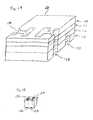
- FIG. 1Aprovides a perspective view of an exemplary temperature compensating device 10 comprising four integrated sheets 11 A, 11 B, 11 C and 11 D.
- Sheet 11 Acomprises a first sheet thermistor.
- Sheets 11 B and 11 Care ceramic sheets, and sheet 11 D comprises a second sheet thermistor.
- Conductively coated notches 13 A, 13 B, 13 C and 13 Dconveniently provide input, output and ground contacts.
- FIG. 2illustrates the first sheet thermistor 11 A.
- the sheet 11 Ais composed of thermistor material such as platinum-based negative temperature coefficient (NTC) thermistor material in a glass frit.
- the sheetis provided with conductively coated notches 13 A, 13 B and conductively filled holes 20 .
- a top conductive pattern and a bottom conductive patternform a pair of electrodes 12 A, 12 B separated by a region 21 of NTC material.
- the NTC material 21 between the two electrodesconstitutes an NTC thermistor serially connected between notches 13 A, 13 B.
- FIGS. 3A and 3Bshow the ceramic sheets 11 B and 11 C, respectively.
- Sheet 11 Bcan be a notched sheet of ceramic material.
- the notches 13 A and 13 Bare coated with conductive material to provide good electrical contact.
- the ceramicshould be an insulating ceramic with good thermal conductivity.
- FIG. 3Bshows a similar sheet that can be used for ceramic sheet 11 C.
- FIG. 4shows the second sheet thermistor 11 D.
- the sheetcan be composed of oxide-based positive temperature coefficient (PTC) thermistor material in a glass frit.
- the sheethas conductively coated notches 13 A, 13 B, 13 C and 13 D, conductively filled holes 20 and metallization patterns forming electrodes 42 A, 42 B, 42 C and 42 D. After firing, the regions of PTC material between the electrodes 42 A and ground electrode 42 C and between 42 B and 42 D form PTC thermistors to ground.
- PTCpositive temperature coefficient
- the device of FIG. 1is relatively easy to fabricate using the LTCC process.
- the sheet thermistors shown in FIGS. 2 and 4are fabricated by providing green sheets of thermistor material in a sinterable base such as a glass frit. Each green sheet is prepunched for holes 20 and notches 13 A, and conductive inks are applied to coat the notches, fill the holes and print the pattern for the electrodes.
- the green ceramic sheetsneed merely be notched and have the notches coated. The green sheets are then stacked and co-fired into an integral body.
- the thermistor materialcan be negative coefficient of temperature (“NTC”) material or positive coefficient of temperature (“PTC”) material.
- NTC thermistorsare typically based on oxides such as MgO or barium titanate; PTC thermistors are typically platinum-based.
- the ohmic value of each thermistor at a given temperatureis determined by the width of the electrodes (w), the thickness of the thermistor sheet (t), the gap (g) between the electrodes and the resistivity p of the material.
- the sheet thermistor device of FIGS. 1 - 4reduces air temperature modulation and thermal gradient problems since the thermistors are thicker, smaller in area and integral with ceramic layers. Because the thermistors are thicker, it is easier to define low ohmic value devices.
- An additional advantageis that the device provides an easy way to trim the resistance value of individual thermistors.
- the ohmic value of each thermistorcan be increased by reducing the amount of thermistor material between electrodes.
- the materialcan be removed by etching, laser trimming or abrasive trimming.
- An exemplary temperature compensating devicecan be constructed using the DuPont LTCC system 951, described in the DuPont material data sheet entitled “951 Low-Temperature Cofire Dielectric Tape”.
- the tapeis a mixture of organic binder and glass. When fired the tape forms the ceramic substrate for the circuit. Individual circuits are formed on a large wafer and then singulated after processing.
- a thermistor tapemay be formulated that is compatible with the 951 tape, but will include a metal-metal (platinum) conductor material with a positive TCR. Compatibility of TCE and sintering characteristics with the 951 tape is necessary to achieve the necessary part performance.
- a thermistor tapemay be formulated that is compatible with the 951 tape, but will include a metal oxide such as magnesium oxide conductor material with a negative TCR. Compatibility of TCE and sintering characteristics with the 951 tape is again necessary to achieve the necessary part performance.
- Prior to firing holes, or viasare punched in both the 951 and thermistor tapes. The holes correspond to the location of the thermistor electrodes.
- the active thermistoris formed between the rows of filled vias. After punching the vias are filled with DuPont 6141 silver conductor to form electrically conductive connections. Printing is accomplished using a squeegee printer and a metal stencil. After printing, the solvents in the material are dried at 70° C. for 30 minutes.
- Electrically conductive interconnectionsare then made by screen printing a metal ink such as DuPont 6142 silver. All conductor prints must be dried. After the via holes are filled and conductive traces are printed and dried the separate tape layers are aligned, stacked, and tacked together using a high temperature (200° C.), 3 mm diameter tool. The stacked tapes are then laminated at 3000-4000 PSI at 70° C. After lamination the assembly is heated to 400° C. to burn off the organic materials in the tape layers. After the burn-off stage the assembly is heated to 850° C. to sinter the glass. As the assembly exits the furnace and cools the circuit forms a solid ceramic mass. After firing individual circuits are separated from the wafer by dicing.
- a metal inksuch as DuPont 6142 silver. All conductor prints must be dried. After the via holes are filled and conductive traces are printed and dried the separate tape layers are aligned, stacked, and tacked together using a high temperature (200° C.), 3
Landscapes
- Engineering & Computer Science (AREA)
- Microelectronics & Electronic Packaging (AREA)
- Physics & Mathematics (AREA)
- Electromagnetism (AREA)
- Ceramic Engineering (AREA)
- Thermistors And Varistors (AREA)
Abstract
Description
- This invention relates to temperature compensating devices for compensating the effect of temperature changes in an electrical or electronic circuit. In particular, it relates to a temperature compensating device using integrated sheet thermistors for enhanced performance.[0001]
- Temperature compensating devices are important components in a wide variety of electrical and electronic circuits such as high frequency communication circuits. Communication circuits are typically constructed using components, such as semiconductor devices, whose properties change with temperature. For example, solid state amplifiers are made using semiconductor components, and the current carrying ability of these components decreases with increasing temperature, reducing the gain of the amplifier. In the absence of compensation, such temperature-induced changes can deteriorate the performance of the circuit.[0002]
- One method for compensating temperature-induced changes in a communication circuit is to cascade the circuit with a temperature compensating device whose pertinent characteristics vary oppositely with temperature. For example, an amplifier can be cascaded with a compensating device that increases in gain with increasing temperature. The cascaded combination minimizes gain variation with temperature.[0003]
- U.S. Pat. No. 5,332,981 issued to the present applicant and John Steponick on Jul. 26, 1994, and is incorporated herein by reference. The '981 patent, which is entitled “Temperature Variable Attenuator,” describes a passive temperature compensating device using at least two different thermistors which are deposited as films on a substrate. The temperature coefficients of the thermistors are different and are selected so that the attenuation changes at a controlled rate with temperature while the impedance remains substantially constant.[0004]
- Difficulties with the '981 device arise because the device relies on thermistors formed as thin, relatively large area films. The large area thin films are unduly susceptible to changes in air temperature. Moreover, there can be substantial temperature gradients across the thickness between the film/air interface and the film/substrate interface. As one consequence, forced air cooling, typically used for other systems components, can vary the thermistor temperature and produce unwanted gain ripple. Another difficulty is that the relatively large area of the film requires a relatively large substrate. This increases cost, consumes board space, and degrades high frequency performance. A third difficulty arising from the thin thermistor film is the difficulty in constructing the small size, low ohmic value thermistors required for low impedance circuits (50 Ω). The thin layers are highly resistive. Accordingly there is a need for improved temperature compensating circuits.[0005]
- In accordance with the invention, a temperature compensating device comprises one or more integrated sheet thermistors. Because the sheet thermistors are relatively thick and integral with the substrate, they are less susceptible to changes in air temperature and to temperature gradients. Moreover, the sheet thermistors can be made smaller in area, permitting more compact, less expensive devices that exhibit improved high frequency performance. The devices can advantageously be fabricated using the low temperature co-fired ceramic (LTCC) process.[0006]
- The advantages, nature and various additional features of the invention will appear more fully upon consideration of the illustrative embodiments now to be described in detail in connection with the accompanying drawings. In the drawings:[0007]
- FIGS. 1A and 1B are side and bottom perspective views of an exemplary temperature compensating device employing integral sheet thermistors;[0008]
- FIG. 2 is a transparent perspective view of a first sheet thermistor used in the device of FIG. 1;[0009]
- FIGS. 3A and 3B are views of ceramic sheets used in the device of FIG. 1;[0010]
- FIG. 4 is a transparent perspective view of a second sheet thermistor used in the device of FIG. 1; and[0011]
- FIG. 5 is a schematic circuit diagram of the device of FIG. 1.[0012]
- It is to be understood that the drawings are for illustrating the concepts of the invention and are not to scale.[0013]
- In essence, a temperature compensating device in accordance with the invention comprises an integrated structure composed of a plurality of sheet thermistors separated by ceramic sheets. A sheet is typically a layer having a thickness of about 0.001″ or more. Each sheet thermistor comprises a sheet composed of thermistor material having a pair of major surfaces that are preferably parallel. Electrodes laterally spaced apart on the major surfaces define one or more thermistors composed of the thermistor material in the region between the laterally spaced apart electrodes. The thermistors on different levels can be interconnected by metallized grooves or vias into any one of a variety of temperature compensating circuits.[0014]
- Referring to the drawings, FIG. 1A provides a perspective view of an exemplary[0015]
temperature compensating device 10 comprising four integrated sheets11A,11B,11C and11D. Sheet11A comprises a first sheet thermistor. Sheets11B and11C are ceramic sheets, and sheet11D comprises a second sheet thermistor. - Conductively coated[0016]
notches - The structure and operation of the device can be more clearly understood by consideration of the various constituent sheets. FIG. 2 illustrates the first sheet thermistor[0017]11A. The sheet11A is composed of thermistor material such as platinum-based negative temperature coefficient (NTC) thermistor material in a glass frit. The sheet is provided with conductively coated
notches holes 20. A top conductive pattern and a bottom conductive pattern, form a pair ofelectrodes region 21 of NTC material. TheNTC material 21 between the two electrodes constitutes an NTC thermistor serially connected betweennotches - FIGS. 3A and 3B show the ceramic sheets[0018]11B and11C, respectively. Sheet11B can be a notched sheet of ceramic material. The
notches - FIG. 4 shows the second sheet thermistor[0019]11D. The sheet can be composed of oxide-based positive temperature coefficient (PTC) thermistor material in a glass frit. The sheet has conductively
coated notches holes 20 and metallizationpatterns forming electrodes electrodes 42A and ground electrode42C and between42B and42D form PTC thermistors to ground. - It can be seen that the metallization patterns of FIGS. 2, 3,[0020]4 interconnect the sheet thermistors11A,11D into the π configuration temperature compensating circuit schematically shown in FIG. 5. Sheet11A corresponds to the NTC thermistor and sheet11D provides the two PTC thermistors connected to ground. The operation of this and other suitable temperature compensating circuits is described in the aforementioned U.S. Pat. No. 5,332,981 patent andReference Data for Engineers: Radio, Electronics, and Communications, Seventh Edition, Howard W. Sams & Co., Indianapolis, Ind., 1985, page 11-4.
- The device of FIG. 1 is relatively easy to fabricate using the LTCC process. In essence, the sheet thermistors shown in FIGS. 2 and 4 are fabricated by providing green sheets of thermistor material in a sinterable base such as a glass frit. Each green sheet is prepunched for[0021]
holes 20 andnotches 13A, and conductive inks are applied to coat the notches, fill the holes and print the pattern for the electrodes. The green ceramic sheets need merely be notched and have the notches coated. The green sheets are then stacked and co-fired into an integral body. - The thermistor material can be negative coefficient of temperature (“NTC”) material or positive coefficient of temperature (“PTC”) material. NTC thermistors are typically based on oxides such as MgO or barium titanate; PTC thermistors are typically platinum-based. The ohmic value of each thermistor at a given temperature is determined by the width of the electrodes (w), the thickness of the thermistor sheet (t), the gap (g) between the electrodes and the resistivity p of the material. The resistance R is given by R=ρg/tw. It will be appreciated that the metallization pattern can be configured to form any one of a variety of temperature compensating circuits.[0022]
- As compared with prior temperature compensating devices using thin film thermistors, the sheet thermistor device of FIGS.[0023]1-4 reduces air temperature modulation and thermal gradient problems since the thermistors are thicker, smaller in area and integral with ceramic layers. Because the thermistors are thicker, it is easier to define low ohmic value devices.
- An additional advantage is that the device provides an easy way to trim the resistance value of individual thermistors. The ohmic value of each thermistor can be increased by reducing the amount of thermistor material between electrodes. The material can be removed by etching, laser trimming or abrasive trimming.[0024]
- The invention can now be understood more clearly by consideration of the following specific embodiment.[0025]
- An exemplary temperature compensating device can be constructed using the DuPont LTCC system 951, described in the DuPont material data sheet entitled “951 Low-Temperature Cofire Dielectric Tape”. The tape is a mixture of organic binder and glass. When fired the tape forms the ceramic substrate for the circuit. Individual circuits are formed on a large wafer and then singulated after processing. A thermistor tape may be formulated that is compatible with the 951 tape, but will include a metal-metal (platinum) conductor material with a positive TCR. Compatibility of TCE and sintering characteristics with the 951 tape is necessary to achieve the necessary part performance. A thermistor tape may be formulated that is compatible with the 951 tape, but will include a metal oxide such as magnesium oxide conductor material with a negative TCR. Compatibility of TCE and sintering characteristics with the 951 tape is again necessary to achieve the necessary part performance. Prior to firing holes, or vias, are punched in both the 951 and thermistor tapes. The holes correspond to the location of the thermistor electrodes. The active thermistor is formed between the rows of filled vias. After punching the vias are filled with DuPont 6141 silver conductor to form electrically conductive connections. Printing is accomplished using a squeegee printer and a metal stencil. After printing, the solvents in the material are dried at 70° C. for 30 minutes. Electrically conductive interconnections are then made by screen printing a metal ink such as DuPont 6142 silver. All conductor prints must be dried. After the via holes are filled and conductive traces are printed and dried the separate tape layers are aligned, stacked, and tacked together using a high temperature (200° C.), 3 mm diameter tool. The stacked tapes are then laminated at 3000-4000 PSI at 70° C. After lamination the assembly is heated to 400° C. to burn off the organic materials in the tape layers. After the burn-off stage the assembly is heated to 850° C. to sinter the glass. As the assembly exits the furnace and cools the circuit forms a solid ceramic mass. After firing individual circuits are separated from the wafer by dicing.[0026]
- It is understood that the above-described embodiments are illustrative of only a few of the many possible specific embodiments, which can represent applications of the invention. Numerous and varied other arrangements can be made by those skilled in the art without departing from the spirit and scope of the invention.[0027]
Claims (9)
Priority Applications (4)
| Application Number | Priority Date | Filing Date | Title |
|---|---|---|---|
| US10/043,582US6759940B2 (en) | 2002-01-10 | 2002-01-10 | Temperature compensating device with integral sheet thermistors |
| AU2003209151AAU2003209151A1 (en) | 2002-01-10 | 2003-01-03 | Temperature compensation device with integral sheet thermistors |
| EP03707293AEP1470557A4 (en) | 2002-01-10 | 2003-01-03 | Temperature compensation device with integral sheet thermistors |
| PCT/US2003/000144WO2003060928A1 (en) | 2002-01-10 | 2003-01-03 | Temperature compensation device with integral sheet thermistors |
Applications Claiming Priority (1)
| Application Number | Priority Date | Filing Date | Title |
|---|---|---|---|
| US10/043,582US6759940B2 (en) | 2002-01-10 | 2002-01-10 | Temperature compensating device with integral sheet thermistors |
Publications (2)
| Publication Number | Publication Date |
|---|---|
| US20030128096A1true US20030128096A1 (en) | 2003-07-10 |
| US6759940B2 US6759940B2 (en) | 2004-07-06 |
Family
ID=21927901
Family Applications (1)
| Application Number | Title | Priority Date | Filing Date |
|---|---|---|---|
| US10/043,582Expired - LifetimeUS6759940B2 (en) | 2002-01-10 | 2002-01-10 | Temperature compensating device with integral sheet thermistors |
Country Status (4)
| Country | Link |
|---|---|
| US (1) | US6759940B2 (en) |
| EP (1) | EP1470557A4 (en) |
| AU (1) | AU2003209151A1 (en) |
| WO (1) | WO2003060928A1 (en) |
Cited By (58)
| Publication number | Priority date | Publication date | Assignee | Title |
|---|---|---|---|---|
| US20040094834A1 (en)* | 2002-11-19 | 2004-05-20 | Samsung Electro-Mechanics Co., Ltd. | Ceramic multilayer substrate and method for manufacturing the same |
| US20040099942A1 (en)* | 2002-11-25 | 2004-05-27 | Samsung Electro-Mechanics Co., Ltd. | Ceramic multilayer substrate and method for manufacturing the same |
| US20050041398A1 (en)* | 2002-05-01 | 2005-02-24 | Huemoeller Ronald Patrick | Integrated circuit substrate having embedded back-side access conductors and vias |
| WO2005098382A1 (en)* | 2004-04-05 | 2005-10-20 | E.G.O. Elektro-Gerätebau GmbH | Temperature sensor and method for adjusting said type of temperature sensor |
| WO2006114394A1 (en)* | 2005-04-25 | 2006-11-02 | Mettler-Toledo Ag | Thermoanalytic sensor |
| US7145238B1 (en) | 2004-05-05 | 2006-12-05 | Amkor Technology, Inc. | Semiconductor package and substrate having multi-level vias |
| US7185426B1 (en) | 2002-05-01 | 2007-03-06 | Amkor Technology, Inc. | Method of manufacturing a semiconductor package |
| US20080043447A1 (en)* | 2002-05-01 | 2008-02-21 | Amkor Technology, Inc. | Semiconductor package having laser-embedded terminals |
| US7334326B1 (en) | 2001-06-19 | 2008-02-26 | Amkor Technology, Inc. | Method for making an integrated circuit substrate having embedded passive components |
| US7501338B1 (en) | 2001-06-19 | 2009-03-10 | Amkor Technology, Inc. | Semiconductor package substrate fabrication method |
| US7548430B1 (en) | 2002-05-01 | 2009-06-16 | Amkor Technology, Inc. | Buildup dielectric and metallization process and semiconductor package |
| US7550857B1 (en) | 2006-11-16 | 2009-06-23 | Amkor Technology, Inc. | Stacked redistribution layer (RDL) die assembly package |
| US7589398B1 (en) | 2006-10-04 | 2009-09-15 | Amkor Technology, Inc. | Embedded metal features structure |
| US7633765B1 (en) | 2004-03-23 | 2009-12-15 | Amkor Technology, Inc. | Semiconductor package including a top-surface metal layer for implementing circuit features |
| US7670962B2 (en) | 2002-05-01 | 2010-03-02 | Amkor Technology, Inc. | Substrate having stiffener fabrication method |
| US7750250B1 (en) | 2006-12-22 | 2010-07-06 | Amkor Technology, Inc. | Blind via capture pad structure |
| US7752752B1 (en) | 2007-01-09 | 2010-07-13 | Amkor Technology, Inc. | Method of fabricating an embedded circuit pattern |
| US7960827B1 (en) | 2009-04-09 | 2011-06-14 | Amkor Technology, Inc. | Thermal via heat spreader package and method |
| US8222538B1 (en) | 2009-06-12 | 2012-07-17 | Amkor Technology, Inc. | Stackable via package and method |
| US8294276B1 (en) | 2010-05-27 | 2012-10-23 | Amkor Technology, Inc. | Semiconductor device and fabricating method thereof |
| US8300423B1 (en) | 2010-05-25 | 2012-10-30 | Amkor Technology, Inc. | Stackable treated via package and method |
| US8323771B1 (en) | 2007-08-15 | 2012-12-04 | Amkor Technology, Inc. | Straight conductor blind via capture pad structure and fabrication method |
| US8338229B1 (en) | 2010-07-30 | 2012-12-25 | Amkor Technology, Inc. | Stackable plasma cleaned via package and method |
| US8337657B1 (en) | 2010-10-27 | 2012-12-25 | Amkor Technology, Inc. | Mechanical tape separation package and method |
| US8471154B1 (en) | 2009-08-06 | 2013-06-25 | Amkor Technology, Inc. | Stackable variable height via package and method |
| US8482134B1 (en) | 2010-11-01 | 2013-07-09 | Amkor Technology, Inc. | Stackable package and method |
| US8525318B1 (en) | 2010-11-10 | 2013-09-03 | Amkor Technology, Inc. | Semiconductor device and fabricating method thereof |
| US8536462B1 (en) | 2010-01-22 | 2013-09-17 | Amkor Technology, Inc. | Flex circuit package and method |
| US8535961B1 (en) | 2010-12-09 | 2013-09-17 | Amkor Technology, Inc. | Light emitting diode (LED) package and method |
| US8557629B1 (en) | 2010-12-03 | 2013-10-15 | Amkor Technology, Inc. | Semiconductor device having overlapped via apertures |
| US8623753B1 (en) | 2009-05-28 | 2014-01-07 | Amkor Technology, Inc. | Stackable protruding via package and method |
| US8633598B1 (en) | 2011-09-20 | 2014-01-21 | Amkor Technology, Inc. | Underfill contacting stacking balls package fabrication method and structure |
| US8653674B1 (en) | 2011-09-15 | 2014-02-18 | Amkor Technology, Inc. | Electronic component package fabrication method and structure |
| US8717775B1 (en) | 2010-08-02 | 2014-05-06 | Amkor Technology, Inc. | Fingerprint sensor package and method |
| US8747591B1 (en)* | 2009-09-22 | 2014-06-10 | Sandia Corporation | Full tape thickness feature conductors for EMI structures |
| US8796561B1 (en) | 2009-10-05 | 2014-08-05 | Amkor Technology, Inc. | Fan out build up substrate stackable package and method |
| US8826531B1 (en) | 2005-04-05 | 2014-09-09 | Amkor Technology, Inc. | Method for making an integrated circuit substrate having laminated laser-embedded circuit layers |
| US8872329B1 (en) | 2009-01-09 | 2014-10-28 | Amkor Technology, Inc. | Extended landing pad substrate package structure and method |
| US8890329B2 (en) | 2011-04-26 | 2014-11-18 | Amkor Technology, Inc. | Semiconductor device |
| US8937381B1 (en) | 2009-12-03 | 2015-01-20 | Amkor Technology, Inc. | Thin stackable package and method |
| US20150055682A1 (en)* | 2012-03-30 | 2015-02-26 | Mitsubishi Materials Corporation | Film-type thermistor sensor |
| US9013011B1 (en) | 2011-03-11 | 2015-04-21 | Amkor Technology, Inc. | Stacked and staggered die MEMS package and method |
| US9029962B1 (en) | 2011-10-12 | 2015-05-12 | Amkor Technology, Inc. | Molded cavity substrate MEMS package fabrication method and structure |
| US9391043B2 (en) | 2012-11-20 | 2016-07-12 | Amkor Technology, Inc. | Semiconductor device and manufacturing method thereof |
| US9543242B1 (en) | 2013-01-29 | 2017-01-10 | Amkor Technology, Inc. | Semiconductor package and fabricating method thereof |
| US9691734B1 (en) | 2009-12-07 | 2017-06-27 | Amkor Technology, Inc. | Method of forming a plurality of electronic component packages |
| US9691635B1 (en) | 2002-05-01 | 2017-06-27 | Amkor Technology, Inc. | Buildup dielectric layer having metallization pattern semiconductor package fabrication method |
| US9704747B2 (en) | 2013-03-29 | 2017-07-11 | Amkor Technology, Inc. | Semiconductor device and manufacturing method thereof |
| US9704842B2 (en) | 2013-11-04 | 2017-07-11 | Amkor Technology, Inc. | Interposer, manufacturing method thereof, semiconductor package using the same, and method for fabricating the semiconductor package |
| US9721872B1 (en) | 2011-02-18 | 2017-08-01 | Amkor Technology, Inc. | Methods and structures for increasing the allowable die size in TMV packages |
| CN107084801A (en)* | 2017-06-27 | 2017-08-22 | 深圳市刷新智能电子有限公司 | The high-precision integrated form thermosensitive circuit and its manufacture method that can be responded rapidly to |
| CN107087357A (en)* | 2017-06-27 | 2017-08-22 | 深圳市刷新智能电子有限公司 | A kind of manufacture method of Temperature Humidity Sensor and Temperature Humidity Sensor |
| US9748154B1 (en) | 2010-11-04 | 2017-08-29 | Amkor Technology, Inc. | Wafer level fan out semiconductor device and manufacturing method thereof |
| CN107192470A (en)* | 2017-06-27 | 2017-09-22 | 深圳市刷新智能电子有限公司 | A kind of integrated form thermosensitive circuit and its manufacture method |
| US9960328B2 (en) | 2016-09-06 | 2018-05-01 | Amkor Technology, Inc. | Semiconductor device and manufacturing method thereof |
| TWI656330B (en)* | 2017-03-06 | 2019-04-11 | 日商Koa股份有限公司 | Temperature sensor component |
| US10811277B2 (en) | 2004-03-23 | 2020-10-20 | Amkor Technology, Inc. | Encapsulated semiconductor package |
| US11081370B2 (en) | 2004-03-23 | 2021-08-03 | Amkor Technology Singapore Holding Pte. Ltd. | Methods of manufacturing an encapsulated semiconductor device |
Families Citing this family (12)
| Publication number | Priority date | Publication date | Assignee | Title |
|---|---|---|---|---|
| WO2003096387A2 (en) | 2002-05-08 | 2003-11-20 | Phoseon Technology, Inc. | High efficiency solid-state light source and methods of use and manufacture |
| US7816638B2 (en) | 2004-03-30 | 2010-10-19 | Phoseon Technology, Inc. | LED array having array-based LED detectors |
| EP1866954B1 (en) | 2004-12-30 | 2016-04-20 | Phoseon Technology, Inc. | Methods and systems relating to light sources for use in industrial processes |
| US7829977B2 (en)* | 2007-11-15 | 2010-11-09 | Advanced Semiconductor Engineering, Inc. | Low temperature co-fired ceramics substrate and semiconductor package |
| KR101015843B1 (en) | 2009-10-29 | 2011-02-23 | 삼성모바일디스플레이주식회사 | Organic light emitting device |
| US20130021704A1 (en)* | 2011-07-20 | 2013-01-24 | Polytronics Technology Corp. | Over-current and over-temperature protection device |
| USD692896S1 (en)* | 2011-11-15 | 2013-11-05 | Connectblue Ab | Module |
| USD689053S1 (en)* | 2011-11-15 | 2013-09-03 | Connectblue Ab | Module |
| USD680119S1 (en)* | 2011-11-15 | 2013-04-16 | Connectblue Ab | Module |
| USD680545S1 (en)* | 2011-11-15 | 2013-04-23 | Connectblue Ab | Module |
| USD668658S1 (en)* | 2011-11-15 | 2012-10-09 | Connectblue Ab | Module |
| USD668659S1 (en)* | 2011-11-15 | 2012-10-09 | Connectblue Ab | Module |
Citations (7)
| Publication number | Priority date | Publication date | Assignee | Title |
|---|---|---|---|---|
| US5332981A (en)* | 1992-07-31 | 1994-07-26 | Emc Technology, Inc. | Temperature variable attenuator |
| US6284080B1 (en)* | 1997-02-21 | 2001-09-04 | Medtronic, Inc. | Barrier metallization in ceramic substrate for implantable medical devices |
| US6362723B1 (en)* | 1999-11-18 | 2002-03-26 | Murata Manufacturing Co., Ltd. | Chip thermistors |
| US6498068B1 (en)* | 1998-02-10 | 2002-12-24 | Murata Manufacturing Co., Ltd. | Methods of producing resistor elements |
| US6525395B1 (en)* | 1999-10-19 | 2003-02-25 | Murata Manufacturing Co., Ltd. | Chip-type composite electronic component and manufacturing method thereof |
| US6570477B2 (en)* | 2000-05-09 | 2003-05-27 | Innochips Technology | Low inductance multilayer chip and method for fabricating same |
| US6588094B2 (en)* | 1998-10-13 | 2003-07-08 | Murata Manufacturing Co., Ltd. | Method of producing thermistor chips |
Family Cites Families (15)
| Publication number | Priority date | Publication date | Assignee | Title |
|---|---|---|---|---|
| US3916264A (en)* | 1974-07-01 | 1975-10-28 | Texas Instruments Inc | Time delay apparatus |
| JPS57166474U (en)* | 1981-04-13 | 1982-10-20 | ||
| JP2798136B2 (en)* | 1987-09-07 | 1998-09-17 | 株式会社村田製作所 | Thermistor |
| DE4020383C2 (en)* | 1990-06-27 | 1999-04-01 | Bosch Gmbh Robert | Process for the protection of catalytic converters for exhaust gas purification and heat tone sensor for carrying out the process |
| EP0476657A1 (en)* | 1990-09-21 | 1992-03-25 | Siemens Aktiengesellschaft | Thermistor with negative temperature coefficient produced by multilayer technology |
| JP2833242B2 (en)* | 1991-03-12 | 1998-12-09 | 株式会社村田製作所 | NTC thermistor element |
| JP2689756B2 (en)* | 1991-04-19 | 1997-12-10 | 株式会社村田製作所 | Sudden change thermistor and manufacturing method thereof |
| JPH05243008A (en)* | 1992-03-03 | 1993-09-21 | Murata Mfg Co Ltd | Thermistor device |
| JPH06302404A (en)* | 1993-04-16 | 1994-10-28 | Murata Mfg Co Ltd | Lamination type positive temperature coefficient thermistor |
| US6020808A (en)* | 1997-09-03 | 2000-02-01 | Bourns Multifuse (Hong Kong) Ltd. | Multilayer conductive polymer positive temperature coefficent device |
| JPH11265804A (en)* | 1998-03-17 | 1999-09-28 | Murata Mfg Co Ltd | Ntc thermistor element |
| US6606023B2 (en)* | 1998-04-14 | 2003-08-12 | Tyco Electronics Corporation | Electrical devices |
| JP3402226B2 (en)* | 1998-11-19 | 2003-05-06 | 株式会社村田製作所 | Manufacturing method of chip thermistor |
| JP3736602B2 (en)* | 1999-04-01 | 2006-01-18 | 株式会社村田製作所 | Chip type thermistor |
| JP2001143904A (en)* | 1999-11-18 | 2001-05-25 | Matsushita Electric Ind Co Ltd | Composite laminated thermistor |
- 2002
- 2002-01-10USUS10/043,582patent/US6759940B2/ennot_activeExpired - Lifetime
- 2003
- 2003-01-03WOPCT/US2003/000144patent/WO2003060928A1/ennot_activeApplication Discontinuation
- 2003-01-03EPEP03707293Apatent/EP1470557A4/ennot_activeWithdrawn
- 2003-01-03AUAU2003209151Apatent/AU2003209151A1/ennot_activeAbandoned
Patent Citations (7)
| Publication number | Priority date | Publication date | Assignee | Title |
|---|---|---|---|---|
| US5332981A (en)* | 1992-07-31 | 1994-07-26 | Emc Technology, Inc. | Temperature variable attenuator |
| US6284080B1 (en)* | 1997-02-21 | 2001-09-04 | Medtronic, Inc. | Barrier metallization in ceramic substrate for implantable medical devices |
| US6498068B1 (en)* | 1998-02-10 | 2002-12-24 | Murata Manufacturing Co., Ltd. | Methods of producing resistor elements |
| US6588094B2 (en)* | 1998-10-13 | 2003-07-08 | Murata Manufacturing Co., Ltd. | Method of producing thermistor chips |
| US6525395B1 (en)* | 1999-10-19 | 2003-02-25 | Murata Manufacturing Co., Ltd. | Chip-type composite electronic component and manufacturing method thereof |
| US6362723B1 (en)* | 1999-11-18 | 2002-03-26 | Murata Manufacturing Co., Ltd. | Chip thermistors |
| US6570477B2 (en)* | 2000-05-09 | 2003-05-27 | Innochips Technology | Low inductance multilayer chip and method for fabricating same |
Cited By (120)
| Publication number | Priority date | Publication date | Assignee | Title |
|---|---|---|---|---|
| US7334326B1 (en) | 2001-06-19 | 2008-02-26 | Amkor Technology, Inc. | Method for making an integrated circuit substrate having embedded passive components |
| US7501338B1 (en) | 2001-06-19 | 2009-03-10 | Amkor Technology, Inc. | Semiconductor package substrate fabrication method |
| US7312103B1 (en) | 2002-05-01 | 2007-12-25 | Amkor Technology, Inc. | Method for making an integrated circuit substrate having laser-embedded conductive patterns |
| US7297562B1 (en) | 2002-05-01 | 2007-11-20 | Amkor Technology, Inc. | Circuit-on-foil process for manufacturing a laminated semiconductor package substrate having embedded conductive patterns |
| US7670962B2 (en) | 2002-05-01 | 2010-03-02 | Amkor Technology, Inc. | Substrate having stiffener fabrication method |
| US9691635B1 (en) | 2002-05-01 | 2017-06-27 | Amkor Technology, Inc. | Buildup dielectric layer having metallization pattern semiconductor package fabrication method |
| US8026587B1 (en) | 2002-05-01 | 2011-09-27 | Amkor Technology, Inc. | Semiconductor package including top-surface terminals for mounting another semiconductor package |
| US8110909B1 (en) | 2002-05-01 | 2012-02-07 | Amkor Technology, Inc. | Semiconductor package including top-surface terminals for mounting another semiconductor package |
| US7671457B1 (en) | 2002-05-01 | 2010-03-02 | Amkor Technology, Inc. | Semiconductor package including top-surface terminals for mounting another semiconductor package |
| US20050041398A1 (en)* | 2002-05-01 | 2005-02-24 | Huemoeller Ronald Patrick | Integrated circuit substrate having embedded back-side access conductors and vias |
| US20080043447A1 (en)* | 2002-05-01 | 2008-02-21 | Amkor Technology, Inc. | Semiconductor package having laser-embedded terminals |
| US8322030B1 (en)* | 2002-05-01 | 2012-12-04 | Amkor Technology, Inc. | Circuit-on-foil process for manufacturing a laminated semiconductor package substrate having embedded conductive patterns |
| US7548430B1 (en) | 2002-05-01 | 2009-06-16 | Amkor Technology, Inc. | Buildup dielectric and metallization process and semiconductor package |
| US7185426B1 (en) | 2002-05-01 | 2007-03-06 | Amkor Technology, Inc. | Method of manufacturing a semiconductor package |
| US9812386B1 (en) | 2002-05-01 | 2017-11-07 | Amkor Technology, Inc. | Encapsulated semiconductor package |
| US10461006B1 (en)* | 2002-05-01 | 2019-10-29 | Amkor Technology, Inc. | Encapsulated semiconductor package |
| US8341835B1 (en) | 2002-05-01 | 2013-01-01 | Amkor Technology, Inc. | Buildup dielectric layer having metallization pattern semiconductor package fabrication method |
| US7399661B2 (en) | 2002-05-01 | 2008-07-15 | Amkor Technology, Inc. | Method for making an integrated circuit substrate having embedded back-side access conductors and vias |
| US8316536B1 (en) | 2002-05-01 | 2012-11-27 | Amkor Technology, Inc. | Multi-level circuit substrate fabrication method |
| US20050098874A1 (en)* | 2002-11-18 | 2005-05-12 | Jun Seok T. | Ceramic multilayer substrate and method for manufacturing the same |
| US20040094834A1 (en)* | 2002-11-19 | 2004-05-20 | Samsung Electro-Mechanics Co., Ltd. | Ceramic multilayer substrate and method for manufacturing the same |
| US6965161B2 (en)* | 2002-11-19 | 2005-11-15 | Samsung Electro-Mechanics Co., Ltd. | Ceramic multilayer substrate and method for manufacturing the same |
| US20040099942A1 (en)* | 2002-11-25 | 2004-05-27 | Samsung Electro-Mechanics Co., Ltd. | Ceramic multilayer substrate and method for manufacturing the same |
| US6987315B2 (en) | 2002-11-25 | 2006-01-17 | Samsung Electro-Mechanics Co., Ltd. | Ceramic multilayer substrate |
| US20050168917A1 (en)* | 2002-11-25 | 2005-08-04 | Samsung Electro-Mechanics Co., Ltd. | Method for manufacturing ceramic multilayer substrate |
| US10811277B2 (en) | 2004-03-23 | 2020-10-20 | Amkor Technology, Inc. | Encapsulated semiconductor package |
| US7633765B1 (en) | 2004-03-23 | 2009-12-15 | Amkor Technology, Inc. | Semiconductor package including a top-surface metal layer for implementing circuit features |
| US11081370B2 (en) | 2004-03-23 | 2021-08-03 | Amkor Technology Singapore Holding Pte. Ltd. | Methods of manufacturing an encapsulated semiconductor device |
| US11094560B1 (en) | 2004-03-23 | 2021-08-17 | Amkor Technology Singapore Holding Pte. Ltd. | Encapsulated semiconductor package |
| US8227338B1 (en) | 2004-03-23 | 2012-07-24 | Amkor Technology, Inc. | Semiconductor package including a top-surface metal layer for implementing circuit features |
| US8018068B1 (en) | 2004-03-23 | 2011-09-13 | Amkor Technology, Inc. | Semiconductor package including a top-surface metal layer for implementing circuit features |
| WO2005098382A1 (en)* | 2004-04-05 | 2005-10-20 | E.G.O. Elektro-Gerätebau GmbH | Temperature sensor and method for adjusting said type of temperature sensor |
| US7365006B1 (en) | 2004-05-05 | 2008-04-29 | Amkor Technology, Inc. | Semiconductor package and substrate having multi-level vias fabrication method |
| US7145238B1 (en) | 2004-05-05 | 2006-12-05 | Amkor Technology, Inc. | Semiconductor package and substrate having multi-level vias |
| US8826531B1 (en) | 2005-04-05 | 2014-09-09 | Amkor Technology, Inc. | Method for making an integrated circuit substrate having laminated laser-embedded circuit layers |
| US7588367B2 (en) | 2005-04-25 | 2009-09-15 | Mettler-Toledo Ag | Thermoanalytical sensor |
| US20080080586A1 (en)* | 2005-04-25 | 2008-04-03 | Mettler-Toledo Ag | Thermoanalytical sensor |
| WO2006114394A1 (en)* | 2005-04-25 | 2006-11-02 | Mettler-Toledo Ag | Thermoanalytic sensor |
| US11848214B2 (en) | 2006-08-01 | 2023-12-19 | Amkor Technology Singapore Holding Pte. Ltd. | Encapsulated semiconductor package |
| US7589398B1 (en) | 2006-10-04 | 2009-09-15 | Amkor Technology, Inc. | Embedded metal features structure |
| US7911037B1 (en) | 2006-10-04 | 2011-03-22 | Amkor Technology, Inc. | Method and structure for creating embedded metal features |
| US8203203B1 (en) | 2006-11-16 | 2012-06-19 | Amkor Technology, Inc. | Stacked redistribution layer (RDL) die assembly package |
| US7550857B1 (en) | 2006-11-16 | 2009-06-23 | Amkor Technology, Inc. | Stacked redistribution layer (RDL) die assembly package |
| US7825520B1 (en) | 2006-11-16 | 2010-11-02 | Amkor Technology, Inc. | Stacked redistribution layer (RDL) die assembly package |
| US8629546B1 (en) | 2006-11-16 | 2014-01-14 | Amkor Technology, Inc. | Stacked redistribution layer (RDL) die assembly package |
| US8671565B1 (en) | 2006-12-22 | 2014-03-18 | Amkor Technology, Inc. | Blind via capture pad structure fabrication method |
| US7750250B1 (en) | 2006-12-22 | 2010-07-06 | Amkor Technology, Inc. | Blind via capture pad structure |
| US7752752B1 (en) | 2007-01-09 | 2010-07-13 | Amkor Technology, Inc. | Method of fabricating an embedded circuit pattern |
| US8323771B1 (en) | 2007-08-15 | 2012-12-04 | Amkor Technology, Inc. | Straight conductor blind via capture pad structure and fabrication method |
| US8872329B1 (en) | 2009-01-09 | 2014-10-28 | Amkor Technology, Inc. | Extended landing pad substrate package structure and method |
| US9462704B1 (en) | 2009-01-09 | 2016-10-04 | Amkor Technology, Inc. | Extended landing pad substrate package structure and method |
| US7960827B1 (en) | 2009-04-09 | 2011-06-14 | Amkor Technology, Inc. | Thermal via heat spreader package and method |
| US8623753B1 (en) | 2009-05-28 | 2014-01-07 | Amkor Technology, Inc. | Stackable protruding via package and method |
| US11089685B2 (en) | 2009-06-12 | 2021-08-10 | Amkor Technology Singapore Holding Pte. Ltd. | Stackable via package and method |
| US10206285B1 (en) | 2009-06-12 | 2019-02-12 | Amkor Technology, Inc. | Stackable via package and method |
| US8704368B1 (en) | 2009-06-12 | 2014-04-22 | Amkor Technology, Inc. | Stackable via package and method |
| US10034372B1 (en) | 2009-06-12 | 2018-07-24 | Amkor Technology, Inc. | Stackable via package and method |
| US10548221B1 (en) | 2009-06-12 | 2020-01-28 | Amkor Technology, Inc. | Stackable via package and method |
| US9012789B1 (en) | 2009-06-12 | 2015-04-21 | Amkor Technology, Inc. | Stackable via package and method |
| US11700692B2 (en) | 2009-06-12 | 2023-07-11 | Amkor Technology Singapore Holding Pte. Ltd. | Stackable via package and method |
| US9730327B1 (en) | 2009-06-12 | 2017-08-08 | Amkor Technology, Inc. | Stackable via package and method |
| US12035472B2 (en) | 2009-06-12 | 2024-07-09 | Amkor Technology Singapore Holding Ptd. Ltd. | Stackable via package and method |
| US8222538B1 (en) | 2009-06-12 | 2012-07-17 | Amkor Technology, Inc. | Stackable via package and method |
| US10257942B1 (en) | 2009-08-06 | 2019-04-09 | Amkor Technology, Inc. | Stackable variable height via package and method |
| US8471154B1 (en) | 2009-08-06 | 2013-06-25 | Amkor Technology, Inc. | Stackable variable height via package and method |
| US8747591B1 (en)* | 2009-09-22 | 2014-06-10 | Sandia Corporation | Full tape thickness feature conductors for EMI structures |
| US8796561B1 (en) | 2009-10-05 | 2014-08-05 | Amkor Technology, Inc. | Fan out build up substrate stackable package and method |
| US8937381B1 (en) | 2009-12-03 | 2015-01-20 | Amkor Technology, Inc. | Thin stackable package and method |
| US10546833B2 (en) | 2009-12-07 | 2020-01-28 | Amkor Technology, Inc. | Method of forming a plurality of electronic component packages |
| US9691734B1 (en) | 2009-12-07 | 2017-06-27 | Amkor Technology, Inc. | Method of forming a plurality of electronic component packages |
| US8536462B1 (en) | 2010-01-22 | 2013-09-17 | Amkor Technology, Inc. | Flex circuit package and method |
| US8300423B1 (en) | 2010-05-25 | 2012-10-30 | Amkor Technology, Inc. | Stackable treated via package and method |
| US8294276B1 (en) | 2010-05-27 | 2012-10-23 | Amkor Technology, Inc. | Semiconductor device and fabricating method thereof |
| US8338229B1 (en) | 2010-07-30 | 2012-12-25 | Amkor Technology, Inc. | Stackable plasma cleaned via package and method |
| US8717775B1 (en) | 2010-08-02 | 2014-05-06 | Amkor Technology, Inc. | Fingerprint sensor package and method |
| US8753730B1 (en) | 2010-10-27 | 2014-06-17 | Amkor Technology, Inc. | Mechanical tape separation package |
| US8337657B1 (en) | 2010-10-27 | 2012-12-25 | Amkor Technology, Inc. | Mechanical tape separation package and method |
| US9496210B1 (en) | 2010-11-01 | 2016-11-15 | Amkor Technology, Inc. | Stackable package and method |
| US12009343B1 (en) | 2010-11-01 | 2024-06-11 | Amkor Technology Singapore Holding Pte. Ltd. | Stackable package and method |
| US8482134B1 (en) | 2010-11-01 | 2013-07-09 | Amkor Technology, Inc. | Stackable package and method |
| US11855023B2 (en) | 2010-11-04 | 2023-12-26 | Amkor Technology Singapore Holding Pte. Ltd. | Wafer level fan out semiconductor device and manufacturing method thereof |
| US9748154B1 (en) | 2010-11-04 | 2017-08-29 | Amkor Technology, Inc. | Wafer level fan out semiconductor device and manufacturing method thereof |
| US10903181B2 (en) | 2010-11-04 | 2021-01-26 | Amkor Technology Singapore Holding Pte. Ltd. | Wafer level fan out semiconductor device and manufacturing method thereof |
| US8525318B1 (en) | 2010-11-10 | 2013-09-03 | Amkor Technology, Inc. | Semiconductor device and fabricating method thereof |
| US8557629B1 (en) | 2010-12-03 | 2013-10-15 | Amkor Technology, Inc. | Semiconductor device having overlapped via apertures |
| US9177932B1 (en) | 2010-12-03 | 2015-11-03 | Amkor Technology, Inc. | Semiconductor device having overlapped via apertures |
| US9837331B1 (en) | 2010-12-03 | 2017-12-05 | Amkor Technology, Inc. | Semiconductor device having overlapped via apertures |
| US8535961B1 (en) | 2010-12-09 | 2013-09-17 | Amkor Technology, Inc. | Light emitting diode (LED) package and method |
| US10347562B1 (en) | 2011-02-18 | 2019-07-09 | Amkor Technology, Inc. | Methods and structures for increasing the allowable die size in TMV packages |
| US9721872B1 (en) | 2011-02-18 | 2017-08-01 | Amkor Technology, Inc. | Methods and structures for increasing the allowable die size in TMV packages |
| US11488892B2 (en) | 2011-02-18 | 2022-11-01 | Amkor Technology Singapore Holding Pte. Ltd. | Methods and structures for increasing the allowable die size in TMV packages |
| US9013011B1 (en) | 2011-03-11 | 2015-04-21 | Amkor Technology, Inc. | Stacked and staggered die MEMS package and method |
| US8890329B2 (en) | 2011-04-26 | 2014-11-18 | Amkor Technology, Inc. | Semiconductor device |
| US8941250B1 (en) | 2011-09-15 | 2015-01-27 | Amkor Technology, Inc. | Electronic component package fabrication method and structure |
| US8653674B1 (en) | 2011-09-15 | 2014-02-18 | Amkor Technology, Inc. | Electronic component package fabrication method and structure |
| US8633598B1 (en) | 2011-09-20 | 2014-01-21 | Amkor Technology, Inc. | Underfill contacting stacking balls package fabrication method and structure |
| US8890337B1 (en) | 2011-09-20 | 2014-11-18 | Amkor Technology, Inc. | Column and stacking balls package fabrication method and structure |
| US9029962B1 (en) | 2011-10-12 | 2015-05-12 | Amkor Technology, Inc. | Molded cavity substrate MEMS package fabrication method and structure |
| US20150055682A1 (en)* | 2012-03-30 | 2015-02-26 | Mitsubishi Materials Corporation | Film-type thermistor sensor |
| US9728514B2 (en) | 2012-11-20 | 2017-08-08 | Amkor Technology, Inc. | Semiconductor device and manufacturing method thereof |
| US11527496B2 (en) | 2012-11-20 | 2022-12-13 | Amkor Technology Singapore Holding Pte. Ltd. | Semiconductor device comprising semiconductor die and interposer and manufacturing method thereof |
| US10679952B2 (en) | 2012-11-20 | 2020-06-09 | Amkor Technology, Inc. | Semiconductor device having an encapsulated front side and interposer and manufacturing method thereof |
| US9391043B2 (en) | 2012-11-20 | 2016-07-12 | Amkor Technology, Inc. | Semiconductor device and manufacturing method thereof |
| US9852976B2 (en) | 2013-01-29 | 2017-12-26 | Amkor Technology, Inc. | Semiconductor package and fabricating method thereof |
| US9543242B1 (en) | 2013-01-29 | 2017-01-10 | Amkor Technology, Inc. | Semiconductor package and fabricating method thereof |
| US9704747B2 (en) | 2013-03-29 | 2017-07-11 | Amkor Technology, Inc. | Semiconductor device and manufacturing method thereof |
| US9704842B2 (en) | 2013-11-04 | 2017-07-11 | Amkor Technology, Inc. | Interposer, manufacturing method thereof, semiconductor package using the same, and method for fabricating the semiconductor package |
| US11652038B2 (en) | 2013-11-19 | 2023-05-16 | Amkor Technology Singapore Holding Pte. Ltd. | Semiconductor package with front side and back side redistribution structures and fabricating method thereof |
| US12159823B2 (en) | 2013-11-19 | 2024-12-03 | Amkor Technology Singapore Holding Pte. Ltd. | Semiconductor package with front side and back side redistribution structures and fabricating method thereof |
| US10192816B2 (en) | 2013-11-19 | 2019-01-29 | Amkor Technology, Inc. | Semiconductor package and fabricating method thereof |
| US10943858B2 (en) | 2013-11-19 | 2021-03-09 | Amkor Technology Singapore Holding Pte. Ltd. | Semiconductor package and fabricating method thereof |
| US9960328B2 (en) | 2016-09-06 | 2018-05-01 | Amkor Technology, Inc. | Semiconductor device and manufacturing method thereof |
| US11437552B2 (en) | 2016-09-06 | 2022-09-06 | Amkor Technology Singapore Holding Pte. Ltd. | Semiconductor device with transmissive layer and manufacturing method thereof |
| US11942581B2 (en) | 2016-09-06 | 2024-03-26 | Amkor Technology Singapore Holding Pte. Ltd. | Semiconductor device with transmissive layer and manufacturing method thereof |
| US10784422B2 (en) | 2016-09-06 | 2020-09-22 | Amkor Technology, Inc. | Semiconductor device with optically-transmissive layer and manufacturing method thereof |
| US10490716B2 (en) | 2016-09-06 | 2019-11-26 | Amkor Technology, Inc. | Semiconductor device with optically-transmissive layer and manufacturing method thereof |
| TWI656330B (en)* | 2017-03-06 | 2019-04-11 | 日商Koa股份有限公司 | Temperature sensor component |
| CN107087357A (en)* | 2017-06-27 | 2017-08-22 | 深圳市刷新智能电子有限公司 | A kind of manufacture method of Temperature Humidity Sensor and Temperature Humidity Sensor |
| CN107084801A (en)* | 2017-06-27 | 2017-08-22 | 深圳市刷新智能电子有限公司 | The high-precision integrated form thermosensitive circuit and its manufacture method that can be responded rapidly to |
| CN107192470A (en)* | 2017-06-27 | 2017-09-22 | 深圳市刷新智能电子有限公司 | A kind of integrated form thermosensitive circuit and its manufacture method |
Also Published As
| Publication number | Publication date |
|---|---|
| AU2003209151A1 (en) | 2003-07-30 |
| WO2003060928A1 (en) | 2003-07-24 |
| EP1470557A1 (en) | 2004-10-27 |
| EP1470557A4 (en) | 2008-12-03 |
| US6759940B2 (en) | 2004-07-06 |
Similar Documents
| Publication | Publication Date | Title |
|---|---|---|
| US6759940B2 (en) | Temperature compensating device with integral sheet thermistors | |
| US4800459A (en) | Circuit substrate having ceramic multilayer structure containing chip-like electronic components | |
| US6720859B2 (en) | Temperature compensating device with embedded columnar thermistors | |
| Utsumi et al. | Monolithic multicomponents ceramic (MMC) substrate | |
| JP3019136B2 (en) | Thick film paste and ceramic circuit board using the same | |
| JP2001143904A (en) | Composite laminated thermistor | |
| JP3248377B2 (en) | Manufacturing method of multilayer ceramic wiring board | |
| JP3632592B2 (en) | Chip thermistor and manufacturing method thereof | |
| JP3250944B2 (en) | Wiring board | |
| JP3093602B2 (en) | Manufacturing method of ceramic circuit board | |
| JP2860862B2 (en) | Chip type CR network and manufacturing method thereof | |
| JPH05243008A (en) | Thermistor device | |
| JPH0547598A (en) | Cr array | |
| JPH07106811A (en) | High-frequency circuit | |
| JPH053161B2 (en) | ||
| EP0390944A1 (en) | Multilayer ceramic substrate and its manufacturing method | |
| JPH02271596A (en) | Manufacture of multilayered hybrid circuit | |
| JPH11204946A (en) | Ceramic circuit board with built-in components | |
| JP2001185447A (en) | Capacitor array | |
| JP2002111421A (en) | Noise filter | |
| JPH08339905A (en) | Thermistor and adjusting method thereof | |
| JP2001237107A (en) | Laminated chip thermistor | |
| JP2002043169A (en) | Multilayer ceramic capacitors | |
| JP2001210547A (en) | Capacitor array | |
| JP2001217515A (en) | Circuit board |
Legal Events
| Date | Code | Title | Description |
|---|---|---|---|
| AS | Assignment | Owner name:LAMINA CERAMICS, INC., NEW JERSEY Free format text:ASSIGNMENT OF ASSIGNORS INTEREST;ASSIGNOR:MAZZOCHETTE, JOSEPH;REEL/FRAME:014641/0090 Effective date:20040518 | |
| STCF | Information on status: patent grant | Free format text:PATENTED CASE | |
| AS | Assignment | Owner name:LAMINA LIGHTING, INC., NEW JERSEY Free format text:CHANGE OF NAME;ASSIGNOR:LAMINA CERAMICS, INC.;REEL/FRAME:019843/0536 Effective date:20060614 Owner name:LAMINA LIGHTING, INC.,NEW JERSEY Free format text:CHANGE OF NAME;ASSIGNOR:LAMINA CERAMICS, INC.;REEL/FRAME:019843/0536 Effective date:20060614 | |
| FPAY | Fee payment | Year of fee payment:4 | |
| AS | Assignment | Owner name:LIGHTING SCIENCE GROUP CORPORATION, FLORIDA Free format text:ASSIGNMENT OF ASSIGNORS INTEREST;ASSIGNORS:LAMINA LIGHTING, INC.;LLI ACQUISITION, INC.;REEL/FRAME:023141/0517 Effective date:20080729 Owner name:LIGHTING SCIENCE GROUP CORPORATION,FLORIDA Free format text:ASSIGNMENT OF ASSIGNORS INTEREST;ASSIGNORS:LAMINA LIGHTING, INC.;LLI ACQUISITION, INC.;REEL/FRAME:023141/0517 Effective date:20080729 | |
| AS | Assignment | Owner name:WELLS FARGO BANK, NATIONAL ASSOCIATION, FLORIDA Free format text:SECURITY AGREEMENT;ASSIGNOR:LIGHTING SCIENCE GROUP CORPORATION;REEL/FRAME:026109/0019 Effective date:20101122 | |
| AS | Assignment | Owner name:ARES CAPITAL CORPORATION, NEW YORK Free format text:SECURITY AGREEMENT;ASSIGNOR:LIGHTING SCIENCE GROUP CORPORATION;REEL/FRAME:026940/0875 Effective date:20110920 | |
| REMI | Maintenance fee reminder mailed | ||
| FPAY | Fee payment | Year of fee payment:8 | |
| SULP | Surcharge for late payment | Year of fee payment:7 | |
| AS | Assignment | Owner name:LIGHTING SCIENCE GROUP CORPORATION, FLORIDA Free format text:RELEASE BY SECURED PARTY;ASSIGNOR:WELLS FARGO BANK, NATIONAL ASSOCIATION;REEL/FRAME:032520/0074 Effective date:20140219 | |
| AS | Assignment | Owner name:LIGHTING SCIENCE GROUP CORPORATION, FLORIDA Free format text:RELEASE BY SECURED PARTY;ASSIGNOR:ARES CAPITAL CORPORATION;REEL/FRAME:032527/0427 Effective date:20140219 | |
| AS | Assignment | Owner name:FCC, LLC D/B/A FIRST CAPITAL, AS AGENT, GEORGIA Free format text:SECURITY INTEREST;ASSIGNORS:LIGHTING SCIENCE GROUP CORPORATION;BIOLOGICAL ILLUMINATION, LLC;REEL/FRAME:032765/0910 Effective date:20140425 | |
| AS | Assignment | Owner name:MEDLEY CAPTIAL CORPORATION, AS AGENT, NEW YORK Free format text:SECURITY INTEREST;ASSIGNORS:LIGHTING SCIENCE GROUP CORPORATION;BIOLOGICAL ILLUMINATION, LLC;REEL/FRAME:033072/0395 Effective date:20140219 | |
| AS | Assignment | Owner name:ACF FINCO I LP, NEW YORK Free format text:ASSIGNMENT AND ASSUMPTION OF SECURITY INTERESTS IN PATENTS;ASSIGNOR:FCC, LLC D/B/A FIRST CAPITAL;REEL/FRAME:035774/0632 Effective date:20150518 | |
| FPAY | Fee payment | Year of fee payment:12 | |
| SULP | Surcharge for late payment | Year of fee payment:11 | |
| AS | Assignment | Owner name:BIOLOGICAL ILLUMINATION, LLC, A DELAWARE LIMITED L Free format text:RELEASE BY SECURED PARTY;ASSIGNOR:ACF FINCO I LP, A DELAWARE LIMITED PARTNERSHIP;REEL/FRAME:042340/0471 Effective date:20170425 Owner name:LIGHTING SCIENCE GROUP CORPORATION, A DELAWARE COR Free format text:RELEASE BY SECURED PARTY;ASSIGNOR:ACF FINCO I LP, A DELAWARE LIMITED PARTNERSHIP;REEL/FRAME:042340/0471 Effective date:20170425 | |
| AS | Assignment | Owner name:BIOLOGICAL ILLUMINATION, LLC, A DELAWARE LIMITED L Free format text:RELEASE BY SECURED PARTY;ASSIGNOR:MEDLEY CAPITAL CORPORATION;REEL/FRAME:048018/0515 Effective date:20180809 Owner name:LIGHTING SCIENCE GROUP CORPORATION, A DELAWARE COR Free format text:RELEASE BY SECURED PARTY;ASSIGNOR:MEDLEY CAPITAL CORPORATION;REEL/FRAME:048018/0515 Effective date:20180809 |