US20030127654A1 - Semiconductor component which emits radiation, and method for producing the same - Google Patents
Semiconductor component which emits radiation, and method for producing the sameDownload PDFInfo
- Publication number
- US20030127654A1 US20030127654A1US10/203,728US20372802AUS2003127654A1US 20030127654 A1US20030127654 A1US 20030127654A1US 20372802 AUS20372802 AUS 20372802AUS 2003127654 A1US2003127654 A1US 2003127654A1
- Authority
- US
- United States
- Prior art keywords
- radiation
- fact
- semiconductor component
- window
- pursuant
- Prior art date
- Legal status (The legal status is an assumption and is not a legal conclusion. Google has not performed a legal analysis and makes no representation as to the accuracy of the status listed.)
- Granted
Links
Images


Classifications
- H—ELECTRICITY
- H10—SEMICONDUCTOR DEVICES; ELECTRIC SOLID-STATE DEVICES NOT OTHERWISE PROVIDED FOR
- H10H—INORGANIC LIGHT-EMITTING SEMICONDUCTOR DEVICES HAVING POTENTIAL BARRIERS
- H10H20/00—Individual inorganic light-emitting semiconductor devices having potential barriers, e.g. light-emitting diodes [LED]
- H10H20/80—Constructional details
- H10H20/83—Electrodes
- H10H20/832—Electrodes characterised by their material
- H—ELECTRICITY
- H01—ELECTRIC ELEMENTS
- H01L—SEMICONDUCTOR DEVICES NOT COVERED BY CLASS H10
- H01L21/00—Processes or apparatus adapted for the manufacture or treatment of semiconductor or solid state devices or of parts thereof
- H01L21/02—Manufacture or treatment of semiconductor devices or of parts thereof
- H01L21/04—Manufacture or treatment of semiconductor devices or of parts thereof the devices having potential barriers, e.g. a PN junction, depletion layer or carrier concentration layer
- H01L21/18—Manufacture or treatment of semiconductor devices or of parts thereof the devices having potential barriers, e.g. a PN junction, depletion layer or carrier concentration layer the devices having semiconductor bodies comprising elements of Group IV of the Periodic Table or AIIIBV compounds with or without impurities, e.g. doping materials
- H01L21/30—Treatment of semiconductor bodies using processes or apparatus not provided for in groups H01L21/20 - H01L21/26
- H01L21/31—Treatment of semiconductor bodies using processes or apparatus not provided for in groups H01L21/20 - H01L21/26 to form insulating layers thereon, e.g. for masking or by using photolithographic techniques; After treatment of these layers; Selection of materials for these layers
- H01L21/3205—Deposition of non-insulating-, e.g. conductive- or resistive-, layers on insulating layers; After-treatment of these layers
- H01L21/321—After treatment
- H01L21/3213—Physical or chemical etching of the layers, e.g. to produce a patterned layer from a pre-deposited extensive layer
- H01L21/32139—Physical or chemical etching of the layers, e.g. to produce a patterned layer from a pre-deposited extensive layer using masks
- H—ELECTRICITY
- H10—SEMICONDUCTOR DEVICES; ELECTRIC SOLID-STATE DEVICES NOT OTHERWISE PROVIDED FOR
- H10H—INORGANIC LIGHT-EMITTING SEMICONDUCTOR DEVICES HAVING POTENTIAL BARRIERS
- H10H20/00—Individual inorganic light-emitting semiconductor devices having potential barriers, e.g. light-emitting diodes [LED]
- H10H20/01—Manufacture or treatment
- H10H20/011—Manufacture or treatment of bodies, e.g. forming semiconductor layers
- H10H20/018—Bonding of wafers
- H—ELECTRICITY
- H10—SEMICONDUCTOR DEVICES; ELECTRIC SOLID-STATE DEVICES NOT OTHERWISE PROVIDED FOR
- H10H—INORGANIC LIGHT-EMITTING SEMICONDUCTOR DEVICES HAVING POTENTIAL BARRIERS
- H10H20/00—Individual inorganic light-emitting semiconductor devices having potential barriers, e.g. light-emitting diodes [LED]
- H10H20/80—Constructional details
- H10H20/81—Bodies
- H10H20/819—Bodies characterised by their shape, e.g. curved or truncated substrates
- H—ELECTRICITY
- H10—SEMICONDUCTOR DEVICES; ELECTRIC SOLID-STATE DEVICES NOT OTHERWISE PROVIDED FOR
- H10H—INORGANIC LIGHT-EMITTING SEMICONDUCTOR DEVICES HAVING POTENTIAL BARRIERS
- H10H20/00—Individual inorganic light-emitting semiconductor devices having potential barriers, e.g. light-emitting diodes [LED]
- H10H20/80—Constructional details
- H10H20/83—Electrodes
- H10H20/831—Electrodes characterised by their shape
- H10H20/8312—Electrodes characterised by their shape extending at least partially through the bodies
- H—ELECTRICITY
- H10—SEMICONDUCTOR DEVICES; ELECTRIC SOLID-STATE DEVICES NOT OTHERWISE PROVIDED FOR
- H10H—INORGANIC LIGHT-EMITTING SEMICONDUCTOR DEVICES HAVING POTENTIAL BARRIERS
- H10H20/00—Individual inorganic light-emitting semiconductor devices having potential barriers, e.g. light-emitting diodes [LED]
- H10H20/80—Constructional details
- H10H20/83—Electrodes
- H10H20/832—Electrodes characterised by their material
- H10H20/833—Transparent materials
- H—ELECTRICITY
- H10—SEMICONDUCTOR DEVICES; ELECTRIC SOLID-STATE DEVICES NOT OTHERWISE PROVIDED FOR
- H10H—INORGANIC LIGHT-EMITTING SEMICONDUCTOR DEVICES HAVING POTENTIAL BARRIERS
- H10H20/00—Individual inorganic light-emitting semiconductor devices having potential barriers, e.g. light-emitting diodes [LED]
- H10H20/80—Constructional details
- H10H20/81—Bodies
- H10H20/822—Materials of the light-emitting regions
- H10H20/824—Materials of the light-emitting regions comprising only Group III-V materials, e.g. GaP
- H10H20/825—Materials of the light-emitting regions comprising only Group III-V materials, e.g. GaP containing nitrogen, e.g. GaN
- H—ELECTRICITY
- H10—SEMICONDUCTOR DEVICES; ELECTRIC SOLID-STATE DEVICES NOT OTHERWISE PROVIDED FOR
- H10H—INORGANIC LIGHT-EMITTING SEMICONDUCTOR DEVICES HAVING POTENTIAL BARRIERS
- H10H20/00—Individual inorganic light-emitting semiconductor devices having potential barriers, e.g. light-emitting diodes [LED]
- H10H20/80—Constructional details
- H10H20/84—Coatings, e.g. passivation layers or antireflective coatings
- H10H20/841—Reflective coatings, e.g. dielectric Bragg reflectors
Definitions
- This inventionrelates to a radiation-emitting semiconductor component pursuant to the preamble of Patent claims 1, 5, 8, and 42, and a method for manufacturing it pursuant to the preamble of Patent claim 34.
- the inventionrelates in particular to a radiation-emitting semiconductor component with a nitride-based active multilayered structure applied to a silicon carbide-based epitaxial substrate.
- Radiation-emitting semiconductor components of the kind mentionedusually have a semiconductor multilayered structure with an active radiation-generating layer that is applied to a carrier transparent to radiation. The radiation is output through the carrier. In this arrangement, however, the radiation yield is sharply reduced by total reflection of the produced radiation at the carrier surface.
- the fraction of totally reflected radiation that cannot be outputis especially high because of the orthogonal arrangement of lateral faces and principal faces of the carrier.
- the radiation yieldcan be increased by forming recesses in the carrier whose lateral faces are preferably inclined relative to the principal faces of the carrier.
- a form such as that specified in the priority-determining Patent Application DE 100 067 38.7is especially beneficial.
- the contents of this Patent Applicationare explicitly incorporated in the contents of the present Patent Application.
- a corresponding componentis shown schematically in FIG. 17.
- the semiconductor component shownhas a window 151 transparent to radiation, to which is applied a radiation-producing multilayered structure 152 .
- At least one lateral face of the window 151is configured so that a first subregion 154 is inclined, concave, or stepped relative to the normal to the multilayered structure 152 , which is adjoined by a second region 155 positioned parallel to the normal to the multilayered structure.
- the inventionproceeds from the assumption that the ratio of output radiation power to the electrical power to be supplied for it is critical for the degree of efficiency.
- the optical output powerdepends on the degree of output, along with the current flowing through the component.
- the degree of outputindicates how large is the fraction of output radiation relative to the total radiation produced.
- the electrical poweris determined by the current flowing and the series resistance of the component. The degree of efficiency can therefore be increased in particular by lowering the series resistance and by increasing the degree of output.
- a first form of embodimentprovides for forming a radiation-emitting semiconductor component with a multilayered structure, an active layer that generates radiation within the multilayered structure, and a window transparent to radiation with a first principal face and a second principal face opposite the first principal face, with at least one recess being formed in the window to constitute inclined radiation output faces, and at least one lateral surface of the window and/or of the recess being provided with a contact surface.
- the contact surfacepreferably also extends over the second principal face of the window or subregions thereof.
- the current path from the contact surface to the active layeris shortened on the average by this arrangement of the contact surface, and thus beneficially reduces the series resistance of the component.
- the recess in the inventionserves to increase the radiation yield. Either direct output or reflection in a direction favoring output is produced in particular by lateral faces that are inclined relative to the principal faces of the window.
- a recess in the windowmeans both an indentation in the second principal face of the window or removal of material from an edge of the window, as shown for example in FIG. 15. When material is removed from the edge, the lateral surfaces of the window and of the recess partially coincide.
- a second contact surface on the multilayered structureis preferably provided for in the invention. This provides for current being fed in close to the active layer within the multilayered structure. It is especially advantageous for this contact surface to be largely transparent to radiation, so that radiation output is also possible through the second contact surface. This can be achieved, for example, by appropriately thin metallization or suitable transparent, electrically conductive films.
- the first contact surfaceis a reflector. Because of this, the portions of the radiation that strike the contact surface from inside the window are not absorbed, but are reflected back, so that subsequent output is possible. Thus a contact surface that is transparent to radiation and one that is reflective contribute to increasing the radiation yield, since they assist the output of radiation either directly or indirectly.
- a second embodiment of the inventionprovides forming a radiation-emitting semiconductor component with a multilayered structure, an active layer within the multilayered structure serving to generate radiation, and a window transparent to radiation, with a first principal face and a second principal face opposite the first principal face, with at least one recess being formed in the window to form an inclined radiation output surface.
- the componenthere has at least one contact surface with a plurality of openings.
- At least one of the window surfacesis provided, at least in part, with a first contact surface and for the multilayered structure to be provided, at least in part, with a second contact surface, with at least one of the contact surfaces having a plurality of openings.
- perforated contact surfaceshave the advantage over thin contact surfaces transparent to radiation, of higher long-term stability, particularly in a casting composition, for example such as epoxy resin.
- These perforated contact surfacescan also be made so that they have high transmission in the area of the openings and high reflection in the areas coated with contact material, so that absorption and therefore radiation loss is slight on these contact surfaces.
- Perforated contact surfaces on the multilayered structurealso have the advantage that they do not seal off the multilayered structure, so that for example gases such as hydrogen that reach the multilayered structure during manufacture can diffuse out of it. This also reduces the risk of such gases aggregating at the interface between the multilayered structure and the contact surface, passivating the contact surface, and thus increasing contact resistance and series resistance.
- the openings in the contact surface(s)are preferably circular, square, rectangular, hexagonal, or in the shape of crossed slits. These forms are especially suitable for a regular arrangement and are comparatively easy to make technically.
- the openingsare preferably packed tightly provided that the intermediate areas of the contact surfaces form a continuous network and the width of the areas meet the requirements for current input into the component.
- the shapes mentioneddo not constitute a limitation of the invention thereto.
- the recessis made in the form of an indentation in the second principal face of the window. It is beneficial that no change of the basic window enveloping shape is necessary, so that in particular production systems, which are often designed for a given basic window shape, can continue to be used without change. A plurality of indentations can also be made in the second principal face, whereby the radiation yield is further increased.
- This configurationis advantageous especially for large-area semiconductor components, since the ratio of area to circumference rises with increasing chip area, and thus more indentations can be placed in the surface than circumferentially.
- the indentation in the second principal faceis designed with a triangular, trapezoidal, or semicircular cross section (section perpendicular to the second principal face).
- the cross sectioncan also have the shape of a rectangle with added triangle, trapezoid, or semicircle.
- the formation of recesses with at least one lateral face not in an orthogonal position to the principal facesis advantageous.
- the angle of incidence of the radiation produced relative to the normal to the lateral faces, and thus the fraction of totally reflected radiationis thereby lowered, or reflection toward the flanks of the window is brought about, so that direct output or at least output after further reflections can take place.
- the latterapplies in particular to the lateral faces of the indentation that are provided with a reflective contact surface.
- the indentation in the second principal face of the windowis preferably in the form of a trough with one of the aforementioned cross-sectional shapes.
- Such an indentationcan be made, for example, by sawing into the window from the second principal face and using a saw blade with shaped rim. If this sawing is performed in the wafer composite, then a plurality of windows can advantageously be structured in one production step.
- the indentationscan also be etched in place.
- spatially isolated indentation shapes bordered all aroundcan be formed. The structuring of a plurality of windows in the wafer composite in one production step is also advantageously possible here.
- the recess that increases radiation yieldis formed at the edge of the second principal face and is so shaped that the window is tapered down toward the second principal face. It is preferred for the recess to be made so that the lateral faces of the recess have a first subregion inclined relative to the normal to the multilayered structure in the vicinity of the multilayered structure, that changes at greater distance from the multilayered structure to a second subregion running parallel to the normal to the multilayered structure.
- the windowis preferably formed as a parallelepiped in the section corresponding to the second region. It is advantageous that the radiation yield is increased by the inclined subregion, while the remaining area of the window has a square basic shape and thus can easily be mounted.
- the lateral faces [of] the second subregionare provided with a contact surface. The contact surface can also extend over the first subregion of the lateral faces, and can then preferably be made reflective, so that the radiation yield toward the multilayered structure is increased by reflection of the radiation produced.
- the described structurecan be formed advantageously at low production cost, for example by sawing a wafer with a saw blade with shaped edge to isolate the semiconductor bodies, and then singling the semiconductor bodies by breaking the wafer. Prior sawing of the wafer is desirable to facilitate singling by breaking.
- the described window shapecan be excavated at the same time by using a suitable saw blade with shaped edge.
- Other advantageous configurations in this regardare specified in DE 100 067 38.7, to which this invention refers in particular.
- a manufacturing method pursuant to the inventionbegins with preparation of a window layer, from which the actual window will later be produced.
- a semiconductor layer sequence corresponding to the multilayered structureis applied to the window layer. It is preferably applied epitaxially or in the context of a wafer-bonding procedure.
- the window layerat the same time advantageously represents the epitaxy substrate.
- the semiconductor layer sequenceis produced first on a suitable substrate, and is then bonded to the window layer. Materials that are unsuitable for an epitaxial process can also advantageously be used here as window material.
- the window layeris structured to develop the recess in a suitable manner. Structuring can be accomplished, for example as described, by sawing or etching the window layer. Structuring can also be performed in multiple steps, not necessarily in succession. Thus, with regard to the mechanical breakage stability of the window layer, it is advantageous to first prestructure the window layer and to perform the final structuring only at a later stage of the production process.
- the contact surfacesare applied to the window layer.
- the contact surfacesare preferably vapor-deposited or sputtered on for contact metallization.
- the semiconductor componentsare completed. This includes in particular the singling of the composite of window layer and semiconductor layer sequence into a plurality of windows with multilayered structure located thereon. The singling is performed preferably by sawing and/or breaking the window layer. Additional contact surfaces, for example contact metallizations, can also be applied to the multilayered structure in the course of completion.
- vapor deposition systemsare ordinarily used, from which the metal vapor originates with a given preferential direction. It is advantageous in this case to arrange the surface of the window layer to be subjected to vapor deposition at an angle to this preferential direction. In this way, deposition of the metal vapor on the second principal face of the window layer and also on the lateral faces of the recesses formed by the structuring is achieved.
- the semiconductor layer sequenceis first applied to the window layer, the window layer is then structured, and finally it is subjected to vapor deposition to develop the contact surfaces.
- existing production equipmentcan be used for this without changes, since with epitaxy the window layer does not yet differ from window layers pursuant to the state of the art.
- the window layeris structured only at the end of the manufacturing process, so that the risk of breakage of the window layer in the preceding steps is comparatively slight.
- a process in which the window layer is first structured and provided with contact surfacesrepresents a second advantageous alternative.
- the semiconductor layer sequenceis then applied.
- higher temperaturessuch as those necessary for sintering certain contact metallizations can be used to perform the contact metallization. These temperatures are usually so high that the semiconductor layer sequence would be damaged by them. Therefore, such damage is avoided by performing the contact metallization at the beginning of the manufacturing process.
- the structuring of the window layertakes place in two steps.
- the window layeris first prestructured to the extent necessary for developing the contact surfaces on the lateral faces.
- the contact surfacesare then developed, for example by vapor deposition.
- the semiconductor layer sequenceis then applied to the window layer prestructured in this way and provided with contact surfaces.
- the window layeris then subjected to final structuring.
- This second structuring stepis preferably combined with isolation of the components, for example by sawing the window layer with a shaped saw blade, and then breaking it apart.
- the window layercan also be mounted on a suitable auxiliary support.
- FIG. 1a schematic cross sectional illustration of a first example of embodiment of a semiconductor component pursuant to the invention
- FIG. 2a schematic cross sectional illustration of a second example of embodiment of a semiconductor component pursuant to the invention
- FIG. 3a schematic cross sectional illustration of a third example of embodiment of a semiconductor component pursuant to the invention
- FIG. 4a schematic cross sectional illustration of a fourth example of embodiment of a semiconductor component pursuant to the invention
- FIG. 5a schematic cross sectional illustration of a fifth example of embodiment of a semiconductor component pursuant to the invention
- FIG. 6a schematic cross sectional illustration of a sixth example of embodiment of a semiconductor component pursuant to the invention
- FIG. 7a schematic cross sectional illustration of a seventh example of embodiment of a semiconductor component pursuant to the invention
- FIG. 8a schematic cross sectional illustration of an eighth example of embodiment of a semiconductor component pursuant to the invention
- FIG. 9a schematic cross sectional illustration of a ninth example of embodiment of a semiconductor component pursuant to the invention.
- FIG. 10a schematic cross sectional illustration of a tenth example of embodiment of a semiconductor component pursuant to the invention
- FIG. 11a schematic cross sectional illustration of an eleventh example of embodiment of a semiconductor component pursuant to the invention
- FIG. 12a schematic perspective illustration of a twelfth example of embodiment of a semiconductor component pursuant to the invention
- FIG. 13a schematic illustration of a thirteenth example of embodiment of a semiconductor component pursuant to the invention
- FIG. 14a schematic illustration of a first example of embodiment of a manufacturing process pursuant to the invention in five intermediate steps
- FIG. 15a schematic illustration of a second example of embodiment of a manufacturing process pursuant to the invention in six intermediate steps
- FIG. 16a device for implementing an intermediate step in the examples of embodiment of a manufacturing process pursuant to the invention
- FIG. 17a schematic illustration of a radiation-emitting semiconductor component pursuant to the priority-determining Patent Application DE 100 067 38.7.
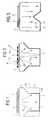
- FIG. 1The example of embodiment shown in FIG. 1 has a window 1 with a first principal face 2 and a second principal face 3 .
- a multilayered structure 4 with an active layer 5 that emits radiation during operationis applied to the first principal face 2 and is coated with a contact metallization 6 .
- the window 1itself is formed from a cuboid base form 7 rectangular in cross section that has recesses 8 on its circumference.
- the window flanks 10thus produced also correspond to the lateral faces of the recess and have a first subregion 10 a that is arranged at an angle to the principal faces 2 , 3 of the window and that changes into a second subregion 10 b orthogonal to the principal faces at a greater distance from the multilayered structure 4 .
- the window flanksare provided with contact metallization 11 that also covers the second principal face 3 of the window 1 .
- the current paths 12 from the active layer to the contact surface 11are shortened on the average by the contact surface 11 raised on the window flank 10 b, and thus the series resistance of the component is advantageously lowered.
- the radiationis preferably output in the inclined region 10 a of the window flanks.
- the contact metallization 11extends over the inclined subregions 10 a of the window flanks. This achieves a further shortening of the current paths 12 and thus a reduction of series resistance. Of course the subregions 10 a are then no longer available for direct radiation output. In this example of embodiment, therefore, the contact metallization 11 is made reflective so that the fractions of radiation emitted into the window for the most part are again reflected toward the multilayered structure 4 and are subsequently output. This is made clear by way of example by the beams 13 a and 13 b. Alternatively, the corresponding contact surfaces can also be perforated.
- the recess 8runs through the center of the second principal face 3 as a central indentation.
- the contact metallization 11is developed over the entire area over the second principal face 3 and the lateral faces of the indentation 8 .
- the current path 12 to the active layeris shortened in this way within the indentation 8 , and the series resistance of the component is reduced.
- the contact metallizationcan again be made reflective to increase the radiation yield.
- FIG. 4shows a fourth example of embodiment, in which the envelope of the first example of embodiment is advantageously combined with the central indentation of the third example of embodiment.
- the series resistanceis advantageously lowered by the shortening of the current path 12 as in the third example of embodiment, with the window flank being available at the same time for output of radiation.
- the radiation yieldis increased by the radiation fractions 13 reflected out laterally.
- the contact metallization 11extends both across the central indentation 8 in the second principal face of the window 1 and across subregions of the window flanks 10 .
- the series resistanceis lowered further in this way, with this entailing a reduced radiation yield in the area of the contact metallization.
- the fourth or the fifth example of embodimentmay be more advantageous, with the transition between these two examples of embodiment being continuous depending on the extent of the contact metallization on the window flanks.
- the radiation yieldcan be increased by reflection at the central indentation 8 in the second principal face 3 in various ways.
- One possibilityhas already been shown in the context of the fourth example of embodiment in FIG. 4, beam 13 c. If the angle of opening of the central indentation 8 is enlarged, the result is to increase reflection toward the multilayered structure 4 and thus output through the multilayered structure 4 .
- FIG. 6This is illustrated in the sixth example of embodiment in FIG. 6 with reference to the beam 13 d.
- this example of embodimentcorresponds to the fourth example of embodiment, FIG. 4.
- the central indentation 8is cut distinctly deeper than in FIG. 4 and has a five-cornered cross section, which is composed of a rectangle with added triangle.
- the angle of opening of the triangleis greater than shown in the example of embodiment illustrated in FIG. 4 and causes increased reflection toward the multilayered structure 4 . It is advantageous in this case to perforate the contact surface 6 on the multilayered structure and thus enlarge the output through this contact surface.
- the deeply cut and completely metallized recess 8also leads to an especially great shortening of the current path 12 because of the closeness of the bottom face of the recess to the multilayered structure 4 .
- the angle of opening of the central recessis chosen to be smaller. This leads to increased reflection toward the inclined lateral window face sections 10 a , and in connection with this to increased output on the part of the multilayered structure 4 . It is also advantageous here to perforate the contact surface 6 on the multilayered structure 4 .
- Various beam pathsare shown schematically by the beams 13 .
- the second principal face 3 and the multilayered structure 4are provided with contact surfaces, with the contact surface 6 on the multilayered structure being perforated. This achieves particularly high radiation output through the lateral faces 10 .
- the central indentation 8is designed so that total reflection occurs on a portion of its lateral faces.
- the lateral faces of the windoware partially provided with perforated contact surfaces.
- radiation outputis also advantageously possible in the area of these contact surfaces, with series resistance being beneficially reduced by the reduction of the distance between the contact surfaces 6 and 11 .
- the contact surfacealso extends over the central recess 8 .
- the central recessis uncoated, to reduce manufacturing costs, and the radiation 13 is totally reflected on the inside of the central recess 8 .
- FIG. 11illustrates another example of embodiment, which in contrast to the previously described examples of embodiment has two central recesses 8 a, b.
- the recesses 8 a, b and the contact metallization 11 on themcorrespond in shape to the sixth example of embodiment; naturally combination with the other shown examples of embodiment is likewise possible.
- the multiple arrangement of recesses in the second principal face 3is advantageous especially for large-area semiconductor components, since both the series resistance of the component can be lowered and the radiation yield over the entire component can be increased with a plurality of recesses.
- more than the two recesses 8 a , bcan also be made if the stability of the component permits.
- the window 1preferably consists of silicon carbide onto which a gallium nitride-based multilayered structure is applied. Silicon carbide is preferably used as the epitaxy substrate for gallium nitrite-based [sic] semiconductor elements.
- Gallium nitride-based materialshere, besides GaN itself, means materials derived from or related to GaN, in particular ternary or quaternary mixed crystal systems such as AlGaN (Al 1-x Ga x N, 0 ⁇ x ⁇ 1), InGaN (In 1-x Ga x N, 0 ⁇ x ⁇ 1), InAlN (In 1-x Al x N, 0 ⁇ x ⁇ 1), and AlInGaN (Al 1-x-y In x Ga y N, 0 ⁇ x ⁇ 1, 0 ⁇ y ⁇ 1).
- AlGaNAl 1-x Ga x N, 0 ⁇ x ⁇ 1
- InGaNIn 1-x Ga x N, 0 ⁇ x ⁇ 1
- InAlNIn 1-x Al x N, 0 ⁇ x ⁇ 1
- AlInGaNAl 1-x-y In x Ga y N, 0 ⁇ x ⁇ 1, 0 ⁇ y ⁇ 1).
- gallium nitride-based componentsrequire a substrate largely matching the gallium nitride lattice, for which silicon carbide is especially suitable.
- silicon carbidehas a very high index of refraction of about 2.7, so that the total reflection losses are correspondingly high and the degree of output is correspondingly low.
- the shown examples of embodimentadvantageously increase the radiation yield, especially because of the inclined lateral faces.
- the series resistance of the componentincreased in principle by the reduced cross section of the window, is compensated for, or furthermore even lowered, by the laterally raised contact surfaces.
- Providing reflective, semi-transparent or perforated contact metallizationscontributes to further increasing the radiation yield.
- the inventionis not limited to gallium nitride-based systems, but can also be used with other semiconductor systems, for example such as materials based on gallium arsenide, gallium phosphide, or zinc selenide.
- other semiconductor systemsfor example such as materials based on gallium arsenide, gallium phosphide, or zinc selenide.
- a substantial fraction of the radiation generatedremains in the multilayered structure-window arrangement because of total reflection and is ultimately absorbed.
- the inventionis also beneficial for window materials other than those mentioned so far, for example materials based on quartz glass, diamond, ITO (indium tin oxide), or on zinc oxide, tin oxide, indium oxide, or gallium phosphide, since as a rule with all of these windows there is a transition to an optically thinner medium by which total reflection can occur and the degree of output is accordingly reduced.
- the inventionis also advantageous for potted semiconductor bodies and windows or for those otherwise provided with a covering, since the covering as a rule has a lower index of refraction so that in this case also, the radiation yield is reduced by total reflection.
- a window made of the materials mentionedcan be applied to the multilayered structure after the multilayered structure is produced.
- thisis possible, for example, by detaching the epitaxy substrate after the epitaxy and bonding the window to the multilayered structure in its place by a wafer-bonding process.
- the windowcan also be applied to the epitaxially manufactured semiconductor surface and the epitaxy substrate then detached thereafter.
- This procedurehas the advantage that the epitaxy substrate can be reused, which leads to a clear cost benefit especially in the case of expensive materials, for example silicon carbide substrates in this case.
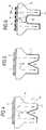
- FIG. 12illustrates schematically a first example of embodiment of a manufacturing method with reference to five intermediate steps 12 a to 12 c [sic].
- a window layer 20 from which the window 1 will later be madeis first made ready, FIG. 12 a.
- the window layer 20can be in the form of a silicon carbide substrate, for example.
- a semiconductor layer sequence 21is applied to the window layer 20 ; in particular it contains an active semiconductor layer that generates radiation in operation.
- the semiconductor layer sequence 21corresponds to the multilayered structure 4 of a semiconductor component pursuant to the invention.
- the sequence of layersis preferably grown epitaxially or applied by a wafer-bonding method.
- An epitaxy processadvantageously reduces the number of manufacturing steps, since attachment to the window layer 20 already occurs with the epitaxial production of the semiconductor layer sequence 21 .
- a wafer-bonding processhas the advantage that materials unsuitable for epitaxy but otherwise beneficial can also be used for the window layer.
- the epitaxy substrate used in the manufacture of the semiconductor layer sequencecan be reused, and the manufacturing costs can thus be reduced.
- the window layer 20is structured, FIG. 12 b .
- the window layer 12 for this purposeis sawed at the parting planes 24 intended for later singling.
- the saw bladehas a shaped edge that is complementary in cross section in the sawing region to the recess 23 to be formed.
- the sawingwould have to occur only between the parting planes 24 .
- the composite of semiconductor layer sequences 21 and window layer 20is then divided into individual semiconductor components by breaking it at the parting planes 24 , with the parts of the window layer 20 constituting the window 1 and the parts of the semiconductor layer sequence 21 applied thereto constituting the multilayered structure 4 .
- FIG. 13shows a second example of embodiment of a manufacturing method pursuant to the invention. Again, the process begins with preparation of a window layer 20 , FIG. 13 a.
- the window layer 20has a first principal face 26 that is intended for the attachment of a semiconductor layer sequence. Structuring is carried out on the second principal face 27 of the window layer.
- the window layer 20is then prestructured before attaching the semiconductor layer sequence 21 , FIG. 13 b .
- the window layer 20is sawed into on the second principal face 27 at the intended parting planes 24 , so that a plurality of recesses 23 is produced, for example with rectangular cross sections.
- the depth of sawing and the depth of the recesses 23are chosen so that the lateral faces to be provided with a contact surface are just exposed. A more extensive, deeper structuring takes place only in a later step of the manufacturing process, so that the mechanical stability of the window layer is largely retained initially.
- the contact metallization 25can preferably be developed at substantially higher temperatures than in the previous example of embodiment. This simplifies or permits sintering of the contact metallization, for example, which likewise advantageously lowers the series resistance of the component.
- a semiconductor layer sequence 21 that contains an active layer 24is applied to the first principal face 26 of the window layer 20 . Since the contact metallization 25 has already been formed, sensitive semiconductor structures in particular can also be formed, for example multiple quantum well structures with low structural thicknesses, which degrade easily at higher temperatures.
- the structuring of the window layer 20 already begunis completed.
- the recesses 23 already formedare deepened and further shaped by sawing again, for example by forming inclined flanks in the window layer to increase radiation output.
- the semiconductor layer sequence 21is also divided into individual multilayered structures 4 .
- An etching method using a known masking technique, for example,is suitable for the structuring of the semiconductor layer sequence 21 .
- FIG. 13 fthe composite of window layers and multilayered structure is singled, as in the preceding example of embodiment.
- FIG. 14A suitable device for applying contact metallization is shown in FIG. 14.
- the devicecontains a source of metal vapor 30 from which the metal vapor 32 escapes in a preferential direction.
- An electron beam vaporizer with a target and an electron beam aimed at this targetcan be used as the source of metal vapor 30 , for example.
- the surface of a window layer 20 to be vapor-metallizedis turned toward the vapor source 30 , with the surface to be metallized being arranged at an angle to the preferential direction of the source of metal vapor 32 .
- the metal vapor 32therefore is deposited on both the principal face 27 and the insides of the recesses 23 .
- the metallized region within the recessesis determined essentially by shadows of projecting edges.
- the depth to which the metal layer is developed inside the recesses 23varies with the slope of the surface to be metallized relative to the preferential direction of the metallization source.
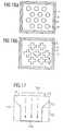
- FIG. 15shows in perspective another example of embodiment of the invention, with the window having flanks with an inclined region 10 a to increase radiation output.
- the multilayered structure 4is also provided with a perforated contact surface 6 that has a plurality of circular openings 14 .
- the contact surfaceitself can be a thick, reflective platinum or palladium contact layer, for example, with the preferred thickness being between 10 nm and 30 nm.
- the contact layer 6can also be of thin form, so that the contact layer 6 is transparent to radiation. The radiation generated is then beneficially output through the openings 14 as well as through the contact layer also.
- FIG. 16shows two plan views of an example of embodiment of the invention with perforated contact surface.
- the openings in the contact layer 6are circular in shape.
- the openingscan also be formed of crossed slits, for example, as shown in FIG. 16 b . It is preferred for the openings to be tightly packed. So that the intermediate regions of the contact surface do not become too narrow and thus impair conduction of current into the component, the crossed-slit openings in FIG. 16 b are arranged so that their mutual separation is no smaller than the arm width a.
- the diameter or arm width a of the openings 14is advantageously of such a dimension that current propagation produces a largely homogeneous current density in the active layer.
Landscapes
- Engineering & Computer Science (AREA)
- Physics & Mathematics (AREA)
- Condensed Matter Physics & Semiconductors (AREA)
- General Physics & Mathematics (AREA)
- Manufacturing & Machinery (AREA)
- Computer Hardware Design (AREA)
- Microelectronics & Electronic Packaging (AREA)
- Power Engineering (AREA)
- Led Devices (AREA)
- Led Device Packages (AREA)
Abstract
Description
- This invention relates to a radiation-emitting semiconductor component pursuant to the preamble of Patent claims 1, 5, 8, and 42, and a method for manufacturing it pursuant to the preamble of[0001]
Patent claim 34. - The invention relates in particular to a radiation-emitting semiconductor component with a nitride-based active multilayered structure applied to a silicon carbide-based epitaxial substrate.[0002]
- Radiation-emitting semiconductor components of the kind mentioned usually have a semiconductor multilayered structure with an active radiation-generating layer that is applied to a carrier transparent to radiation. The radiation is output through the carrier. In this arrangement, however, the radiation yield is sharply reduced by total reflection of the produced radiation at the carrier surface.[0003]
- With block-shaped or cuboid carriers the fraction of totally reflected radiation that cannot be output is especially high because of the orthogonal arrangement of lateral faces and principal faces of the carrier. The radiation yield can be increased by forming recesses in the carrier whose lateral faces are preferably inclined relative to the principal faces of the carrier.[0004]
- A form such as that specified in the priority-determining Patent Application DE 100 067 38.7 is especially beneficial. The contents of this Patent Application are explicitly incorporated in the contents of the present Patent Application.[0005]
- A corresponding component is shown schematically in FIG. 17. The semiconductor component shown has a[0006]
window 151 transparent to radiation, to which is applied a radiation-producingmultilayered structure 152. At least one lateral face of thewindow 151 is configured so that afirst subregion 154 is inclined, concave, or stepped relative to the normal to themultilayered structure 152, which is adjoined by asecond region 155 positioned parallel to the normal to the multilayered structure. There are also twocontact surfaces 153a, b on themultilayered structure 152 on the one hand and on the face of the semiconductor component facing away from themultilayered structure 152 on the other hand. - It is the purpose of this invention to provide a radiation-emitting semiconductor component with improved efficiency. It is also the purpose of the invention to develop a method for manufacturing it. Finally, it is a purpose of the invention to develop a corresponding optical component.[0007]
- This task is achieved by a radiation-emitting semiconductor component pursuant to[0008]
Patent claim Patent claim 34. Beneficial refinements of the invention are objects of the dependent claims. - The invention proceeds from the assumption that the ratio of output radiation power to the electrical power to be supplied for it is critical for the degree of efficiency. The optical output power depends on the degree of output, along with the current flowing through the component. The degree of output indicates how large is the fraction of output radiation relative to the total radiation produced. The electrical power is determined by the current flowing and the series resistance of the component. The degree of efficiency can therefore be increased in particular by lowering the series resistance and by increasing the degree of output.[0009]
- According to the invention, a first form of embodiment provides for forming a radiation-emitting semiconductor component with a multilayered structure, an active layer that generates radiation within the multilayered structure, and a window transparent to radiation with a first principal face and a second principal face opposite the first principal face, with at least one recess being formed in the window to constitute inclined radiation output faces, and at least one lateral surface of the window and/or of the recess being provided with a contact surface. The contact surface preferably also extends over the second principal face of the window or subregions thereof.[0010]
- The current path from the contact surface to the active layer is shortened on the average by this arrangement of the contact surface, and thus beneficially reduces the series resistance of the component.[0011]
- The recess in the invention serves to increase the radiation yield. Either direct output or reflection in a direction favoring output is produced in particular by lateral faces that are inclined relative to the principal faces of the window. A recess in the window means both an indentation in the second principal face of the window or removal of material from an edge of the window, as shown for example in FIG. 15. When material is removed from the edge, the lateral surfaces of the window and of the recess partially coincide.[0012]
- A second contact surface on the multilayered structure is preferably provided for in the invention. This provides for current being fed in close to the active layer within the multilayered structure. It is especially advantageous for this contact surface to be largely transparent to radiation, so that radiation output is also possible through the second contact surface. This can be achieved, for example, by appropriately thin metallization or suitable transparent, electrically conductive films.[0013]
- In a preferred refinement of the invention, the first contact surface is a reflector. Because of this, the portions of the radiation that strike the contact surface from inside the window are not absorbed, but are reflected back, so that subsequent output is possible. Thus a contact surface that is transparent to radiation and one that is reflective contribute to increasing the radiation yield, since they assist the output of radiation either directly or indirectly.[0014]
- A second embodiment of the invention provides forming a radiation-emitting semiconductor component with a multilayered structure, an active layer within the multilayered structure serving to generate radiation, and a window transparent to radiation, with a first principal face and a second principal face opposite the first principal face, with at least one recess being formed in the window to form an inclined radiation output surface. The component here has at least one contact surface with a plurality of openings.[0015]
- It is preferred for at least one of the window surfaces to be provided, at least in part, with a first contact surface and for the multilayered structure to be provided, at least in part, with a second contact surface, with at least one of the contact surfaces having a plurality of openings.[0016]
- It is advantageous also for a plurality of openings to be formed in each of the two contact surfaces.[0017]
- These contact surfaces transparent to radiation, called perforated contact surfaces below, have the advantage over thin contact surfaces transparent to radiation, of higher long-term stability, particularly in a casting composition, for example such as epoxy resin. These perforated contact surfaces can also be made so that they have high transmission in the area of the openings and high reflection in the areas coated with contact material, so that absorption and therefore radiation loss is slight on these contact surfaces.[0018]
- Perforated contact surfaces on the multilayered structure also have the advantage that they do not seal off the multilayered structure, so that for example gases such as hydrogen that reach the multilayered structure during manufacture can diffuse out of it. This also reduces the risk of such gases aggregating at the interface between the multilayered structure and the contact surface, passivating the contact surface, and thus increasing contact resistance and series resistance.[0019]
- The openings in the contact surface(s) are preferably circular, square, rectangular, hexagonal, or in the shape of crossed slits. These forms are especially suitable for a regular arrangement and are comparatively easy to make technically. The openings are preferably packed tightly provided that the intermediate areas of the contact surfaces form a continuous network and the width of the areas meet the requirements for current input into the component. Of course the shapes mentioned do not constitute a limitation of the invention thereto.[0020]
- In an advantageous configuration of the invention in both forms of embodiment, the recess is made in the form of an indentation in the second principal face of the window. It is beneficial that no change of the basic window enveloping shape is necessary, so that in particular production systems, which are often designed for a given basic window shape, can continue to be used without change. A plurality of indentations can also be made in the second principal face, whereby the radiation yield is further increased. This configuration is advantageous especially for large-area semiconductor components, since the ratio of area to circumference rises with increasing chip area, and thus more indentations can be placed in the surface than circumferentially. In a preferred refinement of the invention, the indentation in the second principal face is designed with a triangular, trapezoidal, or semicircular cross section (section perpendicular to the second principal face). The cross section can also have the shape of a rectangle with added triangle, trapezoid, or semicircle. In general the formation of recesses with at least one lateral face not in an orthogonal position to the principal faces is advantageous. Depending on the specific form of embodiment, the angle of incidence of the radiation produced relative to the normal to the lateral faces, and thus the fraction of totally reflected radiation, is thereby lowered, or reflection toward the flanks of the window is brought about, so that direct output or at least output after further reflections can take place. The latter applies in particular to the lateral faces of the indentation that are provided with a reflective contact surface.[0021]
- The indentation in the second principal face of the window is preferably in the form of a trough with one of the aforementioned cross-sectional shapes. Such an indentation can be made, for example, by sawing into the window from the second principal face and using a saw blade with shaped rim. If this sawing is performed in the wafer composite, then a plurality of windows can advantageously be structured in one production step.[0022]
- Alternatively, the indentations can also be etched in place. In this form of embodiment in particular, spatially isolated indentation shapes bordered all around can be formed. The structuring of a plurality of windows in the wafer composite in one production step is also advantageously possible here.[0023]
- In an especially preferred refinement of the invention, the recess that increases radiation yield is formed at the edge of the second principal face and is so shaped that the window is tapered down toward the second principal face. It is preferred for the recess to be made so that the lateral faces of the recess have a first subregion inclined relative to the normal to the multilayered structure in the vicinity of the multilayered structure, that changes at greater distance from the multilayered structure to a second subregion running parallel to the normal to the multilayered structure.[0024]
- The window is preferably formed as a parallelepiped in the section corresponding to the second region. It is advantageous that the radiation yield is increased by the inclined subregion, while the remaining area of the window has a square basic shape and thus can easily be mounted. In this case in particular, the lateral faces [of] the second subregion are provided with a contact surface. The contact surface can also extend over the first subregion of the lateral faces, and can then preferably be made reflective, so that the radiation yield toward the multilayered structure is increased by reflection of the radiation produced.[0025]
- The described structure can be formed advantageously at low production cost, for example by sawing a wafer with a saw blade with shaped edge to isolate the semiconductor bodies, and then singling the semiconductor bodies by breaking the wafer. Prior sawing of the wafer is desirable to facilitate singling by breaking. The described window shape can be excavated at the same time by using a suitable saw blade with shaped edge. Other advantageous configurations in this regard are specified in DE 100 067 38.7, to which this invention refers in particular.[0026]
- A manufacturing method pursuant to the invention begins with preparation of a window layer, from which the actual window will later be produced.[0027]
- A semiconductor layer sequence corresponding to the multilayered structure is applied to the window layer. It is preferably applied epitaxially or in the context of a wafer-bonding procedure. In epitaxy, the window layer at the same time advantageously represents the epitaxy substrate. In a wafer-bonding procedure, the semiconductor layer sequence is produced first on a suitable substrate, and is then bonded to the window layer. Materials that are unsuitable for an epitaxial process can also advantageously be used here as window material.[0028]
- In another step the window layer is structured to develop the recess in a suitable manner. Structuring can be accomplished, for example as described, by sawing or etching the window layer. Structuring can also be performed in multiple steps, not necessarily in succession. Thus, with regard to the mechanical breakage stability of the window layer, it is advantageous to first prestructure the window layer and to perform the final structuring only at a later stage of the production process.[0029]
- In a further step the contact surfaces are applied to the window layer. The contact surfaces are preferably vapor-deposited or sputtered on for contact metallization.[0030]
- Finally, the semiconductor components are completed. This includes in particular the singling of the composite of window layer and semiconductor layer sequence into a plurality of windows with multilayered structure located thereon. The singling is performed preferably by sawing and/or breaking the window layer. Additional contact surfaces, for example contact metallizations, can also be applied to the multilayered structure in the course of completion.[0031]
- To perform the contact metallization, vapor deposition systems are ordinarily used, from which the metal vapor originates with a given preferential direction. It is advantageous in this case to arrange the surface of the window layer to be subjected to vapor deposition at an angle to this preferential direction. In this way, deposition of the metal vapor on the second principal face of the window layer and also on the lateral faces of the recesses formed by the structuring is achieved.[0032]
- With regard to the sequence of the described manufacturing steps, three alternatives described below are distinguished by particular advantages:[0033]
- In the first advantageous alternative, the semiconductor layer sequence is first applied to the window layer, the window layer is then structured, and finally it is subjected to vapor deposition to develop the contact surfaces. Especially in case of epitaxial production of the semiconductor layer sequence, existing production equipment can be used for this without changes, since with epitaxy the window layer does not yet differ from window layers pursuant to the state of the art. Furthermore, the window layer is structured only at the end of the manufacturing process, so that the risk of breakage of the window layer in the preceding steps is comparatively slight.[0034]
- A process in which the window layer is first structured and provided with contact surfaces represents a second advantageous alternative. The semiconductor layer sequence is then applied. In this case, higher temperatures such as those necessary for sintering certain contact metallizations can be used to perform the contact metallization. These temperatures are usually so high that the semiconductor layer sequence would be damaged by them. Therefore, such damage is avoided by performing the contact metallization at the beginning of the manufacturing process.[0035]
- In a third advantageous alternative manufacturing process, the structuring of the window layer takes place in two steps. To this end, the window layer is first prestructured to the extent necessary for developing the contact surfaces on the lateral faces. The contact surfaces are then developed, for example by vapor deposition. The semiconductor layer sequence is then applied to the window layer prestructured in this way and provided with contact surfaces. The window layer is then subjected to final structuring. This second structuring step is preferably combined with isolation of the components, for example by sawing the window layer with a shaped saw blade, and then breaking it apart. To minimize the risk of breaking the structured window layer, the window layer can also be mounted on a suitable auxiliary support.[0036]
- Other features, benefits, and suitabilities of the invention will be explained below with reference to examples of embodiment in combination with FIGS.[0037]1 to16.
- The figures show:[0038]
- FIG. 1 a schematic cross sectional illustration of a first example of embodiment of a semiconductor component pursuant to the invention,[0039]
- FIG. 2 a schematic cross sectional illustration of a second example of embodiment of a semiconductor component pursuant to the invention,[0040]
- FIG. 3 a schematic cross sectional illustration of a third example of embodiment of a semiconductor component pursuant to the invention,[0041]
- FIG. 4 a schematic cross sectional illustration of a fourth example of embodiment of a semiconductor component pursuant to the invention,[0042]
- FIG. 5 a schematic cross sectional illustration of a fifth example of embodiment of a semiconductor component pursuant to the invention,[0043]
- FIG. 6 a schematic cross sectional illustration of a sixth example of embodiment of a semiconductor component pursuant to the invention,[0044]
- FIG. 7 a schematic cross sectional illustration of a seventh example of embodiment of a semiconductor component pursuant to the invention,[0045]
- FIG. 8 a schematic cross sectional illustration of an eighth example of embodiment of a semiconductor component pursuant to the invention,[0046]
- FIG. 9 a schematic cross sectional illustration of a ninth example of embodiment of a semiconductor component pursuant to the invention,[0047]
- FIG. 10 a schematic cross sectional illustration of a tenth example of embodiment of a semiconductor component pursuant to the invention,[0048]
- FIG. 11 a schematic cross sectional illustration of an eleventh example of embodiment of a semiconductor component pursuant to the invention,[0049]
- FIG. 12 a schematic perspective illustration of a twelfth example of embodiment of a semiconductor component pursuant to the invention,[0050]
- FIG. 13 a schematic illustration of a thirteenth example of embodiment of a semiconductor component pursuant to the invention,[0051]
- FIG. 14 a schematic illustration of a first example of embodiment of a manufacturing process pursuant to the invention in five intermediate steps,[0052]
- FIG. 15 a schematic illustration of a second example of embodiment of a manufacturing process pursuant to the invention in six intermediate steps,[0053]
- FIG. 16 a device for implementing an intermediate step in the examples of embodiment of a manufacturing process pursuant to the invention, and[0054]
- FIG. 17 a schematic illustration of a radiation-emitting semiconductor component pursuant to the priority-determining Patent Application DE 100 067 38.7.[0055]
- The example of embodiment shown in FIG. 1 has a[0056]
window 1 with a firstprincipal face 2 and a secondprincipal face 3. Amultilayered structure 4 with anactive layer 5 that emits radiation during operation is applied to the firstprincipal face 2 and is coated with acontact metallization 6. - The[0057]
window 1 itself is formed from a cuboid base form7 rectangular in cross section that hasrecesses 8 on its circumference. The window flanks10 thus produced also correspond to the lateral faces of the recess and have afirst subregion 10athat is arranged at an angle to the principal faces2,3 of the window and that changes into asecond subregion 10borthogonal to the principal faces at a greater distance from themultilayered structure 4. - In this[0058]
second subregion 10b,the window flanks are provided withcontact metallization 11 that also covers the secondprincipal face 3 of thewindow 1. Thecurrent paths 12 from the active layer to thecontact surface 11 are shortened on the average by thecontact surface 11 raised on thewindow flank 10b,and thus the series resistance of the component is advantageously lowered. The radiation is preferably output in theinclined region 10aof the window flanks. - In the example of embodiment shown in FIG. 2 the[0059]
contact metallization 11 extends over theinclined subregions 10aof the window flanks. This achieves a further shortening of thecurrent paths 12 and thus a reduction of series resistance. Of course thesubregions 10aare then no longer available for direct radiation output. In this example of embodiment, therefore, thecontact metallization 11 is made reflective so that the fractions of radiation emitted into the window for the most part are again reflected toward themultilayered structure 4 and are subsequently output. This is made clear by way of example by thebeams - In the third example of embodiment shown in FIG. 3, in contrast to the examples of embodiment described above, the[0060]
recess 8 runs through the center of the secondprincipal face 3 as a central indentation. Thecontact metallization 11 is developed over the entire area over the secondprincipal face 3 and the lateral faces of theindentation 8. Thecurrent path 12 to the active layer is shortened in this way within theindentation 8, and the series resistance of the component is reduced. The contact metallization can again be made reflective to increase the radiation yield. - FIG. 4 shows a fourth example of embodiment, in which the envelope of the first example of embodiment is advantageously combined with the central indentation of the third example of embodiment. In this way the series resistance is advantageously lowered by the shortening of the[0061]
current path 12 as in the third example of embodiment, with the window flank being available at the same time for output of radiation. In addition, because of thecentral indentation 8 withreflective contact metallization 11, the radiation yield is increased by theradiation fractions 13 reflected out laterally. - In the firth example of embodiment shown in FIG. 5, the[0062]
contact metallization 11 extends both across thecentral indentation 8 in the second principal face of thewindow 1 and across subregions of the window flanks10. Compared to the fourth example of embodiment, the series resistance is lowered further in this way, with this entailing a reduced radiation yield in the area of the contact metallization. Depending on how the parameters of series resistance and radiation yield are weighted, the fourth or the fifth example of embodiment may be more advantageous, with the transition between these two examples of embodiment being continuous depending on the extent of the contact metallization on the window flanks. - The radiation yield can be increased by reflection at the[0063]
central indentation 8 in the secondprincipal face 3 in various ways. One possibility has already been shown in the context of the fourth example of embodiment in FIG. 4,beam 13c.If the angle of opening of thecentral indentation 8 is enlarged, the result is to increase reflection toward themultilayered structure 4 and thus output through themultilayered structure 4. - This is illustrated in the sixth example of embodiment in FIG. 6 with reference to the[0064]
beam 13d.Aside from thecentral indentation 8, this example of embodiment corresponds to the fourth example of embodiment, FIG. 4. Thecentral indentation 8, on the other hand, is cut distinctly deeper than in FIG. 4 and has a five-cornered cross section, which is composed of a rectangle with added triangle. The angle of opening of the triangle is greater than shown in the example of embodiment illustrated in FIG. 4 and causes increased reflection toward themultilayered structure 4. It is advantageous in this case to perforate thecontact surface 6 on the multilayered structure and thus enlarge the output through this contact surface. - The deeply cut and completely metallized[0065]
recess 8 also leads to an especially great shortening of thecurrent path 12 because of the closeness of the bottom face of the recess to themultilayered structure 4. - In the seventh example of embodiment illustrated in FIG. 7, in contrast to the sixth example of embodiment, the angle of opening of the central recess is chosen to be smaller. This leads to increased reflection toward the inclined lateral[0066]
window face sections 10a, and in connection with this to increased output on the part of themultilayered structure 4. It is also advantageous here to perforate thecontact surface 6 on themultilayered structure 4. Various beam paths are shown schematically by thebeams 13. - In the eighth example of embodiment shown in FIG. 8, in contrast to the prior examples of embodiment, only the second[0067]
principal face 3 and themultilayered structure 4 are provided with contact surfaces, with thecontact surface 6 on the multilayered structure being perforated. This achieves particularly high radiation output through the lateral faces10. Thecentral indentation 8 is designed so that total reflection occurs on a portion of its lateral faces. - In the examples of embodiment shown in FIGS. 9 and 10, the lateral faces of the window are partially provided with perforated contact surfaces. With these, radiation output is also advantageously possible in the area of these contact surfaces, with series resistance being beneficially reduced by the reduction of the distance between the contact surfaces[0068]6 and11. In the example of embodiment shown in FIG. 9, the contact surface also extends over the
central recess 8. In the example of embodiment according to FIG. 10, on the other hand, the central recess is uncoated, to reduce manufacturing costs, and theradiation 13 is totally reflected on the inside of thecentral recess 8. - FIG. 11 illustrates another example of embodiment, which in contrast to the previously described examples of embodiment has two[0069]
central recesses 8a, b.Therecesses 8a, band thecontact metallization 11 on them correspond in shape to the sixth example of embodiment; naturally combination with the other shown examples of embodiment is likewise possible. The multiple arrangement of recesses in the secondprincipal face 3 is advantageous especially for large-area semiconductor components, since both the series resistance of the component can be lowered and the radiation yield over the entire component can be increased with a plurality of recesses. Of course more than the tworecesses 8a, b can also be made if the stability of the component permits. - In the examples of embodiment, the[0070]
window 1 preferably consists of silicon carbide onto which a gallium nitride-based multilayered structure is applied. Silicon carbide is preferably used as the epitaxy substrate for gallium nitrite-based [sic] semiconductor elements. Gallium nitride-based materials here, besides GaN itself, means materials derived from or related to GaN, in particular ternary or quaternary mixed crystal systems such as AlGaN (Al1-xGaxN, 0≦x≦1), InGaN (In1-xGaxN, 0≦x≦1), InAlN (In1-xAlxN, 0≦x≦1), and AlInGaN (Al1-x-yInxGayN, 0≦x≦1, 0≦y≦1). - The epitaxial production of such gallium nitride-based components requires a substrate largely matching the gallium nitride lattice, for which silicon carbide is especially suitable.[0071]
- Of course silicon carbide has a very high index of refraction of about 2.7, so that the total reflection losses are correspondingly high and the degree of output is correspondingly low. The shown examples of embodiment advantageously increase the radiation yield, especially because of the inclined lateral faces. The series resistance of the component, increased in principle by the reduced cross section of the window, is compensated for, or furthermore even lowered, by the laterally raised contact surfaces. Providing reflective, semi-transparent or perforated contact metallizations contributes to further increasing the radiation yield.[0072]
- However, the invention is not limited to gallium nitride-based systems, but can also be used with other semiconductor systems, for example such as materials based on gallium arsenide, gallium phosphide, or zinc selenide. Here also, a substantial fraction of the radiation generated remains in the multilayered structure-window arrangement because of total reflection and is ultimately absorbed.[0073]
- The invention is also beneficial for window materials other than those mentioned so far, for example materials based on quartz glass, diamond, ITO (indium tin oxide), or on zinc oxide, tin oxide, indium oxide, or gallium phosphide, since as a rule with all of these windows there is a transition to an optically thinner medium by which total reflection can occur and the degree of output is accordingly reduced.[0074]
- The invention is also advantageous for potted semiconductor bodies and windows or for those otherwise provided with a covering, since the covering as a rule has a lower index of refraction so that in this case also, the radiation yield is reduced by total reflection.[0075]
- A window made of the materials mentioned can be applied to the multilayered structure after the multilayered structure is produced. In epitaxial production of the multilayered structure, this is possible, for example, by detaching the epitaxy substrate after the epitaxy and bonding the window to the multilayered structure in its place by a wafer-bonding process.[0076]
- Alternatively, the window can also be applied to the epitaxially manufactured semiconductor surface and the epitaxy substrate then detached thereafter. This procedure has the advantage that the epitaxy substrate can be reused, which leads to a clear cost benefit especially in the case of expensive materials, for example silicon carbide substrates in this case.[0077]
- FIG. 12 illustrates schematically a first example of embodiment of a manufacturing method with reference to five intermediate steps[0078]12ato12c[sic].
- A[0079]
window layer 20 from which thewindow 1 will later be made is first made ready, FIG. 12a.Thewindow layer 20 can be in the form of a silicon carbide substrate, for example. - A[0080]
semiconductor layer sequence 21 is applied to thewindow layer 20; in particular it contains an active semiconductor layer that generates radiation in operation. Thesemiconductor layer sequence 21 corresponds to themultilayered structure 4 of a semiconductor component pursuant to the invention. The sequence of layers is preferably grown epitaxially or applied by a wafer-bonding method. An epitaxy process advantageously reduces the number of manufacturing steps, since attachment to thewindow layer 20 already occurs with the epitaxial production of thesemiconductor layer sequence 21. On the other hand, a wafer-bonding process has the advantage that materials unsuitable for epitaxy but otherwise beneficial can also be used for the window layer. In addition, the epitaxy substrate used in the manufacture of the semiconductor layer sequence can be reused, and the manufacturing costs can thus be reduced. - After attaching the[0081]
semiconductor layer sequence 21, thewindow layer 20 is structured, FIG. 12b. In the example of embodiment shown, thewindow layer 12 for this purpose is sawed at the parting planes24 intended for later singling. The saw blade has a shaped edge that is complementary in cross section in the sawing region to therecess 23 to be formed. To make a central indentation, as illustrated by way of example in the third example of embodiment, the sawing would have to occur only between the parting planes24. - [0082]
Overall metallization 25 is then performed on the structuredwindow layer 20. This step will be explained in greater detail below. - The composite of[0083]
semiconductor layer sequences 21 andwindow layer 20 is then divided into individual semiconductor components by breaking it at the parting planes24, with the parts of thewindow layer 20 constituting thewindow 1 and the parts of thesemiconductor layer sequence 21 applied thereto constituting themultilayered structure 4. - FIG. 13 shows a second example of embodiment of a manufacturing method pursuant to the invention. Again, the process begins with preparation of a[0084]
window layer 20, FIG. 13a.Thewindow layer 20 has a firstprincipal face 26 that is intended for the attachment of a semiconductor layer sequence. Structuring is carried out on the secondprincipal face 27 of the window layer. - The[0085]
window layer 20 is then prestructured before attaching thesemiconductor layer sequence 21, FIG. 13b. For this purpose thewindow layer 20 is sawed into on the secondprincipal face 27 at the intended parting planes24, so that a plurality ofrecesses 23 is produced, for example with rectangular cross sections. The depth of sawing and the depth of therecesses 23 are chosen so that the lateral faces to be provided with a contact surface are just exposed. A more extensive, deeper structuring takes place only in a later step of the manufacturing process, so that the mechanical stability of the window layer is largely retained initially. - The[0086]
recesses 23 formed in this way and the remaining areas of the secondprincipal face 27 are then provided withcontinuous contact metallization 25. Since there are still no semiconductor layers on thewindow layer 20, thecontact metallization 25 can preferably be developed at substantially higher temperatures than in the previous example of embodiment. This simplifies or permits sintering of the contact metallization, for example, which likewise advantageously lowers the series resistance of the component. - In the next step, as in the example of embodiment described previously, a[0087]
semiconductor layer sequence 21 that contains anactive layer 24 is applied to the firstprincipal face 26 of thewindow layer 20. Since thecontact metallization 25 has already been formed, sensitive semiconductor structures in particular can also be formed, for example multiple quantum well structures with low structural thicknesses, which degrade easily at higher temperatures. - This is followed by another structuring step in which the structuring of the[0088]
window layer 20 already begun is completed. Therecesses 23 already formed are deepened and further shaped by sawing again, for example by forming inclined flanks in the window layer to increase radiation output. In addition, thesemiconductor layer sequence 21 is also divided into individualmultilayered structures 4. An etching method using a known masking technique, for example, is suitable for the structuring of thesemiconductor layer sequence 21. - In the last step, FIG. 13[0089]f, the composite of window layers and multilayered structure is singled, as in the preceding example of embodiment.
- In the described manufacturing method it is necessary to provide structured surfaces, for example the[0090]
surface 27 and therecesses 23 formed in it in FIG. 12, with a uniform contact surface. These structured surfaces are composed of a plurality of individual surfaces joined at an angle, which makes it difficult to develop a contact surface. A suitable device for applying contact metallization is shown in FIG. 14. The device contains a source ofmetal vapor 30 from which themetal vapor 32 escapes in a preferential direction. An electron beam vaporizer with a target and an electron beam aimed at this target can be used as the source ofmetal vapor 30, for example. - The surface of a[0091]
window layer 20 to be vapor-metallized is turned toward thevapor source 30, with the surface to be metallized being arranged at an angle to the preferential direction of the source ofmetal vapor 32. Themetal vapor 32 therefore is deposited on both theprincipal face 27 and the insides of therecesses 23. The metallized region within the recesses is determined essentially by shadows of projecting edges. The depth to which the metal layer is developed inside therecesses 23 varies with the slope of the surface to be metallized relative to the preferential direction of the metallization source. - FIG. 15 shows in perspective another example of embodiment of the invention, with the window having flanks with an[0092]
inclined region 10ato increase radiation output. Themultilayered structure 4 is also provided with aperforated contact surface 6 that has a plurality ofcircular openings 14. The contact surface itself can be a thick, reflective platinum or palladium contact layer, for example, with the preferred thickness being between 10 nm and 30 nm. - Alternatively, the[0093]
contact layer 6 can also be of thin form, so that thecontact layer 6 is transparent to radiation. The radiation generated is then beneficially output through theopenings 14 as well as through the contact layer also. - FIG. 16 shows two plan views of an example of embodiment of the invention with perforated contact surface. In the example of embodiment illustrated in FIG. 16[0094]a, the openings in the
contact layer 6 are circular in shape. Alternatively, the openings can also be formed of crossed slits, for example, as shown in FIG. 16b. It is preferred for the openings to be tightly packed. So that the intermediate regions of the contact surface do not become too narrow and thus impair conduction of current into the component, the crossed-slit openings in FIG. 16bare arranged so that their mutual separation is no smaller than the arm width a. - The diameter or arm width a of the[0095]
openings 14 is advantageously of such a dimension that current propagation produces a largely homogeneous current density in the active layer. - The explanation of the invention with reference to the shown examples of embodiment naturally does not represent any limitation of the invention to these examples of embodiment.[0096]
Claims (61)
Priority Applications (1)
| Application Number | Priority Date | Filing Date | Title |
|---|---|---|---|
| US11/684,347US20070145402A1 (en) | 2000-02-15 | 2007-03-09 | Semiconductor component which emits radiation, and method for producing the same |
Applications Claiming Priority (7)
| Application Number | Priority Date | Filing Date | Title |
|---|---|---|---|
| DE10006738 | 2000-02-15 | ||
| DE10006738ADE10006738C2 (en) | 2000-02-15 | 2000-02-15 | Light-emitting component with improved light decoupling and method for its production |
| DE10006738.7 | 2000-02-15 | ||
| DE10025448.9 | 2000-05-23 | ||
| DE10025448 | 2000-05-23 | ||
| DE10025448 | 2000-05-23 | ||
| PCT/DE2001/000600WO2001061765A1 (en) | 2000-02-15 | 2001-02-15 | Semiconductor component which emits radiation, and method for producing the same |
Related Child Applications (1)
| Application Number | Title | Priority Date | Filing Date |
|---|---|---|---|
| US11/684,347DivisionUS20070145402A1 (en) | 2000-02-15 | 2007-03-09 | Semiconductor component which emits radiation, and method for producing the same |
Publications (2)
| Publication Number | Publication Date |
|---|---|
| US20030127654A1true US20030127654A1 (en) | 2003-07-10 |
| US7205578B2 US7205578B2 (en) | 2007-04-17 |
Family
ID=26004340
Family Applications (2)
| Application Number | Title | Priority Date | Filing Date |
|---|---|---|---|
| US10/203,728Expired - LifetimeUS7205578B2 (en) | 2000-02-15 | 2001-02-15 | Semiconductor component which emits radiation, and method for producing the same |
| US11/684,347AbandonedUS20070145402A1 (en) | 2000-02-15 | 2007-03-09 | Semiconductor component which emits radiation, and method for producing the same |
Family Applications After (1)
| Application Number | Title | Priority Date | Filing Date |
|---|---|---|---|
| US11/684,347AbandonedUS20070145402A1 (en) | 2000-02-15 | 2007-03-09 | Semiconductor component which emits radiation, and method for producing the same |
Country Status (6)
| Country | Link |
|---|---|
| US (2) | US7205578B2 (en) |
| EP (2) | EP1256135A1 (en) |
| JP (1) | JP5231701B2 (en) |
| CN (1) | CN100521257C (en) |
| AU (1) | AU2001239182A1 (en) |
| WO (1) | WO2001061765A1 (en) |
Cited By (17)
| Publication number | Priority date | Publication date | Assignee | Title |
|---|---|---|---|---|
| US20040046179A1 (en)* | 2001-03-09 | 2004-03-11 | Johannes Baur | Radiation-emitting semiconductor component and method for producing the semiconductor component |
| US20050164482A1 (en)* | 2004-01-22 | 2005-07-28 | Cree, Inc. | Silicon Carbide on Diamond Substrates and Related Devices and Methods |
| US20060075958A1 (en)* | 2004-09-21 | 2006-04-13 | Adrian Powell | Low basal plane dislocation bulk grown SiC wafers |
| US20060097271A1 (en)* | 2002-07-31 | 2006-05-11 | Osram Opto Semiconductors Gmbh | Gan-based radiation-emitting thin-layered semiconductor component |
| US20060225645A1 (en)* | 2005-04-07 | 2006-10-12 | Adrian Powell | Three inch silicon carbide wafer with low warp, bow, and TTV |
| WO2006109222A1 (en)* | 2005-04-13 | 2006-10-19 | Philips Intellectual Property & Standards Gmbh | Structured substrate for a led |
| US20060255364A1 (en)* | 2004-02-05 | 2006-11-16 | Saxler Adam W | Heterojunction transistors including energy barriers and related methods |
| US20070145402A1 (en)* | 2000-02-15 | 2007-06-28 | Dominik Eisert | Semiconductor component which emits radiation, and method for producing the same |
| US20080035941A1 (en)* | 2003-09-26 | 2008-02-14 | Volker Harle | Radiation-Emitting Thin-Film Semiconductor Chip |
| EP2085675A1 (en) | 2008-01-31 | 2009-08-05 | MAT Mischanlagentechnik GmbH | Connecting device |
| US7592211B2 (en) | 2006-01-17 | 2009-09-22 | Cree, Inc. | Methods of fabricating transistors including supported gate electrodes |
| US7709269B2 (en) | 2006-01-17 | 2010-05-04 | Cree, Inc. | Methods of fabricating transistors including dielectrically-supported gate electrodes |
| US20100264434A1 (en)* | 2005-09-29 | 2010-10-21 | Andreas Ploessl | Optoelectronic Semiconductor Chip |
| US20100308365A1 (en)* | 2008-02-07 | 2010-12-09 | Showa Denko K.K. | Compound semiconductor light emitting diode |
| WO2014108821A1 (en)* | 2013-01-10 | 2014-07-17 | Koninklijke Philips N.V. | Led with shaped growth substrate for side emission |
| WO2015118419A1 (en)* | 2014-02-06 | 2015-08-13 | Koninklijke Philips N.V. | Light emitting diode with structured substrate |
| US9887319B2 (en)* | 2012-02-09 | 2018-02-06 | Oculus Vr, Llc | Enhanced light extraction |
Families Citing this family (30)
| Publication number | Priority date | Publication date | Assignee | Title |
|---|---|---|---|---|
| JP3864670B2 (en)* | 2000-05-23 | 2007-01-10 | 豊田合成株式会社 | Method for manufacturing group III nitride compound semiconductor light emitting device |
| DE10056292A1 (en) | 2000-11-14 | 2002-09-19 | Osram Opto Semiconductors Gmbh | emitting diode |
| DE10139798B9 (en)* | 2001-08-14 | 2006-12-28 | Osram Opto Semiconductors Gmbh | Radiation-emitting component with geometrically optimized coupling-out structure |
| US6635503B2 (en)* | 2002-01-28 | 2003-10-21 | Cree, Inc. | Cluster packaging of light emitting diodes |
| TWI236772B (en)* | 2002-03-14 | 2005-07-21 | Toshiba Corp | Semiconductor light emitting element and semiconductor light emitting device |
| CN100552987C (en)* | 2002-05-28 | 2009-10-21 | 松下电工株式会社 | Light emitting device, lighting apparatus using the same, and surface light emitting lighting apparatus |
| JP2004056088A (en)* | 2002-05-31 | 2004-02-19 | Toyoda Gosei Co Ltd | Group III nitride compound semiconductor light emitting device |
| JP4116387B2 (en)* | 2002-09-30 | 2008-07-09 | 株式会社東芝 | Semiconductor light emitting device |
| DE10253911A1 (en)* | 2002-09-30 | 2004-04-08 | Osram Opto Semiconductors Gmbh | Radiation-emitting semiconductor component and method for its production |
| US7592636B2 (en) | 2002-09-30 | 2009-09-22 | Osram Opto Semiconductors Gmbh | Radiation-emitting semiconductor component and method for the production thereof |
| DE102004036295A1 (en) | 2003-07-29 | 2005-03-03 | GELcore, LLC (n.d.Ges.d. Staates Delaware), Valley View | Fabrication of flip-chip light emitting diode device by fabricating light emitting diode devices on epitaxial wafer, dicing the epitaxial wafer, flip chip bonding the device die to mount, and reducing thickness of growth substrate |
| DE10339982B4 (en)* | 2003-08-29 | 2009-10-08 | Osram Opto Semiconductors Gmbh | Method for applying an antireflection layer to a plurality of radiation-emitting semiconductor chips |
| JP4259268B2 (en)* | 2003-10-20 | 2009-04-30 | 豊田合成株式会社 | Semiconductor light emitting device |
| WO2005062905A2 (en) | 2003-12-24 | 2005-07-14 | Gelcore Llc | Laser lift-off of sapphire from a nitride flip-chip |
| US7125734B2 (en) | 2005-03-09 | 2006-10-24 | Gelcore, Llc | Increased light extraction from a nitride LED |
| JP2007042857A (en)* | 2005-08-03 | 2007-02-15 | Nichia Chem Ind Ltd | Semiconductor light emitting device, method for manufacturing semiconductor device, and semiconductor light emitting device |
| DE102006015788A1 (en) | 2006-01-27 | 2007-09-13 | Osram Opto Semiconductors Gmbh | Optoelectronic semiconductor chip |
| JP4948307B2 (en)* | 2006-07-31 | 2012-06-06 | 三洋電機株式会社 | Semiconductor laser device and manufacturing method thereof |
| JP5340583B2 (en)* | 2007-11-26 | 2013-11-13 | スタンレー電気株式会社 | Semiconductor light emitting device |
| TW200945633A (en)* | 2008-02-27 | 2009-11-01 | Alps Electric Co Ltd | Light emitter and semiconductor light-emitting device using same |
| DE102010032041A1 (en) | 2010-07-23 | 2012-01-26 | Osram Opto Semiconductors Gmbh | Radiation-emitting component and method for the production of radiation-emitting Bauelemnenten |
| JP5201229B2 (en)* | 2011-02-21 | 2013-06-05 | 日亜化学工業株式会社 | Manufacturing method of semiconductor device |
| US10096742B2 (en) | 2012-03-28 | 2018-10-09 | Sensor Electronic Technology, Inc. | Light emitting device substrate with inclined sidewalls |
| WO2013148955A1 (en)* | 2012-03-28 | 2013-10-03 | Sensor Electronic Technology, Inc. | Light emitting device substrate with inclined sidewalls |
| CN103107259B (en)* | 2013-02-22 | 2015-10-14 | 厦门市三安光电科技有限公司 | Method for manufacturing light-emitting diode chip |
| JP6255255B2 (en)* | 2014-01-27 | 2017-12-27 | 株式会社ディスコ | Optical device processing method |
| US20160013363A1 (en) | 2014-07-08 | 2016-01-14 | Epistar Corporation | Light-emitting element and the manufacturing method thereof |
| JP6569291B2 (en)* | 2015-05-13 | 2019-09-04 | 日亜化学工業株式会社 | Light emitting element |
| DE102015119553A1 (en) | 2015-11-12 | 2017-05-18 | Osram Opto Semiconductors Gmbh | Radiation-emitting semiconductor chip, optoelectronic component with a radiation-emitting semiconductor chip and method for coating a radiation-emitting semiconductor chip |
| DE102016112584B4 (en) | 2016-07-08 | 2024-10-24 | OSRAM Opto Semiconductors Gesellschaft mit beschränkter Haftung | Semiconductor chip, method for producing a semiconductor chip and device with a plurality of semiconductor chips |
Citations (29)
| Publication number | Priority date | Publication date | Assignee | Title |
|---|---|---|---|---|
| US3202543A (en)* | 1962-06-01 | 1965-08-24 | Ibm | Method of forming a thin film grid |
| US4459100A (en)* | 1980-05-01 | 1984-07-10 | Philip Morris Incorporated | Process for expansion of tobacco |
| US4965223A (en)* | 1987-11-18 | 1990-10-23 | Hewlett-Packard Company | Method of manufacturing a partially opaque substrate red led |
| US5087949A (en)* | 1989-06-27 | 1992-02-11 | Hewlett-Packard Company | Light-emitting diode with diagonal faces |
| US5233204A (en)* | 1992-01-10 | 1993-08-03 | Hewlett-Packard Company | Light-emitting diode with a thick transparent layer |
| US5309001A (en)* | 1991-11-25 | 1994-05-03 | Sharp Kabushiki Kaisha | Light-emitting diode having a surface electrode of a tree-like form |
| US5349211A (en)* | 1992-03-26 | 1994-09-20 | Nec Corporation | Semiconductor infrared emitting device with oblique side surface with respect to the cleavage |
| US5387804A (en)* | 1988-12-28 | 1995-02-07 | Sharp Kabushiki Kaisha | Light emitting diode |
| US5547906A (en)* | 1992-09-14 | 1996-08-20 | Badehi; Pierre | Methods for producing integrated circuit devices |
| US5563422A (en)* | 1993-04-28 | 1996-10-08 | Nichia Chemical Industries, Ltd. | Gallium nitride-based III-V group compound semiconductor device and method of producing the same |
| US5585648A (en)* | 1995-02-03 | 1996-12-17 | Tischler; Michael A. | High brightness electroluminescent device, emitting in the green to ultraviolet spectrum, and method of making the same |
| US5744828A (en)* | 1995-07-13 | 1998-04-28 | Kabushiki Kaisha Toshiba | Semiconductor light emitting device with blocking layer |
| US5753940A (en)* | 1995-10-16 | 1998-05-19 | Kabushiki Kaisha Toshiba | Light-emitting diode having narrow luminescence spectrum |
| US5753966A (en)* | 1995-12-25 | 1998-05-19 | Sony Corporation | Semiconductor device with cleaved surface |
| US5779924A (en)* | 1996-03-22 | 1998-07-14 | Hewlett-Packard Company | Ordered interface texturing for a light emitting device |
| US5821568A (en)* | 1995-12-19 | 1998-10-13 | Sony Corporation | Cleaved semiconductor device with {11-20} plane |
| US5864171A (en)* | 1995-03-30 | 1999-01-26 | Kabushiki Kaisha Toshiba | Semiconductor optoelectric device and method of manufacturing the same |
| US5998232A (en)* | 1998-01-16 | 1999-12-07 | Implant Sciences Corporation | Planar technology for producing light-emitting devices |
| US6040235A (en)* | 1994-01-17 | 2000-03-21 | Shellcase Ltd. | Methods and apparatus for producing integrated circuit devices |
| US6117707A (en)* | 1994-07-13 | 2000-09-12 | Shellcase Ltd. | Methods of producing integrated circuit devices |
| US6143588A (en)* | 1997-09-09 | 2000-11-07 | Amkor Technology, Inc. | Method of making an integrated circuit package employing a transparent encapsulant |
| US6168965B1 (en)* | 1999-08-12 | 2001-01-02 | Tower Semiconductor Ltd. | Method for making backside illuminated image sensor |
| US6194743B1 (en)* | 1997-12-15 | 2001-02-27 | Agilent Technologies, Inc. | Nitride semiconductor light emitting device having a silver p-contact |
| US6229160B1 (en)* | 1997-06-03 | 2001-05-08 | Lumileds Lighting, U.S., Llc | Light extraction from a semiconductor light-emitting device via chip shaping |
| US6291839B1 (en)* | 1998-09-11 | 2001-09-18 | Lulileds Lighting, U.S. Llc | Light emitting device having a finely-patterned reflective contact |
| US6329224B1 (en)* | 1998-04-28 | 2001-12-11 | Tessera, Inc. | Encapsulation of microelectronic assemblies |
| US6429462B1 (en)* | 1998-12-29 | 2002-08-06 | D-Led Corporation | Injection incoherent emitter |
| US6459100B1 (en)* | 1998-09-16 | 2002-10-01 | Cree, Inc. | Vertical geometry ingan LED |
| US6630780B1 (en)* | 2001-09-19 | 2003-10-07 | Technical Consumer Products, Inc. | Dual circular fluorescent lamp |
Family Cites Families (39)
| Publication number | Priority date | Publication date | Assignee | Title |
|---|---|---|---|---|
| DE254322C (en) | ||||
| DE2416098A1 (en) | 1974-04-03 | 1975-10-09 | Siemens Ag | Optical semiconductor radiation source - has two regions of opposite conductivity forming pn-junction and dome-shaped outer surface(s) |
| JPS51149784A (en) | 1975-06-17 | 1976-12-22 | Matsushita Electric Ind Co Ltd | Solid state light emission device |
| JPS5361986A (en) | 1976-11-15 | 1978-06-02 | Matsushita Electric Ind Co Ltd | Semiconductor light emitting device |
| DE2813930A1 (en)* | 1978-03-31 | 1979-10-04 | Agfa Gevaert Ag | LED with sharply defined radiation surface for range findings - has frame-like front electrode on light-emitting semiconductor and solid rear electrode opposite frame opening |
| JPS5730383A (en)* | 1980-07-30 | 1982-02-18 | Fujitsu Ltd | Semiconductor light emitting element |
| US4407695A (en) | 1981-12-31 | 1983-10-04 | Exxon Research And Engineering Co. | Natural lithographic fabrication of microstructures over large areas |
| JPS594088A (en)* | 1982-06-30 | 1984-01-10 | Toshiba Corp | Light-emitting diode |
| JPS61110476A (en)* | 1984-11-02 | 1986-05-28 | Nec Corp | Infrared light emitting diode |
| JPS61296780A (en)* | 1985-06-25 | 1986-12-27 | Nec Corp | Formation of back electrode of light-emitting diode |
| JPH0199266A (en)* | 1987-10-13 | 1989-04-18 | Mitsubishi Electric Corp | Semiconductor light emitting device |
| JPH02146464U (en)* | 1989-05-17 | 1990-12-12 | ||
| EP0405757A3 (en) | 1989-06-27 | 1991-01-30 | Hewlett-Packard Company | High efficiency light-emitting diode |
| JPH03227078A (en)* | 1990-01-31 | 1991-10-08 | Nec Corp | Light emitting diode |
| JP2874948B2 (en) | 1990-03-30 | 1999-03-24 | 株式会社東芝 | Method for manufacturing semiconductor light emitting device |
| JPH04137771A (en) | 1990-09-28 | 1992-05-12 | Toshiba Corp | Semiconductor device |
| JP2940138B2 (en) | 1990-10-29 | 1999-08-25 | 日本電気株式会社 | Light emitting diode |
| DE4130878C2 (en)* | 1991-09-17 | 1997-04-10 | Telefunken Microelectron | Process for the production of luminescence semiconductor bodies consisting of semiconductor layers |
| JP3243303B2 (en) | 1991-10-28 | 2002-01-07 | ゼロックス・コーポレーション | Quantum confined semiconductor light emitting device and method of manufacturing the same |
| JPH05327012A (en)* | 1992-05-15 | 1993-12-10 | Sanyo Electric Co Ltd | Silicon Carbide Light Emitting Diode |
| JPH0783136B2 (en) | 1993-02-10 | 1995-09-06 | 日亜化学工業株式会社 | Gallium nitride compound semiconductor light emitting device |
| DE4305296C3 (en) | 1993-02-20 | 1999-07-15 | Vishay Semiconductor Gmbh | Method of manufacturing a radiation emitting diode |
| JPH06310752A (en)* | 1993-04-21 | 1994-11-04 | Sanyo Electric Co Ltd | Silicon carbide light emitting diode device |
| JPH0722648A (en)* | 1993-07-06 | 1995-01-24 | Sanyo Electric Co Ltd | Silicon carbide light emitting diode device |
| JPH0786635A (en)* | 1993-09-16 | 1995-03-31 | Daido Steel Co Ltd | Light emitting diode |
| JPH07176787A (en)* | 1993-10-25 | 1995-07-14 | Omron Corp | Semiconductor light emitting device, light emitting device, optical coupling device, optical detection device, optical information processing device, projector and optical fiber module |
| DE4427840A1 (en)* | 1994-07-28 | 1996-02-01 | Osa Elektronik Gmbh | Increasing the efficiency of III-V cpd. light- and radiation-emitting semiconductor chips |
| JP3326545B2 (en)* | 1994-09-30 | 2002-09-24 | ローム株式会社 | Semiconductor light emitting device |
| DE19536438A1 (en) | 1995-09-29 | 1997-04-03 | Siemens Ag | Semiconductor device and manufacturing process |
| JP3176856B2 (en) | 1995-12-14 | 2001-06-18 | 沖電気工業株式会社 | Edge-emitting LED, edge-emitting LED array, light source device, and methods of manufacturing the same |
| DE19632627A1 (en) | 1996-08-13 | 1998-02-19 | Siemens Ag | Method for producing a light-emitting and / or receiving semiconductor body |
| JP2868081B2 (en)* | 1996-09-17 | 1999-03-10 | 日亜化学工業株式会社 | Gallium nitride based compound semiconductor light emitting device |
| JPH10256602A (en)* | 1997-03-12 | 1998-09-25 | Sharp Corp | Semiconductor light emitting device |
| JPH10326910A (en) | 1997-05-19 | 1998-12-08 | Song-Jae Lee | Light emitting diode and light emitting diode array lamp using the same |
| JPH11251634A (en)* | 1998-02-27 | 1999-09-17 | Matsushita Electric Works Ltd | Led element |
| EP0977277A1 (en) | 1998-07-28 | 2000-02-02 | Interuniversitair Microelektronica Centrum Vzw | Devices for emitting radiation with a high efficiency and a method for fabricating such devices |
| WO2001061765A1 (en)* | 2000-02-15 | 2001-08-23 | Osram Opto Semiconductors Gmbh | Semiconductor component which emits radiation, and method for producing the same |
| DE10006738C2 (en) | 2000-02-15 | 2002-01-17 | Osram Opto Semiconductors Gmbh | Light-emitting component with improved light decoupling and method for its production |
| DE10056292A1 (en)* | 2000-11-14 | 2002-09-19 | Osram Opto Semiconductors Gmbh | emitting diode |
- 2001
- 2001-02-15WOPCT/DE2001/000600patent/WO2001061765A1/enactiveApplication Filing
- 2001-02-15AUAU2001239182Apatent/AU2001239182A1/ennot_activeAbandoned
- 2001-02-15EPEP01913666Apatent/EP1256135A1/ennot_activeWithdrawn
- 2001-02-15EPEP20100177668patent/EP2276075A1/ennot_activeWithdrawn
- 2001-02-15JPJP2001560458Apatent/JP5231701B2/ennot_activeExpired - Fee Related
- 2001-02-15USUS10/203,728patent/US7205578B2/ennot_activeExpired - Lifetime
- 2001-02-15CNCNB018050786Apatent/CN100521257C/ennot_activeExpired - Fee Related
- 2007
- 2007-03-09USUS11/684,347patent/US20070145402A1/ennot_activeAbandoned
Patent Citations (30)
| Publication number | Priority date | Publication date | Assignee | Title |
|---|---|---|---|---|
| US3202543A (en)* | 1962-06-01 | 1965-08-24 | Ibm | Method of forming a thin film grid |
| US4459100A (en)* | 1980-05-01 | 1984-07-10 | Philip Morris Incorporated | Process for expansion of tobacco |
| US4965223A (en)* | 1987-11-18 | 1990-10-23 | Hewlett-Packard Company | Method of manufacturing a partially opaque substrate red led |
| US5387804A (en)* | 1988-12-28 | 1995-02-07 | Sharp Kabushiki Kaisha | Light emitting diode |
| US5087949A (en)* | 1989-06-27 | 1992-02-11 | Hewlett-Packard Company | Light-emitting diode with diagonal faces |
| US5309001A (en)* | 1991-11-25 | 1994-05-03 | Sharp Kabushiki Kaisha | Light-emitting diode having a surface electrode of a tree-like form |
| US5233204A (en)* | 1992-01-10 | 1993-08-03 | Hewlett-Packard Company | Light-emitting diode with a thick transparent layer |
| US5349211A (en)* | 1992-03-26 | 1994-09-20 | Nec Corporation | Semiconductor infrared emitting device with oblique side surface with respect to the cleavage |
| US5547906A (en)* | 1992-09-14 | 1996-08-20 | Badehi; Pierre | Methods for producing integrated circuit devices |
| US5767581A (en)* | 1993-04-28 | 1998-06-16 | Nichia Chemical Industries, Ltd. | Gallium nitride-based III-V group compound semiconductor |
| US5563422A (en)* | 1993-04-28 | 1996-10-08 | Nichia Chemical Industries, Ltd. | Gallium nitride-based III-V group compound semiconductor device and method of producing the same |
| US6040235A (en)* | 1994-01-17 | 2000-03-21 | Shellcase Ltd. | Methods and apparatus for producing integrated circuit devices |
| US6117707A (en)* | 1994-07-13 | 2000-09-12 | Shellcase Ltd. | Methods of producing integrated circuit devices |
| US5585648A (en)* | 1995-02-03 | 1996-12-17 | Tischler; Michael A. | High brightness electroluminescent device, emitting in the green to ultraviolet spectrum, and method of making the same |
| US5864171A (en)* | 1995-03-30 | 1999-01-26 | Kabushiki Kaisha Toshiba | Semiconductor optoelectric device and method of manufacturing the same |
| US5744828A (en)* | 1995-07-13 | 1998-04-28 | Kabushiki Kaisha Toshiba | Semiconductor light emitting device with blocking layer |
| US5753940A (en)* | 1995-10-16 | 1998-05-19 | Kabushiki Kaisha Toshiba | Light-emitting diode having narrow luminescence spectrum |
| US5821568A (en)* | 1995-12-19 | 1998-10-13 | Sony Corporation | Cleaved semiconductor device with {11-20} plane |
| US5753966A (en)* | 1995-12-25 | 1998-05-19 | Sony Corporation | Semiconductor device with cleaved surface |
| US5779924A (en)* | 1996-03-22 | 1998-07-14 | Hewlett-Packard Company | Ordered interface texturing for a light emitting device |
| US6229160B1 (en)* | 1997-06-03 | 2001-05-08 | Lumileds Lighting, U.S., Llc | Light extraction from a semiconductor light-emitting device via chip shaping |
| US6143588A (en)* | 1997-09-09 | 2000-11-07 | Amkor Technology, Inc. | Method of making an integrated circuit package employing a transparent encapsulant |
| US6194743B1 (en)* | 1997-12-15 | 2001-02-27 | Agilent Technologies, Inc. | Nitride semiconductor light emitting device having a silver p-contact |
| US5998232A (en)* | 1998-01-16 | 1999-12-07 | Implant Sciences Corporation | Planar technology for producing light-emitting devices |
| US6329224B1 (en)* | 1998-04-28 | 2001-12-11 | Tessera, Inc. | Encapsulation of microelectronic assemblies |
| US6291839B1 (en)* | 1998-09-11 | 2001-09-18 | Lulileds Lighting, U.S. Llc | Light emitting device having a finely-patterned reflective contact |
| US6459100B1 (en)* | 1998-09-16 | 2002-10-01 | Cree, Inc. | Vertical geometry ingan LED |
| US6429462B1 (en)* | 1998-12-29 | 2002-08-06 | D-Led Corporation | Injection incoherent emitter |
| US6168965B1 (en)* | 1999-08-12 | 2001-01-02 | Tower Semiconductor Ltd. | Method for making backside illuminated image sensor |
| US6630780B1 (en)* | 2001-09-19 | 2003-10-07 | Technical Consumer Products, Inc. | Dual circular fluorescent lamp |
Cited By (41)
| Publication number | Priority date | Publication date | Assignee | Title |
|---|---|---|---|---|
| US20070145402A1 (en)* | 2000-02-15 | 2007-06-28 | Dominik Eisert | Semiconductor component which emits radiation, and method for producing the same |
| US8138511B2 (en) | 2001-03-09 | 2012-03-20 | Osram Ag | Radiation-emitting semiconductor component and method for producing the semiconductor component |
| US20080179380A1 (en)* | 2001-03-09 | 2008-07-31 | Johannes Baur | Radiation-emitting semiconductor component and method for producing the semiconductor component |
| US20040046179A1 (en)* | 2001-03-09 | 2004-03-11 | Johannes Baur | Radiation-emitting semiconductor component and method for producing the semiconductor component |
| US7943944B2 (en) | 2002-07-31 | 2011-05-17 | Osram Opto Semiconductors Gmbh | GaN-based radiation-emitting thin-layered semiconductor component |
| US20060097271A1 (en)* | 2002-07-31 | 2006-05-11 | Osram Opto Semiconductors Gmbh | Gan-based radiation-emitting thin-layered semiconductor component |
| US20080035941A1 (en)* | 2003-09-26 | 2008-02-14 | Volker Harle | Radiation-Emitting Thin-Film Semiconductor Chip |
| US8604497B2 (en) | 2003-09-26 | 2013-12-10 | Osram Opto Semiconductors Gmbh | Radiation-emitting thin-film semiconductor chip |
| US8513672B2 (en) | 2004-01-22 | 2013-08-20 | Cree, Inc. | Wafer precursor prepared for group III nitride epitaxial growth on a composite substrate having diamond and silicon carbide layers, and semiconductor laser formed thereon |
| US7033912B2 (en) | 2004-01-22 | 2006-04-25 | Cree, Inc. | Silicon carbide on diamond substrates and related devices and methods |
| US9142617B2 (en) | 2004-01-22 | 2015-09-22 | Cree, Inc. | Wide bandgap device having a buffer layer disposed over a diamond substrate |
| US20060138455A1 (en)* | 2004-01-22 | 2006-06-29 | Saxler Adam W | Silicon carbide on diamond substrates and related devices and methods |
| US20050164482A1 (en)* | 2004-01-22 | 2005-07-28 | Cree, Inc. | Silicon Carbide on Diamond Substrates and Related Devices and Methods |
| US7579626B2 (en) | 2004-01-22 | 2009-08-25 | Cree, Inc. | Silicon carbide layer on diamond substrate for supporting group III nitride heterostructure device |
| US20110064105A1 (en)* | 2004-01-22 | 2011-03-17 | Cree, Inc. | Silicon carbide on diamond substrates and related devices and methods |
| US20090272984A1 (en)* | 2004-01-22 | 2009-11-05 | Cree, Inc. | Silicon Carbide on Diamond Substrates and Related Devices and Methods |
| US7863624B2 (en) | 2004-01-22 | 2011-01-04 | Cree, Inc. | Silicon carbide on diamond substrates and related devices and methods |
| US20060255364A1 (en)* | 2004-02-05 | 2006-11-16 | Saxler Adam W | Heterojunction transistors including energy barriers and related methods |
| US9035354B2 (en) | 2004-02-05 | 2015-05-19 | Cree, Inc. | Heterojunction transistors having barrier layer bandgaps greater than channel layer bandgaps and related methods |
| US20100187570A1 (en)* | 2004-02-05 | 2010-07-29 | Adam William Saxler | Heterojunction Transistors Having Barrier Layer Bandgaps Greater Than Channel Layer Bandgaps and Related Methods |
| US7612390B2 (en) | 2004-02-05 | 2009-11-03 | Cree, Inc. | Heterojunction transistors including energy barriers |
| US7294324B2 (en) | 2004-09-21 | 2007-11-13 | Cree, Inc. | Low basal plane dislocation bulk grown SiC wafers |
| US20060075958A1 (en)* | 2004-09-21 | 2006-04-13 | Adrian Powell | Low basal plane dislocation bulk grown SiC wafers |
| US7422634B2 (en) | 2005-04-07 | 2008-09-09 | Cree, Inc. | Three inch silicon carbide wafer with low warp, bow, and TTV |
| US20060225645A1 (en)* | 2005-04-07 | 2006-10-12 | Adrian Powell | Three inch silicon carbide wafer with low warp, bow, and TTV |
| US7943950B2 (en) | 2005-04-13 | 2011-05-17 | Koninklijke Philips Electronics N.V. | Structured substrate for a LED |
| WO2006109222A1 (en)* | 2005-04-13 | 2006-10-19 | Philips Intellectual Property & Standards Gmbh | Structured substrate for a led |
| US20080203421A1 (en)* | 2005-04-13 | 2008-08-28 | Koninklijke Philips Electronics, N.V. | Structured Substrate For a Led |
| US8158995B2 (en)* | 2005-09-29 | 2012-04-17 | Osram Opto Semiconductors Gmbh | Optoelectronic semiconductor chip |
| US20100264434A1 (en)* | 2005-09-29 | 2010-10-21 | Andreas Ploessl | Optoelectronic Semiconductor Chip |
| US8049252B2 (en) | 2006-01-17 | 2011-11-01 | Cree, Inc. | Methods of fabricating transistors including dielectrically-supported gate electrodes and related devices |
| US7592211B2 (en) | 2006-01-17 | 2009-09-22 | Cree, Inc. | Methods of fabricating transistors including supported gate electrodes |
| US7960756B2 (en) | 2006-01-17 | 2011-06-14 | Cree, Inc. | Transistors including supported gate electrodes |
| US7709269B2 (en) | 2006-01-17 | 2010-05-04 | Cree, Inc. | Methods of fabricating transistors including dielectrically-supported gate electrodes |
| EP2085675A1 (en) | 2008-01-31 | 2009-08-05 | MAT Mischanlagentechnik GmbH | Connecting device |
| US20100308365A1 (en)* | 2008-02-07 | 2010-12-09 | Showa Denko K.K. | Compound semiconductor light emitting diode |
| US9887319B2 (en)* | 2012-02-09 | 2018-02-06 | Oculus Vr, Llc | Enhanced light extraction |
| US10381513B2 (en) | 2012-02-09 | 2019-08-13 | Facebook Technologies, Llc | Enhanced light extraction |
| WO2014108821A1 (en)* | 2013-01-10 | 2014-07-17 | Koninklijke Philips N.V. | Led with shaped growth substrate for side emission |
| WO2015118419A1 (en)* | 2014-02-06 | 2015-08-13 | Koninklijke Philips N.V. | Light emitting diode with structured substrate |
| US9941444B2 (en) | 2014-02-06 | 2018-04-10 | Koninklijke Philips N.V. | Light emitting diode with structured substrate |
Also Published As
| Publication number | Publication date |
|---|---|
| CN1404629A (en) | 2003-03-19 |
| WO2001061765A1 (en) | 2001-08-23 |
| EP1256135A1 (en) | 2002-11-13 |
| US7205578B2 (en) | 2007-04-17 |
| AU2001239182A1 (en) | 2001-08-27 |
| JP5231701B2 (en) | 2013-07-10 |
| CN100521257C (en) | 2009-07-29 |
| EP2276075A1 (en) | 2011-01-19 |
| JP2003523636A (en) | 2003-08-05 |
| US20070145402A1 (en) | 2007-06-28 |
Similar Documents
| Publication | Publication Date | Title |
|---|---|---|
| US7205578B2 (en) | Semiconductor component which emits radiation, and method for producing the same | |
| CN101604723B (en) | Radiation Emitting Semiconductor Devices | |
| US7446344B2 (en) | Radiation-emitting semiconductor chip, method for production thereof and radiation-emitting component | |
| JP5021302B2 (en) | Manufacturing method of semiconductor chip | |
| US6878563B2 (en) | Radiation-emitting semiconductor element and method for producing the same | |
| US9000450B2 (en) | Grown photonic crystals in semiconductor light emitting devices | |
| EP2157623B1 (en) | Semiconductor light emitting element and method for manufacturing the same | |
| JP5074396B2 (en) | Method and optoelectronic component for lateral cutting of a semiconductor wafer | |
| US6838704B2 (en) | Light emitting diode and method of making the same | |
| EP2139052B1 (en) | Semiconductor light-emitting device and method for manufacturing the same | |
| US20040113167A1 (en) | Electromagnetic radiation emitting semiconductor chip and procedure for its production | |
| JP2007096300A (en) | Gallium nitride semiconductor light emitting device and method for manufacturing the same | |
| WO2008082097A1 (en) | Light emitting device and fabrication method thereof | |
| US20070194296A1 (en) | Light emitting diode and manufacturing method therefor | |
| JP2009295611A (en) | Semiconductor light emitting element and manufacturing method thereof | |
| CN100464438C (en) | Method for manufacturing light emitting semiconductor element | |
| US8729590B2 (en) | Solid state lighting devices having side reflectivity and associated methods of manufacture | |
| CN115148870B (en) | Vertical light emitting diode and method for preparing the same | |
| JP5523277B2 (en) | Light emitting semiconductor device and method for manufacturing light emitting semiconductor device | |
| KR20070044099A (en) | Nitride Semiconductor Light Emitting Diode and Manufacturing Method Thereof | |
| KR20060134491A (en) | Nitride semiconductor light emitting diode and method of manufacturing the same | |
| KR20080081620A (en) | Manufacturing method of vertical light emitting diode | |
| KR101013621B1 (en) | Semiconductor laser diode and manufacturing method thereof | |
| KR20060134489A (en) | Nitride semiconductor light emitting diode and manufacturing method thereof |
Legal Events
| Date | Code | Title | Description |
|---|---|---|---|
| AS | Assignment | Owner name:OSRAM OPTO SEMICONDUCTORS GMBH, GERMANY Free format text:ASSIGNMENT OF ASSIGNORS INTEREST;ASSIGNOR:MUNDBROD-VANGEROW, MANFRED;REEL/FRAME:013561/0629 Effective date:20021108 Owner name:OSRAM OPTO SEMICONDUCTORS GMBH, GERMANY Free format text:ASSIGNMENT OF ASSIGNORS INTEREST;ASSIGNORS:EISERT, DOMINIK;HARLE, VOLKER;KUHN, FRANK;AND OTHERS;REEL/FRAME:013561/0642;SIGNING DATES FROM 20021031 TO 20021105 Owner name:OSRAM OPTO SEMICONDUCTORS GMBH, GERMANY Free format text:ASSIGNMENT OF ASSIGNORS INTEREST;ASSIGNOR:NIRSCHL, ERNST;REEL/FRAME:013561/0399 Effective date:20021104 | |
| AS | Assignment | Owner name:OSRAM GMBH, GERMANY Free format text:ASSIGNMENT OF ASSIGNORS INTEREST;ASSIGNOR:OSRAM OPTO SEMICONDUCTORS GMBH;REEL/FRAME:015629/0627 Effective date:20041209 | |
| STCF | Information on status: patent grant | Free format text:PATENTED CASE | |
| CC | Certificate of correction | ||
| AS | Assignment | Owner name:OSRAM GMBH, GERMANY Free format text:CORRECT THE ADDRESS OF THE ASSIGNEE OSRAM GMBH;ASSIGNOR:OSRAM OPTO SEMICONDUCTORS GMBH;REEL/FRAME:020808/0875 Effective date:20041209 | |
| AS | Assignment | Owner name:OSRAM GMBH, GERMANY Free format text:TO CORRECT THE ADDRESS OF THE ASSIGNEE, OSRAM GMBH;ASSIGNOR:OSRAM OPTO SEMICONDUCTORS GMBH;REEL/FRAME:020837/0132 Effective date:20041209 | |
| FPAY | Fee payment | Year of fee payment:4 | |
| FEPP | Fee payment procedure | Free format text:PAYOR NUMBER ASSIGNED (ORIGINAL EVENT CODE: ASPN); ENTITY STATUS OF PATENT OWNER: LARGE ENTITY | |
| FPAY | Fee payment | Year of fee payment:8 | |
| MAFP | Maintenance fee payment | Free format text:PAYMENT OF MAINTENANCE FEE, 12TH YEAR, LARGE ENTITY (ORIGINAL EVENT CODE: M1553); ENTITY STATUS OF PATENT OWNER: LARGE ENTITY Year of fee payment:12 |