US20030124820A1 - Systems and methods for epitaxially depositing films on a semiconductor substrate - Google Patents
Systems and methods for epitaxially depositing films on a semiconductor substrateDownload PDFInfo
- Publication number
- US20030124820A1 US20030124820A1US10/120,186US12018602AUS2003124820A1US 20030124820 A1US20030124820 A1US 20030124820A1US 12018602 AUS12018602 AUS 12018602AUS 2003124820 A1US2003124820 A1US 2003124820A1
- Authority
- US
- United States
- Prior art keywords
- gas
- processing system
- semiconductor substrate
- wafer processing
- chamber
- Prior art date
- Legal status (The legal status is an assumption and is not a legal conclusion. Google has not performed a legal analysis and makes no representation as to the accuracy of the status listed.)
- Granted
Links
- 239000000758substrateSubstances0.000titleclaimsabstractdescription188
- 238000000034methodMethods0.000titleclaimsabstractdescription126
- 239000004065semiconductorSubstances0.000titleclaimsabstractdescription87
- 238000000151depositionMethods0.000titleclaimsdescription23
- 239000007789gasSubstances0.000claimsabstractdescription271
- 238000012545processingMethods0.000claimsabstractdescription140
- 230000008569processEffects0.000claimsabstractdescription108
- 239000010453quartzSubstances0.000claimsabstractdescription42
- VYPSYNLAJGMNEJ-UHFFFAOYSA-Nsilicon dioxideInorganic materialsO=[Si]=OVYPSYNLAJGMNEJ-UHFFFAOYSA-N0.000claimsabstractdescription42
- HBMJWWWQQXIZIP-UHFFFAOYSA-Nsilicon carbideChemical compound[Si+]#[C-]HBMJWWWQQXIZIP-UHFFFAOYSA-N0.000claimsabstractdescription19
- 229910010271silicon carbideInorganic materials0.000claimsabstractdescription19
- 239000000463materialSubstances0.000claimsabstractdescription17
- BLRPTPMANUNPDV-UHFFFAOYSA-NSilaneChemical compound[SiH4]BLRPTPMANUNPDV-UHFFFAOYSA-N0.000claimsabstractdescription14
- 229910000077silaneInorganic materials0.000claimsabstractdescription12
- 238000009529body temperature measurementMethods0.000claimsabstractdescription7
- 238000010438heat treatmentMethods0.000claimsdescription57
- 238000006243chemical reactionMethods0.000claimsdescription18
- 238000004891communicationMethods0.000claimsdescription8
- 235000017060Arachis glabrataNutrition0.000claimsdescription7
- 241001553178Arachis glabrataSpecies0.000claimsdescription7
- 235000010777Arachis hypogaeaNutrition0.000claimsdescription7
- 235000018262Arachis monticolaNutrition0.000claimsdescription7
- 235000020232peanutNutrition0.000claimsdescription7
- 238000012544monitoring processMethods0.000claimsdescription4
- 230000015572biosynthetic processEffects0.000claimsdescription3
- 238000005086pumpingMethods0.000claimsdescription3
- 150000004756silanesChemical class0.000claimsdescription3
- 239000000203mixtureSubstances0.000claimsdescription2
- XUIMIQQOPSSXEZ-UHFFFAOYSA-NSiliconChemical compound[Si]XUIMIQQOPSSXEZ-UHFFFAOYSA-N0.000abstractdescription42
- 229910052710siliconInorganic materials0.000abstractdescription40
- 239000010703siliconSubstances0.000abstractdescription40
- 239000002019doping agentSubstances0.000abstractdescription36
- 230000008021depositionEffects0.000abstractdescription17
- 239000012159carrier gasSubstances0.000abstractdescription11
- 238000009413insulationMethods0.000abstractdescription6
- 230000007246mechanismEffects0.000abstractdescription5
- 238000009826distributionMethods0.000abstractdescription2
- 235000012431wafersNutrition0.000description49
- 239000000376reactantSubstances0.000description22
- 230000003287optical effectEffects0.000description21
- 239000010408filmSubstances0.000description19
- 238000010926purgeMethods0.000description14
- 230000008901benefitEffects0.000description11
- 230000000694effectsEffects0.000description10
- OKTJSMMVPCPJKN-UHFFFAOYSA-NCarbonChemical compound[C]OKTJSMMVPCPJKN-UHFFFAOYSA-N0.000description9
- 238000002347injectionMethods0.000description8
- 239000007924injectionSubstances0.000description8
- 239000013307optical fiberSubstances0.000description8
- 229910002804graphiteInorganic materials0.000description7
- 239000010439graphiteSubstances0.000description7
- 238000011109contaminationMethods0.000description6
- 239000013078crystalSubstances0.000description6
- 239000001257hydrogenSubstances0.000description6
- 229910052739hydrogenInorganic materials0.000description6
- 230000007704transitionEffects0.000description6
- UFHFLCQGNIYNRP-UHFFFAOYSA-NHydrogenChemical compound[H][H]UFHFLCQGNIYNRP-UHFFFAOYSA-N0.000description5
- 229910021417amorphous siliconInorganic materials0.000description5
- 238000013459approachMethods0.000description5
- 239000006227byproductSubstances0.000description5
- 230000001965increasing effectEffects0.000description5
- 238000012546transferMethods0.000description5
- 230000032258transportEffects0.000description5
- ZDHXKXAHOVTTAH-UHFFFAOYSA-NtrichlorosilaneChemical compoundCl[SiH](Cl)ClZDHXKXAHOVTTAH-UHFFFAOYSA-N0.000description5
- 239000005052trichlorosilaneSubstances0.000description5
- ZAMOUSCENKQFHK-UHFFFAOYSA-NChlorine atomChemical compound[Cl]ZAMOUSCENKQFHK-UHFFFAOYSA-N0.000description4
- 239000000460chlorineSubstances0.000description4
- 229910052801chlorineInorganic materials0.000description4
- 238000013461designMethods0.000description4
- BUMGIEFFCMBQDG-UHFFFAOYSA-NdichlorosiliconChemical compoundCl[Si]ClBUMGIEFFCMBQDG-UHFFFAOYSA-N0.000description4
- 238000010494dissociation reactionMethods0.000description4
- 230000005593dissociationsEffects0.000description4
- 229910052736halogenInorganic materials0.000description4
- 150000002367halogensChemical class0.000description4
- 230000002441reversible effectEffects0.000description4
- 238000000926separation methodMethods0.000description4
- VXEGSRKPIUDPQT-UHFFFAOYSA-N4-[4-(4-methoxyphenyl)piperazin-1-yl]anilineChemical compoundC1=CC(OC)=CC=C1N1CCN(C=2C=CC(N)=CC=2)CC1VXEGSRKPIUDPQT-UHFFFAOYSA-N0.000description3
- 239000000356contaminantSubstances0.000description3
- 238000001816coolingMethods0.000description3
- 230000007547defectEffects0.000description3
- 238000005516engineering processMethods0.000description3
- 239000000835fiberSubstances0.000description3
- 238000004519manufacturing processMethods0.000description3
- 239000012071phaseSubstances0.000description3
- 230000005855radiationEffects0.000description3
- 239000005049silicon tetrachlorideSubstances0.000description3
- IJGRMHOSHXDMSA-UHFFFAOYSA-NAtomic nitrogenChemical compoundN#NIJGRMHOSHXDMSA-UHFFFAOYSA-N0.000description2
- 229910052782aluminiumInorganic materials0.000description2
- XAGFODPZIPBFFR-UHFFFAOYSA-NaluminiumChemical compound[Al]XAGFODPZIPBFFR-UHFFFAOYSA-N0.000description2
- 238000003491arrayMethods0.000description2
- RBFQJDQYXXHULB-UHFFFAOYSA-NarsaneChemical compound[AsH3]RBFQJDQYXXHULB-UHFFFAOYSA-N0.000description2
- 125000004429atomChemical group0.000description2
- 230000005540biological transmissionEffects0.000description2
- 229910010293ceramic materialInorganic materials0.000description2
- 238000005229chemical vapour depositionMethods0.000description2
- 238000000576coating methodMethods0.000description2
- 238000000354decomposition reactionMethods0.000description2
- 230000007423decreaseEffects0.000description2
- 230000003247decreasing effectEffects0.000description2
- 230000007812deficiencyEffects0.000description2
- 230000001419dependent effectEffects0.000description2
- 238000009792diffusion processMethods0.000description2
- 239000012535impuritySubstances0.000description2
- 239000011159matrix materialSubstances0.000description2
- 229910021421monocrystalline siliconInorganic materials0.000description2
- 230000006911nucleationEffects0.000description2
- 238000010899nucleationMethods0.000description2
- 239000002245particleSubstances0.000description2
- 230000002093peripheral effectEffects0.000description2
- 239000007787solidSubstances0.000description2
- 229910001220stainless steelInorganic materials0.000description2
- 239000010935stainless steelSubstances0.000description2
- 239000000126substanceSubstances0.000description2
- XLYOFNOQVPJJNP-UHFFFAOYSA-NwaterSubstancesOXLYOFNOQVPJJNP-UHFFFAOYSA-N0.000description2
- 239000005046ChlorosilaneSubstances0.000description1
- 229910007264Si2H6Inorganic materials0.000description1
- 230000004913activationEffects0.000description1
- 230000002411adverseEffects0.000description1
- 229910000070arsenic hydrideInorganic materials0.000description1
- QVGXLLKOCUKJST-UHFFFAOYSA-Natomic oxygenChemical compound[O]QVGXLLKOCUKJST-UHFFFAOYSA-N0.000description1
- 230000008859changeEffects0.000description1
- 239000007795chemical reaction productSubstances0.000description1
- KOPOQZFJUQMUML-UHFFFAOYSA-NchlorosilaneChemical classCl[SiH3]KOPOQZFJUQMUML-UHFFFAOYSA-N0.000description1
- 238000005352clarificationMethods0.000description1
- 238000004140cleaningMethods0.000description1
- 239000011248coating agentSubstances0.000description1
- 238000005094computer simulationMethods0.000description1
- 239000004020conductorSubstances0.000description1
- 239000000110cooling liquidSubstances0.000description1
- 238000011161developmentMethods0.000description1
- ZOCHARZZJNPSEU-UHFFFAOYSA-NdiboronChemical compoundB#BZOCHARZZJNPSEU-UHFFFAOYSA-N0.000description1
- PZPGRFITIJYNEJ-UHFFFAOYSA-NdisilaneChemical compound[SiH3][SiH3]PZPGRFITIJYNEJ-UHFFFAOYSA-N0.000description1
- 230000002708enhancing effectEffects0.000description1
- 238000005530etchingMethods0.000description1
- 230000005284excitationEffects0.000description1
- 230000004907fluxEffects0.000description1
- 239000003365glass fiberSubstances0.000description1
- 150000002431hydrogenChemical class0.000description1
- 239000011261inert gasSubstances0.000description1
- 238000003780insertionMethods0.000description1
- 230000037431insertionEffects0.000description1
- 239000010808liquid wasteSubstances0.000description1
- 238000012423maintenanceMethods0.000description1
- 238000005259measurementMethods0.000description1
- 229910052751metalInorganic materials0.000description1
- 239000002184metalSubstances0.000description1
- 229910044991metal oxideInorganic materials0.000description1
- 150000004706metal oxidesChemical class0.000description1
- 230000000116mitigating effectEffects0.000description1
- 238000002156mixingMethods0.000description1
- 238000012986modificationMethods0.000description1
- 230000004048modificationEffects0.000description1
- 210000002445nippleAnatomy0.000description1
- 229910052757nitrogenInorganic materials0.000description1
- 229910052756noble gasInorganic materials0.000description1
- 239000012811non-conductive materialSubstances0.000description1
- 238000010943off-gassingMethods0.000description1
- 238000013021overheatingMethods0.000description1
- 239000001301oxygenSubstances0.000description1
- 229910052760oxygenInorganic materials0.000description1
- 229910021420polycrystalline siliconInorganic materials0.000description1
- 239000002243precursorSubstances0.000description1
- 238000002360preparation methodMethods0.000description1
- 230000004044responseEffects0.000description1
- 230000000630rising effectEffects0.000description1
- 238000007493shaping processMethods0.000description1
- 230000035939shockEffects0.000description1
- 239000000243solutionSubstances0.000description1
- 230000007480spreadingEffects0.000description1
- 238000003892spreadingMethods0.000description1
- 238000002230thermal chemical vapour depositionMethods0.000description1
- 238000005979thermal decomposition reactionMethods0.000description1
- 239000010409thin filmSubstances0.000description1
- 238000009827uniform distributionMethods0.000description1
- 238000011144upstream manufacturingMethods0.000description1
- 239000012808vapor phaseSubstances0.000description1
Images


Classifications
- H—ELECTRICITY
- H01—ELECTRIC ELEMENTS
- H01L—SEMICONDUCTOR DEVICES NOT COVERED BY CLASS H10
- H01L21/00—Processes or apparatus adapted for the manufacture or treatment of semiconductor or solid state devices or of parts thereof
- H01L21/02—Manufacture or treatment of semiconductor devices or of parts thereof
- H01L21/04—Manufacture or treatment of semiconductor devices or of parts thereof the devices having potential barriers, e.g. a PN junction, depletion layer or carrier concentration layer
- H01L21/18—Manufacture or treatment of semiconductor devices or of parts thereof the devices having potential barriers, e.g. a PN junction, depletion layer or carrier concentration layer the devices having semiconductor bodies comprising elements of Group IV of the Periodic Table or AIIIBV compounds with or without impurities, e.g. doping materials
- H01L21/20—Deposition of semiconductor materials on a substrate, e.g. epitaxial growth solid phase epitaxy
- C—CHEMISTRY; METALLURGY
- C23—COATING METALLIC MATERIAL; COATING MATERIAL WITH METALLIC MATERIAL; CHEMICAL SURFACE TREATMENT; DIFFUSION TREATMENT OF METALLIC MATERIAL; COATING BY VACUUM EVAPORATION, BY SPUTTERING, BY ION IMPLANTATION OR BY CHEMICAL VAPOUR DEPOSITION, IN GENERAL; INHIBITING CORROSION OF METALLIC MATERIAL OR INCRUSTATION IN GENERAL
- C23C—COATING METALLIC MATERIAL; COATING MATERIAL WITH METALLIC MATERIAL; SURFACE TREATMENT OF METALLIC MATERIAL BY DIFFUSION INTO THE SURFACE, BY CHEMICAL CONVERSION OR SUBSTITUTION; COATING BY VACUUM EVAPORATION, BY SPUTTERING, BY ION IMPLANTATION OR BY CHEMICAL VAPOUR DEPOSITION, IN GENERAL
- C23C16/00—Chemical coating by decomposition of gaseous compounds, without leaving reaction products of surface material in the coating, i.e. chemical vapour deposition [CVD] processes
- C23C16/44—Chemical coating by decomposition of gaseous compounds, without leaving reaction products of surface material in the coating, i.e. chemical vapour deposition [CVD] processes characterised by the method of coating
- C23C16/455—Chemical coating by decomposition of gaseous compounds, without leaving reaction products of surface material in the coating, i.e. chemical vapour deposition [CVD] processes characterised by the method of coating characterised by the method used for introducing gases into reaction chamber or for modifying gas flows in reaction chamber
- C23C16/45502—Flow conditions in reaction chamber
- C23C16/45504—Laminar flow
- C—CHEMISTRY; METALLURGY
- C23—COATING METALLIC MATERIAL; COATING MATERIAL WITH METALLIC MATERIAL; CHEMICAL SURFACE TREATMENT; DIFFUSION TREATMENT OF METALLIC MATERIAL; COATING BY VACUUM EVAPORATION, BY SPUTTERING, BY ION IMPLANTATION OR BY CHEMICAL VAPOUR DEPOSITION, IN GENERAL; INHIBITING CORROSION OF METALLIC MATERIAL OR INCRUSTATION IN GENERAL
- C23C—COATING METALLIC MATERIAL; COATING MATERIAL WITH METALLIC MATERIAL; SURFACE TREATMENT OF METALLIC MATERIAL BY DIFFUSION INTO THE SURFACE, BY CHEMICAL CONVERSION OR SUBSTITUTION; COATING BY VACUUM EVAPORATION, BY SPUTTERING, BY ION IMPLANTATION OR BY CHEMICAL VAPOUR DEPOSITION, IN GENERAL
- C23C16/00—Chemical coating by decomposition of gaseous compounds, without leaving reaction products of surface material in the coating, i.e. chemical vapour deposition [CVD] processes
- C23C16/44—Chemical coating by decomposition of gaseous compounds, without leaving reaction products of surface material in the coating, i.e. chemical vapour deposition [CVD] processes characterised by the method of coating
- C23C16/455—Chemical coating by decomposition of gaseous compounds, without leaving reaction products of surface material in the coating, i.e. chemical vapour deposition [CVD] processes characterised by the method of coating characterised by the method used for introducing gases into reaction chamber or for modifying gas flows in reaction chamber
- C23C16/45519—Inert gas curtains
- C—CHEMISTRY; METALLURGY
- C23—COATING METALLIC MATERIAL; COATING MATERIAL WITH METALLIC MATERIAL; CHEMICAL SURFACE TREATMENT; DIFFUSION TREATMENT OF METALLIC MATERIAL; COATING BY VACUUM EVAPORATION, BY SPUTTERING, BY ION IMPLANTATION OR BY CHEMICAL VAPOUR DEPOSITION, IN GENERAL; INHIBITING CORROSION OF METALLIC MATERIAL OR INCRUSTATION IN GENERAL
- C23C—COATING METALLIC MATERIAL; COATING MATERIAL WITH METALLIC MATERIAL; SURFACE TREATMENT OF METALLIC MATERIAL BY DIFFUSION INTO THE SURFACE, BY CHEMICAL CONVERSION OR SUBSTITUTION; COATING BY VACUUM EVAPORATION, BY SPUTTERING, BY ION IMPLANTATION OR BY CHEMICAL VAPOUR DEPOSITION, IN GENERAL
- C23C16/00—Chemical coating by decomposition of gaseous compounds, without leaving reaction products of surface material in the coating, i.e. chemical vapour deposition [CVD] processes
- C23C16/44—Chemical coating by decomposition of gaseous compounds, without leaving reaction products of surface material in the coating, i.e. chemical vapour deposition [CVD] processes characterised by the method of coating
- C23C16/455—Chemical coating by decomposition of gaseous compounds, without leaving reaction products of surface material in the coating, i.e. chemical vapour deposition [CVD] processes characterised by the method of coating characterised by the method used for introducing gases into reaction chamber or for modifying gas flows in reaction chamber
- C23C16/45563—Gas nozzles
- C23C16/45578—Elongated nozzles, tubes with holes
- C—CHEMISTRY; METALLURGY
- C23—COATING METALLIC MATERIAL; COATING MATERIAL WITH METALLIC MATERIAL; CHEMICAL SURFACE TREATMENT; DIFFUSION TREATMENT OF METALLIC MATERIAL; COATING BY VACUUM EVAPORATION, BY SPUTTERING, BY ION IMPLANTATION OR BY CHEMICAL VAPOUR DEPOSITION, IN GENERAL; INHIBITING CORROSION OF METALLIC MATERIAL OR INCRUSTATION IN GENERAL
- C23C—COATING METALLIC MATERIAL; COATING MATERIAL WITH METALLIC MATERIAL; SURFACE TREATMENT OF METALLIC MATERIAL BY DIFFUSION INTO THE SURFACE, BY CHEMICAL CONVERSION OR SUBSTITUTION; COATING BY VACUUM EVAPORATION, BY SPUTTERING, BY ION IMPLANTATION OR BY CHEMICAL VAPOUR DEPOSITION, IN GENERAL
- C23C16/00—Chemical coating by decomposition of gaseous compounds, without leaving reaction products of surface material in the coating, i.e. chemical vapour deposition [CVD] processes
- C23C16/44—Chemical coating by decomposition of gaseous compounds, without leaving reaction products of surface material in the coating, i.e. chemical vapour deposition [CVD] processes characterised by the method of coating
- C23C16/458—Chemical coating by decomposition of gaseous compounds, without leaving reaction products of surface material in the coating, i.e. chemical vapour deposition [CVD] processes characterised by the method of coating characterised by the method used for supporting substrates in the reaction chamber
- C23C16/4582—Rigid and flat substrates, e.g. plates or discs
- C23C16/4583—Rigid and flat substrates, e.g. plates or discs the substrate being supported substantially horizontally
- C23C16/4584—Rigid and flat substrates, e.g. plates or discs the substrate being supported substantially horizontally the substrate being rotated
- C—CHEMISTRY; METALLURGY
- C23—COATING METALLIC MATERIAL; COATING MATERIAL WITH METALLIC MATERIAL; CHEMICAL SURFACE TREATMENT; DIFFUSION TREATMENT OF METALLIC MATERIAL; COATING BY VACUUM EVAPORATION, BY SPUTTERING, BY ION IMPLANTATION OR BY CHEMICAL VAPOUR DEPOSITION, IN GENERAL; INHIBITING CORROSION OF METALLIC MATERIAL OR INCRUSTATION IN GENERAL
- C23C—COATING METALLIC MATERIAL; COATING MATERIAL WITH METALLIC MATERIAL; SURFACE TREATMENT OF METALLIC MATERIAL BY DIFFUSION INTO THE SURFACE, BY CHEMICAL CONVERSION OR SUBSTITUTION; COATING BY VACUUM EVAPORATION, BY SPUTTERING, BY ION IMPLANTATION OR BY CHEMICAL VAPOUR DEPOSITION, IN GENERAL
- C23C16/00—Chemical coating by decomposition of gaseous compounds, without leaving reaction products of surface material in the coating, i.e. chemical vapour deposition [CVD] processes
- C23C16/44—Chemical coating by decomposition of gaseous compounds, without leaving reaction products of surface material in the coating, i.e. chemical vapour deposition [CVD] processes characterised by the method of coating
- C23C16/46—Chemical coating by decomposition of gaseous compounds, without leaving reaction products of surface material in the coating, i.e. chemical vapour deposition [CVD] processes characterised by the method of coating characterised by the method used for heating the substrate
- C—CHEMISTRY; METALLURGY
- C30—CRYSTAL GROWTH
- C30B—SINGLE-CRYSTAL GROWTH; UNIDIRECTIONAL SOLIDIFICATION OF EUTECTIC MATERIAL OR UNIDIRECTIONAL DEMIXING OF EUTECTOID MATERIAL; REFINING BY ZONE-MELTING OF MATERIAL; PRODUCTION OF A HOMOGENEOUS POLYCRYSTALLINE MATERIAL WITH DEFINED STRUCTURE; SINGLE CRYSTALS OR HOMOGENEOUS POLYCRYSTALLINE MATERIAL WITH DEFINED STRUCTURE; AFTER-TREATMENT OF SINGLE CRYSTALS OR A HOMOGENEOUS POLYCRYSTALLINE MATERIAL WITH DEFINED STRUCTURE; APPARATUS THEREFOR
- C30B25/00—Single-crystal growth by chemical reaction of reactive gases, e.g. chemical vapour-deposition growth
- C30B25/02—Epitaxial-layer growth
- C30B25/08—Reaction chambers; Selection of materials therefor
- C—CHEMISTRY; METALLURGY
- C30—CRYSTAL GROWTH
- C30B—SINGLE-CRYSTAL GROWTH; UNIDIRECTIONAL SOLIDIFICATION OF EUTECTIC MATERIAL OR UNIDIRECTIONAL DEMIXING OF EUTECTOID MATERIAL; REFINING BY ZONE-MELTING OF MATERIAL; PRODUCTION OF A HOMOGENEOUS POLYCRYSTALLINE MATERIAL WITH DEFINED STRUCTURE; SINGLE CRYSTALS OR HOMOGENEOUS POLYCRYSTALLINE MATERIAL WITH DEFINED STRUCTURE; AFTER-TREATMENT OF SINGLE CRYSTALS OR A HOMOGENEOUS POLYCRYSTALLINE MATERIAL WITH DEFINED STRUCTURE; APPARATUS THEREFOR
- C30B25/00—Single-crystal growth by chemical reaction of reactive gases, e.g. chemical vapour-deposition growth
- C30B25/02—Epitaxial-layer growth
- C30B25/14—Feed and outlet means for the gases; Modifying the flow of the reactive gases
- H—ELECTRICITY
- H01—ELECTRIC ELEMENTS
- H01L—SEMICONDUCTOR DEVICES NOT COVERED BY CLASS H10
- H01L21/00—Processes or apparatus adapted for the manufacture or treatment of semiconductor or solid state devices or of parts thereof
- H01L21/67—Apparatus specially adapted for handling semiconductor or electric solid state devices during manufacture or treatment thereof; Apparatus specially adapted for handling wafers during manufacture or treatment of semiconductor or electric solid state devices or components ; Apparatus not specifically provided for elsewhere
- H01L21/67005—Apparatus not specifically provided for elsewhere
- H01L21/67011—Apparatus for manufacture or treatment
- H01L21/67017—Apparatus for fluid treatment
- H—ELECTRICITY
- H01—ELECTRIC ELEMENTS
- H01L—SEMICONDUCTOR DEVICES NOT COVERED BY CLASS H10
- H01L21/00—Processes or apparatus adapted for the manufacture or treatment of semiconductor or solid state devices or of parts thereof
- H01L21/67—Apparatus specially adapted for handling semiconductor or electric solid state devices during manufacture or treatment thereof; Apparatus specially adapted for handling wafers during manufacture or treatment of semiconductor or electric solid state devices or components ; Apparatus not specifically provided for elsewhere
- H01L21/67005—Apparatus not specifically provided for elsewhere
- H01L21/67011—Apparatus for manufacture or treatment
- H01L21/6715—Apparatus for applying a liquid, a resin, an ink or the like
- H—ELECTRICITY
- H01—ELECTRIC ELEMENTS
- H01L—SEMICONDUCTOR DEVICES NOT COVERED BY CLASS H10
- H01L21/00—Processes or apparatus adapted for the manufacture or treatment of semiconductor or solid state devices or of parts thereof
- H01L21/67—Apparatus specially adapted for handling semiconductor or electric solid state devices during manufacture or treatment thereof; Apparatus specially adapted for handling wafers during manufacture or treatment of semiconductor or electric solid state devices or components ; Apparatus not specifically provided for elsewhere
- H01L21/683—Apparatus specially adapted for handling semiconductor or electric solid state devices during manufacture or treatment thereof; Apparatus specially adapted for handling wafers during manufacture or treatment of semiconductor or electric solid state devices or components ; Apparatus not specifically provided for elsewhere for supporting or gripping
- H01L21/687—Apparatus specially adapted for handling semiconductor or electric solid state devices during manufacture or treatment thereof; Apparatus specially adapted for handling wafers during manufacture or treatment of semiconductor or electric solid state devices or components ; Apparatus not specifically provided for elsewhere for supporting or gripping using mechanical means, e.g. chucks, clamps or pinches
- H01L21/68714—Apparatus specially adapted for handling semiconductor or electric solid state devices during manufacture or treatment thereof; Apparatus specially adapted for handling wafers during manufacture or treatment of semiconductor or electric solid state devices or components ; Apparatus not specifically provided for elsewhere for supporting or gripping using mechanical means, e.g. chucks, clamps or pinches the wafers being placed on a susceptor, stage or support
- H01L21/68742—Apparatus specially adapted for handling semiconductor or electric solid state devices during manufacture or treatment thereof; Apparatus specially adapted for handling wafers during manufacture or treatment of semiconductor or electric solid state devices or components ; Apparatus not specifically provided for elsewhere for supporting or gripping using mechanical means, e.g. chucks, clamps or pinches the wafers being placed on a susceptor, stage or support characterised by a lifting arrangement, e.g. lift pins
- H—ELECTRICITY
- H01—ELECTRIC ELEMENTS
- H01L—SEMICONDUCTOR DEVICES NOT COVERED BY CLASS H10
- H01L21/00—Processes or apparatus adapted for the manufacture or treatment of semiconductor or solid state devices or of parts thereof
- H01L21/67—Apparatus specially adapted for handling semiconductor or electric solid state devices during manufacture or treatment thereof; Apparatus specially adapted for handling wafers during manufacture or treatment of semiconductor or electric solid state devices or components ; Apparatus not specifically provided for elsewhere
- H01L21/683—Apparatus specially adapted for handling semiconductor or electric solid state devices during manufacture or treatment thereof; Apparatus specially adapted for handling wafers during manufacture or treatment of semiconductor or electric solid state devices or components ; Apparatus not specifically provided for elsewhere for supporting or gripping
- H01L21/687—Apparatus specially adapted for handling semiconductor or electric solid state devices during manufacture or treatment thereof; Apparatus specially adapted for handling wafers during manufacture or treatment of semiconductor or electric solid state devices or components ; Apparatus not specifically provided for elsewhere for supporting or gripping using mechanical means, e.g. chucks, clamps or pinches
- H01L21/68714—Apparatus specially adapted for handling semiconductor or electric solid state devices during manufacture or treatment thereof; Apparatus specially adapted for handling wafers during manufacture or treatment of semiconductor or electric solid state devices or components ; Apparatus not specifically provided for elsewhere for supporting or gripping using mechanical means, e.g. chucks, clamps or pinches the wafers being placed on a susceptor, stage or support
- H01L21/68771—Apparatus specially adapted for handling semiconductor or electric solid state devices during manufacture or treatment thereof; Apparatus specially adapted for handling wafers during manufacture or treatment of semiconductor or electric solid state devices or components ; Apparatus not specifically provided for elsewhere for supporting or gripping using mechanical means, e.g. chucks, clamps or pinches the wafers being placed on a susceptor, stage or support characterised by supporting more than one semiconductor substrate
- H—ELECTRICITY
- H01—ELECTRIC ELEMENTS
- H01L—SEMICONDUCTOR DEVICES NOT COVERED BY CLASS H10
- H01L21/00—Processes or apparatus adapted for the manufacture or treatment of semiconductor or solid state devices or of parts thereof
- H01L21/67—Apparatus specially adapted for handling semiconductor or electric solid state devices during manufacture or treatment thereof; Apparatus specially adapted for handling wafers during manufacture or treatment of semiconductor or electric solid state devices or components ; Apparatus not specifically provided for elsewhere
- H01L21/683—Apparatus specially adapted for handling semiconductor or electric solid state devices during manufacture or treatment thereof; Apparatus specially adapted for handling wafers during manufacture or treatment of semiconductor or electric solid state devices or components ; Apparatus not specifically provided for elsewhere for supporting or gripping
- H01L21/687—Apparatus specially adapted for handling semiconductor or electric solid state devices during manufacture or treatment thereof; Apparatus specially adapted for handling wafers during manufacture or treatment of semiconductor or electric solid state devices or components ; Apparatus not specifically provided for elsewhere for supporting or gripping using mechanical means, e.g. chucks, clamps or pinches
- H01L21/68714—Apparatus specially adapted for handling semiconductor or electric solid state devices during manufacture or treatment thereof; Apparatus specially adapted for handling wafers during manufacture or treatment of semiconductor or electric solid state devices or components ; Apparatus not specifically provided for elsewhere for supporting or gripping using mechanical means, e.g. chucks, clamps or pinches the wafers being placed on a susceptor, stage or support
- H01L21/68785—Apparatus specially adapted for handling semiconductor or electric solid state devices during manufacture or treatment thereof; Apparatus specially adapted for handling wafers during manufacture or treatment of semiconductor or electric solid state devices or components ; Apparatus not specifically provided for elsewhere for supporting or gripping using mechanical means, e.g. chucks, clamps or pinches the wafers being placed on a susceptor, stage or support characterised by the mechanical construction of the susceptor, stage or support
Definitions
- the present inventionrelates in general to the processing of semiconductor substrates, and more particularly, to improved systems and methods for epitaxially depositing films onto a semiconductor substrate.
- Maintaining the required level of controlhas proven increasingly difficult to achieve due to the recent transition from 200 mm to 300 mm fabrication processes, the tighter process specifications imposed by many semiconductor manufacturers and the higher throughput requirements (the number of substrates processed per unit of time) necessary for cost-effective manufacturing. In light of these increased processing demands, maintaining the necessary level of control while simultaneously satisfying throughput requirements, has proven increasingly difficult to achieve using conventional epitaxial deposition approaches.
- the reactants 115also react chemically with the surface of the semiconductor substrate 102 to form by-products 117 , which desorb from the surface and diffuse through the boundary layer 108 back into the laminar flow 106 and are then removed from the reactor through the exhaust port 110 .
- Another problemrelates to the ability of existing reactors to control the flow and concentration of process gases over the surface the semiconductor substrate 102 .
- reactants within the process gaseswill be steadily depleted so that the laminar flow 106 will have a lower concentration of reactants near the exhaust port 1 10 than near the gas inlet port 104 .
- the affects of depleted reactant concentrationcan be reduced for the perimeter of the semiconductor substrate 102 by rotating the semiconductor substrate 102 during processing, the depleted reactant concentration over the inner portion of the semiconductor substrate are not adequately addressed by the gas flow system of FIG. 1. Consequently, the semiconductor substrate 102 will have a greater thickness and a lower resistivity around the peripheral portion of the semiconductor substrate 102 than the inner portion of the semiconductor substrate 102 .
- amorphous siliconadheres poorly to the quartz bell-shaped jar 101 , and because there is mismatch in thermal expansion coefficients of silicon and quartz, the silicon has a tendency to flake off the quartz walls when the reactor is cooled.
- the amorphous siliconcan also flake off the quartz walls during processing and fall onto the semiconductor substrate 102 thereby producing particulate contamination.
- the tinted bell-shaped jar 101also reduces the amount of energy that can pass through it from the halogen lamps 112 .
- amorphous siliconmay coat window 114 , which causes optical pyrometer 113 to receive less light energy than it otherwise would have.
- an epitaxial reactoris configured to include a hot wall process cavity enclosed by a heater system, a thermal insulation system, and chamber walls.
- One of the walls enclosing the process cavityincludes a slit through which a semiconductor substrate may be inserted within, and extracted out of, the process cavity without requiring cooling of the process chamber.
- the walls of the process cavitymay also comprise a material, such as quartz or silicon carbide, that has thermal properties substantially similar that of the semiconductor substrate.
- the walls of the process chambermay be heated to a temperature within 200° C. of the semiconductor substrate, particularly to a temperature within 100° C. of the semiconductor substrate, while the semiconductor substrate is being heated. In one embodiment, for instance, the walls of the process chamber may be heated to approximately the processing temperature of the semiconductor substrate.
- the gas flow systemmay incorporate a shower head in an upper portion of the process chamber to direct process gases down towards the surface of the substrate, thereby reducing the boundary layer.
- Another alternative for reducing the boundary layerinvolves shaping the upper wall of the process cavity to form a recessed or bowl-shaped portion within the process cavity.
- the gas supply systemmay further include additional methods of delivering gas to the process cavity, such as through apertures used for temperature measurement devices.
- the exemplary reactorincludes a hot wall process cavity, and because the heat source of the exemplary reactor is internal to the processing chamber and is not transmitted through a clear quartz jar, this reactor chamber may be configured to use efficiently and effectively use silane as a silicon source gas.
- the longitudinal section of the gas inletscan be positioned adjacent to a heating device, such as an electrical resistance heater that is used to heat the chamber. In this manner, the gases flowing through the gas inlets are preheated prior to being exposed to the wafer.
- a heating devicesuch as an electrical resistance heater that is used to heat the chamber.
- each of the gas inletscan be in communication with a support ring defining a common plenum.
- the plenumcan be used to spread the gases over the entire surface of the wafer.
- this systemcan include an exhaust system positioned on the opposite side of the wafer from the gas inlets.
- the exhaust systemcan include an exhaust ring for exhausting gases from the chamber.
- the exhaust ringcan be in communication with multiple gas exhaust outlets.
- the systemcan include at least five gas inlets and at least five gas outlets.
- the processing chambercan include a heating device for heating the chamber and any semiconductor substrates contained within the chamber.
- the heating devicecan comprise a cage-like heating system.
- the cage-like heating systemcan include a top resistive heater, a bottom resistive heater, and at least one side resistive heater.
- the longitudinal sections of the gas inletscan be positioned adjacent to at least one of the resistive heaters. In this manner, gases are preheated prior to contacting the semiconductor wafer.
- the lift pin mechanism that raises a substrate off a susceptoris capable of rotating with the susceptor during processing.
- This ability to rotate the lift pins with the susceptoreliminates the difficulty and risk of lift pin breakage associated with stopping the rotation of the susceptor so that the lift pins are in alignment relative to corresponding holes in the susceptor.
- This embodimentalso increases throughput by reducing the amount of time necessary to extract substrates from the process cavity due to avoidance of the time spent homing the rotation to normally stationary pins.
- FIG. 1illustrates an exemplary reactor for depositing epitaxial layers in accordance with an existing approach
- FIG. 2illustrates an exemplary reactor system in which the principles of the present invention may be advantageously practiced
- FIG. 3illustrates a side-view of an exemplary reactor, with the interior of the left-hand portion exposed;
- FIG. 6illustrates a top plan view of an exemplary processing chamber, showing details of the edge heaters, side quartz liners, gas inject tubes, and gas exhaust tubes;
- FIG. 8illustrates a three-dimensional view of the reactor with both processing stations exposed, and shows the symmetry of the gas inject and exhaust systems
- FIG. 9illustrates a top, plan view of the gas inject tubes and gas exhaust tubes
- FIG. 10Aillustrates how the gas from a gas inject tube may be spread out to achieve a more uniform distribution
- FIG. 10Billustrates a schematic illustration how the dopant concentration may be depleted from the feedgas stream
- FIG. 11illustrates how the gas inject system may be configured to achieve a desired thickness and uniformity resistivity
- FIG. 12Billustrates, schematically, a thin gas flow boundary layer according to embodiments of the present invention, where gases are confined to a narrow space between two parallel plates;
- FIG. 14Aillustrates a top, plan view of two, intersecting arrays of temperature measuring devices
- FIG. 14Billustrates a side view of how temperature measurement devices along an array may be distributed, as a function of distance, from the center to the edge of a substrate;
- FIG. 15illustrates a cross-sectional view of an exemplary reactor in which a temperature measuring device may be used to inject a purge gas to a processing chamber
- the waferis rotated on a susceptor and a silicon deposing gas is flowed across the surface of the wafer.
- the processing cavityis relatively compact which improves process efficiency and control. While deposits may form on the hot walls of the processing cavity, the deposits tend to be metallic silicon which is relatively stable.
- the waferis raised on the pins and removed from the cavity.
- the processing cavitymay be enclosed within the processing chamber that has an aligned slot or port, so the wafer may be inserted into and removed from the processing cavity and chamber laterally in a single motion along the same horizontal plane.
- the processing cavitymay be maintained at a high temperature during both insertion and removal. Thus, a very high throughput may be attained with a stable thermal environment and without requiring complex lamp systems or heating up and cooling down a cold-wall processing environment for each wafer that is processed.
- An additional advantage of this embodimentis its ability to process a variety of different sizes and shapes of semiconductor substrates.
- the lamps and the temperature control systemmay need to be substantially reconfigured for substrates of different sizes, but the stable thermal environment of the above embodiment allows different sizes to be accommodated relatively easily.
- the reactormay be specifically designed to process 300 mm diameter silicon wafers, it may permit 200 mm, 150 mm, and 125 mm silicon wafers to be processed as well. The ability to process a variety of different sized wafers may reduce the cost of ownership.
- the reactormay act as a “bridge tool,” bridging a manufacturer's transition from one sized substrate to another. A chip manufacturing facility that is not yet ready to transition to 300 mm substrates, for example, may still use the tool to process 200 mm substrates. Once the size conversion is ultimately implemented, the manufacturer may avoid having to purchase an entirely new system.
- a lift pin support plate assemblyresponsible for raising the substrate off the susceptor. Also enclosed in this region is a central post (and related hardware) for raising and lowering the susceptor into positions in the process cavity, and adjacent to the transfer port. Process gases are injected into the process cavity and exhausted out of process cavity by a gas supply system.
- the exemplary systemincludes an epitaxial deposition reactor, depicted generally at 200 , having a front plate 201 that may be mated with the robotic wafer transfer chamber of a substrate transport system 207 .
- An exemplary substrate transport systemis the Aspen III system available from Mattson Technology, Inc.
- the horizontal slit 202 in the middle of front plate 201is the port through which wafers are transferred into and out of reactor 200 from the transfer chamber of the wafer handling system 207 .
- the reactor 200also includes electrical feedthroughs 203 at the top of the reactor 200 , and susceptor manipulating equipment 204 at the bottom of the chamber. Gas supply inlets 205 are provide at a bottom portion of the chamber.
- the processing chamberfurther comprises a process cavity surrounded by at least one layer of insulating shields, which in turn are surrounded by the processing chamber walls.
- the epitaxial reactor 200is further coupled to a gas supply system 210 for receiving process gases into the reactor 200 , a pumping system or atmospheric exhaust line 208 for exhausting gases from the reactor 200 , a wafer transport system 207 for inserting and removing wafers, a mechanical system 209 for manipulating the susceptor, and a control system 212 for controlling and monitoring the operation of the reactor 200 and the foregoing subsystems as well as peripheral equipment such as optical pyrometers and other temperature measuring devices of the temperature control system 210 .
- a gas supply system 210for receiving process gases into the reactor 200
- a pumping system or atmospheric exhaust line 208for exhausting gases from the reactor 200
- a wafer transport system 207for inserting and removing wafers
- a mechanical system 209for manipulating the susceptor
- a control system 212for controlling and monitoring the operation of the reactor 200 and the foregoing subsystems as well as peripheral equipment such as optical pyrometers and other temperature measuring devices of the temperature control system 210
- FIG. 3the exemplary reactor of FIG. 2 is illustrated in cross-section, where front plate 201 has been removed from the left-hand portion 301 of the reactor 200 to reveal the interior of left-hand portion 301 .
- the exposed, left-hand portion 301is essentially mirrored on the right-hand side 302 , which is still covered by front plate 201 .
- Substrate holder 401is in turn supported by support plate 403 which may be composed of a material, such as quartz. Quartz offers advantages for this particular application because quartz can be fabricated into a part having a low impurity content, very low CTE, and because quartz is generally less expensive than silicon carbide.
- the support plate 403may be easily bonded to center post 404 .
- Lift pin support plate 405may also be fabricated from quartz, and has receptacles 406 for lift pins 407 . Lift pins 407 penetrate all the way up through support plate 403 to terminate inside substrate holder 401 , without exiting beyond the top surface of the substrate holder 401 . Lift pins 407 are said to be “nested” within substrate holder 401 .
- Lift pin support plate 405is attached to outer center post tube 408 , which coaxially surrounds center post 404 .
- Center post 404also supports and registers the support plate on nub 409 in a central location (relative to the center of the substrate).
- FIG. 4provides lift pin support plate 405 with receptacles 406 , to which lift pins 407 are attached, and keyed to center post 404 in a rotation housing.
- the pinsare constantly aligned with the holes in the substrate holder, even during rotation of the substrate during processing. Thermal losses are minimized as well because the lift pins continuously aligned with, and are partially contained within, their respective holes in substrate support plate 403 . Because the lift pins 407 rotate with substrate support plate 403 during processing, the lift pins 407 are positioned within the holes of the substrate support plate 403 the majority of the time.
- the outer center post tube 408is keyed with the center post 404 in the rotation housing below the processing chamber (at a position roughly indicated by reference numeral 204 in FIG. 2), and the hardware associated with and responsible for lifting the wafer off the substrate support plate 403 rotate together, with the result that the lift pins 407 are always aligned with their respective holes in substrate holder 401 and support plate 403 .
- thermal gapsthe holes in the plate
- heat loss from the waferis reduced, and the thermal profile presented to the wafer from the substrate support plate 403 is more uniform. This reduces heat loss from the wafer.
- the waferis first lifted off substrate holder 401 by the lift pins 407 . Because the lift pins 407 are already aligned with the holes, they need only be raised enough to provide a gap for the robotic transfer arm, such as approximately 1 ⁇ 2 to 1′′ above the top surface of 401 .
- the support pin structure of FIG. 4avoids the mechanical risks of having a lift pin support plate stationary while a substrate holder and support plate rotate. This avoids the risks of raising the lift pin support and having the lift pins misaligned. If the lift pins should break, the reactor must be opened and at least in a part disassembled to replace the pins, resulting in the loss of a significant amount of processing time.
- the exemplary support pin structureavoids the risk of temperature non-uniformity caused by having open (unblocked) holes in the support plate supporting the wafer, and the thermal risk of having thermal shock to the wafer if the lift pins contacting the wafer are at a different temperature from the wafer.
- rotating lift pinsare not limited to epitaxial processing systems. Rather, this approach may be used in various types of semiconductor processing equipment as well, such as rapid thermal processing (RTP) and chemical vapor deposition (CVD) reactors and other systems using pins or rotating supports.
- RTPrapid thermal processing
- CVDchemical vapor deposition
- each heating elementsuch as bottom heater 413
- each of the shieldsmay also comprise silicon carbide coated graphite, but the graphite core of the shield is not resistively heated as it is in the case of the heating element.
- These shieldsserve several purposes. They even out temperature non-uniformities from the regions adjacent to heating trace and the spaces between, generating better temperature uniformity adjacent to the heater as the heat is radiated up into the cavity. They also encapsulate the heating elements to prevent them from potentially being exposed to oxygen.
- a third purposeis to protect the heating elements in the event there are cracks in silicon carbide layer coating the graphite core. This prevents impurities in the graphite from reaching the process cavity.
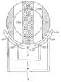
- FIG. 6a top view of reactor 200 showing both processing stations 301 and 302 , inner quartz tube 601 and outer quartz “peanut” 602 are shown.
- Side heaters 411are also peanut shaped, and are positioned inside outer quartz peanut shield 602 .
- the heating element of a resistive heatermay, in some embodiments, comprise a strip of electrically conductive material embedded within a matrix of a nonconductive material having a similar coefficient of thermal expansion, thus forming a monolithic structure. Further details of such a heater are described in a co-pending application titled “Apparatus and methods for resistively heating a thermal processing system,” filed Nov. 16, 2000, assigned to the assignee of the present application, and incorporated herein by reference.
- the active heating elementmay be a low resistivity trace of a ceramic material embedded within a higher resistivity ceramic material having similar properties of thermal expansion.
- the low resistivity materialmay be nitrogen doped silicon carbide, which has a resistance approximately 4 orders of magnitude lower than the un-doped silicon carbide matrix.
- the heaters that surround the process cavity, and the structures surrounding the heater systemmay comprise a chamber liner until ultimately reaching the chamber walls themselves.
- chamber liner 420Above shield 416 is chamber liner 420 , which protects the hardware that is positioned toward the interior of the processing chamber from contaminants diffusing out of chamber wall 421 , as well as protecting the chamber walls from the corrosive gasses used in the process cell. Shield 416 also provides thermal insulation for the process cavity, enhancing the temperature uniformity of the cavity, and insulating the chamber walls from high temperatures.
- the chamber wallsmay comprise aluminum, anodized aluminum, and stainless steel.
- Chamber liner 420comprises opaque quartz in this embodiment, so that infrared energy is confined to the processing chamber.
- the side walls 422 of the chambermay be water-cooled by flowing a cooling liquid, such as water, through the middle of the wall.
- the top and bottom chamber wallshave water cooling holes as well (not labeled).
- Side walls 422are protected by side quartz chamber liner 424 .
- the stainless steel bottom chamber walls 426is protected by quartz liner 425 .
- FIG. 8illustrates the symmetry between the two substrate processing regions of exemplary reactor 200 .
- FIG. 8emphasizes the concept that the principles of the present invention may be used to process two substrates simultaneously.
- the outer upper heater zone for the right-hand processing station 302is labeled 810 a in FIG. 8.
- Heating zone 810 a in FIG. 8is the right-hand analogy to left-hand heating zone 410 a in FIG. 4.
- the middle heating zone 810 b in FIG. 8is analogous to the heating zone 410 b in the left-hand side of reactor 200 . It will be appreciated that there are no side heating elements in the middle of FIG. 8, approximately at location 801 , because this heater is peanut shaped does not extend into the region between the two processing stations (see FIG. 6 as well).
- a bottom heater 813 , bottom shield 814 , and top shield 815 of the right-hand processing station 302is shown in FIG. 8.
- Embodiments of the present gas inject systemare in part responsible for achieving the desired thickness uniformity, resistivity uniformity, and control over the doping transition width that is achievable according to embodiments of the present reactor.
- plenum 429is arc-shaped in a plan view, and the tops of the five inject tubes 427 are just visible through their respective slits 430 in the plenum.
- the concept underlying plenum 429 and slits 430is to have a flow that is more spread out that would be achieved otherwise with five individual tubes. This is depicted schematically in FIG. 10A, where a gas stream 1001 spreads out into a fan shaped flow 1002 before passing through slit 430 .
- the fanforces the flow to go from a circular shape into a slotted, linear flow.
- the fanning-out nozzlemay be part of the quartz gas inject tube.
- the design of the gas inject systemwill be now be described to explain several advantageous features of this embodiment.
- the two outer gas inject tubesare fed from the same source, and are labeled “E” for “edge.”
- the next two gas tubesare labeled “M” for “middle.”
- the center tubeis labeled “C” for “center.”
- the gasesare plumbed such that there is independent control of the silicon concentration, dopant concentration, and carrier gas flow (the carrier gas may be hydrogen, and may be called “hydrogen mainstream”) for each of the three zones edge, middle, and center.
- the edge feedplenumizes (or splits) into the two edge jets, and that portion of the source flows over the edges of the wafer indicated (if a “snapshot” in time could be observed) in general by the cross-hatched regions 1101 in FIG. 11. Since the substrate is rotating, however, the region of the wafer covered by the two edge inject tubes fills the annulus outside the circle indicated by 1102 in FIG. 11. The regions supplied by the two middle inject tubes, at an instantaneous snapshot in time, is shown by the unhatched region 1103 of the substrate. Gases from the middle zone fan out to cover a zone that is neither edge nor center in character. The center jet covers the double cross hatched region 1104 , again ignoring the fact that the substrate is rotating. Of course, there will be a blending of the regions, even though the flows have been represented as being discrete and non-overlapping in FIG. 11.
- the ability to control the concentration of the dopant in the gas flows being delivered to each of the three zoneshas consequences with regard to epitaxial film properties, such as, for example, resistivity uniformity.
- the dopant concentrationmay be heavier than desired at the edges of the substrate due to the autodoping effect caused by dopant de-gassing from the backside of heavily doped wafers. If this is the case, the doping concentration in the gas flow being delivered to the edge zone 1101 may be reduced to compensate for the fact that the doping is high on the edge from the backside autodoping.
- Gasesare injected through tubes 427 , are directed by plenum slots 430 into process cavity 303 , then travel across the substrate, and are exhausted through ports 431 . As they are ejected from the slot 430 , they “bounce” off the lower, inner surface of hood 409 , and change direction from vertical to horizontal to flow across the process cavity toward the exhaust tubes. This re-direction of the flow is performed for a several reasons, one of which is to preheat the feedgas in preparation for its decomposition and subsequent reaction. A particular advantage of this strategy is apparent when silane is used a silicon source gas, but at the present time, epitaxial silicon depositions are commonly performed with chlorinated silanes, wherein trichlorosilane is perhaps the industry standard.
- the chlorine content of the silicon source gasaffects the growth rate of film according to the following pattern: for a given temperature, the higher the chlorine content, the slower the growth rate.
- the chlorine contentalso affects the transition temperature at which polycrystalline and single crystal silicon is grown. With silane as the source, epitaxial silicon films may be grown at temperatures as low as 900° C. At the other end of the extreme, reaction temperatures for the deposition of single crystal silicon from SiCl 4 must be kept above 1100° C.
- a disadvantage of depositing from silaneis that gas phase (homogeneous) nucleation is commonly observed, and such an event is undesirable since silicon aggregates may lead to particle contamination. Because of the potential advantages outweigh any disadvantages, what is needed is a reactor specifically designed to mitigate these problems such that it can be configured to deposit an epitaxial silicon film from silane. A discussion of the capability of the present reactor to epitaxially deposit silicon from silane will be reserved for later.
- Lamp-heated, conventional bell jar reactorsare often horizontal flow systems.
- the reactant gasesfirst pass over section 115 of the susceptor 103 before encountering any part of the substrate. This serves to pre-heat the gases.
- the pre-heating stepbegins the dissociation of the silicon containing component of the feedgas; otherwise, the gas stream will have progressed well over the substrate before any dissociation has begun. In this latter case, with no pre-heating of the gases, and where dissociation of the silicon containing gas has begun at too late a stage, the growth tends to be thicker on the downstream portions of the substrate, and poor thickness uniformity may result.
- a second problem experienced with conventional reactorsis that unreacted gases and reaction by-products are conducted into the exhaust lines, where they re-condense into a trichlorosilane-based liquid waste substance. In fact, a dangerous situation may arise because the resulting coatings may be pyrophoric.
- the efficiency of the reaction in a reactor similar to that of FIG. 1has been estimated to be about 5 to 10 percent, even with pre-heating, which means that a large majority of the reactant gases are being wasted as they condense on the walls of the exhaust lines.
- Embodiments of the present inventionpre-heat the gas without overheating it by, among other things, controlling the speed at which the feedgas is flowed through gas inject tubes 427 , and the volume of the carrier gas component.
- the feedgas streampicks up less heat the faster it is flowed through gas inject tube.
- Another technique for controlling the temperature of the reactant gases prior to their entry into the process cavity, in a less dynamic fashion,is by selection of the materials from which gas inject tubes 427 are fabricated.
- coarse control of the temperature of the feedgasmay be realized by choosing an appropriate material for the tube 427 .
- NOTEfor even less gas heating than clear quartz, a co-axial tube could be used with H2 in the outer annulus and the process gas in the inner tube
- a first choiceis clear quartz, which provides a relatively low level of heating due to the transmission of the majority of incoming radiation (emissivity ⁇ 0.15).
- a second choiceis opaque quartz, which partially absorbs radiation and, as a result, provides a higher level of heating.
- the yield of the reactionmay be influenced not only by the temperature of the reactant gases, but by the shape of the boundary layer as well.
- a showerhead designhaving gases directed perpendicularly toward the substrate, provides a more efficient use of the feedgas, in part because of the lack of any substantial boundary layer.
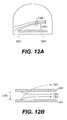
- the boundary layer of a conventional bell jar and direct flow reactormay be depicted as boundary layer 1201 in FIG. 12A.
- the boundary layercontinues to pull away from the substrate after it has been formed at location 1202 , and as the gases flow toward position 1203 .
- a competitionis induced within the boundary layer between the silicon containing gas molecules diffusing toward the surface of the substrate, and the HCl reaction products diffusing from the surface of the substrate back into gas stream 1204 .
- the bell jar reactors of FIG. 12Ahas a boundary layer 1201 that increases in thickness in going from position 1202 to 1203 , and consequently it becomes more and more difficult for the exchange to take place.
- Embodiments of the present inventionprovide the ability to vary the distance separating the two plates (susceptor 401 and hood 409 ). Typical separation distances range from about 0.25 to about 3 inches. The distance separating the susceptor and the hood will affect many properties, including, growth rate, thickness and resistivity uniformity, autodoping, and other doping characteristics, because for a given gas volume, the flow will be faster for a smaller process space.
- the ability to vary separation distance 1205can be used to provide additional control over processing properties. It is estimated that embodiments of the present reactor provide a reaction efficiency that is at least two times more efficient than a reactor of the type shown in FIG. 1.
- a carrier gas such as hydrogenmay be injected through a showerhead to control the temperature of the feedgas, and to dilute the concentration of the source-gas components.
- a showerhead designcould include a plenumized mainstream for gas temperature control over the wafer, plenumized silicon with H2, plenumized dopant with H2, and plenumized silicon and dopant with H2.
- the showerheadcould also provide localized silicon, dopant, silicon and dopant injection where the showerhead would be used to “fan out” the direct inject point to a larger diametrical area over the wafer whose area would be dependent on the showerhead hole sizes and overall flow from the direct inject source above the showerhead.
- the pyrometersare not spaced as closely together in the center region of the substrate because the edge heaters do not have as much of an effect in the center region as they do at the edge.
- the last optical pyrometer that looks at the edge of the susceptoris labeled 601 .
- the temperature measuring devicesmay be used to inject gases as illustrated in FIG. 15.
- lightpipe housing 1501is used to receive information from the upper edge heater 41 a .
- lightpipe housing 1502looks at the lower edge heater 411 b.
- a typical purge gasmay be an inert gas, a noble gas, or a carrier gas such as hydrogen.
- the type of gasis not important, as long as there is a flux of any gas to prevent an undesired deposition on the tip of the fiber.
- the volume of the gas required to keep the system cleanis minimal, and may range from about 100-500 cubic centimeters per minute, with 100-200 cubic centimeters per minute being typical.
- the purge gasmay be exhausted from the chamber using exhaust tubes 431 . In some embodiments, such as the exemplary embodiment of FIG. 13, each of the optical pyrometers 1301 and 1302 exhaust their gases over the substrate.
- the purge gasmay be used to fine-tune resistivity uniformity by delivering a dopant supply gas to dopant-poor regions of the growing epitaxial layer.
- the dopant concentrationmay be low in certain regions due to, for example, depletion or outgassing mechanisms.
- a dopant supply gasmay be injected through the sheath of an optical pyrometer.
- An example a particularly effective use of this techniqueis the injection of a dopant carrier gas through a central optical pyrometer 1303 to compensate for the lack of dopant at the center of the layer that may occur at location 1008 (see FIG. 10B).
- the purge gas of an optical pyrometermay, according to embodiments of the present invention, be used to keep the tip of the optical fiber clean, and locally effect the resistivity of the epitaxial layer, among other things.
Landscapes
- Chemical & Material Sciences (AREA)
- Engineering & Computer Science (AREA)
- Organic Chemistry (AREA)
- General Chemical & Material Sciences (AREA)
- Chemical Kinetics & Catalysis (AREA)
- Materials Engineering (AREA)
- Metallurgy (AREA)
- Physics & Mathematics (AREA)
- Mechanical Engineering (AREA)
- Condensed Matter Physics & Semiconductors (AREA)
- General Physics & Mathematics (AREA)
- Manufacturing & Machinery (AREA)
- Computer Hardware Design (AREA)
- Microelectronics & Electronic Packaging (AREA)
- Power Engineering (AREA)
- Crystallography & Structural Chemistry (AREA)
- Fluid Mechanics (AREA)
- Chemical Vapour Deposition (AREA)
Abstract
Description
- The present application is based on and claims priority to a provisional application filed on Apr. 12, 2001, having U.S. Serial No. 60/283,541.[0001]
- The present invention relates in general to the processing of semiconductor substrates, and more particularly, to improved systems and methods for epitaxially depositing films onto a semiconductor substrate.[0002]
- Processes utilizing epitaxial deposition generally involve the growth of one or more layers or films onto a semiconductor substrate. The growth of these layers is carefully controlled by the underlying processes and equipment to produce layers having the desired physical, electrical and mechanical characteristics. These characteristics typically include, for example, the growth rate and thickness of the epitaxial layer, resistivity, dopant concentration, doping transition width, defect density, level of metal and particle contamination, and slip. Because these characteristics are highly dependent upon the operating conditions (e.g., temperature, gas flow rate and concentration of process gases) under which the epitaxial layers are grown, the underlying processes and equipment must maintain precise control over these operating conditions in order to produce epitaxial layers having uniform characteristics over the entire surface of the semiconductor substrate. Maintaining the required level of control, however, has proven increasingly difficult to achieve due to the recent transition from 200 mm to 300 mm fabrication processes, the tighter process specifications imposed by many semiconductor manufacturers and the higher throughput requirements (the number of substrates processed per unit of time) necessary for cost-effective manufacturing. In light of these increased processing demands, maintaining the necessary level of control while simultaneously satisfying throughput requirements, has proven increasingly difficult to achieve using conventional epitaxial deposition approaches.[0003]
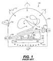
- Referring to FIG. 1, an exemplary reactor for performing epitaxial deposition in accordance with an existing approach is illustrated generally at[0004]100. The exemplary reactor consists of a quartz bell-
shaped jar 101 which encloses asemiconductor substrate 102 and isolates thesubstrate 102 from outside contaminants. The bell-shaped jar 101 also encloses asusceptor 103 which is used to support and rotate thesemiconductor substrate 102 during processing. The process gases used to deposit epitaxial layers are injected into the reactor through agas inlet port 104 and are exhausted out of the reactor through anexhaust port 110 located at the opposite end of the reactor. In order to heat both thesemiconductor substrate 102 and process gases to operating temperature, a number ofquartz halogen lamps 112 are positioned around the upper portion of the bell-shaped jar 101 to radiate energy into the reactor through the transparent walls of the bell-shaped jar 101. Anoptical pyrometer 113 located above a small window114 in the reactor wall detects the temperature of the reactor. Theoptical pyrometer 113 relays the temperature measurements to appropriate lamp control circuitry (not shown) which then increases or decreases the output of thehalogen lamps 112 in response to the detected temperature of the reactor. - In operation, the exemplary reactor of FIG. 1 deposits an epitaxial layer on the[0005]
semiconductor substrate 102 by injecting process gases into the bell-shaped jar 101 via thegas inlet port 104. These process gases typically include a silicon source gas, such as silicon tetrachloride (SiCl4), trichlorosilane (SiHCl3), and dichlorosilane (SiH2Cl2), and a carrier gas, such as hydrogen. The process gases may also include n-type dopants or p-type dopants, which may be provided by precursor gases such as arsine (AsH3), and phophine (PH3) or diborane (B2H6). Thegas inlet port 104 directs agas stream 105 of the process gases horizontally toward thesemiconductor substrate 102. As thegas stream 105 approaches and passes over thesemiconductor substrate 102, the relatively large volume of the bell-shaped jar 101 causes thegas stream 105 to split into alaminar flow 106, which flows across the surface of thesubstrate 102, and the naturally circulatingflow 107 which fills the upper portion of the bell-shaped jar 101. The flow can be laminar or turbulent, depending on the temperature gradient and characteristic length (from susceptor surface to top surface of chamber enclosure). Aboundary layer 108 is also produced above the surface of thesemiconductor substrate 102 due to the velocity gradient between thelaminar flow 106 and the relatively stationary (although rotating)semiconductor substrate 102. - As the laminar flow passes over the[0006]
semiconductor substrate 102, some of reactants diffuse through theboundary layer 108 to adsorb on the surface ofsemiconductor substrate 102. Once adsorbed, thereactants 115 undergo surface diffusion to find anappropriate lattice site 116 on the growing single crystal film. This surface diffusion step requires energy, and is an important factor that determines the quality of the resulting epitaxial layer. If the surface energy is insufficient for a reactant to become accommodated at a lattice site before additional atoms have accumulated over it, undesirable defects in the crystal lattice will occur. Thereactants 115 also react chemically with the surface of thesemiconductor substrate 102 to form by-products 117, which desorb from the surface and diffuse through theboundary layer 108 back into thelaminar flow 106 and are then removed from the reactor through theexhaust port 110. - Conventional epitaxial reactors, such as the reactor illustrated in FIG. 1, suffer from several deficiencies which may prevent these reactors from providing an effective and cost-efficient solution for various applications. One problem is that the bell-[0007]
shaped jar 101 has a relatively large volume which inhibits the ability of the reactor to precisely control the processing temperature of thesemiconductor substrate 102 and the process gases. As mentioned previously, the operating temperature of thesemiconductor substrate 102 and process gases is a critical factor in achieving the desired physical, electrical and mechanical characteristics. If the temperature is too low, the reactants will have insufficient energy to become accommodated at an appropriate lattice site, which may result in an increase in the defect density within the crystal lattice. If the temperature is too high, in the case of SiH4or Si2H6, silicon molecules will bond together to form silicon aggregates in the vapor phase. These silicon aggregates can then fall to the surface of thesubstrate 102 and interfere with single crystal growth. Although it would be desirable to reduce the volume of the bell-shaped jar 101, the ability to do so may be limited by structural integrity constraints of the reactor. - Another problem relates to the ability of existing reactors to control the flow and concentration of process gases over the surface the[0008]
semiconductor substrate 102. As thelaminar flow 106 of FIG. 1 passes over thesemiconductor substrate 102, reactants within the process gases will be steadily depleted so that thelaminar flow 106 will have a lower concentration of reactants near the exhaust port110 than near thegas inlet port 104. Although the affects of depleted reactant concentration can be reduced for the perimeter of thesemiconductor substrate 102 by rotating thesemiconductor substrate 102 during processing, the depleted reactant concentration over the inner portion of the semiconductor substrate are not adequately addressed by the gas flow system of FIG. 1. Consequently, thesemiconductor substrate 102 will have a greater thickness and a lower resistivity around the peripheral portion of thesemiconductor substrate 102 than the inner portion of thesemiconductor substrate 102. - Yet another problem involves the potential for build-up of a low quality silicon film on the walls of the bell-[0009]
shaped jar 101. Designers of so-called “cold-wall” reactors typically expend substantial effort to maintain the temperature of reactant gases high enough for reaction to occur, and, simultaneously maintain the temperature of bell-shaped jar 101 low enough to avoid the deposition of an amorphous, low quality silicon film on its walls. If the walls get too hot, however, silicon molecules will adhere not only to thesemiconductor substrate 102, but also form a thin film on the quartz walls of the reactor. This undesired, low quality film can tint the bell-shaped jar 101 and cause a variety of problems. Because the amorphous silicon adheres poorly to the quartz bell-shaped jar 101, and because there is mismatch in thermal expansion coefficients of silicon and quartz, the silicon has a tendency to flake off the quartz walls when the reactor is cooled. The amorphous silicon can also flake off the quartz walls during processing and fall onto thesemiconductor substrate 102 thereby producing particulate contamination. The tinted bell-shaped jar 101 also reduces the amount of energy that can pass through it from thehalogen lamps 112. Additionally, amorphous silicon may coat window114, which causesoptical pyrometer 113 to receive less light energy than it otherwise would have. Theoptical pyrometer 113 will then erroneously detect that the wafer temperature is cooler than it should be, and will instruct thehalogen lamps 112 to deliver more energy, leading to even more unwanted deposition on the bell-shaped jar 112. As a result, it is frequently necessary to etch these deposits off of the bell-shaped jar with HCl after each semiconductor substrate is processed, which decreases the throughput of the reactor. - Therefore, in light of the deficiencies of the prior art and the increasing importance of epitaxial deposition in a variety of integrated circuit technologies, such as bipolar junction transistor (BJT) and complimentary metal oxide semiconductor (CMOS) technologies, there is a need for improved systems and methods for depositing epitaxial layers on a semiconductor substrate.[0010]
- Embodiments of the present invention provide improved systems and methods for increasing the quality and throughput of semiconductor substrates. In accordance with aspects of the present invention, an epitaxial reactor is configured to include a hot wall process cavity enclosed by a heater system, a thermal insulation system, and chamber walls. One of the walls enclosing the process cavity includes a slit through which a semiconductor substrate may be inserted within, and extracted out of, the process cavity without requiring cooling of the process chamber. The walls of the process cavity may also comprise a material, such as quartz or silicon carbide, that has thermal properties substantially similar that of the semiconductor substrate. In this context, the walls of the process chamber may be heated to a temperature within 200° C. of the semiconductor substrate, particularly to a temperature within 100° C. of the semiconductor substrate, while the semiconductor substrate is being heated. In one embodiment, for instance, the walls of the process chamber may be heated to approximately the processing temperature of the semiconductor substrate.[0011]
- By using a hot wall processing chamber, during the formation of layers containing silicon, molecules adhering to the surface of the walls form metallic silicon instead of amorphous silicon. This metallic silicon is more stable than the amorphous silicon film that typically forms on the walls of cold wall reactors, thereby enabling a reactor incorporating the principles of the present invention to successively process multiple semiconductor substrates without requiring cleaning of the reactor walls between each processing cycle. As a result, embodiments of the present invention may be used to provide high throughput epitaxial deposition within a stable thermal environment and may avoid the use of complex and expensive lamp systems. The process cavity may also have a relatively small volume which restricts the thickness of the boundary layer and allows a more efficient exchange of reactants with reaction by-products through the boundary layer to the substrate.[0012]
- The reactor may also include a gas supply system that injects process gases into the process chamber through a plurality of gas inlet ports. The flow rate and/or concentration of each of the plurality of inlet ports may be controlled individually or in groups to selectively control the flow of process gases over, for example, the edge, middle and center zones of the semiconductor substrate. The gas supply system may also control the flow rate of each of a plurality of exhaust ports to selectively control the flow of process gases over the semiconductor substrate, either alone or combination with the selective control of the gas inlet ports.[0013]
- Alternatively, the gas flow system may incorporate a shower head in an upper portion of the process chamber to direct process gases down towards the surface of the substrate, thereby reducing the boundary layer. Another alternative for reducing the boundary layer involves shaping the upper wall of the process cavity to form a recessed or bowl-shaped portion within the process cavity. The gas supply system may further include additional methods of delivering gas to the process cavity, such as through apertures used for temperature measurement devices. Also, because the exemplary reactor includes a hot wall process cavity, and because the heat source of the exemplary reactor is internal to the processing chamber and is not transmitted through a clear quartz jar, this reactor chamber may be configured to use efficiently and effectively use silane as a silicon source gas.[0014]
- In one embodiment of the present invention, the gas inlets that are used to feed gas into the chamber include a longitudinal section and a lateral section. The longitudinal section can extend into the chamber from the bottom of the chamber or from the top of the chamber. The lateral section, on the other hand, can be configured to direct the flow of gases over the surface of the wafer. In this arrangement, the gases flow in generally a vertical direction into the chamber and then are directed horizontally across the wafer. Further, the lateral section can be configured to plenumize the flow of gases over the surface of the wafer.[0015]
- In one particular embodiment, the longitudinal section of the gas inlets can be positioned adjacent to a heating device, such as an electrical resistance heater that is used to heat the chamber. In this manner, the gases flowing through the gas inlets are preheated prior to being exposed to the wafer.[0016]
- The lateral sections of each of the gas inlets can be in communication with a support ring defining a common plenum. The plenum can be used to spread the gases over the entire surface of the wafer. Similarly, this system can include an exhaust system positioned on the opposite side of the wafer from the gas inlets. The exhaust system can include an exhaust ring for exhausting gases from the chamber. The exhaust ring can be in communication with multiple gas exhaust outlets. In one embodiment, the system can include at least five gas inlets and at least five gas outlets.[0017]
- The processing chamber can include a heating device for heating the chamber and any semiconductor substrates contained within the chamber. In one embodiment, the heating device can comprise a cage-like heating system. The cage-like heating system can include a top resistive heater, a bottom resistive heater, and at least one side resistive heater. In one embodiment, the longitudinal sections of the gas inlets can be positioned adjacent to at least one of the resistive heaters. In this manner, gases are preheated prior to contacting the semiconductor wafer.[0018]
- In another embodiment of the present invention, the lift pin mechanism that raises a substrate off a susceptor is capable of rotating with the susceptor during processing. This ability to rotate the lift pins with the susceptor eliminates the difficulty and risk of lift pin breakage associated with stopping the rotation of the susceptor so that the lift pins are in alignment relative to corresponding holes in the susceptor. This embodiment also increases throughput by reducing the amount of time necessary to extract substrates from the process cavity due to avoidance of the time spent homing the rotation to normally stationary pins.[0019]
- These and other features and advantages of the present invention will become more apparent to those skilled in the art from the following detailed description in conjunction with the appended drawings in which:[0020]
- FIG. 1 illustrates an exemplary reactor for depositing epitaxial layers in accordance with an existing approach;[0021]
- FIG. 2 illustrates an exemplary reactor system in which the principles of the present invention may be advantageously practiced;[0022]
- FIG. 3 illustrates a side-view of an exemplary reactor, with the interior of the left-hand portion exposed;[0023]
- FIG. 4 illustrates an enlarged side-view of the interior of the left-hand portion of the exemplary reactor;[0024]
- FIG. 5 illustrates an exemplary heating system which incorporates the principles of the present invention;[0025]
- FIG. 6 illustrates a top plan view of an exemplary processing chamber, showing details of the edge heaters, side quartz liners, gas inject tubes, and gas exhaust tubes;[0026]
- FIG. 7 illustrates an exemplary monolithic plate heater in accordance with the principles of the present invention;[0027]
- FIG. 8 illustrates a three-dimensional view of the reactor with both processing stations exposed, and shows the symmetry of the gas inject and exhaust systems;[0028]
- FIG. 9 illustrates a top, plan view of the gas inject tubes and gas exhaust tubes;[0029]
- FIG. 10A illustrates how the gas from a gas inject tube may be spread out to achieve a more uniform distribution;[0030]
- FIG. 10B illustrates a schematic illustration how the dopant concentration may be depleted from the feedgas stream;[0031]
- FIG. 11 illustrates how the gas inject system may be configured to achieve a desired thickness and uniformity resistivity;[0032]
- FIG. 12A illustrates, schematically, a thick gas flow boundary layer in a conventional epitaxial reactor;[0033]
- FIG. 12B illustrates, schematically, a thin gas flow boundary layer according to embodiments of the present invention, where gases are confined to a narrow space between two parallel plates;[0034]
- FIG. 13 illustrates an exemplary distribution of temperature measuring devices that take readings from the top of the substrate and, in some embodiments, also inject gases to adjust thickness and resistivity uniformity;[0035]
- FIG. 14A illustrates a top, plan view of two, intersecting arrays of temperature measuring devices;[0036]
- FIG. 14B illustrates a side view of how temperature measurement devices along an array may be distributed, as a function of distance, from the center to the edge of a substrate;[0037]
- FIG. 15 illustrates a cross-sectional view of an exemplary reactor in which a temperature measuring device may be used to inject a purge gas to a processing chamber; and[0038]
- FIG. 16 illustrates an exemplary configuration of an optical fiber and sheath in which a purge gas may flow inside the sheath but outside the optical fiber.[0039]
- Aspects of the present invention provide improved systems and methods for processing semiconductor substrates. An exemplary embodiment of the present invention provides a stable, hot-walled thermal environment for epitaxial or potentially any other thermal CVD deposition on semiconductor wafers. An insulated processing cavity is formed from opaque quartz walls and a rotating susceptor and may enclose or be surrounded by a resistive heating system. The walls thermally insulate the processing cavity from the cooler surrounding environment and provide a relatively uniform and stable thermal processing environment. The processing environment may also be maintained at vacuum pressure to increase insulation and the stability of the thermal environment. Wafers are inserted through a narrow slot into the processing environment and onto pins which lower the wafer on the heated susceptor. The wafer is rotated on a susceptor and a silicon deposing gas is flowed across the surface of the wafer. The processing cavity is relatively compact which improves process efficiency and control. While deposits may form on the hot walls of the processing cavity, the deposits tend to be metallic silicon which is relatively stable. After processing, the wafer is raised on the pins and removed from the cavity. The processing cavity may be enclosed within the processing chamber that has an aligned slot or port, so the wafer may be inserted into and removed from the processing cavity and chamber laterally in a single motion along the same horizontal plane. The processing cavity may be maintained at a high temperature during both insertion and removal. Thus, a very high throughput may be attained with a stable thermal environment and without requiring complex lamp systems or heating up and cooling down a cold-wall processing environment for each wafer that is processed.[0040]
- An additional advantage of this embodiment is its ability to process a variety of different sizes and shapes of semiconductor substrates. In a cold-wall lamp system, the lamps and the temperature control system may need to be substantially reconfigured for substrates of different sizes, but the stable thermal environment of the above embodiment allows different sizes to be accommodated relatively easily. Although the reactor may be specifically designed to process 300 mm diameter silicon wafers, it may permit 200 mm, 150 mm, and 125 mm silicon wafers to be processed as well. The ability to process a variety of different sized wafers may reduce the cost of ownership. The reactor may act as a “bridge tool,” bridging a manufacturer's transition from one sized substrate to another. A chip manufacturing facility that is not yet ready to transition to 300 mm substrates, for example, may still use the tool to process 200 mm substrates. Once the size conversion is ultimately implemented, the manufacturer may avoid having to purchase an entirely new system.[0041]
- Referring to FIG. 2, an exemplary system in which the principles of the present invention may be advantageously practiced is illustrated. The structural parts of the exemplary system include processing chamber for enclosing and a process cavity, where the process cavity has a susceptor (which could also be described as a substrate support plate) and a hood forming the bottom and top of the cavity, respectively. Heaters enclose the process cavity at the top and bottom, and along the sides at certain locations, depending on how many substrates are being processed and the desired heat transfer characteristics. Outside the heaters are chamber liners that provide thermal insulation and protection from contamination from the chamber walls, and finally, the chamber walls themselves. Within the heater-cage structure, and adjacent to and below the susceptor, is positioned a lift pin support plate assembly responsible for raising the substrate off the susceptor. Also enclosed in this region is a central post (and related hardware) for raising and lowering the susceptor into positions in the process cavity, and adjacent to the transfer port. Process gases are injected into the process cavity and exhausted out of process cavity by a gas supply system. In light of this overview of the exemplary system, a more detailed description of the components of the exemplary system, rotating lift pin support structure, heating system and gas inject system will now be provided.[0042]
- As illustrated in FIG. 2, the exemplary system includes an epitaxial deposition reactor, depicted generally at[0043]200, having a
front plate 201 that may be mated with the robotic wafer transfer chamber of asubstrate transport system 207. An exemplary substrate transport system is the Aspen III system available from Mattson Technology, Inc. The horizontal slit202 in the middle offront plate 201 is the port through which wafers are transferred into and out ofreactor 200 from the transfer chamber of thewafer handling system 207. Thereactor 200 also includeselectrical feedthroughs 203 at the top of thereactor 200, andsusceptor manipulating equipment 204 at the bottom of the chamber.Gas supply inlets 205 are provide at a bottom portion of the chamber. The processing chamber further comprises a process cavity surrounded by at least one layer of insulating shields, which in turn are surrounded by the processing chamber walls. - The[0044]
epitaxial reactor 200 is further coupled to agas supply system 210 for receiving process gases into thereactor 200, a pumping system oratmospheric exhaust line 208 for exhausting gases from thereactor 200, awafer transport system 207 for inserting and removing wafers, amechanical system 209 for manipulating the susceptor, and acontrol system 212 for controlling and monitoring the operation of thereactor 200 and the foregoing subsystems as well as peripheral equipment such as optical pyrometers and other temperature measuring devices of thetemperature control system 210. - Referring to FIG. 3, the exemplary reactor of FIG. 2 is illustrated in cross-section, where[0045]
front plate 201 has been removed from the left-hand portion 301 of thereactor 200 to reveal the interior of left-hand portion 301. The exposed, left-hand portion 301 is essentially mirrored on the right-hand side 302, which is still covered byfront plate 201. - Referring now to FIG. 4, an enlarged view of the process cavity, depicted generally at[0046]303 in FIG. 3, is illustrated. The
process cavity 303 containssubstrate holder 401, which has aslight recess 402 to help securely maintain the position of the substrate (not shown) on thesubstrate holder 401 during processing. The size and shape of therecess 402 may be configured, for example, so that the edge of a 300 mm (12 inch) silicon wafer rests againstrecess 402.Substrate holder 401 may comprise solid silicon carbide, silicon carbide coated graphite or another material that minimizes contaminant flow from thesubstrate holder 401 and that has compatible thermal characteristics with the semiconductor wafer.Substrate holder 401 may be referred to as a susceptor. - [0047]
Substrate holder 401 is in turn supported bysupport plate 403 which may be composed of a material, such as quartz. Quartz offers advantages for this particular application because quartz can be fabricated into a part having a low impurity content, very low CTE, and because quartz is generally less expensive than silicon carbide. Thesupport plate 403 may be easily bonded to centerpost 404. Liftpin support plate 405 may also be fabricated from quartz, and hasreceptacles 406 for lift pins407. Lift pins407 penetrate all the way up throughsupport plate 403 to terminate insidesubstrate holder 401, without exiting beyond the top surface of thesubstrate holder 401. Lift pins407 are said to be “nested” withinsubstrate holder 401. Liftpin support plate 405 is attached to outercenter post tube 408, which coaxially surroundscenter post 404.Center post 404 also supports and registers the support plate onnub 409 in a central location (relative to the center of the substrate). - There are advantages to having the lift pins[0048]407 nested in a respective holes in the
substrate holder 401, and further advantages to having a coaxial assembly of thecenter post 404 and the outercenter post tube 408 in a centrally located position relative to liftpin support plate 405. Having the lift pins407 rotate as the substrate rotates during processing offers advantages with regard to throughput by eliminating the need to decelerate the substrate holder and slowly rotate the substrate holder so that the lift pins perfectly align with corresponding holes on the bottom of the substrate holder before actuating pins to lift wafer off ofsusceptor 401. - The exemplary embodiment of FIG. 4 provides lift[0049]
pin support plate 405 withreceptacles 406, to which lift pins407 are attached, and keyed to centerpost 404 in a rotation housing. With such a design, the pins are constantly aligned with the holes in the substrate holder, even during rotation of the substrate during processing. Thermal losses are minimized as well because the lift pins continuously aligned with, and are partially contained within, their respective holes insubstrate support plate 403. Because the lift pins407 rotate withsubstrate support plate 403 during processing, the lift pins407 are positioned within the holes of thesubstrate support plate 403 the majority of the time. The outercenter post tube 408 is keyed with thecenter post 404 in the rotation housing below the processing chamber (at a position roughly indicated byreference numeral 204 in FIG. 2), and the hardware associated with and responsible for lifting the wafer off thesubstrate support plate 403 rotate together, with the result that the lift pins407 are always aligned with their respective holes insubstrate holder 401 andsupport plate 403. By plugging these “thermal gaps” (the holes in the plate), heat loss from the wafer is reduced, and the thermal profile presented to the wafer from thesubstrate support plate 403 is more uniform. This reduces heat loss from the wafer. When it is time to unload the wafer, the wafer is first lifted offsubstrate holder 401 by the lift pins407. Because the lift pins407 are already aligned with the holes, they need only be raised enough to provide a gap for the robotic transfer arm, such as approximately ½ to 1″ above the top surface of401. - The support pin structure of FIG. 4 avoids the mechanical risks of having a lift pin support plate stationary while a substrate holder and support plate rotate. This avoids the risks of raising the lift pin support and having the lift pins misaligned. If the lift pins should break, the reactor must be opened and at least in a part disassembled to replace the pins, resulting in the loss of a significant amount of processing time. The exemplary support pin structure avoids the risk of temperature non-uniformity caused by having open (unblocked) holes in the support plate supporting the wafer, and the thermal risk of having thermal shock to the wafer if the lift pins contacting the wafer are at a different temperature from the wafer.[0050]
- It should be emphasized that this concept of having rotating lift pins are not limited to epitaxial processing systems. Rather, this approach may be used in various types of semiconductor processing equipment as well, such as rapid thermal processing (RTP) and chemical vapor deposition (CVD) reactors and other systems using pins or rotating supports.[0051]
- Referring to FIG. 4, the top of the process cavity is provided by[0052]
hood 409. The process cavity created bysusceptor 401 at the bottom, and byhood 409 at the top, serves to confine reactant gases to the process cavity for processing of the semiconductor substrate. - Working outward from the process cavity (and the susceptor raising mechanisms associated with the lift pins) is the heating system. The heating system may comprise a cage-like structure that essentially encloses the process cavity (and susceptor lift mechanism). Referring to FIG. 4, a top heater[0053]410 may be positioned above
hood 409. Since this heater is being viewed in cross-section, the heating element may pass into and out of the plane of FIG. 4, and thus the heating element appears as a number of discrete members in FIG. 4. It should be noted that top heater410 may be configured with multiple heaters to form multiple heating zones. In the embodiment of FIG. 4, top heater410 is configured with an inner zone and an outer zone, although other configurations are contemplated and embraced by the present invention. The outermost four rectangles at the far right and far left-hand sides of the top heater410 comprise anouter heating zone 410a.Each of the approximately nineteen rectangles in the middle (only one of which has been labeled) comprise aninner zone 410b. - The heating system may also include side heating components. For example, the reactor may include a side heater having a[0054]
top element 411aand abottom element 411b. Alternatively, top and bottomside heating elements reference numeral 412 in FIG. 4, which points to the port through which the substrate is loaded and unloaded from the processing chamber. In the exemplary reactor of FIG. 4, a bottom heater comprising a single zone heater is labeled413. Of course, the bottom heater may have multiple zones as well. - For further clarification, the top, bottom, and side heating elements are shown in FIG. 5 as though they had been extracted as a single unit from the processing chamber. Also shown in FIG. 5 is the[0055]
substrate holder 401 and thesupport plate 403 underneath it,hood 409 forming the top of the process cavity, andcenter post 404. This FIG. 5 emphasizes the point that, in some embodiments, the heater system may comprise a cage-like structure that surroundsprocess cavity 303, and that by doing so, an isothermal environment is achieved giving a desired effect of no heat flow through, and excellent heating uniformity of the substrate. - It should be noted in FIG. 4 that each heating element, such as[0056]
bottom heater 413, may comprise a silicon carbide coated graphite heating element enclosed in anlower shield 414 and anupper shield 415. Each of the shields may also comprise silicon carbide coated graphite, but the graphite core of the shield is not resistively heated as it is in the case of the heating element. These shields (synonymously called “enclosures”) serve several purposes. They even out temperature non-uniformities from the regions adjacent to heating trace and the spaces between, generating better temperature uniformity adjacent to the heater as the heat is radiated up into the cavity. They also encapsulate the heating elements to prevent them from potentially being exposed to oxygen. A third purpose is to protect the heating elements in the event there are cracks in silicon carbide layer coating the graphite core. This prevents impurities in the graphite from reaching the process cavity. - [0057]
Top heaters top shield 416 andbottom shield 417. The side heaters may be enclosed by shields as well, but the shields do not necessarily have to be silicon carbide coated graphite. For example,side heaters 411 may be enclosed in quartz in one embodiment. - Referring to FIG. 6, a top view of[0058]
reactor 200 showing both processingstations inner quartz tube 601 and outer quartz “peanut”602 are shown. There is aninner quartz tube 601 surrounding each of the processing stations, one on the left and one on the right. There is only one peanut shapedouter quartz shield 602 in this embodiment, such thatshield 602 surrounds both processing stations.Side heaters 411 are also peanut shaped, and are positioned inside outerquartz peanut shield 602. - Referring back to FIG. 4, top side[0059]
heater support piece 418 lies between the twoside heaters Support piece 418 allows the upper heater to rest on the lower heater without being in electrical contact. It maintains a constant distance of separation between the two heaters and supports the upper heater. The lower heater is supported by itsown support piece 419. These side heater support pieces may take on a variety of shapes, depending on the geometry of the reactor, and in case the support pieces have a substantially peanut shaped configuration, just like the side heaters themselves. - The heating element of a resistive heater may, in some embodiments, comprise a strip of electrically conductive material embedded within a matrix of a nonconductive material having a similar coefficient of thermal expansion, thus forming a monolithic structure. Further details of such a heater are described in a co-pending application titled “Apparatus and methods for resistively heating a thermal processing system,” filed Nov. 16, 2000, assigned to the assignee of the present application, and incorporated herein by reference. The active heating element may be a low resistivity trace of a ceramic material embedded within a higher resistivity ceramic material having similar properties of thermal expansion. In certain embodiments, the low resistivity material may be nitrogen doped silicon carbide, which has a resistance approximately 4 orders of magnitude lower than the un-doped silicon carbide matrix.[0060]
- An exemplary monolithic plate heater is illustrated in FIG. 7. As with the conventional silicon carbide coated graphite heaters, a monolithic plate heater can have multiple zones as shown by[0061]
inner zone heater 701 andouter zone heater 702 in FIG. 7. Each zone has its own connector terminals shown as703 and704, respectively. - The heaters that surround the process cavity, and the structures surrounding the heater system may comprise a chamber liner until ultimately reaching the chamber walls themselves. Above[0062]
shield 416 ischamber liner 420, which protects the hardware that is positioned toward the interior of the processing chamber from contaminants diffusing out of chamber wall421, as well as protecting the chamber walls from the corrosive gasses used in the process cell.Shield 416 also provides thermal insulation for the process cavity, enhancing the temperature uniformity of the cavity, and insulating the chamber walls from high temperatures. The chamber walls may comprise aluminum, anodized aluminum, and stainless steel.Chamber liner 420 comprises opaque quartz in this embodiment, so that infrared energy is confined to the processing chamber. - The[0063]
side walls 422 of the chamber may be water-cooled by flowing a cooling liquid, such as water, through the middle of the wall. The top and bottom chamber walls have water cooling holes as well (not labeled).Side walls 422 are protected by sidequartz chamber liner 424. The stainless steelbottom chamber walls 426 is protected byquartz liner 425. - FIG. 8 illustrates the symmetry between the two substrate processing regions of[0064]
exemplary reactor 200. FIG. 8 emphasizes the concept that the principles of the present invention may be used to process two substrates simultaneously. The outer upper heater zone for the right-hand processing station 302 is labeled810ain FIG. 8.Heating zone 810ain FIG. 8 is the right-hand analogy to left-hand heating zone 410ain FIG. 4. Themiddle heating zone 810bin FIG. 8 is analogous to theheating zone 410bin the left-hand side ofreactor 200. It will be appreciated that there are no side heating elements in the middle of FIG. 8, approximately atlocation 801, because this heater is peanut shaped does not extend into the region between the two processing stations (see FIG. 6 as well). Equivalently, abottom heater 813,bottom shield 814, andtop shield 815 of the right-hand processing station 302 is shown in FIG. 8. - Next, the gas inject system will be described. Embodiments of the present gas inject system are in part responsible for achieving the desired thickness uniformity, resistivity uniformity, and control over the doping transition width that is achievable according to embodiments of the present reactor.[0065]
- Referring again to FIG. 4, a gas inject[0066]
tube 427 is shown configured to deliver gas vertically through the bottom of thechamber 426 up into theprocess space 303. In one embodiment of the present invention, there are five of these gas injection tubes (with one set o tubes for each side,301 and302). Although FIG. 4 is a cross section of the processing chamber, three other gas inject tubes are shown in FIG. 4 in a “quasi three-dimensional” view of the reactor. The cross-section of FIG. 4 passes through the gas injection tube on the far left, and may be used to illustrate how the gas injection tubes “plenumize” the gas. The term “plenumize” refers to the spreading of a gas flow in a desired manner by flowing the gas through a plenum. A plenum is a device (which may be a manifold) that acts to restrict the flow of the gas such that the gas flow is higher on the upstream side of the plenum, and in doing so the gas stream is shaped into a desired flow pattern. - The process gases flow up through[0067]
tube 427, and pass through gas injectsupport ring 428. Gas injectsupport ring 428 rests on quartzinner support tube 601.Inner support tube 601 provides mechanical support for gas injectsupport ring 428, but it also “nests” (or houses) the circular shape of the quartz tube so that it is registered to a particular position. Gas injectsupport ring 428, in turn, supports the gas injectplenum 429, into which the gases feed fromgas injection tube 427. The gases then flow throughplenum slot 430 before being redirected from a vertical to a horizontal flow across the substrate.Plenum slot 430 also serves to maintain zonal control of both concentration and flow through each of the five inlet tubes. The gases are “plenumized” byplenum 429, and are spread out into a linear fan across the substrate. This concept may be seen better in FIGS. 9 and 10. - Referring to FIG. 9,[0068]
plenum 429 is arc-shaped in a plan view, and the tops of the five injecttubes 427 are just visible through theirrespective slits 430 in the plenum. Again, the conceptunderlying plenum 429 and slits430 is to have a flow that is more spread out that would be achieved otherwise with five individual tubes. This is depicted schematically in FIG. 10A, where a gas stream1001 spreads out into a fan shaped flow1002 before passing throughslit 430. This results in a wider coverage over the substrate, having an exemplary width1003, rather than the smaller width1004 that would have occurred if gas stream1001 had been confined to a flow having the same diameter astube 427 at location1005. The fan forces the flow to go from a circular shape into a slotted, linear flow. In another embodiment, the fanning-out nozzle may be part of the quartz gas inject tube. - There are five gas inject[0069]
tubes 427 in this embodiment, but the number could range from about 1 to 9. Five inject tubes may be used, particularly with 300 mm substrates, because of the manner in which the gases spread out over the substrate, and because of the ability to control dopant, silicon, and mainstream gas concentrations over different regions of the substrate, and hence effect resistivity, thickness, and overall uniformity respectively. - Referring to FIG. 11, the design of the gas inject system will be now be described to explain several advantageous features of this embodiment. The two outer gas inject tubes are fed from the same source, and are labeled “E” for “edge.” Working inward from the edges toward the center, the next two gas tubes are labeled “M” for “middle.” Finally, the center tube is labeled “C” for “center.” In this embodiment, the gases are plumbed such that there is independent control of the silicon concentration, dopant concentration, and carrier gas flow (the carrier gas may be hydrogen, and may be called “hydrogen mainstream”) for each of the three zones edge, middle, and center.[0070]
- The edge feed plenumizes (or splits) into the two edge jets, and that portion of the source flows over the edges of the wafer indicated (if a “snapshot” in time could be observed) in general by the[0071]
cross-hatched regions 1101 in FIG. 11. Since the substrate is rotating, however, the region of the wafer covered by the two edge inject tubes fills the annulus outside the circle indicated by1102 in FIG. 11. The regions supplied by the two middle inject tubes, at an instantaneous snapshot in time, is shown by theunhatched region 1103 of the substrate. Gases from the middle zone fan out to cover a zone that is neither edge nor center in character. The center jet covers the double cross hatchedregion 1104, again ignoring the fact that the substrate is rotating. Of course, there will be a blending of the regions, even though the flows have been represented as being discrete and non-overlapping in FIG. 11. - The ability to control the concentration of the dopant in the gas flows being delivered to each of the three zones has consequences with regard to epitaxial film properties, such as, for example, resistivity uniformity. As stated earlier, the dopant concentration may be heavier than desired at the edges of the substrate due to the autodoping effect caused by dopant de-gassing from the backside of heavily doped wafers. If this is the case, the doping concentration in the gas flow being delivered to the[0072]
edge zone 1101 may be reduced to compensate for the fact that the doping is high on the edge from the backside autodoping. - Another edge effect stems from the fact that the dopant concentration can be depleted from a supply gas as the gas supply flows across the substrate. This is illustrated schematically in FIG. 10B, which is a pictorial representation of the electrical resistivity of an epitaxial film as a function of distance from the edge of substrate[0073]1006. The dopant is consumed from the gas stream as the gas flows across the substrate. Since the electrical resistivity is inversely proportional to dopant concentration (the higher the dopant concentration, the higher the electrical conductivity, which is the same as saying the lower the resistivity), the electrical resistivity increase from a first edge1007, to the center1008, to the opposite edge1009. The resistivity starts off low at edge1007 because the gases flowing across the edge region are dopant rich. The resistivity increases going from1007 to1008 because the dopant from the feedgas stream is being depleted. If the substrate were not rotating, the resistivity profile would have a continuously rising slope has shown by dotted line1010 in the Figure. Since the substrate is rotating, however, the resistivity bends back down along line1011 because the region marked1009 eventually rotates around to1007, and now it sees the feedgas stream with the highest dopant concentration.
- Now consider the ability to inject more dopant through the center injection tube C. Injecting a feedgas through gas inject tube C that is slightly higher in dopant concentration than the feedgas being injected through feed gas tubes E can compensate for the depletion of dopant from the feedgas as it flows over the substrate. Although the edge of the substrate does pass through the regions labeled[0074]1105 and1106, regions that are governed by flow from the center to, nevertheless the edge spends less time in these regions than it does at1101.
- Such a gas inject scheme gives the ability to compensate for natural phenomena such as edge depletion and autodoping. Note that the system allows control of the concentration of all three components of the feedgas in each of the three zones, the three components being the concentration of the silicon source gas, the concentration of the dopant source gas, and the type and flow of carrier gas. The ability to manipulate each of these components, independently, and in each of the three zones separately, offers flexibility in the ability to control resistivity uniformity. For example, if it is desired to increase the resistivity in a certain region, the concentration of dopant may be decreased. Alternatively, if it is desired to increase the thickness in a certain region, the concentration of silicon may be increased. In another case, the ratio of silicon to dopant could be maintained, and the flow of the carrier gas alone may be increased or decreased to deliver the same ratio of silicon to dopant but allow changing the uniformity of that mixture.[0075]
- The process gases are exhausted after flowing across the surface of the wafer. Once the feedgas has entered through gas inject[0076]
tubes 427 intoplenum gas ring 429, out of plenum slits430, and intoprocess space 303, it crosses over the substrate and exits through the same gas injectring 429. It does so by exiting into an exhaust trough432 (which is not really a plenum, since there is no back pressure generated), shown on the right-hand side of FIG. 4.Exhaust tube 431 may be one of a number of exhaust tubes, and there are five exhaust tubes in this exemplary embodiment, but the number may be more or less than five. In alternative embodiments, the number of exhaust tubes may range from about 1 to 9, where each tube may have a diameter of approximately between ¼ inch to ½ inch. In the way that FIG. 4 has been drawn, gases enter from the left and exit to the right. Referring to FIGS. 6 and 8, however, one may gain an appreciation that, in this exemplary two-substrate at a time processing reactor, gases enter from the extreme left and right-hand sides of the figures, and exhaust into the center. In FIG. 8, gases from injecttubes 427 within the left-hand processing station 301 exit the process cavity throughexhaust tubes 831. In a symmetrical manner, gases from injecttubes 827 within the right-hand processing station 302 exit the right-hand process cavity through exhaust tubes832 (of which two of the three have been labeled). - The ability to control the flow of gases, and hence influence thickness and resistivity uniformity, exists at the exhaust level as well as at the inject level. The exhaust pumping pressure may be controlled at each of the five exhaust tubes (per process station) individually, such that exhaust gas may enter any of the five tubes, depending on which as the strongest vacuum (negative pressure relative to the process cavity) applied to it.[0077]
- A general overview of the gas supply and exhaust systems has now been discussed. Included in this discussion was the manner in which these systems may be configured to exert control over film properties such as film thickness and resistivity uniformity. Having reviewed the hardware that delivers and removes a process gas to and from a process cavity, a more detailed discussion of gas chemistry pertinent to epitaxial depositions follows.[0078]
- Gases are injected through[0079]
tubes 427, are directed by plenumslots 430 intoprocess cavity 303, then travel across the substrate, and are exhausted throughports 431. As they are ejected from theslot 430, they “bounce” off the lower, inner surface ofhood 409, and change direction from vertical to horizontal to flow across the process cavity toward the exhaust tubes. This re-direction of the flow is performed for a several reasons, one of which is to preheat the feedgas in preparation for its decomposition and subsequent reaction. A particular advantage of this strategy is apparent when silane is used a silicon source gas, but at the present time, epitaxial silicon depositions are commonly performed with chlorinated silanes, wherein trichlorosilane is perhaps the industry standard. - Deposition of epitaxial silicon from trichlorosilane is postulated to involve a series of reversible reactions:[0080]
SiHCl3+ H2 SiH2Cl2+ HCl SiHCl3 SiCl2+ HCl SiH2Cl2 SiCl2+ H2 SiCl2+ H2 Si + 2HCl - Since these reactions are reversible, deposition (the forward reaction) competes with etching (the reverse reaction). In contrast, deposition from silane is not reversible:[0081]
- SiH4Si+2H2
- and there are no HCl by-products. Advantages of depositing from silane are that epitaxial films can be obtained at lower temperatures than the chlorosilanes, silane is readily available and more environmentally “friendly,” and the lack of chlorine means less chemical attack of delivery lines and systems, and hence less potential for metallic contamination of the film.[0082]
- The chlorine content of the silicon source gas affects the growth rate of film according to the following pattern: for a given temperature, the higher the chlorine content, the slower the growth rate. The chlorine content also affects the transition temperature at which polycrystalline and single crystal silicon is grown. With silane as the source, epitaxial silicon films may be grown at temperatures as low as 900° C. At the other end of the extreme, reaction temperatures for the deposition of single crystal silicon from SiCl[0083]4must be kept above 1100° C.
- A disadvantage of depositing from silane is that gas phase (homogeneous) nucleation is commonly observed, and such an event is undesirable since silicon aggregates may lead to particle contamination. Because of the potential advantages outweigh any disadvantages, what is needed is a reactor specifically designed to mitigate these problems such that it can be configured to deposit an epitaxial silicon film from silane. A discussion of the capability of the present reactor to epitaxially deposit silicon from silane will be reserved for later.[0084]
- Continuing with the chlorinated silane that represent at present the industry standard, trichlorosilane undergoes a thermal decomposition initiated at a range of temperatures from about 400 to 700 degrees C. The need to provide an activation energy to the reaction, which in one embodiment may be supplemented by pre-heating the reactant gases before they reach the substrate, is highlighted by the fact that in conventional systems failure to pre-heat the reactant can cause additional maintenance difficulties, and poor reaction yields.[0085]
- Lamp-heated, conventional bell jar reactors are often horizontal flow systems. Referring again to the reactor depicted in FIG. 1, one notes that the reactant gases first pass over[0086]
section 115 of thesusceptor 103 before encountering any part of the substrate. This serves to pre-heat the gases. The pre-heating step begins the dissociation of the silicon containing component of the feedgas; otherwise, the gas stream will have progressed well over the substrate before any dissociation has begun. In this latter case, with no pre-heating of the gases, and where dissociation of the silicon containing gas has begun at too late a stage, the growth tends to be thicker on the downstream portions of the substrate, and poor thickness uniformity may result. - Embodiments of the present invention may provide higher growth rates than those of the reactor shown in FIG. 1. One reason that allows this to be accomplished is the “high energy content” of the process cavity. The substrate is sandwiched between two plates ([0087]
hood 409 and susceptor401) which in some embodiments are maintained at a temperature of about 1150 degrees C., so that the gases heat up quickly, gain the thermal excitation state necessary for decomposition, and subsequent reaction. The reactant gases may be pre-heated in a conventional lamp system sufficient to begin the dissociation process, but as the gases flow over ahot substrate 102 with a coldquartz bell jar 101 overlying the process space, the gasses heat up, expand, and then naturally convect upwards off of the wafer towards cooler region near the cool upper quartz window This convection may adversely effect growth rate. - A second problem experienced with conventional reactors is that unreacted gases and reaction by-products are conducted into the exhaust lines, where they re-condense into a trichlorosilane-based liquid waste substance. In fact, a dangerous situation may arise because the resulting coatings may be pyrophoric. The efficiency of the reaction in a reactor similar to that of FIG. 1 has been estimated to be about 5 to 10 percent, even with pre-heating, which means that a large majority of the reactant gases are being wasted as they condense on the walls of the exhaust lines.[0088]
- According to embodiments of the present invention, reactant gases may be pre-heated by virtue of the fact that gas inject[0089]
tubes 427 enter the processing chamber throughbottom wall 426. After passing throughbottom wall 426, they go throughbottom heater 413, and thus are positioned within the “heater cage” almost immediately upon entering the processing chamber. After passing throughbottom heater 413 they travel toward the top of the processing chamber in a space adjacent toside heaters 411band41a, which gives the feedgas traveling to the process cavity the opportunity to be pre-heated. - Despite the desirability of pre-heating the feedgas, it is important that it is not overheated. In the case of silane, if the reactant gases in the feedgas stream become too hot, a gas phase nucleation may occur, creating small clusters of solid silicon atoms in the gas phase. This is undesirable because a small cluster of silicon atoms is unlikely to reach the surface of the growing epitaxial film in an appropriate orientation to continue single crystal growth. This may be the case even if the cluster contains only a few atoms. In addition to the cluster's inability to properly orient to the surface for single crystal growth, which at best produces a polycrystalline film, it may simply fall to the surface as particulate contamination.[0090]
- Embodiments of the present invention pre-heat the gas without overheating it by, among other things, controlling the speed at which the feedgas is flowed through gas inject[0091]
tubes 427, and the volume of the carrier gas component. The greater the volume of the carrier gas (such as hydrogen) in the feedgas stream, the cooler the gas will be as it exits the tube throughslot 430 to enterprocess cavity 303. The feedgas stream picks up less heat the faster it is flowed through gas inject tube. - Another technique for controlling the temperature of the reactant gases prior to their entry into the process cavity, in a less dynamic fashion, is by selection of the materials from which gas inject[0092]
tubes 427 are fabricated. In other words, coarse control of the temperature of the feedgas may be realized by choosing an appropriate material for thetube 427. (NOTE: for even less gas heating than clear quartz, a co-axial tube could be used with H2 in the outer annulus and the process gas in the inner tube) A first choice is clear quartz, which provides a relatively low level of heating due to the transmission of the majority of incoming radiation (emissivity ˜0.15). A second choice is opaque quartz, which partially absorbs radiation and, as a result, provides a higher level of heating. A third choice is silicon carbide, which provides an even higher level of heating due to it's absorbing a major portion of the radiation. The middle selection, opaque quartz (emissivity ˜0.30)., heats the gas more than clear quartz, but less than silicon carbide (emissivity ˜0.75). Computer modeling work done in support of the development of the numerous embodiments of this invention have shown that the temperature of thegas exiting slot 430 can be varied somewhere between 300 and 900 degrees C. simply by changing the materials of the gas inject tube. Only the materials were varied in one model. The model looked at a fixed flow, where only the materials of the tube were varied. - The yield of the reaction may be influenced not only by the temperature of the reactant gases, but by the shape of the boundary layer as well. A showerhead design, having gases directed perpendicularly toward the substrate, provides a more efficient use of the feedgas, in part because of the lack of any substantial boundary layer. The boundary layer of a conventional bell jar and direct flow reactor may be depicted as[0093]
boundary layer 1201 in FIG. 12A. The boundary layer continues to pull away from the substrate after it has been formed atlocation 1202, and as the gases flow towardposition 1203. A competition is induced within the boundary layer between the silicon containing gas molecules diffusing toward the surface of the substrate, and the HCl reaction products diffusing from the surface of the substrate back intogas stream 1204. The bell jar reactors of FIG. 12A has aboundary layer 1201 that increases in thickness in going fromposition 1202 to1203, and consequently it becomes more and more difficult for the exchange to take place. - Embodiments of the present invention provide a flow between two closely spaced parallel plates, the[0094]
bottom plate 401 being the susceptor, and thetop plate 409 being the hood, as illustrated in FIG. 12B. Asecond boundary layer 1203 is formed adjacent to the top plate (hood409). By restricting the height of the process cavity in this manner, the thickness ofboundary layer 1201 is thinner, and the boundary layers in FIG. 12B, as shown as1202 and1203, will converge together somewhat asymptotically. FIG. 12B illustrates the conventionalreactor boundary layer 1201 in relation to “new”boundary layer 1202. The top plate (hood409) has the effect of compressingboundary layer 1201 to itsnew shape 1202. The advantage of having athinner boundary layer 1202 is that the transport distance to get reactants to the substrate is smaller, and similarly, the distance reaction by-products must travel to join the gas stream is smaller as well. - Embodiments of the present invention provide the ability to vary the distance separating the two plates ([0095]
susceptor 401 and hood409). Typical separation distances range from about 0.25 to about 3 inches. The distance separating the susceptor and the hood will affect many properties, including, growth rate, thickness and resistivity uniformity, autodoping, and other doping characteristics, because for a given gas volume, the flow will be faster for a smaller process space. In embodiments of the present invention, the ability to vary separation distance1205 (the process cavity height) can be used to provide additional control over processing properties. It is estimated that embodiments of the present reactor provide a reaction efficiency that is at least two times more efficient than a reactor of the type shown in FIG. 1. - The primary method of injecting gases into the process cavity has now been discussed, as well as the reasons for pre-heating the gases, and the techniques by which this method may be accomplished. In alternative embodiments, there are other methods for injecting gases into the system. These techniques include gas delivery through accessory hardware, such as the temperature measuring devices, as well as via a showerhead positioned inside the process cavity. Any or all of the feedgas components may be delivered according to these techniques. For example, a dopant supply gas may be injected through a temperature measuring device, such as an optical pyrometer, to adjust the resistivity uniformity of the growing epitaxial film. Alternatively, a carrier gas such as hydrogen may be injected through a showerhead to control the temperature of the feedgas, and to dilute the concentration of the source-gas components. One exemplary showerhead design, for example, could include a plenumized mainstream for gas temperature control over the wafer, plenumized silicon with H2, plenumized dopant with H2, and plenumized silicon and dopant with H2. The showerhead could also provide localized silicon, dopant, silicon and dopant injection where the showerhead would be used to “fan out” the direct inject point to a larger diametrical area over the wafer whose area would be dependent on the showerhead hole sizes and overall flow from the direct inject source above the showerhead.[0096]
- A common device for measuring the temperature of a surface inside a processing chamber is an optical pyrometer, known in the vernacular as a “light pipe.” The normal function of an optical pyrometer is to look at the substrate through a vacuum feedthrough, and to collect information about the substrate regarding its temperature. According to embodiments of the present invention, however, a purged optical pyrometer may also be used to inject supplementary dopant supply gases, as needed, to under-supplied regions of the substrate. The injection is accomplished by introducing a purge gas through the optical pyrometer.[0097]
- FIG. 13 shows a side view of the processing chamber, with parts of the reactor in three-dimensions, to illustrate alternatives for injecting gases into the process cavity. This method may be used to supply dopant to specific locations on the substrate for the purpose of mitigating a depletion effect, or dealing with an uneven growth condition. FIG. 13 shows multiple temperature measuring[0098]
feedthrough systems 1301. The systems comprise a quartz light pipe that transports light energy from the area to be measured to an optical pyrometer, and the optical pyrometer is the device that produces an actual temperature reading. The light pipes labeled1301 in FIG. 13 are aligned along one radial direction, and there may be several additional radial directions along which light pipes are aligned, such as a second direction labeled1302, with1303, being at the center, participating in each of the two directions mentioned so far. This is illustrated schematically in FIG. 14A. - The light pipes need not be evenly distributed along any one radius, as illustrated in FIG. 14B. In FIG. 14B, one exemplary optical pyrometer is positioned at about 1.5 inches from the center of the substrate, which is where[0099]
light pipe 1303 is positioned. From that location, working outward toward the edge, the first few optical pyrometers are placed at 1 inch increments from the center, such that a second optical pyrometer is positioned at about three inches from the center, and a third optical pyrometer at 4.0 inches from the center. Continuing toward the edge, the separation between pyrometers switches to one half inch increments, and the fourth, fifth, and sixth pyrometers are positioned at 4.5, 5.0, and 5.5 inches from the center of the wafer. From here, and the increments become even smaller, such that the next to last pyrometer is at 5.8 inches from the center. - The pyrometers are not spaced as closely together in the center region of the substrate because the edge heaters do not have as much of an effect in the center region as they do at the edge. The pyrometer that is at the farthest distance from the center of the wafer, which may be at 5.8 inches, or further, is actually in a position overlying the susceptor as well. The last optical pyrometer that looks at the edge of the susceptor is labeled[0100]601.
- The temperature monitoring done with the purged lightpipe arrays previously described as having the capability to provide an auxiliary gas inject system may be done passively; that is to say, without participating in a closed loop system. In a closed loop system, information from a temperature measuring device is relayed to a control system, which in turn adjusts the power delivered to a heater system. Passive monitoring takes a measurement, but does not use the information in a feedback loop to the heaters. Alternatively, the gas inject system may participate in an active system.[0101]
- In either case, the temperature measuring devices may be used to inject gases as illustrated in FIG. 15. Referring to FIG. 15,[0102]
lightpipe housing 1501 is used to receive information from the upper edge heater41a. Likewise,lightpipe housing 1502 looks at thelower edge heater 411b. - Purge gases may be injected through a lightpipe housing vice in the following manner. A[0103]
sheath 1504 is co-axially mounted around the actual lightpipe transmission tube and translates into the lightpipe housing. This sheath/light pipe assembly enters into regions inside the process chamber, via a conduit that runs through the chamber wall, quartz insulation, and outer shield of the heater. The light energy from the heater is transmitted by total internal reflection in the fiber out into the lightpipe housing where it translates into a flexible glass fiber bundle at nipple1503 and continues it's path via total internal reflection to the actual pyrometer, which converts the light energy information into a calibrated temperature. - A purge gas may be injected through fitting[0104]1505. The purge gas travels from fitting1505 to the processing chamber by flowing inside the sheath, and around the outside of the optical fiber. A simplified drawing that illustrates that more clearly is shown in FIG. 16. An
optical fiber 1602 is positioned coaxially withinsheath 1601, and purgegases 1604 flow inside the sheath. Light undergoing totalinternal reflection 1603 is shown traveling within the optical fiber. - A typical purge gas may be an inert gas, a noble gas, or a carrier gas such as hydrogen. The type of gas is not important, as long as there is a flux of any gas to prevent an undesired deposition on the tip of the fiber. The volume of the gas required to keep the system clean is minimal, and may range from about 100-500 cubic centimeters per minute, with 100-200 cubic centimeters per minute being typical. The purge gas may be exhausted from the chamber using[0105]
exhaust tubes 431. In some embodiments, such as the exemplary embodiment of FIG. 13, each of theoptical pyrometers - A purge gas of the sort described above has at least two advantages. First, the purge gas helps to prevent materials from being deposited on or around the end of the optical fiber. Such deposits are undesirable because they reduce the amount of light entering the optical fiber, and affect the perceived temperature even if the actual temperature has not changed. The purge gas keeps the end of the fiber clean, and allows a more reliable temperature reading.[0106]
- Second, the purge gas may be used to fine-tune resistivity uniformity by delivering a dopant supply gas to dopant-poor regions of the growing epitaxial layer. As discussed previously, the dopant concentration may be low in certain regions due to, for example, depletion or outgassing mechanisms. To mitigate these effects, a dopant supply gas may be injected through the sheath of an optical pyrometer. An example a particularly effective use of this technique is the injection of a dopant carrier gas through a central[0107]
optical pyrometer 1303 to compensate for the lack of dopant at the center of the layer that may occur at location1008 (see FIG. 10B). Thus, the purge gas of an optical pyrometer may, according to embodiments of the present invention, be used to keep the tip of the optical fiber clean, and locally effect the resistivity of the epitaxial layer, among other things. - While the present invention has been described with reference to exemplary embodiments, it will be readily apparent to those skilled in the art that the invention is not limited to the disclosed embodiments but, on the contrary, is intended to cover numerous other modifications, variations and substitutes and broad equivalent arrangements that are included within the spirit and scope of the following claim.[0108]
Claims (52)
Priority Applications (2)
| Application Number | Priority Date | Filing Date | Title |
|---|---|---|---|
| US10/120,186US6902622B2 (en) | 2001-04-12 | 2002-04-10 | Systems and methods for epitaxially depositing films on a semiconductor substrate |
| US10/996,955US20050133159A1 (en) | 2001-04-12 | 2004-11-24 | Systems and methods for epitaxially depositing films on a semiconductor substrate |
Applications Claiming Priority (2)
| Application Number | Priority Date | Filing Date | Title |
|---|---|---|---|
| US28354101P | 2001-04-12 | 2001-04-12 | |
| US10/120,186US6902622B2 (en) | 2001-04-12 | 2002-04-10 | Systems and methods for epitaxially depositing films on a semiconductor substrate |
Related Child Applications (1)
| Application Number | Title | Priority Date | Filing Date |
|---|---|---|---|
| US10/996,955DivisionUS20050133159A1 (en) | 2001-04-12 | 2004-11-24 | Systems and methods for epitaxially depositing films on a semiconductor substrate |
Publications (2)
| Publication Number | Publication Date |
|---|---|
| US20030124820A1true US20030124820A1 (en) | 2003-07-03 |
| US6902622B2 US6902622B2 (en) | 2005-06-07 |
Family
ID=23086516
Family Applications (2)
| Application Number | Title | Priority Date | Filing Date |
|---|---|---|---|
| US10/120,186Expired - LifetimeUS6902622B2 (en) | 2001-04-12 | 2002-04-10 | Systems and methods for epitaxially depositing films on a semiconductor substrate |
| US10/996,955AbandonedUS20050133159A1 (en) | 2001-04-12 | 2004-11-24 | Systems and methods for epitaxially depositing films on a semiconductor substrate |
Family Applications After (1)
| Application Number | Title | Priority Date | Filing Date |
|---|---|---|---|
| US10/996,955AbandonedUS20050133159A1 (en) | 2001-04-12 | 2004-11-24 | Systems and methods for epitaxially depositing films on a semiconductor substrate |
Country Status (8)
| Country | Link |
|---|---|
| US (2) | US6902622B2 (en) |
| JP (2) | JP2005501397A (en) |
| KR (1) | KR20030090726A (en) |
| CN (1) | CN100482857C (en) |
| AU (1) | AU2002303333A1 (en) |
| DE (1) | DE10296662T5 (en) |
| TW (1) | TWI284977B (en) |
| WO (1) | WO2002084710A2 (en) |
Cited By (352)
| Publication number | Priority date | Publication date | Assignee | Title |
|---|---|---|---|---|
| US20030044616A1 (en)* | 1998-10-29 | 2003-03-06 | Shin-Etsu Handotai, Co., Ltd. | Semiconductor wafer and vapor phase growth apparatus |
| USD494552S1 (en) | 2002-12-12 | 2004-08-17 | Tokyo Electron Limited | Exhaust ring for manufacturing semiconductors |
| USD494551S1 (en) | 2002-12-12 | 2004-08-17 | Tokyo Electron Limited | Exhaust ring for manufacturing semiconductors |
| USD496008S1 (en) | 2002-12-12 | 2004-09-14 | Tokyo Electron Limited | Exhaust ring for manufacturing semiconductors |
| US6835914B2 (en) | 2002-11-05 | 2004-12-28 | Mattson Technology, Inc. | Apparatus and method for reducing stray light in substrate processing chambers |
| US6902622B2 (en)* | 2001-04-12 | 2005-06-07 | Mattson Technology, Inc. | Systems and methods for epitaxially depositing films on a semiconductor substrate |
| US6919271B2 (en) | 1998-11-20 | 2005-07-19 | Mattson Technology, Inc. | Method for rapidly heating and cooling semiconductor wafers |
| US20050251279A1 (en)* | 2004-04-23 | 2005-11-10 | Ray Andrew M | Simplified wafer alignment |
| US6970644B2 (en) | 2000-12-21 | 2005-11-29 | Mattson Technology, Inc. | Heating configuration for use in thermal processing chambers |
| US7015422B2 (en) | 2000-12-21 | 2006-03-21 | Mattson Technology, Inc. | System and process for heating semiconductor wafers by optimizing absorption of electromagnetic energy |
| US20060130763A1 (en)* | 2004-11-15 | 2006-06-22 | Emerson David T | Restricted radiated heating assembly for high temperature processing |
| US7101812B2 (en) | 2002-09-20 | 2006-09-05 | Mattson Technology, Inc. | Method of forming and/or modifying a dielectric film on a semiconductor surface |
| US20080099437A1 (en)* | 2006-10-30 | 2008-05-01 | Richard Lewington | Plasma reactor for processing a transparent workpiece with backside process endpoint detection |
| US20080102001A1 (en)* | 2006-10-30 | 2008-05-01 | Chandrachood Madhavi R | Mask etch plasma reactor having an array of optical sensors viewing the workpiece backside and a tunable element controlled in response to the optical sensors |
| US20080099434A1 (en)* | 2006-10-30 | 2008-05-01 | Chandrachood Madhavi R | Plasma mask etch method of controlling a reactor tunable element in accordance with the output of an array of optical sensors viewing the mask backside |
| US20080099432A1 (en)* | 2006-10-30 | 2008-05-01 | Applied Materials, Inc. | Process for etching a transparent workpiece including backside endpoint detection steps |
| US20080100222A1 (en)* | 2006-10-30 | 2008-05-01 | Applied Materials, Inc. | Mask etch plasma reactor with cathode providing a uniform distribution of etch rate |
| US20080102202A1 (en)* | 2006-10-30 | 2008-05-01 | Applied Materials, Inc. | Mask etch plasma reactor with variable process gas distribution |
| US20080100223A1 (en)* | 2006-10-30 | 2008-05-01 | Richard Lewington | Plasma reactor for processing a workpiece and having a tunable cathode |
| US20080227227A1 (en)* | 2007-03-12 | 2008-09-18 | Tokyo Electron Limited | Dynamic temperature backside gas control for improved within-substrate process uniformity |
| US20080223873A1 (en)* | 2007-03-12 | 2008-09-18 | Tokyo Electron Limited | Dynamic control of process chemistry for improved within-substrate process uniformity |
| WO2008112673A3 (en)* | 2007-03-12 | 2009-02-05 | Tokyo Electron Ltd | Dynamic temperature backside gas control for improved within-substrate processing uniformity |
| US20090194024A1 (en)* | 2008-01-31 | 2009-08-06 | Applied Materials, Inc. | Cvd apparatus |
| US7654596B2 (en) | 2003-06-27 | 2010-02-02 | Mattson Technology, Inc. | Endeffectors for handling semiconductor wafers |
| US7734439B2 (en) | 2002-06-24 | 2010-06-08 | Mattson Technology, Inc. | System and process for calibrating pyrometers in thermal processing chambers |
| US20110159183A1 (en)* | 2009-12-24 | 2011-06-30 | Ligadp Co., Ltd. | Chemical vapor deposition apparatus and a control method thereof |
| US7976216B2 (en) | 2007-12-20 | 2011-07-12 | Mattson Technology, Inc. | Determining the temperature of silicon at high temperatures |
| US20110230055A1 (en)* | 2008-12-02 | 2011-09-22 | Toyota Jidosha Kabushiki Kaisha | Film forming apparatus and film-forming method |
| US20110265710A1 (en)* | 2010-04-30 | 2011-11-03 | Kunihiko Suzuki | Film forming apparatus and method |
| US20110305544A1 (en)* | 2005-08-05 | 2011-12-15 | Aihua Chen | Method and apparatus for processing semiconductor work pieces |
| US20120009373A1 (en)* | 2010-07-08 | 2012-01-12 | Nippon Mining & Metals Co., Ltd. | Hybrid Silicon Wafer and Method of Producing the Same |
| US20120272900A1 (en)* | 2011-04-29 | 2012-11-01 | Asm Genitech Korea Ltd. | Lateral flow atomic layer deposition device |
| US20120281041A1 (en)* | 2010-01-25 | 2012-11-08 | Leoni Napoleon J | Hard imaging devices and hard imaging device operational methods |
| US20130180447A1 (en)* | 2010-11-15 | 2013-07-18 | Shin-Etsu Handotai Co., Ltd. | Susceptor and method for manufacturing epitaxial wafer |
| US20130270250A1 (en)* | 2012-04-13 | 2013-10-17 | Lam Research Corporation | Current peak spreading schemes for multiplexed heated array |
| US20140034610A1 (en)* | 2012-08-06 | 2014-02-06 | Nordson Corporation | Apparatus and methods for handling workpieces of different sizes |
| US20140261159A1 (en)* | 2013-03-14 | 2014-09-18 | Epicrew Corporation | Film Forming Method Using Epitaxial Growth and Epitaxial Growth Apparatus |
| US20140345526A1 (en)* | 2013-05-23 | 2014-11-27 | Applied Materials, Inc. | Coated liner assembly for a semiconductor processing chamber |
| US20150187624A1 (en)* | 2013-12-31 | 2015-07-02 | Lam Research Ag | Apparatus for treating surfaces of wafer-shaped articles |
| US20150187629A1 (en)* | 2013-12-31 | 2015-07-02 | Lam Research Ag | Apparatus for treating surfaces of wafer-shaped articles |
| US20160027674A1 (en)* | 2013-03-15 | 2016-01-28 | Kevin Griffin | Carousel Gas Distribution Assembly With Optical Measurements |
| WO2016032241A1 (en)* | 2014-08-27 | 2016-03-03 | 주식회사 제우스 | Substrate treatment apparatus and substrate treatment method |
| WO2016036495A1 (en)* | 2014-09-05 | 2016-03-10 | Applied Materials, Inc. | Liner for epi chamber |
| WO2016164569A1 (en)* | 2015-04-07 | 2016-10-13 | Applied Materials, Inc. | Process gas preheating systems and methods for double-sided multi-substrate batch processing |
| US20160329223A1 (en)* | 2013-12-25 | 2016-11-10 | Ushio Denki Kabushiki Kaisha | Light irradiation apparatus |
| CN106244996A (en)* | 2016-09-22 | 2016-12-21 | 铜陵市铜创电子科技有限公司 | A kind of metallized film processing is with thickening coating apparatus |
| CN106244998A (en)* | 2016-09-22 | 2016-12-21 | 铜陵市铜创电子科技有限公司 | A kind of metallized film processing preheating mechanism |
| US20170029976A1 (en)* | 2015-07-31 | 2017-02-02 | Applied Materials, Inc. | Batch processing chamber |
| US20170051407A1 (en)* | 2015-08-17 | 2017-02-23 | Applied Materials, Inc. | Heating Source For Spatial Atomic Layer Deposition |
| US20170088950A1 (en)* | 2015-09-28 | 2017-03-30 | Tokyo Electron Limited | Film Forming Apparatus |
| US9673074B2 (en) | 2013-03-15 | 2017-06-06 | Applied Materials, Inc. | In-situ temperature measurement in a noisy environment |
| US10119193B2 (en)* | 2014-12-19 | 2018-11-06 | Shin-Etsu Handotai Co., Ltd. | Method of manufacturing an epitaxial wafer comprising measuring a level difference between a front surface of a susceptor and an upper surface of a lift pin and adjusting a ratio of the heat source output |
| US20190070639A1 (en)* | 2017-09-07 | 2019-03-07 | Applied Materials, Inc. | Automatic cleaning machine for cleaning process kits |
| US20190229008A1 (en)* | 2018-01-25 | 2019-07-25 | Asm Ip Holding B.V. | Hybrid lift pin |
| CN110186908A (en)* | 2018-02-23 | 2019-08-30 | Asm Ip控股有限公司 | Equipment for detecting or monitoring precursor in the high temperature environment |
| CN111554565A (en)* | 2020-05-08 | 2020-08-18 | 四川广瑞半导体有限公司 | Preparation process of silicon 8-inch high-power component epitaxial wafer |
| US10844486B2 (en) | 2009-04-06 | 2020-11-24 | Asm Ip Holding B.V. | Semiconductor processing reactor and components thereof |
| US10847366B2 (en) | 2018-11-16 | 2020-11-24 | Asm Ip Holding B.V. | Methods for depositing a transition metal chalcogenide film on a substrate by a cyclical deposition process |
| US10844484B2 (en) | 2017-09-22 | 2020-11-24 | Asm Ip Holding B.V. | Apparatus for dispensing a vapor phase reactant to a reaction chamber and related methods |
| US10851456B2 (en) | 2016-04-21 | 2020-12-01 | Asm Ip Holding B.V. | Deposition of metal borides |
| US10858737B2 (en) | 2014-07-28 | 2020-12-08 | Asm Ip Holding B.V. | Showerhead assembly and components thereof |
| US10867788B2 (en) | 2016-12-28 | 2020-12-15 | Asm Ip Holding B.V. | Method of forming a structure on a substrate |
| US10867786B2 (en) | 2018-03-30 | 2020-12-15 | Asm Ip Holding B.V. | Substrate processing method |
| US10886123B2 (en) | 2017-06-02 | 2021-01-05 | Asm Ip Holding B.V. | Methods for forming low temperature semiconductor layers and related semiconductor device structures |
| US10883175B2 (en) | 2018-08-09 | 2021-01-05 | Asm Ip Holding B.V. | Vertical furnace for processing substrates and a liner for use therein |
| US10892156B2 (en) | 2017-05-08 | 2021-01-12 | Asm Ip Holding B.V. | Methods for forming a silicon nitride film on a substrate and related semiconductor device structures |
| US10910262B2 (en) | 2017-11-16 | 2021-02-02 | Asm Ip Holding B.V. | Method of selectively depositing a capping layer structure on a semiconductor device structure |
| US10914004B2 (en) | 2018-06-29 | 2021-02-09 | Asm Ip Holding B.V. | Thin-film deposition method and manufacturing method of semiconductor device |
| US10923344B2 (en) | 2017-10-30 | 2021-02-16 | Asm Ip Holding B.V. | Methods for forming a semiconductor structure and related semiconductor structures |
| US10928731B2 (en) | 2017-09-21 | 2021-02-23 | Asm Ip Holding B.V. | Method of sequential infiltration synthesis treatment of infiltrateable material and structures and devices formed using same |
| US10934619B2 (en) | 2016-11-15 | 2021-03-02 | Asm Ip Holding B.V. | Gas supply unit and substrate processing apparatus including the gas supply unit |
| US10941490B2 (en) | 2014-10-07 | 2021-03-09 | Asm Ip Holding B.V. | Multiple temperature range susceptor, assembly, reactor and system including the susceptor, and methods of using the same |
| US10943771B2 (en) | 2016-10-26 | 2021-03-09 | Asm Ip Holding B.V. | Methods for thermally calibrating reaction chambers |
| US10950432B2 (en) | 2017-04-25 | 2021-03-16 | Asm Ip Holding B.V. | Method of depositing thin film and method of manufacturing semiconductor device |
| USD913980S1 (en) | 2018-02-01 | 2021-03-23 | Asm Ip Holding B.V. | Gas supply plate for semiconductor manufacturing apparatus |
| US10961621B2 (en)* | 2015-06-04 | 2021-03-30 | Svagos Technik, Inc. | CVD reactor chamber with resistive heating and substrate holder |
| US11001925B2 (en) | 2016-12-19 | 2021-05-11 | Asm Ip Holding B.V. | Substrate processing apparatus |
| US11004977B2 (en) | 2017-07-19 | 2021-05-11 | Asm Ip Holding B.V. | Method for depositing a group IV semiconductor and related semiconductor device structures |
| US11015245B2 (en) | 2014-03-19 | 2021-05-25 | Asm Ip Holding B.V. | Gas-phase reactor and system having exhaust plenum and components thereof |
| US11018002B2 (en) | 2017-07-19 | 2021-05-25 | Asm Ip Holding B.V. | Method for selectively depositing a Group IV semiconductor and related semiconductor device structures |
| US11022879B2 (en) | 2017-11-24 | 2021-06-01 | Asm Ip Holding B.V. | Method of forming an enhanced unexposed photoresist layer |
| US11024523B2 (en) | 2018-09-11 | 2021-06-01 | Asm Ip Holding B.V. | Substrate processing apparatus and method |
| US11031242B2 (en) | 2018-11-07 | 2021-06-08 | Asm Ip Holding B.V. | Methods for depositing a boron doped silicon germanium film |
| USD922229S1 (en) | 2019-06-05 | 2021-06-15 | Asm Ip Holding B.V. | Device for controlling a temperature of a gas supply unit |
| US11049751B2 (en) | 2018-09-14 | 2021-06-29 | Asm Ip Holding B.V. | Cassette supply system to store and handle cassettes and processing apparatus equipped therewith |
| US11053591B2 (en) | 2018-08-06 | 2021-07-06 | Asm Ip Holding B.V. | Multi-port gas injection system and reactor system including same |
| US11056344B2 (en) | 2017-08-30 | 2021-07-06 | Asm Ip Holding B.V. | Layer forming method |
| US11056567B2 (en) | 2018-05-11 | 2021-07-06 | Asm Ip Holding B.V. | Method of forming a doped metal carbide film on a substrate and related semiconductor device structures |
| US11069510B2 (en) | 2017-08-30 | 2021-07-20 | Asm Ip Holding B.V. | Substrate processing apparatus |
| US11081345B2 (en) | 2018-02-06 | 2021-08-03 | Asm Ip Holding B.V. | Method of post-deposition treatment for silicon oxide film |
| US11088002B2 (en) | 2018-03-29 | 2021-08-10 | Asm Ip Holding B.V. | Substrate rack and a substrate processing system and method |
| US11087997B2 (en) | 2018-10-31 | 2021-08-10 | Asm Ip Holding B.V. | Substrate processing apparatus for processing substrates |
| US11094582B2 (en) | 2016-07-08 | 2021-08-17 | Asm Ip Holding B.V. | Selective deposition method to form air gaps |
| US11094546B2 (en) | 2017-10-05 | 2021-08-17 | Asm Ip Holding B.V. | Method for selectively depositing a metallic film on a substrate |
| US11101370B2 (en) | 2016-05-02 | 2021-08-24 | Asm Ip Holding B.V. | Method of forming a germanium oxynitride film |
| US11107676B2 (en) | 2016-07-28 | 2021-08-31 | Asm Ip Holding B.V. | Method and apparatus for filling a gap |
| US11114294B2 (en) | 2019-03-08 | 2021-09-07 | Asm Ip Holding B.V. | Structure including SiOC layer and method of forming same |
| US11114283B2 (en) | 2018-03-16 | 2021-09-07 | Asm Ip Holding B.V. | Reactor, system including the reactor, and methods of manufacturing and using same |
| USD930782S1 (en) | 2019-08-22 | 2021-09-14 | Asm Ip Holding B.V. | Gas distributor |
| US11127617B2 (en) | 2017-11-27 | 2021-09-21 | Asm Ip Holding B.V. | Storage device for storing wafer cassettes for use with a batch furnace |
| US11127589B2 (en) | 2019-02-01 | 2021-09-21 | Asm Ip Holding B.V. | Method of topology-selective film formation of silicon oxide |
| USD931978S1 (en) | 2019-06-27 | 2021-09-28 | Asm Ip Holding B.V. | Showerhead vacuum transport |
| US11139308B2 (en) | 2015-12-29 | 2021-10-05 | Asm Ip Holding B.V. | Atomic layer deposition of III-V compounds to form V-NAND devices |
| US11139191B2 (en) | 2017-08-09 | 2021-10-05 | Asm Ip Holding B.V. | Storage apparatus for storing cassettes for substrates and processing apparatus equipped therewith |
| US20210324514A1 (en)* | 2020-04-20 | 2021-10-21 | Applied Materials, Inc. | Multi-thermal cvd chambers with shared gas delivery and exhaust system |
| US11158513B2 (en) | 2018-12-13 | 2021-10-26 | Asm Ip Holding B.V. | Methods for forming a rhenium-containing film on a substrate by a cyclical deposition process and related semiconductor device structures |
| US11164955B2 (en) | 2017-07-18 | 2021-11-02 | Asm Ip Holding B.V. | Methods for forming a semiconductor device structure and related semiconductor device structures |
| USD935572S1 (en) | 2019-05-24 | 2021-11-09 | Asm Ip Holding B.V. | Gas channel plate |
| US11168395B2 (en) | 2018-06-29 | 2021-11-09 | Asm Ip Holding B.V. | Temperature-controlled flange and reactor system including same |
| US11171025B2 (en) | 2019-01-22 | 2021-11-09 | Asm Ip Holding B.V. | Substrate processing device |
| US11189508B2 (en)* | 2018-10-01 | 2021-11-30 | Applied Materials, Inc. | Purged viewport for quartz dome in epitaxy reactor |
| US11205585B2 (en) | 2016-07-28 | 2021-12-21 | Asm Ip Holding B.V. | Substrate processing apparatus and method of operating the same |
| US11217444B2 (en) | 2018-11-30 | 2022-01-04 | Asm Ip Holding B.V. | Method for forming an ultraviolet radiation responsive metal oxide-containing film |
| US11222772B2 (en) | 2016-12-14 | 2022-01-11 | Asm Ip Holding B.V. | Substrate processing apparatus |
| USD940837S1 (en) | 2019-08-22 | 2022-01-11 | Asm Ip Holding B.V. | Electrode |
| US11227782B2 (en) | 2019-07-31 | 2022-01-18 | Asm Ip Holding B.V. | Vertical batch furnace assembly |
| US11227789B2 (en) | 2019-02-20 | 2022-01-18 | Asm Ip Holding B.V. | Method and apparatus for filling a recess formed within a substrate surface |
| US11233133B2 (en) | 2015-10-21 | 2022-01-25 | Asm Ip Holding B.V. | NbMC layers |
| US11230766B2 (en) | 2018-03-29 | 2022-01-25 | Asm Ip Holding B.V. | Substrate processing apparatus and method |
| US11232963B2 (en) | 2018-10-03 | 2022-01-25 | Asm Ip Holding B.V. | Substrate processing apparatus and method |
| US11242598B2 (en) | 2015-06-26 | 2022-02-08 | Asm Ip Holding B.V. | Structures including metal carbide material, devices including the structures, and methods of forming same |
| US11251068B2 (en) | 2018-10-19 | 2022-02-15 | Asm Ip Holding B.V. | Substrate processing apparatus and substrate processing method |
| US11251040B2 (en) | 2019-02-20 | 2022-02-15 | Asm Ip Holding B.V. | Cyclical deposition method including treatment step and apparatus for same |
| US11251035B2 (en) | 2016-12-22 | 2022-02-15 | Asm Ip Holding B.V. | Method of forming a structure on a substrate |
| USD944946S1 (en) | 2019-06-14 | 2022-03-01 | Asm Ip Holding B.V. | Shower plate |
| US11270899B2 (en) | 2018-06-04 | 2022-03-08 | Asm Ip Holding B.V. | Wafer handling chamber with moisture reduction |
| US11274369B2 (en) | 2018-09-11 | 2022-03-15 | Asm Ip Holding B.V. | Thin film deposition method |
| US11282698B2 (en) | 2019-07-19 | 2022-03-22 | Asm Ip Holding B.V. | Method of forming topology-controlled amorphous carbon polymer film |
| US11289326B2 (en) | 2019-05-07 | 2022-03-29 | Asm Ip Holding B.V. | Method for reforming amorphous carbon polymer film |
| US11286562B2 (en) | 2018-06-08 | 2022-03-29 | Asm Ip Holding B.V. | Gas-phase chemical reactor and method of using same |
| US11286558B2 (en) | 2019-08-23 | 2022-03-29 | Asm Ip Holding B.V. | Methods for depositing a molybdenum nitride film on a surface of a substrate by a cyclical deposition process and related semiconductor device structures including a molybdenum nitride film |
| US11296189B2 (en) | 2018-06-21 | 2022-04-05 | Asm Ip Holding B.V. | Method for depositing a phosphorus doped silicon arsenide film and related semiconductor device structures |
| US11295980B2 (en) | 2017-08-30 | 2022-04-05 | Asm Ip Holding B.V. | Methods for depositing a molybdenum metal film over a dielectric surface of a substrate by a cyclical deposition process and related semiconductor device structures |
| USD947913S1 (en) | 2019-05-17 | 2022-04-05 | Asm Ip Holding B.V. | Susceptor shaft |
| CN114318543A (en)* | 2021-12-28 | 2022-04-12 | 江苏布里其曼科技股份有限公司 | System and method for manufacturing semipolar gallium nitride epitaxial layer structure |
| USD948463S1 (en) | 2018-10-24 | 2022-04-12 | Asm Ip Holding B.V. | Susceptor for semiconductor substrate supporting apparatus |
| USD949319S1 (en) | 2019-08-22 | 2022-04-19 | Asm Ip Holding B.V. | Exhaust duct |
| US11306395B2 (en) | 2017-06-28 | 2022-04-19 | Asm Ip Holding B.V. | Methods for depositing a transition metal nitride film on a substrate by atomic layer deposition and related deposition apparatus |
| US11315794B2 (en) | 2019-10-21 | 2022-04-26 | Asm Ip Holding B.V. | Apparatus and methods for selectively etching films |
| US11342216B2 (en) | 2019-02-20 | 2022-05-24 | Asm Ip Holding B.V. | Cyclical deposition method and apparatus for filling a recess formed within a substrate surface |
| US11339476B2 (en) | 2019-10-08 | 2022-05-24 | Asm Ip Holding B.V. | Substrate processing device having connection plates, substrate processing method |
| US11345999B2 (en) | 2019-06-06 | 2022-05-31 | Asm Ip Holding B.V. | Method of using a gas-phase reactor system including analyzing exhausted gas |
| US11355338B2 (en) | 2019-05-10 | 2022-06-07 | Asm Ip Holding B.V. | Method of depositing material onto a surface and structure formed according to the method |
| US11361990B2 (en) | 2018-05-28 | 2022-06-14 | Asm Ip Holding B.V. | Substrate processing method and device manufactured by using the same |
| US11374112B2 (en) | 2017-07-19 | 2022-06-28 | Asm Ip Holding B.V. | Method for depositing a group IV semiconductor and related semiconductor device structures |
| US11378337B2 (en) | 2019-03-28 | 2022-07-05 | Asm Ip Holding B.V. | Door opener and substrate processing apparatus provided therewith |
| US11387106B2 (en) | 2018-02-14 | 2022-07-12 | Asm Ip Holding B.V. | Method for depositing a ruthenium-containing film on a substrate by a cyclical deposition process |
| US11387120B2 (en) | 2017-09-28 | 2022-07-12 | Asm Ip Holding B.V. | Chemical dispensing apparatus and methods for dispensing a chemical to a reaction chamber |
| US11390946B2 (en) | 2019-01-17 | 2022-07-19 | Asm Ip Holding B.V. | Methods of forming a transition metal containing film on a substrate by a cyclical deposition process |
| US11390945B2 (en) | 2019-07-03 | 2022-07-19 | Asm Ip Holding B.V. | Temperature control assembly for substrate processing apparatus and method of using same |
| US11390950B2 (en) | 2017-01-10 | 2022-07-19 | Asm Ip Holding B.V. | Reactor system and method to reduce residue buildup during a film deposition process |
| US11393690B2 (en) | 2018-01-19 | 2022-07-19 | Asm Ip Holding B.V. | Deposition method |
| US11398382B2 (en) | 2018-03-27 | 2022-07-26 | Asm Ip Holding B.V. | Method of forming an electrode on a substrate and a semiconductor device structure including an electrode |
| US11401605B2 (en) | 2019-11-26 | 2022-08-02 | Asm Ip Holding B.V. | Substrate processing apparatus |
| US11411088B2 (en) | 2018-11-16 | 2022-08-09 | Asm Ip Holding B.V. | Methods for forming a metal silicate film on a substrate in a reaction chamber and related semiconductor device structures |
| US11410851B2 (en) | 2017-02-15 | 2022-08-09 | Asm Ip Holding B.V. | Methods for forming a metallic film on a substrate by cyclical deposition and related semiconductor device structures |
| US11417545B2 (en) | 2017-08-08 | 2022-08-16 | Asm Ip Holding B.V. | Radiation shield |
| US11414760B2 (en) | 2018-10-08 | 2022-08-16 | Asm Ip Holding B.V. | Substrate support unit, thin film deposition apparatus including the same, and substrate processing apparatus including the same |
| US11424119B2 (en) | 2019-03-08 | 2022-08-23 | Asm Ip Holding B.V. | Method for selective deposition of silicon nitride layer and structure including selectively-deposited silicon nitride layer |
| US11430640B2 (en) | 2019-07-30 | 2022-08-30 | Asm Ip Holding B.V. | Substrate processing apparatus |
| US11430674B2 (en) | 2018-08-22 | 2022-08-30 | Asm Ip Holding B.V. | Sensor array, apparatus for dispensing a vapor phase reactant to a reaction chamber and related methods |
| US11437241B2 (en) | 2020-04-08 | 2022-09-06 | Asm Ip Holding B.V. | Apparatus and methods for selectively etching silicon oxide films |
| US11443926B2 (en) | 2019-07-30 | 2022-09-13 | Asm Ip Holding B.V. | Substrate processing apparatus |
| US11447861B2 (en) | 2016-12-15 | 2022-09-20 | Asm Ip Holding B.V. | Sequential infiltration synthesis apparatus and a method of forming a patterned structure |
| US11447864B2 (en) | 2019-04-19 | 2022-09-20 | Asm Ip Holding B.V. | Layer forming method and apparatus |
| US11453943B2 (en) | 2016-05-25 | 2022-09-27 | Asm Ip Holding B.V. | Method for forming carbon-containing silicon/metal oxide or nitride film by ALD using silicon precursor and hydrocarbon precursor |
| USD965044S1 (en) | 2019-08-19 | 2022-09-27 | Asm Ip Holding B.V. | Susceptor shaft |
| USD965524S1 (en) | 2019-08-19 | 2022-10-04 | Asm Ip Holding B.V. | Susceptor support |
| US11469098B2 (en) | 2018-05-08 | 2022-10-11 | Asm Ip Holding B.V. | Methods for depositing an oxide film on a substrate by a cyclical deposition process and related device structures |
| US11476109B2 (en) | 2019-06-11 | 2022-10-18 | Asm Ip Holding B.V. | Method of forming an electronic structure using reforming gas, system for performing the method, and structure formed using the method |
| US11473195B2 (en) | 2018-03-01 | 2022-10-18 | Asm Ip Holding B.V. | Semiconductor processing apparatus and a method for processing a substrate |
| US11482418B2 (en) | 2018-02-20 | 2022-10-25 | Asm Ip Holding B.V. | Substrate processing method and apparatus |
| US11482533B2 (en) | 2019-02-20 | 2022-10-25 | Asm Ip Holding B.V. | Apparatus and methods for plug fill deposition in 3-D NAND applications |
| US11482412B2 (en) | 2018-01-19 | 2022-10-25 | Asm Ip Holding B.V. | Method for depositing a gap-fill layer by plasma-assisted deposition |
| US11488819B2 (en) | 2018-12-04 | 2022-11-01 | Asm Ip Holding B.V. | Method of cleaning substrate processing apparatus |
| US11488854B2 (en) | 2020-03-11 | 2022-11-01 | Asm Ip Holding B.V. | Substrate handling device with adjustable joints |
| US11492703B2 (en) | 2018-06-27 | 2022-11-08 | Asm Ip Holding B.V. | Cyclic deposition methods for forming metal-containing material and films and structures including the metal-containing material |
| US11495459B2 (en) | 2019-09-04 | 2022-11-08 | Asm Ip Holding B.V. | Methods for selective deposition using a sacrificial capping layer |
| US11501956B2 (en) | 2012-10-12 | 2022-11-15 | Asm Ip Holding B.V. | Semiconductor reaction chamber showerhead |
| US11501973B2 (en) | 2018-01-16 | 2022-11-15 | Asm Ip Holding B.V. | Method for depositing a material film on a substrate within a reaction chamber by a cyclical deposition process and related device structures |
| US11501968B2 (en) | 2019-11-15 | 2022-11-15 | Asm Ip Holding B.V. | Method for providing a semiconductor device with silicon filled gaps |
| US11499222B2 (en) | 2018-06-27 | 2022-11-15 | Asm Ip Holding B.V. | Cyclic deposition methods for forming metal-containing material and films and structures including the metal-containing material |
| US11499226B2 (en) | 2018-11-02 | 2022-11-15 | Asm Ip Holding B.V. | Substrate supporting unit and a substrate processing device including the same |
| US11515187B2 (en) | 2020-05-01 | 2022-11-29 | Asm Ip Holding B.V. | Fast FOUP swapping with a FOUP handler |
| US11515188B2 (en) | 2019-05-16 | 2022-11-29 | Asm Ip Holding B.V. | Wafer boat handling device, vertical batch furnace and method |
| US11521851B2 (en) | 2020-02-03 | 2022-12-06 | Asm Ip Holding B.V. | Method of forming structures including a vanadium or indium layer |
| WO2022256082A1 (en)* | 2021-05-31 | 2022-12-08 | Applied Materials, Inc. | In-situ epi growth rate control of crystal thickness micro-balancing sensor |
| US11527400B2 (en) | 2019-08-23 | 2022-12-13 | Asm Ip Holding B.V. | Method for depositing silicon oxide film having improved quality by peald using bis(diethylamino)silane |
| US11527403B2 (en) | 2019-12-19 | 2022-12-13 | Asm Ip Holding B.V. | Methods for filling a gap feature on a substrate surface and related semiconductor structures |
| US11530876B2 (en) | 2020-04-24 | 2022-12-20 | Asm Ip Holding B.V. | Vertical batch furnace assembly comprising a cooling gas supply |
| US11530483B2 (en) | 2018-06-21 | 2022-12-20 | Asm Ip Holding B.V. | Substrate processing system |
| US11532757B2 (en) | 2016-10-27 | 2022-12-20 | Asm Ip Holding B.V. | Deposition of charge trapping layers |
| US11551925B2 (en) | 2019-04-01 | 2023-01-10 | Asm Ip Holding B.V. | Method for manufacturing a semiconductor device |
| US11551912B2 (en) | 2020-01-20 | 2023-01-10 | Asm Ip Holding B.V. | Method of forming thin film and method of modifying surface of thin film |
| US11557474B2 (en) | 2019-07-29 | 2023-01-17 | Asm Ip Holding B.V. | Methods for selective deposition utilizing n-type dopants and/or alternative dopants to achieve high dopant incorporation |
| USD975665S1 (en) | 2019-05-17 | 2023-01-17 | Asm Ip Holding B.V. | Susceptor shaft |
| US11562901B2 (en) | 2019-09-25 | 2023-01-24 | Asm Ip Holding B.V. | Substrate processing method |
| US11572620B2 (en) | 2018-11-06 | 2023-02-07 | Asm Ip Holding B.V. | Methods for selectively depositing an amorphous silicon film on a substrate |
| US11581186B2 (en) | 2016-12-15 | 2023-02-14 | Asm Ip Holding B.V. | Sequential infiltration synthesis apparatus |
| US11587815B2 (en) | 2019-07-31 | 2023-02-21 | Asm Ip Holding B.V. | Vertical batch furnace assembly |
| US11587821B2 (en) | 2017-08-08 | 2023-02-21 | Asm Ip Holding B.V. | Substrate lift mechanism and reactor including same |
| US11587814B2 (en) | 2019-07-31 | 2023-02-21 | Asm Ip Holding B.V. | Vertical batch furnace assembly |
| USD979506S1 (en) | 2019-08-22 | 2023-02-28 | Asm Ip Holding B.V. | Insulator |
| US11594600B2 (en) | 2019-11-05 | 2023-02-28 | Asm Ip Holding B.V. | Structures with doped semiconductor layers and methods and systems for forming same |
| US11594450B2 (en) | 2019-08-22 | 2023-02-28 | Asm Ip Holding B.V. | Method for forming a structure with a hole |
| US11605528B2 (en) | 2019-07-09 | 2023-03-14 | Asm Ip Holding B.V. | Plasma device using coaxial waveguide, and substrate treatment method |
| USD980814S1 (en) | 2021-05-11 | 2023-03-14 | Asm Ip Holding B.V. | Gas distributor for substrate processing apparatus |
| USD980813S1 (en) | 2021-05-11 | 2023-03-14 | Asm Ip Holding B.V. | Gas flow control plate for substrate processing apparatus |
| US11610774B2 (en) | 2019-10-02 | 2023-03-21 | Asm Ip Holding B.V. | Methods for forming a topographically selective silicon oxide film by a cyclical plasma-enhanced deposition process |
| US11610775B2 (en) | 2016-07-28 | 2023-03-21 | Asm Ip Holding B.V. | Method and apparatus for filling a gap |
| US11615970B2 (en) | 2019-07-17 | 2023-03-28 | Asm Ip Holding B.V. | Radical assist ignition plasma system and method |
| USD981973S1 (en) | 2021-05-11 | 2023-03-28 | Asm Ip Holding B.V. | Reactor wall for substrate processing apparatus |
| US11626308B2 (en) | 2020-05-13 | 2023-04-11 | Asm Ip Holding B.V. | Laser alignment fixture for a reactor system |
| US11626316B2 (en) | 2019-11-20 | 2023-04-11 | Asm Ip Holding B.V. | Method of depositing carbon-containing material on a surface of a substrate, structure formed using the method, and system for forming the structure |
| US11629406B2 (en) | 2018-03-09 | 2023-04-18 | Asm Ip Holding B.V. | Semiconductor processing apparatus comprising one or more pyrometers for measuring a temperature of a substrate during transfer of the substrate |
| US11629407B2 (en) | 2019-02-22 | 2023-04-18 | Asm Ip Holding B.V. | Substrate processing apparatus and method for processing substrates |
| US11637014B2 (en) | 2019-10-17 | 2023-04-25 | Asm Ip Holding B.V. | Methods for selective deposition of doped semiconductor material |
| US11637011B2 (en) | 2019-10-16 | 2023-04-25 | Asm Ip Holding B.V. | Method of topology-selective film formation of silicon oxide |
| US11639548B2 (en) | 2019-08-21 | 2023-05-02 | Asm Ip Holding B.V. | Film-forming material mixed-gas forming device and film forming device |
| US11639811B2 (en) | 2017-11-27 | 2023-05-02 | Asm Ip Holding B.V. | Apparatus including a clean mini environment |
| US11646197B2 (en) | 2018-07-03 | 2023-05-09 | Asm Ip Holding B.V. | Method for depositing silicon-free carbon-containing film as gap-fill layer by pulse plasma-assisted deposition |
| US11646205B2 (en) | 2019-10-29 | 2023-05-09 | Asm Ip Holding B.V. | Methods of selectively forming n-type doped material on a surface, systems for selectively forming n-type doped material, and structures formed using same |
| US11646204B2 (en) | 2020-06-24 | 2023-05-09 | Asm Ip Holding B.V. | Method for forming a layer provided with silicon |
| US11644758B2 (en) | 2020-07-17 | 2023-05-09 | Asm Ip Holding B.V. | Structures and methods for use in photolithography |
| US11643724B2 (en) | 2019-07-18 | 2023-05-09 | Asm Ip Holding B.V. | Method of forming structures using a neutral beam |
| US11646184B2 (en) | 2019-11-29 | 2023-05-09 | Asm Ip Holding B.V. | Substrate processing apparatus |
| US11649546B2 (en) | 2016-07-08 | 2023-05-16 | Asm Ip Holding B.V. | Organic reactants for atomic layer deposition |
| US11658035B2 (en) | 2020-06-30 | 2023-05-23 | Asm Ip Holding B.V. | Substrate processing method |
| US11658030B2 (en) | 2017-03-29 | 2023-05-23 | Asm Ip Holding B.V. | Method for forming doped metal oxide films on a substrate by cyclical deposition and related semiconductor device structures |
| US11658029B2 (en) | 2018-12-14 | 2023-05-23 | Asm Ip Holding B.V. | Method of forming a device structure using selective deposition of gallium nitride and system for same |
| US11664199B2 (en) | 2018-10-19 | 2023-05-30 | Asm Ip Holding B.V. | Substrate processing apparatus and substrate processing method |
| US11664245B2 (en) | 2019-07-16 | 2023-05-30 | Asm Ip Holding B.V. | Substrate processing device |
| US11664267B2 (en) | 2019-07-10 | 2023-05-30 | Asm Ip Holding B.V. | Substrate support assembly and substrate processing device including the same |
| US11674220B2 (en) | 2020-07-20 | 2023-06-13 | Asm Ip Holding B.V. | Method for depositing molybdenum layers using an underlayer |
| US11676812B2 (en) | 2016-02-19 | 2023-06-13 | Asm Ip Holding B.V. | Method for forming silicon nitride film selectively on top/bottom portions |
| US11680839B2 (en) | 2019-08-05 | 2023-06-20 | Asm Ip Holding B.V. | Liquid level sensor for a chemical source vessel |
| US11685991B2 (en) | 2018-02-14 | 2023-06-27 | Asm Ip Holding B.V. | Method for depositing a ruthenium-containing film on a substrate by a cyclical deposition process |
| US11688603B2 (en) | 2019-07-17 | 2023-06-27 | Asm Ip Holding B.V. | Methods of forming silicon germanium structures |
| USD990534S1 (en) | 2020-09-11 | 2023-06-27 | Asm Ip Holding B.V. | Weighted lift pin |
| USD990441S1 (en) | 2021-09-07 | 2023-06-27 | Asm Ip Holding B.V. | Gas flow control plate |
| US11705333B2 (en) | 2020-05-21 | 2023-07-18 | Asm Ip Holding B.V. | Structures including multiple carbon layers and methods of forming and using same |
| US11718913B2 (en) | 2018-06-04 | 2023-08-08 | Asm Ip Holding B.V. | Gas distribution system and reactor system including same |
| US11725277B2 (en) | 2011-07-20 | 2023-08-15 | Asm Ip Holding B.V. | Pressure transmitter for a semiconductor processing environment |
| US11725280B2 (en) | 2020-08-26 | 2023-08-15 | Asm Ip Holding B.V. | Method for forming metal silicon oxide and metal silicon oxynitride layers |
| US11735422B2 (en) | 2019-10-10 | 2023-08-22 | Asm Ip Holding B.V. | Method of forming a photoresist underlayer and structure including same |
| US11742198B2 (en) | 2019-03-08 | 2023-08-29 | Asm Ip Holding B.V. | Structure including SiOCN layer and method of forming same |
| US11742189B2 (en) | 2015-03-12 | 2023-08-29 | Asm Ip Holding B.V. | Multi-zone reactor, system including the reactor, and method of using the same |
| US11767589B2 (en) | 2020-05-29 | 2023-09-26 | Asm Ip Holding B.V. | Substrate processing device |
| US11769682B2 (en) | 2017-08-09 | 2023-09-26 | Asm Ip Holding B.V. | Storage apparatus for storing cassettes for substrates and processing apparatus equipped therewith |
| US11776846B2 (en) | 2020-02-07 | 2023-10-03 | Asm Ip Holding B.V. | Methods for depositing gap filling fluids and related systems and devices |
| US11781243B2 (en) | 2020-02-17 | 2023-10-10 | Asm Ip Holding B.V. | Method for depositing low temperature phosphorous-doped silicon |
| US11781221B2 (en) | 2019-05-07 | 2023-10-10 | Asm Ip Holding B.V. | Chemical source vessel with dip tube |
| WO2023205039A1 (en)* | 2022-04-22 | 2023-10-26 | Lam Research Corporation | Heat guard |
| US11804364B2 (en) | 2020-05-19 | 2023-10-31 | Asm Ip Holding B.V. | Substrate processing apparatus |
| US11802338B2 (en) | 2017-07-26 | 2023-10-31 | Asm Ip Holding B.V. | Chemical treatment, deposition and/or infiltration apparatus and method for using the same |
| US11810788B2 (en) | 2016-11-01 | 2023-11-07 | Asm Ip Holding B.V. | Methods for forming a transition metal niobium nitride film on a substrate by atomic layer deposition and related semiconductor device structures |
| US11814747B2 (en) | 2019-04-24 | 2023-11-14 | Asm Ip Holding B.V. | Gas-phase reactor system-with a reaction chamber, a solid precursor source vessel, a gas distribution system, and a flange assembly |
| US11823866B2 (en) | 2020-04-02 | 2023-11-21 | Asm Ip Holding B.V. | Thin film forming method |
| US11823876B2 (en) | 2019-09-05 | 2023-11-21 | Asm Ip Holding B.V. | Substrate processing apparatus |
| US11821078B2 (en) | 2020-04-15 | 2023-11-21 | Asm Ip Holding B.V. | Method for forming precoat film and method for forming silicon-containing film |
| US11830738B2 (en) | 2020-04-03 | 2023-11-28 | Asm Ip Holding B.V. | Method for forming barrier layer and method for manufacturing semiconductor device |
| US11827981B2 (en) | 2020-10-14 | 2023-11-28 | Asm Ip Holding B.V. | Method of depositing material on stepped structure |
| US11830730B2 (en) | 2017-08-29 | 2023-11-28 | Asm Ip Holding B.V. | Layer forming method and apparatus |
| US11828707B2 (en) | 2020-02-04 | 2023-11-28 | Asm Ip Holding B.V. | Method and apparatus for transmittance measurements of large articles |
| US11840761B2 (en) | 2019-12-04 | 2023-12-12 | Asm Ip Holding B.V. | Substrate processing apparatus |
| US11848200B2 (en) | 2017-05-08 | 2023-12-19 | Asm Ip Holding B.V. | Methods for selectively forming a silicon nitride film on a substrate and related semiconductor device structures |
| US11876356B2 (en) | 2020-03-11 | 2024-01-16 | Asm Ip Holding B.V. | Lockout tagout assembly and system and method of using same |
| US11873557B2 (en) | 2020-10-22 | 2024-01-16 | Asm Ip Holding B.V. | Method of depositing vanadium metal |
| US11885013B2 (en) | 2019-12-17 | 2024-01-30 | Asm Ip Holding B.V. | Method of forming vanadium nitride layer and structure including the vanadium nitride layer |
| USD1012873S1 (en) | 2020-09-24 | 2024-01-30 | Asm Ip Holding B.V. | Electrode for semiconductor processing apparatus |
| US11885023B2 (en) | 2018-10-01 | 2024-01-30 | Asm Ip Holding B.V. | Substrate retaining apparatus, system including the apparatus, and method of using same |
| US11887857B2 (en) | 2020-04-24 | 2024-01-30 | Asm Ip Holding B.V. | Methods and systems for depositing a layer comprising vanadium, nitrogen, and a further element |
| US11885020B2 (en) | 2020-12-22 | 2024-01-30 | Asm Ip Holding B.V. | Transition metal deposition method |
| US11891696B2 (en) | 2020-11-30 | 2024-02-06 | Asm Ip Holding B.V. | Injector configured for arrangement within a reaction chamber of a substrate processing apparatus |
| US11898243B2 (en) | 2020-04-24 | 2024-02-13 | Asm Ip Holding B.V. | Method of forming vanadium nitride-containing layer |
| US11901179B2 (en) | 2020-10-28 | 2024-02-13 | Asm Ip Holding B.V. | Method and device for depositing silicon onto substrates |
| US11915929B2 (en) | 2019-11-26 | 2024-02-27 | Asm Ip Holding B.V. | Methods for selectively forming a target film on a substrate comprising a first dielectric surface and a second metallic surface |
| US11923190B2 (en) | 2018-07-03 | 2024-03-05 | Asm Ip Holding B.V. | Method for depositing silicon-free carbon-containing film as gap-fill layer by pulse plasma-assisted deposition |
| US11923181B2 (en) | 2019-11-29 | 2024-03-05 | Asm Ip Holding B.V. | Substrate processing apparatus for minimizing the effect of a filling gas during substrate processing |
| US11929251B2 (en) | 2019-12-02 | 2024-03-12 | Asm Ip Holding B.V. | Substrate processing apparatus having electrostatic chuck and substrate processing method |
| US11946137B2 (en) | 2020-12-16 | 2024-04-02 | Asm Ip Holding B.V. | Runout and wobble measurement fixtures |
| WO2024072485A1 (en)* | 2022-09-29 | 2024-04-04 | Applied Materials, Inc. | Dog bone exhaust slit tunnel for processing chambers |
| US11959168B2 (en) | 2020-04-29 | 2024-04-16 | Asm Ip Holding B.V. | Solid source precursor vessel |
| US11961741B2 (en) | 2020-03-12 | 2024-04-16 | Asm Ip Holding B.V. | Method for fabricating layer structure having target topological profile |
| USD1023959S1 (en) | 2021-05-11 | 2024-04-23 | Asm Ip Holding B.V. | Electrode for substrate processing apparatus |
| US11967488B2 (en) | 2013-02-01 | 2024-04-23 | Asm Ip Holding B.V. | Method for treatment of deposition reactor |
| US11976359B2 (en) | 2020-01-06 | 2024-05-07 | Asm Ip Holding B.V. | Gas supply assembly, components thereof, and reactor system including same |
| US11987881B2 (en) | 2020-05-22 | 2024-05-21 | Asm Ip Holding B.V. | Apparatus for depositing thin films using hydrogen peroxide |
| US11986868B2 (en) | 2020-02-28 | 2024-05-21 | Asm Ip Holding B.V. | System dedicated for parts cleaning |
| US11996289B2 (en) | 2020-04-16 | 2024-05-28 | Asm Ip Holding B.V. | Methods of forming structures including silicon germanium and silicon layers, devices formed using the methods, and systems for performing the methods |
| US11996309B2 (en) | 2019-05-16 | 2024-05-28 | Asm Ip Holding B.V. | Wafer boat handling device, vertical batch furnace and method |
| US11996292B2 (en) | 2019-10-25 | 2024-05-28 | Asm Ip Holding B.V. | Methods for filling a gap feature on a substrate surface and related semiconductor structures |
| US11993847B2 (en) | 2020-01-08 | 2024-05-28 | Asm Ip Holding B.V. | Injector |
| US11993843B2 (en) | 2017-08-31 | 2024-05-28 | Asm Ip Holding B.V. | Substrate processing apparatus |
| US12009224B2 (en) | 2020-09-29 | 2024-06-11 | Asm Ip Holding B.V. | Apparatus and method for etching metal nitrides |
| US12009241B2 (en) | 2019-10-14 | 2024-06-11 | Asm Ip Holding B.V. | Vertical batch furnace assembly with detector to detect cassette |
| US12006572B2 (en) | 2019-10-08 | 2024-06-11 | Asm Ip Holding B.V. | Reactor system including a gas distribution assembly for use with activated species and method of using same |
| US12020934B2 (en) | 2020-07-08 | 2024-06-25 | Asm Ip Holding B.V. | Substrate processing method |
| US12025484B2 (en) | 2018-05-08 | 2024-07-02 | Asm Ip Holding B.V. | Thin film forming method |
| US12027365B2 (en) | 2020-11-24 | 2024-07-02 | Asm Ip Holding B.V. | Methods for filling a gap and related systems and devices |
| US12033885B2 (en) | 2020-01-06 | 2024-07-09 | Asm Ip Holding B.V. | Channeled lift pin |
| US12040177B2 (en) | 2020-08-18 | 2024-07-16 | Asm Ip Holding B.V. | Methods for forming a laminate film by cyclical plasma-enhanced deposition processes |
| US12040199B2 (en) | 2018-11-28 | 2024-07-16 | Asm Ip Holding B.V. | Substrate processing apparatus for processing substrates |
| US12040200B2 (en) | 2017-06-20 | 2024-07-16 | Asm Ip Holding B.V. | Semiconductor processing apparatus and methods for calibrating a semiconductor processing apparatus |
| US12051567B2 (en) | 2020-10-07 | 2024-07-30 | Asm Ip Holding B.V. | Gas supply unit and substrate processing apparatus including gas supply unit |
| US12051602B2 (en) | 2020-05-04 | 2024-07-30 | Asm Ip Holding B.V. | Substrate processing system for processing substrates with an electronics module located behind a door in a front wall of the substrate processing system |
| US12057314B2 (en) | 2020-05-15 | 2024-08-06 | Asm Ip Holding B.V. | Methods for silicon germanium uniformity control using multiple precursors |
| US12074022B2 (en) | 2020-08-27 | 2024-08-27 | Asm Ip Holding B.V. | Method and system for forming patterned structures using multiple patterning process |
| US12087586B2 (en) | 2020-04-15 | 2024-09-10 | Asm Ip Holding B.V. | Method of forming chromium nitride layer and structure including the chromium nitride layer |
| US12107005B2 (en) | 2020-10-06 | 2024-10-01 | Asm Ip Holding B.V. | Deposition method and an apparatus for depositing a silicon-containing material |
| US12106944B2 (en) | 2020-06-02 | 2024-10-01 | Asm Ip Holding B.V. | Rotating substrate support |
| US12112940B2 (en) | 2019-07-19 | 2024-10-08 | Asm Ip Holding B.V. | Method of forming topology-controlled amorphous carbon polymer film |
| US12125700B2 (en) | 2020-01-16 | 2024-10-22 | Asm Ip Holding B.V. | Method of forming high aspect ratio features |
| US12131885B2 (en) | 2020-12-22 | 2024-10-29 | Asm Ip Holding B.V. | Plasma treatment device having matching box |
| US12129545B2 (en) | 2020-12-22 | 2024-10-29 | Asm Ip Holding B.V. | Precursor capsule, a vessel and a method |
| US12148609B2 (en) | 2020-09-16 | 2024-11-19 | Asm Ip Holding B.V. | Silicon oxide deposition method |
| US12154824B2 (en) | 2020-08-14 | 2024-11-26 | Asm Ip Holding B.V. | Substrate processing method |
| US12159788B2 (en) | 2020-12-14 | 2024-12-03 | Asm Ip Holding B.V. | Method of forming structures for threshold voltage control |
| US12169361B2 (en) | 2019-07-30 | 2024-12-17 | Asm Ip Holding B.V. | Substrate processing apparatus and method |
| US12173402B2 (en) | 2018-02-15 | 2024-12-24 | Asm Ip Holding B.V. | Method of forming a transition metal containing film on a substrate by a cyclical deposition process, a method for supplying a transition metal halide compound to a reaction chamber, and related vapor deposition apparatus |
| US12173404B2 (en) | 2020-03-17 | 2024-12-24 | Asm Ip Holding B.V. | Method of depositing epitaxial material, structure formed using the method, and system for performing the method |
| US12195852B2 (en) | 2020-11-23 | 2025-01-14 | Asm Ip Holding B.V. | Substrate processing apparatus with an injector |
| US12209308B2 (en) | 2020-11-12 | 2025-01-28 | Asm Ip Holding B.V. | Reactor and related methods |
| US12211742B2 (en) | 2020-09-10 | 2025-01-28 | Asm Ip Holding B.V. | Methods for depositing gap filling fluid |
| USD1060598S1 (en) | 2021-12-03 | 2025-02-04 | Asm Ip Holding B.V. | Split showerhead cover |
| US12218269B2 (en) | 2020-02-13 | 2025-02-04 | Asm Ip Holding B.V. | Substrate processing apparatus including light receiving device and calibration method of light receiving device |
| US12217954B2 (en) | 2020-08-25 | 2025-02-04 | Asm Ip Holding B.V. | Method of cleaning a surface |
| US12217946B2 (en) | 2020-10-15 | 2025-02-04 | Asm Ip Holding B.V. | Method of manufacturing semiconductor device, and substrate treatment apparatus using ether-CAT |
| US12218000B2 (en) | 2020-09-25 | 2025-02-04 | Asm Ip Holding B.V. | Semiconductor processing method |
| US12221357B2 (en) | 2020-04-24 | 2025-02-11 | Asm Ip Holding B.V. | Methods and apparatus for stabilizing vanadium compounds |
| US12230531B2 (en) | 2018-04-09 | 2025-02-18 | Asm Ip Holding B.V. | Substrate supporting apparatus, substrate processing apparatus including the same, and substrate processing method |
| US12243747B2 (en) | 2020-04-24 | 2025-03-04 | Asm Ip Holding B.V. | Methods of forming structures including vanadium boride and vanadium phosphide layers |
| US12241158B2 (en) | 2020-07-20 | 2025-03-04 | Asm Ip Holding B.V. | Method for forming structures including transition metal layers |
| US12243757B2 (en) | 2020-05-21 | 2025-03-04 | Asm Ip Holding B.V. | Flange and apparatus for processing substrates |
| US12240760B2 (en) | 2016-03-18 | 2025-03-04 | Asm Ip Holding B.V. | Aligned carbon nanotubes |
| US12243742B2 (en) | 2020-04-21 | 2025-03-04 | Asm Ip Holding B.V. | Method for processing a substrate |
| US12247286B2 (en) | 2019-08-09 | 2025-03-11 | Asm Ip Holding B.V. | Heater assembly including cooling apparatus and method of using same |
| US12252785B2 (en) | 2019-06-10 | 2025-03-18 | Asm Ip Holding B.V. | Method for cleaning quartz epitaxial chambers |
| US12255053B2 (en) | 2020-12-10 | 2025-03-18 | Asm Ip Holding B.V. | Methods and systems for depositing a layer |
| US12266524B2 (en) | 2020-06-16 | 2025-04-01 | Asm Ip Holding B.V. | Method for depositing boron containing silicon germanium layers |
| US12272527B2 (en) | 2018-05-09 | 2025-04-08 | Asm Ip Holding B.V. | Apparatus for use with hydrogen radicals and method of using same |
| US12278129B2 (en) | 2020-03-04 | 2025-04-15 | Asm Ip Holding B.V. | Alignment fixture for a reactor system |
| US12276023B2 (en) | 2017-08-04 | 2025-04-15 | Asm Ip Holding B.V. | Showerhead assembly for distributing a gas within a reaction chamber |
| US12288710B2 (en) | 2020-12-18 | 2025-04-29 | Asm Ip Holding B.V. | Wafer processing apparatus with a rotatable table |
| US12322591B2 (en) | 2020-07-27 | 2025-06-03 | Asm Ip Holding B.V. | Thin film deposition process |
| US12378665B2 (en) | 2018-10-26 | 2025-08-05 | Asm Ip Holding B.V. | High temperature coatings for a preclean and etch apparatus and related methods |
| US12406846B2 (en) | 2020-05-26 | 2025-09-02 | Asm Ip Holding B.V. | Method for depositing boron and gallium containing silicon germanium layers |
| US12410515B2 (en) | 2020-01-29 | 2025-09-09 | Asm Ip Holding B.V. | Contaminant trap system for a reactor system |
| US12431334B2 (en) | 2020-02-13 | 2025-09-30 | Asm Ip Holding B.V. | Gas distribution assembly |
| US12431354B2 (en) | 2020-07-01 | 2025-09-30 | Asm Ip Holding B.V. | Silicon nitride and silicon oxide deposition methods using fluorine inhibitor |
| US12428726B2 (en) | 2019-10-08 | 2025-09-30 | Asm Ip Holding B.V. | Gas injection system and reactor system including same |
| US12442082B2 (en) | 2021-05-04 | 2025-10-14 | Asm Ip Holding B.V. | Reactor system comprising a tuning circuit |
Families Citing this family (38)
| Publication number | Priority date | Publication date | Assignee | Title |
|---|---|---|---|---|
| US6969918B1 (en)* | 2001-08-30 | 2005-11-29 | Micron Technology, Inc. | System for fabricating semiconductor components using mold cavities having runners configured to minimize venting |
| US20040266208A1 (en)* | 2003-06-25 | 2004-12-30 | Yasuto Karasawa | Method for preventing particle-based contamination of substrates and structure therefor |
| JP2005183511A (en)* | 2003-12-17 | 2005-07-07 | Shin Etsu Handotai Co Ltd | Vapor phase growing apparatus and method of manufacturing epitaxial wafer |
| KR20060103640A (en)* | 2005-03-28 | 2006-10-04 | 삼성전자주식회사 | Semi-conductor manufacturing apparatus |
| US7446284B2 (en)* | 2005-12-21 | 2008-11-04 | Momentive Performance Materials Inc. | Etch resistant wafer processing apparatus and method for producing the same |
| US8628616B2 (en)* | 2007-12-11 | 2014-01-14 | Sumitomo Electric Industries, Ltd. | Vapor-phase process apparatus, vapor-phase process method, and substrate |
| JP5197030B2 (en)* | 2008-01-16 | 2013-05-15 | 株式会社東芝 | Epitaxial wafer manufacturing apparatus and manufacturing method |
| JP5039076B2 (en)* | 2008-03-24 | 2012-10-03 | 株式会社東芝 | Epitaxial wafer manufacturing apparatus and manufacturing method |
| RU2010143546A (en)* | 2008-03-26 | 2012-05-10 | ДжиТи СОЛАР, ИНКОРПОРЕЙТЕД (US) | GOLD-COATED REACTOR SYSTEM FOR DEPOSIT OF POLYCRYSTAL SILICON AND METHOD |
| KR101623458B1 (en)* | 2008-03-26 | 2016-05-23 | 지티에이티 코포레이션 | Systems and methods for distributing gas in a chemical vapor deposition reactor |
| KR100976547B1 (en) | 2008-06-02 | 2010-08-17 | 주식회사 티씨케이 | Induction heating susceptor and its manufacturing method |
| JP5432686B2 (en)* | 2009-12-03 | 2014-03-05 | 東京エレクトロン株式会社 | Plasma processing equipment |
| KR101153244B1 (en)* | 2009-12-24 | 2012-06-05 | 엘아이지에이디피 주식회사 | Chemical Vapor Deposition apparatus |
| TWI503907B (en)* | 2010-04-14 | 2015-10-11 | Wonik Ips Co Ltd | Substrate processing apparatus |
| CN102222598B (en)* | 2010-04-19 | 2015-04-08 | 圆益Ips股份有限公司 | Substrate processing device |
| KR101151212B1 (en)* | 2010-04-20 | 2012-06-15 | 엘아이지에이디피 주식회사 | A chemical vapor deposition apparatus and a gas supply unit thereof |
| SG187111A1 (en)* | 2010-07-29 | 2013-02-28 | Lawrence Advanced Semiconductor Technologies Llc | Substrate processing apparatuses and systems |
| US10138551B2 (en) | 2010-07-29 | 2018-11-27 | GES Associates LLC | Substrate processing apparatuses and systems |
| JP5395102B2 (en)* | 2011-02-28 | 2014-01-22 | 株式会社豊田中央研究所 | Vapor growth equipment |
| WO2012139006A2 (en)* | 2011-04-07 | 2012-10-11 | Veeco Instruments Inc. | Metal-organic vapor phase epitaxy system and process |
| US20130130184A1 (en)* | 2011-11-21 | 2013-05-23 | Taiwan Semiconductor Manufacturing Company, Ltd. | Apparatus and Method for Controlling Wafer Temperature |
| WO2013141159A1 (en)* | 2012-03-22 | 2013-09-26 | 株式会社日立国際電気 | Substrate processing device, method for manufacturing semiconductor device, and method for processing substrate |
| CN105164309B (en)* | 2013-05-01 | 2019-04-12 | 应用材料公司 | Injection and Vent Design for Controlling Epitaxy Chamber Flow |
| US11015244B2 (en) | 2013-12-30 | 2021-05-25 | Advanced Material Solutions, Llc | Radiation shielding for a CVD reactor |
| US10450649B2 (en) | 2014-01-29 | 2019-10-22 | Gtat Corporation | Reactor filament assembly with enhanced misalignment tolerance |
| US11302520B2 (en)* | 2014-06-28 | 2022-04-12 | Applied Materials, Inc. | Chamber apparatus for chemical etching of dielectric materials |
| JP6432742B2 (en)* | 2015-09-30 | 2018-12-05 | 信越半導体株式会社 | Epitaxial growth apparatus and epitaxial wafer manufacturing method |
| US10607837B2 (en) | 2016-08-19 | 2020-03-31 | Applied Materials, Inc. | Gas flow control for EPI thickness uniformity improvement |
| KR101912886B1 (en)* | 2017-03-07 | 2018-10-29 | 에이피시스템 주식회사 | Apparatus for spraying gas and facility for processing substrate having the same and method for treating substrate using the same |
| JP6812961B2 (en)* | 2017-12-25 | 2021-01-13 | 株式会社Sumco | Epitaxy growth device and manufacturing method of semiconductor epitaxial wafer using it |
| CN110885973A (en)* | 2018-09-11 | 2020-03-17 | 上海引万光电科技有限公司 | chemical vapor deposition equipment |
| KR102321274B1 (en)* | 2018-09-14 | 2021-11-03 | 주식회사 엘지화학 | Photopolymerization system having air diffusing module for preventing ultra violet rays transmission plate |
| KR102659428B1 (en)* | 2018-11-29 | 2024-04-23 | 삼성디스플레이 주식회사 | Bushing portion and substrate processing apparatus including the same |
| KR102206215B1 (en) | 2018-12-28 | 2021-01-22 | (주)피앤테크 | Prevention of SiH4 contact to quartz tube used for deposition of wafer |
| DE102021115349A1 (en) | 2020-07-14 | 2022-01-20 | Infineon Technologies Ag | SUBSTRATE PROCESS CHAMBER AND PROCESS GAS FLOW DIVERTER FOR USE IN THE PROCESS CHAMBER |
| US12188148B2 (en) | 2020-12-22 | 2025-01-07 | Applied Materials, Inc. | Multi-layer EPI chamber body |
| US12334341B2 (en) | 2021-02-11 | 2025-06-17 | Applied Materials, Inc. | Chamber body feedthrough for in chamber resistive heating element |
| US12060651B2 (en)* | 2021-05-11 | 2024-08-13 | Applied Materials, Inc. | Chamber architecture for epitaxial deposition and advanced epitaxial film applications |
Citations (57)
| Publication number | Priority date | Publication date | Assignee | Title |
|---|---|---|---|---|
| US5400A (en)* | 1847-12-18 | Improvement in galvanic batteries for telegraphs | ||
| US17618A (en)* | 1857-06-23 | Method of holding and adjusting plane-irons in theib stocks | ||
| US31793A (en)* | 1861-03-26 | evans | ||
| US104619A (en)* | 1870-06-21 | Improvement in hardening magnesian limestone | ||
| US137311A (en)* | 1873-04-01 | Improvement in fabrics for dress-protectors | ||
| US209326A (en)* | 1878-10-29 | Improvement in pulp-strainers | ||
| US235983A (en)* | 1880-12-28 | Lock and latch combined | ||
| US236642A (en)* | 1881-01-11 | Washing-machine | ||
| US4694779A (en)* | 1984-10-19 | 1987-09-22 | Tetron, Inc. | Reactor apparatus for semiconductor wafer processing |
| US5244501A (en)* | 1986-07-26 | 1993-09-14 | Nihon Shinku Gijutsu Kabushiki Kaisha | Apparatus for chemical vapor deposition |
| US5269847A (en)* | 1990-08-23 | 1993-12-14 | Applied Materials, Inc. | Variable rate distribution gas flow reaction chamber |
| US5334277A (en)* | 1990-10-25 | 1994-08-02 | Nichia Kagaky Kogyo K.K. | Method of vapor-growing semiconductor crystal and apparatus for vapor-growing the same |
| US5484486A (en)* | 1994-05-02 | 1996-01-16 | Applied Materials, Inc. | Quick release process kit |
| US5522934A (en)* | 1994-04-26 | 1996-06-04 | Tokyo Electron Limited | Plasma processing apparatus using vertical gas inlets one on top of another |
| US5525157A (en)* | 1987-06-24 | 1996-06-11 | Advanced Semiconductor Materials America, Inc. | Gas injectors for reaction chambers in CVD systems |
| US5551985A (en)* | 1995-08-18 | 1996-09-03 | Torrex Equipment Corporation | Method and apparatus for cold wall chemical vapor deposition |
| US5571329A (en)* | 1993-02-09 | 1996-11-05 | Gi Corporation | Gas flow system for CVD reactor |
| US5653808A (en)* | 1996-08-07 | 1997-08-05 | Macleish; Joseph H. | Gas injection system for CVD reactors |
| US5725673A (en)* | 1994-03-31 | 1998-03-10 | Applied Materials Inc. | Semiconductor wafer process chamber with susceptor back coating |
| US5772771A (en)* | 1995-12-13 | 1998-06-30 | Applied Materials, Inc. | Deposition chamber for improved deposition thickness uniformity |
| US5830277A (en)* | 1995-05-26 | 1998-11-03 | Mattson Technology, Inc. | Thermal processing system with supplemental resistive heater and shielded optical pyrometry |
| US5874711A (en)* | 1997-04-17 | 1999-02-23 | Ag Associates | Apparatus and method for determining the temperature of a radiating surface |
| US5879459A (en)* | 1997-08-29 | 1999-03-09 | Genus, Inc. | Vertically-stacked process reactor and cluster tool system for atomic layer deposition |
| US5916369A (en)* | 1995-06-07 | 1999-06-29 | Applied Materials, Inc. | Gas inlets for wafer processing chamber |
| US5930456A (en)* | 1998-05-14 | 1999-07-27 | Ag Associates | Heating device for semiconductor wafers |
| US5960158A (en)* | 1997-07-11 | 1999-09-28 | Ag Associates | Apparatus and method for filtering light in a thermal processing chamber |
| US5970214A (en)* | 1998-05-14 | 1999-10-19 | Ag Associates | Heating device for semiconductor wafers |
| US5970382A (en)* | 1998-01-26 | 1999-10-19 | Ag Associates | Process for forming coatings on semiconductor devices |
| US5973447A (en)* | 1997-07-25 | 1999-10-26 | Monsanto Company | Gridless ion source for the vacuum processing of materials |
| US5993555A (en)* | 1997-01-16 | 1999-11-30 | Seh America, Inc. | Apparatus and process for growing silicon epitaxial layer |
| US5997175A (en)* | 1997-07-24 | 1999-12-07 | Steag Rtp Systems, Inc. | Method for determining the temperature of a semi-transparent radiating body |
| US6001175A (en)* | 1995-03-03 | 1999-12-14 | Maruyama; Mitsuhiro | Crystal producing method and apparatus therefor |
| US6034357A (en)* | 1998-06-08 | 2000-03-07 | Steag Rtp Systems Inc | Apparatus and process for measuring the temperature of semiconductor wafers in the presence of radiation absorbing gases |
| US6056434A (en)* | 1998-03-12 | 2000-05-02 | Steag Rtp Systems, Inc. | Apparatus and method for determining the temperature of objects in thermal processing chambers |
| US6056823A (en)* | 1997-09-11 | 2000-05-02 | Applied Materials, Inc. | Temperature controlled gas feedthrough |
| US6075922A (en)* | 1997-08-07 | 2000-06-13 | Steag Rtp Systems, Inc. | Process for preventing gas leaks in an atmospheric thermal processing chamber |
| US6139641A (en)* | 1996-06-24 | 2000-10-31 | Kokusai Electric Co., Ltd. | Substrate processing apparatus having a gas heating tube |
| US6174651B1 (en)* | 1999-01-14 | 2001-01-16 | Steag Rtp Systems, Inc. | Method for depositing atomized materials onto a substrate utilizing light exposure for heating |
| US6200023B1 (en)* | 1999-03-15 | 2001-03-13 | Steag Rtp Systems, Inc. | Method for determining the temperature in a thermal processing chamber |
| US6204484B1 (en)* | 1998-03-31 | 2001-03-20 | Steag Rtp Systems, Inc. | System for measuring the temperature of a semiconductor wafer during thermal processing |
| US6210484B1 (en)* | 1998-09-09 | 2001-04-03 | Steag Rtp Systems, Inc. | Heating device containing a multi-lamp cone for heating semiconductor wafers |
| US6222990B1 (en)* | 1997-12-03 | 2001-04-24 | Steag Rtp Systems | Heating element for heating the edges of wafers in thermal processing chambers |
| US6223684B1 (en)* | 1997-07-07 | 2001-05-01 | Canon Kabushiki Kaisha | Film deposition apparatus |
| US6281141B1 (en)* | 1999-02-08 | 2001-08-28 | Steag Rtp Systems, Inc. | Process for forming thin dielectric layers in semiconductor devices |
| US6293696B1 (en)* | 1999-05-03 | 2001-09-25 | Steag Rtp Systems, Inc. | System and process for calibrating pyrometers in thermal processing chambers |
| US6310328B1 (en)* | 1998-12-10 | 2001-10-30 | Mattson Technologies, Inc. | Rapid thermal processing chamber for processing multiple wafers |
| US6359263B2 (en)* | 1999-09-03 | 2002-03-19 | Steag Rtp Systems, Inc. | System for controlling the temperature of a reflective substrate during rapid heating |
| US6403923B1 (en)* | 1999-09-03 | 2002-06-11 | Mattson Technology, Inc. | System for controlling the temperature of a reflective substrate during rapid heating |
| US6413884B1 (en)* | 1997-06-05 | 2002-07-02 | Nec Corporation | Method of producing thin films using current of process gas and inert gas colliding with each other |
| US6500266B1 (en)* | 2000-01-18 | 2002-12-31 | Applied Materials, Inc. | Heater temperature uniformity qualification tool |
| US6514876B1 (en)* | 1999-09-07 | 2003-02-04 | Steag Rtp Systems, Inc. | Pre-metal dielectric rapid thermal processing for sub-micron technology |
| US20030029859A1 (en)* | 2001-08-08 | 2003-02-13 | Applied Materials, Inc. | Lamphead for a rapid thermal processing chamber |
| US6559424B2 (en)* | 2001-01-02 | 2003-05-06 | Mattson Technology, Inc. | Windows used in thermal processing chambers |
| US6562720B2 (en)* | 1999-09-17 | 2003-05-13 | Applied Materials, Inc. | Apparatus and method for surface finishing a silicon film |
| US6638876B2 (en)* | 2000-09-19 | 2003-10-28 | Mattson Technology, Inc. | Method of forming dielectric films |
| US6646235B2 (en)* | 1999-05-19 | 2003-11-11 | Applied Materials, Inc. | Multi-zone resistive heater |
| US6666921B2 (en)* | 2001-02-28 | 2003-12-23 | Japan Pionics Co., Ltd. | Chemical vapor deposition apparatus and chemical vapor deposition method |
Family Cites Families (22)
| Publication number | Priority date | Publication date | Assignee | Title |
|---|---|---|---|---|
| US3842794A (en)* | 1973-06-29 | 1974-10-22 | Ibm | Apparatus for high temperature semiconductor processing |
| JPH0758699B2 (en)* | 1986-12-24 | 1995-06-21 | 三菱化学株式会社 | (III)-(V) Group compound semiconductor wafer annealing method |
| JPH03203317A (en)* | 1989-12-29 | 1991-09-05 | Matsushita Electric Ind Co Ltd | Plasma processor |
| JP2725081B2 (en)* | 1990-07-05 | 1998-03-09 | 富士通株式会社 | Heat treatment equipment for semiconductor device manufacturing |
| JPH06120177A (en)* | 1992-10-09 | 1994-04-28 | Fujitsu Ltd | Dry etching method and apparatus used therefor |
| JPH06229834A (en)* | 1993-02-01 | 1994-08-19 | Kawasaki Steel Corp | Optical fiber thermometer and temperature measuring method |
| JP3432636B2 (en)* | 1995-04-05 | 2003-08-04 | 東京エレクトロン株式会社 | Processing device and processing method |
| US6002109A (en)* | 1995-07-10 | 1999-12-14 | Mattson Technology, Inc. | System and method for thermal processing of a semiconductor substrate |
| US6067931A (en)* | 1996-11-04 | 2000-05-30 | General Electric Company | Thermal processor for semiconductor wafers |
| US6462310B1 (en)* | 1998-08-12 | 2002-10-08 | Asml Us, Inc | Hot wall rapid thermal processor |
| NL1010003C2 (en)* | 1998-09-03 | 2000-03-13 | Asm Int | Reactor equipped with heating. |
| US6771895B2 (en) | 1999-01-06 | 2004-08-03 | Mattson Technology, Inc. | Heating device for heating semiconductor wafers in thermal processing chambers |
| US6303906B1 (en)* | 1999-11-30 | 2001-10-16 | Wafermasters, Inc. | Resistively heated single wafer furnace |
| EP1240666A2 (en) | 1999-12-21 | 2002-09-18 | Mattson Thermal Products Inc. | GROWTH OF ULTRATHIN NITRIDE ON Si(100) BY RAPID THERMAL N 2? TREATMENT |
| US6331212B1 (en)* | 2000-04-17 | 2001-12-18 | Avansys, Llc | Methods and apparatus for thermally processing wafers |
| US7015422B2 (en) | 2000-12-21 | 2006-03-21 | Mattson Technology, Inc. | System and process for heating semiconductor wafers by optimizing absorption of electromagnetic energy |
| US6770146B2 (en) | 2001-02-02 | 2004-08-03 | Mattson Technology, Inc. | Method and system for rotating a semiconductor wafer in processing chambers |
| WO2002090614A1 (en) | 2001-03-20 | 2002-11-14 | Mattson Technology, Inc. | Method for depositing a coating having a relatively high dielectric constant onto a substrate |
| US6902622B2 (en)* | 2001-04-12 | 2005-06-07 | Mattson Technology, Inc. | Systems and methods for epitaxially depositing films on a semiconductor substrate |
| US20030209326A1 (en) | 2002-05-07 | 2003-11-13 | Mattson Technology, Inc. | Process and system for heating semiconductor substrates in a processing chamber containing a susceptor |
| US6875691B2 (en) | 2002-06-21 | 2005-04-05 | Mattson Technology, Inc. | Temperature control sequence of electroless plating baths |
| US7734439B2 (en) | 2002-06-24 | 2010-06-08 | Mattson Technology, Inc. | System and process for calibrating pyrometers in thermal processing chambers |
- 2002
- 2002-04-10USUS10/120,186patent/US6902622B2/ennot_activeExpired - Lifetime
- 2002-04-12TWTW091107431Apatent/TWI284977B/ennot_activeIP Right Cessation
- 2002-04-12CNCNB028081951Apatent/CN100482857C/ennot_activeExpired - Fee Related
- 2002-04-12KRKR10-2003-7013269Apatent/KR20030090726A/ennot_activeCeased
- 2002-04-12JPJP2002581562Apatent/JP2005501397A/enactivePending
- 2002-04-12DEDE10296662Tpatent/DE10296662T5/ennot_activeWithdrawn
- 2002-04-12AUAU2002303333Apatent/AU2002303333A1/ennot_activeAbandoned
- 2002-04-12WOPCT/US2002/011595patent/WO2002084710A2/enactiveApplication Filing
- 2004
- 2004-11-24USUS10/996,955patent/US20050133159A1/ennot_activeAbandoned
- 2008
- 2008-06-23JPJP2008163423Apatent/JP2008244502A/enactivePending
Patent Citations (64)
| Publication number | Priority date | Publication date | Assignee | Title |
|---|---|---|---|---|
| US5400A (en)* | 1847-12-18 | Improvement in galvanic batteries for telegraphs | ||
| US17618A (en)* | 1857-06-23 | Method of holding and adjusting plane-irons in theib stocks | ||
| US31793A (en)* | 1861-03-26 | evans | ||
| US104619A (en)* | 1870-06-21 | Improvement in hardening magnesian limestone | ||
| US137311A (en)* | 1873-04-01 | Improvement in fabrics for dress-protectors | ||
| US209326A (en)* | 1878-10-29 | Improvement in pulp-strainers | ||
| US235983A (en)* | 1880-12-28 | Lock and latch combined | ||
| US236642A (en)* | 1881-01-11 | Washing-machine | ||
| US4694779A (en)* | 1984-10-19 | 1987-09-22 | Tetron, Inc. | Reactor apparatus for semiconductor wafer processing |
| US5244501A (en)* | 1986-07-26 | 1993-09-14 | Nihon Shinku Gijutsu Kabushiki Kaisha | Apparatus for chemical vapor deposition |
| US5525157A (en)* | 1987-06-24 | 1996-06-11 | Advanced Semiconductor Materials America, Inc. | Gas injectors for reaction chambers in CVD systems |
| US5455070A (en)* | 1990-08-23 | 1995-10-03 | Applied Materials, Inc. | Variable rate distribution gas flow reaction chamber |
| US5269847A (en)* | 1990-08-23 | 1993-12-14 | Applied Materials, Inc. | Variable rate distribution gas flow reaction chamber |
| US5334277A (en)* | 1990-10-25 | 1994-08-02 | Nichia Kagaky Kogyo K.K. | Method of vapor-growing semiconductor crystal and apparatus for vapor-growing the same |
| US5571329A (en)* | 1993-02-09 | 1996-11-05 | Gi Corporation | Gas flow system for CVD reactor |
| US5725673A (en)* | 1994-03-31 | 1998-03-10 | Applied Materials Inc. | Semiconductor wafer process chamber with susceptor back coating |
| US5522934A (en)* | 1994-04-26 | 1996-06-04 | Tokyo Electron Limited | Plasma processing apparatus using vertical gas inlets one on top of another |
| US5484486A (en)* | 1994-05-02 | 1996-01-16 | Applied Materials, Inc. | Quick release process kit |
| US6001175A (en)* | 1995-03-03 | 1999-12-14 | Maruyama; Mitsuhiro | Crystal producing method and apparatus therefor |
| US5830277A (en)* | 1995-05-26 | 1998-11-03 | Mattson Technology, Inc. | Thermal processing system with supplemental resistive heater and shielded optical pyrometry |
| US6200634B1 (en)* | 1995-05-26 | 2001-03-13 | Mattson Technology, Inc. | Thermal processing system with supplemental resistive heater and shielded optical pyrometry |
| US5916369A (en)* | 1995-06-07 | 1999-06-29 | Applied Materials, Inc. | Gas inlets for wafer processing chamber |
| USRE36957E (en)* | 1995-08-18 | 2000-11-21 | Torrex Equipment Corporation | Method and apparatus for cold wall chemical vapor deposition |
| US5551985A (en)* | 1995-08-18 | 1996-09-03 | Torrex Equipment Corporation | Method and apparatus for cold wall chemical vapor deposition |
| US5772771A (en)* | 1995-12-13 | 1998-06-30 | Applied Materials, Inc. | Deposition chamber for improved deposition thickness uniformity |
| US6139641A (en)* | 1996-06-24 | 2000-10-31 | Kokusai Electric Co., Ltd. | Substrate processing apparatus having a gas heating tube |
| US6113984A (en)* | 1996-08-07 | 2000-09-05 | Concept Systems Design, Inc. | Gas injection system for CVD reactors |
| US5653808A (en)* | 1996-08-07 | 1997-08-05 | Macleish; Joseph H. | Gas injection system for CVD reactors |
| US5993555A (en)* | 1997-01-16 | 1999-11-30 | Seh America, Inc. | Apparatus and process for growing silicon epitaxial layer |
| US5874711A (en)* | 1997-04-17 | 1999-02-23 | Ag Associates | Apparatus and method for determining the temperature of a radiating surface |
| US6413884B1 (en)* | 1997-06-05 | 2002-07-02 | Nec Corporation | Method of producing thin films using current of process gas and inert gas colliding with each other |
| US6223684B1 (en)* | 1997-07-07 | 2001-05-01 | Canon Kabushiki Kaisha | Film deposition apparatus |
| US5960158A (en)* | 1997-07-11 | 1999-09-28 | Ag Associates | Apparatus and method for filtering light in a thermal processing chamber |
| US5997175A (en)* | 1997-07-24 | 1999-12-07 | Steag Rtp Systems, Inc. | Method for determining the temperature of a semi-transparent radiating body |
| US6027244A (en)* | 1997-07-24 | 2000-02-22 | Steag Rtp Systems, Inc. | Apparatus for determining the temperature of a semi-transparent radiating body |
| US5973447A (en)* | 1997-07-25 | 1999-10-26 | Monsanto Company | Gridless ion source for the vacuum processing of materials |
| US6075922A (en)* | 1997-08-07 | 2000-06-13 | Steag Rtp Systems, Inc. | Process for preventing gas leaks in an atmospheric thermal processing chamber |
| US5879459A (en)* | 1997-08-29 | 1999-03-09 | Genus, Inc. | Vertically-stacked process reactor and cluster tool system for atomic layer deposition |
| US6056823A (en)* | 1997-09-11 | 2000-05-02 | Applied Materials, Inc. | Temperature controlled gas feedthrough |
| US6222990B1 (en)* | 1997-12-03 | 2001-04-24 | Steag Rtp Systems | Heating element for heating the edges of wafers in thermal processing chambers |
| US5970382A (en)* | 1998-01-26 | 1999-10-19 | Ag Associates | Process for forming coatings on semiconductor devices |
| US6056434A (en)* | 1998-03-12 | 2000-05-02 | Steag Rtp Systems, Inc. | Apparatus and method for determining the temperature of objects in thermal processing chambers |
| US6204484B1 (en)* | 1998-03-31 | 2001-03-20 | Steag Rtp Systems, Inc. | System for measuring the temperature of a semiconductor wafer during thermal processing |
| US5930456A (en)* | 1998-05-14 | 1999-07-27 | Ag Associates | Heating device for semiconductor wafers |
| US5970214A (en)* | 1998-05-14 | 1999-10-19 | Ag Associates | Heating device for semiconductor wafers |
| US6160242A (en)* | 1998-06-08 | 2000-12-12 | Steag Rtp Systems, Inc. | Apparatus and process for measuring the temperature of semiconductor wafers in the presence of radiation absorbing gases |
| US6034357A (en)* | 1998-06-08 | 2000-03-07 | Steag Rtp Systems Inc | Apparatus and process for measuring the temperature of semiconductor wafers in the presence of radiation absorbing gases |
| US6210484B1 (en)* | 1998-09-09 | 2001-04-03 | Steag Rtp Systems, Inc. | Heating device containing a multi-lamp cone for heating semiconductor wafers |
| US6310328B1 (en)* | 1998-12-10 | 2001-10-30 | Mattson Technologies, Inc. | Rapid thermal processing chamber for processing multiple wafers |
| US6610967B2 (en)* | 1998-12-10 | 2003-08-26 | Mattson Technology, Inc. | Rapid thermal processing chamber for processing multiple wafers |
| US6174651B1 (en)* | 1999-01-14 | 2001-01-16 | Steag Rtp Systems, Inc. | Method for depositing atomized materials onto a substrate utilizing light exposure for heating |
| US6281141B1 (en)* | 1999-02-08 | 2001-08-28 | Steag Rtp Systems, Inc. | Process for forming thin dielectric layers in semiconductor devices |
| US6200023B1 (en)* | 1999-03-15 | 2001-03-13 | Steag Rtp Systems, Inc. | Method for determining the temperature in a thermal processing chamber |
| US6293696B1 (en)* | 1999-05-03 | 2001-09-25 | Steag Rtp Systems, Inc. | System and process for calibrating pyrometers in thermal processing chambers |
| US6646235B2 (en)* | 1999-05-19 | 2003-11-11 | Applied Materials, Inc. | Multi-zone resistive heater |
| US6403923B1 (en)* | 1999-09-03 | 2002-06-11 | Mattson Technology, Inc. | System for controlling the temperature of a reflective substrate during rapid heating |
| US6359263B2 (en)* | 1999-09-03 | 2002-03-19 | Steag Rtp Systems, Inc. | System for controlling the temperature of a reflective substrate during rapid heating |
| US6514876B1 (en)* | 1999-09-07 | 2003-02-04 | Steag Rtp Systems, Inc. | Pre-metal dielectric rapid thermal processing for sub-micron technology |
| US6562720B2 (en)* | 1999-09-17 | 2003-05-13 | Applied Materials, Inc. | Apparatus and method for surface finishing a silicon film |
| US6500266B1 (en)* | 2000-01-18 | 2002-12-31 | Applied Materials, Inc. | Heater temperature uniformity qualification tool |
| US6638876B2 (en)* | 2000-09-19 | 2003-10-28 | Mattson Technology, Inc. | Method of forming dielectric films |
| US6559424B2 (en)* | 2001-01-02 | 2003-05-06 | Mattson Technology, Inc. | Windows used in thermal processing chambers |
| US6666921B2 (en)* | 2001-02-28 | 2003-12-23 | Japan Pionics Co., Ltd. | Chemical vapor deposition apparatus and chemical vapor deposition method |
| US20030029859A1 (en)* | 2001-08-08 | 2003-02-13 | Applied Materials, Inc. | Lamphead for a rapid thermal processing chamber |
Cited By (469)
| Publication number | Priority date | Publication date | Assignee | Title |
|---|---|---|---|---|
| US20030044616A1 (en)* | 1998-10-29 | 2003-03-06 | Shin-Etsu Handotai, Co., Ltd. | Semiconductor wafer and vapor phase growth apparatus |
| US6814811B2 (en)* | 1998-10-29 | 2004-11-09 | Shin-Etsu Handotai Co., Ltd. | Semiconductor wafer and vapor phase growth apparatus |
| US6919271B2 (en) | 1998-11-20 | 2005-07-19 | Mattson Technology, Inc. | Method for rapidly heating and cooling semiconductor wafers |
| US20050183854A1 (en)* | 1998-11-20 | 2005-08-25 | Arnon Gat | Fast heating and cooling apparatus for semiconductor wafers |
| US7226488B2 (en) | 1998-11-20 | 2007-06-05 | Mattson Technology, Inc. | Fast heating and cooling apparatus for semiconductor wafers |
| US20110222840A1 (en)* | 2000-12-21 | 2011-09-15 | Zion Koren | Heating Configuration For Use in Thermal Processing Chambers |
| US8669496B2 (en) | 2000-12-21 | 2014-03-11 | Mattson Technology, Inc. | System and process for heating semiconductor wafers by optimizing absorption of electromagnetic energy |
| US8222570B2 (en) | 2000-12-21 | 2012-07-17 | Mattson Technology, Inc. | System and process for heating semiconductor wafers by optimizing absorption of electromagnetic energy |
| US7949237B2 (en) | 2000-12-21 | 2011-05-24 | Mattson Technology, Inc. | Heating configuration for use in thermal processing chambers |
| US7847218B2 (en) | 2000-12-21 | 2010-12-07 | Mattson Technology, Inc. | System and process for heating semiconductor wafers by optimizing absorption of electromagnetic energy |
| US6970644B2 (en) | 2000-12-21 | 2005-11-29 | Mattson Technology, Inc. | Heating configuration for use in thermal processing chambers |
| US7015422B2 (en) | 2000-12-21 | 2006-03-21 | Mattson Technology, Inc. | System and process for heating semiconductor wafers by optimizing absorption of electromagnetic energy |
| US20080050688A1 (en)* | 2000-12-21 | 2008-02-28 | Mattson Technology, Inc. | System and Process for Heating Semiconductor Wafers by Optimizing Absorption of Electromagnetic Energy |
| US6902622B2 (en)* | 2001-04-12 | 2005-06-07 | Mattson Technology, Inc. | Systems and methods for epitaxially depositing films on a semiconductor substrate |
| US10190915B2 (en) | 2002-06-24 | 2019-01-29 | Mattson Technology, Inc. | System and process for calibrating pyrometers in thermal processing chambers |
| US8918303B2 (en) | 2002-06-24 | 2014-12-23 | Mattson Technology, Inc. | System and process for calibrating pyrometers in thermal processing chambers |
| US7734439B2 (en) | 2002-06-24 | 2010-06-08 | Mattson Technology, Inc. | System and process for calibrating pyrometers in thermal processing chambers |
| US8296091B2 (en) | 2002-06-24 | 2012-10-23 | Mattson Technology, Inc. | System and process for calibrating pyrometers in thermal processing chambers |
| US20110216803A1 (en)* | 2002-06-24 | 2011-09-08 | Mattson Technology, Inc. | System and process for calibrating pyrometers in thermal processing chambers |
| US7957926B2 (en) | 2002-06-24 | 2011-06-07 | Mattson Technology, Inc. | System and process for calibrating pyrometers in thermal processing chambers |
| US7101812B2 (en) | 2002-09-20 | 2006-09-05 | Mattson Technology, Inc. | Method of forming and/or modifying a dielectric film on a semiconductor surface |
| US7135656B2 (en) | 2002-11-05 | 2006-11-14 | Mattson Technology, Inc. | Apparatus and method for reducing stray light in substrate processing chambers |
| US6835914B2 (en) | 2002-11-05 | 2004-12-28 | Mattson Technology, Inc. | Apparatus and method for reducing stray light in substrate processing chambers |
| USD496008S1 (en) | 2002-12-12 | 2004-09-14 | Tokyo Electron Limited | Exhaust ring for manufacturing semiconductors |
| USD494551S1 (en) | 2002-12-12 | 2004-08-17 | Tokyo Electron Limited | Exhaust ring for manufacturing semiconductors |
| USD494552S1 (en) | 2002-12-12 | 2004-08-17 | Tokyo Electron Limited | Exhaust ring for manufacturing semiconductors |
| US8622451B2 (en) | 2003-06-27 | 2014-01-07 | Mattson Technology, Inc. | Endeffectors for handling semiconductor wafers |
| US7654596B2 (en) | 2003-06-27 | 2010-02-02 | Mattson Technology, Inc. | Endeffectors for handling semiconductor wafers |
| US20100096869A1 (en)* | 2003-06-27 | 2010-04-22 | Mattson Thermal Products Gmbh | Endeffectors for handling semiconductor wafers |
| US8109549B2 (en) | 2003-06-27 | 2012-02-07 | Mattson Technology, Inc. | Endeffectors for handling semiconductor wafers |
| US20050251279A1 (en)* | 2004-04-23 | 2005-11-10 | Ray Andrew M | Simplified wafer alignment |
| US7453160B2 (en)* | 2004-04-23 | 2008-11-18 | Axcelis Technologies, Inc. | Simplified wafer alignment |
| US8888917B2 (en) | 2004-11-15 | 2014-11-18 | Cree, Inc. | Restricted radiated heating assembly for high temperature processing |
| US7645342B2 (en)* | 2004-11-15 | 2010-01-12 | Cree, Inc. | Restricted radiated heating assembly for high temperature processing |
| US20060130763A1 (en)* | 2004-11-15 | 2006-06-22 | Emerson David T | Restricted radiated heating assembly for high temperature processing |
| US20100101495A1 (en)* | 2004-11-15 | 2010-04-29 | Cree, Inc. | Restricted Radiated Heating Assembly for High Temperature Processing |
| US9947562B2 (en)* | 2005-08-05 | 2018-04-17 | Applied Materials, Inc. | Method and apparatus for processing semiconductor work pieces |
| US20110305544A1 (en)* | 2005-08-05 | 2011-12-15 | Aihua Chen | Method and apparatus for processing semiconductor work pieces |
| US20080102202A1 (en)* | 2006-10-30 | 2008-05-01 | Applied Materials, Inc. | Mask etch plasma reactor with variable process gas distribution |
| US20080099432A1 (en)* | 2006-10-30 | 2008-05-01 | Applied Materials, Inc. | Process for etching a transparent workpiece including backside endpoint detection steps |
| US7976671B2 (en) | 2006-10-30 | 2011-07-12 | Applied Materials, Inc. | Mask etch plasma reactor with variable process gas distribution |
| US20080099437A1 (en)* | 2006-10-30 | 2008-05-01 | Richard Lewington | Plasma reactor for processing a transparent workpiece with backside process endpoint detection |
| US20080102001A1 (en)* | 2006-10-30 | 2008-05-01 | Chandrachood Madhavi R | Mask etch plasma reactor having an array of optical sensors viewing the workpiece backside and a tunable element controlled in response to the optical sensors |
| US8002946B2 (en) | 2006-10-30 | 2011-08-23 | Applied Materials, Inc. | Mask etch plasma reactor with cathode providing a uniform distribution of etch rate |
| US8012366B2 (en) | 2006-10-30 | 2011-09-06 | Applied Materials, Inc. | Process for etching a transparent workpiece including backside endpoint detection steps |
| US7967930B2 (en) | 2006-10-30 | 2011-06-28 | Applied Materials, Inc. | Plasma reactor for processing a workpiece and having a tunable cathode |
| US8017029B2 (en) | 2006-10-30 | 2011-09-13 | Applied Materials, Inc. | Plasma mask etch method of controlling a reactor tunable element in accordance with the output of an array of optical sensors viewing the mask backside |
| US20080100222A1 (en)* | 2006-10-30 | 2008-05-01 | Applied Materials, Inc. | Mask etch plasma reactor with cathode providing a uniform distribution of etch rate |
| US9218944B2 (en)* | 2006-10-30 | 2015-12-22 | Applied Materials, Inc. | Mask etch plasma reactor having an array of optical sensors viewing the workpiece backside and a tunable element controlled in response to the optical sensors |
| US20080099434A1 (en)* | 2006-10-30 | 2008-05-01 | Chandrachood Madhavi R | Plasma mask etch method of controlling a reactor tunable element in accordance with the output of an array of optical sensors viewing the mask backside |
| US20080100223A1 (en)* | 2006-10-30 | 2008-05-01 | Richard Lewington | Plasma reactor for processing a workpiece and having a tunable cathode |
| US20080227227A1 (en)* | 2007-03-12 | 2008-09-18 | Tokyo Electron Limited | Dynamic temperature backside gas control for improved within-substrate process uniformity |
| US7674636B2 (en) | 2007-03-12 | 2010-03-09 | Tokyo Electron Limited | Dynamic temperature backside gas control for improved within-substrate process uniformity |
| US7988813B2 (en) | 2007-03-12 | 2011-08-02 | Tokyo Electron Limited | Dynamic control of process chemistry for improved within-substrate process uniformity |
| WO2008112673A3 (en)* | 2007-03-12 | 2009-02-05 | Tokyo Electron Ltd | Dynamic temperature backside gas control for improved within-substrate processing uniformity |
| US20080223873A1 (en)* | 2007-03-12 | 2008-09-18 | Tokyo Electron Limited | Dynamic control of process chemistry for improved within-substrate process uniformity |
| US7976216B2 (en) | 2007-12-20 | 2011-07-12 | Mattson Technology, Inc. | Determining the temperature of silicon at high temperatures |
| US20090194024A1 (en)* | 2008-01-31 | 2009-08-06 | Applied Materials, Inc. | Cvd apparatus |
| US20110230055A1 (en)* | 2008-12-02 | 2011-09-22 | Toyota Jidosha Kabushiki Kaisha | Film forming apparatus and film-forming method |
| US8497217B2 (en) | 2008-12-02 | 2013-07-30 | Toyota Jidosha Kabushiki Kaisha | Film forming apparatus and film-forming method |
| US10844486B2 (en) | 2009-04-06 | 2020-11-24 | Asm Ip Holding B.V. | Semiconductor processing reactor and components thereof |
| US20110159183A1 (en)* | 2009-12-24 | 2011-06-30 | Ligadp Co., Ltd. | Chemical vapor deposition apparatus and a control method thereof |
| US20120281041A1 (en)* | 2010-01-25 | 2012-11-08 | Leoni Napoleon J | Hard imaging devices and hard imaging device operational methods |
| US9180677B2 (en)* | 2010-01-25 | 2015-11-10 | Hewlett-Packard Development Company, L.P. | Hard imaging devices and hard imaging device operational methods |
| US20110265710A1 (en)* | 2010-04-30 | 2011-11-03 | Kunihiko Suzuki | Film forming apparatus and method |
| US8252422B2 (en)* | 2010-07-08 | 2012-08-28 | Jx Nippon Mining & Metals Corporation | Hybrid silicon wafer and method of producing the same |
| US20120009373A1 (en)* | 2010-07-08 | 2012-01-12 | Nippon Mining & Metals Co., Ltd. | Hybrid Silicon Wafer and Method of Producing the Same |
| US9797066B2 (en)* | 2010-11-15 | 2017-10-24 | Shin-Etsu Handotai Co., Ltd. | Susceptor and method for manufacturing epitaxial wafer |
| US20130180447A1 (en)* | 2010-11-15 | 2013-07-18 | Shin-Etsu Handotai Co., Ltd. | Susceptor and method for manufacturing epitaxial wafer |
| US9145609B2 (en)* | 2011-04-29 | 2015-09-29 | Asm Genitech Korea Ltd. | Lateral flow atomic layer deposition device |
| US20120272900A1 (en)* | 2011-04-29 | 2012-11-01 | Asm Genitech Korea Ltd. | Lateral flow atomic layer deposition device |
| US11725277B2 (en) | 2011-07-20 | 2023-08-15 | Asm Ip Holding B.V. | Pressure transmitter for a semiconductor processing environment |
| US8809747B2 (en)* | 2012-04-13 | 2014-08-19 | Lam Research Corporation | Current peak spreading schemes for multiplexed heated array |
| US20130270250A1 (en)* | 2012-04-13 | 2013-10-17 | Lam Research Corporation | Current peak spreading schemes for multiplexed heated array |
| US9385017B2 (en)* | 2012-08-06 | 2016-07-05 | Nordson Corporation | Apparatus and methods for handling workpieces of different sizes |
| US20140034610A1 (en)* | 2012-08-06 | 2014-02-06 | Nordson Corporation | Apparatus and methods for handling workpieces of different sizes |
| US11501956B2 (en) | 2012-10-12 | 2022-11-15 | Asm Ip Holding B.V. | Semiconductor reaction chamber showerhead |
| US11967488B2 (en) | 2013-02-01 | 2024-04-23 | Asm Ip Holding B.V. | Method for treatment of deposition reactor |
| TWI668317B (en)* | 2013-03-14 | 2019-08-11 | 美商應用材料股份有限公司 | Film forming method using epitaxial growth and epitaxial growth apparatus |
| US20140261159A1 (en)* | 2013-03-14 | 2014-09-18 | Epicrew Corporation | Film Forming Method Using Epitaxial Growth and Epitaxial Growth Apparatus |
| US10072354B2 (en) | 2013-03-14 | 2018-09-11 | Applied Materials, Inc. | Lower side wall for epitaxial growth apparatus |
| TWI624553B (en)* | 2013-03-14 | 2018-05-21 | 應用材料股份有限公司 | Film forming method using epitaxial growth and epitaxial growth apparatus |
| US11427928B2 (en) | 2013-03-14 | 2022-08-30 | Applied Materials, Inc. | Lower side wall for epitaxtail growth apparatus |
| US10249522B2 (en) | 2013-03-15 | 2019-04-02 | Applied Materials, Inc. | In-situ temperature measurement in a noisy environment |
| US9673074B2 (en) | 2013-03-15 | 2017-06-06 | Applied Materials, Inc. | In-situ temperature measurement in a noisy environment |
| US20160027674A1 (en)* | 2013-03-15 | 2016-01-28 | Kevin Griffin | Carousel Gas Distribution Assembly With Optical Measurements |
| US20140345526A1 (en)* | 2013-05-23 | 2014-11-27 | Applied Materials, Inc. | Coated liner assembly for a semiconductor processing chamber |
| US20160329223A1 (en)* | 2013-12-25 | 2016-11-10 | Ushio Denki Kabushiki Kaisha | Light irradiation apparatus |
| US9657397B2 (en)* | 2013-12-31 | 2017-05-23 | Lam Research Ag | Apparatus for treating surfaces of wafer-shaped articles |
| US20150187624A1 (en)* | 2013-12-31 | 2015-07-02 | Lam Research Ag | Apparatus for treating surfaces of wafer-shaped articles |
| US20150187629A1 (en)* | 2013-12-31 | 2015-07-02 | Lam Research Ag | Apparatus for treating surfaces of wafer-shaped articles |
| US9597701B2 (en)* | 2013-12-31 | 2017-03-21 | Lam Research Ag | Apparatus for treating surfaces of wafer-shaped articles |
| US11015245B2 (en) | 2014-03-19 | 2021-05-25 | Asm Ip Holding B.V. | Gas-phase reactor and system having exhaust plenum and components thereof |
| US10858737B2 (en) | 2014-07-28 | 2020-12-08 | Asm Ip Holding B.V. | Showerhead assembly and components thereof |
| WO2016032241A1 (en)* | 2014-08-27 | 2016-03-03 | 주식회사 제우스 | Substrate treatment apparatus and substrate treatment method |
| WO2016036495A1 (en)* | 2014-09-05 | 2016-03-10 | Applied Materials, Inc. | Liner for epi chamber |
| US11060203B2 (en) | 2014-09-05 | 2021-07-13 | Applied Materials, Inc. | Liner for epi chamber |
| US11795545B2 (en) | 2014-10-07 | 2023-10-24 | Asm Ip Holding B.V. | Multiple temperature range susceptor, assembly, reactor and system including the susceptor, and methods of using the same |
| US10941490B2 (en) | 2014-10-07 | 2021-03-09 | Asm Ip Holding B.V. | Multiple temperature range susceptor, assembly, reactor and system including the susceptor, and methods of using the same |
| US10119193B2 (en)* | 2014-12-19 | 2018-11-06 | Shin-Etsu Handotai Co., Ltd. | Method of manufacturing an epitaxial wafer comprising measuring a level difference between a front surface of a susceptor and an upper surface of a lift pin and adjusting a ratio of the heat source output |
| DE112015005650B4 (en) | 2014-12-19 | 2023-10-05 | Shin-Etsu Handotai Co., Ltd. | METHOD FOR PRODUCING EPITACTIC WAFERS |
| US11742189B2 (en) | 2015-03-12 | 2023-08-29 | Asm Ip Holding B.V. | Multi-zone reactor, system including the reactor, and method of using the same |
| US9982364B2 (en) | 2015-04-07 | 2018-05-29 | Applied Materials, Inc. | Process gas preheating systems and methods for double-sided multi-substrate batch processing |
| WO2016164569A1 (en)* | 2015-04-07 | 2016-10-13 | Applied Materials, Inc. | Process gas preheating systems and methods for double-sided multi-substrate batch processing |
| US10961621B2 (en)* | 2015-06-04 | 2021-03-30 | Svagos Technik, Inc. | CVD reactor chamber with resistive heating and substrate holder |
| US11242598B2 (en) | 2015-06-26 | 2022-02-08 | Asm Ip Holding B.V. | Structures including metal carbide material, devices including the structures, and methods of forming same |
| US20170029976A1 (en)* | 2015-07-31 | 2017-02-02 | Applied Materials, Inc. | Batch processing chamber |
| US10781533B2 (en)* | 2015-07-31 | 2020-09-22 | Applied Materials, Inc. | Batch processing chamber |
| US20170051407A1 (en)* | 2015-08-17 | 2017-02-23 | Applied Materials, Inc. | Heating Source For Spatial Atomic Layer Deposition |
| CN107924813A (en)* | 2015-08-17 | 2018-04-17 | 应用材料公司 | heating source for space atomic layer deposition |
| TWI707384B (en)* | 2015-09-28 | 2020-10-11 | 日商東京威力科創股份有限公司 | Film forming device |
| KR20180134320A (en)* | 2015-09-28 | 2018-12-18 | 도쿄엘렉트론가부시키가이샤 | Film forming apparatus |
| US20170088950A1 (en)* | 2015-09-28 | 2017-03-30 | Tokyo Electron Limited | Film Forming Apparatus |
| US11377739B2 (en) | 2015-09-28 | 2022-07-05 | Tokyo Electron Limited | Film forming apparatus |
| KR102036462B1 (en) | 2015-09-28 | 2019-10-24 | 도쿄엘렉트론가부시키가이샤 | Film forming apparatus |
| US10519548B2 (en)* | 2015-09-28 | 2019-12-31 | Tokyo Electron Limited | Film forming apparatus |
| US11233133B2 (en) | 2015-10-21 | 2022-01-25 | Asm Ip Holding B.V. | NbMC layers |
| US11956977B2 (en) | 2015-12-29 | 2024-04-09 | Asm Ip Holding B.V. | Atomic layer deposition of III-V compounds to form V-NAND devices |
| US11139308B2 (en) | 2015-12-29 | 2021-10-05 | Asm Ip Holding B.V. | Atomic layer deposition of III-V compounds to form V-NAND devices |
| US11676812B2 (en) | 2016-02-19 | 2023-06-13 | Asm Ip Holding B.V. | Method for forming silicon nitride film selectively on top/bottom portions |
| US12240760B2 (en) | 2016-03-18 | 2025-03-04 | Asm Ip Holding B.V. | Aligned carbon nanotubes |
| US10851456B2 (en) | 2016-04-21 | 2020-12-01 | Asm Ip Holding B.V. | Deposition of metal borides |
| US11101370B2 (en) | 2016-05-02 | 2021-08-24 | Asm Ip Holding B.V. | Method of forming a germanium oxynitride film |
| US11453943B2 (en) | 2016-05-25 | 2022-09-27 | Asm Ip Holding B.V. | Method for forming carbon-containing silicon/metal oxide or nitride film by ALD using silicon precursor and hydrocarbon precursor |
| US11749562B2 (en) | 2016-07-08 | 2023-09-05 | Asm Ip Holding B.V. | Selective deposition method to form air gaps |
| US11649546B2 (en) | 2016-07-08 | 2023-05-16 | Asm Ip Holding B.V. | Organic reactants for atomic layer deposition |
| US11094582B2 (en) | 2016-07-08 | 2021-08-17 | Asm Ip Holding B.V. | Selective deposition method to form air gaps |
| US11694892B2 (en) | 2016-07-28 | 2023-07-04 | Asm Ip Holding B.V. | Method and apparatus for filling a gap |
| US11205585B2 (en) | 2016-07-28 | 2021-12-21 | Asm Ip Holding B.V. | Substrate processing apparatus and method of operating the same |
| US11610775B2 (en) | 2016-07-28 | 2023-03-21 | Asm Ip Holding B.V. | Method and apparatus for filling a gap |
| US11107676B2 (en) | 2016-07-28 | 2021-08-31 | Asm Ip Holding B.V. | Method and apparatus for filling a gap |
| CN106244996A (en)* | 2016-09-22 | 2016-12-21 | 铜陵市铜创电子科技有限公司 | A kind of metallized film processing is with thickening coating apparatus |
| CN106244998A (en)* | 2016-09-22 | 2016-12-21 | 铜陵市铜创电子科技有限公司 | A kind of metallized film processing preheating mechanism |
| US10943771B2 (en) | 2016-10-26 | 2021-03-09 | Asm Ip Holding B.V. | Methods for thermally calibrating reaction chambers |
| US11532757B2 (en) | 2016-10-27 | 2022-12-20 | Asm Ip Holding B.V. | Deposition of charge trapping layers |
| US11810788B2 (en) | 2016-11-01 | 2023-11-07 | Asm Ip Holding B.V. | Methods for forming a transition metal niobium nitride film on a substrate by atomic layer deposition and related semiconductor device structures |
| US10934619B2 (en) | 2016-11-15 | 2021-03-02 | Asm Ip Holding B.V. | Gas supply unit and substrate processing apparatus including the gas supply unit |
| US11396702B2 (en) | 2016-11-15 | 2022-07-26 | Asm Ip Holding B.V. | Gas supply unit and substrate processing apparatus including the gas supply unit |
| US11222772B2 (en) | 2016-12-14 | 2022-01-11 | Asm Ip Holding B.V. | Substrate processing apparatus |
| US11447861B2 (en) | 2016-12-15 | 2022-09-20 | Asm Ip Holding B.V. | Sequential infiltration synthesis apparatus and a method of forming a patterned structure |
| US11851755B2 (en) | 2016-12-15 | 2023-12-26 | Asm Ip Holding B.V. | Sequential infiltration synthesis apparatus and a method of forming a patterned structure |
| US11581186B2 (en) | 2016-12-15 | 2023-02-14 | Asm Ip Holding B.V. | Sequential infiltration synthesis apparatus |
| US12000042B2 (en) | 2016-12-15 | 2024-06-04 | Asm Ip Holding B.V. | Sequential infiltration synthesis apparatus and a method of forming a patterned structure |
| US11970766B2 (en) | 2016-12-15 | 2024-04-30 | Asm Ip Holding B.V. | Sequential infiltration synthesis apparatus |
| US11001925B2 (en) | 2016-12-19 | 2021-05-11 | Asm Ip Holding B.V. | Substrate processing apparatus |
| US11251035B2 (en) | 2016-12-22 | 2022-02-15 | Asm Ip Holding B.V. | Method of forming a structure on a substrate |
| US10867788B2 (en) | 2016-12-28 | 2020-12-15 | Asm Ip Holding B.V. | Method of forming a structure on a substrate |
| US12043899B2 (en) | 2017-01-10 | 2024-07-23 | Asm Ip Holding B.V. | Reactor system and method to reduce residue buildup during a film deposition process |
| US11390950B2 (en) | 2017-01-10 | 2022-07-19 | Asm Ip Holding B.V. | Reactor system and method to reduce residue buildup during a film deposition process |
| US12106965B2 (en) | 2017-02-15 | 2024-10-01 | Asm Ip Holding B.V. | Methods for forming a metallic film on a substrate by cyclical deposition and related semiconductor device structures |
| US11410851B2 (en) | 2017-02-15 | 2022-08-09 | Asm Ip Holding B.V. | Methods for forming a metallic film on a substrate by cyclical deposition and related semiconductor device structures |
| US11658030B2 (en) | 2017-03-29 | 2023-05-23 | Asm Ip Holding B.V. | Method for forming doped metal oxide films on a substrate by cyclical deposition and related semiconductor device structures |
| US10950432B2 (en) | 2017-04-25 | 2021-03-16 | Asm Ip Holding B.V. | Method of depositing thin film and method of manufacturing semiconductor device |
| US11848200B2 (en) | 2017-05-08 | 2023-12-19 | Asm Ip Holding B.V. | Methods for selectively forming a silicon nitride film on a substrate and related semiconductor device structures |
| US10892156B2 (en) | 2017-05-08 | 2021-01-12 | Asm Ip Holding B.V. | Methods for forming a silicon nitride film on a substrate and related semiconductor device structures |
| US10886123B2 (en) | 2017-06-02 | 2021-01-05 | Asm Ip Holding B.V. | Methods for forming low temperature semiconductor layers and related semiconductor device structures |
| US12040200B2 (en) | 2017-06-20 | 2024-07-16 | Asm Ip Holding B.V. | Semiconductor processing apparatus and methods for calibrating a semiconductor processing apparatus |
| US11976361B2 (en) | 2017-06-28 | 2024-05-07 | Asm Ip Holding B.V. | Methods for depositing a transition metal nitride film on a substrate by atomic layer deposition and related deposition apparatus |
| US11306395B2 (en) | 2017-06-28 | 2022-04-19 | Asm Ip Holding B.V. | Methods for depositing a transition metal nitride film on a substrate by atomic layer deposition and related deposition apparatus |
| US11695054B2 (en) | 2017-07-18 | 2023-07-04 | Asm Ip Holding B.V. | Methods for forming a semiconductor device structure and related semiconductor device structures |
| US11164955B2 (en) | 2017-07-18 | 2021-11-02 | Asm Ip Holding B.V. | Methods for forming a semiconductor device structure and related semiconductor device structures |
| US11004977B2 (en) | 2017-07-19 | 2021-05-11 | Asm Ip Holding B.V. | Method for depositing a group IV semiconductor and related semiconductor device structures |
| US11018002B2 (en) | 2017-07-19 | 2021-05-25 | Asm Ip Holding B.V. | Method for selectively depositing a Group IV semiconductor and related semiconductor device structures |
| US11374112B2 (en) | 2017-07-19 | 2022-06-28 | Asm Ip Holding B.V. | Method for depositing a group IV semiconductor and related semiconductor device structures |
| US12363960B2 (en) | 2017-07-19 | 2025-07-15 | Asm Ip Holding B.V. | Method for depositing a Group IV semiconductor and related semiconductor device structures |
| US11802338B2 (en) | 2017-07-26 | 2023-10-31 | Asm Ip Holding B.V. | Chemical treatment, deposition and/or infiltration apparatus and method for using the same |
| US12276023B2 (en) | 2017-08-04 | 2025-04-15 | Asm Ip Holding B.V. | Showerhead assembly for distributing a gas within a reaction chamber |
| US11587821B2 (en) | 2017-08-08 | 2023-02-21 | Asm Ip Holding B.V. | Substrate lift mechanism and reactor including same |
| US11417545B2 (en) | 2017-08-08 | 2022-08-16 | Asm Ip Holding B.V. | Radiation shield |
| US11139191B2 (en) | 2017-08-09 | 2021-10-05 | Asm Ip Holding B.V. | Storage apparatus for storing cassettes for substrates and processing apparatus equipped therewith |
| US11769682B2 (en) | 2017-08-09 | 2023-09-26 | Asm Ip Holding B.V. | Storage apparatus for storing cassettes for substrates and processing apparatus equipped therewith |
| US11830730B2 (en) | 2017-08-29 | 2023-11-28 | Asm Ip Holding B.V. | Layer forming method and apparatus |
| US11056344B2 (en) | 2017-08-30 | 2021-07-06 | Asm Ip Holding B.V. | Layer forming method |
| US11581220B2 (en) | 2017-08-30 | 2023-02-14 | Asm Ip Holding B.V. | Methods for depositing a molybdenum metal film over a dielectric surface of a substrate by a cyclical deposition process and related semiconductor device structures |
| US11069510B2 (en) | 2017-08-30 | 2021-07-20 | Asm Ip Holding B.V. | Substrate processing apparatus |
| US11295980B2 (en) | 2017-08-30 | 2022-04-05 | Asm Ip Holding B.V. | Methods for depositing a molybdenum metal film over a dielectric surface of a substrate by a cyclical deposition process and related semiconductor device structures |
| US11993843B2 (en) | 2017-08-31 | 2024-05-28 | Asm Ip Holding B.V. | Substrate processing apparatus |
| US20190070639A1 (en)* | 2017-09-07 | 2019-03-07 | Applied Materials, Inc. | Automatic cleaning machine for cleaning process kits |
| US10928731B2 (en) | 2017-09-21 | 2021-02-23 | Asm Ip Holding B.V. | Method of sequential infiltration synthesis treatment of infiltrateable material and structures and devices formed using same |
| US10844484B2 (en) | 2017-09-22 | 2020-11-24 | Asm Ip Holding B.V. | Apparatus for dispensing a vapor phase reactant to a reaction chamber and related methods |
| US11387120B2 (en) | 2017-09-28 | 2022-07-12 | Asm Ip Holding B.V. | Chemical dispensing apparatus and methods for dispensing a chemical to a reaction chamber |
| US11094546B2 (en) | 2017-10-05 | 2021-08-17 | Asm Ip Holding B.V. | Method for selectively depositing a metallic film on a substrate |
| US12033861B2 (en) | 2017-10-05 | 2024-07-09 | Asm Ip Holding B.V. | Method for selectively depositing a metallic film on a substrate |
| US12040184B2 (en) | 2017-10-30 | 2024-07-16 | Asm Ip Holding B.V. | Methods for forming a semiconductor structure and related semiconductor structures |
| US10923344B2 (en) | 2017-10-30 | 2021-02-16 | Asm Ip Holding B.V. | Methods for forming a semiconductor structure and related semiconductor structures |
| US10910262B2 (en) | 2017-11-16 | 2021-02-02 | Asm Ip Holding B.V. | Method of selectively depositing a capping layer structure on a semiconductor device structure |
| US11022879B2 (en) | 2017-11-24 | 2021-06-01 | Asm Ip Holding B.V. | Method of forming an enhanced unexposed photoresist layer |
| US11127617B2 (en) | 2017-11-27 | 2021-09-21 | Asm Ip Holding B.V. | Storage device for storing wafer cassettes for use with a batch furnace |
| US11639811B2 (en) | 2017-11-27 | 2023-05-02 | Asm Ip Holding B.V. | Apparatus including a clean mini environment |
| US11682572B2 (en) | 2017-11-27 | 2023-06-20 | Asm Ip Holdings B.V. | Storage device for storing wafer cassettes for use with a batch furnace |
| US11501973B2 (en) | 2018-01-16 | 2022-11-15 | Asm Ip Holding B.V. | Method for depositing a material film on a substrate within a reaction chamber by a cyclical deposition process and related device structures |
| US12119228B2 (en) | 2018-01-19 | 2024-10-15 | Asm Ip Holding B.V. | Deposition method |
| US11972944B2 (en) | 2018-01-19 | 2024-04-30 | Asm Ip Holding B.V. | Method for depositing a gap-fill layer by plasma-assisted deposition |
| US11482412B2 (en) | 2018-01-19 | 2022-10-25 | Asm Ip Holding B.V. | Method for depositing a gap-fill layer by plasma-assisted deposition |
| US11393690B2 (en) | 2018-01-19 | 2022-07-19 | Asm Ip Holding B.V. | Deposition method |
| US11018047B2 (en)* | 2018-01-25 | 2021-05-25 | Asm Ip Holding B.V. | Hybrid lift pin |
| US20190229008A1 (en)* | 2018-01-25 | 2019-07-25 | Asm Ip Holding B.V. | Hybrid lift pin |
| USD913980S1 (en) | 2018-02-01 | 2021-03-23 | Asm Ip Holding B.V. | Gas supply plate for semiconductor manufacturing apparatus |
| US11735414B2 (en) | 2018-02-06 | 2023-08-22 | Asm Ip Holding B.V. | Method of post-deposition treatment for silicon oxide film |
| US11081345B2 (en) | 2018-02-06 | 2021-08-03 | Asm Ip Holding B.V. | Method of post-deposition treatment for silicon oxide film |
| US11685991B2 (en) | 2018-02-14 | 2023-06-27 | Asm Ip Holding B.V. | Method for depositing a ruthenium-containing film on a substrate by a cyclical deposition process |
| US11387106B2 (en) | 2018-02-14 | 2022-07-12 | Asm Ip Holding B.V. | Method for depositing a ruthenium-containing film on a substrate by a cyclical deposition process |
| US12173402B2 (en) | 2018-02-15 | 2024-12-24 | Asm Ip Holding B.V. | Method of forming a transition metal containing film on a substrate by a cyclical deposition process, a method for supplying a transition metal halide compound to a reaction chamber, and related vapor deposition apparatus |
| US11482418B2 (en) | 2018-02-20 | 2022-10-25 | Asm Ip Holding B.V. | Substrate processing method and apparatus |
| CN110186908A (en)* | 2018-02-23 | 2019-08-30 | Asm Ip控股有限公司 | Equipment for detecting or monitoring precursor in the high temperature environment |
| US10975470B2 (en) | 2018-02-23 | 2021-04-13 | Asm Ip Holding B.V. | Apparatus for detecting or monitoring for a chemical precursor in a high temperature environment |
| US11939673B2 (en) | 2018-02-23 | 2024-03-26 | Asm Ip Holding B.V. | Apparatus for detecting or monitoring for a chemical precursor in a high temperature environment |
| US11473195B2 (en) | 2018-03-01 | 2022-10-18 | Asm Ip Holding B.V. | Semiconductor processing apparatus and a method for processing a substrate |
| US11629406B2 (en) | 2018-03-09 | 2023-04-18 | Asm Ip Holding B.V. | Semiconductor processing apparatus comprising one or more pyrometers for measuring a temperature of a substrate during transfer of the substrate |
| US11114283B2 (en) | 2018-03-16 | 2021-09-07 | Asm Ip Holding B.V. | Reactor, system including the reactor, and methods of manufacturing and using same |
| US11398382B2 (en) | 2018-03-27 | 2022-07-26 | Asm Ip Holding B.V. | Method of forming an electrode on a substrate and a semiconductor device structure including an electrode |
| US12020938B2 (en) | 2018-03-27 | 2024-06-25 | Asm Ip Holding B.V. | Method of forming an electrode on a substrate and a semiconductor device structure including an electrode |
| US11088002B2 (en) | 2018-03-29 | 2021-08-10 | Asm Ip Holding B.V. | Substrate rack and a substrate processing system and method |
| US11230766B2 (en) | 2018-03-29 | 2022-01-25 | Asm Ip Holding B.V. | Substrate processing apparatus and method |
| US10867786B2 (en) | 2018-03-30 | 2020-12-15 | Asm Ip Holding B.V. | Substrate processing method |
| US12230531B2 (en) | 2018-04-09 | 2025-02-18 | Asm Ip Holding B.V. | Substrate supporting apparatus, substrate processing apparatus including the same, and substrate processing method |
| US11469098B2 (en) | 2018-05-08 | 2022-10-11 | Asm Ip Holding B.V. | Methods for depositing an oxide film on a substrate by a cyclical deposition process and related device structures |
| US12025484B2 (en) | 2018-05-08 | 2024-07-02 | Asm Ip Holding B.V. | Thin film forming method |
| US12272527B2 (en) | 2018-05-09 | 2025-04-08 | Asm Ip Holding B.V. | Apparatus for use with hydrogen radicals and method of using same |
| US11056567B2 (en) | 2018-05-11 | 2021-07-06 | Asm Ip Holding B.V. | Method of forming a doped metal carbide film on a substrate and related semiconductor device structures |
| US11908733B2 (en) | 2018-05-28 | 2024-02-20 | Asm Ip Holding B.V. | Substrate processing method and device manufactured by using the same |
| US11361990B2 (en) | 2018-05-28 | 2022-06-14 | Asm Ip Holding B.V. | Substrate processing method and device manufactured by using the same |
| US11837483B2 (en) | 2018-06-04 | 2023-12-05 | Asm Ip Holding B.V. | Wafer handling chamber with moisture reduction |
| US11718913B2 (en) | 2018-06-04 | 2023-08-08 | Asm Ip Holding B.V. | Gas distribution system and reactor system including same |
| US11270899B2 (en) | 2018-06-04 | 2022-03-08 | Asm Ip Holding B.V. | Wafer handling chamber with moisture reduction |
| US11286562B2 (en) | 2018-06-08 | 2022-03-29 | Asm Ip Holding B.V. | Gas-phase chemical reactor and method of using same |
| US11530483B2 (en) | 2018-06-21 | 2022-12-20 | Asm Ip Holding B.V. | Substrate processing system |
| US11296189B2 (en) | 2018-06-21 | 2022-04-05 | Asm Ip Holding B.V. | Method for depositing a phosphorus doped silicon arsenide film and related semiconductor device structures |
| US11492703B2 (en) | 2018-06-27 | 2022-11-08 | Asm Ip Holding B.V. | Cyclic deposition methods for forming metal-containing material and films and structures including the metal-containing material |
| US11952658B2 (en) | 2018-06-27 | 2024-04-09 | Asm Ip Holding B.V. | Cyclic deposition methods for forming metal-containing material and films and structures including the metal-containing material |
| US11814715B2 (en) | 2018-06-27 | 2023-11-14 | Asm Ip Holding B.V. | Cyclic deposition methods for forming metal-containing material and films and structures including the metal-containing material |
| US11499222B2 (en) | 2018-06-27 | 2022-11-15 | Asm Ip Holding B.V. | Cyclic deposition methods for forming metal-containing material and films and structures including the metal-containing material |
| US10914004B2 (en) | 2018-06-29 | 2021-02-09 | Asm Ip Holding B.V. | Thin-film deposition method and manufacturing method of semiconductor device |
| US11168395B2 (en) | 2018-06-29 | 2021-11-09 | Asm Ip Holding B.V. | Temperature-controlled flange and reactor system including same |
| US11646197B2 (en) | 2018-07-03 | 2023-05-09 | Asm Ip Holding B.V. | Method for depositing silicon-free carbon-containing film as gap-fill layer by pulse plasma-assisted deposition |
| US11923190B2 (en) | 2018-07-03 | 2024-03-05 | Asm Ip Holding B.V. | Method for depositing silicon-free carbon-containing film as gap-fill layer by pulse plasma-assisted deposition |
| US11053591B2 (en) | 2018-08-06 | 2021-07-06 | Asm Ip Holding B.V. | Multi-port gas injection system and reactor system including same |
| US10883175B2 (en) | 2018-08-09 | 2021-01-05 | Asm Ip Holding B.V. | Vertical furnace for processing substrates and a liner for use therein |
| US11430674B2 (en) | 2018-08-22 | 2022-08-30 | Asm Ip Holding B.V. | Sensor array, apparatus for dispensing a vapor phase reactant to a reaction chamber and related methods |
| US11804388B2 (en) | 2018-09-11 | 2023-10-31 | Asm Ip Holding B.V. | Substrate processing apparatus and method |
| US11024523B2 (en) | 2018-09-11 | 2021-06-01 | Asm Ip Holding B.V. | Substrate processing apparatus and method |
| US11274369B2 (en) | 2018-09-11 | 2022-03-15 | Asm Ip Holding B.V. | Thin film deposition method |
| US11049751B2 (en) | 2018-09-14 | 2021-06-29 | Asm Ip Holding B.V. | Cassette supply system to store and handle cassettes and processing apparatus equipped therewith |
| US11885023B2 (en) | 2018-10-01 | 2024-01-30 | Asm Ip Holding B.V. | Substrate retaining apparatus, system including the apparatus, and method of using same |
| US11189508B2 (en)* | 2018-10-01 | 2021-11-30 | Applied Materials, Inc. | Purged viewport for quartz dome in epitaxy reactor |
| US11232963B2 (en) | 2018-10-03 | 2022-01-25 | Asm Ip Holding B.V. | Substrate processing apparatus and method |
| US11414760B2 (en) | 2018-10-08 | 2022-08-16 | Asm Ip Holding B.V. | Substrate support unit, thin film deposition apparatus including the same, and substrate processing apparatus including the same |
| US11251068B2 (en) | 2018-10-19 | 2022-02-15 | Asm Ip Holding B.V. | Substrate processing apparatus and substrate processing method |
| US11664199B2 (en) | 2018-10-19 | 2023-05-30 | Asm Ip Holding B.V. | Substrate processing apparatus and substrate processing method |
| USD948463S1 (en) | 2018-10-24 | 2022-04-12 | Asm Ip Holding B.V. | Susceptor for semiconductor substrate supporting apparatus |
| US12378665B2 (en) | 2018-10-26 | 2025-08-05 | Asm Ip Holding B.V. | High temperature coatings for a preclean and etch apparatus and related methods |
| US11735445B2 (en) | 2018-10-31 | 2023-08-22 | Asm Ip Holding B.V. | Substrate processing apparatus for processing substrates |
| US11087997B2 (en) | 2018-10-31 | 2021-08-10 | Asm Ip Holding B.V. | Substrate processing apparatus for processing substrates |
| US11499226B2 (en) | 2018-11-02 | 2022-11-15 | Asm Ip Holding B.V. | Substrate supporting unit and a substrate processing device including the same |
| US11866823B2 (en) | 2018-11-02 | 2024-01-09 | Asm Ip Holding B.V. | Substrate supporting unit and a substrate processing device including the same |
| US11572620B2 (en) | 2018-11-06 | 2023-02-07 | Asm Ip Holding B.V. | Methods for selectively depositing an amorphous silicon film on a substrate |
| US11031242B2 (en) | 2018-11-07 | 2021-06-08 | Asm Ip Holding B.V. | Methods for depositing a boron doped silicon germanium film |
| US10847366B2 (en) | 2018-11-16 | 2020-11-24 | Asm Ip Holding B.V. | Methods for depositing a transition metal chalcogenide film on a substrate by a cyclical deposition process |
| US11411088B2 (en) | 2018-11-16 | 2022-08-09 | Asm Ip Holding B.V. | Methods for forming a metal silicate film on a substrate in a reaction chamber and related semiconductor device structures |
| US11244825B2 (en) | 2018-11-16 | 2022-02-08 | Asm Ip Holding B.V. | Methods for depositing a transition metal chalcogenide film on a substrate by a cyclical deposition process |
| US11798999B2 (en) | 2018-11-16 | 2023-10-24 | Asm Ip Holding B.V. | Methods for forming a metal silicate film on a substrate in a reaction chamber and related semiconductor device structures |
| US12040199B2 (en) | 2018-11-28 | 2024-07-16 | Asm Ip Holding B.V. | Substrate processing apparatus for processing substrates |
| US11217444B2 (en) | 2018-11-30 | 2022-01-04 | Asm Ip Holding B.V. | Method for forming an ultraviolet radiation responsive metal oxide-containing film |
| US11488819B2 (en) | 2018-12-04 | 2022-11-01 | Asm Ip Holding B.V. | Method of cleaning substrate processing apparatus |
| US11769670B2 (en) | 2018-12-13 | 2023-09-26 | Asm Ip Holding B.V. | Methods for forming a rhenium-containing film on a substrate by a cyclical deposition process and related semiconductor device structures |
| US11158513B2 (en) | 2018-12-13 | 2021-10-26 | Asm Ip Holding B.V. | Methods for forming a rhenium-containing film on a substrate by a cyclical deposition process and related semiconductor device structures |
| US11658029B2 (en) | 2018-12-14 | 2023-05-23 | Asm Ip Holding B.V. | Method of forming a device structure using selective deposition of gallium nitride and system for same |
| US11390946B2 (en) | 2019-01-17 | 2022-07-19 | Asm Ip Holding B.V. | Methods of forming a transition metal containing film on a substrate by a cyclical deposition process |
| US11959171B2 (en) | 2019-01-17 | 2024-04-16 | Asm Ip Holding B.V. | Methods of forming a transition metal containing film on a substrate by a cyclical deposition process |
| US11171025B2 (en) | 2019-01-22 | 2021-11-09 | Asm Ip Holding B.V. | Substrate processing device |
| US11127589B2 (en) | 2019-02-01 | 2021-09-21 | Asm Ip Holding B.V. | Method of topology-selective film formation of silicon oxide |
| US11482533B2 (en) | 2019-02-20 | 2022-10-25 | Asm Ip Holding B.V. | Apparatus and methods for plug fill deposition in 3-D NAND applications |
| US11798834B2 (en) | 2019-02-20 | 2023-10-24 | Asm Ip Holding B.V. | Cyclical deposition method and apparatus for filling a recess formed within a substrate surface |
| US11227789B2 (en) | 2019-02-20 | 2022-01-18 | Asm Ip Holding B.V. | Method and apparatus for filling a recess formed within a substrate surface |
| US11615980B2 (en) | 2019-02-20 | 2023-03-28 | Asm Ip Holding B.V. | Method and apparatus for filling a recess formed within a substrate surface |
| US11342216B2 (en) | 2019-02-20 | 2022-05-24 | Asm Ip Holding B.V. | Cyclical deposition method and apparatus for filling a recess formed within a substrate surface |
| US11251040B2 (en) | 2019-02-20 | 2022-02-15 | Asm Ip Holding B.V. | Cyclical deposition method including treatment step and apparatus for same |
| US12176243B2 (en) | 2019-02-20 | 2024-12-24 | Asm Ip Holding B.V. | Method and apparatus for filling a recess formed within a substrate surface |
| US11629407B2 (en) | 2019-02-22 | 2023-04-18 | Asm Ip Holding B.V. | Substrate processing apparatus and method for processing substrates |
| US12410522B2 (en) | 2019-02-22 | 2025-09-09 | Asm Ip Holding B.V. | Substrate processing apparatus and method for processing substrates |
| US11901175B2 (en) | 2019-03-08 | 2024-02-13 | Asm Ip Holding B.V. | Method for selective deposition of silicon nitride layer and structure including selectively-deposited silicon nitride layer |
| US11424119B2 (en) | 2019-03-08 | 2022-08-23 | Asm Ip Holding B.V. | Method for selective deposition of silicon nitride layer and structure including selectively-deposited silicon nitride layer |
| US11114294B2 (en) | 2019-03-08 | 2021-09-07 | Asm Ip Holding B.V. | Structure including SiOC layer and method of forming same |
| US11742198B2 (en) | 2019-03-08 | 2023-08-29 | Asm Ip Holding B.V. | Structure including SiOCN layer and method of forming same |
| US11378337B2 (en) | 2019-03-28 | 2022-07-05 | Asm Ip Holding B.V. | Door opener and substrate processing apparatus provided therewith |
| US11551925B2 (en) | 2019-04-01 | 2023-01-10 | Asm Ip Holding B.V. | Method for manufacturing a semiconductor device |
| US11447864B2 (en) | 2019-04-19 | 2022-09-20 | Asm Ip Holding B.V. | Layer forming method and apparatus |
| US11814747B2 (en) | 2019-04-24 | 2023-11-14 | Asm Ip Holding B.V. | Gas-phase reactor system-with a reaction chamber, a solid precursor source vessel, a gas distribution system, and a flange assembly |
| US11289326B2 (en) | 2019-05-07 | 2022-03-29 | Asm Ip Holding B.V. | Method for reforming amorphous carbon polymer film |
| US11781221B2 (en) | 2019-05-07 | 2023-10-10 | Asm Ip Holding B.V. | Chemical source vessel with dip tube |
| US11355338B2 (en) | 2019-05-10 | 2022-06-07 | Asm Ip Holding B.V. | Method of depositing material onto a surface and structure formed according to the method |
| US11515188B2 (en) | 2019-05-16 | 2022-11-29 | Asm Ip Holding B.V. | Wafer boat handling device, vertical batch furnace and method |
| US11996309B2 (en) | 2019-05-16 | 2024-05-28 | Asm Ip Holding B.V. | Wafer boat handling device, vertical batch furnace and method |
| USD975665S1 (en) | 2019-05-17 | 2023-01-17 | Asm Ip Holding B.V. | Susceptor shaft |
| USD947913S1 (en) | 2019-05-17 | 2022-04-05 | Asm Ip Holding B.V. | Susceptor shaft |
| USD935572S1 (en) | 2019-05-24 | 2021-11-09 | Asm Ip Holding B.V. | Gas channel plate |
| USD922229S1 (en) | 2019-06-05 | 2021-06-15 | Asm Ip Holding B.V. | Device for controlling a temperature of a gas supply unit |
| US11453946B2 (en) | 2019-06-06 | 2022-09-27 | Asm Ip Holding B.V. | Gas-phase reactor system including a gas detector |
| US12195855B2 (en) | 2019-06-06 | 2025-01-14 | Asm Ip Holding B.V. | Gas-phase reactor system including a gas detector |
| US11345999B2 (en) | 2019-06-06 | 2022-05-31 | Asm Ip Holding B.V. | Method of using a gas-phase reactor system including analyzing exhausted gas |
| US12252785B2 (en) | 2019-06-10 | 2025-03-18 | Asm Ip Holding B.V. | Method for cleaning quartz epitaxial chambers |
| US11476109B2 (en) | 2019-06-11 | 2022-10-18 | Asm Ip Holding B.V. | Method of forming an electronic structure using reforming gas, system for performing the method, and structure formed using the method |
| US11908684B2 (en) | 2019-06-11 | 2024-02-20 | Asm Ip Holding B.V. | Method of forming an electronic structure using reforming gas, system for performing the method, and structure formed using the method |
| USD944946S1 (en) | 2019-06-14 | 2022-03-01 | Asm Ip Holding B.V. | Shower plate |
| USD931978S1 (en) | 2019-06-27 | 2021-09-28 | Asm Ip Holding B.V. | Showerhead vacuum transport |
| US11390945B2 (en) | 2019-07-03 | 2022-07-19 | Asm Ip Holding B.V. | Temperature control assembly for substrate processing apparatus and method of using same |
| US11746414B2 (en) | 2019-07-03 | 2023-09-05 | Asm Ip Holding B.V. | Temperature control assembly for substrate processing apparatus and method of using same |
| US11605528B2 (en) | 2019-07-09 | 2023-03-14 | Asm Ip Holding B.V. | Plasma device using coaxial waveguide, and substrate treatment method |
| US12107000B2 (en) | 2019-07-10 | 2024-10-01 | Asm Ip Holding B.V. | Substrate support assembly and substrate processing device including the same |
| US11664267B2 (en) | 2019-07-10 | 2023-05-30 | Asm Ip Holding B.V. | Substrate support assembly and substrate processing device including the same |
| US11996304B2 (en) | 2019-07-16 | 2024-05-28 | Asm Ip Holding B.V. | Substrate processing device |
| US11664245B2 (en) | 2019-07-16 | 2023-05-30 | Asm Ip Holding B.V. | Substrate processing device |
| US11688603B2 (en) | 2019-07-17 | 2023-06-27 | Asm Ip Holding B.V. | Methods of forming silicon germanium structures |
| US11615970B2 (en) | 2019-07-17 | 2023-03-28 | Asm Ip Holding B.V. | Radical assist ignition plasma system and method |
| US12129548B2 (en) | 2019-07-18 | 2024-10-29 | Asm Ip Holding B.V. | Method of forming structures using a neutral beam |
| US11643724B2 (en) | 2019-07-18 | 2023-05-09 | Asm Ip Holding B.V. | Method of forming structures using a neutral beam |
| US11282698B2 (en) | 2019-07-19 | 2022-03-22 | Asm Ip Holding B.V. | Method of forming topology-controlled amorphous carbon polymer film |
| US12112940B2 (en) | 2019-07-19 | 2024-10-08 | Asm Ip Holding B.V. | Method of forming topology-controlled amorphous carbon polymer film |
| US11557474B2 (en) | 2019-07-29 | 2023-01-17 | Asm Ip Holding B.V. | Methods for selective deposition utilizing n-type dopants and/or alternative dopants to achieve high dopant incorporation |
| US12169361B2 (en) | 2019-07-30 | 2024-12-17 | Asm Ip Holding B.V. | Substrate processing apparatus and method |
| US11430640B2 (en) | 2019-07-30 | 2022-08-30 | Asm Ip Holding B.V. | Substrate processing apparatus |
| US11443926B2 (en) | 2019-07-30 | 2022-09-13 | Asm Ip Holding B.V. | Substrate processing apparatus |
| US11876008B2 (en) | 2019-07-31 | 2024-01-16 | Asm Ip Holding B.V. | Vertical batch furnace assembly |
| US11227782B2 (en) | 2019-07-31 | 2022-01-18 | Asm Ip Holding B.V. | Vertical batch furnace assembly |
| US11587815B2 (en) | 2019-07-31 | 2023-02-21 | Asm Ip Holding B.V. | Vertical batch furnace assembly |
| US11587814B2 (en) | 2019-07-31 | 2023-02-21 | Asm Ip Holding B.V. | Vertical batch furnace assembly |
| US11680839B2 (en) | 2019-08-05 | 2023-06-20 | Asm Ip Holding B.V. | Liquid level sensor for a chemical source vessel |
| US12247286B2 (en) | 2019-08-09 | 2025-03-11 | Asm Ip Holding B.V. | Heater assembly including cooling apparatus and method of using same |
| USD965524S1 (en) | 2019-08-19 | 2022-10-04 | Asm Ip Holding B.V. | Susceptor support |
| USD965044S1 (en) | 2019-08-19 | 2022-09-27 | Asm Ip Holding B.V. | Susceptor shaft |
| US11639548B2 (en) | 2019-08-21 | 2023-05-02 | Asm Ip Holding B.V. | Film-forming material mixed-gas forming device and film forming device |
| USD949319S1 (en) | 2019-08-22 | 2022-04-19 | Asm Ip Holding B.V. | Exhaust duct |
| USD930782S1 (en) | 2019-08-22 | 2021-09-14 | Asm Ip Holding B.V. | Gas distributor |
| USD979506S1 (en) | 2019-08-22 | 2023-02-28 | Asm Ip Holding B.V. | Insulator |
| US11594450B2 (en) | 2019-08-22 | 2023-02-28 | Asm Ip Holding B.V. | Method for forming a structure with a hole |
| US12040229B2 (en) | 2019-08-22 | 2024-07-16 | Asm Ip Holding B.V. | Method for forming a structure with a hole |
| USD940837S1 (en) | 2019-08-22 | 2022-01-11 | Asm Ip Holding B.V. | Electrode |
| US11898242B2 (en) | 2019-08-23 | 2024-02-13 | Asm Ip Holding B.V. | Methods for forming a polycrystalline molybdenum film over a surface of a substrate and related structures including a polycrystalline molybdenum film |
| US11527400B2 (en) | 2019-08-23 | 2022-12-13 | Asm Ip Holding B.V. | Method for depositing silicon oxide film having improved quality by peald using bis(diethylamino)silane |
| US11827978B2 (en) | 2019-08-23 | 2023-11-28 | Asm Ip Holding B.V. | Methods for depositing a molybdenum nitride film on a surface of a substrate by a cyclical deposition process and related semiconductor device structures including a molybdenum nitride film |
| US12033849B2 (en) | 2019-08-23 | 2024-07-09 | Asm Ip Holding B.V. | Method for depositing silicon oxide film having improved quality by PEALD using bis(diethylamino)silane |
| US11286558B2 (en) | 2019-08-23 | 2022-03-29 | Asm Ip Holding B.V. | Methods for depositing a molybdenum nitride film on a surface of a substrate by a cyclical deposition process and related semiconductor device structures including a molybdenum nitride film |
| US11495459B2 (en) | 2019-09-04 | 2022-11-08 | Asm Ip Holding B.V. | Methods for selective deposition using a sacrificial capping layer |
| US11823876B2 (en) | 2019-09-05 | 2023-11-21 | Asm Ip Holding B.V. | Substrate processing apparatus |
| US11562901B2 (en) | 2019-09-25 | 2023-01-24 | Asm Ip Holding B.V. | Substrate processing method |
| US12230497B2 (en) | 2019-10-02 | 2025-02-18 | Asm Ip Holding B.V. | Methods for forming a topographically selective silicon oxide film by a cyclical plasma-enhanced deposition process |
| US11610774B2 (en) | 2019-10-02 | 2023-03-21 | Asm Ip Holding B.V. | Methods for forming a topographically selective silicon oxide film by a cyclical plasma-enhanced deposition process |
| US11339476B2 (en) | 2019-10-08 | 2022-05-24 | Asm Ip Holding B.V. | Substrate processing device having connection plates, substrate processing method |
| US12006572B2 (en) | 2019-10-08 | 2024-06-11 | Asm Ip Holding B.V. | Reactor system including a gas distribution assembly for use with activated species and method of using same |
| US12428726B2 (en) | 2019-10-08 | 2025-09-30 | Asm Ip Holding B.V. | Gas injection system and reactor system including same |
| US11735422B2 (en) | 2019-10-10 | 2023-08-22 | Asm Ip Holding B.V. | Method of forming a photoresist underlayer and structure including same |
| US12009241B2 (en) | 2019-10-14 | 2024-06-11 | Asm Ip Holding B.V. | Vertical batch furnace assembly with detector to detect cassette |
| US11637011B2 (en) | 2019-10-16 | 2023-04-25 | Asm Ip Holding B.V. | Method of topology-selective film formation of silicon oxide |
| US11637014B2 (en) | 2019-10-17 | 2023-04-25 | Asm Ip Holding B.V. | Methods for selective deposition of doped semiconductor material |
| US11315794B2 (en) | 2019-10-21 | 2022-04-26 | Asm Ip Holding B.V. | Apparatus and methods for selectively etching films |
| US11996292B2 (en) | 2019-10-25 | 2024-05-28 | Asm Ip Holding B.V. | Methods for filling a gap feature on a substrate surface and related semiconductor structures |
| US11646205B2 (en) | 2019-10-29 | 2023-05-09 | Asm Ip Holding B.V. | Methods of selectively forming n-type doped material on a surface, systems for selectively forming n-type doped material, and structures formed using same |
| US11594600B2 (en) | 2019-11-05 | 2023-02-28 | Asm Ip Holding B.V. | Structures with doped semiconductor layers and methods and systems for forming same |
| US12266695B2 (en) | 2019-11-05 | 2025-04-01 | Asm Ip Holding B.V. | Structures with doped semiconductor layers and methods and systems for forming same |
| US11501968B2 (en) | 2019-11-15 | 2022-11-15 | Asm Ip Holding B.V. | Method for providing a semiconductor device with silicon filled gaps |
| US11626316B2 (en) | 2019-11-20 | 2023-04-11 | Asm Ip Holding B.V. | Method of depositing carbon-containing material on a surface of a substrate, structure formed using the method, and system for forming the structure |
| US11401605B2 (en) | 2019-11-26 | 2022-08-02 | Asm Ip Holding B.V. | Substrate processing apparatus |
| US11915929B2 (en) | 2019-11-26 | 2024-02-27 | Asm Ip Holding B.V. | Methods for selectively forming a target film on a substrate comprising a first dielectric surface and a second metallic surface |
| US11646184B2 (en) | 2019-11-29 | 2023-05-09 | Asm Ip Holding B.V. | Substrate processing apparatus |
| US11923181B2 (en) | 2019-11-29 | 2024-03-05 | Asm Ip Holding B.V. | Substrate processing apparatus for minimizing the effect of a filling gas during substrate processing |
| US11929251B2 (en) | 2019-12-02 | 2024-03-12 | Asm Ip Holding B.V. | Substrate processing apparatus having electrostatic chuck and substrate processing method |
| US11840761B2 (en) | 2019-12-04 | 2023-12-12 | Asm Ip Holding B.V. | Substrate processing apparatus |
| US11885013B2 (en) | 2019-12-17 | 2024-01-30 | Asm Ip Holding B.V. | Method of forming vanadium nitride layer and structure including the vanadium nitride layer |
| US11527403B2 (en) | 2019-12-19 | 2022-12-13 | Asm Ip Holding B.V. | Methods for filling a gap feature on a substrate surface and related semiconductor structures |
| US12119220B2 (en) | 2019-12-19 | 2024-10-15 | Asm Ip Holding B.V. | Methods for filling a gap feature on a substrate surface and related semiconductor structures |
| US12033885B2 (en) | 2020-01-06 | 2024-07-09 | Asm Ip Holding B.V. | Channeled lift pin |
| US11976359B2 (en) | 2020-01-06 | 2024-05-07 | Asm Ip Holding B.V. | Gas supply assembly, components thereof, and reactor system including same |
| US11993847B2 (en) | 2020-01-08 | 2024-05-28 | Asm Ip Holding B.V. | Injector |
| US12125700B2 (en) | 2020-01-16 | 2024-10-22 | Asm Ip Holding B.V. | Method of forming high aspect ratio features |
| US11551912B2 (en) | 2020-01-20 | 2023-01-10 | Asm Ip Holding B.V. | Method of forming thin film and method of modifying surface of thin film |
| US12410515B2 (en) | 2020-01-29 | 2025-09-09 | Asm Ip Holding B.V. | Contaminant trap system for a reactor system |
| US11521851B2 (en) | 2020-02-03 | 2022-12-06 | Asm Ip Holding B.V. | Method of forming structures including a vanadium or indium layer |
| US11828707B2 (en) | 2020-02-04 | 2023-11-28 | Asm Ip Holding B.V. | Method and apparatus for transmittance measurements of large articles |
| US11776846B2 (en) | 2020-02-07 | 2023-10-03 | Asm Ip Holding B.V. | Methods for depositing gap filling fluids and related systems and devices |
| US12218269B2 (en) | 2020-02-13 | 2025-02-04 | Asm Ip Holding B.V. | Substrate processing apparatus including light receiving device and calibration method of light receiving device |
| US12431334B2 (en) | 2020-02-13 | 2025-09-30 | Asm Ip Holding B.V. | Gas distribution assembly |
| US11781243B2 (en) | 2020-02-17 | 2023-10-10 | Asm Ip Holding B.V. | Method for depositing low temperature phosphorous-doped silicon |
| US11986868B2 (en) | 2020-02-28 | 2024-05-21 | Asm Ip Holding B.V. | System dedicated for parts cleaning |
| US12278129B2 (en) | 2020-03-04 | 2025-04-15 | Asm Ip Holding B.V. | Alignment fixture for a reactor system |
| US11876356B2 (en) | 2020-03-11 | 2024-01-16 | Asm Ip Holding B.V. | Lockout tagout assembly and system and method of using same |
| US11488854B2 (en) | 2020-03-11 | 2022-11-01 | Asm Ip Holding B.V. | Substrate handling device with adjustable joints |
| US11837494B2 (en) | 2020-03-11 | 2023-12-05 | Asm Ip Holding B.V. | Substrate handling device with adjustable joints |
| US11961741B2 (en) | 2020-03-12 | 2024-04-16 | Asm Ip Holding B.V. | Method for fabricating layer structure having target topological profile |
| US12173404B2 (en) | 2020-03-17 | 2024-12-24 | Asm Ip Holding B.V. | Method of depositing epitaxial material, structure formed using the method, and system for performing the method |
| US11823866B2 (en) | 2020-04-02 | 2023-11-21 | Asm Ip Holding B.V. | Thin film forming method |
| US11830738B2 (en) | 2020-04-03 | 2023-11-28 | Asm Ip Holding B.V. | Method for forming barrier layer and method for manufacturing semiconductor device |
| US11437241B2 (en) | 2020-04-08 | 2022-09-06 | Asm Ip Holding B.V. | Apparatus and methods for selectively etching silicon oxide films |
| US12087586B2 (en) | 2020-04-15 | 2024-09-10 | Asm Ip Holding B.V. | Method of forming chromium nitride layer and structure including the chromium nitride layer |
| US11821078B2 (en) | 2020-04-15 | 2023-11-21 | Asm Ip Holding B.V. | Method for forming precoat film and method for forming silicon-containing film |
| US11996289B2 (en) | 2020-04-16 | 2024-05-28 | Asm Ip Holding B.V. | Methods of forming structures including silicon germanium and silicon layers, devices formed using the methods, and systems for performing the methods |
| US12037701B2 (en)* | 2020-04-20 | 2024-07-16 | Applied Materials, Inc. | Multi-thermal CVD chambers with shared gas delivery and exhaust system |
| US20210324514A1 (en)* | 2020-04-20 | 2021-10-21 | Applied Materials, Inc. | Multi-thermal cvd chambers with shared gas delivery and exhaust system |
| US12243742B2 (en) | 2020-04-21 | 2025-03-04 | Asm Ip Holding B.V. | Method for processing a substrate |
| US11530876B2 (en) | 2020-04-24 | 2022-12-20 | Asm Ip Holding B.V. | Vertical batch furnace assembly comprising a cooling gas supply |
| US11898243B2 (en) | 2020-04-24 | 2024-02-13 | Asm Ip Holding B.V. | Method of forming vanadium nitride-containing layer |
| US12221357B2 (en) | 2020-04-24 | 2025-02-11 | Asm Ip Holding B.V. | Methods and apparatus for stabilizing vanadium compounds |
| US11887857B2 (en) | 2020-04-24 | 2024-01-30 | Asm Ip Holding B.V. | Methods and systems for depositing a layer comprising vanadium, nitrogen, and a further element |
| US12243747B2 (en) | 2020-04-24 | 2025-03-04 | Asm Ip Holding B.V. | Methods of forming structures including vanadium boride and vanadium phosphide layers |
| US12130084B2 (en) | 2020-04-24 | 2024-10-29 | Asm Ip Holding B.V. | Vertical batch furnace assembly comprising a cooling gas supply |
| US11959168B2 (en) | 2020-04-29 | 2024-04-16 | Asm Ip Holding B.V. | Solid source precursor vessel |
| US11798830B2 (en) | 2020-05-01 | 2023-10-24 | Asm Ip Holding B.V. | Fast FOUP swapping with a FOUP handler |
| US11515187B2 (en) | 2020-05-01 | 2022-11-29 | Asm Ip Holding B.V. | Fast FOUP swapping with a FOUP handler |
| US12051602B2 (en) | 2020-05-04 | 2024-07-30 | Asm Ip Holding B.V. | Substrate processing system for processing substrates with an electronics module located behind a door in a front wall of the substrate processing system |
| CN111554565A (en)* | 2020-05-08 | 2020-08-18 | 四川广瑞半导体有限公司 | Preparation process of silicon 8-inch high-power component epitaxial wafer |
| US11626308B2 (en) | 2020-05-13 | 2023-04-11 | Asm Ip Holding B.V. | Laser alignment fixture for a reactor system |
| US12057314B2 (en) | 2020-05-15 | 2024-08-06 | Asm Ip Holding B.V. | Methods for silicon germanium uniformity control using multiple precursors |
| US11804364B2 (en) | 2020-05-19 | 2023-10-31 | Asm Ip Holding B.V. | Substrate processing apparatus |
| US11705333B2 (en) | 2020-05-21 | 2023-07-18 | Asm Ip Holding B.V. | Structures including multiple carbon layers and methods of forming and using same |
| US12243757B2 (en) | 2020-05-21 | 2025-03-04 | Asm Ip Holding B.V. | Flange and apparatus for processing substrates |
| US11987881B2 (en) | 2020-05-22 | 2024-05-21 | Asm Ip Holding B.V. | Apparatus for depositing thin films using hydrogen peroxide |
| US12406846B2 (en) | 2020-05-26 | 2025-09-02 | Asm Ip Holding B.V. | Method for depositing boron and gallium containing silicon germanium layers |
| US11767589B2 (en) | 2020-05-29 | 2023-09-26 | Asm Ip Holding B.V. | Substrate processing device |
| US12106944B2 (en) | 2020-06-02 | 2024-10-01 | Asm Ip Holding B.V. | Rotating substrate support |
| US12266524B2 (en) | 2020-06-16 | 2025-04-01 | Asm Ip Holding B.V. | Method for depositing boron containing silicon germanium layers |
| US11646204B2 (en) | 2020-06-24 | 2023-05-09 | Asm Ip Holding B.V. | Method for forming a layer provided with silicon |
| US11658035B2 (en) | 2020-06-30 | 2023-05-23 | Asm Ip Holding B.V. | Substrate processing method |
| US12431354B2 (en) | 2020-07-01 | 2025-09-30 | Asm Ip Holding B.V. | Silicon nitride and silicon oxide deposition methods using fluorine inhibitor |
| US12020934B2 (en) | 2020-07-08 | 2024-06-25 | Asm Ip Holding B.V. | Substrate processing method |
| US11644758B2 (en) | 2020-07-17 | 2023-05-09 | Asm Ip Holding B.V. | Structures and methods for use in photolithography |
| US12055863B2 (en) | 2020-07-17 | 2024-08-06 | Asm Ip Holding B.V. | Structures and methods for use in photolithography |
| US12241158B2 (en) | 2020-07-20 | 2025-03-04 | Asm Ip Holding B.V. | Method for forming structures including transition metal layers |
| US11674220B2 (en) | 2020-07-20 | 2023-06-13 | Asm Ip Holding B.V. | Method for depositing molybdenum layers using an underlayer |
| US12322591B2 (en) | 2020-07-27 | 2025-06-03 | Asm Ip Holding B.V. | Thin film deposition process |
| US12154824B2 (en) | 2020-08-14 | 2024-11-26 | Asm Ip Holding B.V. | Substrate processing method |
| US12040177B2 (en) | 2020-08-18 | 2024-07-16 | Asm Ip Holding B.V. | Methods for forming a laminate film by cyclical plasma-enhanced deposition processes |
| US12217954B2 (en) | 2020-08-25 | 2025-02-04 | Asm Ip Holding B.V. | Method of cleaning a surface |
| US11725280B2 (en) | 2020-08-26 | 2023-08-15 | Asm Ip Holding B.V. | Method for forming metal silicon oxide and metal silicon oxynitride layers |
| US12074022B2 (en) | 2020-08-27 | 2024-08-27 | Asm Ip Holding B.V. | Method and system for forming patterned structures using multiple patterning process |
| US12211742B2 (en) | 2020-09-10 | 2025-01-28 | Asm Ip Holding B.V. | Methods for depositing gap filling fluid |
| USD990534S1 (en) | 2020-09-11 | 2023-06-27 | Asm Ip Holding B.V. | Weighted lift pin |
| US12148609B2 (en) | 2020-09-16 | 2024-11-19 | Asm Ip Holding B.V. | Silicon oxide deposition method |
| USD1012873S1 (en) | 2020-09-24 | 2024-01-30 | Asm Ip Holding B.V. | Electrode for semiconductor processing apparatus |
| US12218000B2 (en) | 2020-09-25 | 2025-02-04 | Asm Ip Holding B.V. | Semiconductor processing method |
| US12009224B2 (en) | 2020-09-29 | 2024-06-11 | Asm Ip Holding B.V. | Apparatus and method for etching metal nitrides |
| US12107005B2 (en) | 2020-10-06 | 2024-10-01 | Asm Ip Holding B.V. | Deposition method and an apparatus for depositing a silicon-containing material |
| US12051567B2 (en) | 2020-10-07 | 2024-07-30 | Asm Ip Holding B.V. | Gas supply unit and substrate processing apparatus including gas supply unit |
| US11827981B2 (en) | 2020-10-14 | 2023-11-28 | Asm Ip Holding B.V. | Method of depositing material on stepped structure |
| US12217946B2 (en) | 2020-10-15 | 2025-02-04 | Asm Ip Holding B.V. | Method of manufacturing semiconductor device, and substrate treatment apparatus using ether-CAT |
| US11873557B2 (en) | 2020-10-22 | 2024-01-16 | Asm Ip Holding B.V. | Method of depositing vanadium metal |
| US11901179B2 (en) | 2020-10-28 | 2024-02-13 | Asm Ip Holding B.V. | Method and device for depositing silicon onto substrates |
| US12209308B2 (en) | 2020-11-12 | 2025-01-28 | Asm Ip Holding B.V. | Reactor and related methods |
| US12195852B2 (en) | 2020-11-23 | 2025-01-14 | Asm Ip Holding B.V. | Substrate processing apparatus with an injector |
| US12027365B2 (en) | 2020-11-24 | 2024-07-02 | Asm Ip Holding B.V. | Methods for filling a gap and related systems and devices |
| US11891696B2 (en) | 2020-11-30 | 2024-02-06 | Asm Ip Holding B.V. | Injector configured for arrangement within a reaction chamber of a substrate processing apparatus |
| US12255053B2 (en) | 2020-12-10 | 2025-03-18 | Asm Ip Holding B.V. | Methods and systems for depositing a layer |
| US12159788B2 (en) | 2020-12-14 | 2024-12-03 | Asm Ip Holding B.V. | Method of forming structures for threshold voltage control |
| US11946137B2 (en) | 2020-12-16 | 2024-04-02 | Asm Ip Holding B.V. | Runout and wobble measurement fixtures |
| US12288710B2 (en) | 2020-12-18 | 2025-04-29 | Asm Ip Holding B.V. | Wafer processing apparatus with a rotatable table |
| US11885020B2 (en) | 2020-12-22 | 2024-01-30 | Asm Ip Holding B.V. | Transition metal deposition method |
| US12131885B2 (en) | 2020-12-22 | 2024-10-29 | Asm Ip Holding B.V. | Plasma treatment device having matching box |
| US12129545B2 (en) | 2020-12-22 | 2024-10-29 | Asm Ip Holding B.V. | Precursor capsule, a vessel and a method |
| US12442082B2 (en) | 2021-05-04 | 2025-10-14 | Asm Ip Holding B.V. | Reactor system comprising a tuning circuit |
| USD980813S1 (en) | 2021-05-11 | 2023-03-14 | Asm Ip Holding B.V. | Gas flow control plate for substrate processing apparatus |
| USD981973S1 (en) | 2021-05-11 | 2023-03-28 | Asm Ip Holding B.V. | Reactor wall for substrate processing apparatus |
| USD980814S1 (en) | 2021-05-11 | 2023-03-14 | Asm Ip Holding B.V. | Gas distributor for substrate processing apparatus |
| USD1023959S1 (en) | 2021-05-11 | 2024-04-23 | Asm Ip Holding B.V. | Electrode for substrate processing apparatus |
| US12385159B2 (en) | 2021-05-31 | 2025-08-12 | Applied Materials, Inc. | In-situ epi growth rate control of crystal thickness micro-balancing sensor |
| WO2022256082A1 (en)* | 2021-05-31 | 2022-12-08 | Applied Materials, Inc. | In-situ epi growth rate control of crystal thickness micro-balancing sensor |
| USD990441S1 (en) | 2021-09-07 | 2023-06-27 | Asm Ip Holding B.V. | Gas flow control plate |
| USD1060598S1 (en) | 2021-12-03 | 2025-02-04 | Asm Ip Holding B.V. | Split showerhead cover |
| US12444599B2 (en) | 2021-12-08 | 2025-10-14 | Asm Ip Holding B.V. | Method for forming an ultraviolet radiation responsive metal oxide-containing film |
| CN114318543A (en)* | 2021-12-28 | 2022-04-12 | 江苏布里其曼科技股份有限公司 | System and method for manufacturing semipolar gallium nitride epitaxial layer structure |
| WO2023205039A1 (en)* | 2022-04-22 | 2023-10-26 | Lam Research Corporation | Heat guard |
| WO2024072485A1 (en)* | 2022-09-29 | 2024-04-04 | Applied Materials, Inc. | Dog bone exhaust slit tunnel for processing chambers |
Also Published As
| Publication number | Publication date |
|---|---|
| US20050133159A1 (en) | 2005-06-23 |
| WO2002084710A3 (en) | 2003-02-06 |
| JP2005501397A (en) | 2005-01-13 |
| KR20030090726A (en) | 2003-11-28 |
| CN1585832A (en) | 2005-02-23 |
| JP2008244502A (en) | 2008-10-09 |
| AU2002303333A1 (en) | 2002-10-28 |
| DE10296662T5 (en) | 2004-04-22 |
| CN100482857C (en) | 2009-04-29 |
| TWI284977B (en) | 2007-08-01 |
| US6902622B2 (en) | 2005-06-07 |
| WO2002084710A2 (en) | 2002-10-24 |
Similar Documents
| Publication | Publication Date | Title |
|---|---|---|
| US6902622B2 (en) | Systems and methods for epitaxially depositing films on a semiconductor substrate | |
| JP7699177B2 (en) | Integrated epitaxy and pre-clean system | |
| JP3824675B2 (en) | Crystal manufacturing equipment | |
| KR102360082B1 (en) | Integrated epitaxy system with high selectivity oxide removal and high temperature contaminant removal | |
| US6096135A (en) | Method and apparatus for reducing contamination of a substrate in a substrate processing system | |
| US20190062904A1 (en) | Integrated epitaxy system high temperature contaminant removal | |
| US20030049372A1 (en) | High rate deposition at low pressures in a small batch reactor | |
| US20080092812A1 (en) | Methods and Apparatuses for Depositing Uniform Layers | |
| US4796562A (en) | Rapid thermal cvd apparatus | |
| CN102421934B (en) | High throughput multi-wafer epitaxial reactor | |
| CN103718274B (en) | Method and apparatus for depositing material on a substrate | |
| US20140311403A1 (en) | High throughput multi-wafer epitaxial reactor | |
| WO2012115170A1 (en) | Substrate processing device, method for producing substrate, and method for producing semiconductor device | |
| US20100282166A1 (en) | Heat treatment apparatus and method of heat treatment | |
| TW201518563A (en) | Apparatus for impurity layered epitaxy |
Legal Events
| Date | Code | Title | Description |
|---|---|---|---|
| AS | Assignment | Owner name:MATTSON TECHNOLOGY, INC., CALIFORNIA Free format text:ASSIGNMENT OF ASSIGNORS INTEREST;ASSIGNOR:MAILHO, ROBERT D.;REEL/FRAME:013604/0078 Effective date:20020712 | |
| STCF | Information on status: patent grant | Free format text:PATENTED CASE | |
| FPAY | Fee payment | Year of fee payment:4 | |
| FPAY | Fee payment | Year of fee payment:8 | |
| FEPP | Fee payment procedure | Free format text:PAT HOLDER CLAIMS SMALL ENTITY STATUS, ENTITY STATUS SET TO SMALL (ORIGINAL EVENT CODE: LTOS); ENTITY STATUS OF PATENT OWNER: LARGE ENTITY | |
| FEPP | Fee payment procedure | Free format text:PAT HOLDER NO LONGER CLAIMS SMALL ENTITY STATUS, ENTITY STATUS SET TO UNDISCOUNTED (ORIGINAL EVENT CODE: STOL); ENTITY STATUS OF PATENT OWNER: LARGE ENTITY | |
| FPAY | Fee payment | Year of fee payment:12 | |
| AS | Assignment | Owner name:EAST WEST BANK, CALIFORNIA Free format text:SECURITY INTEREST;ASSIGNOR:MATTSON TECHNOLOGY, INC.;REEL/FRAME:046956/0348 Effective date:20180821 | |
| AS | Assignment | Owner name:MATTSON TECHNOLOGY, INC., CALIFORNIA Free format text:ASSIGNMENT OF ASSIGNORS INTEREST;ASSIGNOR:MATTSON TECHNOLOGY, INC.;REEL/FRAME:050582/0796 Effective date:20190925 Owner name:BEIJING E-TOWN SEMICONDUCTOR TECHNOLOGY, CO., LTD, Free format text:ASSIGNMENT OF ASSIGNORS INTEREST;ASSIGNOR:MATTSON TECHNOLOGY, INC.;REEL/FRAME:050582/0796 Effective date:20190925 Owner name:BEIJING E-TOWN SEMICONDUCTOR TECHNOLOGY, CO., LTD, CHINA Free format text:ASSIGNMENT OF ASSIGNORS INTEREST;ASSIGNOR:MATTSON TECHNOLOGY, INC.;REEL/FRAME:050582/0796 Effective date:20190925 | |
| AS | Assignment | Owner name:MATTSON TECHNOLOGY, INC., CALIFORNIA Free format text:RELEASE BY SECURED PARTY;ASSIGNOR:EAST WEST BANK;REEL/FRAME:055950/0452 Effective date:20210415 | |
| AS | Assignment | Owner name:MATTSON TECHNOLOGY, INC., CALIFORNIA Free format text:EMPLOYMENT AGREEMENT;ASSIGNORS:SALLOWS, DAVID E.;JOHNSGARD, MARK;MESSINEO, DANIEL L.;SIGNING DATES FROM 19950507 TO 19951101;REEL/FRAME:058547/0951 |