US20030124788A1 - DRAM devices, and methods of forming DRAM devices - Google Patents
DRAM devices, and methods of forming DRAM devicesDownload PDFInfo
- Publication number
- US20030124788A1 US20030124788A1US10/325,159US32515902AUS2003124788A1US 20030124788 A1US20030124788 A1US 20030124788A1US 32515902 AUS32515902 AUS 32515902AUS 2003124788 A1US2003124788 A1US 2003124788A1
- Authority
- US
- United States
- Prior art keywords
- dopant
- source
- substrate
- type dopant
- angle
- Prior art date
- Legal status (The legal status is an assumption and is not a legal conclusion. Google has not performed a legal analysis and makes no representation as to the accuracy of the status listed.)
- Granted
Links
Images


Classifications
- H—ELECTRICITY
- H01—ELECTRIC ELEMENTS
- H01L—SEMICONDUCTOR DEVICES NOT COVERED BY CLASS H10
- H01L21/00—Processes or apparatus adapted for the manufacture or treatment of semiconductor or solid state devices or of parts thereof
- H01L21/02—Manufacture or treatment of semiconductor devices or of parts thereof
- H01L21/04—Manufacture or treatment of semiconductor devices or of parts thereof the devices having potential barriers, e.g. a PN junction, depletion layer or carrier concentration layer
- H01L21/18—Manufacture or treatment of semiconductor devices or of parts thereof the devices having potential barriers, e.g. a PN junction, depletion layer or carrier concentration layer the devices having semiconductor bodies comprising elements of Group IV of the Periodic Table or AIIIBV compounds with or without impurities, e.g. doping materials
- H01L21/26—Bombardment with radiation
- H01L21/263—Bombardment with radiation with high-energy radiation
- H01L21/265—Bombardment with radiation with high-energy radiation producing ion implantation
- H01L21/26586—Bombardment with radiation with high-energy radiation producing ion implantation characterised by the angle between the ion beam and the crystal planes or the main crystal surface
- H—ELECTRICITY
- H10—SEMICONDUCTOR DEVICES; ELECTRIC SOLID-STATE DEVICES NOT OTHERWISE PROVIDED FOR
- H10B—ELECTRONIC MEMORY DEVICES
- H10B12/00—Dynamic random access memory [DRAM] devices
- H10B12/01—Manufacture or treatment
- H10B12/02—Manufacture or treatment for one transistor one-capacitor [1T-1C] memory cells
- H10B12/05—Making the transistor
- H—ELECTRICITY
- H10—SEMICONDUCTOR DEVICES; ELECTRIC SOLID-STATE DEVICES NOT OTHERWISE PROVIDED FOR
- H10B—ELECTRONIC MEMORY DEVICES
- H10B12/00—Dynamic random access memory [DRAM] devices
- H10B12/30—DRAM devices comprising one-transistor - one-capacitor [1T-1C] memory cells
- H10B12/48—Data lines or contacts therefor
- H10B12/485—Bit line contacts
- H—ELECTRICITY
- H10—SEMICONDUCTOR DEVICES; ELECTRIC SOLID-STATE DEVICES NOT OTHERWISE PROVIDED FOR
- H10D—INORGANIC ELECTRIC SEMICONDUCTOR DEVICES
- H10D84/00—Integrated devices formed in or on semiconductor substrates that comprise only semiconducting layers, e.g. on Si wafers or on GaAs-on-Si wafers
- H10D84/01—Manufacture or treatment
- H10D84/0123—Integrating together multiple components covered by H10D12/00 or H10D30/00, e.g. integrating multiple IGBTs
- H10D84/0126—Integrating together multiple components covered by H10D12/00 or H10D30/00, e.g. integrating multiple IGBTs the components including insulated gates, e.g. IGFETs
- H10D84/013—Manufacturing their source or drain regions, e.g. silicided source or drain regions
- H10D84/0133—Manufacturing common source or drain regions between multiple IGFETs
- H—ELECTRICITY
- H10—SEMICONDUCTOR DEVICES; ELECTRIC SOLID-STATE DEVICES NOT OTHERWISE PROVIDED FOR
- H10D—INORGANIC ELECTRIC SEMICONDUCTOR DEVICES
- H10D84/00—Integrated devices formed in or on semiconductor substrates that comprise only semiconducting layers, e.g. on Si wafers or on GaAs-on-Si wafers
- H10D84/01—Manufacture or treatment
- H10D84/02—Manufacture or treatment characterised by using material-based technologies
- H10D84/03—Manufacture or treatment characterised by using material-based technologies using Group IV technology, e.g. silicon technology or silicon-carbide [SiC] technology
- H10D84/038—Manufacture or treatment characterised by using material-based technologies using Group IV technology, e.g. silicon technology or silicon-carbide [SiC] technology using silicon technology, e.g. SiGe
- Y—GENERAL TAGGING OF NEW TECHNOLOGICAL DEVELOPMENTS; GENERAL TAGGING OF CROSS-SECTIONAL TECHNOLOGIES SPANNING OVER SEVERAL SECTIONS OF THE IPC; TECHNICAL SUBJECTS COVERED BY FORMER USPC CROSS-REFERENCE ART COLLECTIONS [XRACs] AND DIGESTS
- Y10—TECHNICAL SUBJECTS COVERED BY FORMER USPC
- Y10S—TECHNICAL SUBJECTS COVERED BY FORMER USPC CROSS-REFERENCE ART COLLECTIONS [XRACs] AND DIGESTS
- Y10S257/00—Active solid-state devices, e.g. transistors, solid-state diodes
- Y10S257/905—Plural dram cells share common contact or common trench
Definitions
- the inventionpertains to DRAM devices, and to methods of forming DRAM devices.
- the inventionpertains to methods of forming access transistor constructions for DRAM devices.
- DRAMDynamic random access memory
- Such chipsfrequently comprise a memory array of DRAM devices, and further comprise logic devices provided around a periphery of the memory array.
- the logic devicescan be referred to as peripheral devices.
- the inventionencompasses a method of forming a DRAM device.
- the deviceincludes an access transistor construction having a pair of source/drain regions.
- a halo regionis associated with one of the source/drain regions of the access transistor construction and no comparable halo region is associated with the other of the source/drain regions of the access transistor construction.
- the inventionencompasses a method of forming a DRAM device.
- a substrateis provided, and the substrate has an active area defined therein.
- a pair of transistor gate structuresare formed over the active area of the substrate.
- the transistor gate structuresare spaced from one another by a gap, and the active area comprises a first portion covered by the transistor gate structures and a second portion between the transistor gate structures.
- the active areafurther comprises a third portion which is neither between the transistor gate structures or covered by the transistor gates structures.
- a maskis formed over the third portion of the active area while leaving the second portion uncovered. While the mask is over the third portion of the active area, dopant is implanted into the opening in the mask at an angle to reach through the gap and to the substrate.
- a pair of capacitor structures and a bitlineare formed. The bitline is gatedly connected to one of the capacitor structures through one of the transistor gate structures, and gatedly connected to the other of the capacitor structures through the other of the transistor gate structures.
- the inventionencompasses DRAM constructions.
- FIG. 1is a diagrammatic, cross-sectional view of a semiconductor wafer fragment shown at a preliminary processing step of a method of the present invention.
- FIG. 2is a view of the FIG. 1 wafer fragment shown at a processing step subsequent to that of FIG. 1.
- FIG. 3is a view of the FIG. 1 wafer fragment shown at a processing step subsequent to that of FIG. 2.
- FIG. 4is a view of the FIG. 1 wafer fragment shown at a processing step subsequent to that of FIG. 3.
- FIG. 5is a view of the FIG. 1 wafer fragment shown at a processing step subsequent to that of FIG. 4.
- FIG. 6is a view of the FIG. 1 wafer fragment shown at a processing step subsequent to that of FIG. 5.
- FIG. 7is a view of the FIG. 1 wafer fragment shown at a processing step subsequent to that of FIG. 6.
- FIG. 8is a view of the FIG. 1 wafer fragment shown at a processing step subsequent to that of FIG. 7.
- FIG. 9is a view of the wafer of FIG. 1, illustrating a different fragment that that of FIG. 1. Specifically, FIG. 9 illustrates a peripheral circuitry portion of the wafer of FIG. 1, and subjected to the processing of FIGS. 4 - 6 .
- FIGS. 1 - 10A method of the present invention is described with reference to FIGS. 1 - 10 .
- Wafer fragment 10comprises a substrate 12 having an upper surface 15 , and isolation regions 14 formed therein.
- Substrate 12can comprise, for example, monocrystalline silicon lightly-doped with a background p-type dopant.
- semiconductor substrateand “semiconductor substrate” are defined to mean any construction comprising semiconductive material, including, but not limited to, bulk semiconductive materials such as a semiconductive wafer (either alone or in assemblies comprising other materials thereon), and semiconductive material layers (either alone or in assemblies comprising other materials).
- substraterefers to any supporting structure, including, but not limited to, the semiconductive substrates described above.
- Isolation regions 14can comprise, for example, shallow trench isolation regions comprising insulative material, such as silicon dioxide.
- An active region 16is defined to extend between isolation regions 14 .
- Active region 16ultimately comprises source/drain regions (described with reference to FIGS. 3 - 9 ) gatedly connected through transistor gate constructions (described with reference to FIG. 2).
- transistor gate constructions 20 and 22are shown formed over substrate 12 .
- Transistor gate constructions 20 and 22can be referred to as a first transistor gate construction and a second transistor gate construction, respectively.
- Constructions 20 and 22comprise a gate dielectric layer 24 , a silicon layer 26 , a metal silicide layer 28 , and an insulative cap 30 .
- Gate dielectric layer 24will typically comprise silicon dioxide
- silicon layer 26will typically comprise conductively doped silicon
- silicide layer 28will typically comprise tungsten silicide or titanium silicide
- insulative cap 30will typically comprise silicon nitride or silicon dioxide.
- the shown layers of gate constructions 20 and 22are exemplary layers, and that other layers can be utilized in addition to, or alternatively to, the shown layers.
- a metal layercan be incorporated between silicide layer 28 and insulative cap 30 .
- Gate constructions 20 and 22separate active area 16 into three regions. Specifically, gates constructions 20 and 22 define a first region 40 of active area 16 as the region beneath constructions 20 and 22 ; define a second region 42 of the active area 16 between gate constructions 20 and 22 ; and define a third region 44 , which is the remaining portion of active region 16 not encompassed by either the first or second regions.
- regions 44can be referred to as outer source/drain region locations, and region 42 can be referred to as an inner source/drain region location.
- Transistor gate constructions 20 and 22can be considered to be transistor gate structures which are separated from one another by a gap corresponding to the region 42 of active area 16 between the gate structures 20 and 22 .
- Gate structure 20comprises a first sidewall 21 and a second sidewall 23 in opposing relation to first sidewall 21 ; and structure 22 comprises a first sidewall 25 and a second sidewall 27 in opposing relation to sidewall 25 .
- Sidewalls 21 and 27can be referred to as outer sidewalls of the gate structures, and sidewalls 23 and 25 can be referred to as inner sidewalls of the gate structures.
- the gate structures 20 and 22can be considered to comprise inner corners 29 and 31 , respectively, where the inner sidewalls join to substrate 12 .
- LDD regions 32Lightly doped diffusion regions (LDD regions) 32 are shown formed within substrate 12 and proximate structures 20 and 22 .
- regions 32comprise n-type dopant provided to a concentration of less than or equal to 10 18 atoms/cm 3 within substrate 12 . It is noted that the diffusion regions 32 can be omitted in particular embodiments of the present invention.
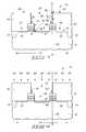
- a mask 50is formed over substrate 12 .
- Mask 50can comprise, for example, photoresist.
- Mask 50covers third portion 44 of active region 16 , but does not cover the second portion 42 of active region 16 . In other words, mask 50 does not cover the gap between transistor gate structures 20 and 22 .
- Mask 50has an opening 52 formed therein and extending over the gap between transistor gate structures 20 and 22 .
- Mask 50further comprises a top surface 54 , and an edge 56 of the top surface which defines an upper periphery of opening 52 .
- a vertical projection 58is shown extending upwardly through substrate 12 , and approximately perpendicular to upper surface 15 of the substrate.
- a second projection 60is defined to extend from top edge 56 to inner corner 29 .
- Second projection 60forms an angle “ ⁇ ” with vertical projection 58 .
- Angle “ ⁇ ”can be referred to as a threshold angle, as angle “ ⁇ ” defines a threshold dopant angle which determines if dopant can be implanted through opening 52 and to substrate 12 . Specifically, if dopant is implanted at an angle greater than “ ⁇ ”, the dopant will not reach substrate 12 . Instead, the dopant will impact sidewalls of opening 52 and portions of transistor gate structure 20 . Alternatively, if dopant is implanted at an angle less than the threshold angle, it will impact substrate 12 within the gap defined by region 42 .
- a first dopant 64is implanted into opening 52 at a first angle of approximately 0° relative to vertical projection 58 . Accordingly, dopant 64 is implanted at an angle less than the threshold angle “ ⁇ ”, and impacts substrate 12 within region 42 to form a implant region 66 .
- Dopant 64can comprise, for example, n type dopant (such as arsenic) and can be provided to a concentration of from about 10 18 atoms/cm 3 to about 10 19 atoms/cm 3 .
- a second dopant 70is implanted into opening 56 at an angle “ ⁇ ” relative to vertical projection 58 .
- Angle “ ⁇ ”is less than threshold angle “ ⁇ ” and accordingly dopant 70 impacts substrate 12 within region 42 to form a implant region 72 .
- implant region 72is shallower than region 66 . It is to be understood, however, that the invention encompasses other embodiments wherein region 72 is implanted to be deeper than region 66 .
- dopant 70comprises a p type dopant (such as boron), and is implanted at an angle “ ⁇ ” greater than about 0° and less than about 20°. Further, the p type dopant is implanted at an energy of at least about 25 KeV, and a dose of at least about 10 12 atoms/cm 2 .
- a third dopant 74is implanted at an angle “ ⁇ ” relative to vertical projection 58 , with angle “ ⁇ ” being greater than the threshold angle ⁇ . Accordingly, third dopant 74 does not reach substrate 12 .
- Third dopant 74can comprise, for example, p type dopant, and can be implanted at an angle “ ⁇ ” greater than or equal to 25°.
- the dopants 64 , 70 and 74can be implanted into a peripheral region (described with reference to FIG. 10) associated with substrate 12 simultaneously with the implant of the dopants into the shown DRAM region.
- Dopant 74can comprise an energy of at least about 50 KeV, and a dose of about 6 ⁇ 10 11 atoms/cm 2 .
- angle “ ⁇ ”is chosen to preclude impact of dopant 74 on substrate 12 within region 42 .
- dopant 74can be at an appropriate angle for implanting into regions of the substrate associated with various peripheral circuitry devices.
- a common maskcan be utilized during the entire doping sequence for implanting of dopants 64 , 70 and 74 .
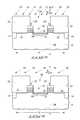
- a thin insulative layer 80is provided over exposed regions of substrate 12 , as well as along sidewalls of transistor gate structures 20 and 22 .
- Layer 80can comprise, for example, silicon dioxide formed by exposing substrate 12 and transistor gate structures 20 and 22 to oxidizing conditions. It is noted that the invention encompasses other embodiments (not shown) wherein layer 80 is not formed.
- a dopant 82is implanted into substrate 12 , after formation of layer 80 , to form an LDD implant 84 .
- LDD implant 84overlaps with the previous LDD implant 32 , and can comprise, for example, n-type dopant. It is to be understood that the invention encompasses embodiments wherein implant 82 is eliminated, as well as embodiments in which one of the implant regions 32 (FIG. 2) or 84 is eliminated, while the other is utilized. Accordingly, the implanting of dopants 64 , 70 and 74 can occur before formation of LDD regions, after formation of LDD regions, or between a first LDD implant and a second LDD implant.
- dopants 64 , 70 and 74can occur in any order relative to one another, such as, for example, with the implanting of the p-type dopants 70 and 74 occurring before the implanting of the n-type dopant 64 .
- sidewall spacers 90are formed along the sidewalls of transistor gate structures 20 and 22 .
- Sidewall spacers 90can comprise, for example, silicon dioxide or silicon nitride, and can be formed by anisotropically etching an appropriate insulative material layer.
- inner source/drain region location 42comprises a source/drain region 95
- outer source/drain region locations 44comprise source/drain regions 93 and 97 .
- Source/drain regions 93 and 95together with gate structure 20 , define a first transistor construction 99
- source/drain regions 95 and 97together with gate structure 22 , define a second transistor construction 101 .
- source/drain region 95is gatedly connected to source/drain regions 93 and 97 through transistor gates 20 and 22 , respectively.
- Source/drain region 95can be considered to be a shared source/drain region, in that it is shared by first transistor construction 99 and second transistor construction 101 .
- Shared source/drain region 95is different in dopant constituency than the outer source/drain regions 93 and 97 . Specifically, source/drain region 95 comprises halo regions 72 , and outer source/drain regions 93 and 97 do not comprise halo regions.
- NMOS transistor devicesi.e., devices in which the source/drain regions primarily comprise n-type regions, with a source/drain region which “primarily comprises n-type regions” being understood as a source/drain region which behaves generally as being n-type in character during operation of a device comprising the source/drain region
- the inventioncan also be utilized for formation of PMOS transistor devices. If the invention is utilized for formation of PMOS devices, the conductivity type of the regions 32 , 84 , 72 , 66 and 94 can be reversed relative to that described herein.
- conductivity regions 32 , 84 , 66 and 94are described as being n-type regions, but in a PMOS device such regions would correspond to p-type regions.
- region 72is described as being a p-type halo region in the shown NMOS construction, but in a PMOS construction would correspond to an n-type region.
- a DRAM construction 100is formed utilizing the transistor devices of FIG. 7. Specifically, an insulative material 110 is formed over substrate 12 , and conductive interconnects 112 , 114 and 116 extend through the insulative material 110 to the source/drain regions 93 , 95 , and 97 .
- Insulative material 110can comprise, for example, borophosphosilicate glass (BPSG), and conductive interconnects 112 can comprise, for example, one or more of conductively-doped silicon, metal silicide, and elemental metal.
- BPSGborophosphosilicate glass
- Conductive interconnect 114is electrically connected with a bitline 118 , which results in an electrical connection between shared source/drain region 95 and the bitline 118 .
- Electrical connections 112 and 116are incorporated into capacitor constructions 120 and 122 , respectively.
- a dielectric material 124is formed over electrical connections 112 and 116 , and a capacitor plate 126 is subsequently formed over the dielectric material 124 .
- conductive interconnects 112 and 116are incorporated into capacitor constructions 120 and 122 as storage nodes.
- Dielectric material 124can comprise, for example, one or more of silicon dioxide, silicon nitride, or so-called high K dielectric materials, such as tantalum pentoxide.
- Capacitor plates 126can comprise, for example, one or more of conductively-doped silicon, metal, or metal silicide.
- Transistor constructions 99 and 101define access transistors for the DRAM construction 100 , in than transistor constructions 99 and 101 are utilized to provide access between bitline 118 and the capacitor constructions 120 and 122 .
- FIGS. 7 and 8The processing described with reference to FIGS. 7 and 8 would typically occur while a mask is provided over peripheral circuitry, so that the processing of FIGS. 7 and 8 occurs only in a DRAM area of an integrated circuit structure. However, it should also be understood that various steps of the processing of FIGS. 7 and 8 will preferably be conducted simultaneously with steps utilized in the formation of peripheral circuit elements if a particular fabrication sequence is amenable to simultaneous formation of peripheral device components and DRAM memory components.
- the implants of FIGS. 4 and 5can provide particular advantages to DRAM structures formed in accordance with the present invention.
- the n-type implant 64(FIG. 4) reduces n-resistance of shared source/drain region 95 for improved drive current and improved hot electron reliability.
- the p-type angled implant 70(FIG. 5) increases the threshold voltage of the access devices 99 and 101 . Utilization of the p-type implant only relative to source/drain region 95 (and not relative to source/drain regions 93 and 97 ) allows the threshold voltage to be increased for the access transistors, while providing the halo implanting only on the digit side of the devices and thereby not disrupting careful control of graded junctions on the storage sides of the devices. It can be desired to maintain careful control of graded junction regions on the storage node side of an access transistor in order to minimize junction leakage and maintain adequate data retention for the DRAM memory.
- FIGS. 4 - 6can be utilized to simultaneously form implanted regions within logic circuitry peripheral to a DRAM memory array. If it is assumed that the wafer fragment 10 of FIGS. 4 - 6 is associated with a DRAM memory array region, than the wafer comprising fragment 10 can comprise another fragment associated with logic circuitry peripheral to the memory array region.
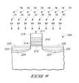
- FIG. 9illustrates a fragment 200 of the wafer. Fragment 200 is peripheral to the fragment 10 of FIGS. 1 - 8 , and is associated with logic circuitry.
- a transistor gate structure 211is shown formed over substrate 12 . Gate structure 211 comprises a gate oxide 212 , a silicon layer 214 , a silicide layer 216 and an insulative cap 218 .
- Layers 212 , 214 , 216 and 218can comprise the same materials as described previously for layer 24 , 26 , 28 and 30 , respectively.; Dopants 64 , 70 and 74 are shown being implanted into substrate 12 proximate structure 211 to form implant regions 220 , 222 and 224 , respectively.
- the implanting of dopants 64 , 70 and 74 into fragment 200preferably occurs simultaneously with the implanting of dopants 64 , 70 and 74 described previously with reference to FIGS. 4, 5 and 6 .
- the implanting of each of dopants 64 , 70 and 74is preferably blanket implanting in the sense that the dopants are simultaneously implanted over memory array regions and logic regions peripheral to the memory array regions.
Landscapes
- Physics & Mathematics (AREA)
- Engineering & Computer Science (AREA)
- High Energy & Nuclear Physics (AREA)
- Manufacturing & Machinery (AREA)
- Chemical & Material Sciences (AREA)
- Health & Medical Sciences (AREA)
- Toxicology (AREA)
- Crystallography & Structural Chemistry (AREA)
- Condensed Matter Physics & Semiconductors (AREA)
- General Physics & Mathematics (AREA)
- Computer Hardware Design (AREA)
- Microelectronics & Electronic Packaging (AREA)
- Power Engineering (AREA)
- Metal-Oxide And Bipolar Metal-Oxide Semiconductor Integrated Circuits (AREA)
- Semiconductor Memories (AREA)
Abstract
Description
- The invention pertains to DRAM devices, and to methods of forming DRAM devices. In particular aspects, the invention pertains to methods of forming access transistor constructions for DRAM devices.[0001]
- Dynamic random access memory (DRAM) is commonly utilized for computer memory. DRAM is incorporated into integrated circuit chips. Such chips frequently comprise a memory array of DRAM devices, and further comprise logic devices provided around a periphery of the memory array. The logic devices can be referred to as peripheral devices.[0002]
- There is a continuing goal to reduce the size of memory devices and peripheral devices to conserve valuable semiconductor substrate real estate. Another continuing goal is to utilize common fabrication steps during formation of peripheral and memory device structures to reduce the processing time utilized in forming a complete integrated circuit construction.[0003]
- It would be desirable to develop methods for DRAM fabrication which allow utilization of relatively small memory device structures, and it would be further desirable if such methods could utilize fabrication steps in common with the fabrication of peripheral device circuitry.[0004]
- In one aspect, the invention encompasses a method of forming a DRAM device. The device includes an access transistor construction having a pair of source/drain regions. A halo region is associated with one of the source/drain regions of the access transistor construction and no comparable halo region is associated with the other of the source/drain regions of the access transistor construction.[0005]
- In another aspect, the invention encompasses a method of forming a DRAM device. A substrate is provided, and the substrate has an active area defined therein. A pair of transistor gate structures are formed over the active area of the substrate. The transistor gate structures are spaced from one another by a gap, and the active area comprises a first portion covered by the transistor gate structures and a second portion between the transistor gate structures. The active area further comprises a third portion which is neither between the transistor gate structures or covered by the transistor gates structures. A mask is formed over the third portion of the active area while leaving the second portion uncovered. While the mask is over the third portion of the active area, dopant is implanted into the opening in the mask at an angle to reach through the gap and to the substrate. A pair of capacitor structures and a bitline are formed. The bitline is gatedly connected to one of the capacitor structures through one of the transistor gate structures, and gatedly connected to the other of the capacitor structures through the other of the transistor gate structures.[0006]
- In another aspect, the invention encompasses DRAM constructions.[0007]
- Preferred embodiments of the invention are described below with reference to the following accompanying drawings.[0008]
- FIG. 1 is a diagrammatic, cross-sectional view of a semiconductor wafer fragment shown at a preliminary processing step of a method of the present invention.[0009]
- FIG. 2 is a view of the FIG. 1 wafer fragment shown at a processing step subsequent to that of FIG. 1.[0010]
- FIG. 3 is a view of the FIG. 1 wafer fragment shown at a processing step subsequent to that of FIG. 2.[0011]
- FIG. 4 is a view of the FIG. 1 wafer fragment shown at a processing step subsequent to that of FIG. 3.[0012]
- FIG. 5 is a view of the FIG. 1 wafer fragment shown at a processing step subsequent to that of FIG. 4.[0013]
- FIG. 6 is a view of the FIG. 1 wafer fragment shown at a processing step subsequent to that of FIG. 5.[0014]
- FIG. 7 is a view of the FIG. 1 wafer fragment shown at a processing step subsequent to that of FIG. 6.[0015]
- FIG. 8 is a view of the FIG. 1 wafer fragment shown at a processing step subsequent to that of FIG. 7.[0016]
- FIG. 9 is a view of the wafer of FIG. 1, illustrating a different fragment that that of FIG. 1. Specifically, FIG. 9 illustrates a peripheral circuitry portion of the wafer of FIG. 1, and subjected to the processing of FIGS.[0017]4-6.
- A method of the present invention is described with reference to FIGS.[0018]1-10. Referring initially to FIG. 1, a
semiconductor wafer fragment 10 is illustrated at a preliminary processing step.Wafer fragment 10 comprises asubstrate 12 having anupper surface 15, andisolation regions 14 formed therein.Substrate 12 can comprise, for example, monocrystalline silicon lightly-doped with a background p-type dopant. To aid in interpretation of the claims that follow, the terms “semiconductive substrate” and “semiconductor substrate” are defined to mean any construction comprising semiconductive material, including, but not limited to, bulk semiconductive materials such as a semiconductive wafer (either alone or in assemblies comprising other materials thereon), and semiconductive material layers (either alone or in assemblies comprising other materials). The term “substrate” refers to any supporting structure, including, but not limited to, the semiconductive substrates described above. - [0019]
Isolation regions 14 can comprise, for example, shallow trench isolation regions comprising insulative material, such as silicon dioxide. Anactive region 16 is defined to extend betweenisolation regions 14.Active region 16 ultimately comprises source/drain regions (described with reference to FIGS.3-9) gatedly connected through transistor gate constructions (described with reference to FIG. 2). - Referring next to FIG. 2,[0020]
transistor gate constructions substrate 12.Transistor gate constructions Constructions dielectric layer 24, asilicon layer 26, ametal silicide layer 28, and aninsulative cap 30. Gatedielectric layer 24 will typically comprise silicon dioxide,silicon layer 26 will typically comprise conductively doped silicon,silicide layer 28 will typically comprise tungsten silicide or titanium silicide, andinsulative cap 30 will typically comprise silicon nitride or silicon dioxide. - It is to be understood that the shown layers of[0021]
gate constructions silicide layer 28 andinsulative cap 30. - [0022]
Gate constructions active area 16 into three regions. Specifically,gates constructions first region 40 ofactive area 16 as the region beneathconstructions second region 42 of theactive area 16 betweengate constructions third region 44, which is the remaining portion ofactive region 16 not encompassed by either the first or second regions. In the discussion that follows,regions 44 can be referred to as outer source/drain region locations, andregion 42 can be referred to as an inner source/drain region location. - [0023]
Transistor gate constructions region 42 ofactive area 16 between thegate structures Gate structure 20 comprises afirst sidewall 21 and asecond sidewall 23 in opposing relation tofirst sidewall 21; andstructure 22 comprises afirst sidewall 25 and asecond sidewall 27 in opposing relation tosidewall 25.Sidewalls sidewalls gate structures inner corners substrate 12. - Lightly doped diffusion regions (LDD regions)[0024]32 are shown formed within
substrate 12 andproximate structures regions 32 comprise n-type dopant provided to a concentration of less than or equal to 1018atoms/cm3withinsubstrate 12. It is noted that thediffusion regions 32 can be omitted in particular embodiments of the present invention. - Referring to FIG. 3, a[0025]
mask 50 is formed oversubstrate 12.Mask 50 can comprise, for example, photoresist.Mask 50 coversthird portion 44 ofactive region 16, but does not cover thesecond portion 42 ofactive region 16. In other words,mask 50 does not cover the gap betweentransistor gate structures Mask 50 has anopening 52 formed therein and extending over the gap betweentransistor gate structures Mask 50 further comprises atop surface 54, and anedge 56 of the top surface which defines an upper periphery ofopening 52. - A[0026]
vertical projection 58 is shown extending upwardly throughsubstrate 12, and approximately perpendicular toupper surface 15 of the substrate. Asecond projection 60 is defined to extend fromtop edge 56 toinner corner 29.Second projection 60 forms an angle “θ” withvertical projection 58. Angle “θ” can be referred to as a threshold angle, as angle “θ” defines a threshold dopant angle which determines if dopant can be implanted throughopening 52 and tosubstrate 12. Specifically, if dopant is implanted at an angle greater than “θ”, the dopant will not reachsubstrate 12. Instead, the dopant will impact sidewalls of opening52 and portions oftransistor gate structure 20. Alternatively, if dopant is implanted at an angle less than the threshold angle, it will impactsubstrate 12 within the gap defined byregion 42. - Referring to FIG. 4, a[0027]
first dopant 64 is implanted into opening52 at a first angle of approximately 0° relative tovertical projection 58. Accordingly,dopant 64 is implanted at an angle less than the threshold angle “θ”, and impactssubstrate 12 withinregion 42 to form aimplant region 66.Dopant 64 can comprise, for example, n type dopant (such as arsenic) and can be provided to a concentration of from about 1018atoms/cm3to about 1019atoms/cm3. - Referring next to FIG. 5, a[0028]
second dopant 70 is implanted into opening56 at an angle “α” relative tovertical projection 58. Angle “α” is less than threshold angle “θ” and accordingly dopant70impacts substrate 12 withinregion 42 to form aimplant region 72. In the shown embodiment,implant region 72 is shallower thanregion 66. It is to be understood, however, that the invention encompasses other embodiments whereinregion 72 is implanted to be deeper thanregion 66. In particular embodiments,dopant 70 comprises a p type dopant (such as boron), and is implanted at an angle “α” greater than about 0° and less than about 20°. Further, the p type dopant is implanted at an energy of at least about 25 KeV, and a dose of at least about 1012atoms/cm2. - Referring next to FIG. 5, a[0029]
third dopant 74 is implanted at an angle “β” relative tovertical projection 58, with angle “β” being greater than the threshold angle θ. Accordingly,third dopant 74 does not reachsubstrate 12.Third dopant 74 can comprise, for example, p type dopant, and can be implanted at an angle “β” greater than or equal to 25°. - The[0030]
dopants substrate 12 simultaneously with the implant of the dopants into the shown DRAM region.Dopant 74 can comprise an energy of at least about 50 KeV, and a dose of about 6×10¹¹atoms/cm2. In the shown embodiment, angle “β” is chosen to preclude impact ofdopant 74 onsubstrate 12 withinregion 42. However,dopant 74 can be at an appropriate angle for implanting into regions of the substrate associated with various peripheral circuitry devices. A common mask can be utilized during the entire doping sequence for implanting ofdopants - Referring to FIG. 7, mask[0031]50 (FIG. 6) is removed and a
thin insulative layer 80 is provided over exposed regions ofsubstrate 12, as well as along sidewalls oftransistor gate structures Layer 80 can comprise, for example, silicon dioxide formed by exposingsubstrate 12 andtransistor gate structures layer 80 is not formed. - A[0032]
dopant 82 is implanted intosubstrate 12, after formation oflayer 80, to form anLDD implant 84.LDD implant 84 overlaps with theprevious LDD implant 32, and can comprise, for example, n-type dopant. It is to be understood that the invention encompasses embodiments whereinimplant 82 is eliminated, as well as embodiments in which one of the implant regions32 (FIG. 2) or84 is eliminated, while the other is utilized. Accordingly, the implanting ofdopants dopants type dopants type dopant 64. - After formation of[0033]
layer 80,sidewall spacers 90 are formed along the sidewalls oftransistor gate structures Sidewall spacers 90 can comprise, for example, silicon dioxide or silicon nitride, and can be formed by anisotropically etching an appropriate insulative material layer. - In the processing step of FIG. 7, inner source/[0034]
drain region location 42 comprises a source/drain region 95, and outer source/drain region locations 44 comprise source/drain regions drain regions gate structure 20, define afirst transistor construction 99; and source/drain regions gate structure 22, define asecond transistor construction 101. In other words, source/drain region 95 is gatedly connected to source/drain regions transistor gates drain region 95 can be considered to be a shared source/drain region, in that it is shared byfirst transistor construction 99 andsecond transistor construction 101. - Shared source/[0035]
drain region 95 is different in dopant constituency than the outer source/drain regions drain region 95 compriseshalo regions 72, and outer source/drain regions - Although the shown invention comprises formation of NMOS transistor devices (i.e., devices in which the source/drain regions primarily comprise n-type regions, with a source/drain region which “primarily comprises n-type regions” being understood as a source/drain region which behaves generally as being n-type in character during operation of a device comprising the source/drain region), it is to be understood that the invention can also be utilized for formation of PMOS transistor devices. If the invention is utilized for formation of PMOS devices, the conductivity type of the[0036]
regions conductivity regions region 72 is described as being a p-type halo region in the shown NMOS construction, but in a PMOS construction would correspond to an n-type region. - Referring to FIG. 8, a[0037]
DRAM construction 100 is formed utilizing the transistor devices of FIG. 7. Specifically, aninsulative material 110 is formed oversubstrate 12, andconductive interconnects insulative material 110 to the source/drain regions Insulative material 110 can comprise, for example, borophosphosilicate glass (BPSG), andconductive interconnects 112 can comprise, for example, one or more of conductively-doped silicon, metal silicide, and elemental metal. - [0038]
Conductive interconnect 114 is electrically connected with abitline 118, which results in an electrical connection between shared source/drain region 95 and thebitline 118.Electrical connections capacitor constructions dielectric material 124 is formed overelectrical connections capacitor plate 126 is subsequently formed over thedielectric material 124. Accordingly,conductive interconnects capacitor constructions Dielectric material 124 can comprise, for example, one or more of silicon dioxide, silicon nitride, or so-called high K dielectric materials, such as tantalum pentoxide.Capacitor plates 126 can comprise, for example, one or more of conductively-doped silicon, metal, or metal silicide. - [0039]
Transistor constructions DRAM construction 100, in thantransistor constructions bitline 118 and thecapacitor constructions - The processing described with reference to FIGS. 7 and 8 would typically occur while a mask is provided over peripheral circuitry, so that the processing of FIGS. 7 and 8 occurs only in a DRAM area of an integrated circuit structure. However, it should also be understood that various steps of the processing of FIGS. 7 and 8 will preferably be conducted simultaneously with steps utilized in the formation of peripheral circuit elements if a particular fabrication sequence is amenable to simultaneous formation of peripheral device components and DRAM memory components.[0040]
- The implants of FIGS. 4 and 5 can provide particular advantages to DRAM structures formed in accordance with the present invention. The n-type implant[0041]64 (FIG. 4) reduces n-resistance of shared source/
drain region 95 for improved drive current and improved hot electron reliability. The p-type angled implant70 (FIG. 5) increases the threshold voltage of theaccess devices drain regions 93 and97) allows the threshold voltage to be increased for the access transistors, while providing the halo implanting only on the digit side of the devices and thereby not disrupting careful control of graded junctions on the storage sides of the devices. It can be desired to maintain careful control of graded junction regions on the storage node side of an access transistor in order to minimize junction leakage and maintain adequate data retention for the DRAM memory. - As described above, the processing of FIGS.[0042]4-6 can be utilized to simultaneously form implanted regions within logic circuitry peripheral to a DRAM memory array. If it is assumed that the
wafer fragment 10 of FIGS.4-6 is associated with a DRAM memory array region, than thewafer comprising fragment 10 can comprise another fragment associated with logic circuitry peripheral to the memory array region. FIG. 9 illustrates afragment 200 of the wafer.Fragment 200 is peripheral to thefragment 10 of FIGS.1-8, and is associated with logic circuitry. Atransistor gate structure 211 is shown formed oversubstrate 12.Gate structure 211 comprises agate oxide 212, asilicon layer 214, asilicide layer 216 and aninsulative cap 218.Layers layer Dopants substrate 12proximate structure 211 to formimplant regions dopants fragment 200 preferably occurs simultaneously with the implanting ofdopants dopants - In compliance with the statute, the invention has been described in language more or less specific as to structural and methodical features. It is to be understood, however, that the invention is not limited to the specific features shown and described, since the means herein disclosed comprise preferred forms of putting the invention into effect. The invention is, therefore, claimed in any of its forms or modifications within the proper scope of the appended claims appropriately interpreted in accordance with the doctrine of equivalents.[0043]
Claims (36)
Priority Applications (1)
| Application Number | Priority Date | Filing Date | Title |
|---|---|---|---|
| US10/325,159US7105881B2 (en) | 2001-08-07 | 2002-12-19 | DRAMS constructions and DRAM devices |
Applications Claiming Priority (3)
| Application Number | Priority Date | Filing Date | Title |
|---|---|---|---|
| US31093801P | 2001-08-07 | 2001-08-07 | |
| US09/941,375US6645806B2 (en) | 2001-08-07 | 2001-08-28 | Methods of forming DRAMS, methods of forming access transistors for DRAM devices, and methods of forming transistor source/drain regions |
| US10/325,159US7105881B2 (en) | 2001-08-07 | 2002-12-19 | DRAMS constructions and DRAM devices |
Related Parent Applications (1)
| Application Number | Title | Priority Date | Filing Date |
|---|---|---|---|
| US09/941,375DivisionUS6645806B2 (en) | 2001-08-07 | 2001-08-28 | Methods of forming DRAMS, methods of forming access transistors for DRAM devices, and methods of forming transistor source/drain regions |
Publications (2)
| Publication Number | Publication Date |
|---|---|
| US20030124788A1true US20030124788A1 (en) | 2003-07-03 |
| US7105881B2 US7105881B2 (en) | 2006-09-12 |
Family
ID=26977653
Family Applications (2)
| Application Number | Title | Priority Date | Filing Date |
|---|---|---|---|
| US09/941,375Expired - Fee RelatedUS6645806B2 (en) | 2001-08-07 | 2001-08-28 | Methods of forming DRAMS, methods of forming access transistors for DRAM devices, and methods of forming transistor source/drain regions |
| US10/325,159Expired - Fee RelatedUS7105881B2 (en) | 2001-08-07 | 2002-12-19 | DRAMS constructions and DRAM devices |
Family Applications Before (1)
| Application Number | Title | Priority Date | Filing Date |
|---|---|---|---|
| US09/941,375Expired - Fee RelatedUS6645806B2 (en) | 2001-08-07 | 2001-08-28 | Methods of forming DRAMS, methods of forming access transistors for DRAM devices, and methods of forming transistor source/drain regions |
Country Status (1)
| Country | Link |
|---|---|
| US (2) | US6645806B2 (en) |
Cited By (3)
| Publication number | Priority date | Publication date | Assignee | Title |
|---|---|---|---|---|
| US20050179074A1 (en)* | 2002-07-15 | 2005-08-18 | Koichi Kokubun | Semiconductor device and manufacturing method thereof |
| US20080119023A1 (en)* | 2006-11-16 | 2008-05-22 | Taiwan Semiconductor Manufacturing Company, Ltd. | Manufacturing method for semiconductor device to mitigate short channel effects |
| CN100444403C (en)* | 2004-04-13 | 2008-12-17 | 松下电器产业株式会社 | Semiconductor device and manufacturing method thereof |
Families Citing this family (10)
| Publication number | Priority date | Publication date | Assignee | Title |
|---|---|---|---|---|
| JP2003100902A (en)* | 2001-09-21 | 2003-04-04 | Mitsubishi Electric Corp | Method for manufacturing semiconductor device |
| KR100562650B1 (en)* | 2004-06-25 | 2006-03-20 | 주식회사 하이닉스반도체 | Semiconductor device manufacturing method |
| US20060046392A1 (en)* | 2004-08-26 | 2006-03-02 | Manning H M | Methods of forming vertical transistor structures |
| US7120046B1 (en) | 2005-05-13 | 2006-10-10 | Micron Technology, Inc. | Memory array with surrounding gate access transistors and capacitors with global and staggered local bit lines |
| US7371627B1 (en) | 2005-05-13 | 2008-05-13 | Micron Technology, Inc. | Memory array with ultra-thin etched pillar surround gate access transistors and buried data/bit lines |
| US7902598B2 (en)* | 2005-06-24 | 2011-03-08 | Micron Technology, Inc. | Two-sided surround access transistor for a 4.5F2 DRAM cell |
| US7888721B2 (en) | 2005-07-06 | 2011-02-15 | Micron Technology, Inc. | Surround gate access transistors with grown ultra-thin bodies |
| US7768051B2 (en) | 2005-07-25 | 2010-08-03 | Micron Technology, Inc. | DRAM including a vertical surround gate transistor |
| US7696567B2 (en) | 2005-08-31 | 2010-04-13 | Micron Technology, Inc | Semiconductor memory device |
| CN113380870B (en)* | 2020-02-25 | 2022-11-25 | 长鑫存储技术有限公司 | Semiconductor device fabrication method |
Citations (7)
| Publication number | Priority date | Publication date | Assignee | Title |
|---|---|---|---|---|
| US5134085A (en)* | 1991-11-21 | 1992-07-28 | Micron Technology, Inc. | Reduced-mask, split-polysilicon CMOS process, incorporating stacked-capacitor cells, for fabricating multi-megabit dynamic random access memories |
| US5439835A (en)* | 1993-11-12 | 1995-08-08 | Micron Semiconductor, Inc. | Process for DRAM incorporating a high-energy, oblique P-type implant for both field isolation and punchthrough |
| US6331725B1 (en)* | 1996-03-26 | 2001-12-18 | Micron Technology, Inc. | Integrated circuitry |
| US6380045B1 (en)* | 2000-03-24 | 2002-04-30 | Vanguard International Semiconductor Corp. | Method of forming asymmetric wells for DRAM cells |
| US6468876B2 (en)* | 1998-01-27 | 2002-10-22 | Texas Instruments Incorporated | Simple stack cell capacitor formation |
| US6545904B2 (en)* | 2001-03-16 | 2003-04-08 | Micron Technology, Inc. | 6f2 dram array, a dram array formed on a semiconductive substrate, a method of forming memory cells in a 6f2 dram array and a method of isolating a single row of memory cells in a 6f2 dram array |
| US6576965B2 (en)* | 1999-04-26 | 2003-06-10 | Mitsubishi Denki Kabushiki Kaisha | Semiconductor device with lightly doped drain layer |
Family Cites Families (4)
| Publication number | Priority date | Publication date | Assignee | Title |
|---|---|---|---|---|
| EP0575688B1 (en)* | 1992-06-26 | 1998-05-27 | STMicroelectronics S.r.l. | Programming of LDD-ROM cells |
| US5482878A (en)* | 1994-04-04 | 1996-01-09 | Motorola, Inc. | Method for fabricating insulated gate field effect transistor having subthreshold swing |
| US5661048A (en)* | 1995-03-21 | 1997-08-26 | Motorola, Inc. | Method of making an insulated gate semiconductor device |
| JP3061117B2 (en)* | 1997-06-18 | 2000-07-10 | 日本電気株式会社 | Method for manufacturing semiconductor device |
- 2001
- 2001-08-28USUS09/941,375patent/US6645806B2/ennot_activeExpired - Fee Related
- 2002
- 2002-12-19USUS10/325,159patent/US7105881B2/ennot_activeExpired - Fee Related
Patent Citations (7)
| Publication number | Priority date | Publication date | Assignee | Title |
|---|---|---|---|---|
| US5134085A (en)* | 1991-11-21 | 1992-07-28 | Micron Technology, Inc. | Reduced-mask, split-polysilicon CMOS process, incorporating stacked-capacitor cells, for fabricating multi-megabit dynamic random access memories |
| US5439835A (en)* | 1993-11-12 | 1995-08-08 | Micron Semiconductor, Inc. | Process for DRAM incorporating a high-energy, oblique P-type implant for both field isolation and punchthrough |
| US6331725B1 (en)* | 1996-03-26 | 2001-12-18 | Micron Technology, Inc. | Integrated circuitry |
| US6468876B2 (en)* | 1998-01-27 | 2002-10-22 | Texas Instruments Incorporated | Simple stack cell capacitor formation |
| US6576965B2 (en)* | 1999-04-26 | 2003-06-10 | Mitsubishi Denki Kabushiki Kaisha | Semiconductor device with lightly doped drain layer |
| US6380045B1 (en)* | 2000-03-24 | 2002-04-30 | Vanguard International Semiconductor Corp. | Method of forming asymmetric wells for DRAM cells |
| US6545904B2 (en)* | 2001-03-16 | 2003-04-08 | Micron Technology, Inc. | 6f2 dram array, a dram array formed on a semiconductive substrate, a method of forming memory cells in a 6f2 dram array and a method of isolating a single row of memory cells in a 6f2 dram array |
Cited By (5)
| Publication number | Priority date | Publication date | Assignee | Title |
|---|---|---|---|---|
| US20050179074A1 (en)* | 2002-07-15 | 2005-08-18 | Koichi Kokubun | Semiconductor device and manufacturing method thereof |
| US7417285B2 (en)* | 2002-07-15 | 2008-08-26 | Kabushiki Kaisha Toshiba | Semiconductor device having a trench capacitor and a MOSFET connected by a diffusion layer and manufacturing method thereof |
| CN100444403C (en)* | 2004-04-13 | 2008-12-17 | 松下电器产业株式会社 | Semiconductor device and manufacturing method thereof |
| US20080119023A1 (en)* | 2006-11-16 | 2008-05-22 | Taiwan Semiconductor Manufacturing Company, Ltd. | Manufacturing method for semiconductor device to mitigate short channel effects |
| US7449386B2 (en) | 2006-11-16 | 2008-11-11 | Taiwan Semiconductor Manufacturing Company, Ltd. | Manufacturing method for semiconductor device to mitigate short channel effects |
Also Published As
| Publication number | Publication date |
|---|---|
| US7105881B2 (en) | 2006-09-12 |
| US20030032229A1 (en) | 2003-02-13 |
| US6645806B2 (en) | 2003-11-11 |
Similar Documents
| Publication | Publication Date | Title |
|---|---|---|
| US5448090A (en) | Structure for reducing parasitic leakage in a memory array with merged isolation and node trench construction | |
| US6815281B1 (en) | Method of manufacturing a semiconductor device having a memory cell section and an adjacent circuit section | |
| US6417547B2 (en) | Semiconductor device with a halo structure | |
| US7518198B2 (en) | Transistor and method for manufacturing the same | |
| US6444548B2 (en) | Bitline diffusion with halo for improved array threshold voltage control | |
| US6399987B2 (en) | MOS transistor having self-aligned well bias area | |
| US6849890B2 (en) | Semiconductor device and manufacturing method thereof | |
| US6645806B2 (en) | Methods of forming DRAMS, methods of forming access transistors for DRAM devices, and methods of forming transistor source/drain regions | |
| US5981324A (en) | Methods of forming integrated circuits having memory cell arrays and peripheral circuits therein | |
| JPH0821694B2 (en) | Method for manufacturing ultra-high integrated semiconductor memory device | |
| US20030209758A1 (en) | Transistor of semiconductor device, and method for forming the same | |
| US4977099A (en) | Method for fabricating semiconductor memory device | |
| US5320976A (en) | Method for manufacturing VLSI semiconductor device | |
| US6274441B1 (en) | Method of forming bitline diffusion halo under gate conductor ledge | |
| US20010018243A1 (en) | Method for fabricating a semiconductor device | |
| US5926707A (en) | Methods for forming integrated circuit memory devices having deep storage electrode contact regions therein for improving refresh characteristics | |
| US6875666B2 (en) | Methods of manufacturing transistors and transistors having an anti-punchthrough region | |
| US6432787B1 (en) | Method and apparatus for providing low-GIDL dual workfunction gate doping with borderless diffusion contact | |
| US6750509B2 (en) | DRAM cell configuration and method for fabricating the DRAM cell configuration | |
| US6087213A (en) | Semiconductor memory device and manufacturing method thereof | |
| US6111283A (en) | Triple well structure | |
| US7186647B2 (en) | Method for fabricating semiconductor device having landing plug contact structure | |
| US20050199966A1 (en) | Dual work function semiconductor structure with borderless contact and method of fabricating the same | |
| US5593922A (en) | Method for buried contact isolation in SRAM devices | |
| US6967133B2 (en) | Method for fabricating a semiconductor structure |
Legal Events
| Date | Code | Title | Description |
|---|---|---|---|
| FEPP | Fee payment procedure | Free format text:PAYOR NUMBER ASSIGNED (ORIGINAL EVENT CODE: ASPN); ENTITY STATUS OF PATENT OWNER: LARGE ENTITY | |
| CC | Certificate of correction | ||
| AS | Assignment | Owner name:MOSAID TECHNOLOGIES INCORPORATED, CANADA Free format text:ASSIGNMENT OF ASSIGNORS INTEREST;ASSIGNOR:MICRON TECHNOLOGY, INC.;REEL/FRAME:023574/0723 Effective date:20090609 | |
| FPAY | Fee payment | Year of fee payment:4 | |
| AS | Assignment | Owner name:ROYAL BANK OF CANADA, CANADA Free format text:U.S. INTELLECTUAL PROPERTY SECURITY AGREEMENT (FOR NON-U.S. GRANTORS) - SHORT FORM;ASSIGNORS:658276 N.B. LTD.;658868 N.B. INC.;MOSAID TECHNOLOGIES INCORPORATED;REEL/FRAME:027512/0196 Effective date:20111223 | |
| FPAY | Fee payment | Year of fee payment:8 | |
| AS | Assignment | Owner name:CONVERSANT INTELLECTUAL PROPERTY MANAGEMENT INC., Free format text:CHANGE OF NAME;ASSIGNOR:MOSAID TECHNOLOGIES INCORPORATED;REEL/FRAME:032439/0638 Effective date:20140101 | |
| AS | Assignment | Owner name:CONVERSANT INTELLECTUAL PROPERTY MANAGEMENT INC., Free format text:RELEASE OF SECURITY INTEREST;ASSIGNOR:ROYAL BANK OF CANADA;REEL/FRAME:033484/0344 Effective date:20140611 Owner name:CONVERSANT IP N.B. 868 INC., CANADA Free format text:RELEASE OF SECURITY INTEREST;ASSIGNOR:ROYAL BANK OF CANADA;REEL/FRAME:033484/0344 Effective date:20140611 Owner name:CONVERSANT IP N.B. 276 INC., CANADA Free format text:RELEASE OF SECURITY INTEREST;ASSIGNOR:ROYAL BANK OF CANADA;REEL/FRAME:033484/0344 Effective date:20140611 | |
| AS | Assignment | Owner name:CONVERSANT INTELLECTUAL PROPERTY MANAGEMENT INC., CANADA Free format text:CHANGE OF ADDRESS;ASSIGNOR:CONVERSANT INTELLECTUAL PROPERTY MANAGEMENT INC.;REEL/FRAME:033678/0096 Effective date:20140820 Owner name:CONVERSANT INTELLECTUAL PROPERTY MANAGEMENT INC., Free format text:CHANGE OF ADDRESS;ASSIGNOR:CONVERSANT INTELLECTUAL PROPERTY MANAGEMENT INC.;REEL/FRAME:033678/0096 Effective date:20140820 | |
| AS | Assignment | Owner name:ROYAL BANK OF CANADA, AS LENDER, CANADA Free format text:U.S. PATENT SECURITY AGREEMENT (FOR NON-U.S. GRANTORS);ASSIGNOR:CONVERSANT INTELLECTUAL PROPERTY MANAGEMENT INC.;REEL/FRAME:033706/0367 Effective date:20140611 Owner name:CPPIB CREDIT INVESTMENTS INC., AS LENDER, CANADA Free format text:U.S. PATENT SECURITY AGREEMENT (FOR NON-U.S. GRANTORS);ASSIGNOR:CONVERSANT INTELLECTUAL PROPERTY MANAGEMENT INC.;REEL/FRAME:033706/0367 Effective date:20140611 | |
| FEPP | Fee payment procedure | Free format text:MAINTENANCE FEE REMINDER MAILED (ORIGINAL EVENT CODE: REM.) | |
| AS | Assignment | Owner name:CONVERSANT INTELLECTUAL PROPERTY MANAGEMENT INC., CANADA Free format text:RELEASE OF U.S. PATENT AGREEMENT (FOR NON-U.S. GRANTORS);ASSIGNOR:ROYAL BANK OF CANADA, AS LENDER;REEL/FRAME:047645/0424 Effective date:20180731 Owner name:CONVERSANT INTELLECTUAL PROPERTY MANAGEMENT INC., Free format text:RELEASE OF U.S. PATENT AGREEMENT (FOR NON-U.S. GRANTORS);ASSIGNOR:ROYAL BANK OF CANADA, AS LENDER;REEL/FRAME:047645/0424 Effective date:20180731 | |
| LAPS | Lapse for failure to pay maintenance fees | Free format text:PATENT EXPIRED FOR FAILURE TO PAY MAINTENANCE FEES (ORIGINAL EVENT CODE: EXP.); ENTITY STATUS OF PATENT OWNER: LARGE ENTITY | |
| STCH | Information on status: patent discontinuation | Free format text:PATENT EXPIRED DUE TO NONPAYMENT OF MAINTENANCE FEES UNDER 37 CFR 1.362 | |
| FP | Lapsed due to failure to pay maintenance fee | Effective date:20180912 |