US20030124465A1 - Method for fabricating semiconductor device capable of covering facet on plug - Google Patents
Method for fabricating semiconductor device capable of covering facet on plugDownload PDFInfo
- Publication number
- US20030124465A1 US20030124465A1US10/293,497US29349702AUS2003124465A1US 20030124465 A1US20030124465 A1US 20030124465A1US 29349702 AUS29349702 AUS 29349702AUS 2003124465 A1US2003124465 A1US 2003124465A1
- Authority
- US
- United States
- Prior art keywords
- insulation layer
- layer
- plug
- planarization
- recited
- Prior art date
- Legal status (The legal status is an assumption and is not a legal conclusion. Google has not performed a legal analysis and makes no representation as to the accuracy of the status listed.)
- Abandoned
Links
- 238000000034methodMethods0.000titleclaimsabstractdescription58
- 239000004065semiconductorSubstances0.000titleclaimsabstractdescription13
- 238000009413insulationMethods0.000claimsabstractdescription60
- 230000008569processEffects0.000claimsabstractdescription37
- 230000001681protective effectEffects0.000claimsabstractdescription15
- 230000007547defectEffects0.000claimsabstractdescription12
- 238000004140cleaningMethods0.000claimsabstractdescription9
- 239000000758substrateSubstances0.000claimsabstractdescription7
- 230000009969flowable effectEffects0.000claimsdescription11
- BOTDANWDWHJENH-UHFFFAOYSA-NTetraethyl orthosilicateChemical compoundCCO[Si](OCC)(OCC)OCCBOTDANWDWHJENH-UHFFFAOYSA-N0.000claimsdescription9
- BLRPTPMANUNPDV-UHFFFAOYSA-NSilaneChemical compound[SiH4]BLRPTPMANUNPDV-UHFFFAOYSA-N0.000claimsdescription5
- 239000005368silicate glassSubstances0.000claimsdescription3
- 238000010790dilutionMethods0.000claimsdescription2
- 239000012895dilutionSubstances0.000claimsdescription2
- XLYOFNOQVPJJNP-UHFFFAOYSA-NwaterSubstancesOXLYOFNOQVPJJNP-UHFFFAOYSA-N0.000claimsdescription2
- 230000000694effectsEffects0.000abstract1
- 239000010410layerSubstances0.000description89
- 238000000151depositionMethods0.000description7
- 239000011229interlayerSubstances0.000description7
- 238000005530etchingMethods0.000description6
- 230000008901benefitEffects0.000description3
- 230000007423decreaseEffects0.000description3
- 229920002120photoresistant polymerPolymers0.000description3
- 125000006850spacer groupChemical group0.000description3
- 239000000126substanceSubstances0.000description3
- 229910052581Si3N4Inorganic materials0.000description2
- 230000015572biosynthetic processEffects0.000description2
- 230000008021depositionEffects0.000description2
- 238000005755formation reactionMethods0.000description2
- 238000004518low pressure chemical vapour depositionMethods0.000description2
- 238000005498polishingMethods0.000description2
- 229910021420polycrystalline siliconInorganic materials0.000description2
- 229920005591polysiliconPolymers0.000description2
- HQVNEWCFYHHQES-UHFFFAOYSA-Nsilicon nitrideChemical compoundN12[Si]34N5[Si]62N3[Si]51N64HQVNEWCFYHHQES-UHFFFAOYSA-N0.000description2
- 229910052814silicon oxideInorganic materials0.000description2
- -1silicon oxide nitrideChemical class0.000description2
- WFKWXMTUELFFGS-UHFFFAOYSA-NtungstenChemical compound[W]WFKWXMTUELFFGS-UHFFFAOYSA-N0.000description2
- 239000010937tungstenSubstances0.000description2
- 229910052721tungstenInorganic materials0.000description2
- 239000011800void materialSubstances0.000description2
- ATJFFYVFTNAWJD-UHFFFAOYSA-NTinChemical compound[Sn]ATJFFYVFTNAWJD-UHFFFAOYSA-N0.000description1
- 230000004888barrier functionEffects0.000description1
- 230000015556catabolic processEffects0.000description1
- 239000007806chemical reaction intermediateSubstances0.000description1
- 238000005229chemical vapour depositionMethods0.000description1
- 239000011248coating agentSubstances0.000description1
- 238000000576coating methodMethods0.000description1
- 230000000295complement effectEffects0.000description1
- 239000004020conductorSubstances0.000description1
- 238000006731degradation reactionMethods0.000description1
- 238000009792diffusion processMethods0.000description1
- 230000003292diminished effectEffects0.000description1
- 239000012535impuritySubstances0.000description1
- 229910052751metalInorganic materials0.000description1
- 239000002184metalSubstances0.000description1
- 239000000203mixtureSubstances0.000description1
- 230000004048modificationEffects0.000description1
- 238000012986modificationMethods0.000description1
- 150000004767nitridesChemical class0.000description1
- 239000011241protective layerSubstances0.000description1
- 239000000376reactantSubstances0.000description1
- 229910021332silicideInorganic materials0.000description1
- FVBUAEGBCNSCDD-UHFFFAOYSA-Nsilicide(4-)Chemical compound[Si-4]FVBUAEGBCNSCDD-UHFFFAOYSA-N0.000description1
- 239000002356single layerSubstances0.000description1
- WQJQOUPTWCFRMM-UHFFFAOYSA-Ntungsten disilicideChemical compound[Si]#[W]#[Si]WQJQOUPTWCFRMM-UHFFFAOYSA-N0.000description1
- 229910021342tungsten silicideInorganic materials0.000description1
Images


Classifications
- H—ELECTRICITY
- H01—ELECTRIC ELEMENTS
- H01L—SEMICONDUCTOR DEVICES NOT COVERED BY CLASS H10
- H01L21/00—Processes or apparatus adapted for the manufacture or treatment of semiconductor or solid state devices or of parts thereof
- H01L21/02—Manufacture or treatment of semiconductor devices or of parts thereof
- H01L21/04—Manufacture or treatment of semiconductor devices or of parts thereof the devices having potential barriers, e.g. a PN junction, depletion layer or carrier concentration layer
- H01L21/18—Manufacture or treatment of semiconductor devices or of parts thereof the devices having potential barriers, e.g. a PN junction, depletion layer or carrier concentration layer the devices having semiconductor bodies comprising elements of Group IV of the Periodic Table or AIIIBV compounds with or without impurities, e.g. doping materials
- H01L21/28—Manufacture of electrodes on semiconductor bodies using processes or apparatus not provided for in groups H01L21/20 - H01L21/268
- H—ELECTRICITY
- H01—ELECTRIC ELEMENTS
- H01L—SEMICONDUCTOR DEVICES NOT COVERED BY CLASS H10
- H01L21/00—Processes or apparatus adapted for the manufacture or treatment of semiconductor or solid state devices or of parts thereof
- H01L21/70—Manufacture or treatment of devices consisting of a plurality of solid state components formed in or on a common substrate or of parts thereof; Manufacture of integrated circuit devices or of parts thereof
- H01L21/71—Manufacture of specific parts of devices defined in group H01L21/70
- H01L21/768—Applying interconnections to be used for carrying current between separate components within a device comprising conductors and dielectrics
- H01L21/76897—Formation of self-aligned vias or contact plugs, i.e. involving a lithographically uncritical step
- H—ELECTRICITY
- H01—ELECTRIC ELEMENTS
- H01L—SEMICONDUCTOR DEVICES NOT COVERED BY CLASS H10
- H01L21/00—Processes or apparatus adapted for the manufacture or treatment of semiconductor or solid state devices or of parts thereof
- H01L21/70—Manufacture or treatment of devices consisting of a plurality of solid state components formed in or on a common substrate or of parts thereof; Manufacture of integrated circuit devices or of parts thereof
- H01L21/71—Manufacture of specific parts of devices defined in group H01L21/70
- H01L21/768—Applying interconnections to be used for carrying current between separate components within a device comprising conductors and dielectrics
- H01L21/76838—Applying interconnections to be used for carrying current between separate components within a device comprising conductors and dielectrics characterised by the formation and the after-treatment of the conductors
- H01L21/76877—Filling of holes, grooves or trenches, e.g. vias, with conductive material
Definitions
- the present inventionrelates to a method for fabricating a semiconductor device; and, more particularly, to a method for covering a facet on plug.
- the plugis formed after performing an etch process, which is one of processes for fabricating a semiconductor device.
- the SEG for forming the plughas an advantage in reducing a contact resistance 1.5 times greater than using a typical deposition technique.
- a high density plasma (hereinafter referred as to HDP) oxide layeris deposited as an inter-layer insulation layer and a chemical mechanical polishing (hereinafter referred as to CMP) is performed to isolate the plug.
- the HDP oxide layeris an oxide layer deposited in an apparatus providing high density plasma. After the CMP, the following two cases are proceeded.
- an undoped silicate glasshereinafter referred as to USG
- USGundoped silicate glass
- a bit lineis formed after forming a bit line contact hole by an etching the USG.
- a HDP oxide layeris formed, an etch back process using a plasma is performed, and a bit line is formed after forming a bit line contact hole by etching the HDP oxide layer.
- a micro-dishing phenomenonoccurs by applying the CMP process to the HDP oxide layer, which results in a short between the bit lines.
- defectsuch as a micro void or an opening
- these defectsprogress substantially further through the step of applying an etch back to the HDP oxide layer.
- subsequent etch processes for forming a bit line contact hole or a bit line with tungsten Wmore defects are generated due to a micro-step difference resulted from the above defect and the void.
- DOFdepth of focus
- APLadvanced planarization layer
- CVDself planarization chemical vapor deposition
- the self planarization CVDuses a low pressure chemical vapor deposition (hereinafter referred as to LPCVD) to ultimately form the planarized inter-layer insulation layer with use of H 2 O 2 and SiH 4 as a reactant source and has an excellent gap-fill property due to its flow property.
- LPCVDlow pressure chemical vapor deposition
- the flowable inter-layer insulation layerpossesses an excellent gap-fill property, high stability of a layer, no occurrence of cracks and lifting, low thermal budget because of the deposition performed at a temperature less than 650° C., tolerance to a temperature greater than 1000° C. and tolerance to strong chemicals and a property of planarization.
- the flowable interlayer insulation layerhas a high rate of an etching speed when performing a pre-cleaning process in accordance with a wet cleaning that employs an etchant such as HF or a buffered oxide etchant (hereinafter referred as to BOE).
- an etchantsuch as HF or a buffered oxide etchant (hereinafter referred as to BOE).
- the dilution of the etchant to the wateris from about 100:1 to about 500:1. Therefore, top critical dimension widening phenomenon is observed and this phenomenon results in a decrease of the overlap margin between a bit line and a bit line contact during a process for forming the bit line after depositing a conductive material.
- an object of the present inventionto provide a method for fabricating a semiconductor device capable of improving an overlap margin during a formation of a conductive layer, such as a bit line or a bit line contact.
- a method for fabricating a semiconductor devicecomprising the steps of: forming a plug passing through an insulation layer to be contacted with a substrate board; forming a planarization insulation layer on an entire surface including the plug so as to cover defects appeared at a surface of the plug; forming a protective insulation layer on the planarization insulation layer for preventing losses of the planarization insulation layer resulted from a subsequent cleaning process; performing a process with an etchant; and forming a conductive layer contacted to the plug by passing through the protective insulation layer and the planarization insulation layer.
- a flowable insulation layer or an undoped silicate glass (USG) layer that formed with SiH 4 , that is a facet on the top portion of the plug, which results in subsequent defects occurring at a later processes for forming a bit line and a bit line contactis covered with a flowable insulation layer or the USG layer.
- a tetra ethyl ortho silicate (TEOS) layer or a high density plasma (HDP) oxide layeris stacked on the flowable insulation layer or the USG layer.
- FIGS. 1 to 5are cross-sectional views illustrating a fabricating process of a semiconductor device in accordance with a preferred embodiment of the present invention.
- a number of conductive patternsare formed on a substrate 10 .
- the conductive patternsare bit lines or gate electrodes, and the gate electrodes will be taken as an exemplary conductive pattern for this preferred embodiment.
- oxide layer based gate insulation layer 11a conductive layer 12 for gate electrode and a nitride layer for a hard mask 13 are sequentially deposited and a photo-etch process is performed with a mask to form a gate electrode.
- the conductive layer 12 for the gate electrodeis formed with a single or mixtures of polysilicon layer, tungsten layer and tungsten silicide layer.
- a spacer 14is formed to protect lateral sides of the gate insulation layer 11 and the conductive layer 12 .
- the spacer 14is formed by depositing and etching a silicon nitride layer or silicon oxide nitride layer.
- the silicon nitride layer or the silicon oxide nitride layeris deposited to a thickness ranging from about 100 ⁇ to about 500 ⁇ .
- An inter-layer insulation layer 15is deposited as much as possible to fill spaces between neighboring patterns, i.e., the spacers 14 .
- a surface of the substrate 10 between the gate electrodese.g., a source or a drain, a impurity diffusion area, is opened through an etch process.
- a plug 16 contacted to the surface of the substrate 10is formed by a selective epitaxial growth (hereinafter referred as to SEG) or a deposition of a polysilicon layer.
- SEGselective epitaxial growth
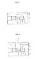
- a facet 17is generated as shown in FIG. 1.
- HDPhigh density plasma
- a planarization processsuch as chemical mechanical polishing (hereinafter referred as to CMP) process or dry etch back process is applied to the insulation layer 18 so as to isolate each plug 16 formed.
- CMPchemical mechanical polishing
- dry etch back processis applied to the insulation layer 18 so as to isolate each plug 16 formed.
- the facet 17is still remained and becomes a burden when forming a conductive pattern, such as a bit line or a bit line contact.
- the planarization insulation layer 19is formed with a flowable insulation layer or USG layer using siH 4 .
- a protective insulation layer 20is formed with a tetra ethyl ortho silicate (hereinafter referred as to TEOS) layer or a HDP oxide layer for preventing losses of the planarization insulation layer 19 in a subsequent cleaning process. It is possible for the protective insulation layer 20 to protect the planarization insulation layer 19 during the actual operation of the cleaning process.
- a thickness of the protective insulation layer 20is in a range from about 500 ⁇ to about 3000 ⁇ .
- a thickness of the protective insulation layer 20is in a range from about 500 ⁇ to about 3000 ⁇ , whereas the thickness is in a range from about 500 ⁇ to about 3000 ⁇ in case of using SiH 4 .
- a process with an etchantsuch as an etching or a cleaning, is carried out.
- an etchantsuch as an etching or a cleaning.
- an etch processis described as follows.
- a photoresist pattern 21 for forming a contact holeis formed on the protective insulation layer 20 .
- the photoresist pattern 21functions as an etch mask when the planarization insulation layer 19 and the protective insulation layer 20 are sequentially etched with HF or buffered oxide etchant(herein after referred as BOE). Because of this etching process, an opening portion 22 that exposes a surface of the plug 16 is formed. Concurrently, since the planarization insulation layer 19 and the protective layer 20 complement defects occurred at bottom portions of the semiconductor device while simultaneously achieving the layer planarization, it is possible to attain a process margin at the steps of coating and exposing a photoresist.
- the opening portion 22is filled with a conductive layer 23 contacted to the plug 16 .
- the conductive layer 23is formed with a single layer or multi-layers of W, WSi or metal silicide in till reaching a thickness in a range from about 500 ⁇ to about 3000 ⁇ .
- a barrier layer(not shown)can be formed additionally on an interface between the conductive layer 23 and the plug 16 with a thickness in a range from about 50 ⁇ to about 1000 ⁇ by using Ti, TiN, TiW, TaW, TaN or WN and so on. It is possible to prevent short between conductive patterns such as bit line, due to the planarization of the insulation layer in accordance with the preferred embodiment of the present invention.
- the preferred embodimentclearly demonstrates that it is possible to overcome defects such as the facet on the plug surface and problems resulted from the cleaning process through the formations of the planarization insulation layer, e.g., flowable insulation layer and the protective insulation layer, e.g., TEOS layer on the top surface of the plug.
- the planarization insulation layere.g., flowable insulation layer
- the protective insulation layere.g., TEOS layer
Landscapes
- Engineering & Computer Science (AREA)
- Physics & Mathematics (AREA)
- Condensed Matter Physics & Semiconductors (AREA)
- General Physics & Mathematics (AREA)
- Manufacturing & Machinery (AREA)
- Computer Hardware Design (AREA)
- Microelectronics & Electronic Packaging (AREA)
- Power Engineering (AREA)
- Internal Circuitry In Semiconductor Integrated Circuit Devices (AREA)
Abstract
Description
- The present invention relates to a method for fabricating a semiconductor device; and, more particularly, to a method for covering a facet on plug.[0001]
- There has been actively studied on a method for forming a plug by performing a selective epitaxial growth (hereinafter referred as to SEG). The plug is formed after performing an etch process, which is one of processes for fabricating a semiconductor device. The SEG for forming the plug has an advantage in reducing a contact resistance 1.5 times greater than using a typical deposition technique. On the other hand, after performing the SEG, a high density plasma (hereinafter referred as to HDP) oxide layer is deposited as an inter-layer insulation layer and a chemical mechanical polishing (hereinafter referred as to CMP) is performed to isolate the plug. The HDP oxide layer is an oxide layer deposited in an apparatus providing high density plasma. After the CMP, the following two cases are proceeded. For one case, an undoped silicate glass (hereinafter referred as to USG) is deposited, and a bit line is formed after forming a bit line contact hole by an etching the USG. For another case, a HDP oxide layer is formed, an etch back process using a plasma is performed, and a bit line is formed after forming a bit line contact hole by etching the HDP oxide layer.[0002]
- However, there result in problems when proceeding the above mentioned processes. A micro-dishing phenomenon occurs by applying the CMP process to the HDP oxide layer, which results in a short between the bit lines. When a SEG facet is excessively developed, defect, such as a micro void or an opening, is generated in a HDP oxide layer at the step of depositing the HPD oxide layer. Especially, these defects progress substantially further through the step of applying an etch back to the HDP oxide layer. During subsequent etch processes for forming a bit line contact hole or a bit line with tungsten W, more defects are generated due to a micro-step difference resulted from the above defect and the void. Thus, a shortage of a depth of focus (DOF) margin during a photo-etch process is induced, and a device failure is generated.[0003]
- Meanwhile, in case of a next generation semiconductor device, an overlap margin between the bit line and the bit line contact hole decreases remarkably because of diminished restrictions in layout and process aspects.[0004]
- In a method for fabricating a semiconductor device having a line width less than 0.1 μm, spaces of the contact hole and so forth decrease while an aspect ratio increases. Thus, it is impossible to carry out a complete filling, with respect to a gap-fill property of an insulating, thereby resulting in problems of voids. In order to solve these problems, a technology to form a flowable insulation layer has been actively studied. An advanced planarization layer (APL) thin layer is an insulation layer having a flow property.[0005]
- Among various techniques related to the APL thin layer, self planarization chemical vapor deposition (hereinafter referred as to CVD) forms a reaction intermediate having a substantially high degree of fluidity, and thus, a complete filling planarization can be attained when forming a layer. Hence, a planarized inter-layer insulation layer can be formed through a simple single process, which, in turn, allows process costs to be reduced effectively compared to use of a typical complex process. In more detail, the self planarization CVD uses a low pressure chemical vapor deposition (hereinafter referred as to LPCVD) to ultimately form the planarized inter-layer insulation layer with use of H[0006]2O2and SiH4as a reactant source and has an excellent gap-fill property due to its flow property.
- In summary, the flowable inter-layer insulation layer possesses an excellent gap-fill property, high stability of a layer, no occurrence of cracks and lifting, low thermal budget because of the deposition performed at a temperature less than 650° C., tolerance to a temperature greater than 1000° C. and tolerance to strong chemicals and a property of planarization.[0007]
- In spite of all these advantages, the flowable interlayer insulation layer has a high rate of an etching speed when performing a pre-cleaning process in accordance with a wet cleaning that employs an etchant such as HF or a buffered oxide etchant (hereinafter referred as to BOE). The dilution of the etchant to the water is from about 100:1 to about 500:1. Therefore, top critical dimension widening phenomenon is observed and this phenomenon results in a decrease of the overlap margin between a bit line and a bit line contact during a process for forming the bit line after depositing a conductive material.[0008]
- It is, therefore, an object of the present invention to provide a method for fabricating a semiconductor device capable of improving an overlap margin during a formation of a conductive layer, such as a bit line or a bit line contact.[0009]
- In accordance with an aspect of the present invention, there is provided a method for fabricating a semiconductor device, comprising the steps of: forming a plug passing through an insulation layer to be contacted with a substrate board; forming a planarization insulation layer on an entire surface including the plug so as to cover defects appeared at a surface of the plug; forming a protective insulation layer on the planarization insulation layer for preventing losses of the planarization insulation layer resulted from a subsequent cleaning process; performing a process with an etchant; and forming a conductive layer contacted to the plug by passing through the protective insulation layer and the planarization insulation layer.[0010]
- In accordance with the present invention, during a planarization process for forming a plug, surface defects are covered with a flowable insulation layer or an undoped silicate glass (USG) layer that formed with SiH[0011]4, that is a facet on the top portion of the plug, which results in subsequent defects occurring at a later processes for forming a bit line and a bit line contact, is covered with a flowable insulation layer or the USG layer. A tetra ethyl ortho silicate (TEOS) layer or a high density plasma (HDP) oxide layer is stacked on the flowable insulation layer or the USG layer.
- The above and other objects and features of the present invention will become apparent from the following description of the preferred embodiments given in conjunction with the accompanying drawings, in which:[0012]
- FIGS.[0013]1 to5 are cross-sectional views illustrating a fabricating process of a semiconductor device in accordance with a preferred embodiment of the present invention.
- First of all, with reference to FIG. 1, a number of conductive patterns are formed on a[0014]
substrate 10. The conductive patterns are bit lines or gate electrodes, and the gate electrodes will be taken as an exemplary conductive pattern for this preferred embodiment. - In more detail, oxide layer based[0015]
gate insulation layer 11, aconductive layer 12 for gate electrode and a nitride layer for ahard mask 13 are sequentially deposited and a photo-etch process is performed with a mask to form a gate electrode. In this preferred embodiment, theconductive layer 12 for the gate electrode is formed with a single or mixtures of polysilicon layer, tungsten layer and tungsten silicide layer. - Then, a[0016]
spacer 14 is formed to protect lateral sides of thegate insulation layer 11 and theconductive layer 12. At this time, thespacer 14 is formed by depositing and etching a silicon nitride layer or silicon oxide nitride layer. In this preferred embodiment, the silicon nitride layer or the silicon oxide nitride layer is deposited to a thickness ranging from about 100 Å to about 500 Å. - An[0017]
inter-layer insulation layer 15 is deposited as much as possible to fill spaces between neighboring patterns, i.e., thespacers 14. After depositing theinter-layer insulation layer 15, a surface of thesubstrate 10 between the gate electrodes, e.g., a source or a drain, a impurity diffusion area, is opened through an etch process. Then, aplug 16 contacted to the surface of thesubstrate 10 is formed by a selective epitaxial growth (hereinafter referred as to SEG) or a deposition of a polysilicon layer. At this time, afacet 17 is generated as shown in FIG. 1. - Next, an insulation layer(not shown) is formed to isolate the neighboring[0018]
plug 16 with use of a high density plasma (hereinafter referred as to HDP) oxide layer. - Referring to FIG. 2, a planarization process such as chemical mechanical polishing (hereinafter referred as to CMP) process or dry etch back process is applied to the insulation layer[0019]18 so as to isolate each
plug 16 formed. Despite of this planarization process, thefacet 17 is still remained and becomes a burden when forming a conductive pattern, such as a bit line or a bit line contact. - Accordingly, as shown in FIG. 3, a[0020]
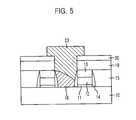
planarization insulation layer 19 for covering a surface defect, i.e., thefacet 17, is formed on an entire surface of thesubstrate 10 including theplug 16. In this preferred embodiment, theplanarization insulation layer 19 is formed with a flowable insulation layer or USG layer using siH4. - On the[0021]
planarization layer 19, aprotective insulation layer 20 is formed with a tetra ethyl ortho silicate (hereinafter referred as to TEOS) layer or a HDP oxide layer for preventing losses of theplanarization insulation layer 19 in a subsequent cleaning process. It is possible for theprotective insulation layer 20 to protect theplanarization insulation layer 19 during the actual operation of the cleaning process. In case of using the HDP oxide layer, a thickness of theprotective insulation layer 20 is in a range from about 500 Å to about 3000 Å. On the other hand, in case of using the TEOS layer, a thickness of theprotective insulation layer 20 is in a range from about 500 Å to about 3000 Å, whereas the thickness is in a range from about 500 Å to about 3000 Å in case of using SiH4. - After forming the[0022]
protective insulation layer 20, a process with an etchant, such as an etching or a cleaning, is carried out. In the preferred embodiment, an etch process is described as follows. - Referring to FIG. 4, a[0023]
photoresist pattern 21 for forming a contact hole is formed on theprotective insulation layer 20. Thephotoresist pattern 21 functions as an etch mask when theplanarization insulation layer 19 and theprotective insulation layer 20 are sequentially etched with HF or buffered oxide etchant(herein after referred as BOE). Because of this etching process, anopening portion 22 that exposes a surface of theplug 16 is formed. Concurrently, since theplanarization insulation layer 19 and theprotective layer 20 complement defects occurred at bottom portions of the semiconductor device while simultaneously achieving the layer planarization, it is possible to attain a process margin at the steps of coating and exposing a photoresist. - With reference to FIG. 5, the[0024]
opening portion 22 is filled with aconductive layer 23 contacted to theplug 16. Theconductive layer 23 is formed with a single layer or multi-layers of W, WSi or metal silicide in till reaching a thickness in a range from about 500 Å to about 3000 Å. Also, a barrier layer(not shown) can be formed additionally on an interface between theconductive layer 23 and theplug 16 with a thickness in a range from about 50 Å to about 1000 Å by using Ti, TiN, TiW, TaW, TaN or WN and so on. It is possible to prevent short between conductive patterns such as bit line, due to the planarization of the insulation layer in accordance with the preferred embodiment of the present invention. - As described above, the preferred embodiment clearly demonstrates that it is possible to overcome defects such as the facet on the plug surface and problems resulted from the cleaning process through the formations of the planarization insulation layer, e.g., flowable insulation layer and the protective insulation layer, e.g., TEOS layer on the top surface of the plug. As a result of these advantages, a process margin can also be improved during a subsequent process and degradation of semiconductor device properties can be ultimately prevented.[0025]
- While the present invention has been described with respect to certain preferred embodiments, it will be apparent to those skilled in the art that various changes and modifications may be made without departing from the scope of the invention as defined in the following claims.[0026]
Claims (11)
1. A method for fabricating a semiconductor device, comprising the steps of:
forming a plug passing through an insulation layer to be contacted with a substrate;
forming a planarization insulation layer on an entire surface including the plug so as to cover defects appeared at a surface of the plug;
forming a protective insulation layer on the planarization insulation layer for preventing losses of the planarization insulation layer resulted from a subsequent cleaning process;
performing a process with an etchant; and
forming a conductive layer contacted to the plug by passing through the protective insulation layer and the planarization insulation layer.
2. The method as recited inclaim 1 , wherein the etchant is dilute HF or BOE.
3. The method as recited inclaim 2 , wherein the dilution of the etchant to the water is from about 100:1 to about 500:1.
4. The method as recited inclaim 1 , wherein the planarization insulation layer includes a flowable insulation layer or a undoped silicate glass (USG) layer that uses SiH4.
5. The method as recited inclaim 4 , wherein the flowable insulation layer is An advanced planarization layer.
6. The method as recited inclaim 4 , wherein the flowable insulation layer is formed with a thickness in a range from about 500 Å to about 3000 Å.
7. The method as recited inclaim 4 , wherein the USG layer that uses SiH4is formed with a thickness in a range from about 500 Å to about 3000 Å.
8. The method as recited inclaim 1 , wherein the protective insulation layer includes a high density plasma (HDP) oxide layer or a tetra ethyl ortho silicate (TEOS) layer.
9. The method as recited inclaim 8 , wherein the HDP oxide layer has a thickness in a range from about 500 Å to about 3000 Å.
10. The method as recited inclaim 8 , wherein the TEOS layer is formed with a thickness in a range from about 500 A to about 3000 Å.
11. The method as recited inclaim 1 , wherein the plug is formed through the use of a selective epitaxial growth (SEG).
Applications Claiming Priority (2)
| Application Number | Priority Date | Filing Date | Title |
|---|---|---|---|
| KR2001-86313 | 2001-12-27 | ||
| KR10-2001-0086313AKR100484258B1 (en) | 2001-12-27 | 2001-12-27 | Method for fabricating semiconductor device |
Publications (1)
| Publication Number | Publication Date |
|---|---|
| US20030124465A1true US20030124465A1 (en) | 2003-07-03 |
Family
ID=19717705
Family Applications (1)
| Application Number | Title | Priority Date | Filing Date |
|---|---|---|---|
| US10/293,497AbandonedUS20030124465A1 (en) | 2001-12-27 | 2002-11-14 | Method for fabricating semiconductor device capable of covering facet on plug |
Country Status (2)
| Country | Link |
|---|---|
| US (1) | US20030124465A1 (en) |
| KR (1) | KR100484258B1 (en) |
Cited By (152)
| Publication number | Priority date | Publication date | Assignee | Title |
|---|---|---|---|---|
| US20040214405A1 (en)* | 2003-04-23 | 2004-10-28 | Ahn Sang Tae | Method for fabricating isolation layer in semiconductor device |
| US20050202630A1 (en)* | 2003-07-02 | 2005-09-15 | Luan Tran | Selective polysilicon stud growth |
| US20060017116A1 (en)* | 2004-07-26 | 2006-01-26 | Seok-Su Kim | Semiconductor device and method for manufacturing the same |
| US20060278912A1 (en)* | 2004-09-02 | 2006-12-14 | Luan Tran | Selective polysilicon stud growth |
| US7300839B2 (en) | 2000-08-31 | 2007-11-27 | Micron Technology, Inc. | Selective polysilicon stud growth |
| US20080153276A1 (en)* | 2006-12-26 | 2008-06-26 | Hynix Semiconductor Inc. | Method for Manufacturing Semiconductor Device |
| US20130260564A1 (en)* | 2011-09-26 | 2013-10-03 | Applied Materials, Inc. | Insensitive dry removal process for semiconductor integration |
| US8801952B1 (en) | 2013-03-07 | 2014-08-12 | Applied Materials, Inc. | Conformal oxide dry etch |
| US8808563B2 (en) | 2011-10-07 | 2014-08-19 | Applied Materials, Inc. | Selective etch of silicon by way of metastable hydrogen termination |
| US8895449B1 (en) | 2013-05-16 | 2014-11-25 | Applied Materials, Inc. | Delicate dry clean |
| US8921234B2 (en) | 2012-12-21 | 2014-12-30 | Applied Materials, Inc. | Selective titanium nitride etching |
| US8927390B2 (en) | 2011-09-26 | 2015-01-06 | Applied Materials, Inc. | Intrench profile |
| US8951429B1 (en) | 2013-10-29 | 2015-02-10 | Applied Materials, Inc. | Tungsten oxide processing |
| US8956980B1 (en) | 2013-09-16 | 2015-02-17 | Applied Materials, Inc. | Selective etch of silicon nitride |
| US8969212B2 (en) | 2012-11-20 | 2015-03-03 | Applied Materials, Inc. | Dry-etch selectivity |
| US8999856B2 (en) | 2011-03-14 | 2015-04-07 | Applied Materials, Inc. | Methods for etch of sin films |
| US9023734B2 (en) | 2012-09-18 | 2015-05-05 | Applied Materials, Inc. | Radical-component oxide etch |
| US9023732B2 (en) | 2013-03-15 | 2015-05-05 | Applied Materials, Inc. | Processing systems and methods for halide scavenging |
| US9034770B2 (en) | 2012-09-17 | 2015-05-19 | Applied Materials, Inc. | Differential silicon oxide etch |
| US9040422B2 (en) | 2013-03-05 | 2015-05-26 | Applied Materials, Inc. | Selective titanium nitride removal |
| US9064815B2 (en) | 2011-03-14 | 2015-06-23 | Applied Materials, Inc. | Methods for etch of metal and metal-oxide films |
| US9064816B2 (en) | 2012-11-30 | 2015-06-23 | Applied Materials, Inc. | Dry-etch for selective oxidation removal |
| US9114438B2 (en) | 2013-05-21 | 2015-08-25 | Applied Materials, Inc. | Copper residue chamber clean |
| US9117855B2 (en) | 2013-12-04 | 2015-08-25 | Applied Materials, Inc. | Polarity control for remote plasma |
| US9136273B1 (en) | 2014-03-21 | 2015-09-15 | Applied Materials, Inc. | Flash gate air gap |
| US9132436B2 (en) | 2012-09-21 | 2015-09-15 | Applied Materials, Inc. | Chemical control features in wafer process equipment |
| US9159606B1 (en) | 2014-07-31 | 2015-10-13 | Applied Materials, Inc. | Metal air gap |
| US9165786B1 (en) | 2014-08-05 | 2015-10-20 | Applied Materials, Inc. | Integrated oxide and nitride recess for better channel contact in 3D architectures |
| US9190293B2 (en) | 2013-12-18 | 2015-11-17 | Applied Materials, Inc. | Even tungsten etch for high aspect ratio trenches |
| US9236266B2 (en) | 2011-08-01 | 2016-01-12 | Applied Materials, Inc. | Dry-etch for silicon-and-carbon-containing films |
| US9236265B2 (en) | 2013-11-04 | 2016-01-12 | Applied Materials, Inc. | Silicon germanium processing |
| US9245762B2 (en) | 2013-12-02 | 2016-01-26 | Applied Materials, Inc. | Procedure for etch rate consistency |
| US9263278B2 (en) | 2013-12-17 | 2016-02-16 | Applied Materials, Inc. | Dopant etch selectivity control |
| US9269590B2 (en) | 2014-04-07 | 2016-02-23 | Applied Materials, Inc. | Spacer formation |
| US9287095B2 (en) | 2013-12-17 | 2016-03-15 | Applied Materials, Inc. | Semiconductor system assemblies and methods of operation |
| US9287134B2 (en) | 2014-01-17 | 2016-03-15 | Applied Materials, Inc. | Titanium oxide etch |
| US9293568B2 (en) | 2014-01-27 | 2016-03-22 | Applied Materials, Inc. | Method of fin patterning |
| US9299537B2 (en) | 2014-03-20 | 2016-03-29 | Applied Materials, Inc. | Radial waveguide systems and methods for post-match control of microwaves |
| US9299583B1 (en) | 2014-12-05 | 2016-03-29 | Applied Materials, Inc. | Aluminum oxide selective etch |
| US9299575B2 (en) | 2014-03-17 | 2016-03-29 | Applied Materials, Inc. | Gas-phase tungsten etch |
| US9299538B2 (en) | 2014-03-20 | 2016-03-29 | Applied Materials, Inc. | Radial waveguide systems and methods for post-match control of microwaves |
| US9309598B2 (en) | 2014-05-28 | 2016-04-12 | Applied Materials, Inc. | Oxide and metal removal |
| US9324576B2 (en) | 2010-05-27 | 2016-04-26 | Applied Materials, Inc. | Selective etch for silicon films |
| US9343272B1 (en) | 2015-01-08 | 2016-05-17 | Applied Materials, Inc. | Self-aligned process |
| US9349605B1 (en) | 2015-08-07 | 2016-05-24 | Applied Materials, Inc. | Oxide etch selectivity systems and methods |
| US9355856B2 (en) | 2014-09-12 | 2016-05-31 | Applied Materials, Inc. | V trench dry etch |
| US9355863B2 (en) | 2012-12-18 | 2016-05-31 | Applied Materials, Inc. | Non-local plasma oxide etch |
| US9355862B2 (en) | 2014-09-24 | 2016-05-31 | Applied Materials, Inc. | Fluorine-based hardmask removal |
| US9362130B2 (en) | 2013-03-01 | 2016-06-07 | Applied Materials, Inc. | Enhanced etching processes using remote plasma sources |
| US9368364B2 (en) | 2014-09-24 | 2016-06-14 | Applied Materials, Inc. | Silicon etch process with tunable selectivity to SiO2 and other materials |
| US9373522B1 (en) | 2015-01-22 | 2016-06-21 | Applied Mateials, Inc. | Titanium nitride removal |
| US9378969B2 (en) | 2014-06-19 | 2016-06-28 | Applied Materials, Inc. | Low temperature gas-phase carbon removal |
| US9378978B2 (en) | 2014-07-31 | 2016-06-28 | Applied Materials, Inc. | Integrated oxide recess and floating gate fin trimming |
| US9385028B2 (en) | 2014-02-03 | 2016-07-05 | Applied Materials, Inc. | Air gap process |
| US9390937B2 (en) | 2012-09-20 | 2016-07-12 | Applied Materials, Inc. | Silicon-carbon-nitride selective etch |
| US9396989B2 (en) | 2014-01-27 | 2016-07-19 | Applied Materials, Inc. | Air gaps between copper lines |
| US9406523B2 (en) | 2014-06-19 | 2016-08-02 | Applied Materials, Inc. | Highly selective doped oxide removal method |
| US9412608B2 (en) | 2012-11-30 | 2016-08-09 | Applied Materials, Inc. | Dry-etch for selective tungsten removal |
| US9425058B2 (en) | 2014-07-24 | 2016-08-23 | Applied Materials, Inc. | Simplified litho-etch-litho-etch process |
| US9449846B2 (en) | 2015-01-28 | 2016-09-20 | Applied Materials, Inc. | Vertical gate separation |
| US9472417B2 (en) | 2013-11-12 | 2016-10-18 | Applied Materials, Inc. | Plasma-free metal etch |
| US9478432B2 (en) | 2014-09-25 | 2016-10-25 | Applied Materials, Inc. | Silicon oxide selective removal |
| US9493879B2 (en) | 2013-07-12 | 2016-11-15 | Applied Materials, Inc. | Selective sputtering for pattern transfer |
| US9496167B2 (en) | 2014-07-31 | 2016-11-15 | Applied Materials, Inc. | Integrated bit-line airgap formation and gate stack post clean |
| US9502258B2 (en) | 2014-12-23 | 2016-11-22 | Applied Materials, Inc. | Anisotropic gap etch |
| US9499898B2 (en) | 2014-03-03 | 2016-11-22 | Applied Materials, Inc. | Layered thin film heater and method of fabrication |
| US9553102B2 (en) | 2014-08-19 | 2017-01-24 | Applied Materials, Inc. | Tungsten separation |
| US9576809B2 (en) | 2013-11-04 | 2017-02-21 | Applied Materials, Inc. | Etch suppression with germanium |
| US9659753B2 (en) | 2014-08-07 | 2017-05-23 | Applied Materials, Inc. | Grooved insulator to reduce leakage current |
| US9691645B2 (en) | 2015-08-06 | 2017-06-27 | Applied Materials, Inc. | Bolted wafer chuck thermal management systems and methods for wafer processing systems |
| US9721789B1 (en) | 2016-10-04 | 2017-08-01 | Applied Materials, Inc. | Saving ion-damaged spacers |
| US9728437B2 (en) | 2015-02-03 | 2017-08-08 | Applied Materials, Inc. | High temperature chuck for plasma processing systems |
| US9741593B2 (en) | 2015-08-06 | 2017-08-22 | Applied Materials, Inc. | Thermal management systems and methods for wafer processing systems |
| US9768034B1 (en) | 2016-11-11 | 2017-09-19 | Applied Materials, Inc. | Removal methods for high aspect ratio structures |
| US9773648B2 (en) | 2013-08-30 | 2017-09-26 | Applied Materials, Inc. | Dual discharge modes operation for remote plasma |
| US9847289B2 (en) | 2014-05-30 | 2017-12-19 | Applied Materials, Inc. | Protective via cap for improved interconnect performance |
| US9865484B1 (en) | 2016-06-29 | 2018-01-09 | Applied Materials, Inc. | Selective etch using material modification and RF pulsing |
| US9881805B2 (en) | 2015-03-02 | 2018-01-30 | Applied Materials, Inc. | Silicon selective removal |
| US9885117B2 (en) | 2014-03-31 | 2018-02-06 | Applied Materials, Inc. | Conditioned semiconductor system parts |
| US9934942B1 (en) | 2016-10-04 | 2018-04-03 | Applied Materials, Inc. | Chamber with flow-through source |
| US9947549B1 (en) | 2016-10-10 | 2018-04-17 | Applied Materials, Inc. | Cobalt-containing material removal |
| US10026621B2 (en) | 2016-11-14 | 2018-07-17 | Applied Materials, Inc. | SiN spacer profile patterning |
| US10032606B2 (en) | 2012-08-02 | 2018-07-24 | Applied Materials, Inc. | Semiconductor processing with DC assisted RF power for improved control |
| US10043674B1 (en) | 2017-08-04 | 2018-08-07 | Applied Materials, Inc. | Germanium etching systems and methods |
| US10043684B1 (en) | 2017-02-06 | 2018-08-07 | Applied Materials, Inc. | Self-limiting atomic thermal etching systems and methods |
| US10049891B1 (en) | 2017-05-31 | 2018-08-14 | Applied Materials, Inc. | Selective in situ cobalt residue removal |
| US10062585B2 (en) | 2016-10-04 | 2018-08-28 | Applied Materials, Inc. | Oxygen compatible plasma source |
| US10062575B2 (en) | 2016-09-09 | 2018-08-28 | Applied Materials, Inc. | Poly directional etch by oxidation |
| US10062579B2 (en) | 2016-10-07 | 2018-08-28 | Applied Materials, Inc. | Selective SiN lateral recess |
| US10062587B2 (en) | 2012-07-18 | 2018-08-28 | Applied Materials, Inc. | Pedestal with multi-zone temperature control and multiple purge capabilities |
| US10128086B1 (en) | 2017-10-24 | 2018-11-13 | Applied Materials, Inc. | Silicon pretreatment for nitride removal |
| US10163696B2 (en) | 2016-11-11 | 2018-12-25 | Applied Materials, Inc. | Selective cobalt removal for bottom up gapfill |
| US10170282B2 (en) | 2013-03-08 | 2019-01-01 | Applied Materials, Inc. | Insulated semiconductor faceplate designs |
| US10170336B1 (en) | 2017-08-04 | 2019-01-01 | Applied Materials, Inc. | Methods for anisotropic control of selective silicon removal |
| US10224210B2 (en) | 2014-12-09 | 2019-03-05 | Applied Materials, Inc. | Plasma processing system with direct outlet toroidal plasma source |
| US10242908B2 (en) | 2016-11-14 | 2019-03-26 | Applied Materials, Inc. | Airgap formation with damage-free copper |
| US10256112B1 (en) | 2017-12-08 | 2019-04-09 | Applied Materials, Inc. | Selective tungsten removal |
| US10256079B2 (en) | 2013-02-08 | 2019-04-09 | Applied Materials, Inc. | Semiconductor processing systems having multiple plasma configurations |
| US10283324B1 (en) | 2017-10-24 | 2019-05-07 | Applied Materials, Inc. | Oxygen treatment for nitride etching |
| US10283321B2 (en) | 2011-01-18 | 2019-05-07 | Applied Materials, Inc. | Semiconductor processing system and methods using capacitively coupled plasma |
| US10297458B2 (en) | 2017-08-07 | 2019-05-21 | Applied Materials, Inc. | Process window widening using coated parts in plasma etch processes |
| US10319649B2 (en) | 2017-04-11 | 2019-06-11 | Applied Materials, Inc. | Optical emission spectroscopy (OES) for remote plasma monitoring |
| US10319600B1 (en) | 2018-03-12 | 2019-06-11 | Applied Materials, Inc. | Thermal silicon etch |
| US10319739B2 (en) | 2017-02-08 | 2019-06-11 | Applied Materials, Inc. | Accommodating imperfectly aligned memory holes |
| US10354889B2 (en) | 2017-07-17 | 2019-07-16 | Applied Materials, Inc. | Non-halogen etching of silicon-containing materials |
| US10403507B2 (en) | 2017-02-03 | 2019-09-03 | Applied Materials, Inc. | Shaped etch profile with oxidation |
| US10431429B2 (en) | 2017-02-03 | 2019-10-01 | Applied Materials, Inc. | Systems and methods for radial and azimuthal control of plasma uniformity |
| US10468267B2 (en) | 2017-05-31 | 2019-11-05 | Applied Materials, Inc. | Water-free etching methods |
| US10490418B2 (en) | 2014-10-14 | 2019-11-26 | Applied Materials, Inc. | Systems and methods for internal surface conditioning assessment in plasma processing equipment |
| US10490406B2 (en) | 2018-04-10 | 2019-11-26 | Appled Materials, Inc. | Systems and methods for material breakthrough |
| US10497573B2 (en) | 2018-03-13 | 2019-12-03 | Applied Materials, Inc. | Selective atomic layer etching of semiconductor materials |
| US10504754B2 (en) | 2016-05-19 | 2019-12-10 | Applied Materials, Inc. | Systems and methods for improved semiconductor etching and component protection |
| US10504700B2 (en) | 2015-08-27 | 2019-12-10 | Applied Materials, Inc. | Plasma etching systems and methods with secondary plasma injection |
| US10522371B2 (en) | 2016-05-19 | 2019-12-31 | Applied Materials, Inc. | Systems and methods for improved semiconductor etching and component protection |
| US10541184B2 (en) | 2017-07-11 | 2020-01-21 | Applied Materials, Inc. | Optical emission spectroscopic techniques for monitoring etching |
| US10541246B2 (en) | 2017-06-26 | 2020-01-21 | Applied Materials, Inc. | 3D flash memory cells which discourage cross-cell electrical tunneling |
| US10546729B2 (en) | 2016-10-04 | 2020-01-28 | Applied Materials, Inc. | Dual-channel showerhead with improved profile |
| US10566206B2 (en) | 2016-12-27 | 2020-02-18 | Applied Materials, Inc. | Systems and methods for anisotropic material breakthrough |
| US10573527B2 (en) | 2018-04-06 | 2020-02-25 | Applied Materials, Inc. | Gas-phase selective etching systems and methods |
| US10573496B2 (en) | 2014-12-09 | 2020-02-25 | Applied Materials, Inc. | Direct outlet toroidal plasma source |
| US10593523B2 (en) | 2014-10-14 | 2020-03-17 | Applied Materials, Inc. | Systems and methods for internal surface conditioning in plasma processing equipment |
| US10593560B2 (en) | 2018-03-01 | 2020-03-17 | Applied Materials, Inc. | Magnetic induction plasma source for semiconductor processes and equipment |
| US10615047B2 (en) | 2018-02-28 | 2020-04-07 | Applied Materials, Inc. | Systems and methods to form airgaps |
| US10629473B2 (en) | 2016-09-09 | 2020-04-21 | Applied Materials, Inc. | Footing removal for nitride spacer |
| US10672642B2 (en) | 2018-07-24 | 2020-06-02 | Applied Materials, Inc. | Systems and methods for pedestal configuration |
| US10679870B2 (en) | 2018-02-15 | 2020-06-09 | Applied Materials, Inc. | Semiconductor processing chamber multistage mixing apparatus |
| US10699879B2 (en) | 2018-04-17 | 2020-06-30 | Applied Materials, Inc. | Two piece electrode assembly with gap for plasma control |
| US10727080B2 (en) | 2017-07-07 | 2020-07-28 | Applied Materials, Inc. | Tantalum-containing material removal |
| US10755941B2 (en) | 2018-07-06 | 2020-08-25 | Applied Materials, Inc. | Self-limiting selective etching systems and methods |
| US10854426B2 (en) | 2018-01-08 | 2020-12-01 | Applied Materials, Inc. | Metal recess for semiconductor structures |
| US10872778B2 (en) | 2018-07-06 | 2020-12-22 | Applied Materials, Inc. | Systems and methods utilizing solid-phase etchants |
| US10886137B2 (en) | 2018-04-30 | 2021-01-05 | Applied Materials, Inc. | Selective nitride removal |
| US10892198B2 (en) | 2018-09-14 | 2021-01-12 | Applied Materials, Inc. | Systems and methods for improved performance in semiconductor processing |
| US10903054B2 (en) | 2017-12-19 | 2021-01-26 | Applied Materials, Inc. | Multi-zone gas distribution systems and methods |
| US10920319B2 (en) | 2019-01-11 | 2021-02-16 | Applied Materials, Inc. | Ceramic showerheads with conductive electrodes |
| US10920320B2 (en) | 2017-06-16 | 2021-02-16 | Applied Materials, Inc. | Plasma health determination in semiconductor substrate processing reactors |
| US10943834B2 (en) | 2017-03-13 | 2021-03-09 | Applied Materials, Inc. | Replacement contact process |
| US10964512B2 (en) | 2018-02-15 | 2021-03-30 | Applied Materials, Inc. | Semiconductor processing chamber multistage mixing apparatus and methods |
| US11049755B2 (en) | 2018-09-14 | 2021-06-29 | Applied Materials, Inc. | Semiconductor substrate supports with embedded RF shield |
| US11062887B2 (en) | 2018-09-17 | 2021-07-13 | Applied Materials, Inc. | High temperature RF heater pedestals |
| US11121002B2 (en) | 2018-10-24 | 2021-09-14 | Applied Materials, Inc. | Systems and methods for etching metals and metal derivatives |
| US11239061B2 (en) | 2014-11-26 | 2022-02-01 | Applied Materials, Inc. | Methods and systems to enhance process uniformity |
| US11257693B2 (en) | 2015-01-09 | 2022-02-22 | Applied Materials, Inc. | Methods and systems to improve pedestal temperature control |
| US11276590B2 (en) | 2017-05-17 | 2022-03-15 | Applied Materials, Inc. | Multi-zone semiconductor substrate supports |
| US11276559B2 (en) | 2017-05-17 | 2022-03-15 | Applied Materials, Inc. | Semiconductor processing chamber for multiple precursor flow |
| US11328909B2 (en) | 2017-12-22 | 2022-05-10 | Applied Materials, Inc. | Chamber conditioning and removal processes |
| US11417534B2 (en) | 2018-09-21 | 2022-08-16 | Applied Materials, Inc. | Selective material removal |
| US11437242B2 (en) | 2018-11-27 | 2022-09-06 | Applied Materials, Inc. | Selective removal of silicon-containing materials |
| US11594428B2 (en) | 2015-02-03 | 2023-02-28 | Applied Materials, Inc. | Low temperature chuck for plasma processing systems |
| US11682560B2 (en) | 2018-10-11 | 2023-06-20 | Applied Materials, Inc. | Systems and methods for hafnium-containing film removal |
| US11721527B2 (en) | 2019-01-07 | 2023-08-08 | Applied Materials, Inc. | Processing chamber mixing systems |
| US12340979B2 (en) | 2017-05-17 | 2025-06-24 | Applied Materials, Inc. | Semiconductor processing chamber for improved precursor flow |
Families Citing this family (1)
| Publication number | Priority date | Publication date | Assignee | Title |
|---|---|---|---|---|
| KR101087889B1 (en)* | 2009-09-21 | 2011-11-30 | 주식회사 하이닉스반도체 | Manufacturing Method of Semiconductor Device |
Citations (11)
| Publication number | Priority date | Publication date | Assignee | Title |
|---|---|---|---|---|
| US5918146A (en)* | 1995-01-30 | 1999-06-29 | Kabushiki Kaisha Toshiba | Method of manufacturing semiconductor device having multilayer wiring structure, with improved version of step of forming interlayer dielectric layer |
| US6063712A (en)* | 1997-11-25 | 2000-05-16 | Micron Technology, Inc. | Oxide etch and method of etching |
| US6207585B1 (en)* | 1997-08-04 | 2001-03-27 | Sony Corporation | Method of forming stacked insulating film and semiconductor device using the same |
| US6221780B1 (en)* | 1999-09-29 | 2001-04-24 | International Business Machines Corporation | Dual damascene flowable oxide insulation structure and metallic barrier |
| US20020001865A1 (en)* | 1996-10-17 | 2002-01-03 | Guobiao Zhang | Antifuse structures with improved manufacturability |
| US6337279B1 (en)* | 1998-12-17 | 2002-01-08 | United Microelectronics Corp. | Method of fabricating a shallow trench isolation |
| US6376293B1 (en)* | 1999-03-30 | 2002-04-23 | Texas Instruments Incorporated | Shallow drain extenders for CMOS transistors using replacement gate design |
| US6444559B2 (en)* | 1999-12-24 | 2002-09-03 | Hyundai Electronics Industries Co., Ltd. | Method for fabricating semiconductor device |
| US6548853B1 (en)* | 2002-02-13 | 2003-04-15 | Samsung Electronics Co., Ltd. | Cylindrical capacitors having a stepped sidewall and methods for fabricating the same |
| US20030087512A1 (en)* | 2001-10-12 | 2003-05-08 | Woo Seock Cheong | Method of manufacturing a semiconductor device |
| US20040074872A1 (en)* | 2002-10-22 | 2004-04-22 | Taiwan Semiconductor Manufacturing Co., Ltd. | Laminated silicate glass layer etch stop method for fabricating microelectronic product |
Family Cites Families (4)
| Publication number | Priority date | Publication date | Assignee | Title |
|---|---|---|---|---|
| KR19990055776A (en)* | 1997-12-27 | 1999-07-15 | 김영환 | Microcontact Formation Method of Semiconductor Device |
| KR19990070614A (en)* | 1998-02-23 | 1999-09-15 | 구본준 | Bit line planarization method of semiconductor device |
| KR100546145B1 (en)* | 1998-12-30 | 2006-04-06 | 주식회사 하이닉스반도체 | Method for forming contact plug of semiconductor device |
| KR100307968B1 (en)* | 1999-07-01 | 2001-11-01 | 박종섭 | Method of forming interlevel dielectric layers of semiconductor device provided with plug-poly |
- 2001
- 2001-12-27KRKR10-2001-0086313Apatent/KR100484258B1/ennot_activeExpired - Fee Related
- 2002
- 2002-11-14USUS10/293,497patent/US20030124465A1/ennot_activeAbandoned
Patent Citations (11)
| Publication number | Priority date | Publication date | Assignee | Title |
|---|---|---|---|---|
| US5918146A (en)* | 1995-01-30 | 1999-06-29 | Kabushiki Kaisha Toshiba | Method of manufacturing semiconductor device having multilayer wiring structure, with improved version of step of forming interlayer dielectric layer |
| US20020001865A1 (en)* | 1996-10-17 | 2002-01-03 | Guobiao Zhang | Antifuse structures with improved manufacturability |
| US6207585B1 (en)* | 1997-08-04 | 2001-03-27 | Sony Corporation | Method of forming stacked insulating film and semiconductor device using the same |
| US6063712A (en)* | 1997-11-25 | 2000-05-16 | Micron Technology, Inc. | Oxide etch and method of etching |
| US6337279B1 (en)* | 1998-12-17 | 2002-01-08 | United Microelectronics Corp. | Method of fabricating a shallow trench isolation |
| US6376293B1 (en)* | 1999-03-30 | 2002-04-23 | Texas Instruments Incorporated | Shallow drain extenders for CMOS transistors using replacement gate design |
| US6221780B1 (en)* | 1999-09-29 | 2001-04-24 | International Business Machines Corporation | Dual damascene flowable oxide insulation structure and metallic barrier |
| US6444559B2 (en)* | 1999-12-24 | 2002-09-03 | Hyundai Electronics Industries Co., Ltd. | Method for fabricating semiconductor device |
| US20030087512A1 (en)* | 2001-10-12 | 2003-05-08 | Woo Seock Cheong | Method of manufacturing a semiconductor device |
| US6548853B1 (en)* | 2002-02-13 | 2003-04-15 | Samsung Electronics Co., Ltd. | Cylindrical capacitors having a stepped sidewall and methods for fabricating the same |
| US20040074872A1 (en)* | 2002-10-22 | 2004-04-22 | Taiwan Semiconductor Manufacturing Co., Ltd. | Laminated silicate glass layer etch stop method for fabricating microelectronic product |
Cited By (225)
| Publication number | Priority date | Publication date | Assignee | Title |
|---|---|---|---|---|
| US7300839B2 (en) | 2000-08-31 | 2007-11-27 | Micron Technology, Inc. | Selective polysilicon stud growth |
| US6949447B2 (en)* | 2003-04-23 | 2005-09-27 | Hynix Semiconductor Inc. | Method for fabricating isolation layer in semiconductor device |
| US20040214405A1 (en)* | 2003-04-23 | 2004-10-28 | Ahn Sang Tae | Method for fabricating isolation layer in semiconductor device |
| US20050202630A1 (en)* | 2003-07-02 | 2005-09-15 | Luan Tran | Selective polysilicon stud growth |
| US7294545B2 (en) | 2003-07-02 | 2007-11-13 | Micron Technology, Inc. | Selective polysilicon stud growth |
| US7332389B2 (en)* | 2003-07-02 | 2008-02-19 | Micron Technology, Inc. | Selective polysilicon stud growth |
| US8178441B2 (en)* | 2004-07-26 | 2012-05-15 | Dongbu Electronics Co., Ltd. | Semiconductor device and method for manufacturing the same |
| US20060017116A1 (en)* | 2004-07-26 | 2006-01-26 | Seok-Su Kim | Semiconductor device and method for manufacturing the same |
| US20060278912A1 (en)* | 2004-09-02 | 2006-12-14 | Luan Tran | Selective polysilicon stud growth |
| US20080153276A1 (en)* | 2006-12-26 | 2008-06-26 | Hynix Semiconductor Inc. | Method for Manufacturing Semiconductor Device |
| TWI409913B (en)* | 2006-12-26 | 2013-09-21 | Hynix Semiconductor Inc | Method for manufacturing semiconductor device |
| US9324576B2 (en) | 2010-05-27 | 2016-04-26 | Applied Materials, Inc. | Selective etch for silicon films |
| US9754800B2 (en) | 2010-05-27 | 2017-09-05 | Applied Materials, Inc. | Selective etch for silicon films |
| US10283321B2 (en) | 2011-01-18 | 2019-05-07 | Applied Materials, Inc. | Semiconductor processing system and methods using capacitively coupled plasma |
| US10062578B2 (en) | 2011-03-14 | 2018-08-28 | Applied Materials, Inc. | Methods for etch of metal and metal-oxide films |
| US9064815B2 (en) | 2011-03-14 | 2015-06-23 | Applied Materials, Inc. | Methods for etch of metal and metal-oxide films |
| US9842744B2 (en) | 2011-03-14 | 2017-12-12 | Applied Materials, Inc. | Methods for etch of SiN films |
| US8999856B2 (en) | 2011-03-14 | 2015-04-07 | Applied Materials, Inc. | Methods for etch of sin films |
| US9236266B2 (en) | 2011-08-01 | 2016-01-12 | Applied Materials, Inc. | Dry-etch for silicon-and-carbon-containing films |
| US8927390B2 (en) | 2011-09-26 | 2015-01-06 | Applied Materials, Inc. | Intrench profile |
| US9012302B2 (en) | 2011-09-26 | 2015-04-21 | Applied Materials, Inc. | Intrench profile |
| US20130260564A1 (en)* | 2011-09-26 | 2013-10-03 | Applied Materials, Inc. | Insensitive dry removal process for semiconductor integration |
| US9418858B2 (en) | 2011-10-07 | 2016-08-16 | Applied Materials, Inc. | Selective etch of silicon by way of metastable hydrogen termination |
| US8808563B2 (en) | 2011-10-07 | 2014-08-19 | Applied Materials, Inc. | Selective etch of silicon by way of metastable hydrogen termination |
| US10062587B2 (en) | 2012-07-18 | 2018-08-28 | Applied Materials, Inc. | Pedestal with multi-zone temperature control and multiple purge capabilities |
| US10032606B2 (en) | 2012-08-02 | 2018-07-24 | Applied Materials, Inc. | Semiconductor processing with DC assisted RF power for improved control |
| US9887096B2 (en) | 2012-09-17 | 2018-02-06 | Applied Materials, Inc. | Differential silicon oxide etch |
| US9034770B2 (en) | 2012-09-17 | 2015-05-19 | Applied Materials, Inc. | Differential silicon oxide etch |
| US9437451B2 (en) | 2012-09-18 | 2016-09-06 | Applied Materials, Inc. | Radical-component oxide etch |
| US9023734B2 (en) | 2012-09-18 | 2015-05-05 | Applied Materials, Inc. | Radical-component oxide etch |
| US9390937B2 (en) | 2012-09-20 | 2016-07-12 | Applied Materials, Inc. | Silicon-carbon-nitride selective etch |
| US10354843B2 (en) | 2012-09-21 | 2019-07-16 | Applied Materials, Inc. | Chemical control features in wafer process equipment |
| US9978564B2 (en) | 2012-09-21 | 2018-05-22 | Applied Materials, Inc. | Chemical control features in wafer process equipment |
| US9132436B2 (en) | 2012-09-21 | 2015-09-15 | Applied Materials, Inc. | Chemical control features in wafer process equipment |
| US11264213B2 (en) | 2012-09-21 | 2022-03-01 | Applied Materials, Inc. | Chemical control features in wafer process equipment |
| US9384997B2 (en) | 2012-11-20 | 2016-07-05 | Applied Materials, Inc. | Dry-etch selectivity |
| US8969212B2 (en) | 2012-11-20 | 2015-03-03 | Applied Materials, Inc. | Dry-etch selectivity |
| US9064816B2 (en) | 2012-11-30 | 2015-06-23 | Applied Materials, Inc. | Dry-etch for selective oxidation removal |
| US9412608B2 (en) | 2012-11-30 | 2016-08-09 | Applied Materials, Inc. | Dry-etch for selective tungsten removal |
| US9355863B2 (en) | 2012-12-18 | 2016-05-31 | Applied Materials, Inc. | Non-local plasma oxide etch |
| US9449845B2 (en) | 2012-12-21 | 2016-09-20 | Applied Materials, Inc. | Selective titanium nitride etching |
| US8921234B2 (en) | 2012-12-21 | 2014-12-30 | Applied Materials, Inc. | Selective titanium nitride etching |
| US11024486B2 (en) | 2013-02-08 | 2021-06-01 | Applied Materials, Inc. | Semiconductor processing systems having multiple plasma configurations |
| US10256079B2 (en) | 2013-02-08 | 2019-04-09 | Applied Materials, Inc. | Semiconductor processing systems having multiple plasma configurations |
| US9362130B2 (en) | 2013-03-01 | 2016-06-07 | Applied Materials, Inc. | Enhanced etching processes using remote plasma sources |
| US10424485B2 (en) | 2013-03-01 | 2019-09-24 | Applied Materials, Inc. | Enhanced etching processes using remote plasma sources |
| US9607856B2 (en) | 2013-03-05 | 2017-03-28 | Applied Materials, Inc. | Selective titanium nitride removal |
| US9040422B2 (en) | 2013-03-05 | 2015-05-26 | Applied Materials, Inc. | Selective titanium nitride removal |
| US9093390B2 (en) | 2013-03-07 | 2015-07-28 | Applied Materials, Inc. | Conformal oxide dry etch |
| US8801952B1 (en) | 2013-03-07 | 2014-08-12 | Applied Materials, Inc. | Conformal oxide dry etch |
| US10170282B2 (en) | 2013-03-08 | 2019-01-01 | Applied Materials, Inc. | Insulated semiconductor faceplate designs |
| US9093371B2 (en) | 2013-03-15 | 2015-07-28 | Applied Materials, Inc. | Processing systems and methods for halide scavenging |
| US9991134B2 (en) | 2013-03-15 | 2018-06-05 | Applied Materials, Inc. | Processing systems and methods for halide scavenging |
| US9704723B2 (en) | 2013-03-15 | 2017-07-11 | Applied Materials, Inc. | Processing systems and methods for halide scavenging |
| US9153442B2 (en) | 2013-03-15 | 2015-10-06 | Applied Materials, Inc. | Processing systems and methods for halide scavenging |
| US9184055B2 (en) | 2013-03-15 | 2015-11-10 | Applied Materials, Inc. | Processing systems and methods for halide scavenging |
| US9449850B2 (en) | 2013-03-15 | 2016-09-20 | Applied Materials, Inc. | Processing systems and methods for halide scavenging |
| US9023732B2 (en) | 2013-03-15 | 2015-05-05 | Applied Materials, Inc. | Processing systems and methods for halide scavenging |
| US9659792B2 (en) | 2013-03-15 | 2017-05-23 | Applied Materials, Inc. | Processing systems and methods for halide scavenging |
| US8895449B1 (en) | 2013-05-16 | 2014-11-25 | Applied Materials, Inc. | Delicate dry clean |
| US9114438B2 (en) | 2013-05-21 | 2015-08-25 | Applied Materials, Inc. | Copper residue chamber clean |
| US9493879B2 (en) | 2013-07-12 | 2016-11-15 | Applied Materials, Inc. | Selective sputtering for pattern transfer |
| US9773648B2 (en) | 2013-08-30 | 2017-09-26 | Applied Materials, Inc. | Dual discharge modes operation for remote plasma |
| US9209012B2 (en) | 2013-09-16 | 2015-12-08 | Applied Materials, Inc. | Selective etch of silicon nitride |
| US8956980B1 (en) | 2013-09-16 | 2015-02-17 | Applied Materials, Inc. | Selective etch of silicon nitride |
| US8951429B1 (en) | 2013-10-29 | 2015-02-10 | Applied Materials, Inc. | Tungsten oxide processing |
| US9236265B2 (en) | 2013-11-04 | 2016-01-12 | Applied Materials, Inc. | Silicon germanium processing |
| US9576809B2 (en) | 2013-11-04 | 2017-02-21 | Applied Materials, Inc. | Etch suppression with germanium |
| US9472417B2 (en) | 2013-11-12 | 2016-10-18 | Applied Materials, Inc. | Plasma-free metal etch |
| US9711366B2 (en) | 2013-11-12 | 2017-07-18 | Applied Materials, Inc. | Selective etch for metal-containing materials |
| US9520303B2 (en) | 2013-11-12 | 2016-12-13 | Applied Materials, Inc. | Aluminum selective etch |
| US9245762B2 (en) | 2013-12-02 | 2016-01-26 | Applied Materials, Inc. | Procedure for etch rate consistency |
| US9472412B2 (en) | 2013-12-02 | 2016-10-18 | Applied Materials, Inc. | Procedure for etch rate consistency |
| US9117855B2 (en) | 2013-12-04 | 2015-08-25 | Applied Materials, Inc. | Polarity control for remote plasma |
| US9287095B2 (en) | 2013-12-17 | 2016-03-15 | Applied Materials, Inc. | Semiconductor system assemblies and methods of operation |
| US9263278B2 (en) | 2013-12-17 | 2016-02-16 | Applied Materials, Inc. | Dopant etch selectivity control |
| US9190293B2 (en) | 2013-12-18 | 2015-11-17 | Applied Materials, Inc. | Even tungsten etch for high aspect ratio trenches |
| US9287134B2 (en) | 2014-01-17 | 2016-03-15 | Applied Materials, Inc. | Titanium oxide etch |
| US9293568B2 (en) | 2014-01-27 | 2016-03-22 | Applied Materials, Inc. | Method of fin patterning |
| US9396989B2 (en) | 2014-01-27 | 2016-07-19 | Applied Materials, Inc. | Air gaps between copper lines |
| US9385028B2 (en) | 2014-02-03 | 2016-07-05 | Applied Materials, Inc. | Air gap process |
| US9499898B2 (en) | 2014-03-03 | 2016-11-22 | Applied Materials, Inc. | Layered thin film heater and method of fabrication |
| US9299575B2 (en) | 2014-03-17 | 2016-03-29 | Applied Materials, Inc. | Gas-phase tungsten etch |
| US9299537B2 (en) | 2014-03-20 | 2016-03-29 | Applied Materials, Inc. | Radial waveguide systems and methods for post-match control of microwaves |
| US9299538B2 (en) | 2014-03-20 | 2016-03-29 | Applied Materials, Inc. | Radial waveguide systems and methods for post-match control of microwaves |
| US9837249B2 (en) | 2014-03-20 | 2017-12-05 | Applied Materials, Inc. | Radial waveguide systems and methods for post-match control of microwaves |
| US9564296B2 (en) | 2014-03-20 | 2017-02-07 | Applied Materials, Inc. | Radial waveguide systems and methods for post-match control of microwaves |
| US9136273B1 (en) | 2014-03-21 | 2015-09-15 | Applied Materials, Inc. | Flash gate air gap |
| US9903020B2 (en) | 2014-03-31 | 2018-02-27 | Applied Materials, Inc. | Generation of compact alumina passivation layers on aluminum plasma equipment components |
| US9885117B2 (en) | 2014-03-31 | 2018-02-06 | Applied Materials, Inc. | Conditioned semiconductor system parts |
| US9269590B2 (en) | 2014-04-07 | 2016-02-23 | Applied Materials, Inc. | Spacer formation |
| US10465294B2 (en) | 2014-05-28 | 2019-11-05 | Applied Materials, Inc. | Oxide and metal removal |
| US9309598B2 (en) | 2014-05-28 | 2016-04-12 | Applied Materials, Inc. | Oxide and metal removal |
| US9847289B2 (en) | 2014-05-30 | 2017-12-19 | Applied Materials, Inc. | Protective via cap for improved interconnect performance |
| US9406523B2 (en) | 2014-06-19 | 2016-08-02 | Applied Materials, Inc. | Highly selective doped oxide removal method |
| US9378969B2 (en) | 2014-06-19 | 2016-06-28 | Applied Materials, Inc. | Low temperature gas-phase carbon removal |
| US9425058B2 (en) | 2014-07-24 | 2016-08-23 | Applied Materials, Inc. | Simplified litho-etch-litho-etch process |
| US9496167B2 (en) | 2014-07-31 | 2016-11-15 | Applied Materials, Inc. | Integrated bit-line airgap formation and gate stack post clean |
| US9378978B2 (en) | 2014-07-31 | 2016-06-28 | Applied Materials, Inc. | Integrated oxide recess and floating gate fin trimming |
| US9773695B2 (en) | 2014-07-31 | 2017-09-26 | Applied Materials, Inc. | Integrated bit-line airgap formation and gate stack post clean |
| US9159606B1 (en) | 2014-07-31 | 2015-10-13 | Applied Materials, Inc. | Metal air gap |
| US9165786B1 (en) | 2014-08-05 | 2015-10-20 | Applied Materials, Inc. | Integrated oxide and nitride recess for better channel contact in 3D architectures |
| US9659753B2 (en) | 2014-08-07 | 2017-05-23 | Applied Materials, Inc. | Grooved insulator to reduce leakage current |
| US9553102B2 (en) | 2014-08-19 | 2017-01-24 | Applied Materials, Inc. | Tungsten separation |
| US9355856B2 (en) | 2014-09-12 | 2016-05-31 | Applied Materials, Inc. | V trench dry etch |
| US9478434B2 (en) | 2014-09-24 | 2016-10-25 | Applied Materials, Inc. | Chlorine-based hardmask removal |
| US9355862B2 (en) | 2014-09-24 | 2016-05-31 | Applied Materials, Inc. | Fluorine-based hardmask removal |
| US9368364B2 (en) | 2014-09-24 | 2016-06-14 | Applied Materials, Inc. | Silicon etch process with tunable selectivity to SiO2 and other materials |
| US9837284B2 (en) | 2014-09-25 | 2017-12-05 | Applied Materials, Inc. | Oxide etch selectivity enhancement |
| US9613822B2 (en) | 2014-09-25 | 2017-04-04 | Applied Materials, Inc. | Oxide etch selectivity enhancement |
| US9478432B2 (en) | 2014-09-25 | 2016-10-25 | Applied Materials, Inc. | Silicon oxide selective removal |
| US10593523B2 (en) | 2014-10-14 | 2020-03-17 | Applied Materials, Inc. | Systems and methods for internal surface conditioning in plasma processing equipment |
| US10707061B2 (en) | 2014-10-14 | 2020-07-07 | Applied Materials, Inc. | Systems and methods for internal surface conditioning in plasma processing equipment |
| US10796922B2 (en) | 2014-10-14 | 2020-10-06 | Applied Materials, Inc. | Systems and methods for internal surface conditioning assessment in plasma processing equipment |
| US10490418B2 (en) | 2014-10-14 | 2019-11-26 | Applied Materials, Inc. | Systems and methods for internal surface conditioning assessment in plasma processing equipment |
| US11637002B2 (en) | 2014-11-26 | 2023-04-25 | Applied Materials, Inc. | Methods and systems to enhance process uniformity |
| US11239061B2 (en) | 2014-11-26 | 2022-02-01 | Applied Materials, Inc. | Methods and systems to enhance process uniformity |
| US9299583B1 (en) | 2014-12-05 | 2016-03-29 | Applied Materials, Inc. | Aluminum oxide selective etch |
| US10573496B2 (en) | 2014-12-09 | 2020-02-25 | Applied Materials, Inc. | Direct outlet toroidal plasma source |
| US10224210B2 (en) | 2014-12-09 | 2019-03-05 | Applied Materials, Inc. | Plasma processing system with direct outlet toroidal plasma source |
| US9502258B2 (en) | 2014-12-23 | 2016-11-22 | Applied Materials, Inc. | Anisotropic gap etch |
| US9343272B1 (en) | 2015-01-08 | 2016-05-17 | Applied Materials, Inc. | Self-aligned process |
| US11257693B2 (en) | 2015-01-09 | 2022-02-22 | Applied Materials, Inc. | Methods and systems to improve pedestal temperature control |
| US9373522B1 (en) | 2015-01-22 | 2016-06-21 | Applied Mateials, Inc. | Titanium nitride removal |
| US9449846B2 (en) | 2015-01-28 | 2016-09-20 | Applied Materials, Inc. | Vertical gate separation |
| US10468285B2 (en) | 2015-02-03 | 2019-11-05 | Applied Materials, Inc. | High temperature chuck for plasma processing systems |
| US12009228B2 (en) | 2015-02-03 | 2024-06-11 | Applied Materials, Inc. | Low temperature chuck for plasma processing systems |
| US9728437B2 (en) | 2015-02-03 | 2017-08-08 | Applied Materials, Inc. | High temperature chuck for plasma processing systems |
| US11594428B2 (en) | 2015-02-03 | 2023-02-28 | Applied Materials, Inc. | Low temperature chuck for plasma processing systems |
| US9881805B2 (en) | 2015-03-02 | 2018-01-30 | Applied Materials, Inc. | Silicon selective removal |
| US10147620B2 (en) | 2015-08-06 | 2018-12-04 | Applied Materials, Inc. | Bolted wafer chuck thermal management systems and methods for wafer processing systems |
| US9691645B2 (en) | 2015-08-06 | 2017-06-27 | Applied Materials, Inc. | Bolted wafer chuck thermal management systems and methods for wafer processing systems |
| US10607867B2 (en) | 2015-08-06 | 2020-03-31 | Applied Materials, Inc. | Bolted wafer chuck thermal management systems and methods for wafer processing systems |
| US11158527B2 (en) | 2015-08-06 | 2021-10-26 | Applied Materials, Inc. | Thermal management systems and methods for wafer processing systems |
| US9741593B2 (en) | 2015-08-06 | 2017-08-22 | Applied Materials, Inc. | Thermal management systems and methods for wafer processing systems |
| US10468276B2 (en) | 2015-08-06 | 2019-11-05 | Applied Materials, Inc. | Thermal management systems and methods for wafer processing systems |
| US9349605B1 (en) | 2015-08-07 | 2016-05-24 | Applied Materials, Inc. | Oxide etch selectivity systems and methods |
| US10424463B2 (en) | 2015-08-07 | 2019-09-24 | Applied Materials, Inc. | Oxide etch selectivity systems and methods |
| US10424464B2 (en) | 2015-08-07 | 2019-09-24 | Applied Materials, Inc. | Oxide etch selectivity systems and methods |
| US11476093B2 (en) | 2015-08-27 | 2022-10-18 | Applied Materials, Inc. | Plasma etching systems and methods with secondary plasma injection |
| US10504700B2 (en) | 2015-08-27 | 2019-12-10 | Applied Materials, Inc. | Plasma etching systems and methods with secondary plasma injection |
| US10504754B2 (en) | 2016-05-19 | 2019-12-10 | Applied Materials, Inc. | Systems and methods for improved semiconductor etching and component protection |
| US10522371B2 (en) | 2016-05-19 | 2019-12-31 | Applied Materials, Inc. | Systems and methods for improved semiconductor etching and component protection |
| US11735441B2 (en) | 2016-05-19 | 2023-08-22 | Applied Materials, Inc. | Systems and methods for improved semiconductor etching and component protection |
| US12057329B2 (en) | 2016-06-29 | 2024-08-06 | Applied Materials, Inc. | Selective etch using material modification and RF pulsing |
| US9865484B1 (en) | 2016-06-29 | 2018-01-09 | Applied Materials, Inc. | Selective etch using material modification and RF pulsing |
| US10062575B2 (en) | 2016-09-09 | 2018-08-28 | Applied Materials, Inc. | Poly directional etch by oxidation |
| US10629473B2 (en) | 2016-09-09 | 2020-04-21 | Applied Materials, Inc. | Footing removal for nitride spacer |
| US9934942B1 (en) | 2016-10-04 | 2018-04-03 | Applied Materials, Inc. | Chamber with flow-through source |
| US11049698B2 (en) | 2016-10-04 | 2021-06-29 | Applied Materials, Inc. | Dual-channel showerhead with improved profile |
| US10224180B2 (en) | 2016-10-04 | 2019-03-05 | Applied Materials, Inc. | Chamber with flow-through source |
| US10546729B2 (en) | 2016-10-04 | 2020-01-28 | Applied Materials, Inc. | Dual-channel showerhead with improved profile |
| US10541113B2 (en) | 2016-10-04 | 2020-01-21 | Applied Materials, Inc. | Chamber with flow-through source |
| US10062585B2 (en) | 2016-10-04 | 2018-08-28 | Applied Materials, Inc. | Oxygen compatible plasma source |
| US9721789B1 (en) | 2016-10-04 | 2017-08-01 | Applied Materials, Inc. | Saving ion-damaged spacers |
| US10319603B2 (en) | 2016-10-07 | 2019-06-11 | Applied Materials, Inc. | Selective SiN lateral recess |
| US10062579B2 (en) | 2016-10-07 | 2018-08-28 | Applied Materials, Inc. | Selective SiN lateral recess |
| US9947549B1 (en) | 2016-10-10 | 2018-04-17 | Applied Materials, Inc. | Cobalt-containing material removal |
| US10186428B2 (en) | 2016-11-11 | 2019-01-22 | Applied Materials, Inc. | Removal methods for high aspect ratio structures |
| US9768034B1 (en) | 2016-11-11 | 2017-09-19 | Applied Materials, Inc. | Removal methods for high aspect ratio structures |
| US10770346B2 (en) | 2016-11-11 | 2020-09-08 | Applied Materials, Inc. | Selective cobalt removal for bottom up gapfill |
| US10163696B2 (en) | 2016-11-11 | 2018-12-25 | Applied Materials, Inc. | Selective cobalt removal for bottom up gapfill |
| US10242908B2 (en) | 2016-11-14 | 2019-03-26 | Applied Materials, Inc. | Airgap formation with damage-free copper |
| US10600639B2 (en) | 2016-11-14 | 2020-03-24 | Applied Materials, Inc. | SiN spacer profile patterning |
| US10026621B2 (en) | 2016-11-14 | 2018-07-17 | Applied Materials, Inc. | SiN spacer profile patterning |
| US10566206B2 (en) | 2016-12-27 | 2020-02-18 | Applied Materials, Inc. | Systems and methods for anisotropic material breakthrough |
| US10903052B2 (en) | 2017-02-03 | 2021-01-26 | Applied Materials, Inc. | Systems and methods for radial and azimuthal control of plasma uniformity |
| US10431429B2 (en) | 2017-02-03 | 2019-10-01 | Applied Materials, Inc. | Systems and methods for radial and azimuthal control of plasma uniformity |
| US10403507B2 (en) | 2017-02-03 | 2019-09-03 | Applied Materials, Inc. | Shaped etch profile with oxidation |
| US10043684B1 (en) | 2017-02-06 | 2018-08-07 | Applied Materials, Inc. | Self-limiting atomic thermal etching systems and methods |
| US10529737B2 (en) | 2017-02-08 | 2020-01-07 | Applied Materials, Inc. | Accommodating imperfectly aligned memory holes |
| US10325923B2 (en) | 2017-02-08 | 2019-06-18 | Applied Materials, Inc. | Accommodating imperfectly aligned memory holes |
| US10319739B2 (en) | 2017-02-08 | 2019-06-11 | Applied Materials, Inc. | Accommodating imperfectly aligned memory holes |
| US10943834B2 (en) | 2017-03-13 | 2021-03-09 | Applied Materials, Inc. | Replacement contact process |
| US10319649B2 (en) | 2017-04-11 | 2019-06-11 | Applied Materials, Inc. | Optical emission spectroscopy (OES) for remote plasma monitoring |
| US11276590B2 (en) | 2017-05-17 | 2022-03-15 | Applied Materials, Inc. | Multi-zone semiconductor substrate supports |
| US12340979B2 (en) | 2017-05-17 | 2025-06-24 | Applied Materials, Inc. | Semiconductor processing chamber for improved precursor flow |
| US11915950B2 (en) | 2017-05-17 | 2024-02-27 | Applied Materials, Inc. | Multi-zone semiconductor substrate supports |
| US11361939B2 (en) | 2017-05-17 | 2022-06-14 | Applied Materials, Inc. | Semiconductor processing chamber for multiple precursor flow |
| US11276559B2 (en) | 2017-05-17 | 2022-03-15 | Applied Materials, Inc. | Semiconductor processing chamber for multiple precursor flow |
| US10049891B1 (en) | 2017-05-31 | 2018-08-14 | Applied Materials, Inc. | Selective in situ cobalt residue removal |
| US10497579B2 (en) | 2017-05-31 | 2019-12-03 | Applied Materials, Inc. | Water-free etching methods |
| US10468267B2 (en) | 2017-05-31 | 2019-11-05 | Applied Materials, Inc. | Water-free etching methods |
| US10920320B2 (en) | 2017-06-16 | 2021-02-16 | Applied Materials, Inc. | Plasma health determination in semiconductor substrate processing reactors |
| US10541246B2 (en) | 2017-06-26 | 2020-01-21 | Applied Materials, Inc. | 3D flash memory cells which discourage cross-cell electrical tunneling |
| US10727080B2 (en) | 2017-07-07 | 2020-07-28 | Applied Materials, Inc. | Tantalum-containing material removal |
| US10541184B2 (en) | 2017-07-11 | 2020-01-21 | Applied Materials, Inc. | Optical emission spectroscopic techniques for monitoring etching |
| US10354889B2 (en) | 2017-07-17 | 2019-07-16 | Applied Materials, Inc. | Non-halogen etching of silicon-containing materials |
| US10043674B1 (en) | 2017-08-04 | 2018-08-07 | Applied Materials, Inc. | Germanium etching systems and methods |
| US10170336B1 (en) | 2017-08-04 | 2019-01-01 | Applied Materials, Inc. | Methods for anisotropic control of selective silicon removal |
| US10593553B2 (en) | 2017-08-04 | 2020-03-17 | Applied Materials, Inc. | Germanium etching systems and methods |
| US10297458B2 (en) | 2017-08-07 | 2019-05-21 | Applied Materials, Inc. | Process window widening using coated parts in plasma etch processes |
| US11101136B2 (en) | 2017-08-07 | 2021-08-24 | Applied Materials, Inc. | Process window widening using coated parts in plasma etch processes |
| US10283324B1 (en) | 2017-10-24 | 2019-05-07 | Applied Materials, Inc. | Oxygen treatment for nitride etching |
| US10128086B1 (en) | 2017-10-24 | 2018-11-13 | Applied Materials, Inc. | Silicon pretreatment for nitride removal |
| US10256112B1 (en) | 2017-12-08 | 2019-04-09 | Applied Materials, Inc. | Selective tungsten removal |
| US10903054B2 (en) | 2017-12-19 | 2021-01-26 | Applied Materials, Inc. | Multi-zone gas distribution systems and methods |
| US12148597B2 (en) | 2017-12-19 | 2024-11-19 | Applied Materials, Inc. | Multi-zone gas distribution systems and methods |
| US11328909B2 (en) | 2017-12-22 | 2022-05-10 | Applied Materials, Inc. | Chamber conditioning and removal processes |
| US10854426B2 (en) | 2018-01-08 | 2020-12-01 | Applied Materials, Inc. | Metal recess for semiconductor structures |
| US10861676B2 (en) | 2018-01-08 | 2020-12-08 | Applied Materials, Inc. | Metal recess for semiconductor structures |
| US10964512B2 (en) | 2018-02-15 | 2021-03-30 | Applied Materials, Inc. | Semiconductor processing chamber multistage mixing apparatus and methods |
| US10699921B2 (en) | 2018-02-15 | 2020-06-30 | Applied Materials, Inc. | Semiconductor processing chamber multistage mixing apparatus |
| US10679870B2 (en) | 2018-02-15 | 2020-06-09 | Applied Materials, Inc. | Semiconductor processing chamber multistage mixing apparatus |
| US10615047B2 (en) | 2018-02-28 | 2020-04-07 | Applied Materials, Inc. | Systems and methods to form airgaps |
| US10593560B2 (en) | 2018-03-01 | 2020-03-17 | Applied Materials, Inc. | Magnetic induction plasma source for semiconductor processes and equipment |
| US11004689B2 (en) | 2018-03-12 | 2021-05-11 | Applied Materials, Inc. | Thermal silicon etch |
| US10319600B1 (en) | 2018-03-12 | 2019-06-11 | Applied Materials, Inc. | Thermal silicon etch |
| US10497573B2 (en) | 2018-03-13 | 2019-12-03 | Applied Materials, Inc. | Selective atomic layer etching of semiconductor materials |
| US10573527B2 (en) | 2018-04-06 | 2020-02-25 | Applied Materials, Inc. | Gas-phase selective etching systems and methods |
| US10490406B2 (en) | 2018-04-10 | 2019-11-26 | Appled Materials, Inc. | Systems and methods for material breakthrough |
| US10699879B2 (en) | 2018-04-17 | 2020-06-30 | Applied Materials, Inc. | Two piece electrode assembly with gap for plasma control |
| US10886137B2 (en) | 2018-04-30 | 2021-01-05 | Applied Materials, Inc. | Selective nitride removal |
| US10755941B2 (en) | 2018-07-06 | 2020-08-25 | Applied Materials, Inc. | Self-limiting selective etching systems and methods |
| US10872778B2 (en) | 2018-07-06 | 2020-12-22 | Applied Materials, Inc. | Systems and methods utilizing solid-phase etchants |
| US10672642B2 (en) | 2018-07-24 | 2020-06-02 | Applied Materials, Inc. | Systems and methods for pedestal configuration |
| US10892198B2 (en) | 2018-09-14 | 2021-01-12 | Applied Materials, Inc. | Systems and methods for improved performance in semiconductor processing |
| US11049755B2 (en) | 2018-09-14 | 2021-06-29 | Applied Materials, Inc. | Semiconductor substrate supports with embedded RF shield |
| US11062887B2 (en) | 2018-09-17 | 2021-07-13 | Applied Materials, Inc. | High temperature RF heater pedestals |
| US11417534B2 (en) | 2018-09-21 | 2022-08-16 | Applied Materials, Inc. | Selective material removal |
| US11682560B2 (en) | 2018-10-11 | 2023-06-20 | Applied Materials, Inc. | Systems and methods for hafnium-containing film removal |
| US11121002B2 (en) | 2018-10-24 | 2021-09-14 | Applied Materials, Inc. | Systems and methods for etching metals and metal derivatives |
| US11437242B2 (en) | 2018-11-27 | 2022-09-06 | Applied Materials, Inc. | Selective removal of silicon-containing materials |
| US11721527B2 (en) | 2019-01-07 | 2023-08-08 | Applied Materials, Inc. | Processing chamber mixing systems |
| US10920319B2 (en) | 2019-01-11 | 2021-02-16 | Applied Materials, Inc. | Ceramic showerheads with conductive electrodes |
Also Published As
| Publication number | Publication date |
|---|---|
| KR20030056149A (en) | 2003-07-04 |
| KR100484258B1 (en) | 2005-04-22 |
Similar Documents
| Publication | Publication Date | Title |
|---|---|---|
| US20030124465A1 (en) | Method for fabricating semiconductor device capable of covering facet on plug | |
| US7094672B2 (en) | Method for forming self-aligned contact in semiconductor device | |
| US20070218684A1 (en) | Method for fabricating storage node contact plug of semiconductor device | |
| US7064044B2 (en) | Contact etching utilizing multi-layer hard mask | |
| US20070018341A1 (en) | Contact etching utilizing partially recessed hard mask | |
| US6849536B2 (en) | Inter-metal dielectric patterns and method of forming the same | |
| US6703314B2 (en) | Method for fabricating semiconductor device | |
| US6686286B2 (en) | Method for forming a borderless contact of a semiconductor device | |
| KR100717812B1 (en) | Method for manufacturing semiconductor device | |
| KR100505450B1 (en) | Method for fabricating semiconductor device using damascene process | |
| US7713867B2 (en) | Method for forming a metal line in a semiconductor device | |
| KR100268459B1 (en) | A method of forming contact plug of semiconductor device | |
| KR20070093794A (en) | Method for manufacturing contact plug of semiconductor device | |
| KR20030015931A (en) | Method of performing silicon oxide layer and method of performing electric line having silicon oxide layer in semiconductor device | |
| KR100548570B1 (en) | Metal wiring formation method of semiconductor device | |
| KR100832018B1 (en) | Semiconductor device and manufacturing method thereof | |
| KR100672169B1 (en) | Manufacturing Method of Semiconductor Device | |
| KR20090078109A (en) | Manufacturing Method of Semiconductor Device | |
| KR100578230B1 (en) | Bit line formation method using dual damascene process | |
| KR100670686B1 (en) | Method for manufacturing contact plug of semiconductor device | |
| KR100784074B1 (en) | Bit line formation method of semiconductor device | |
| KR100925026B1 (en) | Semiconductor device manufacturing method | |
| KR20080002503A (en) | Gate of semiconductor device and forming method thereof | |
| KR20050122715A (en) | Electric conduction pattern of semiconductor device and forming method of the same | |
| KR20070069356A (en) | Manufacturing Method of Semiconductor Device |
Legal Events
| Date | Code | Title | Description |
|---|---|---|---|
| AS | Assignment | Owner name:HYNIX SEMICONDUCTOR INC., KOREA, REPUBLIC OF Free format text:ASSIGNMENT OF ASSIGNORS INTEREST;ASSIGNORS:LEE, SUNG-KWON;LEE, MIN-SUK;KIM, SANG-IK;AND OTHERS;REEL/FRAME:013832/0840 Effective date:20030210 | |
| STCB | Information on status: application discontinuation | Free format text:ABANDONED -- FAILURE TO RESPOND TO AN OFFICE ACTION |