US20030123816A1 - Optical device package having a configured frame - Google Patents
Optical device package having a configured frameDownload PDFInfo
- Publication number
- US20030123816A1 US20030123816A1US09/990,509US99050901AUS2003123816A1US 20030123816 A1US20030123816 A1US 20030123816A1US 99050901 AUS99050901 AUS 99050901AUS 2003123816 A1US2003123816 A1US 2003123816A1
- Authority
- US
- United States
- Prior art keywords
- substrate
- frame
- device package
- optical device
- optical
- Prior art date
- Legal status (The legal status is an assumption and is not a legal conclusion. Google has not performed a legal analysis and makes no representation as to the accuracy of the status listed.)
- Granted
Links
Images


Classifications
- G—PHYSICS
- G02—OPTICS
- G02B—OPTICAL ELEMENTS, SYSTEMS OR APPARATUS
- G02B6/00—Light guides; Structural details of arrangements comprising light guides and other optical elements, e.g. couplings
- G02B6/24—Coupling light guides
- G02B6/42—Coupling light guides with opto-electronic elements
- G02B6/4201—Packages, e.g. shape, construction, internal or external details
- G02B6/4204—Packages, e.g. shape, construction, internal or external details the coupling comprising intermediate optical elements, e.g. lenses, holograms
- G02B6/421—Packages, e.g. shape, construction, internal or external details the coupling comprising intermediate optical elements, e.g. lenses, holograms the intermediate optical component consisting of a short length of fibre, e.g. fibre stub
- G—PHYSICS
- G02—OPTICS
- G02B—OPTICAL ELEMENTS, SYSTEMS OR APPARATUS
- G02B6/00—Light guides; Structural details of arrangements comprising light guides and other optical elements, e.g. couplings
- G02B6/24—Coupling light guides
- G02B6/42—Coupling light guides with opto-electronic elements
- G02B6/4201—Packages, e.g. shape, construction, internal or external details
- G02B6/4219—Mechanical fixtures for holding or positioning the elements relative to each other in the couplings; Alignment methods for the elements, e.g. measuring or observing methods especially used therefor
- G02B6/4228—Passive alignment, i.e. without a detection of the degree of coupling or the position of the elements
- G02B6/423—Passive alignment, i.e. without a detection of the degree of coupling or the position of the elements using guiding surfaces for the alignment
- G—PHYSICS
- G02—OPTICS
- G02B—OPTICAL ELEMENTS, SYSTEMS OR APPARATUS
- G02B6/00—Light guides; Structural details of arrangements comprising light guides and other optical elements, e.g. couplings
- G02B6/24—Coupling light guides
- G02B6/42—Coupling light guides with opto-electronic elements
- G02B6/4201—Packages, e.g. shape, construction, internal or external details
- G02B6/4248—Feed-through connections for the hermetical passage of fibres through a package wall
Definitions
- the present disclosurerelates to a package for optical devices, and particularly to a module for operatively coupling one or more optical fibers with one or more optical devices.
- optical devicesinclude such semiconductor devices as light emitting diodes (LEDs), laser diodes, and photodetectors.
- LEDslight emitting diodes
- Optical semiconductorse.g., optoelectronic devices, effect a conversion between optical signals and electronic signals.
- Optical semiconductor componentsare sensitive to environmental conditions and are generally sealed in hermetic packages or in plastic molding to prevent degradation caused by atmospheric contaminants such as humidity, dust, and free ions.
- the optical input/output surfaces of the components operatively coupled in a packageare especially susceptible to contamination, hence, the desirability of hermetically sealing the package to prevent contact with the outside atmosphere.
- Hermetic sealingtypically involves mounting a cap to a substrate having an optical semiconductor component by means of soldering, welding, and the like.
- One prior known optical semiconductor moduleincludes a submount body having a groove, an optical semiconductor component mounted on the submount body, a cap arranged across the groove and fixedly bonded to the submount body by a bonding member for hermetically sealing the module.
- An electrical wiring layer connected to the semiconductor deviceextends to the outside of the cap through the groove.
- Another optical moduleincludes a mounting board, an optical element, and an optical fiber mounted into a longitudinal groove in the mounting board.
- a lateral fiber-stop grooveprovides a stop surface against which the end of the optical fiber is abutted.
- the fiber-stop grooveis typically formed by means of a dicing saw.
- a problem associated with the fiber-stop grooveis the increased difficulty of achieving a hermetic seal. This difficulty is overcome by the method and device disclosed herein.
- An optical device packageis provided herein which comprises a substrate having an upper surface and a longitudinal notch extending from the proximal end of the substrate to a lateral groove which is at least partially defined by a proximal facing stop surface.
- An optical semiconductor componentis mounted to the upper surface of the substrate distal to the lateral groove.
- An optical fiberis positioned within the longitudinal notch, the optical fiber being operatively aligned with the optical semiconductor component.
- the distal end of the optical fiberabuts the proximal facing stop surface of the substrate.
- the optical device packagefurther includes a frame mounted to the upper surface of the substrate, the frame having at least one downwardly extending projection that engages the lateral groove.
- a lidis optionally mounted to the frame so as to define an inner space wherein the optical semiconductor component and at least a portion of the optical fiber are enclosed.
- the optical device package described hereinadvantageously is easier to assemble while achieving a hermetic seal.
- the frameis self-aligning and can seat itself into proper engagement with the substrate by simply being dropped into place.
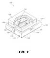
- FIG. 1is a partially cut-away perspective view of the optical device package in accordance with this disclosure
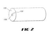
- FIG. 2is a perspective view showing an optical fiber disposed through a ferrule
- FIG. 3is a perspective view of the frame
- FIG. 4is a perspective view of the substrate and optical semiconductor component
- FIG. 5is a side view of the frame mounted to the substrate in accordance with this disclosure.
- FIG. 6is a side view of the optical device package showing the lid mounted to the structure illustrated in FIG. 5;
- FIG. 7is an exploded perspective view of an alternative embodiment of the optical device package in accordance with the disclosure.
- proximal and distalare herein used relative to each other and not to any fixed external frame of reference.
- FIGS. 1, 3 and 4illustrate an optical device package 100 having a substrate 110 in combination with an optical signal carrier, i.e., optical fiber stub 130 , a frame 120 , and optionally an optical semiconductor component 140 and a lid 150 .
- an optical signal carrieri.e., optical fiber stub 130
- a frame 120i.e., a frame 120
- an optical semiconductor component 140 and a lid 150i.e., optical semiconductor component 140 and a lid 150 .
- substrate 110can be any material suitable for providing an optical bench.
- a preferred material for fabricating substrate 110is silicon.
- Other suitable materialsinclude ceramics, polymers and metals.
- Substrate 110has a proximal end 111 , a distal end 112 , and a horizontal upper major surface 116 .
- Substrate 110is formed by etching and/or cutting or other suitable method to provide a longitudinal notch 113 for receiving the optical fiber stub 130 .
- a lateral groove 114is likewise formed for providing a vertical proximally facing stop surface 115 which is perpendicular to the direction of the optical axis of the optical fiber 130 . Stop surface 115 is also substantially perpendicular to the plane of upper surface 116 of the substrate.
- Notch 113preferably has a V-shaped cross section and is typically referred to as a “V-groove,” although other cross sectional configurations such as U-shaped cross sections (e.g., semicircular, square, rectangular, etc.) are also contemplated.
- substrate 110is single crystal silicon with the upper major surface 116 in the (100) crystallographic plane.
- the upper surface 116can be masked and selectively etched to form angled surfaces 113 a and 113 b of the V-shaped notch 113 in the (111) crystallographic planes.
- the lateral groove 114can preferably be formed by cutting the upper surface 116 with a dicing saw.
- the depth of V-shaped notch 113 and lateral groove 114can be any suitable depth for accommodating the optical fiber 130 , and illustratively may range from about 50 microns to about 500 microns.
- Optical fiber stub 130can be any conventional optical fiber and is typically from about 1 mm to about 5 mm in length, although lengths outside of this range can also be employed when suitable. Optical fiber stub 130 typically has a diameter of about 125 microns (standard). However, larger or smaller diameters can be employed when suitable.
- the optical fiber stub 130is mounted in longitudinal V-shaped notch 113 , preferably such that the distal end of the optical fiber 130 abuts and is flush against the proximally facing stop surface 115 of the lateral groove 114 . Alternatively, as shown in FIG.
- the optical fiber 130can be disposed through an axial bore 133 in ferrule 131 , the ferrule 131 being disposed between substrate 110 and frame 120 .
- the ferrule 131can be fabricated from, for example, ceramic or glass, and typically has a diameter ranging from about 1 mm to about 3 mm.
- the optical fiber 130can be secured within the axial bore of the ferrule by a bonding agent such as, for example, solder glass, epoxy resin, and the like.
- the optical semiconductor component 140is an optional component preferably mounted on the upper surface 116 of the substrate distal of the lateral groove 114 and can be any suitable semiconductor device for emitting or receiving light, such as for example, a laser diode, light emitting diode (LED), or a photodetector.
- At least one, and preferably two, electrically conductive leads 145extend from the optical semiconductor component along the upper surface 116 of substrate 110 to at least the distal edge 112 of the substrate so as to enable the optical semiconductor component to be electrically connected to a power source or various other components of an electrical circuit.
- Such optical semiconductor componentsare well known in the art.
- the electrical leads 145are preferably formed as thin films from conductive materials such as aluminum or copper by, for example, vapor deposition, or other suitable technique.
- Frame 120is an intermediate support structure preferably fabricated from a ceramic, glass, or silicon or other material which does not plastically deform at the temperatures used to process and fabricate the optical device package 100 and includes a single piece member 121 having an inner edge 122 which defines an opening 123 .
- Single piece member 121preferably has a band-like structure circumscribing the opening 123 and is preferably quadrilateral in shape although other shapes such as circular or oval are also contemplated as being within the scope of the invention.
- Frame 120further includes a recess 125 configured to accommodate the optical fiber 130 (or ferrule 131 ), and at least one, and preferably two, downwardly extending projections 124 configured to engage the respective lateral end portions of groove 114 in the substrate.
- the projections 124can be rectangular in shape to match the cross sectional configuration of groove 114 . Alternatively, other shapes can be used when deemed appropriate.
- Frame 120can be of any suitable shape or dimensions. Preferably, frame 120 has a thickness D (see, FIG. 3) ranging from about 100 microns to about 1,000 microns.
- Frame 120is fixedly bonded to the upper surface 111 of the substrate such that opening 122 is over the optical semiconductor component 140 and at least a portion of the optical fiber 130 .
- Bonding of frame 120 to substrate 110can be achieved by any suitable means such as soldering with metal, bonding with solder glass frit or BCB (benzocyclobutene resin), or adhesives such as epoxy resins, etc.
- the framecan be metallized or roughened, if necessary, to facilitate soldering or bonding.
- Solder glass fritis a low melting point glass such as, for example, borate glass, lead zinc borate glass, and the like. Generally, solder glass frit has a melting point of from about 300° C. to about 800° C., typically 325° C. to about 500° C. Solder glass frit suitable for use in the present invention is commercially available, for example, from Schott Glass Technologies of Duryea, Pa.
- the projection 124is preferably configured to at least approximately match the shape of the groove 114 . However, the match does not have to be exact. Any gap between the projection 124 and groove 114 can be occupied by a gap filling sealant 105 such as solder glass, epoxy resin, and the like, thereby providing a hermetic seal.
- the frame 120is advantageously self-aligning. That is, the frame 120 can be dropped into place onto the substrate 110 and will seat itself upon the engagement of the projections 124 with the lateral groove 114 and the engagement of the recess 125 with the optical fiber 130 . Active alignment by the manufacturer is not required.
- groove 113is configured and dimensioned such that the axial center 132 of optical fiber stub 130 , i.e., the optical axis, is aligned with the active area of the optical semiconductor component 140 .
- Thispermits optical signals to be communicated between the optical fiber 130 and the optical semiconductor component 140 .
- other componentssuch as a lens, filter, modulator, etc., can be included in the optical device package 100 and interposed between the optical fiber 130 and the optical semiconductor component 140 .
- a lid 150is preferably bonded to the frame 120 to form an enclosure. Together with frame 120 , lid 150 forms a cover structure for sealing the optical components (optical fiber stub 130 , optical semiconductor component 140 , etc.) within the enclosure.
- Lid 150can be fabricated as a flat plate from any suitable fluid impervious material such as silicon, glass, ceramic, metal, and the like. Lid 150 can be bonded to frame 120 by any suitable means such as bonding with a bonding material such as solder metal, solder glass frit, adhesives such as epoxy, BCB, and the like.
- the top surface of frame 120can optionally be metallized or roughened to facilitate adhesion of the bonding material.
- the electrical leads 145can be electrically connected to an electric circuit (not shown) by conventional means.
- the lid 150is typically bonded to frame 120 at a temperature lower than that at which the frome 120 is bonded to substrate 110 .
- Use of frame 120enables the bonding of the optical fiber 130 and the optical semiconductor component 140 to be performed in different steps at different temperatures.
- the multistep assemblyis advantageous because optical semiconductor components are generally more sensitive to higher temperatures and are subject to damage at bonding temperatures which optical fibers can readily tolerate.
- Trace 146is preferably a metal film which extends at least partially across the upper surface 116 of the substrate 110 between the optical semiconductor component 140 and an electronic component 147 for performing such functions as, for example, modifying, filtering, or switching the electrical signal to or from the optical semiconductor component 140 .
- Electronic components for performing such functionsare known in the art.
- frame 120 Ais a ceramic with internal electrical connections. The internal electrical corrections can be made by incorporating conductive metals into the frame when the ceramic material is in a malleable, unhardened state.
- the frame 120 Ais fabricated from “green sheets” of ceramic precursor such as alumina, aluminum nitride, silicon carbide, and the like.
- the green sheetsare flexible and easily processed either by cutting, punching holes in them, bending, etc.
- Conductive pastecan be applied to the sheets to form conductive paths. Holes can be filled with paste and paste can be patterned onto the sheets by silk screening and the like.
- the sheetscan be stacked, laminated and then sintered at a suitably high temperature to form a solid ceramic structure.
- Frame 120 Aalso preferably includes at least one downwardly extending projection 124 A for engaging the lateral end portion of laterally extending notch 114 and a recess 125 A for accommodating the optical fiber 130 .
- multiple optical device packagescan be made in a batch type process from a single wafer.
- the frames for the individual device packagescan be initially joined together in a multiframe network which is mounted to the wafer and aligned such that the individual frames are secured to respective individual optical device packages.
- the individual optical device packagescan be divided into separate units after assembly by means of a dicing saw or other suitable technique.
Landscapes
- Physics & Mathematics (AREA)
- General Physics & Mathematics (AREA)
- Optics & Photonics (AREA)
- Optical Couplings Of Light Guides (AREA)
Abstract
Description
- This application claims priority to U.S. provisional application Serial No. 60/250,943 filed Dec. 1, 2000.[0001]
- 1. Technical Field[0002]
- The present disclosure relates to a package for optical devices, and particularly to a module for operatively coupling one or more optical fibers with one or more optical devices.[0003]
- 2. Description of the Related Art[0004]
- Various optical devices are known in the art and include such semiconductor devices as light emitting diodes (LEDs), laser diodes, and photodetectors. Optical semiconductors, e.g., optoelectronic devices, effect a conversion between optical signals and electronic signals.[0005]
- Optical semiconductor components are sensitive to environmental conditions and are generally sealed in hermetic packages or in plastic molding to prevent degradation caused by atmospheric contaminants such as humidity, dust, and free ions. The optical input/output surfaces of the components operatively coupled in a package are especially susceptible to contamination, hence, the desirability of hermetically sealing the package to prevent contact with the outside atmosphere. Hermetic sealing typically involves mounting a cap to a substrate having an optical semiconductor component by means of soldering, welding, and the like.[0006]
- One prior known optical semiconductor module includes a submount body having a groove, an optical semiconductor component mounted on the submount body, a cap arranged across the groove and fixedly bonded to the submount body by a bonding member for hermetically sealing the module. An electrical wiring layer connected to the semiconductor device extends to the outside of the cap through the groove.[0007]
- Another optical module includes a mounting board, an optical element, and an optical fiber mounted into a longitudinal groove in the mounting board. A lateral fiber-stop groove provides a stop surface against which the end of the optical fiber is abutted. The fiber-stop groove is typically formed by means of a dicing saw.[0008]
- A problem associated with the fiber-stop groove is the increased difficulty of achieving a hermetic seal. This difficulty is overcome by the method and device disclosed herein.[0009]
- An optical device package is provided herein which comprises a substrate having an upper surface and a longitudinal notch extending from the proximal end of the substrate to a lateral groove which is at least partially defined by a proximal facing stop surface. An optical semiconductor component is mounted to the upper surface of the substrate distal to the lateral groove. An optical fiber is positioned within the longitudinal notch, the optical fiber being operatively aligned with the optical semiconductor component. Preferably, the distal end of the optical fiber abuts the proximal facing stop surface of the substrate. The optical device package further includes a frame mounted to the upper surface of the substrate, the frame having at least one downwardly extending projection that engages the lateral groove. A lid is optionally mounted to the frame so as to define an inner space wherein the optical semiconductor component and at least a portion of the optical fiber are enclosed.[0010]
- The optical device package described herein advantageously is easier to assemble while achieving a hermetic seal. The frame is self-aligning and can seat itself into proper engagement with the substrate by simply being dropped into place.[0011]
- Various embodiments are described below with reference to the drawings wherein:[0012]
- FIG. 1 is a partially cut-away perspective view of the optical device package in accordance with this disclosure;[0013]
- FIG. 2 is a perspective view showing an optical fiber disposed through a ferrule;[0014]
- FIG. 3 is a perspective view of the frame;[0015]
- FIG. 4 is a perspective view of the substrate and optical semiconductor component;[0016]
- FIG. 5 is a side view of the frame mounted to the substrate in accordance with this disclosure;[0017]
- FIG. 6 is a side view of the optical device package showing the lid mounted to the structure illustrated in FIG. 5; and[0018]
- FIG. 7 is an exploded perspective view of an alternative embodiment of the optical device package in accordance with the disclosure.[0019]
- Such terms as “proximal” and “distal”, “upper” and “lower”, “horizontal” and “vertical”, are herein used relative to each other and not to any fixed external frame of reference.[0020]
- Referring to the drawings, FIGS. 1, 3 and[0021]4 illustrate an
optical device package 100 having asubstrate 110 in combination with an optical signal carrier, i.e.,optical fiber stub 130, aframe 120, and optionally anoptical semiconductor component 140 and alid 150. - More particularly,[0022]
substrate 110 can be any material suitable for providing an optical bench. A preferred material for fabricatingsubstrate 110 is silicon. Other suitable materials include ceramics, polymers and metals.Substrate 110 has aproximal end 111, adistal end 112, and a horizontal uppermajor surface 116.Substrate 110 is formed by etching and/or cutting or other suitable method to provide alongitudinal notch 113 for receiving theoptical fiber stub 130. Alateral groove 114 is likewise formed for providing a vertical proximally facingstop surface 115 which is perpendicular to the direction of the optical axis of theoptical fiber 130.Stop surface 115 is also substantially perpendicular to the plane ofupper surface 116 of the substrate. Notch113 preferably has a V-shaped cross section and is typically referred to as a “V-groove,” although other cross sectional configurations such as U-shaped cross sections (e.g., semicircular, square, rectangular, etc.) are also contemplated. Preferably,substrate 110 is single crystal silicon with the uppermajor surface 116 in the (100) crystallographic plane. Theupper surface 116 can be masked and selectively etched to formangled surfaces shaped notch 113 in the (111) crystallographic planes. Thelateral groove 114 can preferably be formed by cutting theupper surface 116 with a dicing saw. The depth of V-shaped notch 113 andlateral groove 114 can be any suitable depth for accommodating theoptical fiber 130, and illustratively may range from about 50 microns to about 500 microns. - [0023]
Optical fiber stub 130 can be any conventional optical fiber and is typically from about 1 mm to about 5 mm in length, although lengths outside of this range can also be employed when suitable.Optical fiber stub 130 typically has a diameter of about 125 microns (standard). However, larger or smaller diameters can be employed when suitable. Theoptical fiber stub 130 is mounted in longitudinal V-shaped notch 113, preferably such that the distal end of theoptical fiber 130 abuts and is flush against the proximally facingstop surface 115 of thelateral groove 114. Alternatively, as shown in FIG. 2, theoptical fiber 130 can be disposed through anaxial bore 133 inferrule 131, theferrule 131 being disposed betweensubstrate 110 andframe 120. Theferrule 131 can be fabricated from, for example, ceramic or glass, and typically has a diameter ranging from about 1 mm to about 3 mm. Theoptical fiber 130 can be secured within the axial bore of the ferrule by a bonding agent such as, for example, solder glass, epoxy resin, and the like. - The[0024]
optical semiconductor component 140 is an optional component preferably mounted on theupper surface 116 of the substrate distal of thelateral groove 114 and can be any suitable semiconductor device for emitting or receiving light, such as for example, a laser diode, light emitting diode (LED), or a photodetector. At least one, and preferably two, electrically conductive leads145 extend from the optical semiconductor component along theupper surface 116 ofsubstrate 110 to at least thedistal edge 112 of the substrate so as to enable the optical semiconductor component to be electrically connected to a power source or various other components of an electrical circuit. Such optical semiconductor components are well known in the art. Theelectrical leads 145 are preferably formed as thin films from conductive materials such as aluminum or copper by, for example, vapor deposition, or other suitable technique. - [0025]
Frame 120 is an intermediate support structure preferably fabricated from a ceramic, glass, or silicon or other material which does not plastically deform at the temperatures used to process and fabricate theoptical device package 100 and includes asingle piece member 121 having aninner edge 122 which defines anopening 123.Single piece member 121 preferably has a band-like structure circumscribing theopening 123 and is preferably quadrilateral in shape although other shapes such as circular or oval are also contemplated as being within the scope of the invention.Frame 120 further includes arecess 125 configured to accommodate the optical fiber130 (or ferrule131), and at least one, and preferably two, downwardly extendingprojections 124 configured to engage the respective lateral end portions ofgroove 114 in the substrate. Theprojections 124 can be rectangular in shape to match the cross sectional configuration ofgroove 114. Alternatively, other shapes can be used when deemed appropriate.Frame 120 can be of any suitable shape or dimensions. Preferably,frame 120 has a thickness D (see, FIG. 3) ranging from about 100 microns to about 1,000 microns. - [0026]
Frame 120 is fixedly bonded to theupper surface 111 of the substrate such thatopening 122 is over theoptical semiconductor component 140 and at least a portion of theoptical fiber 130. Bonding offrame 120 tosubstrate 110 can be achieved by any suitable means such as soldering with metal, bonding with solder glass frit or BCB (benzocyclobutene resin), or adhesives such as epoxy resins, etc. The frame can be metallized or roughened, if necessary, to facilitate soldering or bonding. - Solder glass frit is a low melting point glass such as, for example, borate glass, lead zinc borate glass, and the like. Generally, solder glass frit has a melting point of from about 300° C. to about 800° C., typically 325° C. to about 500° C. Solder glass frit suitable for use in the present invention is commercially available, for example, from Schott Glass Technologies of Duryea, Pa.[0027]
- Referring now to FIG. 5, it can be seen that when the[0028]
frame 120 is mounted tosubstrate 110 the downwardly extendingprojection 124 engages thelateral groove 114. Theprojection 124 is preferably configured to at least approximately match the shape of thegroove 114. However, the match does not have to be exact. Any gap between theprojection 124 and groove114 can be occupied by agap filling sealant 105 such as solder glass, epoxy resin, and the like, thereby providing a hermetic seal. Theframe 120 is advantageously self-aligning. That is, theframe 120 can be dropped into place onto thesubstrate 110 and will seat itself upon the engagement of theprojections 124 with thelateral groove 114 and the engagement of therecess 125 with theoptical fiber 130. Active alignment by the manufacturer is not required. - Referring to FIG. 1, groove[0029]113 is configured and dimensioned such that the
axial center 132 ofoptical fiber stub 130, i.e., the optical axis, is aligned with the active area of theoptical semiconductor component 140. This permits optical signals to be communicated between theoptical fiber 130 and theoptical semiconductor component 140. Optionally, other components such as a lens, filter, modulator, etc., can be included in theoptical device package 100 and interposed between theoptical fiber 130 and theoptical semiconductor component 140. - Referring now to FIGS. 1 and 6, a[0030]
lid 150 is preferably bonded to theframe 120 to form an enclosure. Together withframe 120,lid 150 forms a cover structure for sealing the optical components (optical fiber stub 130,optical semiconductor component 140, etc.) within the enclosure.Lid 150 can be fabricated as a flat plate from any suitable fluid impervious material such as silicon, glass, ceramic, metal, and the like.Lid 150 can be bonded to frame120 by any suitable means such as bonding with a bonding material such as solder metal, solder glass frit, adhesives such as epoxy, BCB, and the like. The top surface offrame 120 can optionally be metallized or roughened to facilitate adhesion of the bonding material. Upon completion of assembly, theelectrical leads 145 can be electrically connected to an electric circuit (not shown) by conventional means. Thelid 150 is typically bonded to frame120 at a temperature lower than that at which the frome120 is bonded tosubstrate 110. Use offrame 120 enables the bonding of theoptical fiber 130 and theoptical semiconductor component 140 to be performed in different steps at different temperatures. The multistep assembly is advantageous because optical semiconductor components are generally more sensitive to higher temperatures and are subject to damage at bonding temperatures which optical fibers can readily tolerate. - Referring now to FIG. 7, in an[0031]
alternative embodiment 100A of the optical device package includes electrical connections such asconductive metal trace 146.Trace 146 is preferably a metal film which extends at least partially across theupper surface 116 of thesubstrate 110 between theoptical semiconductor component 140 and anelectronic component 147 for performing such functions as, for example, modifying, filtering, or switching the electrical signal to or from theoptical semiconductor component 140. Electronic components for performing such functions are known in the art. Preferably frame120A is a ceramic with internal electrical connections. The internal electrical corrections can be made by incorporating conductive metals into the frame when the ceramic material is in a malleable, unhardened state. For example, in a preferred method, theframe 120A is fabricated from “green sheets” of ceramic precursor such as alumina, aluminum nitride, silicon carbide, and the like. The green sheets are flexible and easily processed either by cutting, punching holes in them, bending, etc. Conductive paste can be applied to the sheets to form conductive paths. Holes can be filled with paste and paste can be patterned onto the sheets by silk screening and the like. The sheets can be stacked, laminated and then sintered at a suitably high temperature to form a solid ceramic structure.Frame 120A also preferably includes at least one downwardly extendingprojection 124A for engaging the lateral end portion of laterally extendingnotch 114 and a recess125A for accommodating theoptical fiber 130. - Incorporation of electrical connecting lines such as[0032]
metal trace 146 in the frame allows the electrical connection to bridgelateral groove 114. This feature provides more efficient use of valuable surface area within the optical device package by permitting electronic components (e.g. component147) to be positioned on theupper surface 116 proximal to thelateral groove 114 and to be electrically connected tooptical semiconductor component 140 positioned on theupper surface 116 distal to thelateral groove 114. - While the above description contains many specifics, these specifics should not be construed as limitations on the scope of the invention, but merely as exemplifications of preferred embodiments thereof. For example, multiple optical device packages can be made in a batch type process from a single wafer. The frames for the individual device packages can be initially joined together in a multiframe network which is mounted to the wafer and aligned such that the individual frames are secured to respective individual optical device packages. The individual optical device packages can be divided into separate units after assembly by means of a dicing saw or other suitable technique. Those skilled in the art will envision many other possibilities within the scope and spirit of the invention as defined by the claims appended hereto.[0033]
Claims (22)
Priority Applications (1)
| Application Number | Priority Date | Filing Date | Title |
|---|---|---|---|
| US09/990,509US6827503B2 (en) | 2000-12-01 | 2001-11-21 | Optical device package having a configured frame |
Applications Claiming Priority (2)
| Application Number | Priority Date | Filing Date | Title |
|---|---|---|---|
| US25094300P | 2000-12-01 | 2000-12-01 | |
| US09/990,509US6827503B2 (en) | 2000-12-01 | 2001-11-21 | Optical device package having a configured frame |
Publications (2)
| Publication Number | Publication Date |
|---|---|
| US20030123816A1true US20030123816A1 (en) | 2003-07-03 |
| US6827503B2 US6827503B2 (en) | 2004-12-07 |
Family
ID=26941261
Family Applications (1)
| Application Number | Title | Priority Date | Filing Date |
|---|---|---|---|
| US09/990,509Expired - Fee RelatedUS6827503B2 (en) | 2000-12-01 | 2001-11-21 | Optical device package having a configured frame |
Country Status (1)
| Country | Link |
|---|---|
| US (1) | US6827503B2 (en) |
Cited By (10)
| Publication number | Priority date | Publication date | Assignee | Title |
|---|---|---|---|---|
| US20020090180A1 (en)* | 2001-01-10 | 2002-07-11 | Kia Silverbrook | Wafer scale fiber optic termination |
| US20030095759A1 (en)* | 2000-12-14 | 2003-05-22 | Dautartas Mindaugas F. | Optical device package for flip-chip mounting |
| US6811853B1 (en) | 2000-03-06 | 2004-11-02 | Shipley Company, L.L.C. | Single mask lithographic process for patterning multiple types of surface features |
| US20040264866A1 (en)* | 2000-10-25 | 2004-12-30 | Sherrer David W. | Wafer level packaging for optoelectronic devices |
| US20050127384A1 (en)* | 2003-12-12 | 2005-06-16 | Hitachi., Ltd. | Semiconductor optical devices and optical modules |
| US20050139644A1 (en)* | 2003-12-22 | 2005-06-30 | Rohm And Haas Electronic Materials Llc | Electronic devices and methods of forming electronic devices |
| US6932519B2 (en) | 2000-11-16 | 2005-08-23 | Shipley Company, L.L.C. | Optical device package |
| US20060262820A1 (en)* | 2005-05-18 | 2006-11-23 | Sharp Kabushiki Kaisha | Semiconductor laser device and optical pickup apparatus having the device |
| US20150355420A1 (en)* | 2012-03-05 | 2015-12-10 | Nanoprecision Products, Inc. | Coupling device having a stamped structured surface for routing optical data signals |
| GB2567047A (en)* | 2017-08-07 | 2019-04-03 | Rockley Photonics Ltd | Optoelectronic module package |
Families Citing this family (6)
| Publication number | Priority date | Publication date | Assignee | Title |
|---|---|---|---|---|
| US20020136507A1 (en)* | 2001-02-26 | 2002-09-26 | Musk Robert W. | Laser welding components to an optical micro-bench |
| US7450862B2 (en)* | 2002-03-19 | 2008-11-11 | Axsun Technologies, Inc. | Stray light insensitive detector system and amplifier |
| US7794158B2 (en)* | 2007-10-04 | 2010-09-14 | Hitachi Cable Ltd. | Fabrication method of optical interconnection component and optical interconnection component itself |
| CN101877318B (en)* | 2009-04-30 | 2012-02-29 | 赫克斯科技股份有限公司 | Frame type ceramic copper clad laminate and manufacturing method thereof |
| WO2012097513A1 (en)* | 2011-01-20 | 2012-07-26 | 青岛海信宽带多媒体技术有限公司 | Photoelectric chip module and encapsulation method |
| US8876410B2 (en) | 2012-01-11 | 2014-11-04 | Cisco Technology, Inc. | Self-aligning connectorized fiber array assembly |
Citations (56)
| Publication number | Priority date | Publication date | Assignee | Title |
|---|---|---|---|---|
| US81914A (en)* | 1868-09-08 | James l | ||
| US95759A (en)* | 1869-10-12 | benoit | ||
| US3404215A (en)* | 1966-04-14 | 1968-10-01 | Sprague Electric Co | Hermetically sealed electronic module |
| US3768991A (en)* | 1972-06-14 | 1973-10-30 | Diacon | Method for sealing an enclosure for an electronic component |
| US3874549A (en)* | 1972-05-26 | 1975-04-01 | Norman Hascoe | Hermetic sealing cover for a container for a semiconductor device |
| US4038157A (en)* | 1976-04-16 | 1977-07-26 | The United States Of America As Represented By The Secretary Of The Air Force | Method of hermetically sealing semiconductor devices |
| US4065203A (en)* | 1975-12-10 | 1977-12-27 | International Telephone And Telegraph Corporation | Couplers for electro-optical elements |
| US4199222A (en)* | 1976-11-12 | 1980-04-22 | Hitachi, Ltd. | Optical device with a laser-to-fiber coupler |
| US4210923A (en)* | 1979-01-02 | 1980-07-01 | Bell Telephone Laboratories, Incorporated | Edge illuminated photodetector with optical fiber alignment |
| US4270134A (en)* | 1978-04-28 | 1981-05-26 | Hitachi, Ltd. | Light-emitting semiconductor device |
| US4411057A (en)* | 1978-05-18 | 1983-10-25 | Thomson-Csf | Method of manufacturing a laser source with stamped support |
| US4791075A (en)* | 1987-10-05 | 1988-12-13 | Motorola, Inc. | Process for making a hermetic low cost pin grid array package |
| US4802952A (en)* | 1987-03-06 | 1989-02-07 | Hitachi, Ltd. | Method for manufacturing semiconductor absolute pressure sensor units |
| US4826272A (en)* | 1987-08-27 | 1989-05-02 | American Telephone And Telegraph Company At&T Bell Laboratories | Means for coupling an optical fiber to an opto-electronic device |
| US4897711A (en)* | 1988-03-03 | 1990-01-30 | American Telephone And Telegraph Company | Subassembly for optoelectronic devices |
| US4904036A (en)* | 1988-03-03 | 1990-02-27 | American Telephone And Telegraph Company, At&T Bell Laboratories | Subassemblies for optoelectronic hybrid integrated circuits |
| US4907065A (en)* | 1988-03-01 | 1990-03-06 | Lsi Logic Corporation | Integrated circuit chip sealing assembly |
| US5071213A (en)* | 1990-10-31 | 1991-12-10 | The Boeing Company | Optical coupler and method of making optical coupler |
| US5313546A (en)* | 1991-11-29 | 1994-05-17 | Sirti, S.P.A. | Hermetically sealed joint cover for fibre optic cables |
| US5323051A (en)* | 1991-12-16 | 1994-06-21 | Motorola, Inc. | Semiconductor wafer level package |
| US5384872A (en)* | 1992-02-14 | 1995-01-24 | Lucas Industries Public Limited Company | Optical device and a method of manufacture thereof |
| US5412748A (en)* | 1992-12-04 | 1995-05-02 | Kabushiki Kaisha Toshiba | Optical semiconductor module |
| US5448014A (en)* | 1993-01-27 | 1995-09-05 | Trw Inc. | Mass simultaneous sealing and electrical connection of electronic devices |
| US5454005A (en)* | 1993-01-13 | 1995-09-26 | Omnipoint Corporation | Reciprocal mode saw correlator method and apparatus |
| US5478778A (en)* | 1991-08-30 | 1995-12-26 | Nec Corporation | Method of manufacturing a compact optical semiconductor module capable of being readily assembled with a high precision |
| US5504372A (en)* | 1992-08-21 | 1996-04-02 | Olin Corporation | Adhesively sealed metal electronic package incorporating a multi-chip module |
| US5550398A (en)* | 1994-10-31 | 1996-08-27 | Texas Instruments Incorporated | Hermetic packaging with optical |
| US5562837A (en)* | 1994-02-10 | 1996-10-08 | Matra Marconi Space France | Method for connecting electronic circuits in a multi-chip module having a co-fired substrate and multi-chip module obtained thereby |
| US5604160A (en)* | 1996-07-29 | 1997-02-18 | Motorola, Inc. | Method for packaging semiconductor devices |
| US5671315A (en)* | 1994-03-09 | 1997-09-23 | Fujitsu Limited | Optical parts fixing apparatus and method of manufacturing the same |
| US5798557A (en)* | 1996-08-29 | 1998-08-25 | Harris Corporation | Lid wafer bond packaging and micromachining |
| US5818404A (en)* | 1996-03-04 | 1998-10-06 | Motorola, Inc. | Integrated electro-optical package |
| US5960141A (en)* | 1997-10-17 | 1999-09-28 | Fujitsu Limited | Optical transmission terminal device |
| US6056448A (en)* | 1998-04-16 | 2000-05-02 | Lockheed Martin Corporation | Vertical cavity surface emitting laser array packaging |
| US6106735A (en)* | 1997-01-11 | 2000-08-22 | Robert Bosch Gmbh | Wafer stack and method of producing sensors |
| US6207950B1 (en)* | 1999-01-11 | 2001-03-27 | Lightlogic, Inc. | Optical electronic assembly having a flexure for maintaining alignment between optical elements |
| US6222967B1 (en)* | 1997-03-13 | 2001-04-24 | Nippon Telegraph And Telephone Corporation | Packaging platform, optical module using the platform, and methods for producing the platform and the module |
| US6228675B1 (en)* | 1999-07-23 | 2001-05-08 | Agilent Technologies, Inc. | Microcap wafer-level package with vias |
| US20010022382A1 (en)* | 1998-07-29 | 2001-09-20 | Shook James Gill | Method of and apparatus for sealing an hermetic lid to a semiconductor die |
| US6318910B1 (en)* | 1997-04-18 | 2001-11-20 | Nec Corporation | Method for hermetically sealing optical fiber introducing section and hermetically sealed structure |
| US20020001435A1 (en)* | 2000-06-28 | 2002-01-03 | Steinberg Dan A. | Method for cleaving integrated optic waveguides to provide a smooth waveguide endface |
| US6377742B1 (en)* | 1998-03-16 | 2002-04-23 | Sumitomo Electric Industries, Ltd. | Lead frame, optical module, and a method of optical module |
| US20020090749A1 (en)* | 2001-01-09 | 2002-07-11 | 3M Innovative Properties Company | Hermetic package for mems devices with integrated carrier |
| US20020113296A1 (en)* | 2001-02-03 | 2002-08-22 | Samsung Electronics Co., Ltd. | Wafer level hermetic sealing method |
| US20030007771A1 (en)* | 2001-02-08 | 2003-01-09 | Steinberg Dan A. | Method and device for passively locating a fiber stub in a groove |
| US20030034438A1 (en)* | 1998-11-25 | 2003-02-20 | Sherrer David W. | Optoelectronic device-optical fiber connector having micromachined pit for passive alignment of the optoelectronic device |
| US20030071283A1 (en)* | 2001-10-17 | 2003-04-17 | Hymite A/S | Semiconductor structure with one or more through-holes |
| US20030081914A1 (en)* | 2000-11-16 | 2003-05-01 | Steinberg Dan A. | Optical device package |
| US20030095759A1 (en)* | 2000-12-14 | 2003-05-22 | Dautartas Mindaugas F. | Optical device package for flip-chip mounting |
| US6585426B2 (en)* | 2000-01-18 | 2003-07-01 | Nippon Telegraph And Telephone Corporation | Optical module using wiring lead integrated resin substrate |
| US20030123833A1 (en)* | 2000-10-16 | 2003-07-03 | Neal Ricks | Embedded waveguide with alignment grooves and method for making same |
| US20030137022A1 (en)* | 2001-01-31 | 2003-07-24 | Dautartas Mindaugas F. | Optoelectronic submount having an on-edge optoelectronic device |
| US6611001B2 (en)* | 2001-02-06 | 2003-08-26 | Lucent Technologies Inc. | Laser package |
| US6632027B1 (en)* | 1998-08-01 | 2003-10-14 | Hitachi, Ltd. | Optical module |
| US6655853B1 (en)* | 2000-08-25 | 2003-12-02 | Hrl Laboratories, Llc | Optical bond-wire interconnections and a method for fabrication thereof |
| US6680491B2 (en)* | 2000-02-01 | 2004-01-20 | Matsushita Electric Industrial Co., Ltd. | Optical electronic apparatus and method for producing the same |
Family Cites Families (3)
| Publication number | Priority date | Publication date | Assignee | Title |
|---|---|---|---|---|
| DE4232608C2 (en) | 1992-09-29 | 1994-10-06 | Bosch Gmbh Robert | Method for manufacturing a cover for an integrated optical circuit |
| US5475778A (en) | 1993-10-21 | 1995-12-12 | Motorola, Inc. | Smart optical coupler and smart optical coupler system |
| JPH0829638A (en)* | 1994-05-12 | 1996-02-02 | Fujitsu Ltd | Optical waveguide / optical fiber connection structure, optical waveguide / optical fiber connection method, optical waveguide substrate used for optical waveguide / optical fiber connection, method of manufacturing the same, and optical fiber with optical fiber substrate used for optical waveguide / optical fiber connection fiber |
- 2001
- 2001-11-21USUS09/990,509patent/US6827503B2/ennot_activeExpired - Fee Related
Patent Citations (57)
| Publication number | Priority date | Publication date | Assignee | Title |
|---|---|---|---|---|
| US81914A (en)* | 1868-09-08 | James l | ||
| US95759A (en)* | 1869-10-12 | benoit | ||
| US3404215A (en)* | 1966-04-14 | 1968-10-01 | Sprague Electric Co | Hermetically sealed electronic module |
| US3874549A (en)* | 1972-05-26 | 1975-04-01 | Norman Hascoe | Hermetic sealing cover for a container for a semiconductor device |
| US3768991A (en)* | 1972-06-14 | 1973-10-30 | Diacon | Method for sealing an enclosure for an electronic component |
| US4065203A (en)* | 1975-12-10 | 1977-12-27 | International Telephone And Telegraph Corporation | Couplers for electro-optical elements |
| US4038157A (en)* | 1976-04-16 | 1977-07-26 | The United States Of America As Represented By The Secretary Of The Air Force | Method of hermetically sealing semiconductor devices |
| US4199222A (en)* | 1976-11-12 | 1980-04-22 | Hitachi, Ltd. | Optical device with a laser-to-fiber coupler |
| US4270134A (en)* | 1978-04-28 | 1981-05-26 | Hitachi, Ltd. | Light-emitting semiconductor device |
| US4411057A (en)* | 1978-05-18 | 1983-10-25 | Thomson-Csf | Method of manufacturing a laser source with stamped support |
| US4210923A (en)* | 1979-01-02 | 1980-07-01 | Bell Telephone Laboratories, Incorporated | Edge illuminated photodetector with optical fiber alignment |
| US4802952A (en)* | 1987-03-06 | 1989-02-07 | Hitachi, Ltd. | Method for manufacturing semiconductor absolute pressure sensor units |
| US4826272A (en)* | 1987-08-27 | 1989-05-02 | American Telephone And Telegraph Company At&T Bell Laboratories | Means for coupling an optical fiber to an opto-electronic device |
| US4791075A (en)* | 1987-10-05 | 1988-12-13 | Motorola, Inc. | Process for making a hermetic low cost pin grid array package |
| US4907065A (en)* | 1988-03-01 | 1990-03-06 | Lsi Logic Corporation | Integrated circuit chip sealing assembly |
| US4897711A (en)* | 1988-03-03 | 1990-01-30 | American Telephone And Telegraph Company | Subassembly for optoelectronic devices |
| US4904036A (en)* | 1988-03-03 | 1990-02-27 | American Telephone And Telegraph Company, At&T Bell Laboratories | Subassemblies for optoelectronic hybrid integrated circuits |
| US5071213A (en)* | 1990-10-31 | 1991-12-10 | The Boeing Company | Optical coupler and method of making optical coupler |
| US5478778A (en)* | 1991-08-30 | 1995-12-26 | Nec Corporation | Method of manufacturing a compact optical semiconductor module capable of being readily assembled with a high precision |
| US5313546A (en)* | 1991-11-29 | 1994-05-17 | Sirti, S.P.A. | Hermetically sealed joint cover for fibre optic cables |
| US5323051A (en)* | 1991-12-16 | 1994-06-21 | Motorola, Inc. | Semiconductor wafer level package |
| US5384872A (en)* | 1992-02-14 | 1995-01-24 | Lucas Industries Public Limited Company | Optical device and a method of manufacture thereof |
| US5504372A (en)* | 1992-08-21 | 1996-04-02 | Olin Corporation | Adhesively sealed metal electronic package incorporating a multi-chip module |
| US5412748A (en)* | 1992-12-04 | 1995-05-02 | Kabushiki Kaisha Toshiba | Optical semiconductor module |
| US5454005A (en)* | 1993-01-13 | 1995-09-26 | Omnipoint Corporation | Reciprocal mode saw correlator method and apparatus |
| US5448014A (en)* | 1993-01-27 | 1995-09-05 | Trw Inc. | Mass simultaneous sealing and electrical connection of electronic devices |
| US5562837A (en)* | 1994-02-10 | 1996-10-08 | Matra Marconi Space France | Method for connecting electronic circuits in a multi-chip module having a co-fired substrate and multi-chip module obtained thereby |
| US5671315A (en)* | 1994-03-09 | 1997-09-23 | Fujitsu Limited | Optical parts fixing apparatus and method of manufacturing the same |
| US5550398A (en)* | 1994-10-31 | 1996-08-27 | Texas Instruments Incorporated | Hermetic packaging with optical |
| US5818404A (en)* | 1996-03-04 | 1998-10-06 | Motorola, Inc. | Integrated electro-optical package |
| US5604160A (en)* | 1996-07-29 | 1997-02-18 | Motorola, Inc. | Method for packaging semiconductor devices |
| US5798557A (en)* | 1996-08-29 | 1998-08-25 | Harris Corporation | Lid wafer bond packaging and micromachining |
| US5915168A (en)* | 1996-08-29 | 1999-06-22 | Harris Corporation | Lid wafer bond packaging and micromachining |
| US6106735A (en)* | 1997-01-11 | 2000-08-22 | Robert Bosch Gmbh | Wafer stack and method of producing sensors |
| US6222967B1 (en)* | 1997-03-13 | 2001-04-24 | Nippon Telegraph And Telephone Corporation | Packaging platform, optical module using the platform, and methods for producing the platform and the module |
| US6318910B1 (en)* | 1997-04-18 | 2001-11-20 | Nec Corporation | Method for hermetically sealing optical fiber introducing section and hermetically sealed structure |
| US5960141A (en)* | 1997-10-17 | 1999-09-28 | Fujitsu Limited | Optical transmission terminal device |
| US6377742B1 (en)* | 1998-03-16 | 2002-04-23 | Sumitomo Electric Industries, Ltd. | Lead frame, optical module, and a method of optical module |
| US6056448A (en)* | 1998-04-16 | 2000-05-02 | Lockheed Martin Corporation | Vertical cavity surface emitting laser array packaging |
| US20010022382A1 (en)* | 1998-07-29 | 2001-09-20 | Shook James Gill | Method of and apparatus for sealing an hermetic lid to a semiconductor die |
| US6632027B1 (en)* | 1998-08-01 | 2003-10-14 | Hitachi, Ltd. | Optical module |
| US20030034438A1 (en)* | 1998-11-25 | 2003-02-20 | Sherrer David W. | Optoelectronic device-optical fiber connector having micromachined pit for passive alignment of the optoelectronic device |
| US6207950B1 (en)* | 1999-01-11 | 2001-03-27 | Lightlogic, Inc. | Optical electronic assembly having a flexure for maintaining alignment between optical elements |
| US6228675B1 (en)* | 1999-07-23 | 2001-05-08 | Agilent Technologies, Inc. | Microcap wafer-level package with vias |
| US6585426B2 (en)* | 2000-01-18 | 2003-07-01 | Nippon Telegraph And Telephone Corporation | Optical module using wiring lead integrated resin substrate |
| US6680491B2 (en)* | 2000-02-01 | 2004-01-20 | Matsushita Electric Industrial Co., Ltd. | Optical electronic apparatus and method for producing the same |
| US20020001435A1 (en)* | 2000-06-28 | 2002-01-03 | Steinberg Dan A. | Method for cleaving integrated optic waveguides to provide a smooth waveguide endface |
| US6655853B1 (en)* | 2000-08-25 | 2003-12-02 | Hrl Laboratories, Llc | Optical bond-wire interconnections and a method for fabrication thereof |
| US20030123833A1 (en)* | 2000-10-16 | 2003-07-03 | Neal Ricks | Embedded waveguide with alignment grooves and method for making same |
| US20030081914A1 (en)* | 2000-11-16 | 2003-05-01 | Steinberg Dan A. | Optical device package |
| US20030095759A1 (en)* | 2000-12-14 | 2003-05-22 | Dautartas Mindaugas F. | Optical device package for flip-chip mounting |
| US20020090749A1 (en)* | 2001-01-09 | 2002-07-11 | 3M Innovative Properties Company | Hermetic package for mems devices with integrated carrier |
| US20030137022A1 (en)* | 2001-01-31 | 2003-07-24 | Dautartas Mindaugas F. | Optoelectronic submount having an on-edge optoelectronic device |
| US20020113296A1 (en)* | 2001-02-03 | 2002-08-22 | Samsung Electronics Co., Ltd. | Wafer level hermetic sealing method |
| US6611001B2 (en)* | 2001-02-06 | 2003-08-26 | Lucent Technologies Inc. | Laser package |
| US20030007771A1 (en)* | 2001-02-08 | 2003-01-09 | Steinberg Dan A. | Method and device for passively locating a fiber stub in a groove |
| US20030071283A1 (en)* | 2001-10-17 | 2003-04-17 | Hymite A/S | Semiconductor structure with one or more through-holes |
Cited By (17)
| Publication number | Priority date | Publication date | Assignee | Title |
|---|---|---|---|---|
| US6811853B1 (en) | 2000-03-06 | 2004-11-02 | Shipley Company, L.L.C. | Single mask lithographic process for patterning multiple types of surface features |
| US20040264866A1 (en)* | 2000-10-25 | 2004-12-30 | Sherrer David W. | Wafer level packaging for optoelectronic devices |
| US7345316B2 (en) | 2000-10-25 | 2008-03-18 | Shipley Company, L.L.C. | Wafer level packaging for optoelectronic devices |
| US6932519B2 (en) | 2000-11-16 | 2005-08-23 | Shipley Company, L.L.C. | Optical device package |
| US20030095759A1 (en)* | 2000-12-14 | 2003-05-22 | Dautartas Mindaugas F. | Optical device package for flip-chip mounting |
| US6883977B2 (en)* | 2000-12-14 | 2005-04-26 | Shipley Company, L.L.C. | Optical device package for flip-chip mounting |
| US20020090180A1 (en)* | 2001-01-10 | 2002-07-11 | Kia Silverbrook | Wafer scale fiber optic termination |
| US7038233B2 (en)* | 2003-12-12 | 2006-05-02 | Hitachi, Ltd. | Semiconductor optical devices and optical modules |
| US20050127384A1 (en)* | 2003-12-12 | 2005-06-16 | Hitachi., Ltd. | Semiconductor optical devices and optical modules |
| US20050139644A1 (en)* | 2003-12-22 | 2005-06-30 | Rohm And Haas Electronic Materials Llc | Electronic devices and methods of forming electronic devices |
| CN100471364C (en)* | 2003-12-22 | 2009-03-18 | 罗姆和哈斯电子材料有限责任公司 | Electronic device and method of forming electronic device |
| US20060262820A1 (en)* | 2005-05-18 | 2006-11-23 | Sharp Kabushiki Kaisha | Semiconductor laser device and optical pickup apparatus having the device |
| CN100414792C (en)* | 2005-05-18 | 2008-08-27 | 夏普株式会社 | Semiconductor laser device and optical pickup device having same |
| US20150355420A1 (en)* | 2012-03-05 | 2015-12-10 | Nanoprecision Products, Inc. | Coupling device having a stamped structured surface for routing optical data signals |
| GB2567047A (en)* | 2017-08-07 | 2019-04-03 | Rockley Photonics Ltd | Optoelectronic module package |
| GB2567047B (en)* | 2017-08-07 | 2021-12-01 | Rockley Photonics Ltd | Optoelectronic module package |
| US11239377B2 (en) | 2017-08-07 | 2022-02-01 | Rockley Photonics Limited | Optoelectronic module package |
Also Published As
| Publication number | Publication date |
|---|---|
| US6827503B2 (en) | 2004-12-07 |
Similar Documents
| Publication | Publication Date | Title |
|---|---|---|
| US6932519B2 (en) | Optical device package | |
| US6827503B2 (en) | Optical device package having a configured frame | |
| US6883977B2 (en) | Optical device package for flip-chip mounting | |
| US7345316B2 (en) | Wafer level packaging for optoelectronic devices | |
| US6786654B2 (en) | Encapsulated optical fiber end-coupled device | |
| US8233757B2 (en) | Wafer based optical chassis and associated methods | |
| US7232263B2 (en) | Optical communications module and substrate for the same | |
| US7961989B2 (en) | Optical chassis, camera having an optical chassis, and associated methods | |
| US7138661B2 (en) | Optoelectronic component and optoelectronic arrangement with an optoelectronic component | |
| JP2005038956A (en) | Optical component and manufacturing method thereof | |
| US7207729B2 (en) | TO-can having a leadframe | |
| JP2022126893A (en) | Optical module and manufacturing method of the same | |
| JP4728625B2 (en) | Optical semiconductor device and optical module using the same | |
| US5937125A (en) | Detachable fiber optic connector with improved optical sub-assembly and nose block | |
| JPS60180183A (en) | Hermetically sealing package for optical semiconductor element | |
| US7255494B2 (en) | Low-profile package for housing an optoelectronic assembly | |
| JPH059689Y2 (en) | ||
| JPH10213723A (en) | Optical semiconductor module and manufacturing method thereof | |
| CA2523418C (en) | Package for optoelectronic device on wafer level and associated methods | |
| JP3481016B2 (en) | Terminal for optical fiber array and terminal for optical fiber array equipped with optical semiconductor chip array | |
| JP2003222767A (en) | Package for storing optical semiconductor elements |
Legal Events
| Date | Code | Title | Description |
|---|---|---|---|
| AS | Assignment | Owner name:HALEOS, INC., VIRGINIA Free format text:ASSIGNMENT OF ASSIGNORS INTEREST;ASSIGNORS:STEINBERG, DAN A.;HUGHES, WILLIAM T.;DAUTARTAS, MINDAUGAS F.;AND OTHERS;REEL/FRAME:013174/0328;SIGNING DATES FROM 20020910 TO 20020920 Owner name:SHIPLEY COMPANY, L.L.C., MASSACHUSETTS Free format text:ASSIGNMENT OF ASSIGNORS INTEREST;ASSIGNOR:HALEOS, INC.;REEL/FRAME:013181/0159 Effective date:20020911 Owner name:HALEOS, INC., VIRGINIA Free format text:ASSIGNMENT OF ASSIGNORS INTEREST;ASSIGNORS:STEINBERG, DAN A.;HUGHES, WILLIAM T.;DAUTARTAS, MINDAUGAS F.;AND OTHERS;SIGNING DATES FROM 20020910 TO 20020920;REEL/FRAME:013174/0328 | |
| FPAY | Fee payment | Year of fee payment:4 | |
| REMI | Maintenance fee reminder mailed | ||
| FEPP | Fee payment procedure | Free format text:PAYOR NUMBER ASSIGNED (ORIGINAL EVENT CODE: ASPN); ENTITY STATUS OF PATENT OWNER: LARGE ENTITY Free format text:PAYER NUMBER DE-ASSIGNED (ORIGINAL EVENT CODE: RMPN); ENTITY STATUS OF PATENT OWNER: LARGE ENTITY | |
| AS | Assignment | Owner name:NUVOTRONICS, LLC,VIRGINIA Free format text:ASSIGNMENT OF ASSIGNORS INTEREST;ASSIGNOR:ROHM AND HAAS ELECTRONIC MATERIALS LLC;REEL/FRAME:024571/0939 Effective date:20080708 Owner name:NUVOTRONICS, LLC, VIRGINIA Free format text:ASSIGNMENT OF ASSIGNORS INTEREST;ASSIGNOR:ROHM AND HAAS ELECTRONIC MATERIALS LLC;REEL/FRAME:024571/0939 Effective date:20080708 | |
| AS | Assignment | Owner name:IP CUBE PARTNERS CO. LTD., KOREA, REPUBLIC OF Free format text:ASSIGNMENT OF ASSIGNORS INTEREST;ASSIGNOR:NUVOTRONICS, LLC;REEL/FRAME:025950/0153 Effective date:20100831 | |
| AS | Assignment | Owner name:SAMSUNG ELECTRONICS CO., LTD., KOREA, REPUBLIC OF Free format text:ASSIGNMENT OF ASSIGNORS INTEREST;ASSIGNOR:IP CUBE PARTNERS CO. LTD.;REEL/FRAME:026323/0651 Effective date:20110512 | |
| FPAY | Fee payment | Year of fee payment:8 | |
| REMI | Maintenance fee reminder mailed | ||
| LAPS | Lapse for failure to pay maintenance fees | ||
| STCH | Information on status: patent discontinuation | Free format text:PATENT EXPIRED DUE TO NONPAYMENT OF MAINTENANCE FEES UNDER 37 CFR 1.362 | |
| FP | Lapsed due to failure to pay maintenance fee | Effective date:20161207 |