US20030123513A1 - Assymmetric distributed bragg reflector for vertical cavity surface emitting lasers - Google Patents
Assymmetric distributed bragg reflector for vertical cavity surface emitting lasersDownload PDFInfo
- Publication number
- US20030123513A1 US20030123513A1US10/028,435US2843501AUS2003123513A1US 20030123513 A1US20030123513 A1US 20030123513A1US 2843501 AUS2843501 AUS 2843501AUS 2003123513 A1US2003123513 A1US 2003123513A1
- Authority
- US
- United States
- Prior art keywords
- mirror
- transition
- doped
- region
- semiconductor layer
- Prior art date
- Legal status (The legal status is an assumption and is not a legal conclusion. Google has not performed a legal analysis and makes no representation as to the accuracy of the status listed.)
- Granted
Links
Images


Classifications
- H—ELECTRICITY
- H01—ELECTRIC ELEMENTS
- H01S—DEVICES USING THE PROCESS OF LIGHT AMPLIFICATION BY STIMULATED EMISSION OF RADIATION [LASER] TO AMPLIFY OR GENERATE LIGHT; DEVICES USING STIMULATED EMISSION OF ELECTROMAGNETIC RADIATION IN WAVE RANGES OTHER THAN OPTICAL
- H01S5/00—Semiconductor lasers
- H01S5/10—Construction or shape of the optical resonator, e.g. extended or external cavity, coupled cavities, bent-guide, varying width, thickness or composition of the active region
- H01S5/12—Construction or shape of the optical resonator, e.g. extended or external cavity, coupled cavities, bent-guide, varying width, thickness or composition of the active region the resonator having a periodic structure, e.g. in distributed feedback [DFB] lasers
- H01S5/125—Distributed Bragg reflector [DBR] lasers
- H—ELECTRICITY
- H01—ELECTRIC ELEMENTS
- H01S—DEVICES USING THE PROCESS OF LIGHT AMPLIFICATION BY STIMULATED EMISSION OF RADIATION [LASER] TO AMPLIFY OR GENERATE LIGHT; DEVICES USING STIMULATED EMISSION OF ELECTROMAGNETIC RADIATION IN WAVE RANGES OTHER THAN OPTICAL
- H01S5/00—Semiconductor lasers
- H01S5/10—Construction or shape of the optical resonator, e.g. extended or external cavity, coupled cavities, bent-guide, varying width, thickness or composition of the active region
- H01S5/18—Surface-emitting [SE] lasers, e.g. having both horizontal and vertical cavities
- H01S5/183—Surface-emitting [SE] lasers, e.g. having both horizontal and vertical cavities having only vertical cavities, e.g. vertical cavity surface-emitting lasers [VCSEL]
- H01S5/18308—Surface-emitting [SE] lasers, e.g. having both horizontal and vertical cavities having only vertical cavities, e.g. vertical cavity surface-emitting lasers [VCSEL] having a special structure for lateral current or light confinement
- H01S5/18311—Surface-emitting [SE] lasers, e.g. having both horizontal and vertical cavities having only vertical cavities, e.g. vertical cavity surface-emitting lasers [VCSEL] having a special structure for lateral current or light confinement using selective oxidation
- H01S5/18313—Surface-emitting [SE] lasers, e.g. having both horizontal and vertical cavities having only vertical cavities, e.g. vertical cavity surface-emitting lasers [VCSEL] having a special structure for lateral current or light confinement using selective oxidation by oxidizing at least one of the DBR layers
- H—ELECTRICITY
- H01—ELECTRIC ELEMENTS
- H01S—DEVICES USING THE PROCESS OF LIGHT AMPLIFICATION BY STIMULATED EMISSION OF RADIATION [LASER] TO AMPLIFY OR GENERATE LIGHT; DEVICES USING STIMULATED EMISSION OF ELECTROMAGNETIC RADIATION IN WAVE RANGES OTHER THAN OPTICAL
- H01S5/00—Semiconductor lasers
- H01S5/10—Construction or shape of the optical resonator, e.g. extended or external cavity, coupled cavities, bent-guide, varying width, thickness or composition of the active region
- H01S5/18—Surface-emitting [SE] lasers, e.g. having both horizontal and vertical cavities
- H01S5/183—Surface-emitting [SE] lasers, e.g. having both horizontal and vertical cavities having only vertical cavities, e.g. vertical cavity surface-emitting lasers [VCSEL]
- H01S5/18358—Surface-emitting [SE] lasers, e.g. having both horizontal and vertical cavities having only vertical cavities, e.g. vertical cavity surface-emitting lasers [VCSEL] containing spacer layers to adjust the phase of the light wave in the cavity
- H—ELECTRICITY
- H01—ELECTRIC ELEMENTS
- H01S—DEVICES USING THE PROCESS OF LIGHT AMPLIFICATION BY STIMULATED EMISSION OF RADIATION [LASER] TO AMPLIFY OR GENERATE LIGHT; DEVICES USING STIMULATED EMISSION OF ELECTROMAGNETIC RADIATION IN WAVE RANGES OTHER THAN OPTICAL
- H01S5/00—Semiconductor lasers
- H01S5/30—Structure or shape of the active region; Materials used for the active region
- H01S5/305—Structure or shape of the active region; Materials used for the active region characterised by the doping materials used in the laser structure
- H01S5/3054—Structure or shape of the active region; Materials used for the active region characterised by the doping materials used in the laser structure p-doping
Definitions
- the present inventionrelates to laser mirror structures. More specifically, it relates to mirror structures suitable for use in vertical cavity surface emitting lasers.
- VCSELsVertical cavity surface emitting lasers
- VCSELsrepresent a relatively new class of semiconductor lasers. While there are many variations of VCSELs, one common characteristic is that they emit light perpendicular to a wafer's surface.
- VCSELscan be formed from a wide range of material systems to produce specific characteristics. In particular, the various material systems can be tailored to produce different laser wavelengths, such as 1550 nm, 1310 nm, 850 nm, 670 nm, and so on.
- VCSELsinclude semiconductor active regions, distributed Bragg reflector (DBR) mirrors, current confinement structures, substrates, and contacts. Because of their complicated structure, and because of their material requirements, VCSELs are usually grown using metal-organic chemical vapor deposition (MOCVD) or molecular beam epitaxy (MBE).
- MOCVDmetal-organic chemical vapor deposition
- MBEmolecular beam epitaxy
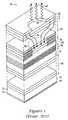
- FIG. 1illustrates a typical VCSEL 10 .
- an n-doped gallium arsenide (GaAS) substrate 12has an n-type electrical contact 14 .
- An n-doped lower mirror stack 16(a DBR) is on the GaAS substrate 12 , and an n-type graded-index lower spacer 18 is disposed over the lower mirror stack 16 .
- An active region 20is formed over the lower spacer 18 .
- a p-type graded-index top spacer 22is disposed over the active region 20 , and a p-type top mirror stack 24 (another DBR) is disposed over the top spacer 22 .
- Over the top mirror stack 24is a p-type conduction layer 9 , a p-type GaAs cap layer 8 , and a p-type electrical contact 26 .
- the lower spacer 18 and the top spacer 22separate the lower mirror stack 16 from the top mirror stack 24 such that an optical cavity is formed.
- the mirror separationis controlled to resonant at a predetermined wavelength (or at a multiple thereof).
- At least part of the top mirror stack 24includes an insulating region 40 that provides for current confinement.
- the insulating region 40is usually formed either by implanting protons into the top mirror stack 24 or by forming an oxide layer.
- the insulating region 40defines a conductive annular central opening 42 that forms an electrically conductive path though the insulating region 40 .
- an external biascauses an electrical current 21 to flow from the p-type electrical contact 26 toward the n-type electrical contact 14 .
- the insulating region 40 and the conductive central opening 42confine the current 21 such that it flows through the conductive central opening 42 to the active region 20 .
- Some of the electrons in the current 21are converted into photons in the active region 20 .
- Those photonsbounce back and forth (resonate) between the lower mirror stack 16 and the top mirror stack 24 .
- the lower mirror stack 16 and the top mirror stack 24are very good reflectors, some of the photons leak out as light 23 that travels along an optical path. Still referring to FIG. 1, the light 23 passes through the p-type conduction layer 9 , through the p-type GaAs cap layer 8 , through an aperture 30 in the p-type electrical contact 26 , and out of the surface of the vertical cavity surface emitting laser 10 .
- FIG. 1illustrates a typical VCSEL, and that numerous variations are possible.
- the dopingscan be changed (say, by providing a p-type substrate 12 ), different material systems can be used, operational details can be tuned for maximum performance, and additional structures, such as tunnel junctions, can be added.
- DBRdistributed Bragg Reflector
- a DBRIn many applications a DBR must be both highly reflective and highly electrically conductive. In fact, when used in a VCSEL a DBR must be particularly reflective so as to reduce optical losses to such a degree that laser operation is enabled. Reflectivity is achieved by stacking material layers having significantly different indexes of refraction, for example, by stacking alternating layers of AlAs and GaAs. Such stacked layers can produce an optical standing wave within the DBR.
- top DBRswhich are usually p-doped.
- the lower mobility of the p-carriers and the higher optical absorption of p-dopantstend to reduce the performance of such top DBRs. Therefore, a conflict occurs in prior art long wavelength VCSELs: to reduce electrical resistance the free carrier concentration should be high, but to reduce light absorption the free carrier concentration should be low.
- DBRsproduce optical standing waves that are characterized by spatially dependent electrical fields. That is, the electric field strength varies across the DBR's thickness.
- the materials that form a DBRstrongly impact on the thermal characteristics of a VCSEL.
- Binary phase materials, such as AlAs and GaAstend to have very good thermal conductivity. Thus, heat flows across AlAs and GaAs stacks very well.
- the transition regionwhich is characterized by three materials, has a significantly lower thermal conductivity. This is because the crystalline structure of the transition region is highly distorted, which reduces thermal conductivity.
- DBRs used in prior art VCSELshave problems with excessive optical absorption, relatively poor thermal conductivity, and relatively high electrical resistance, particularly when producing long wavelength light. Therefore, a new distributed Bragg reflector that has relatively low light absorption and relatively low electrical resistance, particularly at long wavelengths and in top DBRs, would be beneficial. Even more beneficial would be a new distributed Bragg reflector that has relatively low light absorption, relatively low electrical resistance, and relatively good thermal conductivity, particularly at long wavelengths and in top DBRs.
- the principles of the present inventionare directed to a new distributed Bragg reflector (DBR) having low light absorption and low electrical resistance.
- DBRdistributed Bragg reflector
- such a DBRis implemented in a manner that results in good thermal conductivity.
- a distributed Bragg reflectoris comprised of stacked material layers having different indexes of refraction that are joined by asymmetrical transition regions in which the transition steps within a transition region have different material compositions, different doping levels, and different layer thicknesses. Furthermore, the adjacent transition regions having transition steps with different thicknesses and different doping levels. Beneficially, adjacent transition regions have different overall thicknesses, with the thinner transition regions being relatively highly doped and located where the optical standing wave within the DBR has low field strength, and with the thicker transition regions being relatively lightly doped and located where the optical standing wave has a relatively high field strength. The thinner transition regions improve both electrical and thermal conductivity.
- the stacked material layersare comprised of alternating layers of ALAs and GaAs. Even more beneficially, the stacked material layers form a p-doped top mirror of a VCSEL, such as a long wavelength VCSEL.
- FIG. 1illustrates a typical vertical cavity surface emitting laser
- FIG. 2illustrates a vertical cavity surface emitting laser according to the principles of the present invention
- FIG. 3illustrates a distributed Bragg reflector having a standing optical wave, with that distributed Bragg reflector being in accord with the principles of the present invention.
- the principles of the present inventionprovide for asymmetrical distributed Bragg reflectors (DBRs), and for VCSELs that use asymmetrical DBRs.
- DBRsdistributed Bragg reflectors
- VCSELsVCSELs that use asymmetrical DBRs.
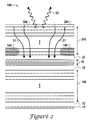
- FIG. 2for an illustration of a vertical cavity surface emitting laser (VCSEL) 100 that is in accord with the principles of the present invention.
- FIG. 2should be understood as a simplified “cut-away” schematic depiction of a VCSEL that is generally configured as shown in FIG. 1. Thus, similar element numbers will be used for similar elements in FIG. 2 as were used in FIG. 1.
- the VCSEL 100includes novel and useful top and bottom distributed Bragg reflectors (DBRs).
- DBRsdistributed Bragg reflectors
- the VCSEL 100includes an n-doped gallium arsenide (GaAS) substrate 12 having an n-type electrical contact 14 .
- An n-doped lower mirror stack 160(a DBR) is on the GaAS substrate 12 , and an n-type graded-index lower spacer 18 is disposed over the lower mirror stack 160 .
- the lower mirror stack 160is described in more detail subsequently.
- An active region 20 having P-N junction structures with a number of quantum wellsis formed over the lower spacer 18 .
- the composition of the active region 20is beneficially AlGaAs, with the specific aluminum content varying in the different layers that form the active region 20 .
- one layermay have between twenty and thirty percent of aluminum, while an adjacent layer might have between zero and five percent of aluminum. There could be many alternating layers, depending how the quantum wells are to be in the active region 20 .
- a p-type graded-index top spacer 22On the active region 20 is a p-type graded-index top spacer 22 .
- a p-type top mirror stack 240(another DBR) is disposed over the top spacer 22 .
- the upper mirror stack 240is described in more detail subsequently.
- top mirror stack 240Over the top mirror stack 240 is a p-type conduction layer, a p-type GaAs cap layer, and a p-type electrical contact, all of which are designated as 260 .
- the lower spacer 18 and the top spacer 22separate the lower mirror stack 160 from the top mirror stack 240 such that an optical cavity that is resonant at a specific wavelength is formed.
- the top mirror stack 240includes an insulating region 140 , which is beneficially produced by forming the top mirror stack 240 with an AlGaAs layer(s) having a high aluminum content (97-98%), and then oxidizing that high aluminum content layer along an annular ring. Oxidation then produces the oxide insulating region 140 .
- an external biascauses an electrical current 21 to flow into the VCSEL 100 .
- the insulating region 140forms a current guide into the active region 20 where some of the electrons are converted into photons. Those photons bounce back and forth (resonate) between the lower mirror stack 160 and the top mirror stack 240 . While the lower mirror stack 160 and the top mirror stack 240 are very good reflectors, some of the photons leak out as light 23 that travels along an optical path. Still referring to FIG. 2, the light 23 passes through an opening 300 in the element 260 and out of the surface of the vertical cavity surface emitting laser 100 .
- the VCSEL 100 of FIG. 2significantly differs from the VCSEL 10 of FIG. 1 by asymmetry in the top mirror stack 240 and in the lower minor stack 160 .
- Those mirror stacksare beneficially formed from layers of different compositions of Al x Ga 1-x As. While the principles of the present invention are particularly suitable for use in p-doped top mirror stacks (because p-doped materials are optically more absorbent, those materials benefit more from the present invention), those principles are suitable for use with either type of doping.
- the illustrated embodimentis based on the AlxGa 1 -xAs material system, the principles of the present invention are applicable to a wide range of compound semiconductor material systems.
- FIG. 3illustrates a distributed Bragg reflector 400 that is suitable for use as either (or both) the lower mirror stack 160 or the top mirror stack 240 .
- a standing waveis developed within the Distributed Bragg Reflector.
- a normalized power waveform 402 of such a standing waveis superimposed on the distributed Bragg reflector 400 .
- FIG. 3also illustrates relative thicknesses of the individual layers that comprise the distributed Bragg reflector 400 , with the relative thickness of each layer being indicated by the space between vertical lines.
- the distributed Bragg reflector 400includes at least layers 280 through 320 . In practice there can be multiple sets of such layers (thus a given distributed Bragg reflector could be comprised of hundreds of individual layers).
- the closest vertical line spacingoccurs where the electric field is smallest (close to zero), say around layer 300 .
- the layers that form that junctionhave relatively high doping levels, which decrease the electrical resistance across the AlAs-to-GaAs transition region.
- the electric fieldis low in that transition region, the optical absorption is also low, despite the high doping levels.
- the vertical line spacingis the relatively large, which represents relatively thick individual layers. This represents an interface junction where the GaAs (0% Al) composition changes to AlAs (0% Ga). That area is relatively lightly doped to help to decrease optical absorption of the locally high electric field.
- the relatively large thickness of the GaAs-to-AlAs transition regionhelps to decrease the electrical resistance without significantly increasing the optical absorption.
- a DBR that is in accord with the principles of the present inventionis asymmetric in both the interface junction thickness and in the interface junction doping profile.
- the use of a coupled doping profile and composition profilealso contributes to the improved performance of this invention.
- An embodiment of an asymmetric p-doped DBR for use at 1310 nm in the Al x Ga 1-x As material system having a 0% to 100% Al composition rangeis provided for in Table 1. Specific layer thicknesses, doping concentrations, and material compositions are provided.
- the first interface junction in Table 1is the AlAs (100% Al composition) to GaAs (0% Al composition) heterojunction, consisting of the layers in row 1 through row 10.
- the layers of the second interface junction, the GaAs (0% Al composition) to AlAs (100% Al composition) heterojunctionare listed in row 13 through row 22.
- the asymmetry of this embodimentcan be seen by comparing the total thickness of the first interface junction, 20 nm, with that of the second interface junction, 40 nm. This asymmetry is also seen as the steeper average slope of the leftmost, downward transition in material composition in FIG. 4 as compared with the less steep average slope of the rightmost, upward transition. Note that the doping concentration of the first interface junction ranges from 2.86E+18 cm ⁇ 3 to 6.17E+18 cm ⁇ 3, while that of the second interface junction ranges from 6.65E+17 cm ⁇ 3 to 1.93E+18 cm ⁇ 3.
- the asymmetry in the interface junction thickness and the asymmetry in doping rangework together to provide a lower optical absorption and lower electrical resistance than either separately.
- Table 2provides another embodiment DBR that is in accord with the principles of the present invention. That DBR is a p-doped Al x Ga (1-x) As DBR suitable for use in a 1310 nm VCSEL. That DBR has a restricted Al composition range of 0% to 85%.
Landscapes
- Physics & Mathematics (AREA)
- Condensed Matter Physics & Semiconductors (AREA)
- General Physics & Mathematics (AREA)
- Electromagnetism (AREA)
- Optics & Photonics (AREA)
- Semiconductor Lasers (AREA)
- Lasers (AREA)
Abstract
Description
- Not applicable.[0001]
- 1. Field of the Invention[0002]
- The present invention relates to laser mirror structures. More specifically, it relates to mirror structures suitable for use in vertical cavity surface emitting lasers.[0003]
- 2. Discussion of the Related Art[0004]
- Vertical cavity surface emitting lasers (VCSELs) represent a relatively new class of semiconductor lasers. While there are many variations of VCSELs, one common characteristic is that they emit light perpendicular to a wafer's surface. Advantageously, VCSELs can be formed from a wide range of material systems to produce specific characteristics. In particular, the various material systems can be tailored to produce different laser wavelengths, such as 1550 nm, 1310 nm, 850 nm, 670 nm, and so on.[0005]
- VCSELs include semiconductor active regions, distributed Bragg reflector (DBR) mirrors, current confinement structures, substrates, and contacts. Because of their complicated structure, and because of their material requirements, VCSELs are usually grown using metal-organic chemical vapor deposition (MOCVD) or molecular beam epitaxy (MBE).[0006]
- FIG. 1 illustrates a[0007]
typical VCSEL 10. As shown, an n-doped gallium arsenide (GaAS)substrate 12 has an n-typeelectrical contact 14. An n-doped lower mirror stack16 (a DBR) is on the GaASsubstrate 12, and an n-type graded-indexlower spacer 18 is disposed over thelower mirror stack 16. Anactive region 20, usually having a number of quantum wells, is formed over thelower spacer 18. A p-type graded-indextop spacer 22 is disposed over theactive region 20, and a p-type top mirror stack24 (another DBR) is disposed over thetop spacer 22. Over thetop mirror stack 24 is a p-type conduction layer 9, a p-typeGaAs cap layer 8, and a p-typeelectrical contact 26. - Still referring to FIG. 1, the[0008]
lower spacer 18 and thetop spacer 22 separate thelower mirror stack 16 from thetop mirror stack 24 such that an optical cavity is formed. As the optical cavity is resonant at specific wavelengths, the mirror separation is controlled to resonant at a predetermined wavelength (or at a multiple thereof). At least part of thetop mirror stack 24 includes aninsulating region 40 that provides for current confinement. Theinsulating region 40 is usually formed either by implanting protons into thetop mirror stack 24 or by forming an oxide layer. Theinsulating region 40 defines a conductive annularcentral opening 42 that forms an electrically conductive path though theinsulating region 40. - In operation, an external bias causes an[0009]
electrical current 21 to flow from the p-typeelectrical contact 26 toward the n-typeelectrical contact 14. Theinsulating region 40 and the conductivecentral opening 42 confine the current21 such that it flows through the conductivecentral opening 42 to theactive region 20. Some of the electrons in the current21 are converted into photons in theactive region 20. Those photons bounce back and forth (resonate) between thelower mirror stack 16 and thetop mirror stack 24. While thelower mirror stack 16 and thetop mirror stack 24 are very good reflectors, some of the photons leak out aslight 23 that travels along an optical path. Still referring to FIG. 1, thelight 23 passes through the p-type conduction layer 9, through the p-typeGaAs cap layer 8, through anaperture 30 in the p-typeelectrical contact 26, and out of the surface of the vertical cavitysurface emitting laser 10. - It should be understood that FIG. 1 illustrates a typical VCSEL, and that numerous variations are possible. For example, the dopings can be changed (say, by providing a p-type substrate[0010]12), different material systems can be used, operational details can be tuned for maximum performance, and additional structures, such as tunnel junctions, can be added.
- While generally successful, VCSELs have problems. In particular, in some applications the available prior art distributed Bragg Reflectors (DBR) are significantly less than optimal. To understand why this is so it is beneficial to consider DBRs in more detail.[0011]
- In many applications a DBR must be both highly reflective and highly electrically conductive. In fact, when used in a VCSEL a DBR must be particularly reflective so as to reduce optical losses to such a degree that laser operation is enabled. Reflectivity is achieved by stacking material layers having significantly different indexes of refraction, for example, by stacking alternating layers of AlAs and GaAs. Such stacked layers can produce an optical standing wave within the DBR.[0012]
- While the optical performance of stacked AlAs and GaAs is very good, an abrupt junction between an AlAs layer and a GaAs layer would form a high barrier to current flow. To reduce that barrier, the layers of AlAs and GaAs are joined using a transition region in which the material composition gradually changes from AlAs to GaAs. Furthermore, in most VCSELs the DBR layers are doped to provide free carriers that reduce electrical resistance. The result is a structure that, ideally, has high reflectivity combined with both low optical absorption and low electrical resistance.[0013]
- In practice, optical absorption increases with increasing electric field strength, increasing wavelength, and increasing doping levels. Furthermore, p-type dopants tend to have higher optical absorption than n-type dopants. On the other hand, electrical resistance is relatively unaffected by electrical field strength and optical wavelength, yet decreases with increasing doping levels. But, p-type carriers (holes) have much lower mobilities than n-type carriers (electrons). Therefore, as the wavelength increases, such as with VCSELs that output light at 1300, 1310, or 1550 nm, obtaining both low optical absorption and low electrical resistance is difficult. This is because long optical wavelengths tend to be highly absorbed by the free carriers that reduce the electrical resistance. Such is particularly true in top DBRs, which are usually p-doped. The lower mobility of the p-carriers and the higher optical absorption of p-dopants tend to reduce the performance of such top DBRs. Therefore, a conflict occurs in prior art long wavelength VCSELs: to reduce electrical resistance the free carrier concentration should be high, but to reduce light absorption the free carrier concentration should be low.[0014]
- In addition, it should be understood that DBRs produce optical standing waves that are characterized by spatially dependent electrical fields. That is, the electric field strength varies across the DBR's thickness. Additionally, the materials that form a DBR strongly impact on the thermal characteristics of a VCSEL. Binary phase materials, such as AlAs and GaAs tend to have very good thermal conductivity. Thus, heat flows across AlAs and GaAs stacks very well. However, the transition region, which is characterized by three materials, has a significantly lower thermal conductivity. This is because the crystalline structure of the transition region is highly distorted, which reduces thermal conductivity.[0015]
- Because of the foregoing, DBRs used in prior art VCSELs have problems with excessive optical absorption, relatively poor thermal conductivity, and relatively high electrical resistance, particularly when producing long wavelength light. Therefore, a new distributed Bragg reflector that has relatively low light absorption and relatively low electrical resistance, particularly at long wavelengths and in top DBRs, would be beneficial. Even more beneficial would be a new distributed Bragg reflector that has relatively low light absorption, relatively low electrical resistance, and relatively good thermal conductivity, particularly at long wavelengths and in top DBRs.[0016]
- The following summary of the invention is provided to facilitate an understanding of some of the innovative features unique to the present invention, and is not intended to be a full description. A full appreciation of the various aspects of the invention can be gained by taking the entire specification, claims, drawings, and abstract as a whole.[0017]
- Accordingly, the principles of the present invention are directed to a new distributed Bragg reflector (DBR) having low light absorption and low electrical resistance. Beneficially, such a DBR is implemented in a manner that results in good thermal conductivity.[0018]
- A distributed Bragg reflector according to the principles of the present invention is comprised of stacked material layers having different indexes of refraction that are joined by asymmetrical transition regions in which the transition steps within a transition region have different material compositions, different doping levels, and different layer thicknesses. Furthermore, the adjacent transition regions having transition steps with different thicknesses and different doping levels. Beneficially, adjacent transition regions have different overall thicknesses, with the thinner transition regions being relatively highly doped and located where the optical standing wave within the DBR has low field strength, and with the thicker transition regions being relatively lightly doped and located where the optical standing wave has a relatively high field strength. The thinner transition regions improve both electrical and thermal conductivity.[0019]
- Beneficially, the stacked material layers are comprised of alternating layers of ALAs and GaAs. Even more beneficially, the stacked material layers form a p-doped top mirror of a VCSEL, such as a long wavelength VCSEL.[0020]
- The novel features of the present invention will become apparent to those of skill in the art upon examination of the following detailed description of the invention or can be learned by practice of the present invention. It should be understood, however, that the detailed description of the invention and the specific examples presented, while indicating certain embodiments of the present invention, are provided for illustration purposes only because various changes and modifications within the spirit and scope of the invention will become apparent to those of skill in the art from the detailed description of the invention and claims that follow.[0021]
- The accompanying figures, in which like reference numerals refer to identical or functionally-similar elements throughout the separate views and which are incorporated in and form part of the specification, further illustrate the present invention and, together with the detailed description of the invention, serve to explain the principles of the present invention.[0022]
- In the drawings:[0023]
- FIG. 1 illustrates a typical vertical cavity surface emitting laser;[0024]
- FIG. 2 illustrates a vertical cavity surface emitting laser according to the principles of the present invention; and[0025]
- FIG. 3 illustrates a distributed Bragg reflector having a standing optical wave, with that distributed Bragg reflector being in accord with the principles of the present invention.[0026]
- Note that in the drawings that like numbers designate like elements. Additionally, for explanatory convenience the descriptions use directional signals such as up and down, top and bottom, and lower and upper. Such signals, which are derived from the relative positions of the elements illustrated in the drawings, are meant to aid the understanding of the present invention, not to limit it.[0027]
- Reference will now be made in detail to an embodiment of the present invention, example of which is illustrated in the accompanying drawings.[0028]
- The principles of the present invention provide for asymmetrical distributed Bragg reflectors (DBRs), and for VCSELs that use asymmetrical DBRs.[0029]
- Refer now to FIG. 2 for an illustration of a vertical cavity surface emitting laser (VCSEL)[0030]100 that is in accord with the principles of the present invention. FIG. 2 should be understood as a simplified “cut-away” schematic depiction of a VCSEL that is generally configured as shown in FIG. 1. Thus, similar element numbers will be used for similar elements in FIG. 2 as were used in FIG. 1. However, the
VCSEL 100 includes novel and useful top and bottom distributed Bragg reflectors (DBRs). - As shown in FIG. 2, the[0031]
VCSEL 100 includes an n-doped gallium arsenide (GaAS)substrate 12 having an n-typeelectrical contact 14. An n-doped lower mirror stack160 (a DBR) is on theGaAS substrate 12, and an n-type graded-indexlower spacer 18 is disposed over thelower mirror stack 160. Thelower mirror stack 160 is described in more detail subsequently. - An[0032]
active region 20 having P-N junction structures with a number of quantum wells is formed over thelower spacer 18. The composition of theactive region 20 is beneficially AlGaAs, with the specific aluminum content varying in the different layers that form theactive region 20. For example, one layer may have between twenty and thirty percent of aluminum, while an adjacent layer might have between zero and five percent of aluminum. There could be many alternating layers, depending how the quantum wells are to be in theactive region 20. - On the[0033]
active region 20 is a p-type graded-index top spacer 22. A p-type top mirror stack240 (another DBR) is disposed over thetop spacer 22. Theupper mirror stack 240 is described in more detail subsequently. - Over the[0034]
top mirror stack 240 is a p-type conduction layer, a p-type GaAs cap layer, and a p-type electrical contact, all of which are designated as260. As in the VCSEL10 (see FIG. 1), thelower spacer 18 and thetop spacer 22 separate thelower mirror stack 160 from thetop mirror stack 240 such that an optical cavity that is resonant at a specific wavelength is formed. - Still referring to FIG. 2, the[0035]
top mirror stack 240 includes aninsulating region 140, which is beneficially produced by forming thetop mirror stack 240 with an AlGaAs layer(s) having a high aluminum content (97-98%), and then oxidizing that high aluminum content layer along an annular ring. Oxidation then produces theoxide insulating region 140. - In operation, an external bias causes an electrical current[0036]21 to flow into the
VCSEL 100. Theinsulating region 140 forms a current guide into theactive region 20 where some of the electrons are converted into photons. Those photons bounce back and forth (resonate) between thelower mirror stack 160 and thetop mirror stack 240. While thelower mirror stack 160 and thetop mirror stack 240 are very good reflectors, some of the photons leak out as light23 that travels along an optical path. Still referring to FIG. 2, the light23 passes through anopening 300 in theelement 260 and out of the surface of the vertical cavitysurface emitting laser 100. - The[0037]
VCSEL 100 of FIG. 2 significantly differs from theVCSEL 10 of FIG. 1 by asymmetry in thetop mirror stack 240 and in the lowerminor stack 160. Those mirror stacks are beneficially formed from layers of different compositions of AlxGa1-xAs. While the principles of the present invention are particularly suitable for use in p-doped top mirror stacks (because p-doped materials are optically more absorbent, those materials benefit more from the present invention), those principles are suitable for use with either type of doping. Furthermore, while the illustrated embodiment is based on the AlxGa1-xAs material system, the principles of the present invention are applicable to a wide range of compound semiconductor material systems. - FIG. 3 illustrates a distributed[0038]
Bragg reflector 400 that is suitable for use as either (or both) thelower mirror stack 160 or thetop mirror stack 240. In operation, a standing wave is developed within the Distributed Bragg Reflector. A normalizedpower waveform 402 of such a standing wave, as computed by an optical simulation of a particular embodiment of this invention, is superimposed on the distributedBragg reflector 400. FIG. 3 also illustrates relative thicknesses of the individual layers that comprise the distributedBragg reflector 400, with the relative thickness of each layer being indicated by the space between vertical lines. As shown in FIG. 3, the distributedBragg reflector 400 includes atleast layers 280 through320. In practice there can be multiple sets of such layers (thus a given distributed Bragg reflector could be comprised of hundreds of individual layers). - Still referring to FIG. 3, the closest vertical line spacing occurs where the electric field is smallest (close to zero), say around[0039]
layer 300. This indicates the relatively small thicknesses of the layers that form an AlAs-to-GaAs junction (where the composition changes from 100% AlAs to 100% GaAs). The layers that form that junction have relatively high doping levels, which decrease the electrical resistance across the AlAs-to-GaAs transition region. However, because the electric field is low in that transition region, the optical absorption is also low, despite the high doping levels. - However, still referring to FIG. 3, where the electric field is high (say around layer[0040]290) the vertical line spacing is the relatively large, which represents relatively thick individual layers. This represents an interface junction where the GaAs (0% Al) composition changes to AlAs (0% Ga). That area is relatively lightly doped to help to decrease optical absorption of the locally high electric field. The relatively large thickness of the GaAs-to-AlAs transition region helps to decrease the electrical resistance without significantly increasing the optical absorption.
- Thus, a DBR that is in accord with the principles of the present invention is asymmetric in both the interface junction thickness and in the interface junction doping profile. The use of a coupled doping profile and composition profile also contributes to the improved performance of this invention.[0041]
- An embodiment of an asymmetric p-doped DBR for use at 1310 nm in the Al[0042]xGa1-xAs material system having a 0% to 100% Al composition range is provided for in Table 1. Specific layer thicknesses, doping concentrations, and material compositions are provided. The first interface junction in Table 1 is the AlAs (100% Al composition) to GaAs (0% Al composition) heterojunction, consisting of the layers in row 1 through
row 10. Similarly, the layers of the second interface junction, the GaAs (0% Al composition) to AlAs (100% Al composition) heterojunction, are listed in row 13 throughrow 22. - The asymmetry of this embodiment can be seen by comparing the total thickness of the first interface junction, 20 nm, with that of the second interface junction, 40 nm. This asymmetry is also seen as the steeper average slope of the leftmost, downward transition in material composition in FIG. 4 as compared with the less steep average slope of the rightmost, upward transition. Note that the doping concentration of the first interface junction ranges from 2.86E+18 cm−3 to 6.17E+18 cm−3, while that of the second interface junction ranges from 6.65E+17 cm−3 to 1.93E+18 cm−3. The asymmetry in the interface junction thickness and the asymmetry in doping range work together to provide a lower optical absorption and lower electrical resistance than either separately.[0043]
TABLE 1 Thickness Dopant Composition Layer (nm) Concentration (cm−3) (% Al) 1 2.50 6.17E+18 99 2 2.50 6.42E+18 94 3 2.00 6.22E+18 84 4 1.50 5.59E+18 71 5 1.50 4.79E+18 52 6 1.50 4.22E+18 42 7 1.50 3.44E+18 29 8 2.00 2.88E+18 15 9 2.50 2.61E+18 5 10 2.50 2.86E+18 1 11 33.99 2.86E+18 0 12 33.99 6.65E+17 0 13 5.00 6.65E+17 1 14 5.00 3.42E+17 5 15 4.00 3.80E+17 15 16 3.00 6.94E+17 0.29 17 3.00 1.11E+18 0.42 18 3.00 1.37E+18 52 19 3.00 1.90E+18 71 20 4.00 2.23E+18 84 21 5.00 2.28 + 18 94 22 5.00 1.93 + 18 99 23 36.71 1.93 + 18 100 24 36.71 6.17 + 18 100 - There are circumstances for which a 0% to 100% range in material composition variation is undesirable. Therefore, Table 2 provides another embodiment DBR that is in accord with the principles of the present invention. That DBR is a p-doped Al[0044]xGa(1-x)As DBR suitable for use in a 1310 nm VCSEL. That DBR has a restricted Al composition range of 0% to 85%.
TABLE 2 Thickness Dopant Composition Layer (nm) Concentration (cm−3) (% A1) 1 2.50 4.77E+18 84 2 2.50 4.96E+18 80 3 2.00 4.80E+18 71 4 1.50 4.32E+18 60 5 1.50 3.70E+18 44 6 1.50 3.26E+18 36 7 1.50 2.66E+18 25 8 2.00 2.23E+18 13 9 2.50 2.01E+18 4 10 2.50 2.21E+18 1 11 33.99 2.21E+18 0 12 33.99 7.00E+17 0 13 5.00 7.00E+17 1 14 5.00 3.60E+17 4 15 4.00 4.00E+17 13 16 3.00 7.30E+17 25 17 3.00 1.17E+18 36 18 3.00 1.44E+18 44 19 3.00 2.00E+18 60 20 4.00 2.35E+18 71 21 5.00 2.40E+18 80 22 5.00 2.03E+18 84 23 36.71 2.03E+18 85 24 36.71 4.77E+18 85 - The two-fold asymmetry of total interface junction thickness and doping concentration range of this embodiment is apparent from Table 2. Furthermore, comparing the rows of Table 2 with the corresponding rows of Table 1 shows that the doping concentration ranges differ in addition to the material composition ranges. Thus, the best embodiments of this invention may vary in many ways, including the number of steps, the individual step size, the total heterojunction thickness, the doping concentration range and the material composition range.[0045]
- The embodiments and examples set forth herein are presented to best explain the present invention and its practical application and to thereby enable those skilled in the art to make and utilize the invention. Those skilled in the art, however, will recognize that the foregoing description and examples have been presented for the purpose of illustration and example only. Other variations and modifications of the present invention will be apparent to those of skill in the art, and it is the intent of the appended claims that such variations and modifications be covered. The description as set forth is not intended to be exhaustive or to limit the scope of the invention. Many modifications and variations are possible in light of the above teaching without departing from the spirit and scope of the following claims. It is contemplated that the use of the present invention can involve components having different characteristics. It is intended that the scope of the present invention be defined by the claims appended hereto, giving full cognizance to equivalents in all respects.[0046]
Claims (26)
Priority Applications (9)
| Application Number | Priority Date | Filing Date | Title |
|---|---|---|---|
| US10/028,435US6850548B2 (en) | 2001-12-28 | 2001-12-28 | Assymmetric distributed Bragg reflector for vertical cavity surface emitting lasers |
| CNA028261887ACN1613170A (en) | 2001-12-28 | 2002-12-13 | Asymmetric distributed Bragg reflector for vertical cavity surface emitting lasers |
| KR1020047010027AKR100558320B1 (en) | 2001-12-28 | 2002-12-13 | Asymmetric Distribution Bragg Reflector for Vertical Resonant Surface Emitting Laser |
| DE60238275TDE60238275D1 (en) | 2001-12-28 | 2002-12-13 | ASYMMETRICALLY DISTRIBUTED BRAGG REFLECTOR FOR SURFACE EMITTING LASER WITH VERTICAL RESONATOR |
| AT02798511TATE488039T1 (en) | 2001-12-28 | 2002-12-13 | ASYMMETRICALLY DISTRIBUTED BRAGG REFLECTOR FOR SURFACE EMITTING LASER WITH VERTICAL RESONATOR |
| JP2003558979AJP4177262B2 (en) | 2001-12-28 | 2002-12-13 | Asymmetric distributed Bragg reflector for vertical cavity surface emitting lasers |
| EP02798511AEP1459417B1 (en) | 2001-12-28 | 2002-12-13 | Asymmetric distributed bragg reflector for vertical cavity surface emitting lasers |
| PCT/US2002/039825WO2003058774A2 (en) | 2001-12-28 | 2002-12-13 | Asymmetric distributed bragg reflector for vertical cavity surface emitting lasers |
| TW091137479ATWI237935B (en) | 2001-12-28 | 2002-12-26 | Asymmetric distributed bragg reflector for vertical cavity surface emitting lasers |
Applications Claiming Priority (1)
| Application Number | Priority Date | Filing Date | Title |
|---|---|---|---|
| US10/028,435US6850548B2 (en) | 2001-12-28 | 2001-12-28 | Assymmetric distributed Bragg reflector for vertical cavity surface emitting lasers |
Publications (2)
| Publication Number | Publication Date |
|---|---|
| US20030123513A1true US20030123513A1 (en) | 2003-07-03 |
| US6850548B2 US6850548B2 (en) | 2005-02-01 |
Family
ID=21843427
Family Applications (1)
| Application Number | Title | Priority Date | Filing Date |
|---|---|---|---|
| US10/028,435Expired - LifetimeUS6850548B2 (en) | 2001-12-28 | 2001-12-28 | Assymmetric distributed Bragg reflector for vertical cavity surface emitting lasers |
Country Status (9)
| Country | Link |
|---|---|
| US (1) | US6850548B2 (en) |
| EP (1) | EP1459417B1 (en) |
| JP (1) | JP4177262B2 (en) |
| KR (1) | KR100558320B1 (en) |
| CN (1) | CN1613170A (en) |
| AT (1) | ATE488039T1 (en) |
| DE (1) | DE60238275D1 (en) |
| TW (1) | TWI237935B (en) |
| WO (1) | WO2003058774A2 (en) |
Cited By (12)
| Publication number | Priority date | Publication date | Assignee | Title |
|---|---|---|---|---|
| US20040208216A1 (en)* | 2001-04-11 | 2004-10-21 | Naone Ryan Likeke | Long wavelength vertical cavity surface emitting laser |
| US20060045162A1 (en)* | 2004-08-31 | 2006-03-02 | Finisar Corporation | Distributed bragg reflector for optoelectronic device |
| US20060072639A1 (en)* | 2004-10-01 | 2006-04-06 | Johnson Ralph H | Vertical cavity surface emitting laser with undoped top mirror |
| US20060268954A1 (en)* | 2004-08-31 | 2006-11-30 | Johnson Ralph H | Light emitting semiconductor device having an electrical confinement barrier near the active region |
| US20070127536A1 (en)* | 2004-10-01 | 2007-06-07 | Finisar Corporation | Semiconductor having enhanced carbon doping |
| US20070254393A1 (en)* | 2004-10-01 | 2007-11-01 | Finisar Corporation | Passivation of vcsel sidewalls |
| US7826506B2 (en) | 2004-10-01 | 2010-11-02 | Finisar Corporation | Vertical cavity surface emitting laser having multiple top-side contacts |
| US7829912B2 (en) | 2006-07-31 | 2010-11-09 | Finisar Corporation | Efficient carrier injection in a semiconductor device |
| US20110096803A1 (en)* | 2007-12-21 | 2011-04-28 | Finisar Corporation | Asymmetric dbr pairs combined with periodic and modulation doping to maximize conduction and reflectivity, and minimize absorption |
| US8031752B1 (en) | 2007-04-16 | 2011-10-04 | Finisar Corporation | VCSEL optimized for high speed data |
| EP3509171A3 (en)* | 2018-01-09 | 2019-07-24 | Lg Innotek Co. Ltd | Surface-emitting laser device and light emitting device including the same |
| US12027819B2 (en) | 2018-03-15 | 2024-07-02 | Trumpf Photonic Components Gmbh | Vertical cavity surface emitting laser device with integrated tunnel junction |
Families Citing this family (10)
| Publication number | Priority date | Publication date | Assignee | Title |
|---|---|---|---|---|
| US7245647B2 (en)* | 1999-10-28 | 2007-07-17 | Ricoh Company, Ltd. | Surface-emission laser diode operable in the wavelength band of 1.1-1.7mum and optical telecommunication system using such a laser diode |
| US6975663B2 (en)* | 2001-02-26 | 2005-12-13 | Ricoh Company, Ltd. | Surface-emission laser diode operable in the wavelength band of 1.1-7μm and optical telecommunication system using such a laser diode |
| US7590159B2 (en)* | 2001-02-26 | 2009-09-15 | Ricoh Company, Ltd. | Surface-emission laser diode operable in the wavelength band of 1.1-1.7 micrometers and optical telecommunication system using such a laser diode |
| KR100737609B1 (en)* | 2005-09-29 | 2007-07-10 | 엘지전자 주식회사 | Vertical external resonant surface emitting light pumping semiconductor laser and its manufacturing method |
| JP4300245B2 (en)* | 2006-08-25 | 2009-07-22 | キヤノン株式会社 | Optical element equipped with multilayer reflector, surface emitting laser |
| US8527939B2 (en)* | 2006-09-14 | 2013-09-03 | Sap Ag | GUI modeling of knowledge base in a modeling environment |
| CN102611000B (en)* | 2012-03-23 | 2013-09-25 | 中国科学院长春光学精密机械与物理研究所 | High-efficiency vertical cavity surface emitting semiconductor laser with asymmetric optical field distribution |
| WO2018031582A1 (en) | 2016-08-08 | 2018-02-15 | Finisar Corporation | Etched planarized vcsel |
| CN111630735B (en)* | 2018-01-18 | 2024-07-26 | Iqe公司 | Porous distributed Bragg reflector for laser applications |
| CN116207612A (en)* | 2023-03-30 | 2023-06-02 | 扬州乾照光电有限公司 | A kind of VCSEL epitaxy structure and manufacturing method thereof, VCSEL chip |
Citations (8)
| Publication number | Priority date | Publication date | Assignee | Title |
|---|---|---|---|---|
| US5745515A (en)* | 1996-07-18 | 1998-04-28 | Honeywell Inc. | Self-limiting intrinsically eye-safe laser utilizing an increasing absorption layer |
| US5764671A (en)* | 1996-10-21 | 1998-06-09 | Motorola, Inc. | VCSEL with selective oxide transition regions |
| US5848086A (en)* | 1996-12-09 | 1998-12-08 | Motorola, Inc. | Electrically confined VCSEL |
| US6201825B1 (en)* | 1998-05-29 | 2001-03-13 | Fuji Xerox Co., Ltd. | Surface emitting semiconductor laser device and process for producing the same |
| US20020131461A1 (en)* | 2001-03-15 | 2002-09-19 | Honeywell International Inc., | Vertical cavity master oscillator power amplifier |
| US20020150135A1 (en)* | 2001-04-11 | 2002-10-17 | Naone Ryan Likeke | Long wavelength vertical cavity surface emitting laser |
| US20030031221A1 (en)* | 2000-04-05 | 2003-02-13 | Coretek, Inc. | Single mode operation of microelectromechanically tunable, half-symmetric, vertical cavity surface emitting lasers |
| US6611543B2 (en)* | 2000-12-23 | 2003-08-26 | Applied Optoelectronics, Inc. | Vertical-cavity surface-emitting laser with metal mirror and method of fabrication of same |
Family Cites Families (2)
| Publication number | Priority date | Publication date | Assignee | Title |
|---|---|---|---|---|
| US5170407A (en) | 1991-10-11 | 1992-12-08 | At&T Bell Laboratories | Elimination of heterojunction band discontinuities |
| US6301281B1 (en) | 1998-08-31 | 2001-10-09 | Agilent Technologies, Inc. | Semiconductor laser having co-doped distributed bragg reflectors |
- 2001
- 2001-12-28USUS10/028,435patent/US6850548B2/ennot_activeExpired - Lifetime
- 2002
- 2002-12-13EPEP02798511Apatent/EP1459417B1/ennot_activeExpired - Lifetime
- 2002-12-13KRKR1020047010027Apatent/KR100558320B1/ennot_activeExpired - Fee Related
- 2002-12-13DEDE60238275Tpatent/DE60238275D1/ennot_activeExpired - Lifetime
- 2002-12-13ATAT02798511Tpatent/ATE488039T1/ennot_activeIP Right Cessation
- 2002-12-13WOPCT/US2002/039825patent/WO2003058774A2/enactiveApplication Filing
- 2002-12-13CNCNA028261887Apatent/CN1613170A/enactivePending
- 2002-12-13JPJP2003558979Apatent/JP4177262B2/ennot_activeExpired - Fee Related
- 2002-12-26TWTW091137479Apatent/TWI237935B/ennot_activeIP Right Cessation
Patent Citations (8)
| Publication number | Priority date | Publication date | Assignee | Title |
|---|---|---|---|---|
| US5745515A (en)* | 1996-07-18 | 1998-04-28 | Honeywell Inc. | Self-limiting intrinsically eye-safe laser utilizing an increasing absorption layer |
| US5764671A (en)* | 1996-10-21 | 1998-06-09 | Motorola, Inc. | VCSEL with selective oxide transition regions |
| US5848086A (en)* | 1996-12-09 | 1998-12-08 | Motorola, Inc. | Electrically confined VCSEL |
| US6201825B1 (en)* | 1998-05-29 | 2001-03-13 | Fuji Xerox Co., Ltd. | Surface emitting semiconductor laser device and process for producing the same |
| US20030031221A1 (en)* | 2000-04-05 | 2003-02-13 | Coretek, Inc. | Single mode operation of microelectromechanically tunable, half-symmetric, vertical cavity surface emitting lasers |
| US6611543B2 (en)* | 2000-12-23 | 2003-08-26 | Applied Optoelectronics, Inc. | Vertical-cavity surface-emitting laser with metal mirror and method of fabrication of same |
| US20020131461A1 (en)* | 2001-03-15 | 2002-09-19 | Honeywell International Inc., | Vertical cavity master oscillator power amplifier |
| US20020150135A1 (en)* | 2001-04-11 | 2002-10-17 | Naone Ryan Likeke | Long wavelength vertical cavity surface emitting laser |
Cited By (26)
| Publication number | Priority date | Publication date | Assignee | Title |
|---|---|---|---|---|
| US7020172B2 (en)* | 2001-04-11 | 2006-03-28 | Optical Communication Products, Inc. | Long wavelength vertical cavity surface emitting laser |
| US20040208216A1 (en)* | 2001-04-11 | 2004-10-21 | Naone Ryan Likeke | Long wavelength vertical cavity surface emitting laser |
| US7596165B2 (en)* | 2004-08-31 | 2009-09-29 | Finisar Corporation | Distributed Bragg Reflector for optoelectronic device |
| US20060045162A1 (en)* | 2004-08-31 | 2006-03-02 | Finisar Corporation | Distributed bragg reflector for optoelectronic device |
| US7920612B2 (en) | 2004-08-31 | 2011-04-05 | Finisar Corporation | Light emitting semiconductor device having an electrical confinement barrier near the active region |
| US20060268954A1 (en)* | 2004-08-31 | 2006-11-30 | Johnson Ralph H | Light emitting semiconductor device having an electrical confinement barrier near the active region |
| US7856041B2 (en) | 2004-10-01 | 2010-12-21 | Finisar Corporation | Semiconductor having enhanced carbon doping |
| US8451875B2 (en) | 2004-10-01 | 2013-05-28 | Finisar Corporation | Vertical cavity surface emitting laser having strain reduced quantum wells |
| US20070254393A1 (en)* | 2004-10-01 | 2007-11-01 | Finisar Corporation | Passivation of vcsel sidewalls |
| US7826506B2 (en) | 2004-10-01 | 2010-11-02 | Finisar Corporation | Vertical cavity surface emitting laser having multiple top-side contacts |
| US20070127536A1 (en)* | 2004-10-01 | 2007-06-07 | Finisar Corporation | Semiconductor having enhanced carbon doping |
| US7860137B2 (en) | 2004-10-01 | 2010-12-28 | Finisar Corporation | Vertical cavity surface emitting laser with undoped top mirror |
| US20060072639A1 (en)* | 2004-10-01 | 2006-04-06 | Johnson Ralph H | Vertical cavity surface emitting laser with undoped top mirror |
| WO2006039341A3 (en)* | 2004-10-01 | 2009-05-07 | Finisar Corp | Vertical cavity surface emitting laser having multiple top-side contacts |
| US8168456B2 (en) | 2004-10-01 | 2012-05-01 | Finisar Corporation | Vertical cavity surface emitting laser with undoped top mirror |
| US8815617B2 (en) | 2004-10-01 | 2014-08-26 | Finisar Corporation | Passivation of VCSEL sidewalls |
| CN101162752B (en)* | 2006-07-31 | 2010-06-23 | 菲尼萨公司 | Efficient carrier injection in a semiconductor device |
| US7829912B2 (en) | 2006-07-31 | 2010-11-09 | Finisar Corporation | Efficient carrier injection in a semiconductor device |
| US8031752B1 (en) | 2007-04-16 | 2011-10-04 | Finisar Corporation | VCSEL optimized for high speed data |
| US20110096803A1 (en)* | 2007-12-21 | 2011-04-28 | Finisar Corporation | Asymmetric dbr pairs combined with periodic and modulation doping to maximize conduction and reflectivity, and minimize absorption |
| US20120270346A1 (en)* | 2007-12-21 | 2012-10-25 | Finisar Corporation | Asymmetric dbr pairs combined with periodic and modulation doping to maximize conduction and reflectivity, and minimize absorption |
| US8481350B2 (en)* | 2007-12-21 | 2013-07-09 | Finisar Corporation | Asymmetric DBR pairs combined with periodic and modulation doping to maximize conduction and reflectivity, and minimize absorption |
| US8213474B2 (en)* | 2007-12-21 | 2012-07-03 | Finisar Corporation | Asymmetric DBR pairs combined with periodic and modulation doping to maximize conduction and reflectivity, and minimize absorption |
| EP3509171A3 (en)* | 2018-01-09 | 2019-07-24 | Lg Innotek Co. Ltd | Surface-emitting laser device and light emitting device including the same |
| US11183813B2 (en) | 2018-01-09 | 2021-11-23 | Suzhou Lekin Semiconductor Co., Ltd. | Surface-emitting laser device and light emitting device including the same |
| US12027819B2 (en) | 2018-03-15 | 2024-07-02 | Trumpf Photonic Components Gmbh | Vertical cavity surface emitting laser device with integrated tunnel junction |
Also Published As
| Publication number | Publication date |
|---|---|
| WO2003058774A2 (en) | 2003-07-17 |
| JP2005514796A (en) | 2005-05-19 |
| ATE488039T1 (en) | 2010-11-15 |
| KR20040093676A (en) | 2004-11-06 |
| CN1613170A (en) | 2005-05-04 |
| US6850548B2 (en) | 2005-02-01 |
| EP1459417B1 (en) | 2010-11-10 |
| TWI237935B (en) | 2005-08-11 |
| DE60238275D1 (en) | 2010-12-23 |
| KR100558320B1 (en) | 2006-03-10 |
| JP4177262B2 (en) | 2008-11-05 |
| TW200301605A (en) | 2003-07-01 |
| EP1459417A2 (en) | 2004-09-22 |
| WO2003058774A3 (en) | 2004-03-25 |
Similar Documents
| Publication | Publication Date | Title |
|---|---|---|
| US6850548B2 (en) | Assymmetric distributed Bragg reflector for vertical cavity surface emitting lasers | |
| US6905900B1 (en) | Versatile method and system for single mode VCSELs | |
| EP1999827B1 (en) | Red light laser | |
| US5245622A (en) | Vertical-cavity surface-emitting lasers with intra-cavity structures | |
| US7501294B1 (en) | VCSEL for high speed lower power optical link | |
| US6021147A (en) | Vertical cavity surface emitting laser for high power single mode operation and method of fabrication | |
| US5361273A (en) | Semiconductor optical surface transmission device | |
| CN115036789B (en) | GaAs-based high-speed vertical cavity surface emitting laser based on type-II tunnel junction | |
| US6680963B2 (en) | Vertical-cavity surface emitting laser utilizing a reversed biased diode for improved current confinement | |
| US6798806B1 (en) | Hybrid mirror VCSELs | |
| US7907653B2 (en) | Vertical cavity surface emitting laser device and vertical cavity surface emitting laser array | |
| US7860143B2 (en) | Metal-assisted DBRs for thermal management in VCSELs | |
| US6816526B2 (en) | Gain guide implant in oxide vertical cavity surface emitting laser | |
| KR100545113B1 (en) | Vertical Common Surface Emission Laser with Visible Wavelength | |
| KR100475846B1 (en) | Vertical Cavity Surface Emitting Lasers | |
| US6987791B2 (en) | Long wavelength vertical cavity surface emitting lasers | |
| US6901096B2 (en) | Material system for Bragg reflectors in long wavelength VCSELs | |
| CN218182710U (en) | Vertical cavity surface emitting laser | |
| WO2023243298A1 (en) | Vertical cavity surface-emitting laser element, and array of vertical cavity surface-emitting laser elements | |
| HK1075749A (en) | Asymmetric distributed bragg reflector for vertical cavity surface emitting lasers | |
| US20050243887A1 (en) | DBR using the combination of II-VI and III-V materials for the application to 1.3-1.55 mum | |
| KR980012747A (en) | Surface light laser |
Legal Events
| Date | Code | Title | Description |
|---|---|---|---|
| AS | Assignment | Owner name:HONEYWELL INTERNATIONAL INC., NEW JERSEY Free format text:ASSIGNMENT OF ASSIGNORS INTEREST;ASSIGNORS:VILLAREAL, SAMUEL S.;JOHNSON, RALPH H.;REEL/FRAME:012840/0633 Effective date:20020404 | |
| AS | Assignment | Owner name:FINISAR CORPORATION, CALIFORNIA Free format text:ASSIGNMENT OF ASSIGNORS INTEREST;ASSIGNOR:HONEYWELL INTERNATIONAL, INC.;REEL/FRAME:014468/0371 Effective date:20040301 Owner name:FINISAR CORPORATION, CALIFORNIA Free format text:ASSIGNMENT OF ASSIGNORS INTEREST;ASSIGNOR:HONEYWELL INTERNATIONAL, INC.;REEL/FRAME:014468/0407 Effective date:20040301 Owner name:FINISAR CORPORATION, CALIFORNIA Free format text:ASSIGNMENT OF ASSIGNORS INTEREST;ASSIGNOR:HONEYWELL INTERNATIONAL, INC.;REEL/FRAME:014484/0171 Effective date:20040301 | |
| AS | Assignment | Owner name:FINISAR CORPORATION, CALIFORNIA Free format text:ASSIGNMENT OF ASSIGNORS INTEREST;ASSIGNOR:HONEYWELL INTERNATIONAL, INC.;REEL/FRAME:014499/0365 Effective date:20040301 | |
| STCF | Information on status: patent grant | Free format text:PATENTED CASE | |
| CC | Certificate of correction | ||
| FPAY | Fee payment | Year of fee payment:4 | |
| FPAY | Fee payment | Year of fee payment:8 | |
| FPAY | Fee payment | Year of fee payment:12 | |
| SULP | Surcharge for late payment | Year of fee payment:11 | |
| AS | Assignment | Owner name:BANK OF AMERICA, N.A., AS ADMINISTRATIVE AGENT, NO Free format text:NOTICE OF GRANT OF SECURITY INTEREST IN PATENTS;ASSIGNORS:II-VI INCORPORATED;MARLOW INDUSTRIES, INC.;EPIWORKS, INC.;AND OTHERS;REEL/FRAME:050484/0204 Effective date:20190924 Owner name:BANK OF AMERICA, N.A., AS ADMINISTRATIVE AGENT, NORTH CAROLINA Free format text:NOTICE OF GRANT OF SECURITY INTEREST IN PATENTS;ASSIGNORS:II-VI INCORPORATED;MARLOW INDUSTRIES, INC.;EPIWORKS, INC.;AND OTHERS;REEL/FRAME:050484/0204 Effective date:20190924 | |
| AS | Assignment | Owner name:II-VI DELAWARE, INC., DELAWARE Free format text:ASSIGNMENT OF ASSIGNORS INTEREST;ASSIGNOR:FINISAR CORPORATION;REEL/FRAME:052286/0001 Effective date:20190924 | |
| AS | Assignment | Owner name:JPMORGAN CHASE BANK, N.A., AS COLLATERAL AGENT, NEW YORK Free format text:SECURITY INTEREST;ASSIGNORS:II-VI INCORPORATED;II-VI DELAWARE, INC.;M CUBED TECHNOLOGIES, INC.;AND OTHERS;REEL/FRAME:060562/0254 Effective date:20220701 | |
| AS | Assignment | Owner name:PHOTOP TECHNOLOGIES, INC., CALIFORNIA Free format text:PATENT RELEASE AND REASSIGNMENT;ASSIGNOR:BANK OF AMERICA, N.A., AS ADMINISTRATIVE AGENT;REEL/FRAME:060574/0001 Effective date:20220701 Owner name:II-VI OPTOELECTRONIC DEVICES, INC., NEW JERSEY Free format text:PATENT RELEASE AND REASSIGNMENT;ASSIGNOR:BANK OF AMERICA, N.A., AS ADMINISTRATIVE AGENT;REEL/FRAME:060574/0001 Effective date:20220701 Owner name:II-VI DELAWARE, INC., PENNSYLVANIA Free format text:PATENT RELEASE AND REASSIGNMENT;ASSIGNOR:BANK OF AMERICA, N.A., AS ADMINISTRATIVE AGENT;REEL/FRAME:060574/0001 Effective date:20220701 Owner name:II-VI PHOTONICS (US), INC., MASSACHUSETTS Free format text:PATENT RELEASE AND REASSIGNMENT;ASSIGNOR:BANK OF AMERICA, N.A., AS ADMINISTRATIVE AGENT;REEL/FRAME:060574/0001 Effective date:20220701 Owner name:M CUBED TECHNOLOGIES, INC., CONNECTICUT Free format text:PATENT RELEASE AND REASSIGNMENT;ASSIGNOR:BANK OF AMERICA, N.A., AS ADMINISTRATIVE AGENT;REEL/FRAME:060574/0001 Effective date:20220701 Owner name:II-VI OPTICAL SYSTEMS, INC., CALIFORNIA Free format text:PATENT RELEASE AND REASSIGNMENT;ASSIGNOR:BANK OF AMERICA, N.A., AS ADMINISTRATIVE AGENT;REEL/FRAME:060574/0001 Effective date:20220701 Owner name:FINISAR CORPORATION, CALIFORNIA Free format text:PATENT RELEASE AND REASSIGNMENT;ASSIGNOR:BANK OF AMERICA, N.A., AS ADMINISTRATIVE AGENT;REEL/FRAME:060574/0001 Effective date:20220701 Owner name:OPTIUM CORPORATION, CALIFORNIA Free format text:PATENT RELEASE AND REASSIGNMENT;ASSIGNOR:BANK OF AMERICA, N.A., AS ADMINISTRATIVE AGENT;REEL/FRAME:060574/0001 Effective date:20220701 Owner name:COADNA PHOTONICS, INC., PENNSYLVANIA Free format text:PATENT RELEASE AND REASSIGNMENT;ASSIGNOR:BANK OF AMERICA, N.A., AS ADMINISTRATIVE AGENT;REEL/FRAME:060574/0001 Effective date:20220701 Owner name:KAILIGHT PHOTONICS, INC., CALIFORNIA Free format text:PATENT RELEASE AND REASSIGNMENT;ASSIGNOR:BANK OF AMERICA, N.A., AS ADMINISTRATIVE AGENT;REEL/FRAME:060574/0001 Effective date:20220701 Owner name:LIGHTSMYTH TECHNOLOGIES, INC., OREGON Free format text:PATENT RELEASE AND REASSIGNMENT;ASSIGNOR:BANK OF AMERICA, N.A., AS ADMINISTRATIVE AGENT;REEL/FRAME:060574/0001 Effective date:20220701 Owner name:EPIWORKS, INC., ILLINOIS Free format text:PATENT RELEASE AND REASSIGNMENT;ASSIGNOR:BANK OF AMERICA, N.A., AS ADMINISTRATIVE AGENT;REEL/FRAME:060574/0001 Effective date:20220701 Owner name:MARLOW INDUSTRIES, INC., TEXAS Free format text:PATENT RELEASE AND REASSIGNMENT;ASSIGNOR:BANK OF AMERICA, N.A., AS ADMINISTRATIVE AGENT;REEL/FRAME:060574/0001 Effective date:20220701 Owner name:II-VI INCORPORATED, PENNSYLVANIA Free format text:PATENT RELEASE AND REASSIGNMENT;ASSIGNOR:BANK OF AMERICA, N.A., AS ADMINISTRATIVE AGENT;REEL/FRAME:060574/0001 Effective date:20220701 |