US20030117570A1 - Liquid crystal display device and method of fabricating the same - Google Patents
Liquid crystal display device and method of fabricating the sameDownload PDFInfo
- Publication number
- US20030117570A1 US20030117570A1US10/319,630US31963002AUS2003117570A1US 20030117570 A1US20030117570 A1US 20030117570A1US 31963002 AUS31963002 AUS 31963002AUS 2003117570 A1US2003117570 A1US 2003117570A1
- Authority
- US
- United States
- Prior art keywords
- liquid crystal
- column spacer
- crystal display
- substrate
- dummy
- Prior art date
- Legal status (The legal status is an assumption and is not a legal conclusion. Google has not performed a legal analysis and makes no representation as to the accuracy of the status listed.)
- Granted
Links
Images


Classifications
- G—PHYSICS
- G02—OPTICS
- G02F—OPTICAL DEVICES OR ARRANGEMENTS FOR THE CONTROL OF LIGHT BY MODIFICATION OF THE OPTICAL PROPERTIES OF THE MEDIA OF THE ELEMENTS INVOLVED THEREIN; NON-LINEAR OPTICS; FREQUENCY-CHANGING OF LIGHT; OPTICAL LOGIC ELEMENTS; OPTICAL ANALOGUE/DIGITAL CONVERTERS
- G02F1/00—Devices or arrangements for the control of the intensity, colour, phase, polarisation or direction of light arriving from an independent light source, e.g. switching, gating or modulating; Non-linear optics
- G02F1/01—Devices or arrangements for the control of the intensity, colour, phase, polarisation or direction of light arriving from an independent light source, e.g. switching, gating or modulating; Non-linear optics for the control of the intensity, phase, polarisation or colour
- G02F1/13—Devices or arrangements for the control of the intensity, colour, phase, polarisation or direction of light arriving from an independent light source, e.g. switching, gating or modulating; Non-linear optics for the control of the intensity, phase, polarisation or colour based on liquid crystals, e.g. single liquid crystal display cells
- G02F1/133—Constructional arrangements; Operation of liquid crystal cells; Circuit arrangements
- G02F1/1333—Constructional arrangements; Manufacturing methods
- G02F1/1339—Gaskets; Spacers; Sealing of cells
- G02F1/13394—Gaskets; Spacers; Sealing of cells spacers regularly patterned on the cell subtrate, e.g. walls, pillars
- G—PHYSICS
- G02—OPTICS
- G02F—OPTICAL DEVICES OR ARRANGEMENTS FOR THE CONTROL OF LIGHT BY MODIFICATION OF THE OPTICAL PROPERTIES OF THE MEDIA OF THE ELEMENTS INVOLVED THEREIN; NON-LINEAR OPTICS; FREQUENCY-CHANGING OF LIGHT; OPTICAL LOGIC ELEMENTS; OPTICAL ANALOGUE/DIGITAL CONVERTERS
- G02F1/00—Devices or arrangements for the control of the intensity, colour, phase, polarisation or direction of light arriving from an independent light source, e.g. switching, gating or modulating; Non-linear optics
- G02F1/01—Devices or arrangements for the control of the intensity, colour, phase, polarisation or direction of light arriving from an independent light source, e.g. switching, gating or modulating; Non-linear optics for the control of the intensity, phase, polarisation or colour
- G02F1/13—Devices or arrangements for the control of the intensity, colour, phase, polarisation or direction of light arriving from an independent light source, e.g. switching, gating or modulating; Non-linear optics for the control of the intensity, phase, polarisation or colour based on liquid crystals, e.g. single liquid crystal display cells
- G02F1/133—Constructional arrangements; Operation of liquid crystal cells; Circuit arrangements
- G02F1/1333—Constructional arrangements; Manufacturing methods
- G02F1/1339—Gaskets; Spacers; Sealing of cells
- G—PHYSICS
- G02—OPTICS
- G02F—OPTICAL DEVICES OR ARRANGEMENTS FOR THE CONTROL OF LIGHT BY MODIFICATION OF THE OPTICAL PROPERTIES OF THE MEDIA OF THE ELEMENTS INVOLVED THEREIN; NON-LINEAR OPTICS; FREQUENCY-CHANGING OF LIGHT; OPTICAL LOGIC ELEMENTS; OPTICAL ANALOGUE/DIGITAL CONVERTERS
- G02F1/00—Devices or arrangements for the control of the intensity, colour, phase, polarisation or direction of light arriving from an independent light source, e.g. switching, gating or modulating; Non-linear optics
- G02F1/01—Devices or arrangements for the control of the intensity, colour, phase, polarisation or direction of light arriving from an independent light source, e.g. switching, gating or modulating; Non-linear optics for the control of the intensity, phase, polarisation or colour
- G02F1/13—Devices or arrangements for the control of the intensity, colour, phase, polarisation or direction of light arriving from an independent light source, e.g. switching, gating or modulating; Non-linear optics for the control of the intensity, phase, polarisation or colour based on liquid crystals, e.g. single liquid crystal display cells
- G02F1/133—Constructional arrangements; Operation of liquid crystal cells; Circuit arrangements
- G02F1/1333—Constructional arrangements; Manufacturing methods
- G02F1/133388—Constructional arrangements; Manufacturing methods with constructional differences between the display region and the peripheral region
- G—PHYSICS
- G02—OPTICS
- G02F—OPTICAL DEVICES OR ARRANGEMENTS FOR THE CONTROL OF LIGHT BY MODIFICATION OF THE OPTICAL PROPERTIES OF THE MEDIA OF THE ELEMENTS INVOLVED THEREIN; NON-LINEAR OPTICS; FREQUENCY-CHANGING OF LIGHT; OPTICAL LOGIC ELEMENTS; OPTICAL ANALOGUE/DIGITAL CONVERTERS
- G02F1/00—Devices or arrangements for the control of the intensity, colour, phase, polarisation or direction of light arriving from an independent light source, e.g. switching, gating or modulating; Non-linear optics
- G02F1/01—Devices or arrangements for the control of the intensity, colour, phase, polarisation or direction of light arriving from an independent light source, e.g. switching, gating or modulating; Non-linear optics for the control of the intensity, phase, polarisation or colour
- G02F1/13—Devices or arrangements for the control of the intensity, colour, phase, polarisation or direction of light arriving from an independent light source, e.g. switching, gating or modulating; Non-linear optics for the control of the intensity, phase, polarisation or colour based on liquid crystals, e.g. single liquid crystal display cells
- G02F1/133—Constructional arrangements; Operation of liquid crystal cells; Circuit arrangements
- G02F1/1333—Constructional arrangements; Manufacturing methods
- G02F1/1341—Filling or closing of cells
Definitions
- the present inventionrelates to a display device, and more particularly, to a liquid crystal display device and a method of fabricating the same.
- the present inventionis suitable for a wide scope of applications, it is particularly suitable for effectively controlling liquid crystal flow in fabricating a liquid crystal display.
- liquid crystal display deviceshave characteristics, such as full color realization, low voltage operation, low power consumption, thinness, lightness in weight, and high image quality.
- its applicationshave been diversified from monitors for electronic watches, calculators, notebook computers, personal computers and TV's, and monitors for aviation gauges, personal digital assistants (PDA's), and mobile stations.
- PDA'spersonal digital assistants
- a method of forming a liquid crystal layeris largely classified into two methods, such as a liquid crystal injection method and a liquid crystal dispensing method.
- the liquid crystal dispensing methodis mostly used in fabricating the liquid crystal display device. This is because the liquid crystal injection method takes more time to inject the liquid crystal between first and second substrates.
- liquid crystal dropletsare dispensed on one of the first and second substrates, and then the substrates are bonded to each other to form the liquid crystal layer.
- thermo-hardening sealantWhen the liquid crystal is injected between the first and second substrates, a thermo-hardening sealant is usually used. For instance, epoxy resin is mixed with amine or amide in order to form a thermo-hardening sealant. The thermo-hardening sealant is hardened by applying heat to the sealant for about one or two hours at a temperature of about 100 ⁇ , so that contamination of the liquid crystal may occur due to a long hardening time period.
- the first and second substratesare attached to each other with a photo-hardening sealant.
- the photo-hardening sealantis a mixture of a hardener and acryl resin.
- the hardenerbecomes a radical, and then the radical acts with the acryl resin, so that the acryl resin is activated. Accordingly, the mixture is polymerized so that adhesion of the sealant is improved.
- the UV-rayis irradiated to the attached substrates in order to harden the sealant between the first and second substrates for several seconds.
- a ball spaceris used between the first and second substrates so as to maintain a cell gap in the liquid crystal injection method.
- a column spaceris used between the first and second substrates so as to maintain a cell gap in the liquid crystal dispensing method.
- FIG. 1is a plane view of a liquid crystal display device according to a related art liquid crystal dispensing method.
- FIGS. 2A to 2 Gare plane views illustrating process steps of fabricating a liquid crystal display device according to a related art liquid crystal dispensing method.
- a plurality of gate lines 80 and a plurality of data lines 90are formed to cross one another in an active region 120 of a thin film transistor array substrate (i.e., a first substrate) 100 , thereby defining a plurality of pixel regions.
- a pixel electrode 112is formed at each pixel region.
- a plurality of thin film transistorsare formed at each corresponding crossing point of the gate and data lines 80 and 90 so as to apply signals of the data lines to each pixel electrode 112 according to signals of the gate lines. Then, the liquid crystal (not shown) is dispensed on the first substrate 100 .
- a color filter array substratei.e., a second substrate
- a color filter array substrate 150includes column spacers, a black matrix layer 130 , and a photo-hardening sealant.
- the column spacers 105are formed on the second substrate 150 so as to maintain a cell gap between the first and second substrates 100 and 150 .
- the black matrix layer 130is formed in the periphery of the active region 120 .
- the photo-hardening sealant 110 surrounding the black matrix layer 130is formed in the periphery of the black matrix layer 130 so as to attach the first and second substrates 100 and 150 to each other.
- UV-rayis irradiated to the attached substrates from the top of the second substrate 150 for hardening the photo-hardening sealant 110 , thereby bonding the first and second substrates to each other.
- FIGS. 2A to 2 Gare plane views illustrating fabricating process steps of a liquid crystal display device according to a related art liquid crystal dispensing method.
- a plurality of liquid crystal display panel regionsare formed on first and second substrates.
- a thin film transistor array and a color filter arrayare respectively formed on the first and second substrates.
- a liquid crystalis dispensed on the substrate, and a sealant is deposited thereon.
- each substrateis cut into unit liquid crystal display panel regions, thereby forming the liquid crystal display panel regions on each substrate.
- a plurality of gate linesare formed on the first substrate 100 , and a plurality of data lines (not shown) are formed on the first substrate 100 to cross one another, thereby defining a plurality of pixel regions.
- a pixel electrodeis formed at each pixel region, and the thin film transistors (not shown) are formed at each crossing point of the gate and data lines for applying signals of the data lines to each pixel electrode according to signals of the gate lines.
- a common line(not shown) is formed for applying a voltage to a common electrode.
- a plurality of liquid crystal display panel regions 99are formed on the first substrate 100 .
- each liquid crystal display panel region 99a plurality of silver (Ag) dots 101 are formed on the common line of each liquid crystal display panel region 99 to provide an electrical connection to the common line.
- the liquid crystal 103is appropriately dispensed on each liquid crystal display panel region 99 of the first substrate 100 .
- a black matrix layer(not shown), a color filter layer (not shown), and a common electrode (not shown) are formed on the second substrate 150 .
- a column spacer 105is formed on each liquid crystal display panel region 99 of the second substrate 150 corresponding to the gate and data lines of the first substrate 100 .
- a photo-hardening sealant 110is formed in the periphery of each liquid crystal display panel region 99 of the second substrate 150 , as shown in FIG. 2C.
- the first substrate 100is placed under the second substrate 150 .
- the first and second substrates 100 and 150are loaded to a bonding apparatus with a controllable vacuum chamber.
- the surface of the second substrate 150on which the sealant 110 is deposited, faces down, and then is fixed to an upper stage 170 that moves along the Z-axis direction (i.e., vertical direction).
- the first substrate 100is fixed to a lower stage 160 that moves along the XY-axis direction (i.e., horizontal direction).
- the second substrate 150 fixed to the upper stage 170 and the first substrate fixed to the lower stage 160are aligned, and the chamber of the bonding apparatus is in a vacuum condition, thereby attaching the first and second substrates 100 and 150 to each other, as shown in FIG. 2E. Then, the first and second substrates are attached to each other with a first gap.
- gas or dry airis provided to the chamber of the bonding apparatus under a vacuum condition so as to equalize the pressure of the chamber with the atmospheric pressure. Accordingly, the first and second substrates attached by the sealant 110 are maintained under vacuum, and the circumferential area of the substrates is under the atmospheric pressure, so that the first and second substrates are pressed to each other due to a pressure difference between the inside pressure of the substrates and the atmospheric pressure. Simultaneously, the liquid crystal 103 spreads out on the entire liquid crystal display panel between the first and second substrates, thereby forming a liquid crystal layer 103 a. Then, the UV-ray is irradiated to the attached substrates from the top of the second substrate 150 , thereby hardening the photo-hardening sealant 110 .
- the present inventionis directed to a liquid crystal display device and a method of fabricating the same that substantially obviates one or more of problems due to limitations and disadvantages of the related art.
- Another object of the present inventionis to provide a liquid crystal display device and a method of fabricating the same that enables to regulate a liquid crystal flow even when the dispensed amount of the liquid crystal is too excessive or not enough on the liquid crystal panel.
- a liquid crystal display deviceincludes first and second substrates including a plurality of liquid crystal display panel regions, each liquid crystal display panel region having an active region and a dummy region, a sealant outside the liquid crystal display panel regions, a dummy column spacer on the dummy region to control a liquid crystal flow, a buffer region between the sealant and the dummy column spacer to accommodate a liquid crystal, and a liquid crystal layer between the first and second substrates.
- a method of fabricating a liquid crystal display deviceincludes forming a buffer region at a dummy region of a plurality of liquid crystal display panel regions on a first substrate, each liquid crystal display panel region having active and dummy regions, forming a liquid crystal on the active region, forming a dummy column spacer for controlling a liquid crystal flow on a dummy region of a plurality of liquid crystal display panel regions on a second substrate, each liquid crystal display panel region having active and dummy regions, forming a sealant outside the liquid crystal display panel region of one of the first and second substrates, and bonding the first and second substrates.
- FIG. 1is a plane view of a liquid crystal display device according to a related art liquid crystal dispensing method
- FIGS. 2A to 2 Gare cross-sectional views illustrating process steps of fabricating a liquid crystal display device according to the related art liquid crystal dispensing method
- FIG. 3is a plane view of a liquid crystal display device according to a liquid crystal dispensing method of the first embodiment of the present invention
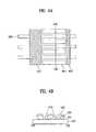
- FIG. 4Ais an enlarged view of “C” portion of FIG. 3 so as to explain a sealant and a dummy column spacer in a liquid crystal display device according to the first embodiment of the present invention
- FIG. 4Bis a cross-sectional view of a liquid crystal display device taken along line IVB-IVB of FIG. 4A;
- FIG. 5is an enlarged view of “B” portion of FIG. 3 so as to explain a dummy column spacer in a liquid crystal display device according to a second embodiment of the present invention
- FIG. 6is an enlarged view of “B” portion of FIG. 3 so as to explain a dummy column spacer in a liquid crystal display device according to a third embodiment of the present invention
- FIG. 7is an enlarged view of “B” portion of FIG. 3 so as to explain a dummy column spacer in a liquid crystal display device according to a fourth embodiment of the present invention
- FIG. 8is a cross-sectional view of an in-plane switching mode liquid crystal display device taken along line A-A of FIG. 3 according to a fifth embodiment of the present invention.
- FIG. 9is a cross-sectional view of an in-plane switching mode liquid crystal display device taken along line A-A of FIG. 3 according to a sixth embodiment of the present invention.
- FIG. 10is a cross-sectional view of an in-plane switching mode liquid crystal display device taken along line A-A of FIG. 3 according to a seventh embodiment of the present invention.
- FIG. 11is a cross-sectional view of an in-plane switching mode liquid crystal display device taken along line A-A of FIG. 3 according to a eighth embodiment of the present invention.
- FIG. 12is a cross-sectional view of a TN mode liquid crystal display device taken along line A-A of FIG. 3 according to a ninth embodiment of the present invention.
- FIG. 13is a cross-sectional view of a TN mode liquid crystal display device taken along line A-A of FIG. 3 according to a tenth embodiment of the present invention.
- FIGS. 14A to 14 Gare cross-sectional views illustrating process steps of fabricating a liquid crystal display device according to a liquid crystal dispensing method of the present invention.
- FIG. 3is a plane view of a liquid crystal display device according to a liquid crystal dispensing method of a first embodiment of the present invention.
- FIG. 4Ais an enlarged view of “C” portion of FIG. 3 so as to explain a sealant and a dummy column spacer in the liquid crystal display device according to the first embodiment of the present invention.
- FIG. 4Bis a cross-sectional view of the liquid crystal display device taken along line IVB-IVB of FIG. 4A.
- a plurality of gate and data lines 380 and 390are formed to cross one another in an active region 420 of a thin film transistor array substrate (a first substrate) 400 , thereby forming a plurality of pixel regions.
- a pixel electrode 412is formed at each pixel region, and a plurality of thin film transistors (not shown) are formed at each crossing point of the gate and data lines 380 and 390 so as to apply signals of the data lines to each pixel electrode 412 according to signals of the gate lines.
- a liquid crystal(not shown) is dispensed on the first substrate 400 .
- the thin film transistor array substrate 400has a plurality of liquid crystal panels regions, each having an active region and a dummy region.
- a black matrix layer 430 , column spacers, and a photo-hardening sealant 410are formed on the surface of a color filter array substrate (a second substrate) 450 , which faces to the first substrate.
- the color filter array substrate 450has a plurality of liquid crystal display panel regions, each having an active region and a dummy region.
- the black matrix layer 430is formed outside the active region 420 on the second substrate 450 (for example, in the periphery of the active layer).
- the column spacers 405are formed in the active region 420 of the second substrate 450 so as to maintain a cell gap between the first and second substrates 400 and 450 .
- the photo-hardening sealant 410is formed outside and surrounds the black matrix layer 430 so as to attach the first and second substrates 400 and 450 to each other. Then, a dummy column spacer 425 is formed on the black matrix layer 430 .
- the column spacers 405 and the dummy column spacer 425are made of an organic resin material or a photosensitive material.
- the column spacers 405are formed on the second substrate 450 to correspond to the gate and data lines of the first substrate 400 except for the pixel regions to have a thickness in the range of about 5 and 30 ⁇ .
- the photo-hardening sealant 410may shrink during hardening, so that a mixture of a photo-hardening sealant and a thermo-hardening sealant may be used instead of using a single photo-hardening sealant. Also, the sealant 410 may be wider or narrower than the black matrix layer 430 in width.
- the dummy column spacer 425has openings to effectively regulate a liquid crystal flow. For example, there may be openings at three corner regions of the second substrate 450 and no opening at one corner region. Each opening has a different size.
- the liquid crystalflows toward three corner regions B 1 , B 2 , and B 3 of the second substrate 450 from the one corner region without an opening.
- the liquid crystalflows toward the two corner regions B 2 and B 3 of the second substrate 450 from the corner region B 1 having an opening smaller than those of the regions B 2 and B 3 .
- the liquid crystalflows toward the one of the two corner regions B 2 and B 3 of the second substrate 450 from whichever the corner region having a smaller sized opening.
- the liquid crystalflows out of the liquid crystal display panel at the corner region having the largest sized opening, thereby forming a uniform liquid crystal layer.
- the first and second substrates 400 and 450are attached to each other with the photo-hardening sealant 410 .
- UV-rayis irradiated to the first and second substrate from a top of the second substrate 450 so as to harden the photo-hardening sealant 410 , thereby bonding the first and second substrates 400 and 450 to each other.
- a gate insulating layer 481 and a passivation layer 482are selectively removed between the photo-hardening sealant 410 and the dummy column spacer 425 , thereby forming a buffer region 490 for filling a liquid crystal therein.
- portions of the gate insulating layer 481 and the passivation layer 482are selectively removed between the gate and data lines of the first substrate 400 .
- the buffer region 490is used as a space to accommodate the liquid crystal when the liquid crystal is excessively dispensed on the substrate. If the amount of the liquid crystal on the substrate is not enough, the buffer region 490 acts to guide the liquid crystal.
- the dummy column spacermay be formed in a different way in the liquid crystal display device having the aforementioned structure according to the first embodiment of the present invention.
- FIG. 5is an enlarged view of “B” portion of FIG. 3 so as to explain a dummy column spacer in a liquid crystal display device according to a second embodiment of the present invention.
- a dummy column spacer 416 for regulating a liquid crystal flowis formed on a black matrix layer 430
- an alignment layer 414is formed on the second substrate 450 including the dummy column spacer 416 .
- the dummy column spacer 416is formed to have a plurality of openings 417 and is made of an organic resin material or a photosensitive material.
- the dummy column spacer 416may be formed with the column spacer 405 simultaneously, or separately.
- an overcoat layermay be formed on the black,matrix layer 430 , and the dummy column spacer 416 may be formed on the overcoat layer.
- a buffer regionis formed by removing portions of the gate insulating layer and/or the passivation layer between the dummy column spacer 416 and the sealant 410 .
- a liquid crystalis dispensed on the substrate and spreads out, it moves to the buffer region through the openings, thereby preventing generation of bubbles even when the liquid crystal is slowly filled.
- the liquid crystalis excessively dispensed on the substrate, it is guided to the buffer region through the openings, thereby maintaining a uniform cell gap.
- the dummy column spacer 416is formed between the active region 420 and the photo-hardening sealant 410 , so that it prevents external substance generated by the photo-hardening sealant 410 from penetrating into the active region 420 .
- FIG. 6is an enlarged view of “B” portion of FIG. 3 so as to explain a dummy column spacer in a liquid crystal display device according to the third embodiment of the present invention.
- the dummy column spacer 416 having the plurality of openings 417is formed on the black matrix layer 430 so as to regulate the liquid crystal flow, and dotted column spacers 415 are formed outside the dummy column space 416 toward the sealant 410 .
- the alignment layer 414is formed on the substrate including the dummy column spacer 416 and the dotted column spacers 415 .
- the dummy column spacer 416 and the dotted column spacers 415are made of an organic resin material, which may be formed simultaneously or separately.
- the openings 417may be formed successively or not.
- the buffer regionis formed between the dotted column spacers 415 and the sealant 410 by removing portions of the gate insulating layer and the passivation layer.
- the dotted column spacer 415are additionally formed to the dummy column spacer 416 having the openings at corner regions, thereby regulating the liquid crystal flow more effectively. Furthermore, it prevents foreign substance generated by the photo-hardening sealant 410 from penetrating into the active region 420 .
- FIG. 7is an enlarged view of “B” portion of FIG. 3 so as to explain a dummy column spacer in a liquid crystal display device according to the fourth embodiment of the present invention.
- the dummy column space 416 having the openings 417is formed on the black matrix layer 430 so as to regulate the liquid crystal flow, and dotted column spacers 415 are formed inside the dummy column spacer 416 toward the active region 420 .
- the alignment layer 414is formed on the second substrate including the dummy column spacer 416 and the dotted column spacers 415 .
- An overcoat layer(not shown) may be formed on the black matrix layer 430 , and then the dummy column spacer 416 and the dotted column spacers 415 may be formed on the overcoat layer. At this time, the dummy column spacer 416 and the dotted column spacers 415 of an organic resin material may be formed simultaneously or separately.
- the openings 417may be formed successively or not.
- the buffer regionis formed between the dotted column spacers 415 and the sealant 410 by selectively removing portions of the gate insulating layer and the passivation layer.
- the dotted column spacers 415are additionally formed to the dummy column spacer 416 , thereby regulating the liquid crystal flow more effectively. In addition, it prevents foreign substances generated by the photo-hardening sealant 410 from penetrating into the active region 420 .
- the dummy column spacer for regulating the liquid crystal flowvaries with a different structure according to the mode of the liquid crystal display device.
- FIG. 8An in-plane switching mode liquid crystal display device according to a fifth embodiment of the present invention will be explained with reference to FIG. 8.
- a metal layeris deposited on the first substrate 400 , and a common electrode 313 and a gate line (not shown) having a gate electrode 309 are formed on the first substrate 400 by photolithography.
- a gate insulating layer 320is formed on the entire surface of the first substrate 400 including the gate electrode 309 and the common electrode 313 .
- a semiconductor layer 315is formed on the gate insulating layer 320 on the gate electrode 309 .
- the data line 390 having source and drain electrodes 316 and 317 on both sides of the semiconductor layer 315is formed on the gate insulating layer 320 , and a pixel electrode 314 is formed in parallel to the common electrode 313 for being connected to the drain electrode in a pixel region.
- a passivation layer 325is formed on the first substrate 400 including the pixel electrode 314 , and the buffer region 490 is formed by selectively removing portions of the gate insulating layer 320 and the passivation layer 325 between the sealant 410 and the dummy column spacer 416 / 425 with a mask.
- a first alignment layer 331is formed on the passivation layer 325 .
- the black matrix layer 430 and a color filter layer 322are formed on the second substrate 450 , and an overcoat layer 323 is formed on the entire surface of the second substrate 450 so as to reduce a step coverage between the black matrix layer 430 and the color filter layer 322 .
- the overcoat layer 323is formed of one of Cr, CrOx, and black resin.
- the column spacer 405is formed in the active region of the second substrate 450 , and the dummy column spacer 416 / 425 is formed in the periphery (i.e., the outside) of the active region on the overcoat layer 323 .
- the second alignment layer 414is formed on the column spacer 405 and the dummy column spacer 425 , and then the photo-hardening sealant 410 is deposited thereon.
- the liquid crystalis dispensed on the first substrate 400 having the alignment layer, and the second substrate 450 is positioned above the first substrate 400 .
- the first and second substrates 400 and 450are attached to each other. At this time, the sealant may be formed on the first substrate 400 .
- the overcoat layer 323is removed from the second substrate corresponding to the photo-hardening sealant 410 .
- the overcoat layer 323is formed on the entire surface of the second substrate including the photo-hardening sealant 410 in the in-plane switching mode liquid crystal display device according to a sixth embodiment of the present invention, as shown in FIG. 9.
- the black matrix layer 430 and the color filter layer 322are formed on the second substrate 450 , and the overcoat layer 323 is formed on the entire surface of the second substrate 450 so as to reduce a step coverage between the black matrix layer 430 and the color filter layer 322 .
- the column spacer 405 and the dummy column spacer 416 / 425are respectively formed in the active region and the periphery (i.e., the outside) of the active region without patterning the overcoat layer 323 .
- the second alignment layer 414is formed on the column spacer 405 and the dummy column spacer 416 / 425 , and the photo-hardening sealant 410 is deposited on one of the first and second substrates 400 and 450 . After dispensing the liquid crystal on the first substrate 400 , the second substrate 450 is disposed on the first substrate 400 .
- the in-plane switching mode liquid crystal display devicehas same structure as that according to the fifth and sixth embodiments of the present invention except for that the overcoat layer 323 is patterned on the substrate and a dummy color filter layer 322 a is connected to the overcoat layer 323 .
- the in-plane switching mode liquid crystal display devicehas same structure as that according to the fifth embodiment of the present invention except for that there is a gap between the dummy column spacer 416 / 425 and the first substrate 400 .
- the liquid crystalflows into the buffer region 490 between the photo-hardening sealant 410 and the dummy column spacer 416 / 425 in the active region 420 since the gap is formed between the dummy column spacer and the first substrate, thereby regulating the liquid crystal flow.
- the buffer region 490is formed by selectively removing portions of the gate insulating layer 320 and the passivation layer 325 between the dummy column spacer 416 / 425 and the photo-hardening sealant 410 .
- the common electrode 313may be formed on the different layer from the pixel electrode 314 , or both of them may be formed on the gate insulating layer 320 or on the same layer as the source and drain electrode 316 and 317 . Also, the common electrode 313 may be formed on the same layer as the gate electrode 309 , and the pixel electrode 314 may be formed on the passivation layer 325 . The common electrode 313 and the pixel electrode 314 may be formed on the passivation layer 325 . Accordingly, the common electrode 313 and pixel electrode 314 may be disposed in various ways.
- both the gate insulating layer 320 and the passivation layer 325may be removed, or only passivation layer 325 may be removed.
- the buffer region 490is formed by removing the passivation layer 325 between the sealant 410 and the dummy column spacer 416 / 425 so as to connect the pixel electrode 314 to the drain electrode 317 of the thin film transistor when a contact hole is formed in the passivation layer 325 .
- the buffer region 490may be additionally formed with a mask.
- FIG. 12is a cross-sectional view of a TN mode liquid crystal display device taken along line A-A of FIG. 3 according to a ninth embodiment of the present invention.
- FIG. 13is a cross-sectional view of a TN mode liquid crystal display device taken along line A-A of FIG. 3 according to a tenth embodiment of the present invention.
- the TN mode liquid crystal display devicewill be explained with reference to FIG. 12.
- a metal layeris deposited on the first substrate 400 , and the gate line 380 having the gate electrode 309 is formed on the first substrate 400 by photolithography.
- the gate insulating layer 320is formed on the entire surface of the first substrate 400 including the gate electrode 309 and the gate line 380 .
- the semiconductor layer 315is formed on the gate insulating layer 320 above the gate electrode 309 , and a data line (not shown) having the source and drain electrodes 316 and 317 on both sides of the semiconductor layer 315 is formed on the first substrate 400 .
- the passivation layer 325is formed on the entire surface of the first substrate 400 including the source and drain electrodes 316 and 317 . After forming a contact hole on the drain electrode 317 , the pixel electrode 314 is formed in the pixel region for being connected to the drain electrode 317 through the contact hole. At this time, portions of the gate insulating layer 320 and the passivation layer 325 between the sealant 410 and the dummy column spacer 416 / 425 are selectively removed during forming the contact hole, thereby forming the buffer region 490 .
- the buffer region 375may be formed by removing only the passivation layer 325 .
- the first alignment layer 331is formed on the entire surface of the first substrate 400 including the pixel electrode 314 .
- the second substrate 450includes the black matrix layer 430 , the color filter layers 322 , the common electrode 326 and the photo-hardening sealant 410 .
- the black matrix layers 430are formed on the second substrate in order to prevent light leakage out of the liquid crystal display panel, and the color filter layers are formed between the black matrix layers 430 .
- the common electrode 326is formed on the entire surface of the second substrate 450 including the color filter layer 322 and the black matrix layer 430 . Thereafter, the column spacer 405 is formed in the active region 420 of the second substrate 450 .
- the dummy column spacers 416 / 425are formed on the common electrode 326 in the periphery (i.e., the outside) of the active region 420 .
- the second alignment layer 414is formed on the column spacer 405 and the dummy column spacer 425 , and the photo-hardening sealant 410 is deposited in the periphery of the dummy column spacer 416 / 425 .
- the liquid crystalis dispensed on the first substrate 400 having the alignment layer, and the second substrate 450 is disposed on the first substrate 400 so as to attach the first and second substrates to each other.
- the embodiments of the present inventionmay be applied to various modes of the liquid crystal display, such as a vertical alignment (VA) mode, an optically controlled birefringence (OCB) mode, a ferroelectric liquid crystal (FLC) mode, and a reflective type mode.
- VAvertical alignment
- OBCoptically controlled birefringence
- FLCferroelectric liquid crystal
- the overcoat layermay be formed on the color filter layer 322 .
- the TN mode liquid crystal display devicehas same structure as that according to the ninth embodiment of the present invention except for that a gap is formed between the dummy column spacer 416 / 425 and the first substrate 400 with the predetermined gap. Accordingly, the liquid crystal flows into the buffer region 490 between the photo-hardening sealant 410 and the dummy column spacer 416 / 425 in the active region 420 , thereby regulating the liquid crystal flow 413 . At this time, the buffer region 490 is formed by selectively removing portions of the gate insulating layer 320 and the passivation layer 325 between the dummy column spacer 416 / 425 and the photo-hardening sealant 410 .
- a method of fabricating a liquid crystal display panel by using a liquid crystal dispensing methodwill be explained with reference to FIGS. 14A to 14 G.
- a plurality of liquid crystal display panel regionsare formed on the first and second substrates, and then a thin film transistor array and a color filter array are respectively formed on the substrates.
- the substrateis cut into unit liquid crystal display panel regions.
- a plurality of gate and data linesare formed to cross one another on the first substrate 400 , thereby defining a plurality of pixel regions.
- a pixel electrode(not shown) is formed at each pixel region, and a plurality of thin film transistors (not shown) are formed at each crossing point of the gate and data lines for applying signals of the data lines to each pixel electrode according to signals of the gate lines.
- a common line pattern(not shown) is formed for applying a voltage to a common electrode.
- a plurality of liquid crystal display panel regions 399are formed on the substrate.
- a plurality of silver (Ag) dots 401are formed on the common line pattern of each liquid crystal display panel region for being electrically connected to the common line pattern, and a liquid crystal 403 is appropriately dispensed on each liquid crystal display panel region 399 .
- a black matrix layer(not shown), a color filter layer (not shown), and a common electrode (not shown) are formed on the second substrate 450 .
- a column spacer 405is formed on each liquid crystal display panel region 399 of the second substrate corresponding to the gate and data lines of the first substrate 400 .
- the photo-hardening sealant 410is deposited in the periphery of each liquid crystal display panel region 399 ,of the second substrate 450 , as shown in FIG. 14C.
- the first substrateis positioned at the lower part, and the second substrate is disposed over the first substrate 400 .
- the first and second substrates 400 and 450are loaded to a bonding apparatus having a controllable vacuum chamber.
- the second substrate 450is fixed to an upper stage 470 that moves along the Z-axis direction (i.e., vertical direction).
- the first substrate 400is fixed to a lower stage 460 that moves along the XY-axis direction (i.e., horizontal direction). Subsequently, as shown in FIG.
- the second substrate 450 fixed to the upper stage 470 and the first substrate fixed to the lower stage 460are aligned, and the chamber of the bonding apparatus becomes in a vacuum condition, thereby attaching the first and second substrates 400 and 450 to each other.
- the first and second substratesare attached to each other with a first gap.
- gas or dry airis provided to the chamber of the bonding apparatus under a vacuum condition so as to make a pressure of the chamber to the atmospheric pressure. Accordingly, the first and second substrates 400 and 450 attached by the sealant 410 are maintained under a vacuum condition, and the circumferential region of the substrates become under the atmospheric pressure, so that the first and second substrates are pressed to each other due to a pressure difference between the inside pressure of the substrates 400 and 450 and the atmospheric pressure. Simultaneously, the liquid crystal 403 spreads out on the entire liquid crystal display panel between the first and second substrates 400 and 450 , thereby forming a liquid crystal layer 403 a. After that, the UV-ray is irradiated to only photo-hardening sealant from the top of the second substrate 450 so as to harden the photo-hardening sealant 410 , as shown in FIG. 14G.
- the liquid crystal display device and method of fabricating the sameit is possible to form the liquid crystal, the sealant, the column spacer, the and dummy column spacer on any one of the first and second substrates.
- the substrate having the liquid crystalis disposed at the lower stage of the bonding apparatus, and the other substrate is disposed at the upper stage of the bonding apparatus.
- the liquid crystal display device and method of fabricating the samehas the following advantages.
- the buffer regionis formed by removing portions of the gate insulating layer and the passivation layer between the dummy column spacer and the sealant, so as to regulate the liquid crystal flow. If the liquid crystal is excessively dispensed on the substrate, the liquid crystal flows into the buffer region, thereby accommodating the liquid crystal on the liquid crystal display panel appropriately. Meanwhile, if the amount of the liquid crystal on the substrate is not enough, the liquid crystal moves from other regions to the buffer region, thereby filling the liquid crystal on the liquid crystal display panel appropriately.
Landscapes
- Physics & Mathematics (AREA)
- Nonlinear Science (AREA)
- Mathematical Physics (AREA)
- Chemical & Material Sciences (AREA)
- Crystallography & Structural Chemistry (AREA)
- General Physics & Mathematics (AREA)
- Optics & Photonics (AREA)
- Liquid Crystal (AREA)
Abstract
Description
- This application claims the benefit of the Korean Patent Application No. P2001-082739 filed on Dec. 21, 2001, which is hereby incorporated by reference.[0001]
- 1. Field of the Invention[0002]
- The present invention relates to a display device, and more particularly, to a liquid crystal display device and a method of fabricating the same. Although the present invention is suitable for a wide scope of applications, it is particularly suitable for effectively controlling liquid crystal flow in fabricating a liquid crystal display.[0003]
- 2. Discussion of the Related Art[0004]
- In general, applications of liquid crystal display devices have characteristics, such as full color realization, low voltage operation, low power consumption, thinness, lightness in weight, and high image quality. Thus, its applications have been diversified from monitors for electronic watches, calculators, notebook computers, personal computers and TV's, and monitors for aviation gauges, personal digital assistants (PDA's), and mobile stations.[0005]
- A method of forming a liquid crystal layer is largely classified into two methods, such as a liquid crystal injection method and a liquid crystal dispensing method. As a panel of the liquid crystal display device becomes larger in size, the liquid crystal dispensing method is mostly used in fabricating the liquid crystal display device. This is because the liquid crystal injection method takes more time to inject the liquid crystal between first and second substrates. In the liquid crystal dispensing method, liquid crystal droplets are dispensed on one of the first and second substrates, and then the substrates are bonded to each other to form the liquid crystal layer.[0006]
- When the liquid crystal is injected between the first and second substrates, a thermo-hardening sealant is usually used. For instance, epoxy resin is mixed with amine or amide in order to form a thermo-hardening sealant. The thermo-hardening sealant is hardened by applying heat to the sealant for about one or two hours at a temperature of about 100□, so that contamination of the liquid crystal may occur due to a long hardening time period. In the liquid crystal dispensing method, the first and second substrates are attached to each other with a photo-hardening sealant. In this case, the photo-hardening sealant is a mixture of a hardener and acryl resin. When UV-ray is irradiated to the sealant, the hardener becomes a radical, and then the radical acts with the acryl resin, so that the acryl resin is activated. Accordingly, the mixture is polymerized so that adhesion of the sealant is improved. After forming the liquid crystal layer between the first and second substrates, the UV-ray is irradiated to the attached substrates in order to harden the sealant between the first and second substrates for several seconds. In addition, a ball spacer is used between the first and second substrates so as to maintain a cell gap in the liquid crystal injection method. Meanwhile, a column spacer is used between the first and second substrates so as to maintain a cell gap in the liquid crystal dispensing method.[0007]
- A related art liquid crystal display device and a method of fabricating the same will be explained with reference to the accompanying drawings.[0008]
- FIG. 1 is a plane view of a liquid crystal display device according to a related art liquid crystal dispensing method. FIGS. 2A to[0009]2G are plane views illustrating process steps of fabricating a liquid crystal display device according to a related art liquid crystal dispensing method.
- In FIG. 1, a plurality of[0010]
gate lines 80 and a plurality ofdata lines 90 are formed to cross one another in anactive region 120 of a thin film transistor array substrate (i.e., a first substrate)100, thereby defining a plurality of pixel regions. Apixel electrode 112 is formed at each pixel region. A plurality of thin film transistors (not shown) are formed at each corresponding crossing point of the gate anddata lines pixel electrode 112 according to signals of the gate lines. Then, the liquid crystal (not shown) is dispensed on thefirst substrate 100. - Next, a color filter array substrate (i.e., a second substrate)[0011]150 includes column spacers, a
black matrix layer 130, and a photo-hardening sealant. In this case, thecolumn spacers 105 are formed on thesecond substrate 150 so as to maintain a cell gap between the first andsecond substrates black matrix layer 130 is formed in the periphery of theactive region 120. The photo-hardeningsealant 110 surrounding theblack matrix layer 130 is formed in the periphery of theblack matrix layer 130 so as to attach the first andsecond substrates second substrates sealant 110, UV-ray is irradiated to the attached substrates from the top of thesecond substrate 150 for hardening the photo-hardeningsealant 110, thereby bonding the first and second substrates to each other. - At this time, there may occur imperfect or excessive filling of the liquid crystal if the exact amount of the liquid crystal is not dispensed on the substrates. When the amount of the liquid crystal dispensed on the substrate is less than the required amount, it takes time to spread the liquid crystal from the center of the substrate to the corner regions, such as the farthest spots. As a result, a tilt angle of the liquid crystal may be changed since a contaminant is accumulated on the liquid crystal display panel. On the other hand, when too much liquid crystal is dispensed on the substrate, spots may appear on the liquid crystal display panel due to a problem in the spacer for maintaining a cell gap between the first and second substrates.[0012]
- A method of fabricating a liquid crystal display device according to a related art liquid crystal dispensing method will be explained in detail.[0013]
- FIGS. 2A to[0014]2G are plane views illustrating fabricating process steps of a liquid crystal display device according to a related art liquid crystal dispensing method. In the liquid crystal display device according to the related art liquid crystal dispensing method, a plurality of liquid crystal display panel regions are formed on first and second substrates. A thin film transistor array and a color filter array are respectively formed on the first and second substrates. Then, a liquid crystal is dispensed on the substrate, and a sealant is deposited thereon. After attaching the substrates to each other, each substrate is cut into unit liquid crystal display panel regions, thereby forming the liquid crystal display panel regions on each substrate.
- More specifically, in FIG. 2A, a plurality of gate lines (not shown) are formed on the[0015]
first substrate 100, and a plurality of data lines (not shown) are formed on thefirst substrate 100 to cross one another, thereby defining a plurality of pixel regions. A pixel electrode (not shown) is formed at each pixel region, and the thin film transistors (not shown) are formed at each crossing point of the gate and data lines for applying signals of the data lines to each pixel electrode according to signals of the gate lines. Also, a common line (not shown) is formed for applying a voltage to a common electrode. In this case, a plurality of liquid crystaldisplay panel regions 99 are formed on thefirst substrate 100. Then, a plurality of silver (Ag)dots 101 are formed on the common line of each liquid crystaldisplay panel region 99 to provide an electrical connection to the common line. Theliquid crystal 103 is appropriately dispensed on each liquid crystaldisplay panel region 99 of thefirst substrate 100. - As shown in FIG. 2B, a black matrix layer (not shown), a color filter layer (not shown), and a common electrode (not shown) are formed on the[0016]
second substrate 150. Acolumn spacer 105 is formed on each liquid crystaldisplay panel region 99 of thesecond substrate 150 corresponding to the gate and data lines of thefirst substrate 100. Then, a photo-hardeningsealant 110 is formed in the periphery of each liquid crystaldisplay panel region 99 of thesecond substrate 150, as shown in FIG. 2C. - In FIG. 2D, the[0017]
first substrate 100 is placed under thesecond substrate 150. The first andsecond substrates second substrate 150, on which thesealant 110 is deposited, faces down, and then is fixed to anupper stage 170 that moves along the Z-axis direction (i.e., vertical direction). Also, thefirst substrate 100 is fixed to alower stage 160 that moves along the XY-axis direction (i.e., horizontal direction). After that, thesecond substrate 150 fixed to theupper stage 170 and the first substrate fixed to thelower stage 160 are aligned, and the chamber of the bonding apparatus is in a vacuum condition, thereby attaching the first andsecond substrates - Subsequently, as shown in FIG. 2F, gas or dry air is provided to the chamber of the bonding apparatus under a vacuum condition so as to equalize the pressure of the chamber with the atmospheric pressure. Accordingly, the first and second substrates attached by the[0018]
sealant 110 are maintained under vacuum, and the circumferential area of the substrates is under the atmospheric pressure, so that the first and second substrates are pressed to each other due to a pressure difference between the inside pressure of the substrates and the atmospheric pressure. Simultaneously, theliquid crystal 103 spreads out on the entire liquid crystal display panel between the first and second substrates, thereby forming aliquid crystal layer 103a.Then, the UV-ray is irradiated to the attached substrates from the top of thesecond substrate 150, thereby hardening the photo-hardeningsealant 110. - However, the related art liquid crystal display device according to the liquid crystal dispensing method and the method of fabricating the same have the following disadvantages.[0019]
- When the dispensed amount of the liquid crystal is too much on the substrate, a uniform cell gap cannot be maintained between the first and second substrates since a buffer region, in which the liquid crystal may move around, cannot be formed in the liquid crystal display device when the substrates are attached to each other. On the other hand, when the dispensed amount of the liquid crystal is not enough on the substrate, it is difficult to regulate the liquid crystal flow in the related art liquid crystal display device since the buffer region cannot be formed therein.[0020]
- Accordingly, the present invention is directed to a liquid crystal display device and a method of fabricating the same that substantially obviates one or more of problems due to limitations and disadvantages of the related art.[0021]
- Another object of the present invention is to provide a liquid crystal display device and a method of fabricating the same that enables to regulate a liquid crystal flow even when the dispensed amount of the liquid crystal is too excessive or not enough on the liquid crystal panel.[0022]
- Additional features and advantages of the invention will be set forth in the description which follows and in part will be apparent from the description, or may be learned by practice of the invention. The objectives and other advantages of the invention will be realized and attained by the structure particularly pointed out in the written description and claims hereof as well as the appended drawings.[0023]
- To achieve these and other advantages and in accordance with the purpose of the present invention, as embodied and broadly described, a liquid crystal display device includes first and second substrates including a plurality of liquid crystal display panel regions, each liquid crystal display panel region having an active region and a dummy region, a sealant outside the liquid crystal display panel regions, a dummy column spacer on the dummy region to control a liquid crystal flow, a buffer region between the sealant and the dummy column spacer to accommodate a liquid crystal, and a liquid crystal layer between the first and second substrates.[0024]
- In another aspect of the present invention, a method of fabricating a liquid crystal display device includes forming a buffer region at a dummy region of a plurality of liquid crystal display panel regions on a first substrate, each liquid crystal display panel region having active and dummy regions, forming a liquid crystal on the active region, forming a dummy column spacer for controlling a liquid crystal flow on a dummy region of a plurality of liquid crystal display panel regions on a second substrate, each liquid crystal display panel region having active and dummy regions, forming a sealant outside the liquid crystal display panel region of one of the first and second substrates, and bonding the first and second substrates.[0025]
- It is to be understood that both the foregoing general description and the following detailed description are exemplary and explanatory and are intended to provide further explanation of the invention as claimed.[0026]
- The accompanying drawings, which are included to provide a further understanding of the invention and are incorporated in and constitute a part of this application, illustrate embodiments of the invention and together with the description serve to explain the principle of the invention.[0027]
- In the drawings:[0028]
- FIG. 1 is a plane view of a liquid crystal display device according to a related art liquid crystal dispensing method;[0029]
- FIGS. 2A to[0030]2G are cross-sectional views illustrating process steps of fabricating a liquid crystal display device according to the related art liquid crystal dispensing method;
- FIG. 3 is a plane view of a liquid crystal display device according to a liquid crystal dispensing method of the first embodiment of the present invention;[0031]
- FIG. 4A is an enlarged view of “C” portion of FIG. 3 so as to explain a sealant and a dummy column spacer in a liquid crystal display device according to the first embodiment of the present invention;[0032]
- FIG. 4B is a cross-sectional view of a liquid crystal display device taken along line IVB-IVB of FIG. 4A;[0033]
- FIG. 5 is an enlarged view of “B” portion of FIG. 3 so as to explain a dummy column spacer in a liquid crystal display device according to a second embodiment of the present invention;[0034]
- FIG. 6 is an enlarged view of “B” portion of FIG. 3 so as to explain a dummy column spacer in a liquid crystal display device according to a third embodiment of the present invention;[0035]
- FIG. 7 is an enlarged view of “B” portion of FIG. 3 so as to explain a dummy column spacer in a liquid crystal display device according to a fourth embodiment of the present invention;[0036]
- FIG. 8 is a cross-sectional view of an in-plane switching mode liquid crystal display device taken along line A-A of FIG. 3 according to a fifth embodiment of the present invention;[0037]
- FIG. 9 is a cross-sectional view of an in-plane switching mode liquid crystal display device taken along line A-A of FIG. 3 according to a sixth embodiment of the present invention;[0038]
- FIG. 10 is a cross-sectional view of an in-plane switching mode liquid crystal display device taken along line A-A of FIG. 3 according to a seventh embodiment of the present invention;[0039]
- FIG. 11 is a cross-sectional view of an in-plane switching mode liquid crystal display device taken along line A-A of FIG. 3 according to a eighth embodiment of the present invention;[0040]
- FIG. 12 is a cross-sectional view of a TN mode liquid crystal display device taken along line A-A of FIG. 3 according to a ninth embodiment of the present invention;[0041]
- FIG. 13 is a cross-sectional view of a TN mode liquid crystal display device taken along line A-A of FIG. 3 according to a tenth embodiment of the present invention; and[0042]
- FIGS. 14A to[0043]14G are cross-sectional views illustrating process steps of fabricating a liquid crystal display device according to a liquid crystal dispensing method of the present invention.
- Reference will now be made in detail to the illustrated embodiments of the present invention, examples of which are illustrated in the accompanying drawings. Wherever possible, the same reference numbers will be used throughout the drawings to refer to the same or like parts.[0044]
- FIG. 3 is a plane view of a liquid crystal display device according to a liquid crystal dispensing method of a first embodiment of the present invention. FIG. 4A is an enlarged view of “C” portion of FIG. 3 so as to explain a sealant and a dummy column spacer in the liquid crystal display device according to the first embodiment of the present invention. FIG. 4B is a cross-sectional view of the liquid crystal display device taken along line IVB-IVB of FIG. 4A.[0045]
- As shown in FIG. 3, a plurality of gate and[0046]
data lines active region 420 of a thin film transistor array substrate (a first substrate)400, thereby forming a plurality of pixel regions. Apixel electrode 412 is formed at each pixel region, and a plurality of thin film transistors (not shown) are formed at each crossing point of the gate anddata lines pixel electrode 412 according to signals of the gate lines. Then, a liquid crystal (not shown) is dispensed on thefirst substrate 400. The thin filmtransistor array substrate 400 has a plurality of liquid crystal panels regions, each having an active region and a dummy region. - Subsequently, a[0047]
black matrix layer 430, column spacers, and a photo-hardeningsealant 410 are formed on the surface of a color filter array substrate (a second substrate)450, which faces to the first substrate. The colorfilter array substrate 450 has a plurality of liquid crystal display panel regions, each having an active region and a dummy region. At this time, theblack matrix layer 430 is formed outside theactive region 420 on the second substrate450 (for example, in the periphery of the active layer). The column spacers405 are formed in theactive region 420 of thesecond substrate 450 so as to maintain a cell gap between the first andsecond substrates sealant 410 is formed outside and surrounds theblack matrix layer 430 so as to attach the first andsecond substrates dummy column spacer 425 is formed on theblack matrix layer 430. In this case, thecolumn spacers 405 and thedummy column spacer 425 are made of an organic resin material or a photosensitive material. The column spacers405 are formed on thesecond substrate 450 to correspond to the gate and data lines of thefirst substrate 400 except for the pixel regions to have a thickness in the range of about 5 and 30□. The photo-hardeningsealant 410 may shrink during hardening, so that a mixture of a photo-hardening sealant and a thermo-hardening sealant may be used instead of using a single photo-hardening sealant. Also, thesealant 410 may be wider or narrower than theblack matrix layer 430 in width. - Also, the[0048]
dummy column spacer 425 has openings to effectively regulate a liquid crystal flow. For example, there may be openings at three corner regions of thesecond substrate 450 and no opening at one corner region. Each opening has a different size. Thus, the liquid crystal flows toward three corner regions B1, B2, and B3 of thesecond substrate 450 from the one corner region without an opening. Also, the liquid crystal flows toward the two corner regions B2 and B3 of thesecond substrate 450 from the corner region B1 having an opening smaller than those of the regions B2 and B3. The liquid crystal flows toward the one of the two corner regions B2 and B3 of thesecond substrate 450 from whichever the corner region having a smaller sized opening. And finally, the liquid crystal flows out of the liquid crystal display panel at the corner region having the largest sized opening, thereby forming a uniform liquid crystal layer. Subsequently, the first andsecond substrates sealant 410. Then, UV-ray is irradiated to the first and second substrate from a top of thesecond substrate 450 so as to harden the photo-hardeningsealant 410, thereby bonding the first andsecond substrates - As shown in FIGS. 4A and 4B, a[0049]
gate insulating layer 481 and apassivation layer 482 are selectively removed between the photo-hardeningsealant 410 and thedummy column spacer 425, thereby forming abuffer region 490 for filling a liquid crystal therein. In other words, portions of thegate insulating layer 481 and thepassivation layer 482 are selectively removed between the gate and data lines of thefirst substrate 400. At this time, thebuffer region 490 is used as a space to accommodate the liquid crystal when the liquid crystal is excessively dispensed on the substrate. If the amount of the liquid crystal on the substrate is not enough, thebuffer region 490 acts to guide the liquid crystal. The dummy column spacer may be formed in a different way in the liquid crystal display device having the aforementioned structure according to the first embodiment of the present invention. - FIG. 5 is an enlarged view of “B” portion of FIG. 3 so as to explain a dummy column spacer in a liquid crystal display device according to a second embodiment of the present invention. In the liquid crystal display device according to the second embodiment of the present invention, a[0050]
dummy column spacer 416 for regulating a liquid crystal flow is formed on ablack matrix layer 430, and analignment layer 414 is formed on thesecond substrate 450 including thedummy column spacer 416. Thedummy column spacer 416 is formed to have a plurality ofopenings 417 and is made of an organic resin material or a photosensitive material. Thedummy column spacer 416 may be formed with thecolumn spacer 405 simultaneously, or separately. Although not shown in FIG. 5, an overcoat layer may be formed on the black,matrix layer 430, and thedummy column spacer 416 may be formed on the overcoat layer. - In the liquid crystal display device according to the second embodiment of the present invention, a buffer region is formed by removing portions of the gate insulating layer and/or the passivation layer between the[0051]
dummy column spacer 416 and thesealant 410. When a liquid crystal is dispensed on the substrate and spreads out, it moves to the buffer region through the openings, thereby preventing generation of bubbles even when the liquid crystal is slowly filled. Also, when the liquid crystal is excessively dispensed on the substrate, it is guided to the buffer region through the openings, thereby maintaining a uniform cell gap. Thedummy column spacer 416 is formed between theactive region 420 and the photo-hardeningsealant 410, so that it prevents external substance generated by the photo-hardeningsealant 410 from penetrating into theactive region 420. - A dummy column spacer and column spacers according to a third embodiment of the present invention will be explained as follows. FIG. 6 is an enlarged view of “B” portion of FIG. 3 so as to explain a dummy column spacer in a liquid crystal display device according to the third embodiment of the present invention.[0052]
- Referring to FIG. 6, the[0053]
dummy column spacer 416 having the plurality ofopenings 417 is formed on theblack matrix layer 430 so as to regulate the liquid crystal flow, and dottedcolumn spacers 415 are formed outside thedummy column space 416 toward thesealant 410. Then, thealignment layer 414 is formed on the substrate including thedummy column spacer 416 and the dottedcolumn spacers 415. Thedummy column spacer 416 and the dottedcolumn spacers 415 are made of an organic resin material, which may be formed simultaneously or separately. Theopenings 417 may be formed successively or not. - As mentioned above, the buffer region is formed between the dotted[0054]
column spacers 415 and thesealant 410 by removing portions of the gate insulating layer and the passivation layer. In the liquid crystal display device according to the third embodiment of the present invention, the dottedcolumn spacer 415 are additionally formed to thedummy column spacer 416 having the openings at corner regions, thereby regulating the liquid crystal flow more effectively. Furthermore, it prevents foreign substance generated by the photo-hardeningsealant 410 from penetrating into theactive region 420. - A dummy column spacer and column spacers according to a fourth embodiment of the present invention will be explained as follows. FIG. 7 is an enlarged view of “B” portion of FIG. 3 so as to explain a dummy column spacer in a liquid crystal display device according to the fourth embodiment of the present invention. Referring to FIG. 7, the[0055]
dummy column space 416 having theopenings 417 is formed on theblack matrix layer 430 so as to regulate the liquid crystal flow, and dottedcolumn spacers 415 are formed inside thedummy column spacer 416 toward theactive region 420. Then, thealignment layer 414 is formed on the second substrate including thedummy column spacer 416 and the dottedcolumn spacers 415. An overcoat layer (not shown) may be formed on theblack matrix layer 430, and then thedummy column spacer 416 and the dottedcolumn spacers 415 may be formed on the overcoat layer. At this time, thedummy column spacer 416 and the dottedcolumn spacers 415 of an organic resin material may be formed simultaneously or separately. Theopenings 417 may be formed successively or not. - As mentioned above, the buffer region is formed between the dotted[0056]
column spacers 415 and thesealant 410 by selectively removing portions of the gate insulating layer and the passivation layer. In the liquid crystal display device according to the fourth embodiment of the present invention, the dottedcolumn spacers 415 are additionally formed to thedummy column spacer 416, thereby regulating the liquid crystal flow more effectively. In addition, it prevents foreign substances generated by the photo-hardeningsealant 410 from penetrating into theactive region 420. - The dummy column spacer for regulating the liquid crystal flow varies with a different structure according to the mode of the liquid crystal display device.[0057]
- An in-plane switching mode liquid crystal display device according to a fifth embodiment of the present invention will be explained with reference to FIG. 8. In FIG. 8, a metal layer is deposited on the[0058]
first substrate 400, and acommon electrode 313 and a gate line (not shown) having agate electrode 309 are formed on thefirst substrate 400 by photolithography. Agate insulating layer 320 is formed on the entire surface of thefirst substrate 400 including thegate electrode 309 and thecommon electrode 313. Then, asemiconductor layer 315 is formed on thegate insulating layer 320 on thegate electrode 309. - After that, the[0059]
data line 390 having source and drainelectrodes semiconductor layer 315 is formed on thegate insulating layer 320, and apixel electrode 314 is formed in parallel to thecommon electrode 313 for being connected to the drain electrode in a pixel region. Apassivation layer 325 is formed on thefirst substrate 400 including thepixel electrode 314, and thebuffer region 490 is formed by selectively removing portions of thegate insulating layer 320 and thepassivation layer 325 between thesealant 410 and thedummy column spacer 416/425 with a mask. Then, afirst alignment layer 331 is formed on thepassivation layer 325. - Next, the[0060]
black matrix layer 430 and acolor filter layer 322 are formed on thesecond substrate 450, and anovercoat layer 323 is formed on the entire surface of thesecond substrate 450 so as to reduce a step coverage between theblack matrix layer 430 and thecolor filter layer 322. At this time, theovercoat layer 323 is formed of one of Cr, CrOx, and black resin. - The[0061]
column spacer 405 is formed in the active region of thesecond substrate 450, and thedummy column spacer 416/425 is formed in the periphery (i.e., the outside) of the active region on theovercoat layer 323. Thesecond alignment layer 414 is formed on thecolumn spacer 405 and thedummy column spacer 425, and then the photo-hardeningsealant 410 is deposited thereon. Subsequently, the liquid crystal is dispensed on thefirst substrate 400 having the alignment layer, and thesecond substrate 450 is positioned above thefirst substrate 400. The first andsecond substrates first substrate 400. - In the in-plane switching mode liquid crystal display device according to the fifth embodiment of the present invention, a portion of the[0062]
overcoat layer 323 is removed from the second substrate corresponding to the photo-hardeningsealant 410. However, theovercoat layer 323 is formed on the entire surface of the second substrate including the photo-hardeningsealant 410 in the in-plane switching mode liquid crystal display device according to a sixth embodiment of the present invention, as shown in FIG. 9. - In detail, the[0063]
black matrix layer 430 and thecolor filter layer 322 are formed on thesecond substrate 450, and theovercoat layer 323 is formed on the entire surface of thesecond substrate 450 so as to reduce a step coverage between theblack matrix layer 430 and thecolor filter layer 322. Then, thecolumn spacer 405 and thedummy column spacer 416/425 are respectively formed in the active region and the periphery (i.e., the outside) of the active region without patterning theovercoat layer 323. Thesecond alignment layer 414 is formed on thecolumn spacer 405 and thedummy column spacer 416/425, and the photo-hardeningsealant 410 is deposited on one of the first andsecond substrates first substrate 400, thesecond substrate 450 is disposed on thefirst substrate 400. - Referring to FIG. 10, the in-plane switching mode liquid crystal display device according to a seventh embodiment of the present invention has same structure as that according to the fifth and sixth embodiments of the present invention except for that the[0064]
overcoat layer 323 is patterned on the substrate and a dummy color filter layer322ais connected to theovercoat layer 323. - Referring to FIG. 11, the in-plane switching mode liquid crystal display device according to an eighth embodiment of the present invention has same structure as that according to the fifth embodiment of the present invention except for that there is a gap between the[0065]
dummy column spacer 416/425 and thefirst substrate 400. The liquid crystal flows into thebuffer region 490 between the photo-hardeningsealant 410 and thedummy column spacer 416/425 in theactive region 420 since the gap is formed between the dummy column spacer and the first substrate, thereby regulating the liquid crystal flow. At this time, thebuffer region 490 is formed by selectively removing portions of thegate insulating layer 320 and thepassivation layer 325 between thedummy column spacer 416/425 and the photo-hardeningsealant 410. - As mentioned above, in the in-plane switching mode liquid crystal display devices according to the fifth, sixth, seventh, and eighth embodiments of the present invention, the[0066]
common electrode 313 may be formed on the different layer from thepixel electrode 314, or both of them may be formed on thegate insulating layer 320 or on the same layer as the source anddrain electrode common electrode 313 may be formed on the same layer as thegate electrode 309, and thepixel electrode 314 may be formed on thepassivation layer 325. Thecommon electrode 313 and thepixel electrode 314 may be formed on thepassivation layer 325. Accordingly, thecommon electrode 313 andpixel electrode 314 may be disposed in various ways. - During forming the[0067]
buffer region 490, both thegate insulating layer 320 and thepassivation layer 325 may be removed, or onlypassivation layer 325 may be removed. At this time, if thepixel electrode 314 is formed on thepassivation layer 325, thebuffer region 490 is formed by removing thepassivation layer 325 between thesealant 410 and thedummy column spacer 416/425 so as to connect thepixel electrode 314 to thedrain electrode 317 of the thin film transistor when a contact hole is formed in thepassivation layer 325. Thebuffer region 490 may be additionally formed with a mask. - FIG. 12 is a cross-sectional view of a TN mode liquid crystal display device taken along line A-A of FIG. 3 according to a ninth embodiment of the present invention. FIG. 13 is a cross-sectional view of a TN mode liquid crystal display device taken along line A-A of FIG. 3 according to a tenth embodiment of the present invention.[0068]
- The TN mode liquid crystal display device according to the ninth embodiment of the present invention will be explained with reference to FIG. 12. Referring to FIG. 12, a metal layer is deposited on the[0069]
first substrate 400, and thegate line 380 having thegate electrode 309 is formed on thefirst substrate 400 by photolithography. Then, thegate insulating layer 320 is formed on the entire surface of thefirst substrate 400 including thegate electrode 309 and thegate line 380. Thesemiconductor layer 315 is formed on thegate insulating layer 320 above thegate electrode 309, and a data line (not shown) having the source and drainelectrodes semiconductor layer 315 is formed on thefirst substrate 400. Thepassivation layer 325 is formed on the entire surface of thefirst substrate 400 including the source and drainelectrodes drain electrode 317, thepixel electrode 314 is formed in the pixel region for being connected to thedrain electrode 317 through the contact hole. At this time, portions of thegate insulating layer 320 and thepassivation layer 325 between thesealant 410 and thedummy column spacer 416/425 are selectively removed during forming the contact hole, thereby forming thebuffer region 490. The buffer region375 may be formed by removing only thepassivation layer 325. Thefirst alignment layer 331 is formed on the entire surface of thefirst substrate 400 including thepixel electrode 314. - The[0070]
second substrate 450 includes theblack matrix layer 430, the color filter layers322, thecommon electrode 326 and the photo-hardeningsealant 410. The black matrix layers430 are formed on the second substrate in order to prevent light leakage out of the liquid crystal display panel, and the color filter layers are formed between the black matrix layers430. Thecommon electrode 326 is formed on the entire surface of thesecond substrate 450 including thecolor filter layer 322 and theblack matrix layer 430. Thereafter, thecolumn spacer 405 is formed in theactive region 420 of thesecond substrate 450. Simultaneously, thedummy column spacers 416/425 are formed on thecommon electrode 326 in the periphery (i.e., the outside) of theactive region 420. Thesecond alignment layer 414 is formed on thecolumn spacer 405 and thedummy column spacer 425, and the photo-hardeningsealant 410 is deposited in the periphery of thedummy column spacer 416/425. The liquid crystal is dispensed on thefirst substrate 400 having the alignment layer, and thesecond substrate 450 is disposed on thefirst substrate 400 so as to attach the first and second substrates to each other. - The embodiments of the present invention may be applied to various modes of the liquid crystal display, such as a vertical alignment (VA) mode, an optically controlled birefringence (OCB) mode, a ferroelectric liquid crystal (FLC) mode, and a reflective type mode. As shown in FIGS.[0071]8 to10, the overcoat layer may be formed on the
color filter layer 322. - The TN mode liquid crystal display device according to the tenth embodiment of the present invention has same structure as that according to the ninth embodiment of the present invention except for that a gap is formed between the[0072]
dummy column spacer 416/425 and thefirst substrate 400 with the predetermined gap. Accordingly, the liquid crystal flows into thebuffer region 490 between the photo-hardeningsealant 410 and thedummy column spacer 416/425 in theactive region 420, thereby regulating theliquid crystal flow 413. At this time, thebuffer region 490 is formed by selectively removing portions of thegate insulating layer 320 and thepassivation layer 325 between thedummy column spacer 416/425 and the photo-hardeningsealant 410. - A method of fabricating a liquid crystal display panel by using a liquid crystal dispensing method will be explained with reference to FIGS. 14A to[0073]14G. A plurality of liquid crystal display panel regions are formed on the first and second substrates, and then a thin film transistor array and a color filter array are respectively formed on the substrates. On completing dispensing the liquid crystal and forming the sealant on the substrate, the substrate is cut into unit liquid crystal display panel regions.
- Referring to FIG. 14A, a plurality of gate and data lines (not shown) are formed to cross one another on the[0074]
first substrate 400, thereby defining a plurality of pixel regions. A pixel electrode (not shown) is formed at each pixel region, and a plurality of thin film transistors (not shown) are formed at each crossing point of the gate and data lines for applying signals of the data lines to each pixel electrode according to signals of the gate lines. Also, a common line pattern (not shown) is formed for applying a voltage to a common electrode. At this time, a plurality of liquid crystaldisplay panel regions 399 are formed on the substrate. Then, a plurality of silver (Ag)dots 401 are formed on the common line pattern of each liquid crystal display panel region for being electrically connected to the common line pattern, and aliquid crystal 403 is appropriately dispensed on each liquid crystaldisplay panel region 399. - In FIG. 14B, a black matrix layer (not shown), a color filter layer (not shown), and a common electrode (not shown) are formed on the[0075]
second substrate 450. Acolumn spacer 405 is formed on each liquid crystaldisplay panel region 399 of the second substrate corresponding to the gate and data lines of thefirst substrate 400. Then, the photo-hardeningsealant 410 is deposited in the periphery of each liquid crystaldisplay panel region 399,of thesecond substrate 450, as shown in FIG. 14C. - As shown in FIG. 14D, the first substrate is positioned at the lower part, and the second substrate is disposed over the[0076]
first substrate 400. The first andsecond substrates second substrate 450 is fixed to anupper stage 470 that moves along the Z-axis direction (i.e., vertical direction). Also, thefirst substrate 400 is fixed to alower stage 460 that moves along the XY-axis direction (i.e., horizontal direction). Subsequently, as shown in FIG. 14E, thesecond substrate 450 fixed to theupper stage 470 and the first substrate fixed to thelower stage 460 are aligned, and the chamber of the bonding apparatus becomes in a vacuum condition, thereby attaching the first andsecond substrates - Referring to FIG. 14F, gas or dry air is provided to the chamber of the bonding apparatus under a vacuum condition so as to make a pressure of the chamber to the atmospheric pressure. Accordingly, the first and[0077]
second substrates sealant 410 are maintained under a vacuum condition, and the circumferential region of the substrates become under the atmospheric pressure, so that the first and second substrates are pressed to each other due to a pressure difference between the inside pressure of thesubstrates liquid crystal 403 spreads out on the entire liquid crystal display panel between the first andsecond substrates liquid crystal layer 403a.After that, the UV-ray is irradiated to only photo-hardening sealant from the top of thesecond substrate 450 so as to harden the photo-hardeningsealant 410, as shown in FIG. 14G. - In the liquid crystal display device and method of fabricating the same according to the embodiments of the present invention, it is possible to form the liquid crystal, the sealant, the column spacer, the and dummy column spacer on any one of the first and second substrates. In this case, the substrate having the liquid crystal is disposed at the lower stage of the bonding apparatus, and the other substrate is disposed at the upper stage of the bonding apparatus.[0078]
- As mentioned above, the liquid crystal display device and method of fabricating the same has the following advantages.[0079]
- The buffer region is formed by removing portions of the gate insulating layer and the passivation layer between the dummy column spacer and the sealant, so as to regulate the liquid crystal flow. If the liquid crystal is excessively dispensed on the substrate, the liquid crystal flows into the buffer region, thereby accommodating the liquid crystal on the liquid crystal display panel appropriately. Meanwhile, if the amount of the liquid crystal on the substrate is not enough, the liquid crystal moves from other regions to the buffer region, thereby filling the liquid crystal on the liquid crystal display panel appropriately.[0080]
- It will be apparent to those skilled in the art that various modifications and variations can be made in the liquid crystal display device and the method of fabricating the same of the present invention without departing from the spirit or scope of the inventions. Thus, it is intended that the present invention covers the modifications and variations of this invention provided they come within the scope of the appended claims and their equivalents.[0081]
Claims (39)
1. A liquid crystal display device, comprising:
first and second substrates including a plurality of liquid crystal display panel regions, each liquid crystal display panel region having an active region and a dummy region;
a sealant outside the liquid crystal display panel regions;
a dummy column spacer on the dummy region to control a liquid crystal flow;
a buffer region between the sealant and the dummy column spacer to accommodate a liquid crystal; and
a liquid crystal layer between the first and second substrates.
2. The device ofclaim 1 , wherein the sealant is a photo-hardening sealant.
3. The device ofclaim 1 , wherein the sealant is a mixture of a photo-hardening sealant and a thermo-hardening sealant.
4. The device ofclaim 1 , further comprising a main column spacer in the active region.
5. The device ofclaim 1 , wherein the dummy column spacer surrounds the active region.
6. The device ofclaim 1 , wherein the dummy column spacer is formed to have a shape matching the shape of the liquid crystal display device.
7. The device ofclaim 1 , wherein the dummy column spacer has one or more openings.
8. The device ofclaim 1 , wherein the dummy column spacer has at least one opening at corner regions.
9. The device of claim,8, wherein the at least one opening has a different size.
10. The device ofclaim 6 , wherein the at least one opening is formed at a different time.
11. The device ofclaim 1 , further comprising dotted column spacers in a periphery of the dummy column spacer.
12. The device ofclaim 11 , wherein the dotted column spacers are formed between the active region and the dummy column spacer.
13. The device ofclaim 11 , wherein the dotted column spacers are formed between the sealant and the dummy column spacer.
14. The device ofclaim 1 , wherein the buffer region is formed on the first substrate.
15. The device ofclaim 1 , wherein the buffer region is formed by removing portions of a passivation layer and one of passivation and gate insulating layers.
16. The device ofclaim 15 , wherein the portions of the passivation layer and gate insulating layer are disposed between gate lines or data lines.
17. The device ofclaim 1 , wherein the dummy column spacer is separated from the first substrate by a gap.
18. The device ofclaim 1 , further comprising a black matrix layer and an overcoat layer on the second substrate.
19. The device ofclaim 18 , wherein the dummy column spacer is formed on the overcoat layer.
20. A method of fabricating a liquid crystal display device, comprising:
forming a buffer region at a dummy region of a plurality of liquid crystal display panel regions on a first substrate, each liquid crystal display panel region having active and dummy regions;
forming a liquid crystal on the active region;
forming a dummy column spacer controlling a liquid crystal flow on a dummy region of a plurality of liquid crystal display panel regions on a second substrate, each liquid crystal display panel region having active and dummy regions;
forming a sealant outside the liquid crystal display panel region of one of the first and second substrates; and
bonding the first and second substrates.
21. The method ofclaim 20 , wherein the sealant is one of a photo-hardening sealant and a mixture of a photo-hardening sealant and a thermo-hardening sealant.
22. The method ofclaim 20 , further comprising forming a column spacer on the active region of the second substrate.
23. The method ofclaim 22 , wherein the column spacer and the dummy column spacer are formed of the same material.
24. The method ofclaim 23 , wherein the column spacer and the dummy column spacer are formed at the same time.
25. The method ofclaim 20 , wherein the dummy column spacer surrounds the active region.
26. The method ofclaim 25 , wherein the dummy column spacer has at least one opening at corner regions.
27. The method ofclaim 25 , wherein the dummy column spacer is formed to have a shape matching the shape of the liquid crystal display device.
28. The method ofclaim 25 , wherein the dummy column spacer has at least one opening at corner regions.
29. The method ofclaim 28 , wherein the at least one opening has a different size.
30. The method ofclaim 28 , wherein the at least one opening is formed at a different time.
31. The method ofclaim 20 , further comprising forming a plurality of dotted column spacers in a periphery of the dummy column spacer.
32. The method ofclaim 31 , wherein the dotted column spacers are formed between the active region and the dummy column spacer.
33. The method ofclaim 31 , wherein the dotted column spacers are formed between the sealant and the dummy column spacer.
34. The method ofclaim 20 , wherein the buffer region is formed by selectively removing portions of a passivation layer or passivation and gate insulating layers.
35. The method ofclaim 34 , wherein the selectively removed portions of the passivation layer or the passivation and gate insulating layers are located between the gate lines or the data lines.
36. The method ofclaim 20 , wherein the dummy column spacer is separated from the first substrate by a gap when the first and second substrates are bonded to each other.
37. The method ofclaim 20 , further comprising a black matrix layer and an overcoat layer on the second substrate.
38. The method ofclaim 21 , wherein the overcoat layer is formed.
39. The method ofclaim 20 , wherein the bonding the first and second substrates includes:
loading the first and second substrates to a bonding apparatus;
forming a vacuum condition in the bonding apparatus;
aligning the first and second substrates;
attaching the first and second substrates to each other by the sealant; and
pressing the first substrate to the second substrate by maintaining the bonding apparatus as the vacuum state.
Priority Applications (2)
| Application Number | Priority Date | Filing Date | Title |
|---|---|---|---|
| US11/050,794US7692756B2 (en) | 2001-12-21 | 2005-02-07 | Liquid crystal display device and method of fabricating the same |
| US12/716,497US7999908B2 (en) | 2001-12-21 | 2010-03-03 | Liquid crystal display device and method of fabricating the same |
Applications Claiming Priority (3)
| Application Number | Priority Date | Filing Date | Title |
|---|---|---|---|
| KR10-2001-0082739 | 2001-12-21 | ||
| KR1020010082739AKR100652045B1 (en) | 2001-12-21 | 2001-12-21 | LCD and its manufacturing method |
| KRP2001-082739 | 2001-12-21 |
Related Child Applications (1)
| Application Number | Title | Priority Date | Filing Date |
|---|---|---|---|
| US11/050,794ContinuationUS7692756B2 (en) | 2001-12-21 | 2005-02-07 | Liquid crystal display device and method of fabricating the same |
Publications (2)
| Publication Number | Publication Date |
|---|---|
| US20030117570A1true US20030117570A1 (en) | 2003-06-26 |
| US6864946B2 US6864946B2 (en) | 2005-03-08 |
Family
ID=19717411
Family Applications (3)
| Application Number | Title | Priority Date | Filing Date |
|---|---|---|---|
| US10/319,630Expired - LifetimeUS6864946B2 (en) | 2001-12-21 | 2002-12-16 | Liquid crystal display device and method of fabricating the same |
| US11/050,794Expired - LifetimeUS7692756B2 (en) | 2001-12-21 | 2005-02-07 | Liquid crystal display device and method of fabricating the same |
| US12/716,497Expired - Fee RelatedUS7999908B2 (en) | 2001-12-21 | 2010-03-03 | Liquid crystal display device and method of fabricating the same |
Family Applications After (2)
| Application Number | Title | Priority Date | Filing Date |
|---|---|---|---|
| US11/050,794Expired - LifetimeUS7692756B2 (en) | 2001-12-21 | 2005-02-07 | Liquid crystal display device and method of fabricating the same |
| US12/716,497Expired - Fee RelatedUS7999908B2 (en) | 2001-12-21 | 2010-03-03 | Liquid crystal display device and method of fabricating the same |
Country Status (2)
| Country | Link |
|---|---|
| US (3) | US6864946B2 (en) |
| KR (1) | KR100652045B1 (en) |
Cited By (20)
| Publication number | Priority date | Publication date | Assignee | Title |
|---|---|---|---|---|
| US20050007538A1 (en)* | 2003-07-07 | 2005-01-13 | Seung-Chang Woo | Liquid crystal display apparatus |
| US20070070031A1 (en)* | 2005-09-28 | 2007-03-29 | Bridgestone Corporation | Information display panel and method of manufacturing the same |
| US20070103634A1 (en)* | 2005-11-10 | 2007-05-10 | Samsung Electronics Co., Ltd | Liquid crystal display panel with improved display characteristics and mask used to fabricate the same |
| US20070121051A1 (en)* | 2003-10-16 | 2007-05-31 | Naoto Yokoyama | Substrate with a spacer, panel, liquid crystal display panel, method of manufacturing panel and method of manufacturing liquid crystal display panel |
| US20070121054A1 (en)* | 2005-11-29 | 2007-05-31 | Samsung Electronics Co., Ltd. | Liquid crystal display and method of manufacturing the same |
| US7253866B2 (en)* | 2001-10-27 | 2007-08-07 | Lg.Philips Lcd Co., Ltd. | Method of fabricating liquid crystal display device |
| CN100510925C (en)* | 2005-09-28 | 2009-07-08 | 株式会社普利司通 | Information display panel and method of manufacturing the same |
| CN103022369A (en)* | 2011-09-20 | 2013-04-03 | 乐金显示有限公司 | Organic light-emitting display device and method of fabricating the same |
| CN103412446A (en)* | 2013-07-26 | 2013-11-27 | 北京京东方光电科技有限公司 | Base board, manufacturing method of base board and display device |
| CN104375320A (en)* | 2014-12-04 | 2015-02-25 | 合肥鑫晟光电科技有限公司 | Display substrate and manufacturing method of display substrate, display panel and display device |
| US20150179685A1 (en)* | 2013-09-24 | 2015-06-25 | Shenzhen China Star Optoelectronics Technology Co. Ltd. | Assembling Method for Array Substrate and Color Filter Substrate of Liquid Crystal Display |
| US20160211282A1 (en)* | 2013-04-24 | 2016-07-21 | Samsung Display Co., Ltd. | Device for monitoring liquid crystal display and method for manufacturing liquid crystal display |
| CN105892160A (en)* | 2016-05-27 | 2016-08-24 | 厦门天马微电子有限公司 | Liquid crystal display panel |
| US20170031189A1 (en)* | 2012-10-02 | 2017-02-02 | Japan Display Inc. | Liquid crystal display device |
| CN106444131A (en)* | 2015-08-06 | 2017-02-22 | 中华映管股份有限公司 | Display panel |
| US10649268B2 (en)* | 2017-03-03 | 2020-05-12 | Boe Technology Group Co., Ltd. | Display panel and display device |
| CN111323973A (en)* | 2018-12-14 | 2020-06-23 | 乐金显示有限公司 | display device |
| JP2022050475A (en)* | 2014-10-28 | 2022-03-30 | 株式会社半導体エネルギー研究所 | Electronic apparatus |
| WO2022104582A1 (en)* | 2020-11-18 | 2022-05-27 | 京东方科技集团股份有限公司 | Display substrate, fabrication method therefor, and liquid crystal display panel |
| US20250076696A1 (en)* | 2023-08-31 | 2025-03-06 | Beijing Boe Optoelectronics Technology Co., Ltd. | Display panel, manufacturing method therefor, and display apparatus |
Families Citing this family (19)
| Publication number | Priority date | Publication date | Assignee | Title |
|---|---|---|---|---|
| JP2001174798A (en)* | 1999-12-14 | 2001-06-29 | Alps Electric Co Ltd | Color filter substrate for reflection type liquid crystal display device and reflection type liquid crystal display device |
| KR100652045B1 (en)* | 2001-12-21 | 2006-11-30 | 엘지.필립스 엘시디 주식회사 | LCD and its manufacturing method |
| TWI243271B (en)* | 2002-05-17 | 2005-11-11 | Advanced Display Kk | Liquid crystal display device |
| TWI362644B (en) | 2003-01-16 | 2012-04-21 | Semiconductor Energy Lab | Liquid crystal display device and manufacturing method therof |
| US20040160566A1 (en)* | 2003-02-17 | 2004-08-19 | Shinichi Kawabe | Liquid crystal display panel with fluid control wall |
| TWI360702B (en) | 2003-03-07 | 2012-03-21 | Semiconductor Energy Lab | Liquid crystal display device and method for manuf |
| US7646459B2 (en)* | 2003-12-26 | 2010-01-12 | Sharp Kabushiki Kaisha | Liquid crystal display device |
| TWI271574B (en)* | 2004-04-30 | 2007-01-21 | Innolux Display Corp | Liquid crystal display panel |
| TW200616232A (en)* | 2004-08-09 | 2006-05-16 | Adv Lcd Tech Dev Ct Co Ltd | Semiconductor device including semiconductor thin film, which is subjected to heat treatment to have alignment mark, crystallizing method for the semiconductor thin film, and crystallizing apparatus for the semiconductor thin film |
| KR101118077B1 (en)* | 2005-04-07 | 2012-03-07 | 엘지디스플레이 주식회사 | liquid crystal display device and manufacturing method thereof |
| JP2007102225A (en)* | 2005-10-05 | 2007-04-19 | Samsung Electronics Co Ltd | Thin film transistor array panel and manufacturing method thereof |
| KR20070082110A (en)* | 2006-02-15 | 2007-08-21 | 엘지.필립스 엘시디 주식회사 | Liquid crystal display |
| US8049851B2 (en)* | 2007-06-26 | 2011-11-01 | Semiconductor Energy Laboratory Co., Ltd. | Method for manufacturing a liquid crystal display device having a second orientation film surrounding a first orientation film |
| US8300202B2 (en)* | 2007-09-07 | 2012-10-30 | Sharp Kabushiki Kaisha | Liquid crystal display panel and method for manufacturing the same |
| KR101797244B1 (en)* | 2011-04-20 | 2017-11-13 | 엘지디스플레이 주식회사 | In-plane switching mode liquid crystal display |
| CN102243397A (en) | 2011-07-05 | 2011-11-16 | 深圳市华星光电技术有限公司 | Liquid crystal panel and spacer structure thereof |
| CN102354064B (en)* | 2011-11-04 | 2013-10-09 | 深圳市华星光电技术有限公司 | Ultra-narrow frame structure of liquid crystal display |
| CN102650771B (en)* | 2011-11-08 | 2014-08-06 | 北京京东方光电科技有限公司 | Liquid crystal display panel and manufacturing method thereof and display |
| CN105093658A (en)* | 2015-09-07 | 2015-11-25 | 深圳市华星光电技术有限公司 | Liquid crystal display panel and device |
Citations (24)
| Publication number | Priority date | Publication date | Assignee | Title |
|---|---|---|---|---|
| US3978580A (en)* | 1973-06-28 | 1976-09-07 | Hughes Aircraft Company | Method of fabricating a liquid crystal display |
| US4653864A (en)* | 1986-02-26 | 1987-03-31 | Ovonic Imaging Systems, Inc. | Liquid crystal matrix display having improved spacers and method of making same |
| US4691995A (en)* | 1985-07-15 | 1987-09-08 | Semiconductor Energy Laboratory Co., Ltd. | Liquid crystal filling device |
| US4775225A (en)* | 1985-05-16 | 1988-10-04 | Canon Kabushiki Kaisha | Liquid crystal device having pillar spacers with small base periphery width in direction perpendicular to orientation treatment |
| US5263888A (en)* | 1992-02-20 | 1993-11-23 | Matsushita Electric Industrial Co., Ltd. | Method of manufacture of liquid crystal display panel |
| US5379139A (en)* | 1986-08-20 | 1995-01-03 | Semiconductor Energy Laboratory Co., Ltd. | Liquid crystal device and method for manufacturing same with spacers formed by photolithography |
| US5406989A (en)* | 1993-10-12 | 1995-04-18 | Ayumi Industry Co., Ltd. | Method and dispenser for filling liquid crystal into LCD cell |
| US5499128A (en)* | 1993-03-15 | 1996-03-12 | Kabushiki Kaisha Toshiba | Liquid crystal display device with acrylic polymer spacers and method of manufacturing the same |
| US5507323A (en)* | 1993-10-12 | 1996-04-16 | Fujitsu Limited | Method and dispenser for filling liquid crystal into LCD cell |
| US5539545A (en)* | 1993-05-18 | 1996-07-23 | Semiconductor Energy Laboratory Co., Ltd. | Method of making LCD in which resin columns are cured and the liquid crystal is reoriented |
| US5548429A (en)* | 1993-06-14 | 1996-08-20 | Canon Kabushiki Kaisha | Process for producing liquid crystal device whereby curing the sealant takes place after pre-baking the substrates |
| US5757451A (en)* | 1995-09-08 | 1998-05-26 | Kabushiki Kaisha Toshiba | Liquid crystal display device spacers formed from stacked color layers |
| US5798813A (en)* | 1995-09-21 | 1998-08-25 | Ipics Corporation | Liquid crystal cell and method for producing the same in which a liquid crystal inlet port opening width is larger than an effective display area width |
| US5852484A (en)* | 1994-09-26 | 1998-12-22 | Matsushita Electric Industrial Co., Ltd. | Liquid crystal display panel and method and device for manufacturing the same |
| US5861932A (en)* | 1997-03-31 | 1999-01-19 | Denso Corporation | Liquid crystal cell and its manufacturing method |
| US5952676A (en)* | 1986-08-20 | 1999-09-14 | Semiconductor Energy Laboratory Co., Ltd. | Liquid crystal device and method for manufacturing same with spacers formed by photolithography |
| US5956112A (en)* | 1995-10-02 | 1999-09-21 | Sharp Kabushiki Kaisha | Liquid crystal display device and method for manufacturing the same |
| US6001203A (en)* | 1995-03-01 | 1999-12-14 | Matsushita Electric Industrial Co., Ltd. | Production process of liquid crystal display panel, seal material for liquid crystal cell and liquid crystal display |
| US6016181A (en)* | 1996-11-07 | 2000-01-18 | Sharp Kabushiki Kaisha | Liquid crystal device having column spacers with portion on each of the spacers for reflecting or absorbing visible light and method for fabricating the same |
| US6219126B1 (en)* | 1998-11-20 | 2001-04-17 | International Business Machines Corporation | Panel assembly for liquid crystal displays having a barrier fillet and an adhesive fillet in the periphery |
| US6236445B1 (en)* | 1996-02-22 | 2001-05-22 | Hughes Electronics Corporation | Method for making topographic projections |
| US6337730B1 (en)* | 1998-06-02 | 2002-01-08 | Denso Corporation | Non-uniformly-rigid barrier wall spacers used to correct problems caused by thermal contraction of smectic liquid crystal material |
| US20030103185A1 (en)* | 2001-11-30 | 2003-06-05 | Lg. Philips Lcd Co., Ltd. | Liquid crystal display panel and method for fabricating the same |
| US6724458B2 (en)* | 2001-12-22 | 2004-04-20 | Lg.Philips Lcd Co., Ltd. | Liquid crystal display device and method of fabricating the same |
Family Cites Families (206)
| Publication number | Priority date | Publication date | Assignee | Title |
|---|---|---|---|---|
| JPS5165656A (en) | 1974-12-04 | 1976-06-07 | Shinshu Seiki Kk | |
| US4094058A (en)* | 1976-07-23 | 1978-06-13 | Omron Tateisi Electronics Co. | Method of manufacture of liquid crystal displays |
| JPS5738414A (en) | 1980-08-20 | 1982-03-03 | Showa Denko Kk | Spacer for display panel |
| JPS5788428A (en) | 1980-11-20 | 1982-06-02 | Ricoh Elemex Corp | Manufacture of liquid crystal display body device |
| JPS5827126A (en) | 1981-08-11 | 1983-02-17 | Nec Corp | Production of liquid crystal display panel |
| JPS5957221A (en) | 1982-09-28 | 1984-04-02 | Asahi Glass Co Ltd | Production of display element |
| JPS59195222A (en) | 1983-04-19 | 1984-11-06 | Matsushita Electric Ind Co Ltd | Manufacture of liquid-crystal panel |
| JPS60111221A (en) | 1983-11-19 | 1985-06-17 | Nippon Denso Co Ltd | Method and device for charging liquid crystal |
| JPS60164723A (en) | 1984-02-07 | 1985-08-27 | Seiko Instr & Electronics Ltd | Liquid crystal display device |
| JPS60217343A (en) | 1984-04-13 | 1985-10-30 | Matsushita Electric Ind Co Ltd | Liquid crystal display device and its preparation |
| JPS617822A (en) | 1984-06-22 | 1986-01-14 | Canon Inc | Production of liquid crystal element |
| JPS6155625A (en) | 1984-08-24 | 1986-03-20 | Nippon Denso Co Ltd | Manufacture of liquid crystal element |
| JP2616761B2 (en) | 1985-07-15 | 1997-06-04 | 株式会社 半導体エネルギー研究所 | Method for manufacturing liquid crystal display device |
| JP2535142B2 (en) | 1985-07-15 | 1996-09-18 | 株式会社 半導体エネルギー研究所 | Liquid crystal display device manufacturing method |
| JPS6254228A (en) | 1985-07-15 | 1987-03-09 | Semiconductor Energy Lab Co Ltd | Manufacturing method for liquid crystal display |
| JPS6289025A (en) | 1985-10-15 | 1987-04-23 | Matsushita Electric Ind Co Ltd | Manufacturing method of liquid crystal display panel |
| JPS6290622A (en) | 1985-10-17 | 1987-04-25 | Seiko Epson Corp | liquid crystal display device |
| JPH0668589B2 (en) | 1986-03-06 | 1994-08-31 | キヤノン株式会社 | Ferroelectric liquid crystal element |
| JPS63109413A (en) | 1986-10-27 | 1988-05-14 | Fujitsu Ltd | Manufacturing method of LCD display |
| JPS63110425A (en) | 1986-10-29 | 1988-05-14 | Toppan Printing Co Ltd | Cell for liquid crystal filling |
| JPS63128315A (en) | 1986-11-19 | 1988-05-31 | Victor Co Of Japan Ltd | Liquid crystal display element |
| JPS63311233A (en) | 1987-06-12 | 1988-12-20 | Toyota Motor Corp | lcd cell |
| DE3825066A1 (en)* | 1988-07-23 | 1990-01-25 | Roehm Gmbh | METHOD FOR PRODUCING THICKNESS, ANISOTROPIC LAYERS ON SURFACE-STRUCTURED CARRIERS |
| JPH0633050B2 (en) | 1988-11-08 | 1994-05-02 | 精工技研株式会社 | Wall suction transfer device |
| US4964078A (en) | 1989-05-16 | 1990-10-16 | Motorola, Inc. | Combined multiple memories |
| JPH0536425A (en) | 1991-02-12 | 1993-02-12 | Tokyo Electric Power Co Inc:The | Alloy separator for solid oxide fuel cell and method for producing the same |
| EP0528542B1 (en)* | 1991-07-19 | 1998-09-16 | SHARP Corporation | Optical modulating element and apparatuses using it |
| JP3068264B2 (en) | 1991-07-31 | 2000-07-24 | 三菱重工業株式会社 | Solid electrolyte fuel cell |
| JPH05107533A (en) | 1991-10-16 | 1993-04-30 | Shinetsu Eng Kk | Method for laminating glass substrate for liquid crystal display panel and laminating apparatus therefor |
| JPH05127179A (en) | 1991-11-01 | 1993-05-25 | Ricoh Co Ltd | Production of liquid crystal display element |
| JP2609386B2 (en) | 1991-12-06 | 1997-05-14 | 株式会社日立製作所 | Board assembly equipment |
| JPH05265011A (en) | 1992-03-19 | 1993-10-15 | Seiko Instr Inc | Production of liquid crystal display element |
| JPH05281562A (en) | 1992-04-01 | 1993-10-29 | Matsushita Electric Ind Co Ltd | Manufacture of liquid crystal panel |
| JP2939384B2 (en) | 1992-04-01 | 1999-08-25 | 松下電器産業株式会社 | Liquid crystal panel manufacturing method |
| JP2604090B2 (en) | 1992-06-30 | 1997-04-23 | 信越エンジニアリング株式会社 | Glass substrate bonding equipment for liquid crystal display panels |
| JPH0682811A (en)* | 1992-07-15 | 1994-03-25 | Toshiba Corp | Liquid crystal display device |
| JPH0651256A (en) | 1992-07-30 | 1994-02-25 | Matsushita Electric Ind Co Ltd | Device for discharging liquid crystal |
| JPH0664229A (en) | 1992-08-24 | 1994-03-08 | Toshiba Corp | Optical printing head |
| JP3084975B2 (en) | 1992-11-06 | 2000-09-04 | 松下電器産業株式会社 | Liquid crystal display cell manufacturing equipment |
| JPH06160871A (en) | 1992-11-26 | 1994-06-07 | Matsushita Electric Ind Co Ltd | Liquid crystal display panel and manufacturing method thereof |
| JPH06194637A (en) | 1992-12-24 | 1994-07-15 | Shinetsu Eng Kk | Method for sticking glass substrate for liquid crystal display plate |
| JPH06235925A (en) | 1993-02-10 | 1994-08-23 | Matsushita Electric Ind Co Ltd | Manufacture of liquid crystal display element |
| JPH06265915A (en) | 1993-03-12 | 1994-09-22 | Matsushita Electric Ind Co Ltd | Discharge device for filling liquid crystal |
| JP3170773B2 (en) | 1993-04-28 | 2001-05-28 | 株式会社日立製作所 | Board assembly equipment |
| JP3260511B2 (en) | 1993-09-13 | 2002-02-25 | 株式会社日立製作所 | Sealant drawing method |
| JPH07128674A (en) | 1993-11-05 | 1995-05-19 | Matsushita Electric Ind Co Ltd | Liquid crystal display element manufacturing method |
| JPH07181507A (en) | 1993-12-21 | 1995-07-21 | Canon Inc | Liquid crystal display device and information transmission device including the liquid crystal display device |
| JP2809588B2 (en) | 1994-04-06 | 1998-10-08 | 日立テクノエンジニアリング株式会社 | Paste coating machine |
| JP2880642B2 (en) | 1994-04-11 | 1999-04-12 | 日立テクノエンジニアリング株式会社 | Paste coating machine |
| JP3023282B2 (en) | 1994-09-02 | 2000-03-21 | 信越エンジニアリング株式会社 | Surface plate structure in glass substrate bonding equipment for liquid crystal display panels |
| JP3189591B2 (en) | 1994-09-27 | 2001-07-16 | 松下電器産業株式会社 | Manufacturing method of liquid crystal element |
| JPH08101395A (en) | 1994-09-30 | 1996-04-16 | Matsushita Electric Ind Co Ltd | Liquid crystal display element manufacturing method |
| JPH08106101A (en) | 1994-10-06 | 1996-04-23 | Fujitsu Ltd | Liquid crystal display panel manufacturing method |
| JP2665319B2 (en) | 1994-10-13 | 1997-10-22 | 信越エンジニアリング株式会社 | Glass substrate heating device for liquid crystal display panel |
| JP3053535B2 (en) | 1994-11-09 | 2000-06-19 | 信越エンジニアリング株式会社 | Pressurizing and heating equipment for glass substrates for liquid crystal display panels |
| JP3083717B2 (en)* | 1994-12-15 | 2000-09-04 | シャープ株式会社 | Liquid crystal display panel and liquid crystal display device using the same |
| JPH08171094A (en) | 1994-12-19 | 1996-07-02 | Nippon Soken Inc | Liquid crystal injecting method and liquid crystal injecting device to liquid crystal display device |
| JP3122708B2 (en) | 1994-12-26 | 2001-01-09 | 日立テクノエンジニアリング株式会社 | Paste coating machine |
| JP3545076B2 (en) | 1995-01-11 | 2004-07-21 | 富士通ディスプレイテクノロジーズ株式会社 | Liquid crystal display device and method of manufacturing the same |
| JP3216869B2 (en)* | 1995-02-17 | 2001-10-09 | シャープ株式会社 | Liquid crystal display device and method of manufacturing the same |
| JP3534474B2 (en) | 1995-03-06 | 2004-06-07 | 富士通ディスプレイテクノロジーズ株式会社 | Liquid crystal display panel sealing method |
| JPH08248427A (en)* | 1995-03-13 | 1996-09-27 | Semiconductor Energy Lab Co Ltd | Liquid crystal display device |
| JP3516103B2 (en)* | 1995-05-30 | 2004-04-05 | 株式会社 日立ディスプレイズ | Liquid crystal display |
| JPH095762A (en) | 1995-06-20 | 1997-01-10 | Matsushita Electric Ind Co Ltd | Liquid crystal panel manufacturing method |
| JP3978241B2 (en) | 1995-07-10 | 2007-09-19 | シャープ株式会社 | Liquid crystal display panel and manufacturing method thereof |
| JPH0961829A (en) | 1995-08-21 | 1997-03-07 | Matsushita Electric Ind Co Ltd | Liquid crystal display element manufacturing method |
| JPH0973075A (en) | 1995-09-05 | 1997-03-18 | Matsushita Electric Ind Co Ltd | Liquid crystal display element manufacturing method and liquid crystal display element manufacturing apparatus |
| JP3161296B2 (en) | 1995-09-05 | 2001-04-25 | 松下電器産業株式会社 | Manufacturing method of liquid crystal display element |
| JP3658604B2 (en) | 1995-10-27 | 2005-06-08 | 富士通ディスプレイテクノロジーズ株式会社 | Manufacturing method of liquid crystal panel |
| JPH09230357A (en) | 1996-02-22 | 1997-09-05 | Canon Inc | Liquid crystal panel manufacturing method and liquid crystal cell used therefor |
| JP3790295B2 (en) | 1996-04-17 | 2006-06-28 | シャープ株式会社 | Manufacturing method of liquid crystal display panel |
| JP3234496B2 (en) | 1996-05-21 | 2001-12-04 | 松下電器産業株式会社 | Manufacturing method of liquid crystal display device |
| KR100208475B1 (en)* | 1996-09-12 | 1999-07-15 | 박원훈 | Manufacturing method of liquid crystal aligning film by magnetic field treatment |
| US6016178A (en)* | 1996-09-13 | 2000-01-18 | Sony Corporation | Reflective guest-host liquid-crystal display device |
| JPH10153785A (en)* | 1996-09-26 | 1998-06-09 | Toshiba Corp | Liquid crystal display |
| KR100207506B1 (en)* | 1996-10-05 | 1999-07-15 | 윤종용 | Lcd device manufacturing method |
| JPH10123537A (en) | 1996-10-15 | 1998-05-15 | Matsushita Electric Ind Co Ltd | Liquid crystal display device and method of manufacturing the same |
| JP3088960B2 (en) | 1996-10-22 | 2000-09-18 | 松下電器産業株式会社 | Manufacturing method of liquid crystal display element |
| JPH10142616A (en) | 1996-11-14 | 1998-05-29 | Ayumi Kogyo Kk | Liquid crystal injection method and liquid dispenser |
| JPH10177178A (en) | 1996-12-17 | 1998-06-30 | Matsushita Electric Ind Co Ltd | Manufacturing method of liquid crystal display element |
| JP3372799B2 (en) | 1996-12-17 | 2003-02-04 | 株式会社 日立インダストリイズ | Paste coating machine |
| JP3874871B2 (en) | 1997-02-10 | 2007-01-31 | シャープ株式会社 | Manufacturing method of liquid crystal display device |
| JP3773326B2 (en) | 1997-04-07 | 2006-05-10 | アユミ工業株式会社 | Liquid crystal injection method and dispenser used therefor |
| JP3998755B2 (en)* | 1997-05-22 | 2007-10-31 | 株式会社半導体エネルギー研究所 | Semiconductor display device |
| JPH10333157A (en) | 1997-06-03 | 1998-12-18 | Matsushita Electric Ind Co Ltd | Manufacturing method of liquid crystal display device |
| JPH10333159A (en) | 1997-06-03 | 1998-12-18 | Matsushita Electric Ind Co Ltd | Liquid crystal display |
| JPH1114953A (en) | 1997-06-20 | 1999-01-22 | Matsushita Electric Ind Co Ltd | Method of manufacturing multi-touch liquid crystal display panel and multi-touch liquid crystal display panel |
| JP3874895B2 (en) | 1997-07-23 | 2007-01-31 | シャープ株式会社 | Manufacturing method of liquid crystal display panel |
| JPH1164811A (en) | 1997-08-21 | 1999-03-05 | Matsushita Electric Ind Co Ltd | Method and apparatus for manufacturing liquid crystal display element |
| JPH11109388A (en) | 1997-10-03 | 1999-04-23 | Hitachi Ltd | Manufacturing method of liquid crystal display device |
| JP4028043B2 (en)* | 1997-10-03 | 2007-12-26 | コニカミノルタホールディングス株式会社 | Liquid crystal light modulation device and method for manufacturing liquid crystal light modulation device |
| US5875922A (en)* | 1997-10-10 | 1999-03-02 | Nordson Corporation | Apparatus for dispensing an adhesive |
| JPH11133438A (en) | 1997-10-24 | 1999-05-21 | Matsushita Electric Ind Co Ltd | Liquid crystal display device and its manufacturing method |
| JPH11142864A (en) | 1997-11-07 | 1999-05-28 | Matsushita Electric Ind Co Ltd | Manufacturing method of liquid crystal display device |
| JPH11174477A (en) | 1997-12-08 | 1999-07-02 | Matsushita Electric Ind Co Ltd | Manufacturing method of liquid crystal display device |
| JPH11264991A (en) | 1998-01-13 | 1999-09-28 | Matsushita Electric Ind Co Ltd | Manufacturing method of liquid crystal display element |
| JPH11212045A (en) | 1998-01-26 | 1999-08-06 | Matsushita Electric Ind Co Ltd | Liquid crystal panel manufacturing method |
| JPH11248930A (en) | 1998-03-06 | 1999-09-17 | Matsushita Electric Ind Co Ltd | Color filter substrate, method of manufacturing the color filter substrate, and liquid crystal display device using the color filter substrate |
| JP3492190B2 (en) | 1998-03-17 | 2004-02-03 | 株式会社 日立インダストリイズ | Paste application method and paste application machine |
| JP3851002B2 (en) | 1998-10-15 | 2006-11-29 | 三井化学株式会社 | Method for producing high-purity alkylcyclohexanol alkylene oxide adduct |
| US6055035A (en)* | 1998-05-11 | 2000-04-25 | International Business Machines Corporation | Method and apparatus for filling liquid crystal display (LCD) panels |
| JPH11326922A (en) | 1998-05-14 | 1999-11-26 | Matsushita Electric Ind Co Ltd | Liquid crystal display panel manufacturing method |
| JPH11344714A (en) | 1998-06-02 | 1999-12-14 | Denso Corp | Liquid crystal cell |
| JP3148859B2 (en) | 1998-06-12 | 2001-03-26 | 松下電器産業株式会社 | Apparatus and method for assembling liquid crystal panel |
| JP2000029035A (en) | 1998-07-09 | 2000-01-28 | Minolta Co Ltd | Liquid crystal element and its manufacture |
| JP2000056311A (en) | 1998-08-03 | 2000-02-25 | Matsushita Electric Ind Co Ltd | Liquid crystal display |
| JP2000066165A (en) | 1998-08-20 | 2000-03-03 | Matsushita Electric Ind Co Ltd | Liquid crystal display panel manufacturing method |
| JP2934438B1 (en) | 1998-08-21 | 1999-08-16 | 信越エンジニアリング株式会社 | LCD panel manufacturing equipment |
| JP3520205B2 (en) | 1998-09-18 | 2004-04-19 | 株式会社 日立インダストリイズ | Paste application method and paste application machine |
| JP2000137235A (en) | 1998-11-02 | 2000-05-16 | Matsushita Electric Ind Co Ltd | Liquid crystal substrate bonding method |
| KR20000035302A (en) | 1998-11-09 | 2000-06-26 | 마츠시타 덴끼 산교 가부시키가이샤 | Manufacturing method and apparatus of liquid crystal display |
| JP3828670B2 (en) | 1998-11-16 | 2006-10-04 | 松下電器産業株式会社 | Manufacturing method of liquid crystal display element |
| JP2000193988A (en) | 1998-12-25 | 2000-07-14 | Fujitsu Ltd | Method and apparatus for manufacturing liquid crystal display panel |
| JP3568862B2 (en)* | 1999-02-08 | 2004-09-22 | 大日本印刷株式会社 | Color liquid crystal display |
| JP2000241824A (en) | 1999-02-18 | 2000-09-08 | Matsushita Electric Ind Co Ltd | Manufacturing method of liquid crystal display device |
| JP2000310784A (en) | 1999-02-22 | 2000-11-07 | Matsushita Electric Ind Co Ltd | Liquid crystal panel, color filter and method for producing them |
| JP3410983B2 (en) | 1999-03-30 | 2003-05-26 | 株式会社 日立インダストリイズ | Substrate assembly method and apparatus |
| JP3535044B2 (en) | 1999-06-18 | 2004-06-07 | 株式会社 日立インダストリイズ | Substrate assembling apparatus and method, and liquid crystal panel manufacturing method |
| JP2000292799A (en) | 1999-04-09 | 2000-10-20 | Matsushita Electric Ind Co Ltd | Liquid crystal display device and method of manufacturing the same |
| JP2000310759A (en) | 1999-04-28 | 2000-11-07 | Matsushita Electric Ind Co Ltd | Liquid crystal display device manufacturing apparatus and method |
| JP2001013506A (en) | 1999-04-30 | 2001-01-19 | Matsushita Electric Ind Co Ltd | Liquid crystal display device and method of manufacturing the same |
| JP2001222017A (en) | 1999-05-24 | 2001-08-17 | Fujitsu Ltd | Liquid crystal display device and method of manufacturing the same |
| JP2000338501A (en) | 1999-05-26 | 2000-12-08 | Matsushita Electric Ind Co Ltd | Liquid crystal display panel manufacturing method |
| JP3486862B2 (en) | 1999-06-21 | 2004-01-13 | 株式会社 日立インダストリイズ | Substrate assembly method and apparatus |
| JP2001033793A (en) | 1999-07-21 | 2001-02-09 | Matsushita Electric Ind Co Ltd | Liquid crystal display panel and method of manufacturing the same |
| JP3422291B2 (en) | 1999-08-03 | 2003-06-30 | 株式会社 日立インダストリイズ | How to assemble a liquid crystal substrate |
| JP2001051284A (en) | 1999-08-10 | 2001-02-23 | Matsushita Electric Ind Co Ltd | Liquid crystal display device manufacturing equipment |
| JP2001091727A (en) | 1999-09-27 | 2001-04-06 | Matsushita Electric Ind Co Ltd | Method for manufacturing color filter substrate, color filter substrate and liquid crystal display device |
| JP3580767B2 (en) | 1999-10-05 | 2004-10-27 | 松下電器産業株式会社 | Liquid crystal display panel, manufacturing method and driving method thereof |
| JP2001117105A (en) | 1999-10-18 | 2001-04-27 | Toshiba Corp | Manufacturing method of liquid crystal display device |
| JP2001117109A (en) | 1999-10-21 | 2001-04-27 | Matsushita Electric Ind Co Ltd | Manufacturing method of liquid crystal display device |
| JP3583326B2 (en) | 1999-11-01 | 2004-11-04 | 協立化学産業株式会社 | Sealant for dripping method of LCD panel |
| JP2001133799A (en) | 1999-11-05 | 2001-05-18 | Fujitsu Ltd | Manufacturing method of liquid crystal display device |
| JP3574865B2 (en) | 1999-11-08 | 2004-10-06 | 株式会社 日立インダストリイズ | Substrate assembly method and apparatus |
| JP2001142074A (en) | 1999-11-10 | 2001-05-25 | Hitachi Ltd | Liquid crystal display |
| JP2001147437A (en) | 1999-11-19 | 2001-05-29 | Nec Corp | Liquid crystal display panel and method of producing the same |
| JP2001154211A (en) | 1999-11-30 | 2001-06-08 | Hitachi Ltd | Liquid crystal panel and method of manufacturing the same |
| JP2001166310A (en) | 1999-12-08 | 2001-06-22 | Matsushita Electric Ind Co Ltd | Liquid crystal display panel manufacturing method |
| JP3641709B2 (en) | 1999-12-09 | 2005-04-27 | 株式会社 日立インダストリイズ | Substrate assembly method and apparatus |
| JP4132528B2 (en) | 2000-01-14 | 2008-08-13 | シャープ株式会社 | Manufacturing method of liquid crystal display device |
| JP2001209052A (en) | 2000-01-24 | 2001-08-03 | Matsushita Electric Ind Co Ltd | Liquid crystal display device and method of manufacturing the same |
| JP2001209057A (en) | 2000-01-26 | 2001-08-03 | Shinetsu Engineering Kk | LCD panel manufacturing equipment |
| JP2001209056A (en) | 2000-01-25 | 2001-08-03 | Shinetsu Engineering Kk | LCD panel manufacturing equipment |
| JP3662156B2 (en) | 2000-01-26 | 2005-06-22 | 信越エンジニアリング株式会社 | LCD panel manufacturing equipment |
| JP2001215459A (en) | 2000-02-02 | 2001-08-10 | Matsushita Electric Ind Co Ltd | Liquid crystal display device manufacturing equipment |
| JP2001235758A (en) | 2000-02-23 | 2001-08-31 | Fujitsu Ltd | Liquid crystal display panel and method of manufacturing the same |
| JP2001255542A (en) | 2000-03-14 | 2001-09-21 | Sharp Corp | Substrate bonding method and substrate bonding apparatus, and method and apparatus for manufacturing liquid crystal display element |
| JP2001264782A (en) | 2000-03-16 | 2001-09-26 | Ayumi Kogyo Kk | Filling method of mucous material between flat panel substrates |
| JP2001272640A (en) | 2000-03-27 | 2001-10-05 | Fujitsu Ltd | Liquid crystal dropping device and liquid crystal dropping method |
| JP3678974B2 (en) | 2000-03-29 | 2005-08-03 | 富士通ディスプレイテクノロジーズ株式会社 | Manufacturing method of liquid crystal display device |
| JP2001281675A (en) | 2000-03-29 | 2001-10-10 | Matsushita Electric Ind Co Ltd | Manufacturing method of liquid crystal display device |
| JP3707990B2 (en) | 2000-03-30 | 2005-10-19 | 株式会社 日立インダストリイズ | Board assembly equipment |
| JP3492284B2 (en) | 2000-04-19 | 2004-02-03 | 株式会社 日立インダストリイズ | Substrate bonding device |
| JP2001330840A (en) | 2000-05-18 | 2001-11-30 | Toshiba Corp | Manufacturing method of liquid crystal display element |
| JP2001330837A (en) | 2000-05-19 | 2001-11-30 | Matsushita Electric Ind Co Ltd | Hermetic structure, method of manufacturing the same, liquid crystal display device using the same, and method of manufacturing the same |
| JP2001356354A (en) | 2000-06-13 | 2001-12-26 | Matsushita Electric Ind Co Ltd | Manufacturing method of liquid crystal display element |
| JP2002080321A (en) | 2000-06-20 | 2002-03-19 | Kyowa Hakko Kogyo Co Ltd | Cosmetic |
| JP2002014360A (en) | 2000-06-29 | 2002-01-18 | Matsushita Electric Ind Co Ltd | Method and apparatus for manufacturing liquid crystal panel |
| JP2002023176A (en) | 2000-07-05 | 2002-01-23 | Seiko Epson Corp | Liquid crystal injection device and liquid crystal injection method |
| JP2001066615A (en) | 2000-08-02 | 2001-03-16 | Matsushita Electric Ind Co Ltd | Manufacturing method of liquid crystal display device |
| JP2002049045A (en) | 2000-08-03 | 2002-02-15 | Nec Corp | Method for manufacturing liquid crystal display panel |
| JP3712927B2 (en) | 2000-09-04 | 2005-11-02 | 株式会社 日立インダストリイズ | Paste applicator |
| JP2002082340A (en) | 2000-09-08 | 2002-03-22 | Fuji Xerox Co Ltd | Method for manufacturing flat panel display |
| JP2002090760A (en) | 2000-09-12 | 2002-03-27 | Matsushita Electric Ind Co Ltd | Liquid crystal display panel manufacturing apparatus and method |
| JP2002090759A (en) | 2000-09-18 | 2002-03-27 | Sharp Corp | Apparatus and method for manufacturing liquid crystal display element |
| JP2002107740A (en) | 2000-09-28 | 2002-04-10 | Sharp Corp | Method and apparatus for manufacturing liquid crystal display panel |
| JP2002122872A (en) | 2000-10-12 | 2002-04-26 | Hitachi Ltd | Liquid crystal display device and manufacturing method thereof |
| JP4841031B2 (en) | 2000-10-13 | 2011-12-21 | スタンレー電気株式会社 | Manufacturing method of liquid crystal device |
| JP4387052B2 (en) | 2000-10-13 | 2009-12-16 | シャープ株式会社 | Manufacturing method of liquid crystal display device |
| JP3542956B2 (en) | 2000-10-30 | 2004-07-14 | 信越エンジニアリング株式会社 | LCD panel substrate bonding equipment |
| JP4330785B2 (en) | 2000-10-31 | 2009-09-16 | シャープ株式会社 | Liquid crystal display device manufacturing method and liquid crystal display device manufacturing apparatus |
| JP2002156518A (en) | 2000-11-16 | 2002-05-31 | Matsushita Electric Ind Co Ltd | Method for manufacturing color filter substrate |
| JP2002169167A (en) | 2000-12-05 | 2002-06-14 | Matsushita Electric Ind Co Ltd | Liquid crystal display device, manufacturing method thereof, and image display application device |
| JP2002169166A (en) | 2000-12-05 | 2002-06-14 | Matsushita Electric Ind Co Ltd | Liquid crystal display device, manufacturing method thereof, and image display application device |
| JP3281362B2 (en) | 2000-12-11 | 2002-05-13 | 富士通株式会社 | Liquid crystal display panel manufacturing method |
| JP2002182222A (en) | 2000-12-19 | 2002-06-26 | Matsushita Electric Ind Co Ltd | Liquid crystal panel manufacturing method |
| JP2002202514A (en) | 2000-12-28 | 2002-07-19 | Matsushita Electric Ind Co Ltd | Liquid crystal panel, method for manufacturing the same, and apparatus for manufacturing the same |
| JP2002202512A (en) | 2000-12-28 | 2002-07-19 | Toshiba Corp | Liquid crystal display device and manufacturing method thereof |
| JP2002214626A (en) | 2001-01-17 | 2002-07-31 | Toshiba Corp | Manufacturing method of liquid crystal display device and sealing material |
| JP3577545B2 (en) | 2001-02-06 | 2004-10-13 | 株式会社 日立インダストリイズ | Substrate bonding equipment |
| JP3577546B2 (en) | 2001-02-08 | 2004-10-13 | 株式会社 日立インダストリイズ | Substrate assembling method and assembling apparatus |
| JP2002236292A (en) | 2001-02-09 | 2002-08-23 | Matsushita Electric Ind Co Ltd | Liquid crystal panel manufacturing method and substrate bonding apparatus |
| JP2002258299A (en) | 2001-02-28 | 2002-09-11 | Matsushita Electric Ind Co Ltd | Method and apparatus for manufacturing liquid crystal display device and liquid crystal display device |
| JP4301741B2 (en) | 2001-03-16 | 2009-07-22 | 東芝松下ディスプレイテクノロジー株式会社 | Liquid crystal panel and manufacturing method thereof |
| JP2002277866A (en) | 2001-03-21 | 2002-09-25 | Matsushita Electric Ind Co Ltd | Liquid crystal panel manufacturing method |
| JP2002277865A (en) | 2001-03-21 | 2002-09-25 | Matsushita Electric Ind Co Ltd | Liquid crystal display device and manufacturing method thereof |
| JP2002287156A (en) | 2001-03-26 | 2002-10-03 | Matsushita Electric Ind Co Ltd | Method and apparatus for manufacturing liquid crystal panel |
| JP2002296605A (en) | 2001-03-30 | 2002-10-09 | Matsushita Electric Ind Co Ltd | Method of laminating liquid crystal substrates |
| JP2002311438A (en) | 2001-04-13 | 2002-10-23 | Matsushita Electric Ind Co Ltd | Method and apparatus for manufacturing liquid crystal display element |
| JP3487833B2 (en) | 2001-04-24 | 2004-01-19 | 株式会社 日立インダストリイズ | Substrate bonding method and bonding device |
| JP3458145B2 (en) | 2001-04-17 | 2003-10-20 | 株式会社 日立インダストリイズ | Substrate bonding method and apparatus |
| JP3557472B2 (en) | 2001-04-17 | 2004-08-25 | 株式会社 日立インダストリイズ | Liquid crystal substrate assembling method, assembling apparatus and liquid crystal supply apparatus |
| JP3411023B2 (en) | 2001-04-24 | 2003-05-26 | 株式会社 日立インダストリイズ | Board assembly equipment |
| JP4244529B2 (en) | 2001-04-25 | 2009-03-25 | 株式会社日立プラントテクノロジー | Method and apparatus for assembling liquid crystal substrate |
| JP2002333635A (en) | 2001-05-07 | 2002-11-22 | Matsushita Electric Ind Co Ltd | Liquid crystal display device, method of manufacturing the same, and device for manufacturing liquid crystal display device |
| JP2002333628A (en) | 2001-05-07 | 2002-11-22 | Matsushita Electric Ind Co Ltd | Liquid crystal display device, color filter substrate and array substrate |
| JP2002333843A (en) | 2001-05-10 | 2002-11-22 | Matsushita Electric Ind Co Ltd | Substrate bonding method and apparatus |
| JP2002341357A (en) | 2001-05-14 | 2002-11-27 | Matsushita Electric Ind Co Ltd | Manufacturing method and manufacturing apparatus for liquid crystal display device |
| JP2002341355A (en) | 2001-05-16 | 2002-11-27 | Matsushita Electric Ind Co Ltd | Method for manufacturing liquid crystal display device, array substrate, and liquid crystal display device |
| JP2002341359A (en) | 2001-05-18 | 2002-11-27 | Matsushita Electric Ind Co Ltd | Method and apparatus for manufacturing liquid crystal display element |
| JP2002341358A (en) | 2001-05-18 | 2002-11-27 | Matsushita Electric Ind Co Ltd | Liquid crystal display panel manufacturing method |
| JP2002341356A (en) | 2001-05-18 | 2002-11-27 | Matsushita Electric Ind Co Ltd | Method and apparatus for forming gap in liquid crystal display panel |
| JP2002341362A (en) | 2001-05-18 | 2002-11-27 | Matsushita Electric Ind Co Ltd | Liquid crystal display panel manufacturing method and liquid crystal panel manufacturing apparatus |
| JP2002341329A (en) | 2001-05-21 | 2002-11-27 | Matsushita Electric Ind Co Ltd | Liquid crystal display |
| JP4081643B2 (en)* | 2001-08-01 | 2008-04-30 | 株式会社日立製作所 | Liquid crystal display |
| KR100652045B1 (en)* | 2001-12-21 | 2006-11-30 | 엘지.필립스 엘시디 주식회사 | LCD and its manufacturing method |
- 2001
- 2001-12-21KRKR1020010082739Apatent/KR100652045B1/ennot_activeExpired - Lifetime
- 2002
- 2002-12-16USUS10/319,630patent/US6864946B2/ennot_activeExpired - Lifetime
- 2005
- 2005-02-07USUS11/050,794patent/US7692756B2/ennot_activeExpired - Lifetime
- 2010
- 2010-03-03USUS12/716,497patent/US7999908B2/ennot_activeExpired - Fee Related
Patent Citations (26)
| Publication number | Priority date | Publication date | Assignee | Title |
|---|---|---|---|---|
| US3978580A (en)* | 1973-06-28 | 1976-09-07 | Hughes Aircraft Company | Method of fabricating a liquid crystal display |
| US4775225A (en)* | 1985-05-16 | 1988-10-04 | Canon Kabushiki Kaisha | Liquid crystal device having pillar spacers with small base periphery width in direction perpendicular to orientation treatment |
| US4691995A (en)* | 1985-07-15 | 1987-09-08 | Semiconductor Energy Laboratory Co., Ltd. | Liquid crystal filling device |
| US4653864A (en)* | 1986-02-26 | 1987-03-31 | Ovonic Imaging Systems, Inc. | Liquid crystal matrix display having improved spacers and method of making same |
| US5952676A (en)* | 1986-08-20 | 1999-09-14 | Semiconductor Energy Laboratory Co., Ltd. | Liquid crystal device and method for manufacturing same with spacers formed by photolithography |
| US5379139A (en)* | 1986-08-20 | 1995-01-03 | Semiconductor Energy Laboratory Co., Ltd. | Liquid crystal device and method for manufacturing same with spacers formed by photolithography |
| US5263888A (en)* | 1992-02-20 | 1993-11-23 | Matsushita Electric Industrial Co., Ltd. | Method of manufacture of liquid crystal display panel |
| US5499128A (en)* | 1993-03-15 | 1996-03-12 | Kabushiki Kaisha Toshiba | Liquid crystal display device with acrylic polymer spacers and method of manufacturing the same |
| US5539545A (en)* | 1993-05-18 | 1996-07-23 | Semiconductor Energy Laboratory Co., Ltd. | Method of making LCD in which resin columns are cured and the liquid crystal is reoriented |
| US5680189A (en)* | 1993-05-18 | 1997-10-21 | Semiconductor Energy Laboratory Co., Ltd. | LCD columnar spacers made of a hydrophilic resin and LCD orientation film having a certain surface tension or alignment capability |
| US5548429A (en)* | 1993-06-14 | 1996-08-20 | Canon Kabushiki Kaisha | Process for producing liquid crystal device whereby curing the sealant takes place after pre-baking the substrates |
| US5507323A (en)* | 1993-10-12 | 1996-04-16 | Fujitsu Limited | Method and dispenser for filling liquid crystal into LCD cell |
| US5406989A (en)* | 1993-10-12 | 1995-04-18 | Ayumi Industry Co., Ltd. | Method and dispenser for filling liquid crystal into LCD cell |
| US5852484A (en)* | 1994-09-26 | 1998-12-22 | Matsushita Electric Industrial Co., Ltd. | Liquid crystal display panel and method and device for manufacturing the same |
| US5854664A (en)* | 1994-09-26 | 1998-12-29 | Matsushita Electric Industrial Co., Ltd. | Liquid crystal display panel and method and device for manufacturing the same |
| US6001203A (en)* | 1995-03-01 | 1999-12-14 | Matsushita Electric Industrial Co., Ltd. | Production process of liquid crystal display panel, seal material for liquid crystal cell and liquid crystal display |
| US5757451A (en)* | 1995-09-08 | 1998-05-26 | Kabushiki Kaisha Toshiba | Liquid crystal display device spacers formed from stacked color layers |
| US5798813A (en)* | 1995-09-21 | 1998-08-25 | Ipics Corporation | Liquid crystal cell and method for producing the same in which a liquid crystal inlet port opening width is larger than an effective display area width |
| US5956112A (en)* | 1995-10-02 | 1999-09-21 | Sharp Kabushiki Kaisha | Liquid crystal display device and method for manufacturing the same |
| US6236445B1 (en)* | 1996-02-22 | 2001-05-22 | Hughes Electronics Corporation | Method for making topographic projections |
| US6016181A (en)* | 1996-11-07 | 2000-01-18 | Sharp Kabushiki Kaisha | Liquid crystal device having column spacers with portion on each of the spacers for reflecting or absorbing visible light and method for fabricating the same |
| US5861932A (en)* | 1997-03-31 | 1999-01-19 | Denso Corporation | Liquid crystal cell and its manufacturing method |
| US6337730B1 (en)* | 1998-06-02 | 2002-01-08 | Denso Corporation | Non-uniformly-rigid barrier wall spacers used to correct problems caused by thermal contraction of smectic liquid crystal material |
| US6219126B1 (en)* | 1998-11-20 | 2001-04-17 | International Business Machines Corporation | Panel assembly for liquid crystal displays having a barrier fillet and an adhesive fillet in the periphery |
| US20030103185A1 (en)* | 2001-11-30 | 2003-06-05 | Lg. Philips Lcd Co., Ltd. | Liquid crystal display panel and method for fabricating the same |
| US6724458B2 (en)* | 2001-12-22 | 2004-04-20 | Lg.Philips Lcd Co., Ltd. | Liquid crystal display device and method of fabricating the same |
Cited By (40)
| Publication number | Priority date | Publication date | Assignee | Title |
|---|---|---|---|---|
| US7253866B2 (en)* | 2001-10-27 | 2007-08-07 | Lg.Philips Lcd Co., Ltd. | Method of fabricating liquid crystal display device |
| US20050007538A1 (en)* | 2003-07-07 | 2005-01-13 | Seung-Chang Woo | Liquid crystal display apparatus |
| US7859635B2 (en) | 2003-10-16 | 2010-12-28 | Sharp Kabushiki Kaisha | Liquid crystal display panel and manufacturing method thereof |
| US20070121051A1 (en)* | 2003-10-16 | 2007-05-31 | Naoto Yokoyama | Substrate with a spacer, panel, liquid crystal display panel, method of manufacturing panel and method of manufacturing liquid crystal display panel |
| EP1681592A4 (en)* | 2003-10-16 | 2008-04-16 | Sharp Kk | Substrate with spacer, panel, liquid crystal panel, method for producing panel, and method for producing liquid crystal panel |
| EP1770434A3 (en)* | 2005-09-28 | 2007-11-14 | Bridgestone Corporation | Information display panel and method of manufacturing the same |
| CN100510925C (en)* | 2005-09-28 | 2009-07-08 | 株式会社普利司通 | Information display panel and method of manufacturing the same |
| US20070070031A1 (en)* | 2005-09-28 | 2007-03-29 | Bridgestone Corporation | Information display panel and method of manufacturing the same |
| US20070103634A1 (en)* | 2005-11-10 | 2007-05-10 | Samsung Electronics Co., Ltd | Liquid crystal display panel with improved display characteristics and mask used to fabricate the same |
| US8134678B2 (en)* | 2005-11-10 | 2012-03-13 | Samsung Electronics Co., Ltd. | Liquid crystal display panel with improved display characteristics and mask used to fabricate the same |
| TWI413828B (en)* | 2005-11-10 | 2013-11-01 | Samsung Display Co Ltd | Liquid crystal display panel with improved display characteristics and mask used to fabricate the same |
| US20070121054A1 (en)* | 2005-11-29 | 2007-05-31 | Samsung Electronics Co., Ltd. | Liquid crystal display and method of manufacturing the same |
| US7817236B2 (en)* | 2005-11-29 | 2010-10-19 | Samsung Electronics Co., Ltd. | Liquid crystal display and method of manufacturing the same |
| US9287530B2 (en) | 2011-09-20 | 2016-03-15 | Lg Display Co., Ltd. | Organic light-emitting display device and method of fabricating the same |
| CN103022369A (en)* | 2011-09-20 | 2013-04-03 | 乐金显示有限公司 | Organic light-emitting display device and method of fabricating the same |
| US10983400B2 (en)* | 2012-10-02 | 2021-04-20 | Japan Display Inc. | Liquid crystal display device |
| US10088711B2 (en)* | 2012-10-02 | 2018-10-02 | Japan Display Inc. | Liquid crystal display device |
| US10712619B2 (en)* | 2012-10-02 | 2020-07-14 | Japan Display Inc. | Liquid crystal display device |
| US20170031189A1 (en)* | 2012-10-02 | 2017-02-02 | Japan Display Inc. | Liquid crystal display device |
| US10473984B2 (en)* | 2012-10-02 | 2019-11-12 | Japan Display Inc. | Liquid crystal display device |
| US20160211282A1 (en)* | 2013-04-24 | 2016-07-21 | Samsung Display Co., Ltd. | Device for monitoring liquid crystal display and method for manufacturing liquid crystal display |
| CN103412446A (en)* | 2013-07-26 | 2013-11-27 | 北京京东方光电科技有限公司 | Base board, manufacturing method of base board and display device |
| US20150179685A1 (en)* | 2013-09-24 | 2015-06-25 | Shenzhen China Star Optoelectronics Technology Co. Ltd. | Assembling Method for Array Substrate and Color Filter Substrate of Liquid Crystal Display |
| US9536911B2 (en)* | 2013-09-24 | 2017-01-03 | Shenzhen China Star Optoelectronics Technology Co., Ltd | Assembling method for array substrate and color filter substrate of liquid crystal display |
| JP7129540B2 (en) | 2014-10-28 | 2022-09-01 | 株式会社半導体エネルギー研究所 | Electronics |
| JP2022050475A (en)* | 2014-10-28 | 2022-03-30 | 株式会社半導体エネルギー研究所 | Electronic apparatus |
| US12230647B2 (en) | 2014-10-28 | 2025-02-18 | Semiconductor Energy Laboratory Co., Ltd. | Display device, manufacturing method of display device, and electronic device |
| US11824068B2 (en) | 2014-10-28 | 2023-11-21 | Semiconductor Energy Laboratory Co., Ltd. | Display device, manufacturing method of display device, and electronic device |
| CN104375320A (en)* | 2014-12-04 | 2015-02-25 | 合肥鑫晟光电科技有限公司 | Display substrate and manufacturing method of display substrate, display panel and display device |
| US20160161649A1 (en)* | 2014-12-04 | 2016-06-09 | Boe Technology Group Co., Ltd. | Display substrate and manufacturing method thereof, and display device |
| US9733509B2 (en)* | 2015-08-06 | 2017-08-15 | Chunghwa Picture Tubes, Ltd. | LCD display panel and color filter substrate |
| CN106444131A (en)* | 2015-08-06 | 2017-02-22 | 中华映管股份有限公司 | Display panel |
| CN105892160A (en)* | 2016-05-27 | 2016-08-24 | 厦门天马微电子有限公司 | Liquid crystal display panel |
| US10649268B2 (en)* | 2017-03-03 | 2020-05-12 | Boe Technology Group Co., Ltd. | Display panel and display device |
| CN111323973A (en)* | 2018-12-14 | 2020-06-23 | 乐金显示有限公司 | display device |
| WO2022104582A1 (en)* | 2020-11-18 | 2022-05-27 | 京东方科技集团股份有限公司 | Display substrate, fabrication method therefor, and liquid crystal display panel |
| CN114830020A (en)* | 2020-11-18 | 2022-07-29 | 京东方科技集团股份有限公司 | Display substrate, manufacturing method thereof and liquid crystal display panel |
| US11892724B2 (en) | 2020-11-18 | 2024-02-06 | Hefei Boe Display Technology Co., Ltd. | Display substrate, method for manufacturing display substrate, and liquid crystal display panel |
| US20250076696A1 (en)* | 2023-08-31 | 2025-03-06 | Beijing Boe Optoelectronics Technology Co., Ltd. | Display panel, manufacturing method therefor, and display apparatus |
| US12292636B2 (en)* | 2023-08-31 | 2025-05-06 | Beijing Boe Optoelectronics Technology Co., Ltd. | Display panel, manufacturing method therefor, and display apparatus |
Also Published As
| Publication number | Publication date |
|---|---|
| US7999908B2 (en) | 2011-08-16 |
| US20050134787A1 (en) | 2005-06-23 |
| US7692756B2 (en) | 2010-04-06 |
| KR20030052711A (en) | 2003-06-27 |
| US6864946B2 (en) | 2005-03-08 |
| US20100159789A1 (en) | 2010-06-24 |
| KR100652045B1 (en) | 2006-11-30 |
Similar Documents
| Publication | Publication Date | Title |
|---|---|---|
| US7999908B2 (en) | Liquid crystal display device and method of fabricating the same | |
| US7391493B2 (en) | Liquid crystal display device having column spacers and method of fabricating the same | |
| US6724458B2 (en) | Liquid crystal display device and method of fabricating the same | |
| US7292304B2 (en) | Liquid crystal display panel and method for fabricating the same comprising a dummy column spacer to regulate a liquid crystal flow and a supplemental dummy column spacer formed substantially parallel and along the dummy column spacer | |
| US6819391B2 (en) | Liquid crystal display panel having dummy column spacer with opened portion | |
| US7075611B2 (en) | LCD manufacturing method involving forming a main seal pattern by screen printing and a dummy seal pattern by selective dispensing | |
| USRE46146E1 (en) | Liquid crystal display device and method of manufacturing the same | |
| US7336337B2 (en) | Liquid crystal display device and method of fabricating the same | |
| US8383211B2 (en) | Method of forming thin film | |
| US7295280B2 (en) | Method of manufacturing one drop fill liquid crystal display panel | |
| US20100182530A1 (en) | Display cell | |
| KR20040036640A (en) | Liquid crystal device, method for fabricating liquid crystal device, and electronic apparatus | |
| KR20030079429A (en) | Liquid Crystal Display Device and Method of manufacturing the same | |
| US7292306B2 (en) | Apparatus for dispensing sealant, method of manufacturing a liquid crystal display device using the same, and liquid crystal display device manufactured by the same | |
| US7554647B2 (en) | Liquid crystal display device and method for manufacturing the same | |
| KR20040009377A (en) | Liquid Crystal Display Device and Method of manufacturing of the same | |
| KR100887667B1 (en) | Liquid crystal panel comprising an inkjet spacer and a manufacturing method thereof | |
| KR20030051132A (en) | Liquid Crystal Display Device and Method of manufacturing the same | |
| KR20030044737A (en) | A Liquid Crystal Display Device And The Method For Manufacturing The Same | |
| KR20050001783A (en) | A liquid crystal display and the fabricating method |
Legal Events
| Date | Code | Title | Description |
|---|---|---|---|
| AS | Assignment | Owner name:LG PHILIPS LCD CO., LTD., KOREA, REPUBLIC OF Free format text:ASSIGNMENT OF ASSIGNORS INTEREST;ASSIGNOR:KIM, JONG WOO;REEL/FRAME:013592/0223 Effective date:20021210 | |
| STCF | Information on status: patent grant | Free format text:PATENTED CASE | |
| FPAY | Fee payment | Year of fee payment:4 | |
| AS | Assignment | Owner name:LG DISPLAY CO., LTD., KOREA, REPUBLIC OF Free format text:CHANGE OF NAME;ASSIGNOR:LG.PHILIPS LCD CO., LTD.;REEL/FRAME:021754/0230 Effective date:20080304 Owner name:LG DISPLAY CO., LTD.,KOREA, REPUBLIC OF Free format text:CHANGE OF NAME;ASSIGNOR:LG.PHILIPS LCD CO., LTD.;REEL/FRAME:021754/0230 Effective date:20080304 | |
| FEPP | Fee payment procedure | Free format text:PAYER NUMBER DE-ASSIGNED (ORIGINAL EVENT CODE: RMPN); ENTITY STATUS OF PATENT OWNER: LARGE ENTITY | |
| FPAY | Fee payment | Year of fee payment:8 | |
| FPAY | Fee payment | Year of fee payment:12 |