US20030116854A1 - Semiconductor device and method for manufacturing the same - Google Patents
Semiconductor device and method for manufacturing the sameDownload PDFInfo
- Publication number
- US20030116854A1 US20030116854A1US10/247,378US24737802AUS2003116854A1US 20030116854 A1US20030116854 A1US 20030116854A1US 24737802 AUS24737802 AUS 24737802AUS 2003116854 A1US2003116854 A1US 2003116854A1
- Authority
- US
- United States
- Prior art keywords
- insulation film
- dielectric constant
- modulus
- low dielectric
- layer
- Prior art date
- Legal status (The legal status is an assumption and is not a legal conclusion. Google has not performed a legal analysis and makes no representation as to the accuracy of the status listed.)
- Granted
Links
Images


Classifications
- H—ELECTRICITY
- H01—ELECTRIC ELEMENTS
- H01L—SEMICONDUCTOR DEVICES NOT COVERED BY CLASS H10
- H01L21/00—Processes or apparatus adapted for the manufacture or treatment of semiconductor or solid state devices or of parts thereof
- H01L21/02—Manufacture or treatment of semiconductor devices or of parts thereof
- H01L21/04—Manufacture or treatment of semiconductor devices or of parts thereof the devices having potential barriers, e.g. a PN junction, depletion layer or carrier concentration layer
- H01L21/18—Manufacture or treatment of semiconductor devices or of parts thereof the devices having potential barriers, e.g. a PN junction, depletion layer or carrier concentration layer the devices having semiconductor bodies comprising elements of Group IV of the Periodic Table or AIIIBV compounds with or without impurities, e.g. doping materials
- H01L21/30—Treatment of semiconductor bodies using processes or apparatus not provided for in groups H01L21/20 - H01L21/26
- H01L21/31—Treatment of semiconductor bodies using processes or apparatus not provided for in groups H01L21/20 - H01L21/26 to form insulating layers thereon, e.g. for masking or by using photolithographic techniques; After treatment of these layers; Selection of materials for these layers
- H01L21/3205—Deposition of non-insulating-, e.g. conductive- or resistive-, layers on insulating layers; After-treatment of these layers
- H—ELECTRICITY
- H01—ELECTRIC ELEMENTS
- H01L—SEMICONDUCTOR DEVICES NOT COVERED BY CLASS H10
- H01L21/00—Processes or apparatus adapted for the manufacture or treatment of semiconductor or solid state devices or of parts thereof
- H01L21/70—Manufacture or treatment of devices consisting of a plurality of solid state components formed in or on a common substrate or of parts thereof; Manufacture of integrated circuit devices or of parts thereof
- H01L21/71—Manufacture of specific parts of devices defined in group H01L21/70
- H01L21/768—Applying interconnections to be used for carrying current between separate components within a device comprising conductors and dielectrics
- H01L21/76838—Applying interconnections to be used for carrying current between separate components within a device comprising conductors and dielectrics characterised by the formation and the after-treatment of the conductors
- H01L21/76841—Barrier, adhesion or liner layers
- H01L21/76843—Barrier, adhesion or liner layers formed in openings in a dielectric
- H—ELECTRICITY
- H01—ELECTRIC ELEMENTS
- H01L—SEMICONDUCTOR DEVICES NOT COVERED BY CLASS H10
- H01L21/00—Processes or apparatus adapted for the manufacture or treatment of semiconductor or solid state devices or of parts thereof
- H01L21/70—Manufacture or treatment of devices consisting of a plurality of solid state components formed in or on a common substrate or of parts thereof; Manufacture of integrated circuit devices or of parts thereof
- H01L21/71—Manufacture of specific parts of devices defined in group H01L21/70
- H01L21/768—Applying interconnections to be used for carrying current between separate components within a device comprising conductors and dielectrics
- H01L21/76801—Applying interconnections to be used for carrying current between separate components within a device comprising conductors and dielectrics characterised by the formation and the after-treatment of the dielectrics, e.g. smoothing
- H01L21/76802—Applying interconnections to be used for carrying current between separate components within a device comprising conductors and dielectrics characterised by the formation and the after-treatment of the dielectrics, e.g. smoothing by forming openings in dielectrics
- H01L21/76807—Applying interconnections to be used for carrying current between separate components within a device comprising conductors and dielectrics characterised by the formation and the after-treatment of the dielectrics, e.g. smoothing by forming openings in dielectrics for dual damascene structures
- H—ELECTRICITY
- H01—ELECTRIC ELEMENTS
- H01L—SEMICONDUCTOR DEVICES NOT COVERED BY CLASS H10
- H01L21/00—Processes or apparatus adapted for the manufacture or treatment of semiconductor or solid state devices or of parts thereof
- H01L21/70—Manufacture or treatment of devices consisting of a plurality of solid state components formed in or on a common substrate or of parts thereof; Manufacture of integrated circuit devices or of parts thereof
- H01L21/71—Manufacture of specific parts of devices defined in group H01L21/70
- H01L21/768—Applying interconnections to be used for carrying current between separate components within a device comprising conductors and dielectrics
- H01L21/76801—Applying interconnections to be used for carrying current between separate components within a device comprising conductors and dielectrics characterised by the formation and the after-treatment of the dielectrics, e.g. smoothing
- H01L21/76802—Applying interconnections to be used for carrying current between separate components within a device comprising conductors and dielectrics characterised by the formation and the after-treatment of the dielectrics, e.g. smoothing by forming openings in dielectrics
- H01L21/76814—Applying interconnections to be used for carrying current between separate components within a device comprising conductors and dielectrics characterised by the formation and the after-treatment of the dielectrics, e.g. smoothing by forming openings in dielectrics post-treatment or after-treatment, e.g. cleaning or removal of oxides on underlying conductors
- H—ELECTRICITY
- H01—ELECTRIC ELEMENTS
- H01L—SEMICONDUCTOR DEVICES NOT COVERED BY CLASS H10
- H01L21/00—Processes or apparatus adapted for the manufacture or treatment of semiconductor or solid state devices or of parts thereof
- H01L21/70—Manufacture or treatment of devices consisting of a plurality of solid state components formed in or on a common substrate or of parts thereof; Manufacture of integrated circuit devices or of parts thereof
- H01L21/71—Manufacture of specific parts of devices defined in group H01L21/70
- H01L21/768—Applying interconnections to be used for carrying current between separate components within a device comprising conductors and dielectrics
- H01L21/76801—Applying interconnections to be used for carrying current between separate components within a device comprising conductors and dielectrics characterised by the formation and the after-treatment of the dielectrics, e.g. smoothing
- H01L21/76829—Applying interconnections to be used for carrying current between separate components within a device comprising conductors and dielectrics characterised by the formation and the after-treatment of the dielectrics, e.g. smoothing characterised by the formation of thin functional dielectric layers, e.g. dielectric etch-stop, barrier, capping or liner layers
- H01L21/76831—Applying interconnections to be used for carrying current between separate components within a device comprising conductors and dielectrics characterised by the formation and the after-treatment of the dielectrics, e.g. smoothing characterised by the formation of thin functional dielectric layers, e.g. dielectric etch-stop, barrier, capping or liner layers in via holes or trenches, e.g. non-conductive sidewall liners
- H—ELECTRICITY
- H01—ELECTRIC ELEMENTS
- H01L—SEMICONDUCTOR DEVICES NOT COVERED BY CLASS H10
- H01L21/00—Processes or apparatus adapted for the manufacture or treatment of semiconductor or solid state devices or of parts thereof
- H01L21/70—Manufacture or treatment of devices consisting of a plurality of solid state components formed in or on a common substrate or of parts thereof; Manufacture of integrated circuit devices or of parts thereof
- H01L21/71—Manufacture of specific parts of devices defined in group H01L21/70
- H01L21/768—Applying interconnections to be used for carrying current between separate components within a device comprising conductors and dielectrics
- H01L21/76838—Applying interconnections to be used for carrying current between separate components within a device comprising conductors and dielectrics characterised by the formation and the after-treatment of the conductors
- H01L21/76841—Barrier, adhesion or liner layers
- H01L21/76853—Barrier, adhesion or liner layers characterized by particular after-treatment steps
- H01L21/76855—After-treatment introducing at least one additional element into the layer
- H—ELECTRICITY
- H01—ELECTRIC ELEMENTS
- H01L—SEMICONDUCTOR DEVICES NOT COVERED BY CLASS H10
- H01L21/00—Processes or apparatus adapted for the manufacture or treatment of semiconductor or solid state devices or of parts thereof
- H01L21/70—Manufacture or treatment of devices consisting of a plurality of solid state components formed in or on a common substrate or of parts thereof; Manufacture of integrated circuit devices or of parts thereof
- H01L21/71—Manufacture of specific parts of devices defined in group H01L21/70
- H01L21/768—Applying interconnections to be used for carrying current between separate components within a device comprising conductors and dielectrics
- H01L21/76838—Applying interconnections to be used for carrying current between separate components within a device comprising conductors and dielectrics characterised by the formation and the after-treatment of the conductors
- H01L21/76886—Modifying permanently or temporarily the pattern or the conductivity of conductive members, e.g. formation of alloys, reduction of contact resistances
- H01L21/76888—By rendering at least a portion of the conductor non conductive, e.g. oxidation
- H—ELECTRICITY
- H01—ELECTRIC ELEMENTS
- H01L—SEMICONDUCTOR DEVICES NOT COVERED BY CLASS H10
- H01L23/00—Details of semiconductor or other solid state devices
- H01L23/52—Arrangements for conducting electric current within the device in operation from one component to another, i.e. interconnections, e.g. wires, lead frames
- H01L23/522—Arrangements for conducting electric current within the device in operation from one component to another, i.e. interconnections, e.g. wires, lead frames including external interconnections consisting of a multilayer structure of conductive and insulating layers inseparably formed on the semiconductor body
- H01L23/532—Arrangements for conducting electric current within the device in operation from one component to another, i.e. interconnections, e.g. wires, lead frames including external interconnections consisting of a multilayer structure of conductive and insulating layers inseparably formed on the semiconductor body characterised by the materials
- H01L23/53204—Conductive materials
- H01L23/53209—Conductive materials based on metals, e.g. alloys, metal silicides
- H01L23/53228—Conductive materials based on metals, e.g. alloys, metal silicides the principal metal being copper
- H01L23/53238—Additional layers associated with copper layers, e.g. adhesion, barrier, cladding layers
- H—ELECTRICITY
- H01—ELECTRIC ELEMENTS
- H01L—SEMICONDUCTOR DEVICES NOT COVERED BY CLASS H10
- H01L23/00—Details of semiconductor or other solid state devices
- H01L23/52—Arrangements for conducting electric current within the device in operation from one component to another, i.e. interconnections, e.g. wires, lead frames
- H01L23/522—Arrangements for conducting electric current within the device in operation from one component to another, i.e. interconnections, e.g. wires, lead frames including external interconnections consisting of a multilayer structure of conductive and insulating layers inseparably formed on the semiconductor body
- H01L23/532—Arrangements for conducting electric current within the device in operation from one component to another, i.e. interconnections, e.g. wires, lead frames including external interconnections consisting of a multilayer structure of conductive and insulating layers inseparably formed on the semiconductor body characterised by the materials
- H01L23/5329—Insulating materials
- H01L23/53295—Stacked insulating layers
- H—ELECTRICITY
- H01—ELECTRIC ELEMENTS
- H01L—SEMICONDUCTOR DEVICES NOT COVERED BY CLASS H10
- H01L2924/00—Indexing scheme for arrangements or methods for connecting or disconnecting semiconductor or solid-state bodies as covered by H01L24/00
- H01L2924/0001—Technical content checked by a classifier
- H01L2924/0002—Not covered by any one of groups H01L24/00, H01L24/00 and H01L2224/00
Definitions
- the present inventionrelates to a semiconductor device having a multilayer wiring structure using a low-dielectric-constant interlayer insulation film, and a method for manufacturing the semiconductor device.
- the Young's modulus of the low-dielectric-constant insulation filmis sufficiently large, the stress applied to the barrier metal layer can be decreased by suppressing the thermal expansion of Cu.
- the Young's modulus of the low dielectric constant insulation filmis about 10 GPa or lower, as described above. Therefore, the thermal stress applied to the barrier metal layer becomes great and causes a crack to the low dielectric constant insulation film.
- an insulation film 1 having a laminated structure of a low dielectric constant insulation film 1 a and a high fracture strength cap insulation film 1 bis formed on a semiconductor substrate 24 and a lower wiring layer 2 is buried in the insulation film 1 with a barrier metal layer 9 interposed therebetween.
- An etching stopper insulation film 3 , a low dielectric constant insulation film 4 , and a high fracture strength cap insulation film 5are formed in sequence.
- a via hole 6 connected to the lower wiring layer 2 and a wiring groove 7are formed in the insulation films 3 , 4 and 5 by RIE (reactive ion etching). Then, the surface of the low dielectric constant insulation film 4 is damaged by the RIE to form a low fracture strength damaged layer 8 .
- barrier metalis deposited in the via hole 6 and on the entire surface of the wiring groove 7 by sputtering.
- the barrier metal layer 9 formed on the sidewalls of the via hole 6is thinner than that formed on the sidewalls and bottom of the wiring groove 7 and the bottom of the via hole 6 .
- conductive materials 10such as Cu are deposited and the resultant structure is annealed at high temperature. During the high temperature annealing, a tensile stress is exerted on the barrier metal layer 9 due to a difference in coefficient of linear expansion between them.
- the barrier metal layer 9 formed on the sidewalls of the via hole 6is thin, it is likely to be cracked by the tensile stress.
- the fracture strength of the damaged layer 8 that is formed in contact with the barrier metal layer 9is low and thus the crack caused in the barrier metal layer 9 might come into the low dielectric constant insulation film 4 through the damaged layer 8 . Consequently, the conductive materials 10 such as Cu, which are compressed at high temperature, are protruded from the crack and a short circuit will occur.
- a semiconductor devicecomprises:
- a low dielectric constant insulation filmformed over the semiconductor substrate and having a relative dielectric constant of 3 or lower;
- a high Young's modulus insulation filmhaving a Young's modulus of 15 GPa or higher and formed in contact with a side of the plug between the low dielectric constant insulation film and the plug.
- a method for manufacturing a semiconductor devicecomprises:
- a method for manufacturing a semiconductor devicecomprises:
- FIGS. 1A to 1 Care cross-sectional views of steps of manufacturing a wiring structure of a prior art semiconductor device.
- FIG. 2is a cross-sectional view of a wiring structure of a semiconductor device according to a first embodiment of the present invention.
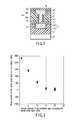
- FIG. 3is a graph showing computation results of stress exerted on a barrier metal layer of a via sidewall, which are obtained by simulation.
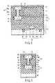
- FIG. 5is a cross-sectional view showing part of the semiconductor device according to the first embodiment of the present invention.
- FIG. 7is a cross-sectional view showing an example of a wiring structure of a semiconductor device according to a third embodiment of the present invention.
- FIGS. 8A to 8 Eare cross-sectional views of steps of manufacturing the wiring structure of the semiconductor device according to the third embodiment of the present invention.
- FIG. 9is a cross-sectional view showing another example of the wiring structure of the semiconductor device according to the third embodiment of the present invention.
- FIG. 10is a cross-sectional view showing still another example of the wiring structure of the semiconductor device according to the third embodiment of the present invention.
- FIGS. 11A to 11 Eare cross-sectional views of steps of manufacturing the wiring structure of the semiconductor device shown in FIG. 10.
- FIG. 12is a cross-sectional view showing yet another example of the wiring structure of the semiconductor device according to the third embodiment of the present invention.
- FIGS. 13A to 13 Eare cross-sectional views of steps of manufacturing the wiring structure of the semiconductor device shown in FIG. 12.
- FIG. 14is a cross-sectional view showing yet another example of the wiring structure of the semiconductor device according to the third embodiment of the present invention.
- FIG. 2is a cross-sectional view of a wiring structure of a semiconductor device according to a first embodiment of the present invention.
- an insulation layer 11is formed on a semiconductor substrate 24 , and a lower wiring layer 12 is buried in the insulation layer 11 with a barrier metal layer 18 interposed therebetween.
- the insulation layer 11has a laminated structure of a low dielectric constant insulation film 11 a as will be described below and a high strength insulation film 11 b having a high fracture strength and serving as a cap layer, such as a silicon oxide film, a silicon nitride film and a silicon carbide film.
- the insulation layer 11can be formed of a single layer.
- a silicon nitride film 13(whose relative dielectric constant is 7.0 and Young's modulus is 100 GPa) acting as an etching stopper layer is formed on the insulation layer 11 and a low dielectric constant insulation film 14 is formed on the silicon nitride film 13 .
- the film 14can be made of, for example, SiO(CH 3 ) x (whose relative dielectric constant is 2.5 and Young's modulus is 10 GPa or lower).
- the film 14can also be made of hydrogen silsesquioxane, a carbon-contained SiO 2 film (SiOC), a porous silica film, a polymer film, an (fluorine-doped) amorphous carbon film, or the like.
- the Young's modulus of these materialsis about 10 GPa or lower.
- An upper wiring layer 19 bis buried in the low dielectric constant insulation film 14 and connected to the lower wiring layer 12 through a plug 19 a.
- the upper wiring layer 19 b and plug 19 ahave a barrier metal layer 18 on their surfaces.
- the barrier metal layer 18can be made of Ta, Ti, Nb, an alloy containing the elements, a compound of the elements, or a laminated film of the elements.
- the conductive layer 19 such as the upper wiring layer 19 b and plug 19 acan be formed of Cu, Al, or an alloy containing these elements.
- a high Young's modulus insulation film 16whose Young's modulus is 15 GPa or higher is formed between the barrier metal layer 18 formed on the side of the plug 19 a and the low dielectric constant interlayer insulation film 14 .
- the insulation film 16can be formed of a silicon oxide (SiO) film (whose relative dielectric constant is 4.0 and Young's modulus is 60 GPa), a silicon nitride (SiN) film (whose relative dielectric constant is 7.0 and Young's modulus is 100 GPa), or the like.
- FIG. 3is a graph showing computation results of stress exerted on the barrier metal layer of a via sidewall, which are obtained by simulation. As is apparent from FIG. 3, the stress exerted on the barrier metal layer increases suddenly when the Young's modulus of the insulation layer contacting the barrier metal layer is lower than 15 GPa. The sudden increase in stress causes a crack to the barrier metal layer.
- the high Young's modulus insulation film 16is also formed on the low dielectric constant insulation film 14 and serves as a cap layer.
- a silicon nitride film 20is provided on the high Young's modulus insulation film 16 and upper wiring layer 19 b.
- FIG. 2A method for forming the wiring structure shown in FIG. 2 will be described with reference to FIGS. 4A to 4 E.
- a via hole 15is formed in the low dielectric constant insulation film 14 by RIE.
- the RIEcauses a damaged layer 21 to be formed on the surface of the insulation film 14 .
- the damaged layer 21 so formedis removed by wet etching using hydrofluoric acid. Then, a silicon oxide film serving as a high Young's modulus insulation film 16 is formed by plasma CVD on the entire surface of the low dielectric constant insulation film 14 in which the via hole 15 is formed, as shown in FIG. 4C.
- the silicon oxide filmhas a Young's modulus of 60 GPa and a thickness of 50 nm.
- a wiring groove 17is formed by RIE in a region including the via hole 15 of the low dielectric constant insulation film 14 and the high Young's modulus insulation film 16 .
- the high Young's modulus insulation film 16is removed from the bottom of the via hole 15 but remains on the low dielectric constant insulation film 14 .
- the remaining filmserves as a cap layer.
- the RIEcauses a damaged layer 21 to be formed on the surface of the insulation film 14 on the sidewall and bottom of the wiring groove 17 , which does not become a problem in particular.
- the silicon nitride film 13is removed from the bottom of the via hole 15 by RIE to expose the surface of the lower wiring layer 12 .
- one of Ta, Ti, Nb, TaN, TiN and NbN or a laminated film containing two or more of these elementsis deposited on the entire surface of the resultant structure at about 150° C. to form a barrier metal layer 18 . Furthermore, Cu acting as a plating seed is deposited and then Cu as a conductive material is deposited by plating to bury a conductive layer 19 into the via hole 15 and wiring groove 17 . After that, the resultant structure is annealed at about 400° C. in a forming gas.
- barrier metal layer 18 and conductive layer 19are removed by CMP from a region on the low dielectric constant insulation film 14 excluding the wiring groove 17 .
- a silicon nitride film 20is formed on the entire surface of the resultant structure by plasma CVD, thereby obtaining a wiring structure as shown in FIG. 2.
- the sidewall of the via holewhich is most likely to be cracked, is covered with the high Young's modulus insulation film 16 having a Young's modulus of 15 GPa or higher, as has been described above. Thermal stress is therefore prevented from being exerted on the barrier metal layer 18 . Since, moreover, the damaged layer is eliminated, the sidewall of the via hole includes no low fracture strength region.
- the high Young's modulus insulation film 16 formed on the sidewall of the via holehas a high fracture strength as described above. Consequently, the low dielectric constant insulation film 14 is not cracked even through the annealing step and its subsequent sintering step.
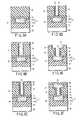
- FIGS. 6A to 6 Fare cross-sectional views of steps of forming a wiring structure of a semiconductor device according to a second embodiment of the present invention.
- a lower wiring layer 12 buried in an insulation film 11 , a silicon nitride film 13 acting as an etching stopper film, and a low dielectric constant insulation film 14are formed in sequence on a semiconductor substrate 24 by the same technique as that of the foregoing first embodiment.
- a via hole 15is formed in the insulation film 14 by RIE using a resist pattern 22 as an etching mask.
- the RIEcauses a damaged layer 21 to be formed on the surface of the insulation film 14 .
- a silicon nitride film 20is formed on the entire surface of the resultant structure, thereby obtaining a wiring structure as shown in FIG. 6F.
- FIG. 7is a cross-sectional view showing a wiring structure of a semiconductor device according to a third embodiment of the present invention.
- an insulation layer 11is provided on a semiconductor substrate 24 .
- a lower wiring layer 12is buried in the insulation layer 11 .
- the insulation layer 11has a laminated structure of a low dielectric constant insulation film 11 a and a high strength insulation film 11 b .
- a silicon nitride film 13(whose relative dielectric constant is 7.0 and Young's modulus is 100 GPa) acting as an etching stopper layer is formed on the insulation layer 11 and a low dielectric constant insulation film 14 is formed on the silicon nitride film 13 .
- the insulation film 14can be made of, for example, SiO(CH 3 ) x (whose relative dielectric constant is 2.5 and Young's modulus is 10 GPa or lower).
- the insulation film 14can also be made of oxide materials such as hydrogen silsesquioxane, carbon-contained SiO 2 (SiOC), and porous silica.
- An upper wiring layer 19 bis buried in the low dielectric constant insulation film 14 and connected to the lower wiring layer 12 through a plug 19 a .
- the upper wiring layer 19 b and plug 19 ahave a barrier metal layer 18 on their surfaces.
- a high Young's modulus insulation film 23 ′is formed at an interface between the insulation film 14 and barrier metal layer 18 .
- the insulation film 23 ′is a metal oxide layer having a Young's modulus of 15 GPa or higher.
- the metal oxide layeris an oxide containing at least one metal selected from the group consisting of Ta, Ti, Nb and Al.
- the metal oxide layercan be formed by sputtering at high temperature or annealing after a metal film is formed. Since such a metal oxide layer has a high Young's modulus of about 100 GPa to 200 GPa, it can prevent the stress exerted on the barrier metal layer from increasing if it is formed on the sidewall of the via hole. Since, moreover, the metal oxide layer so formed has a high fracture strength as the silicon oxide film and silicon nitride film do, even though a crack occurs in the barrier metal layer 18 , it can be prevented from progressing to the low dielectric constant insulation film 14 .
- the thickness of the high Young's modulus insulation film 23 ′range from 1 nm to 100 nm.
- a lower wiring layer 12 buried in an insulation film 11 , a silicon nitride film 13 acting as an etching stopper film, and a low dielectric constant insulation film 14are formed by the same technique as that of the foregoing first embodiment.
- a silicon oxide film 25 acting as a cap layeris formed on the insulation film 14 by plasma CVD.
- a via hole 15 connected to the lower wiring layer 12 and a wiring groove 17are formed by RIE in an insulation layer including the silicon nitride film 13 , low dielectric constant insulation film 14 , and silicon oxide film 25 .
- the RIEcauses a damaged layer 21 to be formed on the surface of the insulation film 14 .
- a high Young's modulus insulation film 23 ′is formed at the region of the damaged layer 21 as illustrated in FIG. 8C.
- the insulation film 23 ′is a metal oxide layer containing Ta, Ti, Nb or Al.
- a metal oxide layer containing Ta, Ti or Nbcan be formed by sputtering Ta, Ti or Nb at a temperature of about 300° C. to 450° C. in a vacuum. Due to the high temperature sputtering, such metal is diffused into the damaged layer 21 of the low dielectric constant insulation film 14 and reacts with the insulation film 14 to form a high Young's modulus insulation film 23 ′ that is made of a metal oxide layer.
- a metal oxide layer containing Alis formed by forming an Al film by sputtering or MOCVD and then annealing it at a temperature of about 100° C. to 450° C.
- the atmosphere of the sputtering and MOCVDis not limited, but they can be performed in a vacuum or a forming gas. Due to the annealing, Al is diffused into the damaged layer 21 of the low dielectric constant insulation film 14 and reacts with the insulation film 14 to form a high Young's modulus insulation film 23 ′ that is made of a metal oxide layer.
- Ta, Ti and Nbeach have Cu barrier properties. If, therefore, a metal oxide is formed while its thickness is controlled and a metal film is left on the surface of the metal oxide, it can be used as a barrier metal layer. Since Al has Cu barrier properties in an alumina state, a metal oxide layer itself can be used as a barrier layer. When all the deposited Al film is oxidized to form an alumina layer, Cu wiring can be buried without forming any additional barrier metal layer. This is very advantageous to a reduction in manufacturing steps. The Al film may remain on the surface of the metal oxide layer if the metal oxide layer has a required thickness.
- the sidewall of the via holewhich is most likely to be cracked, is covered with the high Young's modulus insulation film 23 ′ made of a metal oxide whose Young's modulus is 15 GPa or higher. Thermal stress exerted on the barrier metal layer 18 is therefore prevented from increasing. Since the high Young's modulus insulation film 23 ′ is formed by diffusion of metal in the damaged layer 21 whose fracture strength is low, the damaged layer 21 disappears and the insulation film 23 ′ having a high fracture strength contacts the barrier metal layer 18 . Consequently, the low dielectric constant insulation film 14 is not cracked even through the annealing step and its subsequent sintering step.
- FIG. 9This wiring structure can be formed by the same technique as described above and differs from the foregoing structures only in that no barrier metal layer is formed.
- a high Young's modulus insulation film 26that is made of a metal oxide (alumina) layer containing Al is formed in contact with the side of a plug 19 a.
- a damaged layer 21disappears from the sidewall of the via hole, which is most likely to be cracked, and the sidewall is covered with the high Young's modulus insulation film 26 made of an alumina layer having a high fracture strength and a Young's modulus of 15 GPa or higher. Consequently, the low dielectric constant insulation film 14 is not cracked even through the annealing step and its subsequent sintering step.
- FIG. 9The wiring structure shown in FIG. 9 can be modified as shown in FIG. 10.
- an upper wiring layer 49 bis buried and connected to the lower wiring layer 42 through a plug 49 a .
- a high Young's modulus insulation film 48 made of aluminais formed between the conductive material such as the upper wiring layer 49 b and the plug 49 a and the insulation film such as the low dielectric constant insulation film 46 , cap insulation film 47 and the low dielectric constant insulation film 44 .
- FIG. 10A method for forming the wiring structure shown in FIG. 10 will now be described with reference to FIGS. 11A to 11 E.
- a wiring layer 42 buried in an insulation film 41 , a stopper insulation film 43 made of a silicon carbonitride film, a low dielectric constant insulation film 44 made of a porous organosilicon oxide film, a mid-stopper layer 45 made of a silicon carbonitride film, and a low dielectric constant insulation film 46 made of a porous organosilicon oxide filmare formed in the order designated.
- An organosilicon oxide film 47 acting as a cap layeris formed on the low dielectric constant insulation film 46 .
- a via hole connected to the lower wiring layer 42 and a wiring grooveare formed in the insulation films by RIE using the stopper insulation film 43 and mid-stopper layer 45 as etching stoppers, respectively.
- a damaged layer(not shown) is formed on the surfaces of the low dielectric constant insulation films 44 and 46 .
- the mid-stopper layer 45is also removed from the bottom of the wiring groove.
- an Al film 50is formed on the entire surface of the resultant structure as shown in FIG. 11A by the same technique as that of the third embodiment.
- a high Young's modulus insulation film 48 made of an alumina layeris formed at an interface between the Al film 50 and each of the low dielectric constant insulation films 44 and 46 by annealing, as shown in FIG. 11B.
- the high Young's modulus insulation film 48is formed on the top surface and sides of the cap layer 47 since the cap layer 47 is made of organosilicon oxide.
- the wiring structurecan also be modified as shown in FIG. 12.
- the wiring structure shown in FIG. 12is the same as that shown in FIG. 10, except that a mid-stopper layer 45 made of a silicon carbonitride film is formed on the bottom of the upper wiring layer 49 b.
- FIG. 12A method for forming the wiring structure shown in FIG. 12 will now be described with reference to FIGS. 13A to 13 E.
- insulation layers 41 , 43 , 44 , 45 , 46 and 47are formed by the same technique as described in the case of FIG. 11A, except that the mid-stopper layer 45 is thickened, then a via hole and a wiring groove are formed by RIE. Since the mid-stopper layer 45 is thick, it is not completely eliminated but remains when the insulation film 43 is removed from the bottom of the via hole. After that, an Al film 50 is formed on the entire surface of the resultant structure by the same technique as described above, as shown in FIG. 13A.
- a high Young's modulus insulation film 48 made of an alumina layeris formed at an interface between the Al film 50 and each of the insulation films 44 and 46 by annealing, as shown in FIG. 13B.
- the high Young's modulus insulation film 48is formed on the top surface and sides of the cap insulation layer 47 since the layer 47 is made of organosilicon oxide.
- the mid-stopper layer 45 made of a silicon carbonitride filmis formed on the bottom of the wiring groove. Since the silicon carbide film has a dielectric constant that is lower than that of alumina, it is advantageous to a high-speed operation of an LSI.
- a semiconductor devicecapable of operating at high speed without causing any short circuit and a method for manufacturing the semiconductor device.
- the present inventionis very effective at forming a multilayer wiring structure using a low dielectric constant insulation film and its industrial significance is very great.
Landscapes
- Engineering & Computer Science (AREA)
- Physics & Mathematics (AREA)
- Condensed Matter Physics & Semiconductors (AREA)
- General Physics & Mathematics (AREA)
- Computer Hardware Design (AREA)
- Microelectronics & Electronic Packaging (AREA)
- Power Engineering (AREA)
- Manufacturing & Machinery (AREA)
- Internal Circuitry In Semiconductor Integrated Circuit Devices (AREA)
Abstract
Description
- This application is based upon and claims the benefit of priority from the prior Japanese Patent Application No. 2001-395237, filed Dec. 26, 2001, the entire contents of which are incorporated herein by reference.[0001]
- 1. Field of the Invention[0002]
- The present invention relates to a semiconductor device having a multilayer wiring structure using a low-dielectric-constant interlayer insulation film, and a method for manufacturing the semiconductor device.[0003]
- 2. Description of the Related Art[0004]
- Materials having a relative dielectric constant of 3 or lower have recently been used for low dielectric constant interlayer insulation films in order to increase the operation speed of an LSI. The Young's modulus of such a low dielectric constant insulation film is generally about 10 GPa or lower. The coefficient of linear expansion of Cu used as wiring materials is as large as about 16 ppm. However, when a Cu wiring layer is formed, a barrier metal layer comprising refractory metal such as Ta and Ti and a compound thereof, is formed between the Cu wiring layer and an interlayer insulation film. The coefficient of linear expansion of barrier metal is not larger than 10 ppm and smaller than that of Cu. Thus, a great thermal stress is exerted on the barrier metal layer due to a difference in coefficient of linear expansion between barrier metal and Cu wiring layer during a high-temperature process such as annealing and sintering.[0005]
- If the Young's modulus of the low-dielectric-constant insulation film is sufficiently large, the stress applied to the barrier metal layer can be decreased by suppressing the thermal expansion of Cu. However, the Young's modulus of the low dielectric constant insulation film is about 10 GPa or lower, as described above. Therefore, the thermal stress applied to the barrier metal layer becomes great and causes a crack to the low dielectric constant insulation film.[0006]
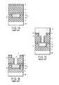
- It is around a via hole that such a crack is most likely to occur. Referring to FIGS. 1A to[0007]1C, a problem of the crack in the wiring structure of a prior art semiconductor device will be described.
- As shown in FIG. 1A, an[0008]
insulation film 1 having a laminated structure of a low dielectricconstant insulation film 1aand a high fracture strengthcap insulation film 1bis formed on asemiconductor substrate 24 and alower wiring layer 2 is buried in theinsulation film 1 with abarrier metal layer 9 interposed therebetween. An etchingstopper insulation film 3, a low dielectricconstant insulation film 4, and a high fracture strengthcap insulation film 5 are formed in sequence. As shown in FIG. 1B, a viahole 6 connected to thelower wiring layer 2 and awiring groove 7 are formed in theinsulation films constant insulation film 4 is damaged by the RIE to form a low fracture strength damagedlayer 8. - After that, as shown in FIG. 1C, barrier metal is deposited in the via[0009]
hole 6 and on the entire surface of thewiring groove 7 by sputtering. Thebarrier metal layer 9 formed on the sidewalls of the viahole 6 is thinner than that formed on the sidewalls and bottom of thewiring groove 7 and the bottom of the viahole 6. Then,conductive materials 10 such as Cu are deposited and the resultant structure is annealed at high temperature. During the high temperature annealing, a tensile stress is exerted on thebarrier metal layer 9 due to a difference in coefficient of linear expansion between them. - Since, in particular, the[0010]
barrier metal layer 9 formed on the sidewalls of the viahole 6 is thin, it is likely to be cracked by the tensile stress. The fracture strength of the damagedlayer 8 that is formed in contact with thebarrier metal layer 9 is low and thus the crack caused in thebarrier metal layer 9 might come into the low dielectricconstant insulation film 4 through the damagedlayer 8. Consequently, theconductive materials 10 such as Cu, which are compressed at high temperature, are protruded from the crack and a short circuit will occur. - A semiconductor device according to one aspect of the present invention comprises:[0011]
- a semiconductor substrate on which an element is formed;[0012]
- a low dielectric constant insulation film formed over the semiconductor substrate and having a relative dielectric constant of 3 or lower;[0013]
- a plug and a wiring layer buried in the low dielectric constant insulation film; and[0014]
- a high Young's modulus insulation film having a Young's modulus of 15 GPa or higher and formed in contact with a side of the plug between the low dielectric constant insulation film and the plug.[0015]
- A method for manufacturing a semiconductor device according to one aspect of the present invention, comprises:[0016]
- forming a lower wiring layer over a semiconductor substrate with an insulation film interposed therebetween, an element being formed on the semiconductor substrate;[0017]
- forming a low dielectric constant insulation film having a relative dielectric constant of 3 or lower on the lower wiring layer;[0018]
- forming a via hole in the low dielectric constant insulation film;[0019]
- forming a high Young's modulus insulation film having a Young's modulus of 15 GPa or higher on a sidewall of the via hole;[0020]
- forming a wiring groove in the low dielectric constant insulation film with the via hole on the sidewall of which the high Young's modulus insulation film is formed;[0021]
- depositing a barrier metal and a conductive material in sequence on a surface of the low dielectric constant insulation film in which the via hole and the wiring groove are formed, such that the barrier metal and the conductive material are electrically connected to the lower wiring layer; and[0022]
- removing the barrier metal and the conductive material deposited outside the via hole and the wiring groove to form a plug and an upper wiring layer each having a barrier metal layer on a surface thereof in the via hole and the wiring groove, respectively.[0023]
- A method for manufacturing a semiconductor device according to one aspect of the present invention, comprises:[0024]
- forming a lower wiring layer over a semiconductor substrate with an insulation film interposed therebetween, an element being formed on the semiconductor substrate;[0025]
- forming a low dielectric constant insulation film having a relative dielectric constant of 3 or lower on the lower wiring layer;[0026]
- forming a via hole and a wiring groove in the low dielectric constant insulation film;[0027]
- forming a high Young's modulus insulation film on a surface of the low dielectric constant insulation film in which the via hole and the wiring groove are formed, the high Young's modulus insulation film having a Young's modulus of 15 GPa or higher and including a metal oxide containing at least one metal selected from a group consisting of Ta, Ti, Nb and Al;[0028]
- depositing a conductive material on a surface of the low dielectric constant insulation film in which the high Young's modulus insulation film is formed, such that the conductive material is electrically connected to the lower wiring layer; and[0029]
- removing the conductive material deposited outside the via hole and the wiring groove to form a plug and an upper wiring layer in the via hole and the wiring groove, respectively.[0030]
- FIGS. 1A to[0031]1C are cross-sectional views of steps of manufacturing a wiring structure of a prior art semiconductor device.
- FIG. 2 is a cross-sectional view of a wiring structure of a semiconductor device according to a first embodiment of the present invention.[0032]
- FIG. 3 is a graph showing computation results of stress exerted on a barrier metal layer of a via sidewall, which are obtained by simulation.[0033]
- FIGS. 4A to[0034]4E are cross-sectional views of steps of manufacturing the wiring structure of the semiconductor device according to the first embodiment of the present invention.
- FIG. 5 is a cross-sectional view showing part of the semiconductor device according to the first embodiment of the present invention.[0035]
- FIGS. 6A to[0036]6F are cross-sectional views of steps of manufacturing a wiring structure of a semiconductor device according to a second embodiment of the present invention.
- FIG. 7 is a cross-sectional view showing an example of a wiring structure of a semiconductor device according to a third embodiment of the present invention.[0037]
- FIGS. 8A to[0038]8E are cross-sectional views of steps of manufacturing the wiring structure of the semiconductor device according to the third embodiment of the present invention.
- FIG. 9 is a cross-sectional view showing another example of the wiring structure of the semiconductor device according to the third embodiment of the present invention.[0039]
- FIG. 10 is a cross-sectional view showing still another example of the wiring structure of the semiconductor device according to the third embodiment of the present invention.[0040]
- FIGS. 11A to[0041]11E are cross-sectional views of steps of manufacturing the wiring structure of the semiconductor device shown in FIG. 10.
- FIG. 12 is a cross-sectional view showing yet another example of the wiring structure of the semiconductor device according to the third embodiment of the present invention.[0042]
- FIGS. 13A to[0043]13E are cross-sectional views of steps of manufacturing the wiring structure of the semiconductor device shown in FIG. 12.
- FIG. 14 is a cross-sectional view showing yet another example of the wiring structure of the semiconductor device according to the third embodiment of the present invention.[0044]
- Embodiments of the present invention will now be described in detail with reference to the accompanying drawings.[0045]
- (First Embodiment)[0046]
- FIG. 2 is a cross-sectional view of a wiring structure of a semiconductor device according to a first embodiment of the present invention.[0047]
- In the semiconductor device shown in FIG. 2, an[0048]
insulation layer 11 is formed on asemiconductor substrate 24, and alower wiring layer 12 is buried in theinsulation layer 11 with abarrier metal layer 18 interposed therebetween. Theinsulation layer 11 has a laminated structure of a low dielectricconstant insulation film 11aas will be described below and a highstrength insulation film 11bhaving a high fracture strength and serving as a cap layer, such as a silicon oxide film, a silicon nitride film and a silicon carbide film. However, theinsulation layer 11 can be formed of a single layer. A silicon nitride film13 (whose relative dielectric constant is 7.0 and Young's modulus is 100 GPa) acting as an etching stopper layer is formed on theinsulation layer 11 and a low dielectricconstant insulation film 14 is formed on thesilicon nitride film 13. Thefilm 14 can be made of, for example, SiO(CH3)x(whose relative dielectric constant is 2.5 and Young's modulus is 10 GPa or lower). Thefilm 14 can also be made of hydrogen silsesquioxane, a carbon-contained SiO2film (SiOC), a porous silica film, a polymer film, an (fluorine-doped) amorphous carbon film, or the like. The Young's modulus of these materials is about 10 GPa or lower. - An[0049]
upper wiring layer 19bis buried in the low dielectricconstant insulation film 14 and connected to thelower wiring layer 12 through aplug 19a.Theupper wiring layer 19band plug19ahave abarrier metal layer 18 on their surfaces. Thebarrier metal layer 18 can be made of Ta, Ti, Nb, an alloy containing the elements, a compound of the elements, or a laminated film of the elements. Theconductive layer 19 such as theupper wiring layer 19band plug19acan be formed of Cu, Al, or an alloy containing these elements. - A high Young's[0050]
modulus insulation film 16 whose Young's modulus is 15 GPa or higher is formed between thebarrier metal layer 18 formed on the side of theplug 19aand the low dielectric constantinterlayer insulation film 14. Theinsulation film 16 can be formed of a silicon oxide (SiO) film (whose relative dielectric constant is 4.0 and Young's modulus is 60 GPa), a silicon nitride (SiN) film (whose relative dielectric constant is 7.0 and Young's modulus is 100 GPa), or the like. Thefilm 16 can also be formed of a silicon oxynitride (SiON) film (whose relative dielectric constant is 4.0 to 5.0 and Young's modulus is 80 GPa to 100 GPa), a silicon carbonitride (SiCN) film (whose relative dielectric constant is 4.0 to 5.0 and Young's modulus is 100 GPa). - FIG. 3 is a graph showing computation results of stress exerted on the barrier metal layer of a via sidewall, which are obtained by simulation. As is apparent from FIG. 3, the stress exerted on the barrier metal layer increases suddenly when the Young's modulus of the insulation layer contacting the barrier metal layer is lower than 15 GPa. The sudden increase in stress causes a crack to the barrier metal layer.[0051]
- In the first embodiment, since the high Young's modulus insulation film having a Young's modulus of 15 GPa or higher is formed on the sidewall of the via hole, the stress on the barrier metal layer can be prevented from increasing. Since, moreover, the high Young's modulus insulation film has a high fracture strength, even though a crack occurs in the barrier metal layer, it is prevented from progressing to the low dielectric constant insulation film.[0052]
- The effect of the high Young's modulus insulation film formed on the sidewall of the via hole can be produced if its thickness is at least 1 nm. If, however, the high Young's modulus insulation film is formed excessively thick, there is a fear that the dielectric constant of the interlayer insulation film will undesirably increase. It is thus desirable that the upper limit of the thickness be at most 100 nm.[0053]
- In the wiring structure shown in FIG. 2, the high Young's[0054]
modulus insulation film 16 is also formed on the low dielectricconstant insulation film 14 and serves as a cap layer. Asilicon nitride film 20 is provided on the high Young'smodulus insulation film 16 andupper wiring layer 19b. - A method for forming the wiring structure shown in FIG. 2 will be described with reference to FIGS. 4A to[0055]4E.
- Referring first to FIG. 4A, a low dielectric[0056]
constant insulation film 11aand a highstrength insulation layer 11bare deposited in sequence on asemiconductor substrate 24 to form aninsulation film 11, and alower wiring layer 12 having abarrier metal layer 18 on its surface is buried in theinsulation film 11. Further, asilicon nitride film 13 serving as an etching stopper film is formed by plasma CVD and a low dielectricconstant insulation film 14 is formed by spin coating using, e.g., SiO(CH3)x. - As shown in FIG. 4B, a via[0057]
hole 15 is formed in the low dielectricconstant insulation film 14 by RIE. The RIE causes a damagedlayer 21 to be formed on the surface of theinsulation film 14. - The damaged[0058]
layer 21 so formed is removed by wet etching using hydrofluoric acid. Then, a silicon oxide film serving as a high Young'smodulus insulation film 16 is formed by plasma CVD on the entire surface of the low dielectricconstant insulation film 14 in which the viahole 15 is formed, as shown in FIG. 4C. The silicon oxide film has a Young's modulus of 60 GPa and a thickness of 50 nm. - As illustrated in FIG. 4D, a[0059]
wiring groove 17 is formed by RIE in a region including the viahole 15 of the low dielectricconstant insulation film 14 and the high Young'smodulus insulation film 16. By forming thewiring groove 17, the high Young'smodulus insulation film 16 is removed from the bottom of the viahole 15 but remains on the low dielectricconstant insulation film 14. The remaining film serves as a cap layer. The RIE causes a damagedlayer 21 to be formed on the surface of theinsulation film 14 on the sidewall and bottom of thewiring groove 17, which does not become a problem in particular. After that, thesilicon nitride film 13 is removed from the bottom of the viahole 15 by RIE to expose the surface of thelower wiring layer 12. - As depicted in FIG. 4E, one of Ta, Ti, Nb, TaN, TiN and NbN or a laminated film containing two or more of these elements is deposited on the entire surface of the resultant structure at about 150° C. to form a[0060]
barrier metal layer 18. Furthermore, Cu acting as a plating seed is deposited and then Cu as a conductive material is deposited by plating to bury aconductive layer 19 into the viahole 15 andwiring groove 17. After that, the resultant structure is annealed at about 400° C. in a forming gas. - Finally, the[0061]
barrier metal layer 18 andconductive layer 19 are removed by CMP from a region on the low dielectricconstant insulation film 14 excluding thewiring groove 17. Asilicon nitride film 20 is formed on the entire surface of the resultant structure by plasma CVD, thereby obtaining a wiring structure as shown in FIG. 2. - FIG. 5 shows part of a semiconductor device having a wiring structure as described above. In this semiconductor device, source and drain[0062]
regions semiconductor substrate 24 that is interposed between element isolatinginsulation films 32. Agate insulation film 33 is formed between the source and drainregions gate electrode 34 is formed on thegate insulation film 33. The source and drainregions insulation films 32,gate insulation film 33, andgate electrode 34 make up anactive element 30 in thesemiconductor substrate 24. The same wiring structure as shown in FIG. 2 is provided on thissemiconductor substrate 24. - In the wiring structure of the semiconductor device shown in FIG. 5, the sidewall of the via hole, which is most likely to be cracked, is covered with the high Young's[0063]
modulus insulation film 16 having a Young's modulus of 15 GPa or higher, as has been described above. Thermal stress is therefore prevented from being exerted on thebarrier metal layer 18. Since, moreover, the damaged layer is eliminated, the sidewall of the via hole includes no low fracture strength region. The high Young'smodulus insulation film 16 formed on the sidewall of the via hole has a high fracture strength as described above. Consequently, the low dielectricconstant insulation film 14 is not cracked even through the annealing step and its subsequent sintering step. - (Second Embodiment)[0064]
- FIGS. 6A to[0065]6F are cross-sectional views of steps of forming a wiring structure of a semiconductor device according to a second embodiment of the present invention.
- As illustrated in FIG. 6A, a[0066]
lower wiring layer 12 buried in aninsulation film 11, asilicon nitride film 13 acting as an etching stopper film, and a low dielectricconstant insulation film 14 are formed in sequence on asemiconductor substrate 24 by the same technique as that of the foregoing first embodiment. - As depicted in FIG. 6B, a via[0067]
hole 15 is formed in theinsulation film 14 by RIE using a resistpattern 22 as an etching mask. The RIE causes a damagedlayer 21 to be formed on the surface of theinsulation film 14. - Before the resist[0068]
pattern 22 is removed, as shown in FIG. 6C, a high Young'smodulus insulation film 16 having a Young's modulus of 15 GPa or higher is formed on the entire surface of the resultant structure by plasma CVD. The high Young'smodulus insulation film 16 can be formed of a silicon oxide film or a silicon nitride film, as has been described above. Before theinsulation film 16 is formed, the damagedlayer 21 can be removed from the surface of the low dielectricconstant insulation film 14 by the same technique as that of the first embodiment. - The resist[0069]
pattern 22 and the high Young'smodulus insulation film 16 formed thereon are removed by lift-off as shown in FIG. 6D. After that, awiring groove 17 is formed in the low dielectricconstant insulation film 14 by RIE as shown in FIG. 6E. The RIE causes a damagedlayer 21 to be formed on theinsulation film 14 on the sidewall and bottom of thewiring groove 17, which does not become a problem. After that, thesilicon nitride film 13 is removed from the bottom of the viahole 15 by RIE to expose the surface of thelower wiring layer 12. - After the[0070]
barrier metal layer 18 andconductive layer 19 are buried in the viahole 15 andwiring groove 17 by the same technique as that of the first embodiment, asilicon nitride film 20 is formed on the entire surface of the resultant structure, thereby obtaining a wiring structure as shown in FIG. 6F. - In the semiconductor device having the above wiring structure, the sidewall of the via hole, which is most likely to be cracked, is covered with the high Young's[0071]
modulus insulation film 16 having a Young's modulus of 15 GPa or higher. Thermal stress is therefore prevented from being exerted on thebarrier metal layer 18. Since, moreover, theinsulation film 16 has high fracture strength, the low dielectricconstant insulation film 14 is not cracked even through the annealing step and its subsequent sintering step. - (Third Embodiment)[0072]
- FIG. 7 is a cross-sectional view showing a wiring structure of a semiconductor device according to a third embodiment of the present invention.[0073]
- In the wiring structure shown in FIG. 7, an[0074]
insulation layer 11 is provided on asemiconductor substrate 24. Alower wiring layer 12 is buried in theinsulation layer 11. Theinsulation layer 11 has a laminated structure of a low dielectricconstant insulation film 11aand a highstrength insulation film 11b. A silicon nitride film13 (whose relative dielectric constant is 7.0 and Young's modulus is 100 GPa) acting as an etching stopper layer is formed on theinsulation layer 11 and a low dielectricconstant insulation film 14 is formed on thesilicon nitride film 13. Theinsulation film 14 can be made of, for example, SiO(CH3)x(whose relative dielectric constant is 2.5 and Young's modulus is 10 GPa or lower). Theinsulation film 14 can also be made of oxide materials such as hydrogen silsesquioxane, carbon-contained SiO2(SiOC), and porous silica. - An[0075]
upper wiring layer 19bis buried in the low dielectricconstant insulation film 14 and connected to thelower wiring layer 12 through aplug 19a. Theupper wiring layer 19band plug19ahave abarrier metal layer 18 on their surfaces. A high Young'smodulus insulation film 23′ is formed at an interface between theinsulation film 14 andbarrier metal layer 18. Theinsulation film 23′ is a metal oxide layer having a Young's modulus of 15 GPa or higher. - The metal oxide layer is an oxide containing at least one metal selected from the group consisting of Ta, Ti, Nb and Al. As will be described below, the metal oxide layer can be formed by sputtering at high temperature or annealing after a metal film is formed. Since such a metal oxide layer has a high Young's modulus of about 100 GPa to 200 GPa, it can prevent the stress exerted on the barrier metal layer from increasing if it is formed on the sidewall of the via hole. Since, moreover, the metal oxide layer so formed has a high fracture strength as the silicon oxide film and silicon nitride film do, even though a crack occurs in the[0076]
barrier metal layer 18, it can be prevented from progressing to the low dielectricconstant insulation film 14. - For the reasons described above, it is desirable that the thickness of the high Young's[0077]
modulus insulation film 23′ range from 1 nm to 100 nm. - In the wiring structure shown in FIG. 7, a[0078]
silicon oxide film 25 is formed on the low dielectricconstant insulation film 14 and asilicon nitride film 20 is formed on thesilicon oxide film 25. - A method for forming the wiring structure shown in FIG. 7 will now be described with reference to FIGS. 8A to[0079]8E.
- As illustrated in FIG. 8A, a[0080]
lower wiring layer 12 buried in aninsulation film 11, asilicon nitride film 13 acting as an etching stopper film, and a low dielectricconstant insulation film 14 are formed by the same technique as that of the foregoing first embodiment. Asilicon oxide film 25 acting as a cap layer is formed on theinsulation film 14 by plasma CVD. - As depicted in FIG. 8B, a via[0081]
hole 15 connected to thelower wiring layer 12 and awiring groove 17 are formed by RIE in an insulation layer including thesilicon nitride film 13, low dielectricconstant insulation film 14, andsilicon oxide film 25. The RIE causes a damagedlayer 21 to be formed on the surface of theinsulation film 14. - A high Young's[0082]
modulus insulation film 23′ is formed at the region of the damagedlayer 21 as illustrated in FIG. 8C. Theinsulation film 23′ is a metal oxide layer containing Ta, Ti, Nb or Al. A metal oxide layer containing Ta, Ti or Nb can be formed by sputtering Ta, Ti or Nb at a temperature of about 300° C. to 450° C. in a vacuum. Due to the high temperature sputtering, such metal is diffused into the damagedlayer 21 of the low dielectricconstant insulation film 14 and reacts with theinsulation film 14 to form a high Young'smodulus insulation film 23′ that is made of a metal oxide layer. On the other hand, a metal oxide layer containing Al is formed by forming an Al film by sputtering or MOCVD and then annealing it at a temperature of about 100° C. to 450° C. The atmosphere of the sputtering and MOCVD is not limited, but they can be performed in a vacuum or a forming gas. Due to the annealing, Al is diffused into the damagedlayer 21 of the low dielectricconstant insulation film 14 and reacts with theinsulation film 14 to form a high Young'smodulus insulation film 23′ that is made of a metal oxide layer. - The fact that the high Young's[0083]
modulus insulation film 23′ is formed on the surface of the low dielectricconstant insulation film 14 means that the damagedlayer 21 has disappeared. In either case, the above metal does not react with the bottom of the viahole 15 or the surface of thesilicon oxide film 25, which corresponds to a region other than the low dielectricconstant insulation film 14; therefore, ametal film 23 is formed as shown in FIG. 8C. - Ta, Ti and Nb each have Cu barrier properties. If, therefore, a metal oxide is formed while its thickness is controlled and a metal film is left on the surface of the metal oxide, it can be used as a barrier metal layer. Since Al has Cu barrier properties in an alumina state, a metal oxide layer itself can be used as a barrier layer. When all the deposited Al film is oxidized to form an alumina layer, Cu wiring can be buried without forming any additional barrier metal layer. This is very advantageous to a reduction in manufacturing steps. The Al film may remain on the surface of the metal oxide layer if the metal oxide layer has a required thickness.[0084]
- A[0085]
barrier metal layer 18, which is to be formed as required, and aconductive layer 19 are buried in the viahole 15 andwiring groove 17 by the same technique as that of the first embodiment. After that, the resultant structure is annealed in a forming gas, thereby obtaining a structure as shown in FIG. 8D. - Finally, the[0086]
barrier metal layer 18,conductive layer 19, andunreacted metal film 23, which are deposited on a region of thesilicon oxide film 25 excluding thewiring groove 17, are removed by CMP, and asilicon nitride film 20 is formed on the entire surface of the resultant structure by plasma CVD, thereby forming a wiring structure as shown in FIG. 8E. - In the semiconductor device having the foregoing wiring structure, the sidewall of the via hole, which is most likely to be cracked, is covered with the high Young's[0087]
modulus insulation film 23′ made of a metal oxide whose Young's modulus is 15 GPa or higher. Thermal stress exerted on thebarrier metal layer 18 is therefore prevented from increasing. Since the high Young'smodulus insulation film 23′ is formed by diffusion of metal in the damagedlayer 21 whose fracture strength is low, the damagedlayer 21 disappears and theinsulation film 23′ having a high fracture strength contacts thebarrier metal layer 18. Consequently, the low dielectricconstant insulation film 14 is not cracked even through the annealing step and its subsequent sintering step. - As has been described above, no additional barrier metal layers need to be formed if an Al film is deposited and completely oxidized to form an alumina layer when a high Young's[0088]
modulus insulation film 23′ is formed as shown in FIG. 8C. In other words, a high Young's modulus insulation film serving as a barrier layer can be formed by a single step. The wiring structure in this case is shown in FIG. 9. This wiring structure can be formed by the same technique as described above and differs from the foregoing structures only in that no barrier metal layer is formed. In the structure shown in FIG. 9, a high Young'smodulus insulation film 26 that is made of a metal oxide (alumina) layer containing Al is formed in contact with the side of aplug 19a. - In the semiconductor device having the wiring structure so obtained, a damaged[0089]
layer 21 disappears from the sidewall of the via hole, which is most likely to be cracked, and the sidewall is covered with the high Young'smodulus insulation film 26 made of an alumina layer having a high fracture strength and a Young's modulus of 15 GPa or higher. Consequently, the low dielectricconstant insulation film 14 is not cracked even through the annealing step and its subsequent sintering step. - The wiring structure shown in FIG. 9 can be modified as shown in FIG. 10.[0090]
- In the wiring structure depicted in FIG. 10, an[0091]
insulation layer 41 in which alower wiring layer 42 is buried is provided on asemiconductor substrate 24. Theinsulation film 41 can have a laminated structure of a low dielectric constant insulation film and a high strength insulation film. Thelower wiring layer 42 can have a barrier metal layer on its surface; otherwise, the surface of theinsulation layer 41 that contacts thelower wiring layer 42 can serve as an alumina layer. - A[0092]
stopper insulation film 43 made of a silicon carbonitride film, a low dielectricconstant insulation film 44 made of a porous organosilicon oxide film, amid-stopper layer 45 made of a silicon carbonitride film, a low dielectricconstant insulation film 46 made of a porous organosilicon oxide film, and acap insulation film 47 made of an organosilicon oxide film are formed on theinsulation layer 41 in the order designated. - In this laminated structure, an[0093]
upper wiring layer 49bis buried and connected to thelower wiring layer 42 through aplug 49a. A high Young'smodulus insulation film 48 made of alumina is formed between the conductive material such as theupper wiring layer 49band theplug 49aand the insulation film such as the low dielectricconstant insulation film 46,cap insulation film 47 and the low dielectricconstant insulation film 44. - A method for forming the wiring structure shown in FIG. 10 will now be described with reference to FIGS. 11A to[0094]11E.
- A[0095]
wiring layer 42 buried in aninsulation film 41, astopper insulation film 43 made of a silicon carbonitride film, a low dielectricconstant insulation film 44 made of a porous organosilicon oxide film, amid-stopper layer 45 made of a silicon carbonitride film, and a low dielectricconstant insulation film 46 made of a porous organosilicon oxide film are formed in the order designated. Anorganosilicon oxide film 47 acting as a cap layer is formed on the low dielectricconstant insulation film 46. - Then, a via hole connected to the[0096]
lower wiring layer 42 and a wiring groove are formed in the insulation films by RIE using thestopper insulation film 43 andmid-stopper layer 45 as etching stoppers, respectively. As has been described above, a damaged layer (not shown) is formed on the surfaces of the low dielectricconstant insulation films stopper insulation film 43 is removed from the bottom of the via hole, themid-stopper layer 45 is also removed from the bottom of the wiring groove. After that, anAl film 50 is formed on the entire surface of the resultant structure as shown in FIG. 11A by the same technique as that of the third embodiment. - After that, a high Young's[0097]
modulus insulation film 48 made of an alumina layer is formed at an interface between theAl film 50 and each of the low dielectricconstant insulation films modulus insulation film 48 is formed on the top surface and sides of thecap layer 47 since thecap layer 47 is made of organosilicon oxide. - Then, unreacted aluminum (Al) is removed by wet etching to expose the high Young's[0098]
modulus insulation film 48 as illustrated in FIG. 11C. The sidewalls of the wiring groove and via hole have regions at which the stopper layers43 and45 are exposed, and these regions have Cu barrier properties. - After that, a Cu seed film (not shown) is formed on the entire surface of the resultant structure and, as shown in FIG. 11D, a[0099]
conductive layer 49 is buried in the Cu seed film by Cu electrolytic plating. Theconductive layer 49 deposited on the region other than the groove is eliminated by CMP as shown in FIG. 11E. Finally, the high Young'smodulus insulation film 48 is removed from the top surface of thecap layer 47 by CMP, thereby obtaining the wiring structure as shown in FIG. 10. - In the wiring structure shown in FIG. 10, the high Young's[0100]
modulus insulation film 48 is formed on the bottom of the wiring groove and thus the adhesion between theupper wiring layer 49band theinterlayer insulation film 44 is improved. Comparing with the wiring structure shown in FIG. 9, no Al film is formed on the bottom of the via hole and thus the following advantage is obtained. The resistance of an interface between thelower wiring layer 42 and the via plug49adecreases and the conductive materials of the upper and lower wiring layers are not separated by different materials, with the result that electromigration resistance and stress void resistance are improved. - The wiring structure can also be modified as shown in FIG. 12.[0101]
- The wiring structure shown in FIG. 12 is the same as that shown in FIG. 10, except that a[0102]
mid-stopper layer 45 made of a silicon carbonitride film is formed on the bottom of theupper wiring layer 49b. - A method for forming the wiring structure shown in FIG. 12 will now be described with reference to FIGS. 13A to[0103]13E.
- In the first step, insulation layers[0104]41,43,44,45,46 and47 are formed by the same technique as described in the case of FIG. 11A, except that the
mid-stopper layer 45 is thickened, then a via hole and a wiring groove are formed by RIE. Since themid-stopper layer 45 is thick, it is not completely eliminated but remains when theinsulation film 43 is removed from the bottom of the via hole. After that, anAl film 50 is formed on the entire surface of the resultant structure by the same technique as described above, as shown in FIG. 13A. - After that, a high Young's[0105]
modulus insulation film 48 made of an alumina layer is formed at an interface between theAl film 50 and each of theinsulation films modulus insulation film 48 is formed on the top surface and sides of thecap insulation layer 47 since thelayer 47 is made of organosilicon oxide. - Then, unreacted aluminum (Al) is removed by wet etching to expose the high Young's[0106]
modulus insulation film 48 as illustrated in FIG. 13C. Moreover, aconductive layer 49 is formed by the same technique as described above as shown in FIG. 13D and removed from the region other than the groove as shown in FIG. 13E. Finally, the high Young'smodulus insulation film 48 is removed from the top surface of theinsulation layer 47 to obtain the wiring structure shown in FIG. 12. - In the wiring structure shown in FIG. 12, the[0107]
mid-stopper layer 45 made of a silicon carbonitride film is formed on the bottom of the wiring groove. Since the silicon carbide film has a dielectric constant that is lower than that of alumina, it is advantageous to a high-speed operation of an LSI. - The wiring structure can also be modified as shown in FIG. 14.[0108]
- The wiring structure shown in FIG. 14 is the same as that shown in FIG. 10, except that low dielectric[0109]
constant insulation films modulus insulation film 54 made of aluminum carbide is formed at an interface between a Cuconductive layer 49 and each of theinsulation films modulus insulation film 54 made of aluminum carbide. - Like alumina, the aluminum carbide has a Young's modulus of 15 GPa or higher and Cu barrier properties. It can therefore be used as a barrier layer of Cu wiring.[0110]
- As has been described in detail, according to an aspect of the present invention, there is provided a semiconductor device capable of operating at high speed without causing any short circuit and a method for manufacturing the semiconductor device.[0111]
- The present invention is very effective at forming a multilayer wiring structure using a low dielectric constant insulation film and its industrial significance is very great.[0112]
Claims (20)
Applications Claiming Priority (2)
| Application Number | Priority Date | Filing Date | Title |
|---|---|---|---|
| JP2001395237AJP3648480B2 (en) | 2001-12-26 | 2001-12-26 | Semiconductor device and manufacturing method thereof |
| JP2001-395237 | 2001-12-26 |
Publications (2)
| Publication Number | Publication Date |
|---|---|
| US20030116854A1true US20030116854A1 (en) | 2003-06-26 |
| US6975033B2 US6975033B2 (en) | 2005-12-13 |
Family
ID=19188950
Family Applications (1)
| Application Number | Title | Priority Date | Filing Date |
|---|---|---|---|
| US10/247,378Expired - LifetimeUS6975033B2 (en) | 2001-12-26 | 2002-09-20 | Semiconductor device and method for manufacturing the same |
Country Status (6)
| Country | Link |
|---|---|
| US (1) | US6975033B2 (en) |
| EP (1) | EP1324383A3 (en) |
| JP (1) | JP3648480B2 (en) |
| KR (1) | KR20030055135A (en) |
| CN (1) | CN1293622C (en) |
| TW (1) | TW587274B (en) |
Cited By (29)
| Publication number | Priority date | Publication date | Assignee | Title |
|---|---|---|---|---|
| US20040166676A1 (en)* | 2002-09-12 | 2004-08-26 | Tetsunori Kaji | Method and apparatus for forming damascene structure, and damascene structure |
| US20040251550A1 (en)* | 2003-06-10 | 2004-12-16 | Takashi Yoda | Semiconductor device and method of manufacturing the same |
| US20050238853A1 (en)* | 2004-04-23 | 2005-10-27 | Samsung Electronics Co., Ltd. | Bonding structure for flat panel display, method of forming the same, and flat panel display including bonding structure |
| US20060103025A1 (en)* | 2004-11-15 | 2006-05-18 | Renesas Technology Corp. | Semiconductor device including sealing ring |
| US20060214305A1 (en)* | 2005-01-21 | 2006-09-28 | Atsuko Sakata | Semiconductor device having oxidized metal film and manufacture method of the same |
| US20060223306A1 (en)* | 2003-08-15 | 2006-10-05 | Kohei Kawamura | Method for forming film, method for manufacturing semiconductor device, semiconductor device and substrate treatment system |
| US7119442B2 (en) | 2004-03-11 | 2006-10-10 | Kabushiki Kaisha Toshiba | Semiconductor device |
| US20070108616A1 (en)* | 2004-06-03 | 2007-05-17 | Hideo Nakagawa | Semiconductor device and method for fabricating the same |
| US20070202676A1 (en)* | 2006-02-24 | 2007-08-30 | Taiwan Semiconductor Manufacturing Company, Ltd. | Integration scheme for cu/low-k interconnects |
| US20070209930A1 (en)* | 2006-03-09 | 2007-09-13 | Applied Materials, Inc. | Apparatus for fabricating a high dielectric constant transistor gate using a low energy plasma system |
| US20080003766A1 (en)* | 2006-06-29 | 2008-01-03 | Hynix Semiconductor Inc. | Method for manufacturing semiconductor device free from layer-lifting between insulating layers |
| US20080012138A1 (en)* | 2006-07-17 | 2008-01-17 | Taiwan Semiconductor Manufacturing Company, Ltd. | One-time-programmable anti-fuse formed using damascene process |
| US20080122121A1 (en)* | 2006-11-24 | 2008-05-29 | Fujitsu Limited | Semiconductor device having a interlayer insulation film with low dielectric constant and high mechanical strength |
| US20090142860A1 (en)* | 2007-11-29 | 2009-06-04 | Taiwan Semiconductor Manufacturing Co., Ltd. | System and method for enhanced control of copper trench sheet resistance uniformity |
| US20090218699A1 (en)* | 2006-02-28 | 2009-09-03 | Joaquin Torres | Metal interconnects in a dielectric material |
| US20090278261A1 (en)* | 2008-05-12 | 2009-11-12 | Takeshi Harada | Semiconductor device and method for fabricating the same |
| US7645710B2 (en) | 2006-03-09 | 2010-01-12 | Applied Materials, Inc. | Method and apparatus for fabricating a high dielectric constant transistor gate using a low energy plasma system |
| US7678710B2 (en)* | 2006-03-09 | 2010-03-16 | Applied Materials, Inc. | Method and apparatus for fabricating a high dielectric constant transistor gate using a low energy plasma system |
| US7837838B2 (en) | 2006-03-09 | 2010-11-23 | Applied Materials, Inc. | Method of fabricating a high dielectric constant transistor gate using a low energy plasma apparatus |
| US20130292841A1 (en)* | 2012-05-04 | 2013-11-07 | Taiwan Semiconductor Manufacturing Company, Ltd. | Semiconductor interconnect structure |
| TWI423387B (en)* | 2005-03-11 | 2014-01-11 | Freescale Semiconductor Inc | Method of forming a semiconductor device having a diffusion barrier stack and structure thereof |
| US8823079B2 (en) | 2012-06-13 | 2014-09-02 | Kabushiki Kaisha Toshiba | Semiconductor device and method for manufacturing same |
| US20160329213A1 (en)* | 2015-05-04 | 2016-11-10 | Lam Research Corporation | Highly selective deposition of amorphous carbon as a metal diffusion barrier layer |
| US20170221796A1 (en)* | 2016-01-29 | 2017-08-03 | United Microelectronics Corp. | Through-silicon via structure |
| US9780008B2 (en) | 2012-07-17 | 2017-10-03 | Mitsui Chemicals, Inc. | Semiconductor device, method for manufacturing the same, and rinsing liquid |
| US20180308944A1 (en)* | 2014-03-13 | 2018-10-25 | Taiwan Semiconductor Manufacturing Company Limited | Semiconductor device and sidewall passivation and method of making |
| US10395983B2 (en)* | 2015-12-21 | 2019-08-27 | Taiwan Semiconductor Manufacturing Company, Ltd. | Method of forming trenches |
| US20220013595A1 (en)* | 2020-07-08 | 2022-01-13 | Samsung Display Co., Ltd. | Display device and manufacturing method thereof |
| US20230094484A1 (en)* | 2020-05-15 | 2023-03-30 | Wuhan China Star Optoelectronics Semiconductor Display Technology Co., Ltd. | Oled panel and method of manufacturing the same |
Families Citing this family (17)
| Publication number | Priority date | Publication date | Assignee | Title |
|---|---|---|---|---|
| US7071539B2 (en)* | 2003-07-28 | 2006-07-04 | International Business Machines Corporation | Chemical planarization performance for copper/low-k interconnect structures |
| JP2007508691A (en)* | 2003-10-08 | 2007-04-05 | ハネウェル・インターナショナル・インコーポレーテッド | Repair of damage in low dielectric constant dielectric materials using silylating agents |
| US7081407B2 (en)* | 2003-12-16 | 2006-07-25 | Lam Research Corporation | Method of preventing damage to porous low-k materials during resist stripping |
| US20050260847A1 (en)* | 2004-05-24 | 2005-11-24 | Yang J H | Method for forming contact window |
| JP4492947B2 (en) | 2004-07-23 | 2010-06-30 | ルネサスエレクトロニクス株式会社 | Manufacturing method of semiconductor device |
| JP4199206B2 (en)* | 2005-03-18 | 2008-12-17 | シャープ株式会社 | Manufacturing method of semiconductor device |
| JP2006294905A (en)* | 2005-04-12 | 2006-10-26 | Sony Corp | Semiconductor device and semiconductor element |
| US7335588B2 (en)* | 2005-04-15 | 2008-02-26 | International Business Machines Corporation | Interconnect structure and method of fabrication of same |
| WO2006130250A1 (en)* | 2005-05-31 | 2006-12-07 | Advanced Micro Devices, Inc. | Technique for forming copper-containing lines embedded in a low-k dielectric by providing a stiffening layer |
| JP2007027347A (en)* | 2005-07-15 | 2007-02-01 | Sony Corp | Semiconductor device and manufacturing method thereof |
| JP2007173511A (en)* | 2005-12-22 | 2007-07-05 | Sony Corp | Method for fabricating a semiconductor device |
| TW200814156A (en)* | 2006-07-21 | 2008-03-16 | Toshiba Kk | Method for manufacturing semiconductor device and semiconductor device |
| EP2074660A1 (en)* | 2006-09-04 | 2009-07-01 | Nxp B.V. | Control of carbon nanostructure growth in an interconnect structure |
| US9087877B2 (en)* | 2006-10-24 | 2015-07-21 | Taiwan Semiconductor Manufacturing Company, Ltd. | Low-k interconnect structures with reduced RC delay |
| JP4389962B2 (en)* | 2007-04-26 | 2009-12-24 | ソニー株式会社 | SEMICONDUCTOR DEVICE, ELECTRONIC DEVICE, AND SEMICONDUCTOR DEVICE MANUFACTURING METHOD |
| JP2015072998A (en)* | 2013-10-02 | 2015-04-16 | 富士通株式会社 | Ferroelectric memory and method of manufacturing the same |
| US9343357B2 (en) | 2014-02-28 | 2016-05-17 | Qualcomm Incorporated | Selective conductive barrier layer formation |
Citations (15)
| Publication number | Priority date | Publication date | Assignee | Title |
|---|---|---|---|---|
| US35917A (en)* | 1862-07-22 | Improved ivhrror for attachment to windows | ||
| US260770A (en)* | 1882-07-11 | Carriage-jack | ||
| US284600A (en)* | 1883-09-11 | bower | ||
| US294634A (en)* | 1884-03-04 | Territory | ||
| US306988A (en)* | 1884-10-21 | Whiffletree | ||
| US312291A (en)* | 1885-02-17 | Leof coediee pikel | ||
| US520447A (en)* | 1894-05-29 | Chusetts | ||
| US1154621A (en)* | 1914-09-21 | 1915-09-28 | Charles A Elton | Punching-machine. |
| US1340330A (en)* | 1919-11-11 | 1920-05-18 | Richard E Enos | Shuttle tension |
| US5236869A (en)* | 1991-02-14 | 1993-08-17 | Fujitsu Limited | Method of producing semiconductor device |
| US5942799A (en)* | 1997-11-20 | 1999-08-24 | Novellus Systems, Inc. | Multilayer diffusion barriers |
| US6130156A (en)* | 1998-04-01 | 2000-10-10 | Texas Instruments Incorporated | Variable doping of metal plugs for enhanced reliability |
| US6229211B1 (en)* | 1998-07-30 | 2001-05-08 | Kabushiki Kaisha Toshiba | Semiconductor device and method of manufacturing the same |
| US6348402B1 (en)* | 1999-03-18 | 2002-02-19 | Kabushiki Kaisha Toshiba | Method of manufacturing a copper interconnect |
| US6559548B1 (en)* | 1999-03-19 | 2003-05-06 | Kabushiki Kaisha Toshiba | Wiring structure of semiconductor device |
Family Cites Families (19)
| Publication number | Priority date | Publication date | Assignee | Title |
|---|---|---|---|---|
| JPH08191104A (en)* | 1995-01-11 | 1996-07-23 | Hitachi Ltd | Semiconductor integrated circuit device and manufacturing method thereof |
| JPH09306988A (en) | 1996-03-13 | 1997-11-28 | Sony Corp | Method of forming multilayer wiring |
| JP3281260B2 (en) | 1996-05-21 | 2002-05-13 | 株式会社東芝 | Method for manufacturing semiconductor device |
| JPH10125783A (en)* | 1996-10-15 | 1998-05-15 | Sony Corp | Manufacturing method of semiconductor device |
| JPH10284600A (en) | 1997-03-31 | 1998-10-23 | Sony Corp | Semiconductor device and fabrication thereof |
| JPH1154621A (en) | 1997-08-07 | 1999-02-26 | Sony Corp | Semiconductor device and its manufacture |
| JP3107047B2 (en)* | 1998-05-28 | 2000-11-06 | 日本電気株式会社 | Method for manufacturing semiconductor device |
| JP3400353B2 (en) | 1998-05-28 | 2003-04-28 | 株式会社東芝 | Method for manufacturing semiconductor device |
| JP2000106397A (en) | 1998-07-31 | 2000-04-11 | Sony Corp | Wiring structure in semiconductor device and formation thereof |
| JP4044236B2 (en) | 1999-03-11 | 2008-02-06 | 株式会社東芝 | Manufacturing method of semiconductor device |
| JP3727818B2 (en)* | 1999-03-19 | 2005-12-21 | 株式会社東芝 | Wiring structure of semiconductor device and method for forming the same |
| JP2000294634A (en)* | 1999-04-07 | 2000-10-20 | Nec Corp | Semiconductor device and manufacture of the same |
| JP2001035917A (en) | 1999-07-19 | 2001-02-09 | Hitachi Ltd | Semiconductor device and method of manufacturing the same |
| US6221780B1 (en)* | 1999-09-29 | 2001-04-24 | International Business Machines Corporation | Dual damascene flowable oxide insulation structure and metallic barrier |
| KR100390951B1 (en)* | 1999-12-29 | 2003-07-10 | 주식회사 하이닉스반도체 | Method of forming copper wiring in a semiconductor device |
| US20010051420A1 (en)* | 2000-01-19 | 2001-12-13 | Besser Paul R. | Dielectric formation to seal porosity of low dielectic constant (low k) materials after etch |
| US6329290B1 (en)* | 2000-02-24 | 2001-12-11 | Conexant Systems, Inc. | Method for fabrication and structure for high aspect ratio vias |
| TW478101B (en)* | 2000-03-23 | 2002-03-01 | Ibm | Structure for protecting copper interconnects in low dielectric constant materials from oxidation |
| US6583047B2 (en)* | 2000-12-26 | 2003-06-24 | Honeywell International, Inc. | Method for eliminating reaction between photoresist and OSG |
- 2001
- 2001-12-26JPJP2001395237Apatent/JP3648480B2/ennot_activeExpired - Fee Related
- 2002
- 2002-09-20USUS10/247,378patent/US6975033B2/ennot_activeExpired - Lifetime
- 2002-09-20EPEP02021330Apatent/EP1324383A3/ennot_activeWithdrawn
- 2002-10-25TWTW091125054Apatent/TW587274B/ennot_activeIP Right Cessation
- 2002-12-13CNCNB021568146Apatent/CN1293622C/ennot_activeExpired - Fee Related
- 2002-12-24KRKR1020020083208Apatent/KR20030055135A/ennot_activeCeased
Patent Citations (15)
| Publication number | Priority date | Publication date | Assignee | Title |
|---|---|---|---|---|
| US35917A (en)* | 1862-07-22 | Improved ivhrror for attachment to windows | ||
| US260770A (en)* | 1882-07-11 | Carriage-jack | ||
| US284600A (en)* | 1883-09-11 | bower | ||
| US294634A (en)* | 1884-03-04 | Territory | ||
| US306988A (en)* | 1884-10-21 | Whiffletree | ||
| US312291A (en)* | 1885-02-17 | Leof coediee pikel | ||
| US520447A (en)* | 1894-05-29 | Chusetts | ||
| US1154621A (en)* | 1914-09-21 | 1915-09-28 | Charles A Elton | Punching-machine. |
| US1340330A (en)* | 1919-11-11 | 1920-05-18 | Richard E Enos | Shuttle tension |
| US5236869A (en)* | 1991-02-14 | 1993-08-17 | Fujitsu Limited | Method of producing semiconductor device |
| US5942799A (en)* | 1997-11-20 | 1999-08-24 | Novellus Systems, Inc. | Multilayer diffusion barriers |
| US6130156A (en)* | 1998-04-01 | 2000-10-10 | Texas Instruments Incorporated | Variable doping of metal plugs for enhanced reliability |
| US6229211B1 (en)* | 1998-07-30 | 2001-05-08 | Kabushiki Kaisha Toshiba | Semiconductor device and method of manufacturing the same |
| US6348402B1 (en)* | 1999-03-18 | 2002-02-19 | Kabushiki Kaisha Toshiba | Method of manufacturing a copper interconnect |
| US6559548B1 (en)* | 1999-03-19 | 2003-05-06 | Kabushiki Kaisha Toshiba | Wiring structure of semiconductor device |
Cited By (58)
| Publication number | Priority date | Publication date | Assignee | Title |
|---|---|---|---|---|
| US20040166676A1 (en)* | 2002-09-12 | 2004-08-26 | Tetsunori Kaji | Method and apparatus for forming damascene structure, and damascene structure |
| US20040251550A1 (en)* | 2003-06-10 | 2004-12-16 | Takashi Yoda | Semiconductor device and method of manufacturing the same |
| US8119518B2 (en) | 2003-08-15 | 2012-02-21 | Tokyo Electron Limited | Noble metal barrier for fluorine-doped carbon films |
| US20060223306A1 (en)* | 2003-08-15 | 2006-10-05 | Kohei Kawamura | Method for forming film, method for manufacturing semiconductor device, semiconductor device and substrate treatment system |
| US20100317188A1 (en)* | 2003-08-15 | 2010-12-16 | Tokyo Electon Limited | Fluorine doped carbon films produced by modification by radicals |
| US7875549B2 (en)* | 2003-08-15 | 2011-01-25 | Tokyo Electron Limited | Fluorine doped carbon films produced by modification by radicals |
| US7119442B2 (en) | 2004-03-11 | 2006-10-10 | Kabushiki Kaisha Toshiba | Semiconductor device |
| US20050238853A1 (en)* | 2004-04-23 | 2005-10-27 | Samsung Electronics Co., Ltd. | Bonding structure for flat panel display, method of forming the same, and flat panel display including bonding structure |
| US7515241B2 (en)* | 2004-04-23 | 2009-04-07 | Samsung Electronics Co., Ltd. | Bonding structure for flat panel display and method having outer and inner walls of a predetermined interval having sealant and bonded to upper and lower substrates for unimpeded cell gap between the substrates and the inner separation wall |
| US20070108616A1 (en)* | 2004-06-03 | 2007-05-17 | Hideo Nakagawa | Semiconductor device and method for fabricating the same |
| US7659626B2 (en)* | 2004-06-03 | 2010-02-09 | Panasonic Corporation | Semiconductor device including a barrier metal film |
| US20060103025A1 (en)* | 2004-11-15 | 2006-05-18 | Renesas Technology Corp. | Semiconductor device including sealing ring |
| US7994054B2 (en) | 2005-01-21 | 2011-08-09 | Kabushiki Kaisha Toshiba | Semiconductor device having oxidized metal film and manufacture method of the same |
| US8148274B2 (en) | 2005-01-21 | 2012-04-03 | Kabushiki Kaisha Toshiba | Semiconductor device having oxidized metal film and manufacture method of the same |
| US20080261398A1 (en)* | 2005-01-21 | 2008-10-23 | Kabushiki Kaisha Toshiba | Semiconductor device having oxidized metal film and manufacture method of the same |
| US7791202B2 (en) | 2005-01-21 | 2010-09-07 | Kabushiki Kaisha Toshiba | Semiconductor device having oxidized metal film and manufacture method of the same |
| US20080122102A1 (en)* | 2005-01-21 | 2008-05-29 | Kabushiki Kaisha Toshiba | Semiconductor device having oxidized metal film and manufacture method of the same |
| US20080090410A1 (en)* | 2005-01-21 | 2008-04-17 | Atsuko Sakata | Semiconductor device having oxidized metal film and manufacture method of the same |
| US7351656B2 (en) | 2005-01-21 | 2008-04-01 | Kabushiki Kaihsa Toshiba | Semiconductor device having oxidized metal film and manufacture method of the same |
| US20060214305A1 (en)* | 2005-01-21 | 2006-09-28 | Atsuko Sakata | Semiconductor device having oxidized metal film and manufacture method of the same |
| TWI423387B (en)* | 2005-03-11 | 2014-01-11 | Freescale Semiconductor Inc | Method of forming a semiconductor device having a diffusion barrier stack and structure thereof |
| US20070202676A1 (en)* | 2006-02-24 | 2007-08-30 | Taiwan Semiconductor Manufacturing Company, Ltd. | Integration scheme for cu/low-k interconnects |
| US7564136B2 (en)* | 2006-02-24 | 2009-07-21 | Taiwan Semiconductor Manufacturing Company, Ltd. | Integration scheme for Cu/low-k interconnects |
| US8138082B2 (en)* | 2006-02-28 | 2012-03-20 | Stmicroelectronics (Crolles 2) Sas | Method for forming metal interconnects in a dielectric material |
| US20090218699A1 (en)* | 2006-02-28 | 2009-09-03 | Joaquin Torres | Metal interconnects in a dielectric material |
| US7837838B2 (en) | 2006-03-09 | 2010-11-23 | Applied Materials, Inc. | Method of fabricating a high dielectric constant transistor gate using a low energy plasma apparatus |
| US7645710B2 (en) | 2006-03-09 | 2010-01-12 | Applied Materials, Inc. | Method and apparatus for fabricating a high dielectric constant transistor gate using a low energy plasma system |
| US20070209930A1 (en)* | 2006-03-09 | 2007-09-13 | Applied Materials, Inc. | Apparatus for fabricating a high dielectric constant transistor gate using a low energy plasma system |
| US7678710B2 (en)* | 2006-03-09 | 2010-03-16 | Applied Materials, Inc. | Method and apparatus for fabricating a high dielectric constant transistor gate using a low energy plasma system |
| US20080003766A1 (en)* | 2006-06-29 | 2008-01-03 | Hynix Semiconductor Inc. | Method for manufacturing semiconductor device free from layer-lifting between insulating layers |
| US7879733B2 (en)* | 2006-06-29 | 2011-02-01 | Hynix Semiconductor Inc. | Method for manufacturing semiconductor device free from layer-lifting between insulating layers |
| US7968967B2 (en)* | 2006-07-17 | 2011-06-28 | Taiwan Semiconductor Manufacturing Company, Ltd. | One-time-programmable anti-fuse formed using damascene process |
| US20080012138A1 (en)* | 2006-07-17 | 2008-01-17 | Taiwan Semiconductor Manufacturing Company, Ltd. | One-time-programmable anti-fuse formed using damascene process |
| US20080122121A1 (en)* | 2006-11-24 | 2008-05-29 | Fujitsu Limited | Semiconductor device having a interlayer insulation film with low dielectric constant and high mechanical strength |
| US7732927B2 (en)* | 2006-11-24 | 2010-06-08 | Fujitsu Limited | Semiconductor device having a interlayer insulation film with low dielectric constant and high mechanical strength |
| US20100210106A1 (en)* | 2006-11-24 | 2010-08-19 | Fujitsu Limited | Semiconductor device having a interlayer insulation film with low dielectric constant and high mechanical strength |
| US20090142860A1 (en)* | 2007-11-29 | 2009-06-04 | Taiwan Semiconductor Manufacturing Co., Ltd. | System and method for enhanced control of copper trench sheet resistance uniformity |
| US7851234B2 (en)* | 2007-11-29 | 2010-12-14 | Taiwan Semiconductor Manufacturing Co., Ltd. | System and method for enhanced control of copper trench sheet resistance uniformity |
| US8035232B2 (en)* | 2008-05-12 | 2011-10-11 | Panasonic Corporation | Semiconductor device including interconnects, vias connecting the interconnects and greater thickness of the liner film adjacent the vias |
| US20090278261A1 (en)* | 2008-05-12 | 2009-11-12 | Takeshi Harada | Semiconductor device and method for fabricating the same |
| US20130292841A1 (en)* | 2012-05-04 | 2013-11-07 | Taiwan Semiconductor Manufacturing Company, Ltd. | Semiconductor interconnect structure |
| US10096544B2 (en)* | 2012-05-04 | 2018-10-09 | Taiwan Semiconductor Manufacturing Company, Ltd. | Semiconductor interconnect structure |
| US8823079B2 (en) | 2012-06-13 | 2014-09-02 | Kabushiki Kaisha Toshiba | Semiconductor device and method for manufacturing same |
| TWI602246B (en)* | 2012-07-17 | 2017-10-11 | 三井化學股份有限公司 | Semiconductor device, method of manufacturing the same, and rinsing liquid |
| US9780008B2 (en) | 2012-07-17 | 2017-10-03 | Mitsui Chemicals, Inc. | Semiconductor device, method for manufacturing the same, and rinsing liquid |
| US10510854B2 (en)* | 2014-03-13 | 2019-12-17 | Taiwan Semiconductor Manufacturing Company Limited | Semiconductor device having gate body and inhibitor film between conductive prelayer over gate body and conductive layer over inhibitor film |
| US20180308944A1 (en)* | 2014-03-13 | 2018-10-25 | Taiwan Semiconductor Manufacturing Company Limited | Semiconductor device and sidewall passivation and method of making |
| US20160329213A1 (en)* | 2015-05-04 | 2016-11-10 | Lam Research Corporation | Highly selective deposition of amorphous carbon as a metal diffusion barrier layer |
| US10395983B2 (en)* | 2015-12-21 | 2019-08-27 | Taiwan Semiconductor Manufacturing Company, Ltd. | Method of forming trenches |
| US10854507B2 (en)* | 2015-12-21 | 2020-12-01 | Taiwan Semiconductor Manufacturing Company, Ltd. | Method of forming trenches |
| US12033891B2 (en) | 2015-12-21 | 2024-07-09 | Taiwan Semiconductor Manufacturing Company, Ltd. | Method of forming trenches |
| US20170221796A1 (en)* | 2016-01-29 | 2017-08-03 | United Microelectronics Corp. | Through-silicon via structure |
| US10504821B2 (en)* | 2016-01-29 | 2019-12-10 | United Microelectronics Corp. | Through-silicon via structure |
| US20230094484A1 (en)* | 2020-05-15 | 2023-03-30 | Wuhan China Star Optoelectronics Semiconductor Display Technology Co., Ltd. | Oled panel and method of manufacturing the same |
| US11751428B2 (en)* | 2020-05-15 | 2023-09-05 | Wuhan China Star Optoelectronics Semiconductor Display Technology Co., Ltd. | OLED panel and method of manufacturing the same |
| US20220013595A1 (en)* | 2020-07-08 | 2022-01-13 | Samsung Display Co., Ltd. | Display device and manufacturing method thereof |
| US11849606B2 (en)* | 2020-07-08 | 2023-12-19 | Samsung Display Co., Ltd. | Display device including an amorphous carbon layer and manufacturing method thereof |
| US12048197B2 (en)* | 2020-07-08 | 2024-07-23 | Samsung Display Co., Ltd. | Display device and manufacturing method thereof |
Also Published As
| Publication number | Publication date |
|---|---|
| TW587274B (en) | 2004-05-11 |
| KR20030055135A (en) | 2003-07-02 |
| US6975033B2 (en) | 2005-12-13 |
| JP2003197742A (en) | 2003-07-11 |
| EP1324383A2 (en) | 2003-07-02 |
| JP3648480B2 (en) | 2005-05-18 |
| CN1293622C (en) | 2007-01-03 |
| CN1428840A (en) | 2003-07-09 |
| EP1324383A3 (en) | 2006-09-27 |
Similar Documents
| Publication | Publication Date | Title |
|---|---|---|
| US6975033B2 (en) | Semiconductor device and method for manufacturing the same | |
| US6057226A (en) | Air gap based low dielectric constant interconnect structure and method of making same | |
| US8102051B2 (en) | Semiconductor device having an electrode and method for manufacturing the same | |
| KR100368568B1 (en) | Semiconductor device and manufacturing method thereof | |
| US6054380A (en) | Method and apparatus for integrating low dielectric constant materials into a multilevel metallization and interconnect structure | |
| US6277730B1 (en) | Method of fabricating interconnects utilizing fluorine doped insulators and barrier layers | |
| CN1189934C (en) | Semiconductor device containing porous insulative material and mfg. method thereof | |
| US6624061B2 (en) | Semiconductor device and method of manufacturing the same capable of reducing deterioration of low dielectric constant film | |
| KR100319588B1 (en) | Method for forming interconnection structure | |
| US20020070456A1 (en) | Semiconductor device having interconnection implemented by refractory metal nitride layer and refractory metal silicide layer and process of fabrication thereof | |
| US7466027B2 (en) | Interconnect structures with surfaces roughness improving liner and methods for fabricating the same | |
| CN1941355A (en) | Integrated circuit element and method of forming the same | |
| US20030087484A1 (en) | Metal structures for integrated circuits and methods for making the same | |
| US20020063338A1 (en) | Semiconductor device | |
| CN112838048A (en) | Interconnection structure and manufacturing method thereof | |
| JP3279276B2 (en) | Method for manufacturing semiconductor device | |
| JP2002509354A (en) | Electric integrated circuit and method of manufacturing the electric integrated circuit | |
| EP0507881A1 (en) | Semiconductor interconnect structure utilizing a polyimide insulator | |
| US7250364B2 (en) | Semiconductor devices with composite etch stop layers and methods of fabrication thereof | |
| JPH09312291A (en) | Semiconductor device and manufacturing method thereof | |
| KR20030050951A (en) | Method for forming metal wiring of semiconductor device | |
| US6544886B2 (en) | Process for isolating an exposed conducting surface | |
| JPH06244287A (en) | Manufacture of semiconductor device | |
| US6522000B1 (en) | Method for making a semiconductor device having copper conductive layers | |
| KR20000005788A (en) | Semiconductor device and method of manufacturing the same |
Legal Events
| Date | Code | Title | Description |
|---|---|---|---|
| AS | Assignment | Owner name:KABUSHIKI KAISHA TOSHIBA, JAPAN Free format text:ASSIGNMENT OF ASSIGNORS INTEREST;ASSIGNORS:ITO, SACHIYO;HASUNUMA, MASAHIKO;KAWANOUE, TAKASHI;REEL/FRAME:013309/0806 Effective date:20020913 | |
| STCF | Information on status: patent grant | Free format text:PATENTED CASE | |
| FPAY | Fee payment | Year of fee payment:4 | |
| FPAY | Fee payment | Year of fee payment:8 | |
| FPAY | Fee payment | Year of fee payment:12 | |
| AS | Assignment | Owner name:TOSHIBA MEMORY CORPORATION, JAPAN Free format text:ASSIGNMENT OF ASSIGNORS INTEREST;ASSIGNOR:KABUSHIKI KAISHA TOSHIBA;REEL/FRAME:043709/0035 Effective date:20170706 | |
| AS | Assignment | Owner name:K.K. PANGEA, JAPAN Free format text:MERGER;ASSIGNOR:TOSHIBA MEMORY CORPORATION;REEL/FRAME:055659/0471 Effective date:20180801 Owner name:TOSHIBA MEMORY CORPORATION, JAPAN Free format text:CHANGE OF NAME AND ADDRESS;ASSIGNOR:K.K. PANGEA;REEL/FRAME:055669/0401 Effective date:20180801 Owner name:KIOXIA CORPORATION, JAPAN Free format text:CHANGE OF NAME AND ADDRESS;ASSIGNOR:TOSHIBA MEMORY CORPORATION;REEL/FRAME:055669/0001 Effective date:20191001 |