US20030115427A1 - Tri-stating output buffer during initialization of synchronous memory - Google Patents
Tri-stating output buffer during initialization of synchronous memoryDownload PDFInfo
- Publication number
- US20030115427A1 US20030115427A1US10/352,397US35239703AUS2003115427A1US 20030115427 A1US20030115427 A1US 20030115427A1US 35239703 AUS35239703 AUS 35239703AUS 2003115427 A1US2003115427 A1US 2003115427A1
- Authority
- US
- United States
- Prior art keywords
- memory
- tri
- output buffer
- initialization
- control circuitry
- Prior art date
- Legal status (The legal status is an assumption and is not a legal conclusion. Google has not performed a legal analysis and makes no representation as to the accuracy of the status listed.)
- Granted
Links
Images


Classifications
- G—PHYSICS
- G11—INFORMATION STORAGE
- G11C—STATIC STORES
- G11C7/00—Arrangements for writing information into, or reading information out from, a digital store
- G11C7/02—Arrangements for writing information into, or reading information out from, a digital store with means for avoiding parasitic signals
- G—PHYSICS
- G11—INFORMATION STORAGE
- G11C—STATIC STORES
- G11C7/00—Arrangements for writing information into, or reading information out from, a digital store
- G11C7/10—Input/output [I/O] data interface arrangements, e.g. I/O data control circuits, I/O data buffers
- G11C7/1006—Data managing, e.g. manipulating data before writing or reading out, data bus switches or control circuits therefor
- G—PHYSICS
- G11—INFORMATION STORAGE
- G11C—STATIC STORES
- G11C7/00—Arrangements for writing information into, or reading information out from, a digital store
- G11C7/10—Input/output [I/O] data interface arrangements, e.g. I/O data control circuits, I/O data buffers
- G11C7/1051—Data output circuits, e.g. read-out amplifiers, data output buffers, data output registers, data output level conversion circuits
- G11C7/1057—Data output buffers, e.g. comprising level conversion circuits, circuits for adapting load
Definitions
- RAMrandom-access memory
- ROMread-only memory
- EEPROMelectrically erasable programmable read-only memory
- RAMrandom access memory
- EEPROMelectrically erasable programmable read-only memory
- EEPROMelectrically erasable programmable read-only memory
- EEPROMelectrically erasable programmable read-only memory
- RAMrandom access memory
- EEPROMelectrically isolated programmable read-only memory
- EEPROMelectrically isolated gates
- Datais stored in the memory cells in the form of charge on the floating gates. Charge is transported to or removed from the floating gates by programming and erase operations, respectively. at a time.
- BIOSmany modern PCS have their BIOS stored on a flash memory chip so that it can easily be updated if necessary. Such a BIOS is sometimes called a flash BIOS. Flash memory is also popular in modems because it enables the modem manufacturer to support new protocols as they become standardized.
- a typical Flash memorycomprises a memory array that includes a large number of memory cells arranged in row and column fashion.
- Each of the memory cellsincludes a floating gate field-effect transistor capable of holding a charge.
- the cellsare usually grouped into blocks.
- Each of the cells within a blockcan be electrically programmed in a random basis by charging the floating gate.
- the chargecan be removed from the floating gate by a block erase operation.
- the data in a cellis determined by the presence or absence of the charge in the floating gate.
- SDRAMsynchronous DRAM
- FPMFull Page Mode
- BEDOExtended Data Output
- SDRAM'scan be accessed quickly, but are volatile. Many computer systems are designed to operate using SDRAM, but would benefit from non-volatile memory.
- the initialization processgenerally includes setting registers for proper operations. It takes a period of time to complete the initialization process. During this time, the memory device can have unknown internal signals and data states. As a result of the unknown states, non-valid data may be sent through output buffers of the memory system causing the system to read faulty data.
- the present inventionprovides a synchronous memory device that comprises a memory array, an output buffer that outputs data from the memory array, a tri-state logic circuit that selectively tri-states the output buffer and control circuitry to signal the tri-state logic circuit to tri-state the output buffer during memory initialization.
- the synchronous memory devicecan also include a pair of DQMASK connections to signal the tri-state logic circuit to tri-state the output buffer manually with external commands.
- a synchronous flash memory devicecomprises, a memory array of non-volatile memory cells, an output buffer to output data from the memory array, a tri-state logic circuit to selectively tri-state the output buffer during initialization and control circuitry to signal the tri-state logic circuit to tri-state the output buffer during memory initialization.
- a memory systemcomprises an external processor and
- a synchronous memorythat is coupled to the external processor.
- the synchronous memorycomprises a memory array, an output buffer to output data from the memory array, a tri-state logic circuit to selectively tri-state the output buffer and control circuitry to signal the tri-state logic circuit to tri-state the output buffer during memory initialization.
- the memory systemcan also include the external processor providing a read status command to the memory to determine the status of memory initialization.
- a method of operating a non-volatile memorythat includes tri-stating an output buffer of the memory while the memory is being initialized.
- One methodincluding starting initialization of the memory, tri-stating an output buffer of the memory, finishing initialization of the memory and returning the output buffer to normal operation after initialization of memory is completed.
- Another method of operating a memory systemincludes starting initialization of a memory, tri-stating an output buffer during initialization of the memory, polling the memory to verify the status of initialization, and allowing an external processor to access the memory upon verification of completion of memory initialization.
- the methodcan include overriding the tri-state condition of the output buffer to signal the external processor that initialization is occurring.
- FIG. 1is a block diagram of a synchronous flash memory of the present invention.
- FIG. 2is an integrated circuit pin interconnect diagram of one embodiment of the present invention.
- FIG. 3is a block diagram of the present invention.
- a synchronous Flash memorycombines the non-volatile storage capabilities of Flash memory with an SDRAM 100 mHz read-compatible interface.
- the memory device 100includes an array of non-volatile flash memory cells 102 .
- the arrayis arranged in a plurality of addressable banks.
- the memorycontains four memory banks 104 , 106 , 108 and 110 .
- Each memory bankcontains addressable sectors of memory cells.
- the data stored in the memorycan be accessed using externally provided location addresses received by address register 112 via address signal connections.
- the addressesare decoded using row address multiplexer circuitry 114 .
- the addressesare also decoded using bank control logic 116 and row address latch and decode circuitry 118 .
- column address counter and latch circuitry 120couples the received addresses to column decode circuitry 122 .
- Circuit 124provides input/output gating, read data latch circuitry and write driver circuitry. Data is input through data input registers 126 and output through circuit 128 via data connections. Circuit 128 includes data output registers, an output driver and an output buffer 192 .
- Command execution logic 130is provided to control the basic operations of the memory device.
- a state machine 132is also provided to control specific operations performed on the memory array and cells.
- a status register 134 and an identification register 136can also be provided to output data.
- the command circuit 130 and/or state machine 132can be generally referred to as control circuitry 138 to control read, write, erase and other memory operations.
- the data connectionsare typically used for bi-directional data communication.
- the memorycan be coupled to an external processor 200 for operation or testing.
- FIG. 2illustrates an interconnect pin assignment of a synchronous Flash memory.
- the memory package 150has 54 interconnect pins.
- the pin configurationis substantially similar to available SDRAM packages. Although they may share interconnect labels that appear the same as SDRAM's, the function of the signals provided on the interconnects are described herein and should not be equated to SDRAM's unless set forth herein.
- the input clock connectionis used to provide a clock signal (CLK).
- CLKclock signal
- a system clockcan drive the clock signal, and all synchronous flash memory input signals are sampled on the positive edge of CLK.
- CLKalso increments an internal burst counter and controls the output registers.
- the input/output mask (DQMASK) connectionsare used to provide input mask signals for write accesses and an output enable signal for read accesses. Input data is masked when DQMASK is sampled HIGH during a WRITE cycle.
- the output buffersare placed in a high impedance (High-Z) state (after a two-clock latency) when DQMASK is sampled HIGH during a READ cycle.
- DQML 154corresponds to lower address data connections
- DQO-DQ 7 and DQMH 156corresponds to upper address data connections DQ 8 -DQ 15 .
- DQML 154 and DQMH 156are considered to be the same state when referenced as DQM.
- a reset input (RP#) connection 140is used for reset and power-down operations.
- the RP# signalclears the status register, sets the internal state machine (ISM) 132 to an array read mode, and places the device in a deep power-down mode when LOW.
- ISMinternal state machine
- all input connections, including CS# 142are “Don't Care” and all outputs are placed in a High-Z state.
- VHH voltage5V
- the RP# signalalso allows a device protect bit to be set to 1 (protected) and allows block protect bits of a 16 bit register, at locations 0 and 15 to be set to 0 (unprotected) when brought to VHH.
- the protect bitsare described in more detail below.
- RP#is held HIGH during all other modes of operation.
- Bank address input connections, BAO and BA 1define which bank an ACTIVE, READ, WRITE, or BLOCK PROTECT command is being applied.
- the DQ 0 -DQ 15 connections 143are data bus connections used for bi-directional data communication.
- the VSSQ connectionis used to isolated ground to DQs for improved noise immunity.
- the VCC connectionprovides a power supply, such as 3V.
- a ground connectionis provided through the Vss connection. Another optional voltage is provided on the VCCP connection 144 .
- the VCCP connectioncan be tied externally to VCC, and sources current during device initialization, WRITE and ERASE operations. That is, writing or erasing to the memory device can be performed using a VCCP voltage, while all other operations can be performed with a VCC voltage.
- the Vccp connectionis coupled to a high voltage switch/pump circuit 145 .
- Synchronous flash memoryhas numerous non-volatile storage registers (fuse elements) that contain data used during operation, such as adjusting the internal settings of the device. Some of this information is required before any operation can be performed. Such information could include the location of memory rows or columns in the array that have been replaced with redundant elements. As such, this information must be read at power up. In allowing the information to be read, the information is transferred from the non-volatile storage registers to the volatile storage registers during memory initialization.
- the synchronous flash memory of FIG. 1is powered up and initialized in a predefined manner. After power is applied to VCC, VCCQ and VCCP (simultaneously), and the clock signal is stable, RP# 140 is brought from a LOW state to a HIGH state. A delay is needed after RP# transitions HIGH in order to complete internal device initialization. Once internal device initialization has been completed, the memory is placed in an array read mode and is ready for Mode Register programming or an executable command.
- Initialization of the memory 104takes a specific period of time.
- a memory systemmust have a way to deal with this time requirement.
- One methodis by holding off normal operations of the memory 104 for a specific period of time. For example, in one embodiment, a period of 100 ⁇ s is set aside for the memory 104 to initialize upon power up. The 100 ⁇ s is the time given by the memory system to ensure proper initialization. It will be appreciated by those skilled in the art that the length of initialization will vary with memory designs and that the present invention is not limited to 100 ⁇ s. A downfall to this embodiment is that the memory 104 may take less than 100 ⁇ s to actually complete initialization. Therefore the extra time given by the memory system for initialization is wasted.
- Another way to deal with the initialization time requirementis by monitoring the memory 104 to determine when it completes initialization.
- the overall time a memory system takes before it is ready for normal operationscan be shortened. For example, if the memory system is given 100 ⁇ s to initialize but it only takes 50 ⁇ s, the memory system would be ready for normal operations 50 ⁇ s sooner using the monitoring method.
- the period of time for initializationis controlled by a read status command from an external processor 200 .
- the external processor 200polls the memory 104 , asking the memory 104 if it has completed initialization.
- the external processor 200finds that the memory 104 is busy conducting an initialization operation, the external processor 200 continues to poll the memory 104 .
- the external processor 200polls the memory 104 and finds the memory 104 is not performing an initialization operation, the external processor 200 begins accessing the memory.
- the memory 104is designed to notify the external processor 200 when initialization has been completed.
- the memory 104in this embodiment provides an output signal on its DQ lines 143 that indicates the completion of initialization for the external processor 200 to read.
- the external processor 200is notified once the initialization of the memory 104 has been completed.
- the external processor 200can then begin accessing the memory 104 .
- a problemcan occur during the time the memory 104 is being initialized, as the memory 104 generally has a lot of unknown states during that period of time. As a result of the unknown states, non-valid data may be sent through the output buffer 192 .
- the present inventiontri-states an output buffer 192 of a memory system during initialization to prevent the memory system from reading faulty data. It will be appreciated by those skilled in the art that noise signals can be present on both control lines and data buses.
- the present inventionhelps reduce the noise experienced on the memory data bus. That is, the generation of additional noise on the data bus is avoided during initialization in response to faulty input signals. As such, the present invention prevents the memory from compounding existing data bus noise.
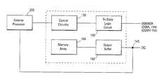
- one embodiment of the present inventionincludes control circuitry 138 , a tri-state logic circuit 190 and an output buffer 192 .
- the tri-state logic circuit 190is used to tri-state the output buffer 192 upon direction of the control circuitry 138 . Tri-stating the output buffer 192 floats the DQ lines 143 . Thus, if the output buffer 192 is tri-stated, data in the DQ lines 143 is not output in response to commands.
- the control circuitry 138signals the tri-state logic circuit 190 to tri-state the output buffer 192 during initialization.
- the tri-state conditionis momentarily overridden during initialization to provide a response to the status command request. That is, once a status command request has been received from the external processor 200 , the tri-state logic circuit stops tri-stating the output buffer 192 until a signal is send through the DQ lines 143 to the external processor 200 indicating that the memory 104 is conducting an initialization operation. Once the signal has been sent, the tri-state logic circuit 190 once again tri-states the output buffer 192 until another status command request is received or until the memory 104 has completed initialization. Once the external processor 200 receives a signal back from the memory 104 that initialization is complete, the external processor 200 begins accessing the memory.
- control circuitry 148may direct the tri-state logic circuit 190 to tri-state state the output buffer 192 for a specific period of time once initialization has commenced.
- the tri-state logic circuitis also coupled to the DQMASK connections (DQML 154 and DQMH 156 ).
- the DQMASK connections 154 and 156allow the output buffer 192 to be manually tri-stated with external commands. This provides the user with the ability to toggle the output signal.
- the DQMASK connections 154 and 156can be used to mask a portion of data that needs to be blocked from being written.
- a tri-state logic circuitis used to selectively tri-state an output buffer during memory initialization.
- the output bufferis used to output data from a memory array to DQ lines. Tri-stating the output buffer floats the DQ lines. Thus, data in the DQ lines is not output in response to commands.
- Control circuitrysignals the tri-state logic circuit to tri-state the output buffer during initialization.
- an external processorcan be used to provide a read status command to the memory to determine the status of memory initialization. In this embodiment, tri-stating the output buffer during initialization is momentarily overridden to respond to the read status command.
Landscapes
- Read Only Memory (AREA)
- Dram (AREA)
Abstract
Description
- This Application is a Continuation of U.S. application Ser. No. 09/802,269 (allowed) filed Mar. 8, 2001. The present invention relates generally to memory devices and in particular the present invention relates to tri-stating an output buffer during initialization of a synchronous memory.[0001]
- Memory devices are typically provided as internal storage areas in the computer. The term “memory” identifies data storage that comes in the form of integrated circuit chips. There are several different types of memory. One type is RAM (random-access memory). This is typically used as main memory in a computer environment. RAM refers to read and write memory; that is, you can both write data into RAM, and read data from RAM. This is in contrast to ROM, which permits you only to read data. Most RAM is volatile, which means that it requires a steady flow of electricity to maintain its contents. As soon as the power is turned off, whatever data was in RAM is lost.[0002]
- Computers almost always contain a small amount of read-only memory (ROM) that holds instructions for starting up the computer. Unlike RAM, ROM cannot be written to. An EEPROM (electrically erasable programmable read-only memory) is a special type non-volatile ROM that can be erased by exposing it to an electrical charge. Like other types of ROM, EEPROM is traditionally not as fast as RAM. EEPROM comprise a large number of memory cells having electrically isolated gates (floating gates). Data is stored in the memory cells in the form of charge on the floating gates. Charge is transported to or removed from the floating gates by programming and erase operations, respectively. at a time. Many modern PCS have their BIOS stored on a flash memory chip so that it can easily be updated if necessary. Such a BIOS is sometimes called a flash BIOS. Flash memory is also popular in modems because it enables the modem manufacturer to support new protocols as they become standardized.[0003]
- A typical Flash memory comprises a memory array that includes a large number of memory cells arranged in row and column fashion. Each of the memory cells includes a floating gate field-effect transistor capable of holding a charge. The cells are usually grouped into blocks. Each of the cells within a block can be electrically programmed in a random basis by charging the floating gate. The charge can be removed from the floating gate by a block erase operation. The data in a cell is determined by the presence or absence of the charge in the floating gate.[0004]
- A synchronous DRAM (SDRAM) is a type of DRAM that can run at much higher clock speeds than conventional DRAM memory. SDRAM synchronizes itself with a CPU's bus and is capable of running at 100 MHZ, about three times faster than conventional FPM (Fast Page Mode) RAM, and about twice as fast EDO (Extended Data Output) DRAM and BEDO (Burst Extended Data Output) DRAM. SDRAM's can be accessed quickly, but are volatile. Many computer systems are designed to operate using SDRAM, but would benefit from non-volatile memory.[0005]
- Generally, all synchronized memory devices require system circuits within the device to be initialized before the memory can be powered up for reliable operation. The initialization process generally includes setting registers for proper operations. It takes a period of time to complete the initialization process. During this time, the memory device can have unknown internal signals and data states. As a result of the unknown states, non-valid data may be sent through output buffers of the memory system causing the system to read faulty data.[0006]
- For the reasons stated above, and for other reasons stated below which will become apparent to those skilled in the art upon reading and understanding the present specification, there is a need in the art for a memory that avoids erroneous output while internal initialization is taking place.[0007]
- The above-mentioned problems with non-valid data being sent during initialization and other problems are addressed by the present invention and will be understood by reading and studying the following specification.[0008]
- In one embodiment, the present invention provides a synchronous memory device that comprises a memory array, an output buffer that outputs data from the memory array, a tri-state logic circuit that selectively tri-states the output buffer and control circuitry to signal the tri-state logic circuit to tri-state the output buffer during memory initialization. The synchronous memory device can also include a pair of DQMASK connections to signal the tri-state logic circuit to tri-state the output buffer manually with external commands.[0009]
- In another embodiment, a synchronous flash memory device comprises, a memory array of non-volatile memory cells, an output buffer to output data from the memory array, a tri-state logic circuit to selectively tri-state the output buffer during initialization and control circuitry to signal the tri-state logic circuit to tri-state the output buffer during memory initialization.[0010]
- In another embodiment, a memory system comprises an external processor and[0011]
- a synchronous memory that is coupled to the external processor. The synchronous memory comprises a memory array, an output buffer to output data from the memory array, a tri-state logic circuit to selectively tri-state the output buffer and control circuitry to signal the tri-state logic circuit to tri-state the output buffer during memory initialization. The memory system can also include the external processor providing a read status command to the memory to determine the status of memory initialization.[0012]
- A method of operating a non-volatile memory that includes tri-stating an output buffer of the memory while the memory is being initialized. One method including starting initialization of the memory, tri-stating an output buffer of the memory, finishing initialization of the memory and returning the output buffer to normal operation after initialization of memory is completed.[0013]
- Another method of operating a memory system includes starting initialization of a memory, tri-stating an output buffer during initialization of the memory, polling the memory to verify the status of initialization, and allowing an external processor to access the memory upon verification of completion of memory initialization. Optionally, the method can include overriding the tri-state condition of the output buffer to signal the external processor that initialization is occurring.[0014]
- FIG. 1 is a block diagram of a synchronous flash memory of the present invention.[0015]
- FIG. 2 is an integrated circuit pin interconnect diagram of one embodiment of the present invention.[0016]
- FIG. 3 is a block diagram of the present invention.[0017]
- In the following detailed description of the preferred embodiments, reference is made to the accompanying drawings that form a part hereof, and in which is shown by way of illustration specific preferred embodiments in which the inventions may be practiced. These embodiments are described in sufficient detail to enable those skilled in the art to practice the invention, and it is to be understood that other embodiments may be utilized and that logical, mechanical and electrical changes may be made without departing from the spirit and scope of the present invention. The following detailed description is, therefore, not to be taken in a limiting sense, and the scope of the present invention is defined only by the claims.[0018]
- Most synchronous memory devices require initialization of the system circuits before the system becomes operational. An example of a recently developed synchronous memory requiring initialization is a synchronous Flash memory. A synchronous Flash memory combines the non-volatile storage capabilities of Flash memory with an[0019]
SDRAM 100 mHz read-compatible interface. - Referring to FIG. 1, a block diagram of one embodiment of a synchronous Flash memory is described. The[0020]
memory device 100 includes an array of non-volatileflash memory cells 102. The array is arranged in a plurality of addressable banks. In one embodiment, the memory contains fourmemory banks address register 112 via address signal connections. The addresses are decoded using rowaddress multiplexer circuitry 114. The addresses are also decoded usingbank control logic 116 and row address latch and decodecircuitry 118. To access an appropriate column of the memory, column address counter andlatch circuitry 120 couples the received addresses tocolumn decode circuitry 122.Circuit 124 provides input/output gating, read data latch circuitry and write driver circuitry. Data is input through data input registers126 and output throughcircuit 128 via data connections.Circuit 128 includes data output registers, an output driver and anoutput buffer 192. Command execution logic130 is provided to control the basic operations of the memory device. Astate machine 132 is also provided to control specific operations performed on the memory array and cells. A status register134 and an identification register136 can also be provided to output data. The command circuit130 and/orstate machine 132 can be generally referred to ascontrol circuitry 138 to control read, write, erase and other memory operations. The data connections are typically used for bi-directional data communication. The memory can be coupled to anexternal processor 200 for operation or testing. - FIG. 2 illustrates an interconnect pin assignment of a synchronous Flash memory. The[0021]
memory package 150 has 54 interconnect pins. The pin configuration is substantially similar to available SDRAM packages. Although they may share interconnect labels that appear the same as SDRAM's, the function of the signals provided on the interconnects are described herein and should not be equated to SDRAM's unless set forth herein. - Prior to describing the operational features of the memory device, a more detailed description of the interconnect pins and their respective signals is provided. The input clock connection is used to provide a clock signal (CLK). A system clock can drive the clock signal, and all synchronous flash memory input signals are sampled on the positive edge of CLK. CLK also increments an internal burst counter and controls the output registers.[0022]
- The input/output mask (DQMASK) connections are used to provide input mask signals for write accesses and an output enable signal for read accesses. Input data is masked when DQMASK is sampled HIGH during a WRITE cycle. The output buffers are placed in a high impedance (High-Z) state (after a two-clock latency) when DQMASK is sampled HIGH during a READ cycle.[0023]
DQML 154 corresponds to lower address data connections DQO-DQ7 andDQMH 156 corresponds to upper address data connections DQ8-DQ15.DQML 154 andDQMH 156 are considered to be the same state when referenced as DQM. - A reset input (RP#)[0024]
connection 140 is used for reset and power-down operations. The RP# signal clears the status register, sets the internal state machine (ISM)132 to an array read mode, and places the device in a deep power-down mode when LOW. During power down, all input connections, including CS#142, are “Don't Care” and all outputs are placed in a High-Z state. When the RP# signal is equal to a VHH voltage (5V), all protection modes are ignored during WRITE and ERASE. The RP# signal also allows a device protect bit to be set to 1 (protected) and allows block protect bits of a 16 bit register, atlocations 0 and15 to be set to 0 (unprotected) when brought to VHH. The protect bits are described in more detail below. RP# is held HIGH during all other modes of operation. - Bank address input connections, BAO and BA[0025]1 define which bank an ACTIVE, READ, WRITE, or BLOCK PROTECT command is being applied. The DQ0-
DQ15 connections 143 are data bus connections used for bi-directional data communication. A VCCQ connection is used to provide isolated power to the DQ connections to improved noise immunity. In one embodiment, VCCQ=Vcc or 1.8V ±0.15V. The VSSQ connection is used to isolated ground to DQs for improved noise immunity. The VCC connection provides a power supply, such as 3V. A ground connection is provided through the Vss connection. Another optional voltage is provided on the VCCP connection144. The VCCP connection can be tied externally to VCC, and sources current during device initialization, WRITE and ERASE operations. That is, writing or erasing to the memory device can be performed using a VCCP voltage, while all other operations can be performed with a VCC voltage. The Vccp connection is coupled to a high voltage switch/pump circuit 145. - Synchronous flash memory has numerous non-volatile storage registers (fuse elements) that contain data used during operation, such as adjusting the internal settings of the device. Some of this information is required before any operation can be performed. Such information could include the location of memory rows or columns in the array that have been replaced with redundant elements. As such, this information must be read at power up. In allowing the information to be read, the information is transferred from the non-volatile storage registers to the volatile storage registers during memory initialization.[0026]
- The synchronous flash memory of FIG. 1 is powered up and initialized in a predefined manner. After power is applied to VCC, VCCQ and VCCP (simultaneously), and the clock signal is stable,[0027]
RP# 140 is brought from a LOW state to a HIGH state. A delay is needed after RP# transitions HIGH in order to complete internal device initialization. Once internal device initialization has been completed, the memory is placed in an array read mode and is ready for Mode Register programming or an executable command. - Initialization of the[0028]
memory 104 takes a specific period of time. A memory system must have a way to deal with this time requirement. One method is by holding off normal operations of thememory 104 for a specific period of time. For example, in one embodiment, a period of 100 μs is set aside for thememory 104 to initialize upon power up. The 100 μs is the time given by the memory system to ensure proper initialization. It will be appreciated by those skilled in the art that the length of initialization will vary with memory designs and that the present invention is not limited to 100 μs. A downfall to this embodiment is that thememory 104 may take less than 100 μs to actually complete initialization. Therefore the extra time given by the memory system for initialization is wasted. - Another way to deal with the initialization time requirement is by monitoring the[0029]
memory 104 to determine when it completes initialization. By monitoring thememory 104, the overall time a memory system takes before it is ready for normal operations can be shortened. For example, if the memory system is given 100 μs to initialize but it only takes 50 μs, the memory system would be ready fornormal operations 50 μs sooner using the monitoring method. In an embodiment that monitors thememory 104, the period of time for initialization is controlled by a read status command from anexternal processor 200. In this embodiment, theexternal processor 200 polls thememory 104, asking thememory 104 if it has completed initialization. If theexternal processor 200 finds that thememory 104 is busy conducting an initialization operation, theexternal processor 200 continues to poll thememory 104. When theexternal processor 200 polls thememory 104 and finds thememory 104 is not performing an initialization operation, theexternal processor 200 begins accessing the memory. - In another embodiment that is designed to shorten the amount of time required before a memory system is ready for normal operations, the[0030]
memory 104 is designed to notify theexternal processor 200 when initialization has been completed. Thememory 104 in this embodiment provides an output signal on itsDQ lines 143 that indicates the completion of initialization for theexternal processor 200 to read. Thus, theexternal processor 200 is notified once the initialization of thememory 104 has been completed. Theexternal processor 200 can then begin accessing thememory 104. - A problem can occur during the time the[0031]
memory 104 is being initialized, as thememory 104 generally has a lot of unknown states during that period of time. As a result of the unknown states, non-valid data may be sent through theoutput buffer 192. The present invention tri-states anoutput buffer 192 of a memory system during initialization to prevent the memory system from reading faulty data. It will be appreciated by those skilled in the art that noise signals can be present on both control lines and data buses. The present invention helps reduce the noise experienced on the memory data bus. That is, the generation of additional noise on the data bus is avoided during initialization in response to faulty input signals. As such, the present invention prevents the memory from compounding existing data bus noise. - As illustrated in FIG. 3, one embodiment of the present invention includes[0032]
control circuitry 138, atri-state logic circuit 190 and anoutput buffer 192. Thetri-state logic circuit 190 is used to tri-state theoutput buffer 192 upon direction of thecontrol circuitry 138. Tri-stating theoutput buffer 192 floats the DQ lines143. Thus, if theoutput buffer 192 is tri-stated, data in the DQ lines143 is not output in response to commands. Thecontrol circuitry 138 signals thetri-state logic circuit 190 to tri-state theoutput buffer 192 during initialization. - In an embodiment that uses a status command request from an[0033]
external processor 200 to poll thememory 104 once initialization has started, the tri-state condition is momentarily overridden during initialization to provide a response to the status command request. That is, once a status command request has been received from theexternal processor 200, the tri-state logic circuit stops tri-stating theoutput buffer 192 until a signal is send through theDQ lines 143 to theexternal processor 200 indicating that thememory 104 is conducting an initialization operation. Once the signal has been sent, thetri-state logic circuit 190 once again tri-states theoutput buffer 192 until another status command request is received or until thememory 104 has completed initialization. Once theexternal processor 200 receives a signal back from thememory 104 that initialization is complete, theexternal processor 200 begins accessing the memory. - In an alternative embodiment, the control circuitry[0034]148 may direct the
tri-state logic circuit 190 to tri-state state theoutput buffer 192 for a specific period of time once initialization has commenced. By setting a defined time period for initialization of amemory 104, the need to have the memory send a signal upon completion of initialization or the need to monitor thememory 104 for completion of initialization is eliminated. - As illustrated in FIG. 3, the tri-state logic circuit is also coupled to the DQMASK connections ([0035]
DQML 154 and DQMH156). TheDQMASK connections output buffer 192 to be manually tri-stated with external commands. This provides the user with the ability to toggle the output signal. For example, theDQMASK connections - A synchronous memory device that avoids generating erroneous output signals while internal initialization is taking place has been described. In one embodiment, a tri-state logic circuit is used to selectively tri-state an output buffer during memory initialization. The output buffer is used to output data from a memory array to DQ lines. Tri-stating the output buffer floats the DQ lines. Thus, data in the DQ lines is not output in response to commands. Control circuitry signals the tri-state logic circuit to tri-state the output buffer during initialization. In another embodiment, an external processor can be used to provide a read status command to the memory to determine the status of memory initialization. In this embodiment, tri-stating the output buffer during initialization is momentarily overridden to respond to the read status command.[0036]
Claims (15)
Priority Applications (1)
| Application Number | Priority Date | Filing Date | Title |
|---|---|---|---|
| US10/352,397US6938117B2 (en) | 2001-03-08 | 2003-01-28 | Tri-stating output buffer during initialization of synchronous memory |
Applications Claiming Priority (2)
| Application Number | Priority Date | Filing Date | Title |
|---|---|---|---|
| US09/802,269US6549975B2 (en) | 2001-03-08 | 2001-03-08 | Tri-stating output buffer during initialization of synchronous memory |
| US10/352,397US6938117B2 (en) | 2001-03-08 | 2003-01-28 | Tri-stating output buffer during initialization of synchronous memory |
Related Parent Applications (1)
| Application Number | Title | Priority Date | Filing Date |
|---|---|---|---|
| US09/802,269ContinuationUS6549975B2 (en) | 2001-03-08 | 2001-03-08 | Tri-stating output buffer during initialization of synchronous memory |
Publications (2)
| Publication Number | Publication Date |
|---|---|
| US20030115427A1true US20030115427A1 (en) | 2003-06-19 |
| US6938117B2 US6938117B2 (en) | 2005-08-30 |
Family
ID=25183261
Family Applications (2)
| Application Number | Title | Priority Date | Filing Date |
|---|---|---|---|
| US09/802,269Expired - LifetimeUS6549975B2 (en) | 2001-03-08 | 2001-03-08 | Tri-stating output buffer during initialization of synchronous memory |
| US10/352,397Expired - LifetimeUS6938117B2 (en) | 2001-03-08 | 2003-01-28 | Tri-stating output buffer during initialization of synchronous memory |
Family Applications Before (1)
| Application Number | Title | Priority Date | Filing Date |
|---|---|---|---|
| US09/802,269Expired - LifetimeUS6549975B2 (en) | 2001-03-08 | 2001-03-08 | Tri-stating output buffer during initialization of synchronous memory |
Country Status (1)
| Country | Link |
|---|---|
| US (2) | US6549975B2 (en) |
Cited By (4)
| Publication number | Priority date | Publication date | Assignee | Title |
|---|---|---|---|---|
| EP1553500A1 (en)* | 2004-01-07 | 2005-07-13 | Deutsche Thomson-Brandt Gmbh | Method and apparatus for indication of valid data |
| US8489837B1 (en)* | 2009-06-12 | 2013-07-16 | Netlist, Inc. | Systems and methods for handshaking with a memory module |
| US20150067315A1 (en)* | 2013-08-30 | 2015-03-05 | SK Hynix Inc. | Memory apparatus and computer system including the same |
| KR20180014947A (en)* | 2016-08-02 | 2018-02-12 | 에스케이하이닉스 주식회사 | Semiconductor device and semiconductor system |
Families Citing this family (5)
| Publication number | Priority date | Publication date | Assignee | Title |
|---|---|---|---|---|
| US6549975B2 (en)* | 2001-03-08 | 2003-04-15 | Micron Technology, Inc. | Tri-stating output buffer during initialization of synchronous memory |
| DE10139085A1 (en)* | 2001-08-16 | 2003-05-22 | Infineon Technologies Ag | Printed circuit board system, method for operating a printed circuit board system, printed circuit board device and its use, and semiconductor device and its use |
| US6751139B2 (en)* | 2002-05-29 | 2004-06-15 | Micron Technology, Inc. | Integrated circuit reset circuitry |
| TWI279256B (en)* | 2005-12-13 | 2007-04-21 | Ind Tech Res Inst | A compact spray cooling module |
| US20100115181A1 (en)* | 2008-11-04 | 2010-05-06 | Sony Ericsson Mobile Communications Ab | Memory device and method |
Citations (11)
| Publication number | Priority date | Publication date | Assignee | Title |
|---|---|---|---|---|
| US4862350A (en)* | 1984-08-03 | 1989-08-29 | International Business Machines Corp. | Architecture for a distributive microprocessing system |
| US5224124A (en)* | 1983-06-16 | 1993-06-29 | Hitachi, Ltd. | Data transmission system |
| US5615159A (en)* | 1995-11-28 | 1997-03-25 | Micron Quantum Devices, Inc. | Memory system with non-volatile data storage unit and method of initializing same |
| US5736867A (en)* | 1996-06-04 | 1998-04-07 | Cypress Semiconductor Corporation | Method and circuit for reconfiguring a buffer |
| US5751641A (en)* | 1995-12-27 | 1998-05-12 | Sgs-Thomson Microelectronics, Inc. | Microprocessor memory test circuit and method |
| US5760607A (en)* | 1995-07-10 | 1998-06-02 | Xilinx, Inc. | System comprising field programmable gate array and intelligent memory |
| US5875353A (en)* | 1992-06-17 | 1999-02-23 | Texas Instruments Incorporated | Circuit with switch controller that signals switch control input to close switch upon completing request acknowledgment of connection request from data transfer port |
| US5983314A (en)* | 1997-07-22 | 1999-11-09 | Micron Technology, Inc. | Output buffer having inherently precise data masking |
| US6178501B1 (en)* | 1998-04-28 | 2001-01-23 | Micron Technology. Inc. | Method and apparatus for initializing a memory device |
| US6246623B1 (en)* | 1998-04-28 | 2001-06-12 | Micron Technology, Inc. | Method and apparatus for strobing antifuse circuits in a memory device |
| US6246626B1 (en)* | 2000-07-28 | 2001-06-12 | Micron Technology, Inc. | Protection after brown out in a synchronous memory |
Family Cites Families (8)
| Publication number | Priority date | Publication date | Assignee | Title |
|---|---|---|---|---|
| US4627054A (en)* | 1984-08-27 | 1986-12-02 | International Business Machines Corporation | Multiprocessor array error detection and recovery apparatus |
| JP2922370B2 (en)* | 1992-10-13 | 1999-07-19 | シャープ株式会社 | Output circuit |
| US5469376A (en)* | 1993-10-14 | 1995-11-21 | Abdallah; Mohammad A. F. F. | Digital circuit for the evaluation of mathematical expressions |
| US6052321A (en)* | 1997-04-16 | 2000-04-18 | Micron Technology, Inc. | Circuit and method for performing test on memory array cells using external sense amplifier reference current |
| US5661690A (en)* | 1996-02-27 | 1997-08-26 | Micron Quantum Devices, Inc. | Circuit and method for performing tests on memory array cells using external sense amplifier reference current |
| US5729169A (en)* | 1996-07-10 | 1998-03-17 | Micron Quantum Devices, Inc. | Controllable one-shot circuit and method for controlling operation of memory circuit using same |
| US6307790B1 (en)* | 2000-08-30 | 2001-10-23 | Micron Technology, Inc. | Read compression in a memory |
| US6549975B2 (en)* | 2001-03-08 | 2003-04-15 | Micron Technology, Inc. | Tri-stating output buffer during initialization of synchronous memory |
- 2001
- 2001-03-08USUS09/802,269patent/US6549975B2/ennot_activeExpired - Lifetime
- 2003
- 2003-01-28USUS10/352,397patent/US6938117B2/ennot_activeExpired - Lifetime
Patent Citations (12)
| Publication number | Priority date | Publication date | Assignee | Title |
|---|---|---|---|---|
| US5224124A (en)* | 1983-06-16 | 1993-06-29 | Hitachi, Ltd. | Data transmission system |
| US4862350A (en)* | 1984-08-03 | 1989-08-29 | International Business Machines Corp. | Architecture for a distributive microprocessing system |
| US5875353A (en)* | 1992-06-17 | 1999-02-23 | Texas Instruments Incorporated | Circuit with switch controller that signals switch control input to close switch upon completing request acknowledgment of connection request from data transfer port |
| US5760607A (en)* | 1995-07-10 | 1998-06-02 | Xilinx, Inc. | System comprising field programmable gate array and intelligent memory |
| US5615159A (en)* | 1995-11-28 | 1997-03-25 | Micron Quantum Devices, Inc. | Memory system with non-volatile data storage unit and method of initializing same |
| US5677885A (en)* | 1995-11-28 | 1997-10-14 | Micron Quantum Devices, Inc. | Memory system with non-volatile data storage unit and method of initializing same |
| US5751641A (en)* | 1995-12-27 | 1998-05-12 | Sgs-Thomson Microelectronics, Inc. | Microprocessor memory test circuit and method |
| US5736867A (en)* | 1996-06-04 | 1998-04-07 | Cypress Semiconductor Corporation | Method and circuit for reconfiguring a buffer |
| US5983314A (en)* | 1997-07-22 | 1999-11-09 | Micron Technology, Inc. | Output buffer having inherently precise data masking |
| US6178501B1 (en)* | 1998-04-28 | 2001-01-23 | Micron Technology. Inc. | Method and apparatus for initializing a memory device |
| US6246623B1 (en)* | 1998-04-28 | 2001-06-12 | Micron Technology, Inc. | Method and apparatus for strobing antifuse circuits in a memory device |
| US6246626B1 (en)* | 2000-07-28 | 2001-06-12 | Micron Technology, Inc. | Protection after brown out in a synchronous memory |
Cited By (13)
| Publication number | Priority date | Publication date | Assignee | Title |
|---|---|---|---|---|
| EP1553500A1 (en)* | 2004-01-07 | 2005-07-13 | Deutsche Thomson-Brandt Gmbh | Method and apparatus for indication of valid data |
| US10474595B2 (en) | 2009-06-12 | 2019-11-12 | Netlist, Inc. | Memory module having an open-drain output pin for parity error in a first mode and for training sequences in a second mode |
| US9311116B1 (en)* | 2009-06-12 | 2016-04-12 | Netlist, Inc. | Systems and methods for handshaking with a memory module |
| US9535623B1 (en) | 2009-06-12 | 2017-01-03 | Netlist, Inc. | Memory module capable of handshaking with a memory controller of a host system |
| US9858218B1 (en)* | 2009-06-12 | 2018-01-02 | Netlist, Inc. | Memory module and methods for handshaking with a memory controller |
| US8489837B1 (en)* | 2009-06-12 | 2013-07-16 | Netlist, Inc. | Systems and methods for handshaking with a memory module |
| US11386024B2 (en) | 2009-06-12 | 2022-07-12 | Netlist, Inc. | Memory module having an open-drain output for parity error and for training sequences |
| US11880319B2 (en) | 2009-06-12 | 2024-01-23 | Netlist, Inc. | Memory module having open-drain output for error reporting and for initialization |
| US20150067315A1 (en)* | 2013-08-30 | 2015-03-05 | SK Hynix Inc. | Memory apparatus and computer system including the same |
| CN104424138A (en)* | 2013-08-30 | 2015-03-18 | 爱思开海力士有限公司 | Memory apparatus and computer system including the same |
| US9489022B2 (en)* | 2013-08-30 | 2016-11-08 | SK Hynix Inc. | Memory apparatus and computer system including the same |
| KR20180014947A (en)* | 2016-08-02 | 2018-02-12 | 에스케이하이닉스 주식회사 | Semiconductor device and semiconductor system |
| KR102628532B1 (en) | 2016-08-02 | 2024-01-25 | 에스케이하이닉스 주식회사 | Semiconductor device and semiconductor system |
Also Published As
| Publication number | Publication date |
|---|---|
| US6938117B2 (en) | 2005-08-30 |
| US20020129193A1 (en) | 2002-09-12 |
| US6549975B2 (en) | 2003-04-15 |
Similar Documents
| Publication | Publication Date | Title |
|---|---|---|
| US7292480B2 (en) | Memory card having buffer memory for storing testing instruction | |
| US6366521B1 (en) | Protection after brown out in a synchronous memory | |
| US6542427B2 (en) | Power validation for memory devices on power up | |
| US6456542B1 (en) | Synchronous memory status register | |
| US6798710B2 (en) | Synchronous flash memory with virtual segment architecture | |
| US7409493B2 (en) | Top/bottom symmetrical protection scheme for flash | |
| US6711701B1 (en) | Write and erase protection in a synchronous memory | |
| US20060156093A1 (en) | Synchronous memory interface with test code input | |
| US6886071B2 (en) | Status register to improve initialization of a synchronous memory | |
| US20090235012A1 (en) | Using lpddr1 bus as transport layer to communicate to flash | |
| US6938117B2 (en) | Tri-stating output buffer during initialization of synchronous memory | |
| US6697907B1 (en) | Hardware initialization of a synchronous memory | |
| US6675255B1 (en) | Device initialize command for a synchronous memory | |
| KR100438636B1 (en) | Top/bottom symmetrical protection scheme for flash |
Legal Events
| Date | Code | Title | Description |
|---|---|---|---|
| FEPP | Fee payment procedure | Free format text:PAYOR NUMBER ASSIGNED (ORIGINAL EVENT CODE: ASPN); ENTITY STATUS OF PATENT OWNER: LARGE ENTITY | |
| STCF | Information on status: patent grant | Free format text:PATENTED CASE | |
| FPAY | Fee payment | Year of fee payment:4 | |
| FPAY | Fee payment | Year of fee payment:8 | |
| AS | Assignment | Owner name:U.S. BANK NATIONAL ASSOCIATION, AS COLLATERAL AGENT, CALIFORNIA Free format text:SECURITY INTEREST;ASSIGNOR:MICRON TECHNOLOGY, INC.;REEL/FRAME:038669/0001 Effective date:20160426 Owner name:U.S. BANK NATIONAL ASSOCIATION, AS COLLATERAL AGEN Free format text:SECURITY INTEREST;ASSIGNOR:MICRON TECHNOLOGY, INC.;REEL/FRAME:038669/0001 Effective date:20160426 | |
| AS | Assignment | Owner name:MORGAN STANLEY SENIOR FUNDING, INC., AS COLLATERAL AGENT, MARYLAND Free format text:PATENT SECURITY AGREEMENT;ASSIGNOR:MICRON TECHNOLOGY, INC.;REEL/FRAME:038954/0001 Effective date:20160426 Owner name:MORGAN STANLEY SENIOR FUNDING, INC., AS COLLATERAL Free format text:PATENT SECURITY AGREEMENT;ASSIGNOR:MICRON TECHNOLOGY, INC.;REEL/FRAME:038954/0001 Effective date:20160426 | |
| FPAY | Fee payment | Year of fee payment:12 | |
| AS | Assignment | Owner name:U.S. BANK NATIONAL ASSOCIATION, AS COLLATERAL AGENT, CALIFORNIA Free format text:CORRECTIVE ASSIGNMENT TO CORRECT THE REPLACE ERRONEOUSLY FILED PATENT #7358718 WITH THE CORRECT PATENT #7358178 PREVIOUSLY RECORDED ON REEL 038669 FRAME 0001. ASSIGNOR(S) HEREBY CONFIRMS THE SECURITY INTEREST;ASSIGNOR:MICRON TECHNOLOGY, INC.;REEL/FRAME:043079/0001 Effective date:20160426 Owner name:U.S. BANK NATIONAL ASSOCIATION, AS COLLATERAL AGEN Free format text:CORRECTIVE ASSIGNMENT TO CORRECT THE REPLACE ERRONEOUSLY FILED PATENT #7358718 WITH THE CORRECT PATENT #7358178 PREVIOUSLY RECORDED ON REEL 038669 FRAME 0001. ASSIGNOR(S) HEREBY CONFIRMS THE SECURITY INTEREST;ASSIGNOR:MICRON TECHNOLOGY, INC.;REEL/FRAME:043079/0001 Effective date:20160426 | |
| AS | Assignment | Owner name:SENTIENT SENSORS LLC, NEW MEXICO Free format text:ASSIGNMENT OF ASSIGNORS INTEREST;ASSIGNOR:BLEMEL TECHNOLOGIES LLC;REEL/FRAME:045382/0714 Effective date:20180125 | |
| AS | Assignment | Owner name:JPMORGAN CHASE BANK, N.A., AS COLLATERAL AGENT, ILLINOIS Free format text:SECURITY INTEREST;ASSIGNORS:MICRON TECHNOLOGY, INC.;MICRON SEMICONDUCTOR PRODUCTS, INC.;REEL/FRAME:047540/0001 Effective date:20180703 Owner name:JPMORGAN CHASE BANK, N.A., AS COLLATERAL AGENT, IL Free format text:SECURITY INTEREST;ASSIGNORS:MICRON TECHNOLOGY, INC.;MICRON SEMICONDUCTOR PRODUCTS, INC.;REEL/FRAME:047540/0001 Effective date:20180703 | |
| AS | Assignment | Owner name:MICRON TECHNOLOGY, INC., IDAHO Free format text:RELEASE BY SECURED PARTY;ASSIGNOR:U.S. BANK NATIONAL ASSOCIATION, AS COLLATERAL AGENT;REEL/FRAME:047243/0001 Effective date:20180629 | |
| AS | Assignment | Owner name:MICRON TECHNOLOGY, INC., IDAHO Free format text:RELEASE BY SECURED PARTY;ASSIGNOR:MORGAN STANLEY SENIOR FUNDING, INC., AS COLLATERAL AGENT;REEL/FRAME:050937/0001 Effective date:20190731 | |
| AS | Assignment | Owner name:MICRON SEMICONDUCTOR PRODUCTS, INC., IDAHO Free format text:RELEASE BY SECURED PARTY;ASSIGNOR:JPMORGAN CHASE BANK, N.A., AS COLLATERAL AGENT;REEL/FRAME:051028/0001 Effective date:20190731 Owner name:MICRON TECHNOLOGY, INC., IDAHO Free format text:RELEASE BY SECURED PARTY;ASSIGNOR:JPMORGAN CHASE BANK, N.A., AS COLLATERAL AGENT;REEL/FRAME:051028/0001 Effective date:20190731 |