US20030113988A1 - Method for manufacturing semiconductor device - Google Patents
Method for manufacturing semiconductor deviceDownload PDFInfo
- Publication number
- US20030113988A1 US20030113988A1US10/289,354US28935402AUS2003113988A1US 20030113988 A1US20030113988 A1US 20030113988A1US 28935402 AUS28935402 AUS 28935402AUS 2003113988 A1US2003113988 A1US 2003113988A1
- Authority
- US
- United States
- Prior art keywords
- semiconductor substrate
- gate electrode
- forming
- layer
- heat treatment
- Prior art date
- Legal status (The legal status is an assumption and is not a legal conclusion. Google has not performed a legal analysis and makes no representation as to the accuracy of the status listed.)
- Granted
Links
Images


Classifications
- H—ELECTRICITY
- H01—ELECTRIC ELEMENTS
- H01L—SEMICONDUCTOR DEVICES NOT COVERED BY CLASS H10
- H01L21/00—Processes or apparatus adapted for the manufacture or treatment of semiconductor or solid state devices or of parts thereof
- H01L21/02—Manufacture or treatment of semiconductor devices or of parts thereof
- H01L21/04—Manufacture or treatment of semiconductor devices or of parts thereof the devices having potential barriers, e.g. a PN junction, depletion layer or carrier concentration layer
- H01L21/18—Manufacture or treatment of semiconductor devices or of parts thereof the devices having potential barriers, e.g. a PN junction, depletion layer or carrier concentration layer the devices having semiconductor bodies comprising elements of Group IV of the Periodic Table or AIIIBV compounds with or without impurities, e.g. doping materials
- H—ELECTRICITY
- H10—SEMICONDUCTOR DEVICES; ELECTRIC SOLID-STATE DEVICES NOT OTHERWISE PROVIDED FOR
- H10D—INORGANIC ELECTRIC SEMICONDUCTOR DEVICES
- H10D62/00—Semiconductor bodies, or regions thereof, of devices having potential barriers
- H10D62/01—Manufacture or treatment
- H10D62/021—Forming source or drain recesses by etching e.g. recessing by etching and then refilling
- H—ELECTRICITY
- H01—ELECTRIC ELEMENTS
- H01L—SEMICONDUCTOR DEVICES NOT COVERED BY CLASS H10
- H01L21/00—Processes or apparatus adapted for the manufacture or treatment of semiconductor or solid state devices or of parts thereof
- H01L21/02—Manufacture or treatment of semiconductor devices or of parts thereof
- H01L21/04—Manufacture or treatment of semiconductor devices or of parts thereof the devices having potential barriers, e.g. a PN junction, depletion layer or carrier concentration layer
- H01L21/18—Manufacture or treatment of semiconductor devices or of parts thereof the devices having potential barriers, e.g. a PN junction, depletion layer or carrier concentration layer the devices having semiconductor bodies comprising elements of Group IV of the Periodic Table or AIIIBV compounds with or without impurities, e.g. doping materials
- H01L21/28—Manufacture of electrodes on semiconductor bodies using processes or apparatus not provided for in groups H01L21/20 - H01L21/268
- H01L21/283—Deposition of conductive or insulating materials for electrodes conducting electric current
- H01L21/285—Deposition of conductive or insulating materials for electrodes conducting electric current from a gas or vapour, e.g. condensation
- H01L21/28506—Deposition of conductive or insulating materials for electrodes conducting electric current from a gas or vapour, e.g. condensation of conductive layers
- H01L21/28512—Deposition of conductive or insulating materials for electrodes conducting electric current from a gas or vapour, e.g. condensation of conductive layers on semiconductor bodies comprising elements of Group IV of the Periodic Table
- H01L21/28518—Deposition of conductive or insulating materials for electrodes conducting electric current from a gas or vapour, e.g. condensation of conductive layers on semiconductor bodies comprising elements of Group IV of the Periodic Table the conductive layers comprising silicides
- H—ELECTRICITY
- H10—SEMICONDUCTOR DEVICES; ELECTRIC SOLID-STATE DEVICES NOT OTHERWISE PROVIDED FOR
- H10D—INORGANIC ELECTRIC SEMICONDUCTOR DEVICES
- H10D30/00—Field-effect transistors [FET]
- H10D30/01—Manufacture or treatment
- H10D30/021—Manufacture or treatment of FETs having insulated gates [IGFET]
- H10D30/0212—Manufacture or treatment of FETs having insulated gates [IGFET] using self-aligned silicidation
- H—ELECTRICITY
- H01—ELECTRIC ELEMENTS
- H01L—SEMICONDUCTOR DEVICES NOT COVERED BY CLASS H10
- H01L21/00—Processes or apparatus adapted for the manufacture or treatment of semiconductor or solid state devices or of parts thereof
- H01L21/02—Manufacture or treatment of semiconductor devices or of parts thereof
- H01L21/02041—Cleaning
- H01L21/02043—Cleaning before device manufacture, i.e. Begin-Of-Line process
- H01L21/02052—Wet cleaning only
- H—ELECTRICITY
- H01—ELECTRIC ELEMENTS
- H01L—SEMICONDUCTOR DEVICES NOT COVERED BY CLASS H10
- H01L21/00—Processes or apparatus adapted for the manufacture or treatment of semiconductor or solid state devices or of parts thereof
- H01L21/02—Manufacture or treatment of semiconductor devices or of parts thereof
- H01L21/04—Manufacture or treatment of semiconductor devices or of parts thereof the devices having potential barriers, e.g. a PN junction, depletion layer or carrier concentration layer
- H01L21/18—Manufacture or treatment of semiconductor devices or of parts thereof the devices having potential barriers, e.g. a PN junction, depletion layer or carrier concentration layer the devices having semiconductor bodies comprising elements of Group IV of the Periodic Table or AIIIBV compounds with or without impurities, e.g. doping materials
- H01L21/30—Treatment of semiconductor bodies using processes or apparatus not provided for in groups H01L21/20 - H01L21/26
- H01L21/31—Treatment of semiconductor bodies using processes or apparatus not provided for in groups H01L21/20 - H01L21/26 to form insulating layers thereon, e.g. for masking or by using photolithographic techniques; After treatment of these layers; Selection of materials for these layers
- H01L21/3105—After-treatment
- H01L21/311—Etching the insulating layers by chemical or physical means
- H01L21/31105—Etching inorganic layers
- H01L21/31111—Etching inorganic layers by chemical means
- H01L21/31116—Etching inorganic layers by chemical means by dry-etching
Definitions
- the present inventionrelates to a method for manufacturing a semiconductor device, and more particularly, to a method for manufacturing a semiconductor device to improve efficiency and operation speed.
- a region contacted to a transistor driving circuitis made of titanium silicide or cobalt silicide so as to decrease a contact resistance between the transistor and the transistor driving circuit. That is, the cobalt silicide (CoSi 3 ) is formed on a transistor having a gate length of 0.18 ⁇ m or less, which substitutes for tungsten silicide (WSi 2 ) and titanium silicide (TiSi 2 ) that have been used for a prior art transistor.
- the cobalt silicide (CoSi 2 )is formed in the following process steps.
- a silicon substrateis prepared, and impurity ions are injected into the silicon substrate to form source/drain regions.
- a rapid thermal processing (RTP) processis performed on the silicon substrate so as to activate the impurity ions, and a double layer of cobalt (Co) and titanium (Ti) is deposited on the silicon substrate.
- a rapid heat treatment processis performed on the silicon substrate in an atmosphere of N 2 .
- the aforementioned cobalt silicideincreases a saturation current value, so that device turning on/off characteristic is improved, thereby easily driving the device at a low voltage. Also, the contact resistance decreases between a line and the transistor, thereby improving an operation speed of the device. Accordingly, the silicide process is necessary to form a logic device.
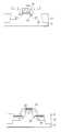
- FIG. 1A to FIG. 1Eare sectional views illustrating the prior art method for manufacturing the semiconductor device.
- an active region and a field regionare defined on a semiconductor substrate 11 .
- the field region of the semiconductor substrate 11is etched at a predetermined depth through photolithography and etching processes, thereby forming a trench.
- the trenchis filled with an insulating material, so that a barrier 12 is formed on the field region of the semiconductor substrate 11 .
- a gate insulating layer 13is formed on an entire surface of the semiconductor substrate 11 including the barrier 12 , and a poly silicon layer 14 as a gate electrode is formed on the gate insulating layer 13 .
- n-type or p-type impurity ionsare selectively injected to the poly silicon layer 14 , and a predopping anneal process is performed thereon.
- the poly silicon layer 14 and the gate insulating layer 13are selectively removed through photolithography and etching processes, thereby forming the gate electrode 14 a .
- lightly doped drain (LDD) ionsare injected to the entire surface of the semiconductor substrate 11 by using the gate electrode 14 a as a mask, thereby forming an LDD region 15 at both sides of the gate electrode 14 a on the surface of the semiconductor substrate 11 . If the semiconductor substrate 11 is in a state of p-type, n-type impurity ions are injected to the semiconductor substrate 11 . Meanwhile, if the semiconductor substrate 11 is in a state of n-type, p-type impurity ions are injected to the semiconductor substrate 11 .
- a cobalt layer 18 and a titanium layer 19are sequentially deposited on the entire surface of the semiconductor substrate 11 including the gate electrode 14 a .
- the heat treatmentis performed on the semiconductor substrate 11 , and a cobalt silicide layer 20 is formed on the surface of the semiconductor substrate 11 including the poly silicon layer 14 and source/drain regions 17 .
- the titanium layer 19 and the cobalt layer 18are removed by wet-etching process, which are not reactive on the surfaces of the polysilicon layer 14 and the source/drain regions 17 .
- the silicide layeris distant from a channel region, so that a resistant material increases between the silicide layer and the channel region, thereby deteriorating device quality and operation speed.
- the present inventionis directed to a method for manufacturing a semiconductor device that substantially obviates one or more problems due to limitations and disadvantages of the prior art.
- An object of the present inventionis to provide to a method for manufacturing a semiconductor device, in which a distance is decreased between a silicide layer and a channel region, so that decreasing a resistance material between the silicide layer and the channel region, thereby improving operation speed and device quality.
- a method for manufacturing a semiconductor deviceincludes forming a barrier for isolating devices from one another on a semiconductor substrate; forming a gate electrode by selectively removing a gate insulating layer on the semiconductor substrate; forming LDD regions at both sides of the gate electrode on the semiconductor substrate; forming an insulating layer on an entire surface of the semiconductor substrate including the gate electrode; forming sidewall spacer at both sides of the gate electrode by selectively removing the insulating layer, simultaneously, etching the semiconductor substrate at a predetermined thickness; performing a cleaning process on the semiconductor substrate; forming source and drain regions at both sides of the gate electrode on the semiconductor substrate; performing PAI process on the entire surface of the semiconductor substrate; and forming a metal silcide layer on surfaces of the gate electrode and the source/drain regions.
- the method according to the present inventionfurther includes depositing an oxide layer on the entire surface of the semiconductor substrate before PAI process, and selectively removing the oxide layer on the semiconductor substrate except for portions of input and output terminals through photolithography and etching processes.
- a gas mixing CHF 3 , CF 4 and Aris used for selectively removing the insulating layer.
- a method for forming the metal silicide layerincludes sequentially depositing first and second metal layers on the entire surface of the semiconductor substrate including the gate electrode, forming the metal silicide layer on the gate electrode and source/drain regions through a first heat treatment on the semiconductor substrate, removing the first and second metal layers that are not reactive on the gate electrode and source/drain regions, and performing a second heat treatment on the semiconductor substrate.
- the first metal layeris made of cobalt
- the second metal layeris made of titanium
- the first heat treatmentis performed at a lower temperature as compared to the second heat treatment.
- a wet etch processis performed with the solution mixing NH 3 OH, H 2 O 2 and H 2 O, and then is performed with a solution mixing HCI, H 2 O 2 and H 2 O.
- FIG. 1A to FIG. 1Eare views illustrating manufacturing process steps of a prior art semiconductor device.
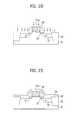
- FIG. 2A to FIG. 2Gare views illustrating manufacturing process steps of a semiconductor device according to the present invention.
- FIG. 2A to FIG. 2Gare views illustrating manufacturing process steps of a semiconductor device according to the present invention.
- an active region and a field regionare defined on a semiconductor substrate 31 , and a barrier 32 is formed on the field region of the semiconductor substrate 31 .
- the field region of the semiconductor substrate 31is etched at a predetermined depth through photolithography and etching processes, thereby forming a trench.
- the trenchis filled with an insulating material, thereby forming the barrier 32 .
- the barrier 32may be formed in a LOCal Oxidation of Silicon (LOCOS) method.
- LOCOSLOCal Oxidation of Silicon
- a gate insulating layer 33is formed on an entire surface of the semiconductor substrate 31 including the barrier 32 , and a poly silicon layer 34 as a gate electrode is formed on the gate insulating layer 33 .
- n-type impurity ions or n-type impurity ionsare selectively injected into the poly silicon layer 34 .
- both NMOS transistor and PMOS transistorare formed on the semiconductor substrate, a mask is formed on a first region of the semiconductor substrate on which the NMOS transistor is formed. Then, n-type impurity ions are injected to a second region of the semiconductor substrate on which the PMOS transistor is formed, and a mask is formed on the second region. After that, p-type impurity ions are injected to the first region of the semiconductor substrate. On the contrary, p-type impurity ions are firstly injected to the first region of the semiconductor substrate, and then n-type impurity ions are injected to the second region of the semiconductor substrate. After injecting the n-type and p-type impurity ions on the semiconductor substrate, an anneal process is performed to activate the n-type and p-type impurity ions.
- the poly silicon layer 34 and the gate insulating layer 33are selectively removed through photolithography and etching processes, thereby forming a gate electrode 34 a .
- lightly doped drain impurity ionsare injected to the entire surface of the semiconductor substrate 31 by using the gate electrode 34 a as the mask, thereby forming an LDD region 35 at both sides of the gate electrode 34 a . If the semiconductor substrate 31 is in a state of P-type, n-type impurity ions are injected to the semiconductor substrate as impurity ions for forming the LDD region.
- the semiconductor substrate 31is in a state of N-type, P-type impurity ions as the LDD impurity ions are injected to the semiconductor substrate. At this time, the LDD impurity ions are injected at an energy of 30 KeV and a dose of 5E15.
- an insulating layer(for example, a nitride layer) is formed on the entire surface of the semiconductor substrate 31 including the gate electrode 34 a , and the etch back process is performed on the entire surface of the semiconductor substrate 31 .
- sidewall spacers 36are formed at both sides of the gate electrode 34 a , and then the semiconductor substrate 31 is removed in both sides of the gate electrode 34 a at a predetermined depth.
- the etch back process for forming the sidewall spacer 36is performed in a dry etch method using CHF 3 , CF 4 or Ar gas.
- CHF 3 or CF 4 gasis used about 300 sccm or less
- Ar gasis used about 2000 sccm or less.
- the etch back processis performed in a vacuum chamber with plasma for 15 seconds.
- a cleaning processis performed on the entire surface of the semiconductor substrate 31 including the sidewall spacer 36 with a solution mixing H 2 O with HF at a ratio of 99 to 1. Also, the cleaning process is performed at a temperature of 25° C.
- n-type impurity ionsfor example, phosphorus P
- a first heat treatmentis performed on the semiconductor substrate to activate the impurity ions injected into the source/drain regions 37 .
- the semiconductor substrateis heated at a temperature between 970° C. and 1040° C. for 10 seconds to 40 seconds in a state of N 2 atmosphere.
- the cleaning processis performed on the entire surface of the semiconductor substrate 31 , thereby removing an oxide layer (not shown) generated during the first heat treatment.
- pre-amorphization Implant (PAI) processis performed so as to decrease poly silicon grain size of the gate electrode 34 a and the semiconductor substrate 31 .
- Ar gasis injected into the semiconductor substrate at energy of 10 KeV to 20 KeV, and a dose of 2E13
- the oxide layerfunctions as a diffusion barrier during a heat treatment process, thereby preventing the silicide layer from being formed.
- the oxide layergenerates serious problems in forming a cobalt silicide layer.
- PAI processis performed to decrease the poly silicon grain size by injecting ions of a heavy element such as Me, As or Ar to the poly silicon before depositing the cobalt layer.
- the cobalt layer 38 and the titanium layer 39are deposited on the entire surface of the semiconductor substrate 31 including the gate electrode 34 a at a thickness of 120 ⁇ to 270 ⁇ in a vacuum state by a physical deposition method.
- a second heat treatmentis performed on the semiconductor substrate 31 , thereby forming a cobalt silicide layer 40 on the surface of the semiconductor substrate 31 including the gate electrode 34 a and source/drain region 37 .
- the semiconductor substrateis heated in a state of NH 3 , N 2 or Ar atmosphere at a temperature of 500° C. to 630° C. for several seconds by a rapid heat treatment device.
- the titanium layer 39 and cobalt layer 38are not reactive on the poly silicon layer 34 and the source/drain region 37 , so that the titanium layer 39 and cobalt layer 38 are removed in a wet etch process.
- the wet etch processis performed with a solution mixing NH 4 OH, H 2 O 2 and H 2 O at a ratio of 1:5:50 for 14 minutes or more, and then is performed with a solution mixing HCI, H 2 O 2 and H 2 O at a ratio of 1:1:5.
- the wet etch processis performed at a temperature of 50° C.
- the cobalt silicide layer 40may be formed on the rest of the semiconductor substrate except for portions of input and output terminals. In this method, following process steps may be additionally required, depositing an HLD oxide layer on the semiconductor substrate at a thickness of 500 ⁇ to 1000 ⁇ between PAI cleaning process and the cleaning process, performing photolithography and dry etch processes on the semiconductor substrate to remove the HLD oxide layer on the surface of the semiconductor substrate except for the portion of the input and output terminals, and cleaning the semiconductor substrate for removing foreign matters.
- a third heat treatmentis performed on the entire surface of the semiconductor substrate 31 including the cobalt silcide layer 40 by a rapid heat treatment device.
- the semiconductor substrate 31is heated at a temperature of 740° C. to 780° C. for several seconds.
- the semiconductor substrateis heated twice. If the semiconductor substrate is heated at a high temperature once, the cobalt silicide layer may be formed on undesired portions, the sidewall spacer 36 . Accordingly, the semiconductor substrate is heated at a low temperature between 500° C. and 630° C. in the second heat treatment process, and then is heated at a high temperature between 740° C. and 780° C., thereby forming the cobalt silicide layer 40 having a low resistance value.
- a nitride layer 41is deposited on the entire surface of the semiconductor substrate 31 including the cobalt silicide layer 40 by injecting TEOS gas or ammonia gas into a vacuum chamber in which the semiconductor substrate 31 is provided.
- the method for manufacturing the semiconductor device according to the present inventionhas the following advantages.
- the silicide layeris formed under the sidewall spacer in the source/drain regions, so that the distance between the silicide layer and the channel becomes short, thereby improving electrical characteristic of the device.
- a saturation current of the transistorincreases, so that it is possible to drive the transistor at a low voltage.
- a rapid heat treatmentmay be performed at a lower temperature than the prior art, thereby increasing a process margin.
- boron B doped on the source/drain regions of the PMOSspreads to the gate insulating layer, so that it may generate problems in processing steps, or it may decrease the process margin.
- the rapid heat treatmentis performed at a low temperature, the process margin increases, thereby improving a yield in mass production of the device.
Landscapes
- Engineering & Computer Science (AREA)
- Physics & Mathematics (AREA)
- Condensed Matter Physics & Semiconductors (AREA)
- General Physics & Mathematics (AREA)
- Manufacturing & Machinery (AREA)
- Computer Hardware Design (AREA)
- Microelectronics & Electronic Packaging (AREA)
- Power Engineering (AREA)
- Electrodes Of Semiconductors (AREA)
- Insulated Gate Type Field-Effect Transistor (AREA)
Abstract
Description
- This application claims the benefit of the Korean Application No.2001-79644 filed on Dec. 15, 2001, which is hereby incorporated by reference.[0001]
- 1. Field of the Invention[0002]
- The present invention relates to a method for manufacturing a semiconductor device, and more particularly, to a method for manufacturing a semiconductor device to improve efficiency and operation speed.[0003]
- 2. Discussion of the Related Art[0004]
- Generally, in a field-effect transistor (FET) of an existing metal oxide semiconductor (MOS) structure, a region contacted to a transistor driving circuit is made of titanium silicide or cobalt silicide so as to decrease a contact resistance between the transistor and the transistor driving circuit. That is, the cobalt silicide (CoSi[0005]3) is formed on a transistor having a gate length of 0.18 μm or less, which substitutes for tungsten silicide (WSi2) and titanium silicide (TiSi2) that have been used for a prior art transistor.
- The cobalt silicide (CoSi[0006]2) is formed in the following process steps. A silicon substrate is prepared, and impurity ions are injected into the silicon substrate to form source/drain regions. Subsequently, a rapid thermal processing (RTP) process is performed on the silicon substrate so as to activate the impurity ions, and a double layer of cobalt (Co) and titanium (Ti) is deposited on the silicon substrate. A rapid heat treatment process is performed on the silicon substrate in an atmosphere of N2.
- The aforementioned cobalt silicide increases a saturation current value, so that device turning on/off characteristic is improved, thereby easily driving the device at a low voltage. Also, the contact resistance decreases between a line and the transistor, thereby improving an operation speed of the device. Accordingly, the silicide process is necessary to form a logic device.[0007]
- A prior art method for manufacturing a semiconductor device will be explained with reference to the accompanying drawings.[0008]
- FIG. 1A to FIG. 1E are sectional views illustrating the prior art method for manufacturing the semiconductor device.[0009]
- As shown in FIG. 1A, an active region and a field region are defined on a[0010]
semiconductor substrate 11. The field region of thesemiconductor substrate 11 is etched at a predetermined depth through photolithography and etching processes, thereby forming a trench. Then, the trench is filled with an insulating material, so that abarrier 12 is formed on the field region of thesemiconductor substrate 11. A gate insulating layer13 is formed on an entire surface of thesemiconductor substrate 11 including thebarrier 12, and apoly silicon layer 14 as a gate electrode is formed on the gate insulating layer13. After that, n-type or p-type impurity ions are selectively injected to thepoly silicon layer 14, and a predopping anneal process is performed thereon. - Referring to FIG. 1R, the[0011]
poly silicon layer 14 and the gate insulating layer13 are selectively removed through photolithography and etching processes, thereby forming thegate electrode 14a. Then, lightly doped drain (LDD) ions are injected to the entire surface of thesemiconductor substrate 11 by using thegate electrode 14aas a mask, thereby forming anLDD region 15 at both sides of thegate electrode 14aon the surface of thesemiconductor substrate 11. If thesemiconductor substrate 11 is in a state of p-type, n-type impurity ions are injected to thesemiconductor substrate 11. Meanwhile, if thesemiconductor substrate 11 is in a state of n-type, p-type impurity ions are injected to thesemiconductor substrate 11. - After forming the insulating layer on the entire surface of the[0012]
semiconductor substrate 11 including thegate electrode 14ashown in FIG. 1C, an etching back process is performed on the entire surface of the semiconductor substrate, thereby formingsidewall spacers 16 at both sides of thegate electrode 14a. Subsequently, heavily doped n-type impurity ions are injected into the entire surface of thesemiconductor substrate 11 by using thegate electrode 14aand thesidewall spacer 15 as the mask, so that source/drain regions 17 are formed on the surface of thesemiconductor substrate 11. - As shown in FIG. 1D, a[0013]
cobalt layer 18 and atitanium layer 19 are sequentially deposited on the entire surface of thesemiconductor substrate 11 including thegate electrode 14a. The heat treatment is performed on thesemiconductor substrate 11, and acobalt silicide layer 20 is formed on the surface of thesemiconductor substrate 11 including thepoly silicon layer 14 and source/drain regions 17. Subsequently, thetitanium layer 19 and thecobalt layer 18 are removed by wet-etching process, which are not reactive on the surfaces of thepolysilicon layer 14 and the source/drain regions 17. - However, the prior art method for manufacturing the semiconductor device has the following problems.[0014]
- In the prior art method for manufacturing the semiconductor device, the silicide layer is distant from a channel region, so that a resistant material increases between the silicide layer and the channel region, thereby deteriorating device quality and operation speed.[0015]
- Accordingly, the present invention is directed to a method for manufacturing a semiconductor device that substantially obviates one or more problems due to limitations and disadvantages of the prior art.[0016]
- An object of the present invention is to provide to a method for manufacturing a semiconductor device, in which a distance is decreased between a silicide layer and a channel region, so that decreasing a resistance material between the silicide layer and the channel region, thereby improving operation speed and device quality.[0017]
- Additional advantages, objects, and features of the invention will be set forth in part in the description which follows and in part will become apparent to those having ordinary skill in the art upon examination of the following or may be learned from practice of the invention. The objectives and other advantages of the invention may be realized and attained by the structure particularly pointed out in the written description and claims hereof as well as the appended drawings.[0018]
- To achieve these objects and other advantages and in accordance with the purpose of the invention, as embodied and broadly described herein, a method for manufacturing a semiconductor device according to the present invention includes forming a barrier for isolating devices from one another on a semiconductor substrate; forming a gate electrode by selectively removing a gate insulating layer on the semiconductor substrate; forming LDD regions at both sides of the gate electrode on the semiconductor substrate; forming an insulating layer on an entire surface of the semiconductor substrate including the gate electrode; forming sidewall spacer at both sides of the gate electrode by selectively removing the insulating layer, simultaneously, etching the semiconductor substrate at a predetermined thickness; performing a cleaning process on the semiconductor substrate; forming source and drain regions at both sides of the gate electrode on the semiconductor substrate; performing PAI process on the entire surface of the semiconductor substrate; and forming a metal silcide layer on surfaces of the gate electrode and the source/drain regions.[0019]
- The method according to the present invention further includes depositing an oxide layer on the entire surface of the semiconductor substrate before PAI process, and selectively removing the oxide layer on the semiconductor substrate except for portions of input and output terminals through photolithography and etching processes.[0020]
- Preferably, a gas mixing CHF[0021]3, CF4and Ar is used for selectively removing the insulating layer.
- Also, a method for forming the metal silicide layer includes sequentially depositing first and second metal layers on the entire surface of the semiconductor substrate including the gate electrode, forming the metal silicide layer on the gate electrode and source/drain regions through a first heat treatment on the semiconductor substrate, removing the first and second metal layers that are not reactive on the gate electrode and source/drain regions, and performing a second heat treatment on the semiconductor substrate.[0022]
- Preferably, the first metal layer is made of cobalt, and the second metal layer is made of titanium.[0023]
- Preferably, the first heat treatment is performed at a lower temperature as compared to the second heat treatment.[0024]
- Preferably, in order to remove the first and second metal layers that are not reactive on the gate electrode and the source/drain regions, a wet etch process is performed with the solution mixing NH[0025]3OH, H2O2and H2O, and then is performed with a solution mixing HCI, H2O2and H2O.
- It is to be understood that both the foregoing general description and the following detailed description of the present invention are exemplary and explanatory and are intended to provide further explanation of the invention as claimed.[0026]
- The accompanying drawings, which are included to provide a further understanding of the invention and are incorporated in and constitute a part of this application, illustrate embodiment(s) of the invention and together with the description serve to explain the principle of the invention. In the drawings:[0027]
- FIG. 1A to FIG. 1E are views illustrating manufacturing process steps of a prior art semiconductor device; and[0028]
- FIG. 2A to FIG. 2G are views illustrating manufacturing process steps of a semiconductor device according to the present invention.[0029]
- Reference will now be made in detail to the preferred embodiments of the present invention, examples of which are illustrated in the accompanying drawings. Wherever possible, the same reference numbers will be used throughout the drawings to refer to the same or like parts.[0030]
- FIG. 2A to FIG. 2G are views illustrating manufacturing process steps of a semiconductor device according to the present invention.[0031]
- As shown in FIG. 2A, an active region and a field region are defined on a[0032]
semiconductor substrate 31, and abarrier 32 is formed on the field region of thesemiconductor substrate 31. Then, the field region of thesemiconductor substrate 31 is etched at a predetermined depth through photolithography and etching processes, thereby forming a trench. The trench is filled with an insulating material, thereby forming thebarrier 32. Also, thebarrier 32 may be formed in a LOCal Oxidation of Silicon (LOCOS) method. A gate insulating layer33 is formed on an entire surface of thesemiconductor substrate 31 including thebarrier 32, and apoly silicon layer 34 as a gate electrode is formed on the gate insulating layer33. Then, n-type impurity ions or n-type impurity ions are selectively injected into thepoly silicon layer 34. - If both NMOS transistor and PMOS transistor are formed on the semiconductor substrate, a mask is formed on a first region of the semiconductor substrate on which the NMOS transistor is formed. Then, n-type impurity ions are injected to a second region of the semiconductor substrate on which the PMOS transistor is formed, and a mask is formed on the second region. After that, p-type impurity ions are injected to the first region of the semiconductor substrate. On the contrary, p-type impurity ions are firstly injected to the first region of the semiconductor substrate, and then n-type impurity ions are injected to the second region of the semiconductor substrate. After injecting the n-type and p-type impurity ions on the semiconductor substrate, an anneal process is performed to activate the n-type and p-type impurity ions.[0033]
- As shown in FIG. 2B, the[0034]
poly silicon layer 34 and the gate insulating layer33 are selectively removed through photolithography and etching processes, thereby forming agate electrode 34a. Subsequently, lightly doped drain impurity ions are injected to the entire surface of thesemiconductor substrate 31 by using thegate electrode 34aas the mask, thereby forming anLDD region 35 at both sides of thegate electrode 34a. If thesemiconductor substrate 31 is in a state of P-type, n-type impurity ions are injected to the semiconductor substrate as impurity ions for forming the LDD region. If thesemiconductor substrate 31 is in a state of N-type, P-type impurity ions as the LDD impurity ions are injected to the semiconductor substrate. At this time, the LDD impurity ions are injected at an energy of 30 KeV and a dose of 5E15. - As shown in FIG. 2C, an insulating layer (for example, a nitride layer) is formed on the entire surface of the[0035]
semiconductor substrate 31 including thegate electrode 34a, and the etch back process is performed on the entire surface of thesemiconductor substrate 31. At this time,sidewall spacers 36 are formed at both sides of thegate electrode 34a, and then thesemiconductor substrate 31 is removed in both sides of thegate electrode 34aat a predetermined depth. - The etch back process for forming the[0036]
sidewall spacer 36 is performed in a dry etch method using CHF3, CF4or Ar gas. In this method, CHF3or CF4gas is used about 300 sccm or less, and Ar gas is used about 2000 sccm or less. The etch back process is performed in a vacuum chamber with plasma for 15 seconds. - A cleaning process is performed on the entire surface of the[0037]
semiconductor substrate 31 including thesidewall spacer 36 with a solution mixing H2O with HF at a ratio of 99 to 1. Also, the cleaning process is performed at a temperature of 25° C. - Subsequently, heavily doped impurity ions are injected into the entire surface of the[0038]
semiconductor substrate 31 by using thegate electrode 34aand thesidewall spacer 36 as the mask, thereby forming source/drain regions 37 on the surface of thesemiconductor substrate 31. When the impurity ions are injected to the semiconductor substrate so as to form the source/drain regions 37, p-type impurity ions or n-type impurity ions are selectively injected to thesemiconductor substrate 31 for selectively forming the PMOS transistor or the NMOS transistor. In a case of that PMOS transistor is formed on the semiconductor substrate, p-type impurity ions (for example, boron B) are injected to the semiconductor substrate. In a case of that NMOS transistor is formed on the semiconductor substrate, n-type impurity ions (for example, phosphorus P) are injected on the semiconductor substrate. Subsequently, a first heat treatment is performed on the semiconductor substrate to activate the impurity ions injected into the source/drain regions 37. At this time, the semiconductor substrate is heated at a temperature between 970° C. and 1040° C. for 10 seconds to 40 seconds in a state of N2atmosphere. - As shown in FIG. 2D, the cleaning process is performed on the entire surface of the[0039]
semiconductor substrate 31, thereby removing an oxide layer (not shown) generated during the first heat treatment. Also, pre-amorphization Implant (PAI) process is performed so as to decrease poly silicon grain size of thegate electrode 34aand thesemiconductor substrate 31. At this time, Ar gas is injected into the semiconductor substrate at energy of 10 KeV to 20 KeV, and a dose of 2E13 - If a metal thin film is deposited to form a silcide layer in a state of that the oxide layer is not removed, the oxide layer functions as a diffusion barrier during a heat treatment process, thereby preventing the silicide layer from being formed. The oxide layer generates serious problems in forming a cobalt silicide layer.[0040]
- To solve theses problems, PAI process is performed to decrease the poly silicon grain size by injecting ions of a heavy element such as Me, As or Ar to the poly silicon before depositing the cobalt layer.[0041]
- As shown in FIG. 2E, the[0042]
cobalt layer 38 and thetitanium layer 39 are deposited on the entire surface of thesemiconductor substrate 31 including thegate electrode 34aat a thickness of 120 Å to 270 Å in a vacuum state by a physical deposition method. - Referring to FIG. 2F, a second heat treatment is performed on the[0043]
semiconductor substrate 31, thereby forming acobalt silicide layer 40 on the surface of thesemiconductor substrate 31 including thegate electrode 34aand source/drain region 37. The semiconductor substrate is heated in a state of NH3, N2or Ar atmosphere at a temperature of 500° C. to 630° C. for several seconds by a rapid heat treatment device. - The[0044]
titanium layer 39 andcobalt layer 38 are not reactive on thepoly silicon layer 34 and the source/drain region 37, so that thetitanium layer 39 andcobalt layer 38 are removed in a wet etch process. - At this time, the wet etch process is performed with a solution mixing NH[0045]4OH, H2O2and H2O at a ratio of 1:5:50 for 14 minutes or more, and then is performed with a solution mixing HCI, H2O2and H2O at a ratio of 1:1:5. The wet etch process is performed at a temperature of 50° C.
- During forming the[0046]
cobalt silicide layer 40, thecobalt silicide layer 40 may be formed on the rest of the semiconductor substrate except for portions of input and output terminals. In this method, following process steps may be additionally required, depositing an HLD oxide layer on the semiconductor substrate at a thickness of 500 Å to 1000 Å between PAI cleaning process and the cleaning process, performing photolithography and dry etch processes on the semiconductor substrate to remove the HLD oxide layer on the surface of the semiconductor substrate except for the portion of the input and output terminals, and cleaning the semiconductor substrate for removing foreign matters. - Subsequently, a third heat treatment is performed on the entire surface of the[0047]
semiconductor substrate 31 including thecobalt silcide layer 40 by a rapid heat treatment device. Thesemiconductor substrate 31 is heated at a temperature of 740° C. to 780° C. for several seconds. - In order to form the[0048]
cobalt silicide layer 40 on the semiconductor substrate, the semiconductor substrate is heated twice. If the semiconductor substrate is heated at a high temperature once, the cobalt silicide layer may be formed on undesired portions, thesidewall spacer 36. Accordingly, the semiconductor substrate is heated at a low temperature between 500° C. and 630° C. in the second heat treatment process, and then is heated at a high temperature between 740° C. and 780° C., thereby forming thecobalt silicide layer 40 having a low resistance value. - As shown in FIG. 2G, a[0049]
nitride layer 41 is deposited on the entire surface of thesemiconductor substrate 31 including thecobalt silicide layer 40 by injecting TEOS gas or ammonia gas into a vacuum chamber in which thesemiconductor substrate 31 is provided. - As mentioned above, the method for manufacturing the semiconductor device according to the present invention has the following advantages.[0050]
- First, the silicide layer is formed under the sidewall spacer in the source/drain regions, so that the distance between the silicide layer and the channel becomes short, thereby improving electrical characteristic of the device.[0051]
- Also, a saturation current of the transistor increases, so that it is possible to drive the transistor at a low voltage.[0052]
- In order to obtain the desired saturation current of the transistor, a rapid heat treatment may be performed at a lower temperature than the prior art, thereby increasing a process margin.[0053]
- In fabricating a device having a gate length of 0.18 μm or less, boron B doped on the source/drain regions of the PMOS spreads to the gate insulating layer, so that it may generate problems in processing steps, or it may decrease the process margin. However, if the rapid heat treatment is performed at a low temperature, the process margin increases, thereby improving a yield in mass production of the device.[0054]
- It will be apparent to those skilled in the art that various modifications and variations can be made in the present invention. Thus, it is intended that the present invention covers the modifications and variations of this invention provided they come within the scope of the appended claims and their equivalents.[0055]
Claims (21)
Applications Claiming Priority (2)
| Application Number | Priority Date | Filing Date | Title |
|---|---|---|---|
| KR10-2001-0079644AKR100396709B1 (en) | 2001-12-15 | 2001-12-15 | method for manufacturing of semiconductor device |
| KRP2001-79644 | 2001-12-15 |
Publications (2)
| Publication Number | Publication Date |
|---|---|
| US20030113988A1true US20030113988A1 (en) | 2003-06-19 |
| US6855592B2 US6855592B2 (en) | 2005-02-15 |
Family
ID=19717071
Family Applications (1)
| Application Number | Title | Priority Date | Filing Date |
|---|---|---|---|
| US10/289,354Expired - LifetimeUS6855592B2 (en) | 2001-12-15 | 2002-11-07 | Method for manufacturing semiconductor device |
Country Status (3)
| Country | Link |
|---|---|
| US (1) | US6855592B2 (en) |
| JP (1) | JP2003203927A (en) |
| KR (1) | KR100396709B1 (en) |
Cited By (5)
| Publication number | Priority date | Publication date | Assignee | Title |
|---|---|---|---|---|
| US20050186748A1 (en)* | 2004-01-22 | 2005-08-25 | Kabushiki Kaisha Toshiba | Method of manufacturing semiconductor device |
| US20080206973A1 (en)* | 2007-02-26 | 2008-08-28 | Texas Instrument Inc. | Process method to optimize fully silicided gate (FUSI) thru PAI implant |
| CN102891182A (en)* | 2011-07-22 | 2013-01-23 | 株式会社半导体能源研究所 | Semiconductor device |
| CN115020226A (en)* | 2022-07-19 | 2022-09-06 | 合肥晶合集成电路股份有限公司 | Manufacturing method of semiconductor structure and semiconductor structure |
| US12300729B2 (en)* | 2016-11-29 | 2025-05-13 | Taiwan Semiconductor Manufacturing Company, Ltd. | Low resistant contact method and structure |
Families Citing this family (7)
| Publication number | Priority date | Publication date | Assignee | Title |
|---|---|---|---|---|
| US7361973B2 (en)* | 2004-05-21 | 2008-04-22 | International Business Machines Corporation | Embedded stressed nitride liners for CMOS performance improvement |
| JP4700295B2 (en)* | 2004-06-08 | 2011-06-15 | 富士通セミコンダクター株式会社 | Semiconductor device and manufacturing method thereof |
| JP2007184420A (en)* | 2006-01-06 | 2007-07-19 | Nec Electronics Corp | Manufacturing method of semiconductor device |
| JP4723413B2 (en)* | 2006-04-25 | 2011-07-13 | シャープ株式会社 | Manufacturing method of semiconductor device |
| US7410876B1 (en)* | 2007-04-05 | 2008-08-12 | Freescale Semiconductor, Inc. | Methodology to reduce SOI floating-body effect |
| US7785949B2 (en)* | 2007-06-06 | 2010-08-31 | Taiwan Semiconductor Manufacturing Co., Ltd. | Method for forming semiconductor device using multi-functional sacrificial dielectric layer |
| US20150194311A1 (en)* | 2014-01-08 | 2015-07-09 | Macronix International Co., Ltd. | Method For Manufacturing Semiconductor Device |
Citations (12)
| Publication number | Priority date | Publication date | Assignee | Title |
|---|---|---|---|---|
| US5047367A (en)* | 1990-06-08 | 1991-09-10 | Intel Corporation | Process for formation of a self aligned titanium nitride/cobalt silicide bilayer |
| US5496750A (en)* | 1994-09-19 | 1996-03-05 | Texas Instruments Incorporated | Elevated source/drain junction metal oxide semiconductor field-effect transistor using blanket silicon deposition |
| US5691215A (en)* | 1996-08-26 | 1997-11-25 | Industrial Technology Research Institute | Method for fabricating a sub-half micron MOSFET device with insulator filled shallow trenches planarized via use of negative photoresist and de-focus exposure |
| US5731239A (en)* | 1997-01-22 | 1998-03-24 | Chartered Semiconductor Manufacturing Pte Ltd. | Method of making self-aligned silicide narrow gate electrodes for field effect transistors having low sheet resistance |
| US5763923A (en)* | 1996-08-13 | 1998-06-09 | Micron Technology, Inc. | Compound PVD target material for semiconductor metallization |
| US6051881A (en)* | 1997-12-05 | 2000-04-18 | Advanced Micro Devices | Forming local interconnects in integrated circuits |
| US6194298B1 (en)* | 1999-04-19 | 2001-02-27 | United Semiconductor Corp. | Method of fabricating semiconductor device |
| US6238989B1 (en)* | 2000-03-10 | 2001-05-29 | United Microelectronics Corp. | Process of forming self-aligned silicide on source/drain region |
| US6242333B1 (en)* | 1998-01-06 | 2001-06-05 | Texas Instruments Incorporated | Method to enhance the formation of nucleation sites on silicon structures and an improved silicon structure |
| US6294415B1 (en)* | 2000-04-26 | 2001-09-25 | United Microelectronics Corp. | Method of fabricating a MOS transistor |
| US6326289B1 (en)* | 1998-08-24 | 2001-12-04 | Texas Instruments Incorporated | Method of forming a silicide layer using a pre-amorphization implant which is blocked from source/drain regions by a layer of photoresist |
| US20030003723A1 (en)* | 2001-06-30 | 2003-01-02 | Wan-Gyu Lee | Method for manufacturing semiconductor device |
Family Cites Families (4)
| Publication number | Priority date | Publication date | Assignee | Title |
|---|---|---|---|---|
| JPH09321304A (en)* | 1996-03-22 | 1997-12-12 | Seiko Epson Corp | Semiconductor device including MOS element and manufacturing method thereof |
| JPH10125915A (en)* | 1996-10-24 | 1998-05-15 | Nec Yamagata Ltd | Semiconductor device and its manufacture |
| JP2001036080A (en)* | 1999-07-26 | 2001-02-09 | Mitsubishi Electric Corp | Semiconductor device and manufacturing method thereof |
| JP3515041B2 (en)* | 2000-03-13 | 2004-04-05 | 沖電気工業株式会社 | Method for manufacturing semiconductor device |
- 2001
- 2001-12-15KRKR10-2001-0079644Apatent/KR100396709B1/ennot_activeExpired - Fee Related
- 2002
- 2002-11-07USUS10/289,354patent/US6855592B2/ennot_activeExpired - Lifetime
- 2002-12-06JPJP2002354663Apatent/JP2003203927A/enactivePending
Patent Citations (13)
| Publication number | Priority date | Publication date | Assignee | Title |
|---|---|---|---|---|
| US5047367A (en)* | 1990-06-08 | 1991-09-10 | Intel Corporation | Process for formation of a self aligned titanium nitride/cobalt silicide bilayer |
| US5496750A (en)* | 1994-09-19 | 1996-03-05 | Texas Instruments Incorporated | Elevated source/drain junction metal oxide semiconductor field-effect transistor using blanket silicon deposition |
| US5763923A (en)* | 1996-08-13 | 1998-06-09 | Micron Technology, Inc. | Compound PVD target material for semiconductor metallization |
| US6004879A (en)* | 1996-08-13 | 1999-12-21 | Micron Technology, Inc | Method for fabricating a structure on a cobalt silicide oxide metalization semiconductor substrate |
| US5691215A (en)* | 1996-08-26 | 1997-11-25 | Industrial Technology Research Institute | Method for fabricating a sub-half micron MOSFET device with insulator filled shallow trenches planarized via use of negative photoresist and de-focus exposure |
| US5731239A (en)* | 1997-01-22 | 1998-03-24 | Chartered Semiconductor Manufacturing Pte Ltd. | Method of making self-aligned silicide narrow gate electrodes for field effect transistors having low sheet resistance |
| US6051881A (en)* | 1997-12-05 | 2000-04-18 | Advanced Micro Devices | Forming local interconnects in integrated circuits |
| US6242333B1 (en)* | 1998-01-06 | 2001-06-05 | Texas Instruments Incorporated | Method to enhance the formation of nucleation sites on silicon structures and an improved silicon structure |
| US6326289B1 (en)* | 1998-08-24 | 2001-12-04 | Texas Instruments Incorporated | Method of forming a silicide layer using a pre-amorphization implant which is blocked from source/drain regions by a layer of photoresist |
| US6194298B1 (en)* | 1999-04-19 | 2001-02-27 | United Semiconductor Corp. | Method of fabricating semiconductor device |
| US6238989B1 (en)* | 2000-03-10 | 2001-05-29 | United Microelectronics Corp. | Process of forming self-aligned silicide on source/drain region |
| US6294415B1 (en)* | 2000-04-26 | 2001-09-25 | United Microelectronics Corp. | Method of fabricating a MOS transistor |
| US20030003723A1 (en)* | 2001-06-30 | 2003-01-02 | Wan-Gyu Lee | Method for manufacturing semiconductor device |
Cited By (9)
| Publication number | Priority date | Publication date | Assignee | Title |
|---|---|---|---|---|
| US20050186748A1 (en)* | 2004-01-22 | 2005-08-25 | Kabushiki Kaisha Toshiba | Method of manufacturing semiconductor device |
| US20080206973A1 (en)* | 2007-02-26 | 2008-08-28 | Texas Instrument Inc. | Process method to optimize fully silicided gate (FUSI) thru PAI implant |
| WO2008106397A3 (en)* | 2007-02-26 | 2008-11-27 | Texas Instruments Inc | Process method to optimize fully silicided gate (fusi) thru pai implant |
| CN102891182A (en)* | 2011-07-22 | 2013-01-23 | 株式会社半导体能源研究所 | Semiconductor device |
| US10153378B2 (en) | 2011-07-22 | 2018-12-11 | Semiconductor Energy Laboratory Co., Ltd. | Semiconductor device comprising oxide semiconductor |
| US10991829B2 (en) | 2011-07-22 | 2021-04-27 | Semiconductor Energy Laboratory Co., Ltd. | Semiconductor device comprising oxide semiconductor |
| US12062722B2 (en) | 2011-07-22 | 2024-08-13 | Semiconductor Energy Laboratory Co., Ltd. | Method for fabrication of semiconductor device |
| US12300729B2 (en)* | 2016-11-29 | 2025-05-13 | Taiwan Semiconductor Manufacturing Company, Ltd. | Low resistant contact method and structure |
| CN115020226A (en)* | 2022-07-19 | 2022-09-06 | 合肥晶合集成电路股份有限公司 | Manufacturing method of semiconductor structure and semiconductor structure |
Also Published As
| Publication number | Publication date |
|---|---|
| JP2003203927A (en) | 2003-07-18 |
| KR20030049441A (en) | 2003-06-25 |
| US6855592B2 (en) | 2005-02-15 |
| KR100396709B1 (en) | 2003-09-02 |
Similar Documents
| Publication | Publication Date | Title |
|---|---|---|
| US5956584A (en) | Method of making self-aligned silicide CMOS transistors | |
| JP3238551B2 (en) | Method for manufacturing field effect transistor | |
| US6090653A (en) | Method of manufacturing CMOS transistors | |
| JPH1079506A (en) | Semiconductor device and manufacturing method thereof | |
| US6972222B2 (en) | Temporary self-aligned stop layer is applied on silicon sidewall | |
| US6855592B2 (en) | Method for manufacturing semiconductor device | |
| JP3975297B2 (en) | Method for forming dual gate oxide film and method for manufacturing semiconductor device using the same | |
| US5972761A (en) | Method of making MOS transistors with a gate-side air-gap structure and an extension ultra-shallow S/D junction | |
| JP2008508723A (en) | Manufacturing method of semiconductor device having silicide region | |
| US5747852A (en) | LDD MOS transistor with improved uniformity and controllability of alignment | |
| KR100549006B1 (en) | Manufacturing method of MOS transistor with complete silicide gate | |
| JP2002518827A (en) | Method of manufacturing semiconductor device including MOS transistor | |
| KR100685898B1 (en) | Manufacturing method of semiconductor device | |
| US6674135B1 (en) | Semiconductor structure having elevated salicided source/drain regions and metal gate electrode on nitride/oxide dielectric | |
| KR100690910B1 (en) | Salicide process and method of manufacturing a semiconductor device using the same | |
| KR100192537B1 (en) | Method of manufacturing semiconductor device | |
| JP2968548B2 (en) | Semiconductor device and manufacturing method thereof | |
| JP2004207613A (en) | Semiconductor device and manufacturing method thereof | |
| KR100418571B1 (en) | Method for fabricating MOSFET with lightly doped drain structure | |
| KR100443793B1 (en) | Method of manufacturing a semiconductor device | |
| JP3657532B2 (en) | Manufacturing method of semiconductor device | |
| KR100439191B1 (en) | Method of making salicide contact | |
| KR100565755B1 (en) | Manufacturing method of semiconductor device | |
| KR20020012923A (en) | Method for Forming Self-Aligned Silcide of Semiconductor Device | |
| KR100260360B1 (en) | Method for manufacturing semiconductor device |
Legal Events
| Date | Code | Title | Description |
|---|---|---|---|
| AS | Assignment | Owner name:HYNIX SEMICONDUCTOR INC., KOREA, REPUBLIC OF Free format text:ASSIGNMENT OF ASSIGNORS INTEREST;ASSIGNOR:LEE, WAN GYU;REEL/FRAME:013473/0026 Effective date:20021101 | |
| FEPP | Fee payment procedure | Free format text:PAYOR NUMBER ASSIGNED (ORIGINAL EVENT CODE: ASPN); ENTITY STATUS OF PATENT OWNER: LARGE ENTITY | |
| AS | Assignment | Owner name:MAGNACHIP SEMICONDUCTOR, LTD., KOREA, REPUBLIC OF Free format text:ASSIGNMENT OF ASSIGNORS INTEREST;ASSIGNOR:HYNIX SEMICONDUCTOR, INC.;REEL/FRAME:016216/0649 Effective date:20041004 | |
| STCF | Information on status: patent grant | Free format text:PATENTED CASE | |
| FPAY | Fee payment | Year of fee payment:4 | |
| AS | Assignment | Owner name:U.S. BANK NATIONAL ASSOCIATION, AS COLLATERAL TRUS Free format text:AFTER-ACQUIRED INTELLECTUAL PROPERTY KUN-PLEDGE AGREEMENT;ASSIGNOR:MAGNACHIP SEMICONDUCTOR, LTD.;REEL/FRAME:022277/0133 Effective date:20090217 | |
| FEPP | Fee payment procedure | Free format text:PAYER NUMBER DE-ASSIGNED (ORIGINAL EVENT CODE: RMPN); ENTITY STATUS OF PATENT OWNER: LARGE ENTITY Free format text:PAYOR NUMBER ASSIGNED (ORIGINAL EVENT CODE: ASPN); ENTITY STATUS OF PATENT OWNER: LARGE ENTITY | |
| AS | Assignment | Owner name:MAGNACHIP SEMICONDUCTOR LTD.,KOREA, DEMOCRATIC PEO Free format text:RELEASE BY SECURED PARTY;ASSIGNOR:U.S. BANK NATIONAL ASSOCIATION;REEL/FRAME:024563/0807 Effective date:20100527 | |
| FPAY | Fee payment | Year of fee payment:8 | |
| AS | Assignment | Owner name:MAGNACHIP SEMICONDUCTOR LTD., KOREA, REPUBLIC OF Free format text:CORRECTIVE ASSIGNMENT TO CORRECT THE RECEIVING PARTY ADDRESS PREVIOUSLY RECORDED AT REEL: 024563 FRAME: 0807. ASSIGNOR(S) HEREBY CONFIRMS THE RELEASE BY SECURED PARTY;ASSIGNOR:US BANK NATIONAL ASSOCIATION;REEL/FRAME:034469/0001 Effective date:20100527 | |
| FPAY | Fee payment | Year of fee payment:12 | |
| AS | Assignment | Owner name:KEY FOUNDRY CO., LTD., KOREA, REPUBLIC OF Free format text:ASSIGNMENT OF ASSIGNORS INTEREST;ASSIGNOR:MAGNACHIP SEMICONDUCTOR, LTD.;REEL/FRAME:053703/0227 Effective date:20200828 |