US20030112227A1 - Signal line of touch panel display device and method of forming the same - Google Patents
Signal line of touch panel display device and method of forming the sameDownload PDFInfo
- Publication number
- US20030112227A1 US20030112227A1US10/319,632US31963202AUS2003112227A1US 20030112227 A1US20030112227 A1US 20030112227A1US 31963202 AUS31963202 AUS 31963202AUS 2003112227 A1US2003112227 A1US 2003112227A1
- Authority
- US
- United States
- Prior art keywords
- electrodes
- touch panel
- signal line
- forming
- display device
- Prior art date
- Legal status (The legal status is an assumption and is not a legal conclusion. Google has not performed a legal analysis and makes no representation as to the accuracy of the status listed.)
- Granted
Links
Images


Classifications
- G—PHYSICS
- G06—COMPUTING OR CALCULATING; COUNTING
- G06F—ELECTRIC DIGITAL DATA PROCESSING
- G06F3/00—Input arrangements for transferring data to be processed into a form capable of being handled by the computer; Output arrangements for transferring data from processing unit to output unit, e.g. interface arrangements
- G06F3/01—Input arrangements or combined input and output arrangements for interaction between user and computer
- G06F3/03—Arrangements for converting the position or the displacement of a member into a coded form
- G06F3/041—Digitisers, e.g. for touch screens or touch pads, characterised by the transducing means
- G06F3/045—Digitisers, e.g. for touch screens or touch pads, characterised by the transducing means using resistive elements, e.g. a single continuous surface or two parallel surfaces put in contact
- G—PHYSICS
- G02—OPTICS
- G02F—OPTICAL DEVICES OR ARRANGEMENTS FOR THE CONTROL OF LIGHT BY MODIFICATION OF THE OPTICAL PROPERTIES OF THE MEDIA OF THE ELEMENTS INVOLVED THEREIN; NON-LINEAR OPTICS; FREQUENCY-CHANGING OF LIGHT; OPTICAL LOGIC ELEMENTS; OPTICAL ANALOGUE/DIGITAL CONVERTERS
- G02F1/00—Devices or arrangements for the control of the intensity, colour, phase, polarisation or direction of light arriving from an independent light source, e.g. switching, gating or modulating; Non-linear optics
- G02F1/01—Devices or arrangements for the control of the intensity, colour, phase, polarisation or direction of light arriving from an independent light source, e.g. switching, gating or modulating; Non-linear optics for the control of the intensity, phase, polarisation or colour
- G02F1/13—Devices or arrangements for the control of the intensity, colour, phase, polarisation or direction of light arriving from an independent light source, e.g. switching, gating or modulating; Non-linear optics for the control of the intensity, phase, polarisation or colour based on liquid crystals, e.g. single liquid crystal display cells
- G02F1/133—Constructional arrangements; Operation of liquid crystal cells; Circuit arrangements
- G02F1/1333—Constructional arrangements; Manufacturing methods
- G02F1/1345—Conductors connecting electrodes to cell terminals
- G—PHYSICS
- G06—COMPUTING OR CALCULATING; COUNTING
- G06F—ELECTRIC DIGITAL DATA PROCESSING
- G06F3/00—Input arrangements for transferring data to be processed into a form capable of being handled by the computer; Output arrangements for transferring data from processing unit to output unit, e.g. interface arrangements
- G06F3/01—Input arrangements or combined input and output arrangements for interaction between user and computer
- G06F3/03—Arrangements for converting the position or the displacement of a member into a coded form
- G06F3/041—Digitisers, e.g. for touch screens or touch pads, characterised by the transducing means
- G06F3/047—Digitisers, e.g. for touch screens or touch pads, characterised by the transducing means using sets of wires, e.g. crossed wires
Definitions
- the present inventionrelates to a display device, and more particularly to a signal line of a touch panel display device and method of forming the same.
- a touch panel deviceis a computer peripheral that is commonly installed on a display surface of an image display device such as a cathode ray tube (CRT), a liquid crystal display (LCD), a field emission display (FED), a plasma display panel (PDP), and an electro-luminescence device (ELD) so that while looking at the image display device, a user applies pressure on the touch panel to enter predetermined information into the computer.
- an image display devicesuch as a cathode ray tube (CRT), a liquid crystal display (LCD), a field emission display (FED), a plasma display panel (PDP), and an electro-luminescence device (ELD) so that while looking at the image display device, a user applies pressure on the touch panel to enter predetermined information into the computer.
- CTRcathode ray tube
- LCDliquid crystal display
- FEDfield emission display
- PDPplasma display panel
- ELDelectro-luminescence device
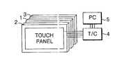
- FIG. 1is a perspective view of a touch panel display device and a liquid crystal display panel according to the related art.
- the touch panel display deviceincludes a touch panel 2 , a liquid crystal panel 1 , and a backlight 3 .
- the touch panel 2is electrically connected to a computer system 5 via a touch controller 4 by signal lines.
- a touch controller 4by signal lines.
- a top of the touch panel 2is contacted with more than a specific pressure
- a voltage value of the contact positionis calculated by the touch controller 4 , thereby calculating coordinates of the contact position.
- FIG. 2is a cross sectional view of the touch panel display device and the liquid crystal display panel of FIG. 1 according to the related art.
- a liquid crystal display panel 1is located between an upper polarized sheet 4 A and a lower polarized sheet 4 B, and the touch panel 2 is placed on the upper polarized sheet 4 A.
- the liquid crystal panel 1includes liquid crystal material 14 and a ball spacer 5 interposed between a lower glass substrate 3 A and an upper glass substrate 3 B.
- a gate line 6 , an insulation film 8 , a pixel electrode 10 A, and a first alignment film 12 Aare sequentially formed on the lower glass substrate 3 A.
- the upper glass substrate 3 Bhas a black matrix 16 , a color filter 18 , a common electrode 17 , and a second alignment film 12 B sequentially formed on a bottom surface thereof.
- the ball spacer 5is sprayed on a first alignment film 12 A before the upper glass substrate 3 B is bonded with the lower glass substrate 3 A.
- the upper glass substrate 3 B and the lower glass substrate 3 Aare separated by the ball spacer 5 to be maintained with a specific gap. That is, the spacer 5 uniformly maintains the gap between the upper glass substrate 3 B and the lower glass substrate 3 A, thereby maintaining a uniform thickness of the liquid crystal material 14 .
- the touch panel 2includes a spacer 28 formed between a lower substrate 20 and an upper substrate 24 .
- a first electrode layer 26is formed on the surface of the lower substrate 20
- a second electrode layer 27is formed on a bottom surface of the upper substrate 24 .
- the second electrode layer 27is electrically shorted with the first electrode layer 26 when the upper substrate 24 is pressed with a stylus pen or a finger, to generate a current or voltage level signal that changes in accordance with the pressed position.
- the first electrode layer 26 and the second electrode layer 27are formed by printing silver Ag on transparent conductive material that has good transmittance, and has a low resistance.
- the first electrode layer 26 and the second electrode layer 27include indium-tin-oxide ITO, indium-zinc-oxide IZO, and indium-tin-zinc-oxide ITZO.
- FIG. 3is a plan view of an electrode and a signal line of the touch panel display device of FIG. 2 according to the related art.
- an upper plate of the touch panel 2includes X-axis electrodes 27 A and 27 B formed along an edge thereof along a vertical direction, and signal lines 28 C and 28 D are derived from a center of the X-axis electrodes 27 A and 27 B for supplying the current or voltage level signal to the touch controller 4 .
- a lower plate of the touch panel 2includes Y-axis electrodes 26 A and 26 B formed along an edge thereof a long a horizontal direction, and signal lines 28 A and 28 B are derived from a center of the Y-axis electrode 26 A and 26 B for supplying the current or voltage level signal to the touch controller 34 .
- FIG. 4is a perspective view of two separate substrates of the touch panel display device of FIG. 3 according to the related art.
- the signal lines 28 A, 28 B, 28 C, and 28 Dinclude a tail part 29 and an electrode extension connected to the electrodes 26 A, 26 B, 27 A, and 27 B. If the two substrates are bonded together as above, then the electrodes 26 A, 26 B, 27 A, and 27 B, and the signal lines 28 A, 28 B, 28 C, and 28 D are arranged together.
- the present inventionis directed to a signal line of a touch panel display device and method of forming the same that substantially obviates one or more of the problems due to limitations and disadvantages of the related art.
- An object of the present inventionis to provide a signal line of a touch panel display device that forms a signal line connected to an electrode of a touch panel using a side portion of the electrode.
- Another object of the present inventionis to provide a method of forming a signal line of a touch panel display device that forms a signal line connected to an electrode of a touch panel using a side portion of the electrode.
- a signal line of a touch panel display deviceincludes an upper substrate having a first transparent conductive film, a lower substrate having a second transparent conductive film, the lower substrate positioned opposite to the upper substrate, a pair of first electrodes positioned along opposing edges of the upper substrate along a first direction where the first transparent conductive film is formed, a pair of second electrodes positioned along opposing edges of the lower substrate along a second direction perpendicular to the first direction where the second transparent conductive film is formed, and at least one signal line extending from a side portion of one of the pairs of first electrodes and the pairs of second electrodes to a side surface of the touch panel display device to transmit a signal to an external controller.
- a method of forming a signal line of a touch panelincludes forming an upper and a lower substrate of a first material, forming a first transparent conductive film on the upper substrate, forming a second transparent conductive film on the lower substrate, forming a pair of first electrodes along opposing edges of the upper substrate along a first direction where the first transparent conductive film is formed, forming a pair of second electrodes along opposing edges of the lower substrate along a second direction perpendicular to the first direction where the second transparent conductive film is formed, and forming at least one signal line to extend from a side portion of one of the pairs of first and second electrodes to a side surface of the touch panel to transmit a signal to an external controller.
- FIG. 1is a perspective view of a touch panel display device and a liquid crystal display panel according to the related art
- FIG. 2is a cross sectional view of the touch panel display device and the liquid crystal display panel of FIG. 1 according to the related art
- FIG. 3is a plan view of an electrode and a signal line of the touch panel display device of FIG. 2 according to the related art
- FIG. 4is a perspective view of two separate substrates of the touch panel display device of FIG. 3 according to the related art
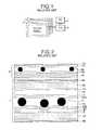
- FIG. 5is a plan view of an exemplary signal line of a touch panel display device according to the present invention.
- FIG. 6is a perspective view of exemplary signal lines of a touch panel display device of FIG. 5 according to the present invention.
- FIG. 5is a plan view of an exemplary signal line of a touch panel display device according to the present invention
- FIG. 6is a perspective view of exemplary signal lines of a touch panel display device of FIG. 5 according to the present invention.
- the touch panel display devicemay include a touch panel 32 having an upper substrate 32 A (in FIG. 6) and a lower substrate 32 B (in FIG. 6) formed of at least one of ITO and PET films, for example, and a spacer (not shown) may be sprayed between the upper and lower substrates 32 A and 32 B.
- the upper and lower substrates 32 A and 32 Bmay be formed by printing silver Ag on a transparent conductive material.
- X-axis electrodes 37 A and 37 Bmay be formed along an edge of the upper substrate 32 A along a vertical direction
- Y-electrodes 36 A and 36 Bmay be formed along an edge of the lower substrate 32 B along a horizontal direction.
- Both the X-axis and Y-axis electrodes 37 A, 37 B, 36 A, and 36 Bmay include a silver material that may be deposited onto the upper and lower substrates 32 A and 32 B, respectively, using a printing process, for example, and a specific voltage may be applied between the X-axis and Y-axis electrodes 37 A, 37 B, 36 A, and 36 B.
- the X-axis electrodes 37 A and 37 Bmay form a first electrode layer, and the Y-axis electrodes 36 A and 36 B may form a second electrode layer.
- the first electrode layer that includes the X-axis electrodes 37 A and 37 Bmay be electrically shorted with the second electrode layer that includes the Y-axis electrodes 36 A and 36 B when a location of the upper substrate 32 A is pressed with a stylus pen or a finger
- the X-axis and Y-axis electrodes 37 A, 37 B, 36 A, and 36 Bmay generate a current and voltage level signal that may change in accordance with the pressed location.
- signal lines 38 A, 38 B, 38 C, and 38 Dmay be electrically connected to the X-axis and Y-axis electrodes 37 A, 37 B, 36 A, and 36 B to supply the current and voltage level signals from the first and the second electrode layers to a touch controller (not shown) to calculate coordinates of the pressed location.
- the signal lines 38 A and 38 Bmay be electrically connected to end portions of the Y-axis electrodes 36 A and 36 B, respectively, and the signal lines 38 C and 38 D may be electrically connected to end portions of the X-axis electrodes 37 A and 37 B, respectively.
- the signal lines 38 A and 38 Bmay be electrically connected to adjacent end portions of the Y-axis electrodes 36 A and 36 B, wherein the signal lines 38 A and 38 B are positioned to extend along a direction parallel to a direction of the Y-axis electrodes 36 A and 36 B.
- the signal lines 38 C and 38 Dmay be electrically connected to adjacent end portions of the X-axis electrodes 37 A and 37 B, wherein the signal lines 38 C and 38 D are positioned to extend along a direction perpendicular to a direction of the X-axis electrodes 37 A and 37 B. Accordingly, as shown in FIG. 5, when the upper and lower substrates 32 A and 32 B are bonded together the signal lines 38 A, 38 B, 38 C, and 38 D are adjacent to each other and extend from the bonded upper and lower substrates 32 A and 32 B along the direction of the Y-axis electrodes 36 A and 36 B. In addition, as shown in FIG.
- the signal lines 38 C and 38 D electrically connected to the X-axis electrodes 37 A and 37 B and the signal lines 38 A and 38 B electrically connected to the Y-axis electrodes 36 A and 36 Bcross over each other.
- the positioning of the signal lines 38 A, 38 B, 38 C, and 38 Dreduces an overall size of the touch panel display device.
Landscapes
- Engineering & Computer Science (AREA)
- General Engineering & Computer Science (AREA)
- Theoretical Computer Science (AREA)
- Physics & Mathematics (AREA)
- General Physics & Mathematics (AREA)
- Human Computer Interaction (AREA)
- Nonlinear Science (AREA)
- Chemical & Material Sciences (AREA)
- Crystallography & Structural Chemistry (AREA)
- Mathematical Physics (AREA)
- Optics & Photonics (AREA)
- Position Input By Displaying (AREA)
- Devices For Indicating Variable Information By Combining Individual Elements (AREA)
- Liquid Crystal (AREA)
Abstract
Description
- The present invention claims the benefit of Korean Patent Application No. P2001-79929 filed in Korea on Dec. 17, 2001, which is hereby incorporated by reference.[0001]
- 1. Field of the Invention[0002]
- The present invention relates to a display device, and more particularly to a signal line of a touch panel display device and method of forming the same.[0003]
- 2. Description of the Related Art[0004]
- In general, a touch panel device is a computer peripheral that is commonly installed on a display surface of an image display device such as a cathode ray tube (CRT), a liquid crystal display (LCD), a field emission display (FED), a plasma display panel (PDP), and an electro-luminescence device (ELD) so that while looking at the image display device, a user applies pressure on the touch panel to enter predetermined information into the computer.[0005]
- FIG. 1 is a perspective view of a touch panel display device and a liquid crystal display panel according to the related art. In FIG. 1, the touch panel display device includes a[0006]
touch panel 2, aliquid crystal panel 1, and abacklight 3. Thetouch panel 2 is electrically connected to acomputer system 5 via atouch controller 4 by signal lines. During operation of the touch panel display device, if a top of thetouch panel 2 is contacted with more than a specific pressure, a voltage value of the contact position is calculated by thetouch controller 4, thereby calculating coordinates of the contact position. - FIG. 2 is a cross sectional view of the touch panel display device and the liquid crystal display panel of FIG. 1 according to the related art. In FIG. 2, a liquid[0007]
crystal display panel 1 is located between an upper polarized sheet4A and a lower polarizedsheet 4B, and thetouch panel 2 is placed on the upper polarized sheet4A. Theliquid crystal panel 1 includesliquid crystal material 14 and aball spacer 5 interposed between alower glass substrate 3A and anupper glass substrate 3B. A gate line6, an insulation film8, a pixel electrode10A, and a first alignment film12A are sequentially formed on thelower glass substrate 3A. Theupper glass substrate 3B has ablack matrix 16, acolor filter 18, acommon electrode 17, and asecond alignment film 12B sequentially formed on a bottom surface thereof. Theball spacer 5 is sprayed on a first alignment film12A before theupper glass substrate 3B is bonded with thelower glass substrate 3A. Theupper glass substrate 3B and thelower glass substrate 3A are separated by theball spacer 5 to be maintained with a specific gap. That is, thespacer 5 uniformly maintains the gap between theupper glass substrate 3B and thelower glass substrate 3A, thereby maintaining a uniform thickness of theliquid crystal material 14. - The[0008]
touch panel 2 includes aspacer 28 formed between alower substrate 20 and anupper substrate 24. Afirst electrode layer 26 is formed on the surface of thelower substrate 20, and asecond electrode layer 27 is formed on a bottom surface of theupper substrate 24. Thesecond electrode layer 27 is electrically shorted with thefirst electrode layer 26 when theupper substrate 24 is pressed with a stylus pen or a finger, to generate a current or voltage level signal that changes in accordance with the pressed position. Accordingly, thefirst electrode layer 26 and thesecond electrode layer 27 are formed by printing silver Ag on transparent conductive material that has good transmittance, and has a low resistance. For example, thefirst electrode layer 26 and thesecond electrode layer 27 include indium-tin-oxide ITO, indium-zinc-oxide IZO, and indium-tin-zinc-oxide ITZO. - FIG. 3 is a plan view of an electrode and a signal line of the touch panel display device of FIG. 2 according to the related art. In FIG. 3, an upper plate of the[0009]
touch panel 2 includesX-axis electrodes signal lines X-axis electrodes touch controller 4. In addition, a lower plate of thetouch panel 2 includes Y-axis electrodes signal lines axis electrode - FIG. 4 is a perspective view of two separate substrates of the touch panel display device of FIG. 3 according to the related art. In FIG. 4, the[0010]
signal lines tail part 29 and an electrode extension connected to theelectrodes electrodes signal lines - However, in the event of extending the[0011]
signal lines touch panel 2, one or more signal lines are formed in the four directions of thetouch panel 2 like A, B, C, and D of FIG. 3. Accordingly, thetouch panel 2 needs a space for the signal lines to be laid besides a display area surrounded by theelectrodes - Accordingly, the present invention is directed to a signal line of a touch panel display device and method of forming the same that substantially obviates one or more of the problems due to limitations and disadvantages of the related art.[0012]
- An object of the present invention is to provide a signal line of a touch panel display device that forms a signal line connected to an electrode of a touch panel using a side portion of the electrode.[0013]
- Another object of the present invention is to provide a method of forming a signal line of a touch panel display device that forms a signal line connected to an electrode of a touch panel using a side portion of the electrode.[0014]
- Additional features and advantages of the invention will be set forth in the description which follows, and in part will be apparent from the description, or may be learned by practice of the invention. The objectives and other advantages of the invention will be realized and attained by the structure particularly pointed out in the written description and claims hereof as well as the appended drawings.[0015]
- To achieve these and other advantages and in accordance with the purpose of the invention, as embodied and broadly described, a signal line of a touch panel display device includes an upper substrate having a first transparent conductive film, a lower substrate having a second transparent conductive film, the lower substrate positioned opposite to the upper substrate, a pair of first electrodes positioned along opposing edges of the upper substrate along a first direction where the first transparent conductive film is formed, a pair of second electrodes positioned along opposing edges of the lower substrate along a second direction perpendicular to the first direction where the second transparent conductive film is formed, and at least one signal line extending from a side portion of one of the pairs of first electrodes and the pairs of second electrodes to a side surface of the touch panel display device to transmit a signal to an external controller.[0016]
- In another aspect, a method of forming a signal line of a touch panel includes forming an upper and a lower substrate of a first material, forming a first transparent conductive film on the upper substrate, forming a second transparent conductive film on the lower substrate, forming a pair of first electrodes along opposing edges of the upper substrate along a first direction where the first transparent conductive film is formed, forming a pair of second electrodes along opposing edges of the lower substrate along a second direction perpendicular to the first direction where the second transparent conductive film is formed, and forming at least one signal line to extend from a side portion of one of the pairs of first and second electrodes to a side surface of the touch panel to transmit a signal to an external controller.[0017]
- It is to be understood that both the foregoing general description and the following detailed description are exemplary and explanatory and are intended to provide further explanation of the invention as claimed.[0018]
- The accompanying drawings, which are included to provide a further understanding of the invention and are incorporated in and constitute a part of this specification, illustrate embodiments of the invention and together with the description serve to explain the principles of the invention. In the drawings:[0019]
- FIG. 1 is a perspective view of a touch panel display device and a liquid crystal display panel according to the related art;[0020]
- FIG. 2 is a cross sectional view of the touch panel display device and the liquid crystal display panel of FIG. 1 according to the related art;[0021]
- FIG. 3 is a plan view of an electrode and a signal line of the touch panel display device of FIG. 2 according to the related art;[0022]
- FIG. 4 is a perspective view of two separate substrates of the touch panel display device of FIG. 3 according to the related art;[0023]
- FIG. 5 is a plan view of an exemplary signal line of a touch panel display device according to the present invention; and[0024]
- FIG. 6 is a perspective view of exemplary signal lines of a touch panel display device of FIG. 5 according to the present invention.[0025]
- Reference will now be made in detail to the preferred embodiments of the present invention, examples of which are illustrated in the accompanying drawings.[0026]
- FIG. 5 is a plan view of an exemplary signal line of a touch panel display device according to the present invention, and FIG. 6 is a perspective view of exemplary signal lines of a touch panel display device of FIG. 5 according to the present invention. In FIG. 5, the touch panel display device may include a[0027]
touch panel 32 having anupper substrate 32A (in FIG. 6) and alower substrate 32B (in FIG. 6) formed of at least one of ITO and PET films, for example, and a spacer (not shown) may be sprayed between the upper andlower substrates lower substrates - In FIG. 5,[0028]
X-axis electrodes upper substrate 32A along a vertical direction, and Y-electrodes lower substrate 32B along a horizontal direction. Both the X-axis and Y-axis electrodes lower substrates axis electrodes X-axis electrodes axis electrodes X-axis electrodes axis electrodes upper substrate 32A is pressed with a stylus pen or a finger, the X-axis and Y-axis electrodes signal lines axis electrodes - In FIG. 6, the[0029]
signal lines axis electrodes signal lines X-axis electrodes signal lines axis electrodes signal lines axis electrodes signal lines X-axis electrodes signal lines X-axis electrodes lower substrates signal lines lower substrates axis electrodes signal lines X-axis electrodes signal lines axis electrodes signal lines - It will be apparent to those skilled in the art that various modification and variations can be made in the signal line of a touch panel display device and a method of forming a signal line of a touch panel display device of the present invention without departing from the spirit or scope of the invention. Thus, it is intended that the present invention cover the modifications and variations provided they come within the scope of the appended claims and their equivalents.[0030]
Claims (10)
Applications Claiming Priority (2)
| Application Number | Priority Date | Filing Date | Title |
|---|---|---|---|
| KR10-2001-0079929AKR100487356B1 (en) | 2001-12-17 | 2001-12-17 | Method of forming signal line of touch panel |
| KRP2001-79929 | 2001-12-17 |
Publications (2)
| Publication Number | Publication Date |
|---|---|
| US20030112227A1true US20030112227A1 (en) | 2003-06-19 |
| US7050047B2 US7050047B2 (en) | 2006-05-23 |
Family
ID=19717115
Family Applications (1)
| Application Number | Title | Priority Date | Filing Date |
|---|---|---|---|
| US10/319,632Expired - LifetimeUS7050047B2 (en) | 2001-12-17 | 2002-12-16 | Signal line of touch panel display device and method of forming the same |
Country Status (5)
| Country | Link |
|---|---|
| US (1) | US7050047B2 (en) |
| JP (1) | JP4546025B2 (en) |
| KR (1) | KR100487356B1 (en) |
| CN (1) | CN1326031C (en) |
| DE (1) | DE10258450B4 (en) |
Cited By (10)
| Publication number | Priority date | Publication date | Assignee | Title |
|---|---|---|---|---|
| US20030122800A1 (en)* | 2001-12-27 | 2003-07-03 | Lg, Philips Lcd Co., Ltd. | Touch panel liquid crystal display device and method of fabricating the same |
| US20030122797A1 (en)* | 2001-12-27 | 2003-07-03 | Lg.Philips Lcd Co., Ltd. | Touch panel display device and method of fabricating the same |
| US20050280634A1 (en)* | 2004-06-21 | 2005-12-22 | Matsushita Electric Industrial Co., Ltd. | Input panel and input device using the panel |
| US20080259037A1 (en)* | 2007-04-19 | 2008-10-23 | Samsung Sdi Co., Ltd. | Multifunction key pad display and electronic device having the same |
| US20080284737A1 (en)* | 2007-04-19 | 2008-11-20 | Samsung Sdi Co., Ltd. | Display for a keypad and electronic device having the same |
| US20090213089A1 (en)* | 2008-02-21 | 2009-08-27 | Min Woo Hwang | Flat display device unified with touch panel |
| KR101121906B1 (en) | 2003-12-30 | 2012-03-19 | 쓰리엠 이노베이티브 프로퍼티즈 컴파니 | Touch sensor with linearized response |
| CN108271417A (en)* | 2016-11-04 | 2018-07-10 | 京东方科技集团股份有限公司 | Touch base plate, touch panel, touch control display apparatus, mask plate, manufacturing method |
| US10444929B2 (en)* | 2016-09-09 | 2019-10-15 | Boe Technology Group Co., Ltd. | Laser touch panel, display device, display system and laser touch method |
| US20230077382A1 (en)* | 2020-02-25 | 2023-03-16 | Peratech Holdco Limited | Pressure sensor |
Families Citing this family (14)
| Publication number | Priority date | Publication date | Assignee | Title |
|---|---|---|---|---|
| KR100459231B1 (en)* | 2002-11-15 | 2004-12-03 | 엘지.필립스 엘시디 주식회사 | Touch panel |
| JP2006031207A (en)* | 2004-07-14 | 2006-02-02 | Fujitsu Ltd | Panel unit, display device, and electronic device |
| CN100379056C (en)* | 2005-03-01 | 2008-04-02 | 友达光电股份有限公司 | Flat panel display with touch control function and forming method thereof |
| CN101078961B (en)* | 2006-05-27 | 2011-04-06 | 智点科技(深圳)有限公司 | Line surface electrode type touch-control screen |
| CN101192258B (en)* | 2006-11-20 | 2012-03-07 | 鸿富锦精密工业(深圳)有限公司 | Electronic device and method for opening same |
| CN101192260B (en)* | 2006-11-24 | 2012-08-22 | 鸿富锦精密工业(深圳)有限公司 | Electronic device and method for opening same |
| US7755488B2 (en)* | 2007-09-21 | 2010-07-13 | Baxter International Inc. | Access disconnection detection system |
| US8221320B2 (en) | 2007-09-21 | 2012-07-17 | Baxter International Inc. | Access disconnect detection system |
| CN101526864B (en)* | 2008-03-04 | 2012-01-11 | 胜华科技股份有限公司 | Touch panel |
| US8114043B2 (en) | 2008-07-25 | 2012-02-14 | Baxter International Inc. | Electromagnetic induction access disconnect sensor |
| JP2012221120A (en)* | 2011-04-06 | 2012-11-12 | Fujitsu Component Ltd | Touch panel |
| WO2013056438A1 (en)* | 2011-10-19 | 2013-04-25 | Tpk Touch Solutions Inc. | Touch sensitive display |
| KR102075921B1 (en)* | 2013-04-29 | 2020-02-11 | 엘지디스플레이 주식회사 | Anti-static electricity layer and method for manufacturing of the same, display device comprising the same |
| EP3724717A4 (en)* | 2017-12-13 | 2021-07-21 | Boe Technology Group Co., Ltd. | Display apparatus having transparent magnetic layer, and fabricating method thereof |
Citations (9)
| Publication number | Priority date | Publication date | Assignee | Title |
|---|---|---|---|---|
| US5062198A (en)* | 1990-05-08 | 1991-11-05 | Keytec, Inc. | Method of making a transparent touch screen switch assembly |
| US5228562A (en)* | 1991-09-09 | 1993-07-20 | Gm Nameplate, Inc. | Membrane switch and fabrication method |
| US5518078A (en)* | 1991-11-08 | 1996-05-21 | Sharp Kabushiki Kaisha | Coordinates input device |
| US5854881A (en)* | 1994-05-31 | 1998-12-29 | Sharp Kabushiki Kaisha | Coordinate detection device capable of detecting coordinates using display panel provided specially for display |
| US20020000979A1 (en)* | 2000-06-28 | 2002-01-03 | Shoji Furuhashi | Touch panel, method for manufacturing the same, and screen input type display unit using the same |
| US6380497B1 (en)* | 1997-10-09 | 2002-04-30 | Nissha Printing Co., Ltd. | High strength touch panel and method of manufacturing the same |
| US6433841B1 (en)* | 1997-12-19 | 2002-08-13 | Seiko Epson Corporation | Electro-optical apparatus having faces holding electro-optical material in between flattened by using concave recess, manufacturing method thereof, and electronic device using same |
| US20030043122A1 (en)* | 2000-03-06 | 2003-03-06 | Hitachi, Ltd. | Touch panel and screen input type liquid crystal display device |
| US6541913B1 (en)* | 1999-07-02 | 2003-04-01 | Sony Corporation | Flat display apparatus |
Family Cites Families (7)
| Publication number | Priority date | Publication date | Assignee | Title |
|---|---|---|---|---|
| JPH04209430A (en)* | 1990-08-23 | 1992-07-30 | Nitto Denko Corp | Touch panel and its manufacturing method |
| US5329291A (en)* | 1993-08-18 | 1994-07-12 | Liang Ying Co., Ltd. | Cathode ray tube optical filter device with cursor pointing function |
| JP3825487B2 (en) | 1995-03-03 | 2006-09-27 | 日本写真印刷株式会社 | Transparent touch panel |
| JPH08328742A (en)* | 1995-06-05 | 1996-12-13 | Hitachi Ltd | Touch panel control method and coordinate input device |
| JP3532378B2 (en)* | 1997-04-08 | 2004-05-31 | 日本写真印刷株式会社 | Touch panel |
| JPH11219259A (en)* | 1998-02-03 | 1999-08-10 | Gunze Ltd | Resistance film type touch panel |
| KR100375175B1 (en)* | 2001-01-10 | 2003-03-06 | 주식회사 에이터치 | A Contact Structure of Touch Panel |
- 2001
- 2001-12-17KRKR10-2001-0079929Apatent/KR100487356B1/ennot_activeExpired - Lifetime
- 2002
- 2002-12-13DEDE10258450.8Apatent/DE10258450B4/ennot_activeExpired - Lifetime
- 2002-12-16USUS10/319,632patent/US7050047B2/ennot_activeExpired - Lifetime
- 2002-12-17JPJP2002365432Apatent/JP4546025B2/ennot_activeExpired - Lifetime
- 2002-12-17CNCNB021566577Apatent/CN1326031C/ennot_activeExpired - Lifetime
Patent Citations (9)
| Publication number | Priority date | Publication date | Assignee | Title |
|---|---|---|---|---|
| US5062198A (en)* | 1990-05-08 | 1991-11-05 | Keytec, Inc. | Method of making a transparent touch screen switch assembly |
| US5228562A (en)* | 1991-09-09 | 1993-07-20 | Gm Nameplate, Inc. | Membrane switch and fabrication method |
| US5518078A (en)* | 1991-11-08 | 1996-05-21 | Sharp Kabushiki Kaisha | Coordinates input device |
| US5854881A (en)* | 1994-05-31 | 1998-12-29 | Sharp Kabushiki Kaisha | Coordinate detection device capable of detecting coordinates using display panel provided specially for display |
| US6380497B1 (en)* | 1997-10-09 | 2002-04-30 | Nissha Printing Co., Ltd. | High strength touch panel and method of manufacturing the same |
| US6433841B1 (en)* | 1997-12-19 | 2002-08-13 | Seiko Epson Corporation | Electro-optical apparatus having faces holding electro-optical material in between flattened by using concave recess, manufacturing method thereof, and electronic device using same |
| US6541913B1 (en)* | 1999-07-02 | 2003-04-01 | Sony Corporation | Flat display apparatus |
| US20030043122A1 (en)* | 2000-03-06 | 2003-03-06 | Hitachi, Ltd. | Touch panel and screen input type liquid crystal display device |
| US20020000979A1 (en)* | 2000-06-28 | 2002-01-03 | Shoji Furuhashi | Touch panel, method for manufacturing the same, and screen input type display unit using the same |
Cited By (18)
| Publication number | Priority date | Publication date | Assignee | Title |
|---|---|---|---|---|
| US20030122797A1 (en)* | 2001-12-27 | 2003-07-03 | Lg.Philips Lcd Co., Ltd. | Touch panel display device and method of fabricating the same |
| US6914640B2 (en)* | 2001-12-27 | 2005-07-05 | Lg. Philips Lcd Co., Ltd. | Touch panel liquid crystal display device and method of fabricating the same |
| US8514182B2 (en)* | 2001-12-27 | 2013-08-20 | Lg Display Co., Ltd. | Touch panel display device and method of fabricating the same |
| US20030122800A1 (en)* | 2001-12-27 | 2003-07-03 | Lg, Philips Lcd Co., Ltd. | Touch panel liquid crystal display device and method of fabricating the same |
| KR101121906B1 (en) | 2003-12-30 | 2012-03-19 | 쓰리엠 이노베이티브 프로퍼티즈 컴파니 | Touch sensor with linearized response |
| US20050280634A1 (en)* | 2004-06-21 | 2005-12-22 | Matsushita Electric Industrial Co., Ltd. | Input panel and input device using the panel |
| US8330724B2 (en) | 2007-04-19 | 2012-12-11 | Samsung Display Co., Ltd. | Multifunction key pad display and electronic device having the same |
| US20080259037A1 (en)* | 2007-04-19 | 2008-10-23 | Samsung Sdi Co., Ltd. | Multifunction key pad display and electronic device having the same |
| US20080284737A1 (en)* | 2007-04-19 | 2008-11-20 | Samsung Sdi Co., Ltd. | Display for a keypad and electronic device having the same |
| US8259070B2 (en) | 2007-04-19 | 2012-09-04 | Samsung Mobile Display Co., Ltd. | Display for a keypad and electronic device having the same |
| US8179379B2 (en)* | 2008-02-21 | 2012-05-15 | Lg Display Co. Ltd. | Flat display device unified with touch panel |
| US20090213089A1 (en)* | 2008-02-21 | 2009-08-27 | Min Woo Hwang | Flat display device unified with touch panel |
| US10444929B2 (en)* | 2016-09-09 | 2019-10-15 | Boe Technology Group Co., Ltd. | Laser touch panel, display device, display system and laser touch method |
| CN108271417A (en)* | 2016-11-04 | 2018-07-10 | 京东方科技集团股份有限公司 | Touch base plate, touch panel, touch control display apparatus, mask plate, manufacturing method |
| US10365776B2 (en)* | 2016-11-04 | 2019-07-30 | Boe Technology Group Co., Ltd. | Touch substrate, touch panel, touch display apparatus, mask plate, and fabricating method |
| US10572091B2 (en) | 2016-11-04 | 2020-02-25 | Boe Technology Group Co., Ltd. | Touch substrate, touch panel, touch display apparatus, mask plate, and fabricating method |
| US20230077382A1 (en)* | 2020-02-25 | 2023-03-16 | Peratech Holdco Limited | Pressure sensor |
| US11868554B2 (en)* | 2020-02-25 | 2024-01-09 | Peratech Holdco Limited | Pressure sensor |
Also Published As
| Publication number | Publication date |
|---|---|
| KR20030049647A (en) | 2003-06-25 |
| CN1427330A (en) | 2003-07-02 |
| DE10258450B4 (en) | 2015-04-09 |
| JP2003241899A (en) | 2003-08-29 |
| DE10258450A1 (en) | 2003-07-03 |
| JP4546025B2 (en) | 2010-09-15 |
| US7050047B2 (en) | 2006-05-23 |
| KR100487356B1 (en) | 2005-05-03 |
| CN1326031C (en) | 2007-07-11 |
Similar Documents
| Publication | Publication Date | Title |
|---|---|---|
| US7050047B2 (en) | Signal line of touch panel display device and method of forming the same | |
| US7336261B2 (en) | Touch panel display apparatus and method of fabricating the same | |
| US9164306B2 (en) | In-cell touch display panel system using metal wires to connect with sensing electrodes | |
| US8390575B2 (en) | Touch-sensitive liquid crystal display panel with built-in touch mechanism and method for driving same | |
| US9007329B2 (en) | Liquid crystal display device including touch panel | |
| US6914640B2 (en) | Touch panel liquid crystal display device and method of fabricating the same | |
| US6972750B2 (en) | Liquid crystal panel device having a touch panel and method of fabricating the same | |
| US8736576B2 (en) | Display device having touch panel | |
| US20080100590A1 (en) | Display device | |
| US20040095335A1 (en) | Touch panel for display device | |
| JP2008134975A (en) | Input device and its manufacturing method | |
| US20040041796A1 (en) | Touch panel device and method of fabricating the same | |
| US9019221B2 (en) | Display device integrated with touch screen panel | |
| US8514182B2 (en) | Touch panel display device and method of fabricating the same | |
| US9753572B2 (en) | Touch panel, method of fabricating the same and touch display device | |
| KR101859469B1 (en) | Display device and manufacturing method thereof | |
| JP2015099407A (en) | Input device | |
| KR20030055990A (en) | Display device associated with touch panel | |
| KR100891495B1 (en) | Touch panel integrated display device | |
| KR100475723B1 (en) | Touch Panel Integrated Liquid Crystal Panel and Fabricated Method Thereof | |
| KR100539582B1 (en) | Touch panel and method for fabricating the same | |
| KR20120063355A (en) | Display device associated with touch panel and manufacturing method thereof | |
| KR100472362B1 (en) | Method of formating signal line of touch panel | |
| KR200226352Y1 (en) | Icon unity type Touch panel |
Legal Events
| Date | Code | Title | Description |
|---|---|---|---|
| AS | Assignment | Owner name:LG.PHILIPS LCD CO., LTD., KOREA, REPUBLIC OF Free format text:ASSIGNMENT OF ASSIGNORS INTEREST;ASSIGNOR:HONG, HEE JUNG;REEL/FRAME:013703/0576 Effective date:20030124 | |
| FEPP | Fee payment procedure | Free format text:PAYOR NUMBER ASSIGNED (ORIGINAL EVENT CODE: ASPN); ENTITY STATUS OF PATENT OWNER: LARGE ENTITY Free format text:PAYER NUMBER DE-ASSIGNED (ORIGINAL EVENT CODE: RMPN); ENTITY STATUS OF PATENT OWNER: LARGE ENTITY | |
| STCF | Information on status: patent grant | Free format text:PATENTED CASE | |
| AS | Assignment | Owner name:LG DISPLAY CO., LTD., KOREA, REPUBLIC OF Free format text:CHANGE OF NAME;ASSIGNOR:LG.PHILIPS LCD CO., LTD.;REEL/FRAME:021754/0230 Effective date:20080304 Owner name:LG DISPLAY CO., LTD.,KOREA, REPUBLIC OF Free format text:CHANGE OF NAME;ASSIGNOR:LG.PHILIPS LCD CO., LTD.;REEL/FRAME:021754/0230 Effective date:20080304 | |
| FPAY | Fee payment | Year of fee payment:4 | |
| FEPP | Fee payment procedure | Free format text:PAYOR NUMBER ASSIGNED (ORIGINAL EVENT CODE: ASPN); ENTITY STATUS OF PATENT OWNER: LARGE ENTITY Free format text:PAYER NUMBER DE-ASSIGNED (ORIGINAL EVENT CODE: RMPN); ENTITY STATUS OF PATENT OWNER: LARGE ENTITY | |
| FPAY | Fee payment | Year of fee payment:8 | |
| MAFP | Maintenance fee payment | Free format text:PAYMENT OF MAINTENANCE FEE, 12TH YEAR, LARGE ENTITY (ORIGINAL EVENT CODE: M1553) Year of fee payment:12 |