US20030111736A1 - Csp chip stack with flex circuit - Google Patents
Csp chip stack with flex circuitDownload PDFInfo
- Publication number
- US20030111736A1 US20030111736A1US10/016,939US1693901AUS2003111736A1US 20030111736 A1US20030111736 A1US 20030111736A1US 1693901 AUS1693901 AUS 1693901AUS 2003111736 A1US2003111736 A1US 2003111736A1
- Authority
- US
- United States
- Prior art keywords
- flex
- integrated circuit
- circuit chip
- flex substrate
- chip stack
- Prior art date
- Legal status (The legal status is an assumption and is not a legal conclusion. Google has not performed a legal analysis and makes no representation as to the accuracy of the status listed.)
- Granted
Links
Images

Classifications
- H—ELECTRICITY
- H01—ELECTRIC ELEMENTS
- H01L—SEMICONDUCTOR DEVICES NOT COVERED BY CLASS H10
- H01L23/00—Details of semiconductor or other solid state devices
- H01L23/52—Arrangements for conducting electric current within the device in operation from one component to another, i.e. interconnections, e.g. wires, lead frames
- H01L23/538—Arrangements for conducting electric current within the device in operation from one component to another, i.e. interconnections, e.g. wires, lead frames the interconnection structure between a plurality of semiconductor chips being formed on, or in, insulating substrates
- H01L23/5387—Flexible insulating substrates
- H—ELECTRICITY
- H01—ELECTRIC ELEMENTS
- H01L—SEMICONDUCTOR DEVICES NOT COVERED BY CLASS H10
- H01L25/00—Assemblies consisting of a plurality of semiconductor or other solid state devices
- H01L25/03—Assemblies consisting of a plurality of semiconductor or other solid state devices all the devices being of a type provided for in a single subclass of subclasses H10B, H10D, H10F, H10H, H10K or H10N, e.g. assemblies of rectifier diodes
- H01L25/10—Assemblies consisting of a plurality of semiconductor or other solid state devices all the devices being of a type provided for in a single subclass of subclasses H10B, H10D, H10F, H10H, H10K or H10N, e.g. assemblies of rectifier diodes the devices having separate containers
- H01L25/105—Assemblies consisting of a plurality of semiconductor or other solid state devices all the devices being of a type provided for in a single subclass of subclasses H10B, H10D, H10F, H10H, H10K or H10N, e.g. assemblies of rectifier diodes the devices having separate containers the devices being integrated devices of class H10
- H—ELECTRICITY
- H01—ELECTRIC ELEMENTS
- H01L—SEMICONDUCTOR DEVICES NOT COVERED BY CLASS H10
- H01L2225/00—Details relating to assemblies covered by the group H01L25/00 but not provided for in its subgroups
- H01L2225/03—All the devices being of a type provided for in the same main group of the same subclass of class H10, e.g. assemblies of rectifier diodes
- H01L2225/04—All the devices being of a type provided for in the same main group of the same subclass of class H10, e.g. assemblies of rectifier diodes the devices not having separate containers
- H01L2225/065—All the devices being of a type provided for in the same main group of the same subclass of class H10
- H01L2225/06503—Stacked arrangements of devices
- H01L2225/06517—Bump or bump-like direct electrical connections from device to substrate
- H—ELECTRICITY
- H01—ELECTRIC ELEMENTS
- H01L—SEMICONDUCTOR DEVICES NOT COVERED BY CLASS H10
- H01L2225/00—Details relating to assemblies covered by the group H01L25/00 but not provided for in its subgroups
- H01L2225/03—All the devices being of a type provided for in the same main group of the same subclass of class H10, e.g. assemblies of rectifier diodes
- H01L2225/04—All the devices being of a type provided for in the same main group of the same subclass of class H10, e.g. assemblies of rectifier diodes the devices not having separate containers
- H01L2225/065—All the devices being of a type provided for in the same main group of the same subclass of class H10
- H01L2225/06503—Stacked arrangements of devices
- H01L2225/06551—Conductive connections on the side of the device
- H—ELECTRICITY
- H01—ELECTRIC ELEMENTS
- H01L—SEMICONDUCTOR DEVICES NOT COVERED BY CLASS H10
- H01L2225/00—Details relating to assemblies covered by the group H01L25/00 but not provided for in its subgroups
- H01L2225/03—All the devices being of a type provided for in the same main group of the same subclass of class H10, e.g. assemblies of rectifier diodes
- H01L2225/04—All the devices being of a type provided for in the same main group of the same subclass of class H10, e.g. assemblies of rectifier diodes the devices not having separate containers
- H01L2225/065—All the devices being of a type provided for in the same main group of the same subclass of class H10
- H01L2225/06503—Stacked arrangements of devices
- H01L2225/06579—TAB carriers; beam leads
- H—ELECTRICITY
- H01—ELECTRIC ELEMENTS
- H01L—SEMICONDUCTOR DEVICES NOT COVERED BY CLASS H10
- H01L2225/00—Details relating to assemblies covered by the group H01L25/00 but not provided for in its subgroups
- H01L2225/03—All the devices being of a type provided for in the same main group of the same subclass of class H10, e.g. assemblies of rectifier diodes
- H01L2225/10—All the devices being of a type provided for in the same main group of the same subclass of class H10, e.g. assemblies of rectifier diodes the devices having separate containers
- H01L2225/1005—All the devices being of a type provided for in the same main group of the same subclass of class H10, e.g. assemblies of rectifier diodes the devices having separate containers the devices being integrated devices of class H10
- H01L2225/1011—All the devices being of a type provided for in the same main group of the same subclass of class H10, e.g. assemblies of rectifier diodes the devices having separate containers the devices being integrated devices of class H10 the containers being in a stacked arrangement
- H01L2225/1047—Details of electrical connections between containers
- H01L2225/1058—Bump or bump-like electrical connections, e.g. balls, pillars, posts
- H—ELECTRICITY
- H01—ELECTRIC ELEMENTS
- H01L—SEMICONDUCTOR DEVICES NOT COVERED BY CLASS H10
- H01L2225/00—Details relating to assemblies covered by the group H01L25/00 but not provided for in its subgroups
- H01L2225/03—All the devices being of a type provided for in the same main group of the same subclass of class H10, e.g. assemblies of rectifier diodes
- H01L2225/10—All the devices being of a type provided for in the same main group of the same subclass of class H10, e.g. assemblies of rectifier diodes the devices having separate containers
- H01L2225/1005—All the devices being of a type provided for in the same main group of the same subclass of class H10, e.g. assemblies of rectifier diodes the devices having separate containers the devices being integrated devices of class H10
- H01L2225/1011—All the devices being of a type provided for in the same main group of the same subclass of class H10, e.g. assemblies of rectifier diodes the devices having separate containers the devices being integrated devices of class H10 the containers being in a stacked arrangement
- H01L2225/1047—Details of electrical connections between containers
- H01L2225/107—Indirect electrical connections, e.g. via an interposer, a flexible substrate, using TAB
- H—ELECTRICITY
- H01—ELECTRIC ELEMENTS
- H01L—SEMICONDUCTOR DEVICES NOT COVERED BY CLASS H10
- H01L2924/00—Indexing scheme for arrangements or methods for connecting or disconnecting semiconductor or solid-state bodies as covered by H01L24/00
- H01L2924/0001—Technical content checked by a classifier
- H01L2924/0002—Not covered by any one of groups H01L24/00, H01L24/00 and H01L2224/00
Definitions
- the present inventionrelates generally to chip stacks, and more particularly to a chip stack having connections routed from the bottom to the perimeter thereof to allow multiple integrated circuit chips such as CSP devices to be quickly, easily and inexpensively vertically interconnected in a volumetrically efficient manner.
- Z-Stackingperhaps one of the most commonly used techniques to increase memory capacity is the stacking of memory devices into a vertical chip stack, sometimes referred to as 3D packaging or Z-Stacking.
- Z-Stackingfrom two (2) to as many as eight (8) memory devices or other integrated circuit (IC) chips are interconnected in a single component (i.e., chip stack) which is mountable to the “footprint” typically used for a single package device such as a packaged chip.
- TSOPthin small outline package
- LCCleadless chip carrier
- the various arrangements and techniques described in these issued patents and other currently pending patent applications of Applicanthave been found to provide chip stacks which are relatively easy and inexpensive to manufacture, and are well suited for use in a multitude of differing applications.
- the present inventionprovides yet a further alternative arrangement and technique for forming a volumetrically efficient chip stack.
- connectionsare routed from the bottom of the chip stack to the perimeter thereof so that interconnections can be made vertically which allows multiple integrated circuit chips such as BGA, CSP, fine pitch BGA, or flip chip devices to be stacked in a manner providing the potential for significant increases in the production rate of the chip stack and resultant reductions in the cost thereof.
- a chip stackcomprising a flex circuit.
- the flex circuititself comprises a flex substrate having a first conductive pattern disposed thereon, and a plurality of leads extending therefrom.
- the leads of the flex circuitare electrically connected to the first conductive pattern thereof.
- the chip stackcomprises at least two integrated circuit chip packages which are electrically connected to the first conductive pattern.
- the first conductive patterncomprises first and second sets of flex pads which are disposed on respective ones of the opposed top and bottom surfaces of the flex substrate, with one of the integrated circuit chip packages being disposed on the top surface of the flex substrate and electrically connected to at least some of the flex pads of the first set, and one of the integrated circuit chips being disposed upon the bottom surface of the flex substrate and electrically connected to at least some of the flex pads of the second set.
- the integrated circuit chip packagesmay each comprise a CSP device.
- a chip stackcomprising a flex circuit.
- the flex circuititself comprises a flex substrate having a first conductive pattern disposed thereon, and a plurality of conductive leads extending therefrom.
- the leads of the flex circuitare electrically connected to the first conductive pattern thereon.
- the chip stackfurther comprises at least two integrated circuit chip packages, one of which is electrically connected to the first conductive pattern, with the remaining integrated circuit chip package being in non-conductive attachment to the flex substrate.
- the first conductive pattern of the flex circuitcomprises a first set of flex pads disposed on the top surface of the flex substrate and electrically connected to respective ones of the leads.
- One of the integrated circuit chip packagesis disposed upon the top surface of the flex substrate and electrically connected to at least some of the flex pads of the first set, with the remaining integrated circuit chip package being attached to the bottom surface of the flex substrate.
- the conductive contacts of the integrated circuit chip package attached to the bottom surface of the flex substrate and the leads of the flex circuitcollectively define a composite footprint of the chip stack which is electrically connectable to another component.
- the leads of the chip stackmay each comprise either an S-lead or a J-lead.
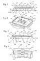
- FIG. 1is a side-elevational view of a chip stack constructed in accordance with a first embodiment of the present invention
- FIG. 2is a top perspective view of the flex circuit included in the chip stack shown in FIG. 1;
- FIG. 3is a side-elevational view of a chip stack constructed in accordance with a second embodiment of the present invention.
- FIG. 4is a side-elevational view of a chip stack constructed in accordance with a third embodiment of the present invention.
- FIG. 1depicts a chip stack 10 constructed in accordance with a first embodiment of the present invention.
- the chip stack 10comprises a flex circuit 12 .
- the flex circuit 12itself comprises a rectangularly configured flex substrate 14 which defines a generally planar top surface 16 , a generally planar bottom surface 18 , an opposed pair of longitudinal peripheral edge segments 20 , and an opposed pair of lateral peripheral edge segments 22 .
- the first conductive patternitself preferably comprises a first set of flex pads 24 which are disposed on the top surface 16 of the flex substrate 14 , and a second set of flex pads 25 which are disposed on the bottom surface 18 of the flex substrate 14 .
- the flex pads 24 of the first setare arranged in a generally rectangular pattern or array in the central portion of the top surface 16 .
- the flex pads 25 of the second setare arranged in a generally rectangular pattern or array in the central portion of the bottom surface 18 .
- the flex pads 24 of the first set and the flex pads 25 of the second setwill be arranged in identical patterns, with each of the flex pads 24 of the first set being coaxially aligned with a respective one of the flex pads 25 of the second set.
- the flex pads 24 of the first set and the flex pads 25 of the second setmay be disposed upon the flex substrate 14 in dissimilar patterns.
- the flex substrate 14is described as being rectangularly configured, it will be recognized that the same may be formed in alternative shapes (e.g., square).
- the leads 26each comprise an S-lead (i.e., gull wing) having the general shape of the letter S.
- S-leadi.e., gull wing
- Each of the leads 26are electrically connected to the first conductive pattern and, in particular, to the flex pads 24 , 25 of the first and second sets.
- the first conductive pattern of the flex circuit 12may be configured such that the flex pads 24 of the first set and the flex pads 25 of the second set are each electrically connected to respective ones of the leads 26 .
- first conductive patternmay include conductive traces which extend within the flex substrate 14 in any pattern or arrangement as is needed to achieve a desired signal routing.
- Any flex pad 24 of the first setmay be electrically connected to the flex pad 25 of the second set coaxially aligned therewith by a via or feed-through hole extending through the flex substrate 14 therebetween.
- the flex pads 24 of the first set, the flex pads 25 of the second set, and the conductive traces extending within the flex substrate 14are each preferably fabricated from very thin copper having a thickness in the range of from about five microns to about twenty-five microns through the use of conventional etching techniques.
- the use of thin copper for the various pads and tracesallows for etching line widths and spacings down to a pitch of about four mils which substantially increases the routing density of the flex circuit 12 .
- the flex substrate 14is preferably fabricated from either FR-4, a polyimide film, or some other suitable material which can easily be routed.
- the material used to form the flex substrate 14may be as thin as about fifty microns or may be a thicker multi-layer structure.
- the chip stack 10further comprises at least two identically configured integrated circuit chip packages 28 .
- Each of the integrated circuit chip packages 28comprises a rectangularly configured package body 30 defining a generally planar top surface 32 , a generally planar bottom surface 34 , an opposed pair of longitudinal sides, and an opposed pair of lateral sides.
- Disposed on the bottom surface 34 of the package body 30are a plurality of spherically or semi-spherically shaped conductive contacts 36 which are preferably arranged in a pattern identical to the patterns of the flex pads 24 of the first set and the flex pads 25 of the second set.
- the conductive contacts 36 of one of the integrated circuit chip packages 28are electrically connected to respective ones of the flex pads 24 of the first set, with the conductive contacts 36 of the remaining integrated circuit chip package 28 being electrically connected to respective ones of the flex pads 25 of the second set. Such electrical connection is preferably accomplished via soldering.
- Each of the integrated circuit chip packages 28is preferably a CSP (chip scale package) device such as a BGA (ball grid array) device, a fine pitch BGA device, or a flip chip device.
- the integrated circuit chip packages 28are electrically connected to the first conductive pattern of the flex circuit 12 in the above-described manner.
- a layer 38 of flux/underfill materialmay optionally be applied between the bottom surfaces 34 of the package bodies 30 and respective ones of the top and bottom surfaces 16 , 18 of the flex substrate 14 .
- the leads 26are sized relative to the integrated circuit chip packages 28 such that the outwardly turned distal end of each lead 26 extends beyond the top surface 32 of the lowermost integrated circuit chip package 28 of the chip stack 10 (i.e., the integrated circuit chip package 28 disposed on the bottom surface 18 and electrically connected to the flex pads 25 of the second set).
- the number and orientation/pattern of leads 26 extending from the flex substrate 14is dependent upon the desired “footprint” of the chip stack 10 .
- the leads 26may protrude from each of the longitudinal and lateral peripheral edge segments 20 , 22 of the flex substrate 14 .
- the leads 28may extend from only each of the longitudinal peripheral edge segments 20 , or each of the lateral peripheral edge segments 22 .
- the leads 26may extend from one longitudinal peripheral edge segment 20 and/or one lateral peripheral edge segment 22 .
- the leads 26need not necessarily be provided in a continuous row along any longitudinal or lateral peripheral edge segment 20 , 22 of the flex substrate 14 .
- the chip stack 100comprises a flex circuit 112 which is identical to the flex circuit 12 of the chip stack 10 in almost all respects, except that the flex circuit 112 of the chip stack 100 does not include the second set of flex pads 25 described above.
- the first conductive pattern of the flex circuit 112comprises only the first set of flex pads 224 disposed in a generally rectangular pattern or array in the central portion of the top surface 116 of the flex substrate 114 .
- the leads 126 thereofare electrically connected to respective ones of the flex pads 224 of the first set via conductive traces which extend within the flex substrate 114 . It is contemplated that the conductive traces may be arranged in a pattern such that two or more of the flex pads 224 of the first set may be electrically connected to a single lead 126 .
- the chip stack 100 of the second embodimentfurther comprises two identically configured integrated circuit chip packages 128 which are identical to the integrated circuit chip packages 28 of the chip stack 10 , and each preferably comprises a rectangularly configured package body 130 having a plurality of conductive contacts 136 disposed on the bottom surface 134 thereof.
- each of the integrated circuit chip packages 128preferably comprises a CSP device such as a BGA device, a fine pitch BGA device, or a flip chip device.
- one of the integrated circuit chip packages 128is electrically connected to the first conductive pattern of the flex circuit 112 . More particularly, the conductive contacts 136 of one of the integrated circuit chip packages 128 are electrically connected to respective ones of the flex pads 224 of the first set. The conductive contacts 136 and flex pads 124 are preferably arranged in identical patterns. The remaining integrated circuit chip package 128 in the chip stack 100 (i.e., the lowermost integrated circuit chip package 128 in the chip stack 100 ) is attached to the bottom surface 118 of the flex substrate 114 of the flex circuit 112 .
- the top surface 132 of the package body 130 of the lowermost integrated circuit chip package 128is rigidly affixed to the bottom surface 118 via an adhesive layer 142 .
- the leads 126 of the flex circuit 112 and integrated circuit chip packages 128are preferably sized relative to each other such that the outwardly turned distal ends of the leads 126 and the conductive contacts 136 of the lowermost integrated circuit chip package 128 (which is adhesively affixed to the bottom surface 118 of the flex substrate 114 ) extend in substantially coplanar relation to each other.
- the leads 126 and conductive contacts 136collectively define a composite footprint (ball and lead) for the chip stack 100 which is electrically connectable to an underlying component such as a printed circuit board 140 .
- the chip stack 100 of the second embodimentis preferably assembled by initially electrically connecting one of the integrated circuit chip packages 128 to the first conductive pattern of the flex circuit 112 in the above-described manner. Thereafter, the remaining integrated circuit chip package 128 is secured to the bottom surface 118 of the flex substrate 114 in the above-described manner.
- a layer 138 of flux/underfill materialmay be applied between the bottom surface 134 of the uppermost integrated circuit chip package 128 and the top surface 116 of the flex substrate 114 of the flex circuit 112 .
- FIG. 4there is depicted a chip stack 200 constructed in accordance with a third embodiment of the present invention.
- the chip stack 200 of the third embodimentis virtually identical to the chip stack 100 of the second embodiment, with the exception that the leads 238 of the flex circuit 212 of the chip stack 200 , each comprise a J-lead having a generally J shape as opposed to the S-leads shown and described in relation to the flex circuit 112 .
- the leads 238 and integrated circuit chip packages 228are sized and configured relative to each other such that the inwardly turned distal ends of the leads 238 and the conductive contacts 236 of the lowermost integrated circuit chip package 228 extend in substantially co-planar relation to each other so as to collectively define a composite footprint (ball and lead) for the chip stack 200 which is electrically connectable to an underlying component such as a printed circuit board 240 .
- each of the leads 26 of the chip stack 10may alternatively be configured as a J-lead as opposed to an S-lead. Additionally, the leads 26 of the chip stack 10 , as well as the leads 126 of the chip stack 100 , may alternatively be configured as gull-wing leads as opposed to S-leads. It is contemplated that in each embodiment of the present chip stack, the flex circuit will initially be formed such that a plurality of metal tabs extend linearly from the longitudinal peripheral edge segment(s) and/or lateral peripheral edge segment(s) thereof.
- these linearly extending metal tabscan be bent or otherwise formed into the leads.
- the leads of any embodiment of the chip stack of the present inventionmay be formed into a J, S, or gull-wing shape.
Landscapes
- Engineering & Computer Science (AREA)
- Power Engineering (AREA)
- Microelectronics & Electronic Packaging (AREA)
- Physics & Mathematics (AREA)
- Condensed Matter Physics & Semiconductors (AREA)
- General Physics & Mathematics (AREA)
- Computer Hardware Design (AREA)
- Wire Bonding (AREA)
Abstract
Description
- (Not Applicable).[0001]
- (Not Applicable).[0002]
- The present invention relates generally to chip stacks, and more particularly to a chip stack having connections routed from the bottom to the perimeter thereof to allow multiple integrated circuit chips such as CSP devices to be quickly, easily and inexpensively vertically interconnected in a volumetrically efficient manner.[0003]
- Multiple techniques are currently employed in the prior art to increase memory capacity on a printed circuit board. Such techniques include the use of larger memory chips, if available, and increasing the size of the circuit board for purposes of allowing the same to accommodate more memory devices or chips. In another technique, vertical plug-in boards are used to increase the height of the circuit board to allow the same to accommodate additional memory devices or chips.[0004]
- Perhaps one of the most commonly used techniques to increase memory capacity is the stacking of memory devices into a vertical chip stack, sometimes referred to as 3D packaging or Z-Stacking. In the Z-Stacking process, from two (2) to as many as eight (8) memory devices or other integrated circuit (IC) chips are interconnected in a single component (i.e., chip stack) which is mountable to the “footprint” typically used for a single package device such as a packaged chip. The Z-Stacking process has been found to be volumetrically efficient, with packaged chips in TSOP (thin small outline package) or LCC (leadless chip carrier) form generally being considered to be the easiest to use in relation thereto. Though bare dies or chips may also be used in the Z-Stacking process, such use tends to make the stacking process more complex and not well suited to automation.[0005]
- In the Z-Stacking process, the IC chips or packaged chips must, in addition to being formed into a stack, be electrically interconnected to each other in a desired manner. There is known in the prior art various different arrangements and techniques for electrically interconnecting the IC chips or packaged chips within a stack. Examples of such arrangements and techniques are disclosed in Applicant's U.S. Pat. No. 4,956,694 entitled INTEGRATED CIRCUIT CHIP STACKING issued Sep. 11, 1990, U.S. Pat. No. 5,612,570 entitled CHIP STACK AND METHOD OF MAKING SAME issued Mar. 18, 1997, and U.S. Pat. No. 5,869,353 entitled MODULAR PANEL STACKING PROCESS issued Feb. 9, 1999.[0006]
- The various arrangements and techniques described in these issued patents and other currently pending patent applications of Applicant have been found to provide chip stacks which are relatively easy and inexpensive to manufacture, and are well suited for use in a multitude of differing applications. The present invention provides yet a further alternative arrangement and technique for forming a volumetrically efficient chip stack. In the chip stack of the present invention, connections are routed from the bottom of the chip stack to the perimeter thereof so that interconnections can be made vertically which allows multiple integrated circuit chips such as BGA, CSP, fine pitch BGA, or flip chip devices to be stacked in a manner providing the potential for significant increases in the production rate of the chip stack and resultant reductions in the cost thereof.[0007]
- In accordance with one embodiment of the present invention, there is provided a chip stack comprising a flex circuit. The flex circuit itself comprises a flex substrate having a first conductive pattern disposed thereon, and a plurality of leads extending therefrom. The leads of the flex circuit are electrically connected to the first conductive pattern thereof. In addition to the flex circuit, the chip stack comprises at least two integrated circuit chip packages which are electrically connected to the first conductive pattern. The first conductive pattern comprises first and second sets of flex pads which are disposed on respective ones of the opposed top and bottom surfaces of the flex substrate, with one of the integrated circuit chip packages being disposed on the top surface of the flex substrate and electrically connected to at least some of the flex pads of the first set, and one of the integrated circuit chips being disposed upon the bottom surface of the flex substrate and electrically connected to at least some of the flex pads of the second set. The integrated circuit chip packages may each comprise a CSP device.[0008]
- In accordance with another embodiment of the present invention, there is provided a chip stack comprising a flex circuit. The flex circuit itself comprises a flex substrate having a first conductive pattern disposed thereon, and a plurality of conductive leads extending therefrom. The leads of the flex circuit are electrically connected to the first conductive pattern thereon. The chip stack further comprises at least two integrated circuit chip packages, one of which is electrically connected to the first conductive pattern, with the remaining integrated circuit chip package being in non-conductive attachment to the flex substrate. The first conductive pattern of the flex circuit comprises a first set of flex pads disposed on the top surface of the flex substrate and electrically connected to respective ones of the leads. One of the integrated circuit chip packages is disposed upon the top surface of the flex substrate and electrically connected to at least some of the flex pads of the first set, with the remaining integrated circuit chip package being attached to the bottom surface of the flex substrate. The conductive contacts of the integrated circuit chip package attached to the bottom surface of the flex substrate and the leads of the flex circuit collectively define a composite footprint of the chip stack which is electrically connectable to another component. The leads of the chip stack may each comprise either an S-lead or a J-lead.[0009]
- These, as well as other features of the present invention, will become more apparent upon reference to the drawings wherein:[0010]
- FIG. 1 is a side-elevational view of a chip stack constructed in accordance with a first embodiment of the present invention;[0011]
- FIG. 2 is a top perspective view of the flex circuit included in the chip stack shown in FIG. 1;[0012]
- FIG. 3 is a side-elevational view of a chip stack constructed in accordance with a second embodiment of the present invention; and[0013]
- FIG. 4 is a side-elevational view of a chip stack constructed in accordance with a third embodiment of the present invention.[0014]
- Referring now to the drawings wherein the showings are for purposes of illustrating preferred embodiments of the present invention only, and not for purposes of limiting the same, FIG. 1 depicts a[0015]
chip stack 10 constructed in accordance with a first embodiment of the present invention. Referring now to FIGS. 1 and 2, thechip stack 10 comprises aflex circuit 12. Theflex circuit 12 itself comprises a rectangularly configuredflex substrate 14 which defines a generally planartop surface 16, a generallyplanar bottom surface 18, an opposed pair of longitudinalperipheral edge segments 20, and an opposed pair of lateralperipheral edge segments 22. - Disposed on the[0016]
flex substrate 14 of theflex circuit 12 is a first conductive pattern. The first conductive pattern itself preferably comprises a first set offlex pads 24 which are disposed on thetop surface 16 of theflex substrate 14, and a second set offlex pads 25 which are disposed on thebottom surface 18 of theflex substrate 14. Theflex pads 24 of the first set are arranged in a generally rectangular pattern or array in the central portion of thetop surface 16. Likewise, theflex pads 25 of the second set are arranged in a generally rectangular pattern or array in the central portion of thebottom surface 18. It is contemplated that theflex pads 24 of the first set and theflex pads 25 of the second set will be arranged in identical patterns, with each of theflex pads 24 of the first set being coaxially aligned with a respective one of theflex pads 25 of the second set. However, those of ordinary skill in the art will recognize that theflex pads 24 of the first set and theflex pads 25 of the second set may be disposed upon theflex substrate 14 in dissimilar patterns. Additionally, though theflex substrate 14 is described as being rectangularly configured, it will be recognized that the same may be formed in alternative shapes (e.g., square). - Extending from one or more of the longitudinal and lateral[0017]
peripheral edge segments flex substrate 14 are a plurality ofconductive leads 26. Theleads 26 each comprise an S-lead (i.e., gull wing) having the general shape of the letter S. Each of theleads 26 are electrically connected to the first conductive pattern and, in particular, to theflex pads flex circuit 12 may be configured such that theflex pads 24 of the first set and theflex pads 25 of the second set are each electrically connected to respective ones of theleads 26. It is also contemplated that two ormore flex pads 24 of the first set may be electrically connected to asingle lead 26, and that two ormore flex pads 25 of the second set may be electrically connected to asingle lead 26. Still further, one ormore flex pads 24 of the first set in combination with one ormore flex pads 25 of the second set may be electrically connected to asingle lead 26. In this regard, the first conductive pattern may include conductive traces which extend within theflex substrate 14 in any pattern or arrangement as is needed to achieve a desired signal routing. Anyflex pad 24 of the first set may be electrically connected to theflex pad 25 of the second set coaxially aligned therewith by a via or feed-through hole extending through theflex substrate 14 therebetween. - In the[0018]
chip stack 10, theflex pads 24 of the first set, theflex pads 25 of the second set, and the conductive traces extending within theflex substrate 14 are each preferably fabricated from very thin copper having a thickness in the range of from about five microns to about twenty-five microns through the use of conventional etching techniques. The use of thin copper for the various pads and traces allows for etching line widths and spacings down to a pitch of about four mils which substantially increases the routing density of theflex circuit 12. Theflex substrate 14 is preferably fabricated from either FR-4, a polyimide film, or some other suitable material which can easily be routed. The material used to form theflex substrate 14 may be as thin as about fifty microns or may be a thicker multi-layer structure. - The[0019]
chip stack 10 further comprises at least two identically configured integrated circuit chip packages28. Each of the integrated circuit chip packages28 comprises a rectangularly configuredpackage body 30 defining a generally planartop surface 32, a generally planarbottom surface 34, an opposed pair of longitudinal sides, and an opposed pair of lateral sides. Disposed on thebottom surface 34 of thepackage body 30 are a plurality of spherically or semi-spherically shapedconductive contacts 36 which are preferably arranged in a pattern identical to the patterns of theflex pads 24 of the first set and theflex pads 25 of the second set. Theconductive contacts 36 of one of the integrated circuit chip packages28 are electrically connected to respective ones of theflex pads 24 of the first set, with theconductive contacts 36 of the remaining integratedcircuit chip package 28 being electrically connected to respective ones of theflex pads 25 of the second set. Such electrical connection is preferably accomplished via soldering. Each of the integrated circuit chip packages28 is preferably a CSP (chip scale package) device such as a BGA (ball grid array) device, a fine pitch BGA device, or a flip chip device. - In assembling the[0020]
chip stack 10, the integrated circuit chip packages28 are electrically connected to the first conductive pattern of theflex circuit 12 in the above-described manner. As further seen in FIG. 1, a layer38 of flux/underfill material may optionally be applied between the bottom surfaces34 of thepackage bodies 30 and respective ones of the top andbottom surfaces flex substrate 14. The leads26 are sized relative to the integrated circuit chip packages28 such that the outwardly turned distal end of each lead26 extends beyond thetop surface 32 of the lowermost integratedcircuit chip package 28 of the chip stack10 (i.e., the integratedcircuit chip package 28 disposed on thebottom surface 18 and electrically connected to theflex pads 25 of the second set). Thus, when thechip stack 10 is mounted or electrically connected to an underlying component such as a printed circuit board (PCB) through the use of theleads 26 thereof, a slight gap is defined between thetop surface 32 of the lowermost integratedcircuit chip package 28 of thechip stack 10 and the printedcircuit board 40. - Those of ordinary skill in the art will recognize that the number and orientation/pattern of[0021]
leads 26 extending from theflex substrate 14 is dependent upon the desired “footprint” of thechip stack 10. In this regard, it is not necessary that theleads 26 protrude from each of the longitudinal and lateralperipheral edge segments flex substrate 14. For example, theleads 28 may extend from only each of the longitudinalperipheral edge segments 20, or each of the lateralperipheral edge segments 22. Additionally, theleads 26 may extend from one longitudinalperipheral edge segment 20 and/or one lateralperipheral edge segment 22. Moreover, theleads 26 need not necessarily be provided in a continuous row along any longitudinal or lateralperipheral edge segment flex substrate 14. - Referring now to FIG. 3, there is shown a[0022]
chip stack 100 which is constructed in accordance with a second embodiment of the present invention. Thechip stack 100 comprises aflex circuit 112 which is identical to theflex circuit 12 of thechip stack 10 in almost all respects, except that theflex circuit 112 of thechip stack 100 does not include the second set offlex pads 25 described above. Thus, the first conductive pattern of theflex circuit 112 comprises only the first set offlex pads 224 disposed in a generally rectangular pattern or array in the central portion of thetop surface 116 of theflex substrate 114. In theflex circuit 112, theleads 126 thereof are electrically connected to respective ones of theflex pads 224 of the first set via conductive traces which extend within theflex substrate 114. It is contemplated that the conductive traces may be arranged in a pattern such that two or more of theflex pads 224 of the first set may be electrically connected to asingle lead 126. - The[0023]
chip stack 100 of the second embodiment further comprises two identically configured integrated circuit chip packages128 which are identical to the integrated circuit chip packages28 of thechip stack 10, and each preferably comprises a rectangularly configuredpackage body 130 having a plurality ofconductive contacts 136 disposed on thebottom surface 134 thereof. Like the integrated circuit chip packages28, each of the integrated circuit chip packages128 preferably comprises a CSP device such as a BGA device, a fine pitch BGA device, or a flip chip device. - In the[0024]
chip stack 100 of the second embodiment, one of the integrated circuit chip packages128 is electrically connected to the first conductive pattern of theflex circuit 112. More particularly, theconductive contacts 136 of one of the integrated circuit chip packages128 are electrically connected to respective ones of theflex pads 224 of the first set. Theconductive contacts 136 and flex pads124 are preferably arranged in identical patterns. The remaining integratedcircuit chip package 128 in the chip stack100 (i.e., the lowermost integratedcircuit chip package 128 in the chip stack100) is attached to thebottom surface 118 of theflex substrate 114 of theflex circuit 112. More particularly, thetop surface 132 of thepackage body 130 of the lowermost integratedcircuit chip package 128 is rigidly affixed to thebottom surface 118 via anadhesive layer 142. As seen in FIG. 3, theleads 126 of theflex circuit 112 and integrated circuit chip packages128 are preferably sized relative to each other such that the outwardly turned distal ends of theleads 126 and theconductive contacts 136 of the lowermost integrated circuit chip package128 (which is adhesively affixed to thebottom surface 118 of the flex substrate114) extend in substantially coplanar relation to each other. Thus, in thechip stack 100 of the second embodiment, theleads 126 andconductive contacts 136 collectively define a composite footprint (ball and lead) for thechip stack 100 which is electrically connectable to an underlying component such as a printedcircuit board 140. - The[0025]
chip stack 100 of the second embodiment is preferably assembled by initially electrically connecting one of the integratedcircuit chip packages 128 to the first conductive pattern of theflex circuit 112 in the above-described manner. Thereafter, the remaining integratedcircuit chip package 128 is secured to thebottom surface 118 of theflex substrate 114 in the above-described manner. Those of ordinary skill in the art will recognize that an assembly sequence varying from that described above may be employed for use in relation to thechip stack 100 of the second embodiment. Additionally, if desired, alayer 138 of flux/underfill material may be applied between thebottom surface 134 of the uppermost integratedcircuit chip package 128 and thetop surface 116 of theflex substrate 114 of theflex circuit 112. - Referring now to FIG. 4, there is depicted a[0026]
chip stack 200 constructed in accordance with a third embodiment of the present invention. Thechip stack 200 of the third embodiment is virtually identical to thechip stack 100 of the second embodiment, with the exception that theleads 238 of theflex circuit 212 of thechip stack 200, each comprise a J-lead having a generally J shape as opposed to the S-leads shown and described in relation to theflex circuit 112. In thechip stack 200, theleads 238 and integrated circuit chip packages228 are sized and configured relative to each other such that the inwardly turned distal ends of theleads 238 and theconductive contacts 236 of the lowermost integratedcircuit chip package 228 extend in substantially co-planar relation to each other so as to collectively define a composite footprint (ball and lead) for thechip stack 200 which is electrically connectable to an underlying component such as a printedcircuit board 240. - Those of ordinary skill in the art will recognize that, though not shown, each of the[0027]
leads 26 of thechip stack 10 may alternatively be configured as a J-lead as opposed to an S-lead. Additionally, theleads 26 of thechip stack 10, as well as theleads 126 of thechip stack 100, may alternatively be configured as gull-wing leads as opposed to S-leads. It is contemplated that in each embodiment of the present chip stack, the flex circuit will initially be formed such that a plurality of metal tabs extend linearly from the longitudinal peripheral edge segment(s) and/or lateral peripheral edge segment(s) thereof. Subsequent to the electrical connection/adhesive attachment of the integrated circuit chip packages to the flex circuit, these linearly extending metal tabs can be bent or otherwise formed into the leads. As indicated above, the leads of any embodiment of the chip stack of the present invention may be formed into a J, S, or gull-wing shape. - Additional modifications and improvements of the present invention may also be apparent to those of ordinary skill in the art. Thus, the particular combination of parts described and illustrated herein is intended to represent only certain embodiments of the present invention, and is not intended to serve as limitations of alternative devices within the spirit and scope of the invention.[0028]
Claims (25)
Priority Applications (3)
| Application Number | Priority Date | Filing Date | Title |
|---|---|---|---|
| US10/016,939US7081373B2 (en) | 2001-12-14 | 2001-12-14 | CSP chip stack with flex circuit |
| US11/334,093US20060113678A1 (en) | 2001-12-14 | 2006-01-18 | CSP chip stack with flex circuit |
| US11/489,956US7193310B2 (en) | 2001-12-14 | 2006-07-20 | Stacking system and method |
Applications Claiming Priority (1)
| Application Number | Priority Date | Filing Date | Title |
|---|---|---|---|
| US10/016,939US7081373B2 (en) | 2001-12-14 | 2001-12-14 | CSP chip stack with flex circuit |
Related Child Applications (2)
| Application Number | Title | Priority Date | Filing Date |
|---|---|---|---|
| US11/334,093ContinuationUS20060113678A1 (en) | 2001-12-14 | 2006-01-18 | CSP chip stack with flex circuit |
| US11/489,956ContinuationUS7193310B2 (en) | 2001-12-14 | 2006-07-20 | Stacking system and method |
Publications (2)
| Publication Number | Publication Date |
|---|---|
| US20030111736A1true US20030111736A1 (en) | 2003-06-19 |
| US7081373B2 US7081373B2 (en) | 2006-07-25 |
Family
ID=21779824
Family Applications (3)
| Application Number | Title | Priority Date | Filing Date |
|---|---|---|---|
| US10/016,939Expired - LifetimeUS7081373B2 (en) | 2001-12-14 | 2001-12-14 | CSP chip stack with flex circuit |
| US11/334,093AbandonedUS20060113678A1 (en) | 2001-12-14 | 2006-01-18 | CSP chip stack with flex circuit |
| US11/489,956Expired - LifetimeUS7193310B2 (en) | 2001-12-14 | 2006-07-20 | Stacking system and method |
Family Applications After (2)
| Application Number | Title | Priority Date | Filing Date |
|---|---|---|---|
| US11/334,093AbandonedUS20060113678A1 (en) | 2001-12-14 | 2006-01-18 | CSP chip stack with flex circuit |
| US11/489,956Expired - LifetimeUS7193310B2 (en) | 2001-12-14 | 2006-07-20 | Stacking system and method |
Country Status (1)
| Country | Link |
|---|---|
| US (3) | US7081373B2 (en) |
Cited By (10)
| Publication number | Priority date | Publication date | Assignee | Title |
|---|---|---|---|---|
| US20040095736A1 (en)* | 2002-11-18 | 2004-05-20 | Samsung Electronics Co., Ltd. | Multi-chip package having increased reliabilty |
| WO2006012846A1 (en)* | 2004-07-29 | 2006-02-09 | Infineon Technologies Ag | Base semiconductor component comprising a wiring substrate and an intermediate wiring plate for a semiconductor component stack and a method for producing said component |
| WO2005091365A3 (en)* | 2004-03-16 | 2006-03-16 | Infineon Technologies Ag | Coupling substrate for semiconductor components and method for the production thereof |
| US20060192277A1 (en)* | 2005-02-28 | 2006-08-31 | Siva Raghuram | Chip stack employing a flex circuit |
| US20080284043A1 (en)* | 2004-03-02 | 2008-11-20 | Infineon Technologies Ag | Base Semiconductor Component For a Semiconductor Component Stack and Method For the Production Thereof |
| TWI499032B (en)* | 2006-08-03 | 2015-09-01 | Stats Chippac Ltd | Integrated circuit package-on-package stacking system |
| EP3100302A4 (en)* | 2014-04-18 | 2017-09-13 | Halliburton Energy Services, Inc. | High-temperature cycling bga packaging |
| CN107305878A (en)* | 2016-04-20 | 2017-10-31 | 思鹭科技股份有限公司 | Packaging structure |
| CN111295934A (en)* | 2017-12-13 | 2020-06-16 | 惠普发展公司,有限责任合伙企业 | Method and system for stacking printed substrates |
| CN113410193A (en)* | 2021-05-27 | 2021-09-17 | 力成科技(苏州)有限公司 | 8+1 heap chip package device |
Families Citing this family (35)
| Publication number | Priority date | Publication date | Assignee | Title |
|---|---|---|---|---|
| US20030234443A1 (en) | 2001-10-26 | 2003-12-25 | Staktek Group, L.P. | Low profile stacking system and method |
| US20060255446A1 (en) | 2001-10-26 | 2006-11-16 | Staktek Group, L.P. | Stacked modules and method |
| US7310458B2 (en) | 2001-10-26 | 2007-12-18 | Staktek Group L.P. | Stacked module systems and methods |
| US6940729B2 (en) | 2001-10-26 | 2005-09-06 | Staktek Group L.P. | Integrated circuit stacking system and method |
| US6956284B2 (en) | 2001-10-26 | 2005-10-18 | Staktek Group L.P. | Integrated circuit stacking system and method |
| US7485951B2 (en) | 2001-10-26 | 2009-02-03 | Entorian Technologies, Lp | Modularized die stacking system and method |
| US7371609B2 (en) | 2001-10-26 | 2008-05-13 | Staktek Group L.P. | Stacked module systems and methods |
| US6914324B2 (en) | 2001-10-26 | 2005-07-05 | Staktek Group L.P. | Memory expansion and chip scale stacking system and method |
| US7656678B2 (en) | 2001-10-26 | 2010-02-02 | Entorian Technologies, Lp | Stacked module systems |
| US7081373B2 (en)* | 2001-12-14 | 2006-07-25 | Staktek Group, L.P. | CSP chip stack with flex circuit |
| US7542304B2 (en) | 2003-09-15 | 2009-06-02 | Entorian Technologies, Lp | Memory expansion and integrated circuit stacking system and method |
| US20050280134A1 (en)* | 2004-06-18 | 2005-12-22 | Tessera, Inc. | Multi-frequency noise suppression capacitor set |
| JP4831949B2 (en)* | 2004-09-08 | 2011-12-07 | 株式会社デンソー | Physical quantity sensor device |
| US7172454B2 (en)* | 2004-12-30 | 2007-02-06 | Nokia Corporation | Electronic component assembly |
| US7033861B1 (en)* | 2005-05-18 | 2006-04-25 | Staktek Group L.P. | Stacked module systems and method |
| CN101278208A (en)* | 2005-10-05 | 2008-10-01 | 皇家飞利浦电子股份有限公司 | Computed tomography detector using thin circuits |
| KR20080022452A (en)* | 2006-09-06 | 2008-03-11 | 삼성전자주식회사 | PPO package and its manufacturing method |
| US7417310B2 (en) | 2006-11-02 | 2008-08-26 | Entorian Technologies, Lp | Circuit module having force resistant construction |
| US8358013B1 (en)* | 2007-08-29 | 2013-01-22 | Marvell International Ltd. | Leadless multi-chip module structure |
| US20090091009A1 (en)* | 2007-10-03 | 2009-04-09 | Corisis David J | Stackable integrated circuit package |
| KR100924547B1 (en)* | 2007-11-09 | 2009-11-02 | 주식회사 하이닉스반도체 | Semiconductor Package Module |
| US8399973B2 (en) | 2007-12-20 | 2013-03-19 | Mosaid Technologies Incorporated | Data storage and stackable configurations |
| US7791175B2 (en)* | 2007-12-20 | 2010-09-07 | Mosaid Technologies Incorporated | Method for stacking serially-connected integrated circuits and multi-chip device made from same |
| US8004093B2 (en)* | 2008-08-01 | 2011-08-23 | Stats Chippac Ltd. | Integrated circuit package stacking system |
| US8344491B2 (en)* | 2008-12-31 | 2013-01-01 | Micron Technology, Inc. | Multi-die building block for stacked-die package |
| US7894230B2 (en) | 2009-02-24 | 2011-02-22 | Mosaid Technologies Incorporated | Stacked semiconductor devices including a master device |
| TWI395319B (en)* | 2009-10-02 | 2013-05-01 | Powertech Technology Inc | Semiconductor assembly to avoid break of solder joints of pop stack |
| US9930789B2 (en) | 2010-04-12 | 2018-03-27 | Seagate Technology Llc | Flexible printed circuit cable with multi-layer interconnection and method of forming the same |
| KR101796116B1 (en) | 2010-10-20 | 2017-11-10 | 삼성전자 주식회사 | Semiconductor device, memory module and memory system having the same and operating method thereof |
| EP2666344B1 (en)* | 2011-01-20 | 2019-03-13 | Hewlett-Packard Enterprise Development LP | Chip carrier support systems |
| US9093360B2 (en) | 2013-01-11 | 2015-07-28 | Analog Devices, Inc. | Compact device package |
| US9111937B2 (en) | 2013-05-28 | 2015-08-18 | Freescale Semiconductor, Inc. | Semiconductor devices with multilayer flex interconnect structures |
| US9508634B2 (en)* | 2014-06-24 | 2016-11-29 | Ibis Innotech Inc. | Package structure |
| US9332940B1 (en) | 2015-01-05 | 2016-05-10 | Analog Devices, Inc. | Compact wearable biological sensor modules |
| US10429321B2 (en) | 2016-08-29 | 2019-10-01 | Kla-Tencor Corporation | Apparatus for high-speed imaging sensor data transfer |
Citations (95)
| Publication number | Priority date | Publication date | Assignee | Title |
|---|---|---|---|---|
| US3436604A (en)* | 1966-04-25 | 1969-04-01 | Texas Instruments Inc | Complex integrated circuit array and method for fabricating same |
| US3654394A (en)* | 1969-07-08 | 1972-04-04 | Gordon Eng Co | Field effect transistor switch, particularly for multiplexing |
| US4079511A (en)* | 1976-07-30 | 1978-03-21 | Amp Incorporated | Method for packaging hermetically sealed integrated circuit chips on lead frames |
| US4437235A (en)* | 1980-12-29 | 1984-03-20 | Honeywell Information Systems Inc. | Integrated circuit package |
| US4513368A (en)* | 1981-05-22 | 1985-04-23 | Data General Corporation | Digital data processing system having object-based logical memory addressing and self-structuring modular memory |
| US4587596A (en)* | 1984-04-09 | 1986-05-06 | Amp Incorporated | High density mother/daughter circuit board connector |
| US4645944A (en)* | 1983-09-05 | 1987-02-24 | Matsushita Electric Industrial Co., Ltd. | MOS register for selecting among various data inputs |
| US4722691A (en)* | 1986-02-03 | 1988-02-02 | General Motors Corporation | Header assembly for a printed circuit board |
| US4733461A (en)* | 1984-12-28 | 1988-03-29 | Micro Co., Ltd. | Method of stacking printed circuit boards |
| US4821007A (en)* | 1987-02-06 | 1989-04-11 | Tektronix, Inc. | Strip line circuit component and method of manufacture |
| US4823234A (en)* | 1985-08-16 | 1989-04-18 | Dai-Ichi Seiko Co., Ltd. | Semiconductor device and its manufacture |
| US4833568A (en)* | 1988-01-29 | 1989-05-23 | Berhold G Mark | Three-dimensional circuit component assembly and method corresponding thereto |
| US4839717A (en)* | 1986-12-19 | 1989-06-13 | Fairchild Semiconductor Corporation | Ceramic package for high frequency semiconductor devices |
| US4891789A (en)* | 1988-03-03 | 1990-01-02 | Bull Hn Information Systems, Inc. | Surface mounted multilayer memory printed circuit board |
| US4911643A (en)* | 1988-10-11 | 1990-03-27 | Beta Phase, Inc. | High density and high signal integrity connector |
| US4982265A (en)* | 1987-06-24 | 1991-01-01 | Hitachi, Ltd. | Semiconductor integrated circuit device and method of manufacturing the same |
| US4983533A (en)* | 1987-10-28 | 1991-01-08 | Irvine Sensors Corporation | High-density electronic modules - process and product |
| US4985703A (en)* | 1988-02-03 | 1991-01-15 | Nec Corporation | Analog multiplexer |
| US5012323A (en)* | 1989-11-20 | 1991-04-30 | Micron Technology, Inc. | Double-die semiconductor package having a back-bonded die and a face-bonded die interconnected on a single leadframe |
| US5016138A (en)* | 1987-10-27 | 1991-05-14 | Woodman John K | Three dimensional integrated circuit package |
| US5081067A (en)* | 1989-02-10 | 1992-01-14 | Fujitsu Limited | Ceramic package type semiconductor device and method of assembling the same |
| US5099393A (en)* | 1991-03-25 | 1992-03-24 | International Business Machines Corporation | Electronic package for high density applications |
| US5104820A (en)* | 1989-07-07 | 1992-04-14 | Irvine Sensors Corporation | Method of fabricating electronic circuitry unit containing stacked IC layers having lead rerouting |
| US5122862A (en)* | 1989-03-15 | 1992-06-16 | Ngk Insulators, Ltd. | Ceramic lid for sealing semiconductor element and method of manufacturing the same |
| US5198965A (en)* | 1991-12-18 | 1993-03-30 | International Business Machines Corporation | Free form packaging of specific functions within a computer system |
| US5214307A (en)* | 1991-07-08 | 1993-05-25 | Micron Technology, Inc. | Lead frame for semiconductor devices having improved adhesive bond line control |
| US5219794A (en)* | 1991-03-14 | 1993-06-15 | Hitachi, Ltd. | Semiconductor integrated circuit device and method of fabricating same |
| US5222014A (en)* | 1992-03-02 | 1993-06-22 | Motorola, Inc. | Three-dimensional multi-chip pad array carrier |
| US5224023A (en)* | 1992-02-10 | 1993-06-29 | Smith Gary W | Foldable electronic assembly module |
| US5276418A (en)* | 1988-11-16 | 1994-01-04 | Motorola, Inc. | Flexible substrate electronic assembly |
| US5281852A (en)* | 1991-12-10 | 1994-01-25 | Normington Peter J C | Semiconductor device including stacked die |
| US5289062A (en)* | 1991-03-18 | 1994-02-22 | Quality Semiconductor, Inc. | Fast transmission gate switch |
| US5313097A (en)* | 1992-11-16 | 1994-05-17 | International Business Machines, Corp. | High density memory module |
| US5386341A (en)* | 1993-11-01 | 1995-01-31 | Motorola, Inc. | Flexible substrate folded in a U-shape with a rigidizer plate located in the notch of the U-shape |
| US5394303A (en)* | 1992-09-11 | 1995-02-28 | Kabushiki Kaisha Toshiba | Semiconductor device |
| US5397916A (en)* | 1991-12-10 | 1995-03-14 | Normington; Peter J. C. | Semiconductor device including stacked die |
| US5428190A (en)* | 1993-07-02 | 1995-06-27 | Sheldahl, Inc. | Rigid-flex board with anisotropic interconnect and method of manufacture |
| US5484959A (en)* | 1992-12-11 | 1996-01-16 | Staktek Corporation | High density lead-on-package fabrication method and apparatus |
| US5502333A (en)* | 1994-03-30 | 1996-03-26 | International Business Machines Corporation | Semiconductor stack structures and fabrication/sparing methods utilizing programmable spare circuit |
| US5523619A (en)* | 1993-11-03 | 1996-06-04 | International Business Machines Corporation | High density memory structure |
| US5594275A (en)* | 1993-11-18 | 1997-01-14 | Samsung Electronics Co., Ltd. | J-leaded semiconductor package having a plurality of stacked ball grid array packages |
| US5729894A (en)* | 1992-07-21 | 1998-03-24 | Lsi Logic Corporation | Method of assembling ball bump grid array semiconductor packages |
| US5744827A (en)* | 1995-11-28 | 1998-04-28 | Samsung Electronics Co., Ltd. | Three dimensional stack package device having exposed coupling lead portions and vertical interconnection elements |
| US5751553A (en)* | 1992-09-16 | 1998-05-12 | Clayton; James E. | Thin multichip module including a connector frame socket having first and second apertures |
| US5895970A (en)* | 1997-05-02 | 1999-04-20 | Nec Corporation | Semiconductor package having semiconductor element, mounting structure of semiconductor package mounted on circuit board, and method of assembling semiconductor package |
| US5899705A (en)* | 1997-11-20 | 1999-05-04 | Akram; Salman | Stacked leads-over chip multi-chip module |
| US6014316A (en)* | 1997-06-13 | 2000-01-11 | Irvine Sensors Corporation | IC stack utilizing BGA contacts |
| US6028365A (en)* | 1998-03-30 | 2000-02-22 | Micron Technology, Inc. | Integrated circuit package and method of fabrication |
| US6028352A (en)* | 1997-06-13 | 2000-02-22 | Irvine Sensors Corporation | IC stack utilizing secondary leadframes |
| US6034878A (en)* | 1996-12-16 | 2000-03-07 | Hitachi, Ltd. | Source-clock-synchronized memory system and memory unit |
| US6040624A (en)* | 1997-10-02 | 2000-03-21 | Motorola, Inc. | Semiconductor device package and method |
| US6172874B1 (en)* | 1998-04-06 | 2001-01-09 | Silicon Graphics, Inc. | System for stacking of integrated circuit packages |
| US6178093B1 (en)* | 1996-06-28 | 2001-01-23 | International Business Machines Corporation | Information handling system with circuit assembly having holes filled with filler material |
| US6187652B1 (en)* | 1998-09-14 | 2001-02-13 | Fujitsu Limited | Method of fabrication of multiple-layer high density substrate |
| US6205654B1 (en)* | 1992-12-11 | 2001-03-27 | Staktek Group L.P. | Method of manufacturing a surface mount package |
| US6208521B1 (en)* | 1997-05-19 | 2001-03-27 | Nitto Denko Corporation | Film carrier and laminate type mounting structure using same |
| US6222737B1 (en)* | 1999-04-23 | 2001-04-24 | Dense-Pac Microsystems, Inc. | Universal package and method of forming the same |
| US6225688B1 (en)* | 1997-12-11 | 2001-05-01 | Tessera, Inc. | Stacked microelectronic assembly and method therefor |
| US6233650B1 (en)* | 1998-04-01 | 2001-05-15 | Intel Corporation | Using FET switches for large memory arrays |
| US6234820B1 (en)* | 1997-07-21 | 2001-05-22 | Rambus Inc. | Method and apparatus for joining printed circuit boards |
| US6336262B1 (en)* | 1996-10-31 | 2002-01-08 | International Business Machines Corporation | Process of forming a capacitor with multi-level interconnection technology |
| US20020006032A1 (en)* | 2000-05-23 | 2002-01-17 | Chris Karabatsos | Low-profile registered DIMM |
| US6351026B2 (en)* | 1998-09-25 | 2002-02-26 | Nec Corporation | Multilayered wiring structure and method of manufacturing the same |
| US20020030995A1 (en)* | 2000-08-07 | 2002-03-14 | Masao Shoji | Headlight |
| US6368896B2 (en)* | 1997-10-31 | 2002-04-09 | Micron Technology, Inc. | Method of wafer level chip scale packaging |
| US6376769B1 (en)* | 1999-05-18 | 2002-04-23 | Amerasia International Technology, Inc. | High-density electronic package, and method for making same |
| US20020048849A1 (en)* | 1999-05-05 | 2002-04-25 | Isaak Harlan R. | Stackable flex circuit IC package and method of making same |
| US6392162B1 (en)* | 2000-11-10 | 2002-05-21 | Chris Karabatsos | Double-sided flexible jumper assembly and method of manufacture |
| US6509639B1 (en)* | 2001-07-27 | 2003-01-21 | Charles W. C. Lin | Three-dimensional stacked semiconductor package |
| US20030016710A1 (en)* | 2001-07-19 | 2003-01-23 | Satoshi Komoto | Semiconductor laser device including light receiving element for receiving monitoring laser beam |
| US6528870B2 (en)* | 2000-01-28 | 2003-03-04 | Kabushiki Kaisha Toshiba | Semiconductor device having a plurality of stacked wiring boards |
| US20030045025A1 (en)* | 2000-01-26 | 2003-03-06 | Coyle Anthony L. | Method of fabricating a molded package for micromechanical devices |
| US20030049886A1 (en)* | 2001-09-07 | 2003-03-13 | Salmon Peter C. | Electronic system modules and method of fabrication |
| US6552910B1 (en)* | 2000-06-28 | 2003-04-22 | Micron Technology, Inc. | Stacked-die assemblies with a plurality of microelectronic devices and methods of manufacture |
| US20030081392A1 (en)* | 2001-10-26 | 2003-05-01 | Staktek Group, L.P. | Integrated circuit stacking system and method |
| US6560117B2 (en)* | 2000-06-28 | 2003-05-06 | Micron Technology, Inc. | Packaged microelectronic die assemblies and methods of manufacture |
| US20040000708A1 (en)* | 2001-10-26 | 2004-01-01 | Staktek Group, L.P. | Memory expansion and chip scale stacking system and method |
| US6677670B2 (en)* | 2000-04-25 | 2004-01-13 | Seiko Epson Corporation | Semiconductor device |
| US6683377B1 (en)* | 2000-05-30 | 2004-01-27 | Amkor Technology, Inc. | Multi-stacked memory package |
| US20040021211A1 (en)* | 2002-08-05 | 2004-02-05 | Tessera, Inc. | Microelectronic adaptors, assemblies and methods |
| US6690584B2 (en)* | 2000-08-14 | 2004-02-10 | Fujitsu Limited | Information-processing device having a crossbar-board connected to back panels on different sides |
| US20040031972A1 (en)* | 2001-10-09 | 2004-02-19 | Tessera, Inc. | Stacked packages |
| US20040045159A1 (en)* | 1996-12-13 | 2004-03-11 | Tessera, Inc. | Electrical connection with inwardly deformable contacts |
| US6707684B1 (en)* | 2001-04-02 | 2004-03-16 | Advanced Micro Devices, Inc. | Method and apparatus for direct connection between two integrated circuits via a connector |
| US6709893B2 (en)* | 1998-05-11 | 2004-03-23 | Micron Technology, Inc. | Interconnections for a semiconductor device and method for forming same |
| US20040065963A1 (en)* | 2002-09-17 | 2004-04-08 | Chippac, Inc. | Semiconductor multi-package module having wire bond interconnect between stacked packages and having electrical shield |
| US20040075991A1 (en)* | 1999-08-11 | 2004-04-22 | Tessera. Inc. | Vapor phase connection techniques |
| US20040099938A1 (en)* | 2002-09-11 | 2004-05-27 | Tessera, Inc. | Assemblies having stacked semiconductor chips and methods of making same |
| US20050018495A1 (en)* | 2004-01-29 | 2005-01-27 | Netlist, Inc. | Arrangement of integrated circuits in a memory module |
| US6849949B1 (en)* | 1999-09-27 | 2005-02-01 | Samsung Electronics Co., Ltd. | Thin stacked package |
| US20050035440A1 (en)* | 2001-08-22 | 2005-02-17 | Tessera, Inc. | Stacked chip assembly with stiffening layer |
| US20050040508A1 (en)* | 2003-08-22 | 2005-02-24 | Jong-Joo Lee | Area array type package stack and manufacturing method thereof |
| US6876074B2 (en)* | 2001-10-10 | 2005-04-05 | Samsung Electronics Co., Ltd. | Stack package using flexible double wiring substrate |
| US6884653B2 (en)* | 2001-03-21 | 2005-04-26 | Micron Technology, Inc. | Folded interposer |
| US6891729B2 (en)* | 2001-09-10 | 2005-05-10 | Samsung Electronics Co., Ltd. | Memory module |
Family Cites Families (301)
| Publication number | Priority date | Publication date | Assignee | Title |
|---|---|---|---|---|
| US3372310A (en) | 1965-04-30 | 1968-03-05 | Radiation Inc | Universal modular packages for integrated circuits |
| US3411122A (en) | 1966-01-13 | 1968-11-12 | Ibm | Electrical resistance element and method of fabricating |
| US3772776A (en) | 1969-12-03 | 1973-11-20 | Thomas & Betts Corp | Method of interconnecting memory plane boards |
| US3723977A (en) | 1969-12-08 | 1973-03-27 | Owens Illinois Inc | Gas discharge panel with photoconductive material |
| US3704455A (en) | 1971-02-01 | 1972-11-28 | Alfred D Scarbrough | 3d-coaxial memory construction and method of making |
| US3727064A (en) | 1971-03-17 | 1973-04-10 | Monsanto Co | Opto-isolator devices and method for the fabrication thereof |
| US3746934A (en) | 1971-05-06 | 1973-07-17 | Siemens Ag | Stack arrangement of semiconductor chips |
| US3766439A (en) | 1972-01-12 | 1973-10-16 | Gen Electric | Electronic module using flexible printed circuit board with heat sink means |
| US3718842A (en) | 1972-04-21 | 1973-02-27 | Texas Instruments Inc | Liquid crystal display mounting structure |
| CH591418A5 (en) | 1973-02-20 | 1977-09-15 | Sandoz Ag | |
| US3983547A (en) | 1974-06-27 | 1976-09-28 | International Business Machines - Ibm | Three-dimensional bubble device |
| NL7610306A (en) | 1976-09-16 | 1978-03-20 | Du Pont | CONTACT DEVICE FOR AN INTEGRATED CIRCUIT. |
| US4103318A (en) | 1977-05-06 | 1978-07-25 | Ford Motor Company | Electronic multichip module |
| US4342069A (en) | 1979-07-02 | 1982-07-27 | Mostek Corporation | Integrated circuit package |
| US4288841A (en) | 1979-09-20 | 1981-09-08 | Bell Telephone Laboratories, Incorporated | Double cavity semiconductor chip carrier |
| US4398235A (en) | 1980-09-11 | 1983-08-09 | General Motors Corporation | Vertical integrated circuit package integration |
| US4429349A (en) | 1980-09-30 | 1984-01-31 | Burroughs Corporation | Coil connector |
| US4371912A (en) | 1980-10-01 | 1983-02-01 | Motorola, Inc. | Method of mounting interrelated components |
| JPS57181146A (en) | 1981-04-30 | 1982-11-08 | Hitachi Ltd | Resin-sealed semiconductor device |
| US4406508A (en) | 1981-07-02 | 1983-09-27 | Thomas & Betts Corporation | Dual-in-line package assembly |
| JPS58159360A (en) | 1982-03-17 | 1983-09-21 | Fujitsu Ltd | Semiconductor device |
| EP0115514B1 (en) | 1982-08-10 | 1986-11-12 | BROWN, David, Frank | Chip carrier |
| US4761681A (en) | 1982-09-08 | 1988-08-02 | Texas Instruments Incorporated | Method for fabricating a semiconductor contact and interconnect structure using orientation dependent etching and thermomigration |
| US4567543A (en) | 1983-02-15 | 1986-01-28 | Motorola, Inc. | Double-sided flexible electronic circuit module |
| US4727513A (en) | 1983-09-02 | 1988-02-23 | Wang Laboratories, Inc. | Signal in-line memory module |
| US4656605A (en) | 1983-09-02 | 1987-04-07 | Wang Laboratories, Inc. | Single in-line memory module |
| US4712129A (en) | 1983-12-12 | 1987-12-08 | Texas Instruments Incorporated | Integrated circuit device with textured bar cover |
| JPS60194518A (en) | 1984-03-16 | 1985-10-03 | Nec Corp | Liquid-phase epitaxial growing device |
| KR890004820B1 (en) | 1984-03-28 | 1989-11-27 | 인터내셔널 비지네스 머신즈 코포레이션 | Memory module and board with double storage density and method of forming the same |
| US4672421A (en) | 1984-04-02 | 1987-06-09 | Motorola, Inc. | Semiconductor packaging and method |
| JPS60254762A (en) | 1984-05-31 | 1985-12-16 | Fujitsu Ltd | Semiconductor device package |
| US5014161A (en) | 1985-07-22 | 1991-05-07 | Digital Equipment Corporation | System for detachably mounting semiconductors on conductor substrate |
| US4724611A (en) | 1985-08-23 | 1988-02-16 | Nec Corporation | Method for producing semiconductor module |
| US4696525A (en) | 1985-12-13 | 1987-09-29 | Amp Incorporated | Socket for stacking integrated circuit packages |
| US4850892A (en) | 1985-12-16 | 1989-07-25 | Wang Laboratories, Inc. | Connecting apparatus for electrically connecting memory modules to a printed circuit board |
| JPH0677644B2 (en) | 1986-01-22 | 1994-10-05 | 英和 栗本 | Stage switching operation type distillation device |
| JPS62230027A (en) | 1986-03-31 | 1987-10-08 | Matsushita Electric Ind Co Ltd | Manufacture of semiconductor device |
| US4709300A (en) | 1986-05-05 | 1987-11-24 | Itt Gallium Arsenide Technology Center, A Division Of Itt Corporation | Jumper for a semiconductor assembly |
| US4763188A (en) | 1986-08-08 | 1988-08-09 | Thomas Johnson | Packaging system for multiple semiconductor devices |
| DE3633251A1 (en) | 1986-09-30 | 1988-03-31 | Siemens Ag | OPTOELECTRONIC COUPLING ELEMENT |
| JPS63153849A (en) | 1986-12-17 | 1988-06-27 | Nec Corp | Semiconductor device |
| US4868712A (en) | 1987-02-04 | 1989-09-19 | Woodman John K | Three dimensional integrated circuit package |
| US5201451A (en) | 1987-03-11 | 1993-04-13 | International Business Machines Corp. | Method and apparatus for mounting a flexible film semiconductor chip carrier on a circuitized substrate |
| US5159535A (en) | 1987-03-11 | 1992-10-27 | International Business Machines Corporation | Method and apparatus for mounting a flexible film semiconductor chip carrier on a circuitized substrate |
| US4862249A (en) | 1987-04-17 | 1989-08-29 | Xoc Devices, Inc. | Packaging system for stacking integrated circuits |
| US5064762A (en) | 1987-05-07 | 1991-11-12 | Rabinowitz Israel N | Increasing the inositol yield from almond hulls |
| IT1214254B (en) | 1987-09-23 | 1990-01-10 | Sgs Microelettonica S P A | SEMICONDUCTOR DEVICE IN PLASTIC OR CERAMIC CONTAINER WITH "CHIPS" FIXED ON BOTH SIDES OF THE CENTRAL ISLAND OF THE "FRAME". |
| US5014115A (en) | 1987-11-16 | 1991-05-07 | Motorola, Inc. | Coplanar waveguide semiconductor package |
| US5198888A (en) | 1987-12-28 | 1993-03-30 | Hitachi, Ltd. | Semiconductor stacked device |
| US4841355A (en) | 1988-02-10 | 1989-06-20 | Amdahl Corporation | Three-dimensional microelectronic package for semiconductor chips |
| JPH025375A (en) | 1988-06-24 | 1990-01-10 | Toshiba Corp | How to mount electronic components |
| US5025306A (en) | 1988-08-09 | 1991-06-18 | Texas Instruments Incorporated | Assembly of semiconductor chips |
| US4992850A (en) | 1989-02-15 | 1991-02-12 | Micron Technology, Inc. | Directly bonded simm module |
| US5138434A (en) | 1991-01-22 | 1992-08-11 | Micron Technology, Inc. | Packaging for semiconductor logic devices |
| US4956694A (en) | 1988-11-04 | 1990-09-11 | Dense-Pac Microsystems, Inc. | Integrated circuit chip stacking |
| US4992849A (en) | 1989-02-15 | 1991-02-12 | Micron Technology, Inc. | Directly bonded board multiple integrated circuit module |
| US4953060A (en) | 1989-05-05 | 1990-08-28 | Ncr Corporation | Stackable integrated circuit chip package with improved heat removal |
| US5057903A (en) | 1989-07-17 | 1991-10-15 | Microelectronics And Computer Technology Corporation | Thermal heat sink encapsulated integrated circuit |
| US5231304A (en) | 1989-07-27 | 1993-07-27 | Grumman Aerospace Corporation | Framed chip hybrid stacked layer assembly |
| US5119269A (en) | 1989-08-23 | 1992-06-02 | Seiko Epson Corporation | Semiconductor with a battery unit |
| US5200362A (en) | 1989-09-06 | 1993-04-06 | Motorola, Inc. | Method of attaching conductive traces to an encapsulated semiconductor die using a removable transfer film |
| US5068708A (en) | 1989-10-02 | 1991-11-26 | Advanced Micro Devices, Inc. | Ground plane for plastic encapsulated integrated circuit die packages |
| US4967950A (en) | 1989-10-31 | 1990-11-06 | International Business Machines Corporation | Soldering method |
| US5041902A (en) | 1989-12-14 | 1991-08-20 | Motorola, Inc. | Molded electronic package with compression structures |
| US5191404A (en) | 1989-12-20 | 1993-03-02 | Digital Equipment Corporation | High density memory array packaging |
| JPH03227541A (en) | 1990-02-01 | 1991-10-08 | Hitachi Ltd | Semiconductor device |
| US5083697A (en) | 1990-02-14 | 1992-01-28 | Difrancesco Louis | Particle-enhanced joining of metal surfaces |
| US5041015A (en) | 1990-03-30 | 1991-08-20 | Cal Flex, Inc. | Electrical jumper assembly |
| JP2602343B2 (en) | 1990-05-07 | 1997-04-23 | 三菱電機株式会社 | IC card |
| US5109318A (en) | 1990-05-07 | 1992-04-28 | International Business Machines Corporation | Pluggable electronic circuit package assembly with snap together heat sink housing |
| US5053853A (en) | 1990-05-08 | 1991-10-01 | International Business Machines Corporation | Modular electronic packaging system |
| US5261068A (en) | 1990-05-25 | 1993-11-09 | Dell Usa L.P. | Dual path memory retrieval system for an interleaved dynamic RAM memory unit |
| US5241456A (en) | 1990-07-02 | 1993-08-31 | General Electric Company | Compact high density interconnect structure |
| US5065277A (en) | 1990-07-13 | 1991-11-12 | Sun Microsystems, Inc. | Three dimensional packaging arrangement for computer systems and the like |
| US5475920A (en) | 1990-08-01 | 1995-12-19 | Burns; Carmen D. | Method of assembling ultra high density integrated circuit packages |
| US5446620A (en) | 1990-08-01 | 1995-08-29 | Staktek Corporation | Ultra high density integrated circuit packages |
| US5377077A (en) | 1990-08-01 | 1994-12-27 | Staktek Corporation | Ultra high density integrated circuit packages method and apparatus |
| EP0509065A1 (en) | 1990-08-01 | 1992-10-21 | Staktek Corporation | Ultra high density integrated circuit packages, method and apparatus |
| US5499160A (en) | 1990-08-01 | 1996-03-12 | Staktek Corporation | High density integrated circuit module with snap-on rail assemblies |
| US5140405A (en) | 1990-08-30 | 1992-08-18 | Micron Technology, Inc. | Semiconductor assembly utilizing elastomeric single axis conductive interconnect |
| US5679977A (en) | 1990-09-24 | 1997-10-21 | Tessera, Inc. | Semiconductor chip assemblies, methods of making same and components for same |
| US5148265A (en) | 1990-09-24 | 1992-09-15 | Ist Associates, Inc. | Semiconductor chip assemblies with fan-in leads |
| JP3242101B2 (en) | 1990-10-05 | 2001-12-25 | 三菱電機株式会社 | Semiconductor integrated circuit |
| JPH04162556A (en) | 1990-10-25 | 1992-06-08 | Mitsubishi Electric Corp | Lead frame and its manufacturing method |
| US5117282A (en) | 1990-10-29 | 1992-05-26 | Harris Corporation | Stacked configuration for integrated circuit devices |
| JPH04209562A (en) | 1990-12-06 | 1992-07-30 | Fujitsu Ltd | Module structure of semiconductor package |
| JPH04284661A (en) | 1991-03-13 | 1992-10-09 | Toshiba Corp | Semiconductor device |
| US5158912A (en) | 1991-04-09 | 1992-10-27 | Digital Equipment Corporation | Integral heatsink semiconductor package |
| US5138430A (en) | 1991-06-06 | 1992-08-11 | International Business Machines Corporation | High performance versatile thermally enhanced IC chip mounting |
| US5714802A (en) | 1991-06-18 | 1998-02-03 | Micron Technology, Inc. | High-density electronic module |
| JPH0513666A (en) | 1991-06-29 | 1993-01-22 | Sony Corp | Complex semiconductor device |
| US5311401A (en) | 1991-07-09 | 1994-05-10 | Hughes Aircraft Company | Stacked chip assembly and manufacturing method therefor |
| US5252857A (en) | 1991-08-05 | 1993-10-12 | International Business Machines Corporation | Stacked DCA memory chips |
| US5448450A (en) | 1991-08-15 | 1995-09-05 | Staktek Corporation | Lead-on-chip integrated circuit apparatus |
| JP2967621B2 (en) | 1991-08-27 | 1999-10-25 | 日本電気株式会社 | Method of manufacturing package for semiconductor device |
| JP2555811B2 (en) | 1991-09-10 | 1996-11-20 | 富士通株式会社 | Flip chip bonding method for semiconductor chips |
| US5239447A (en) | 1991-09-13 | 1993-08-24 | International Business Machines Corporation | Stepped electronic device package |
| US5168926A (en) | 1991-09-25 | 1992-12-08 | Intel Corporation | Heat sink design integrating interface material |
| US5128831A (en) | 1991-10-31 | 1992-07-07 | Micron Technology, Inc. | High-density electronic package comprising stacked sub-modules which are electrically interconnected by solder-filled vias |
| IT1252136B (en) | 1991-11-29 | 1995-06-05 | St Microelectronics Srl | SEMICONDUCTOR DEVICE STRUCTURE WITH METALLIC DISSIPATOR AND PLASTIC BODY, WITH MEANS FOR AN ELECTRICAL CONNECTION TO THE HIGH RELIABILITY DISSIPATOR |
| US5219377A (en) | 1992-01-17 | 1993-06-15 | Texas Instruments Incorporated | High temperature co-fired ceramic integrated phased array package |
| US5241454A (en) | 1992-01-22 | 1993-08-31 | International Business Machines Corporation | Mutlilayered flexible circuit package |
| US5262927A (en) | 1992-02-07 | 1993-11-16 | Lsi Logic Corporation | Partially-molded, PCB chip carrier package |
| US5268815A (en) | 1992-02-14 | 1993-12-07 | International Business Machines Corporation | High density, high performance memory circuit package |
| US5208729A (en) | 1992-02-14 | 1993-05-04 | International Business Machines Corporation | Multi-chip module |
| US5243133A (en) | 1992-02-18 | 1993-09-07 | International Business Machines, Inc. | Ceramic chip carrier with lead frame or edge clip |
| US5229916A (en) | 1992-03-04 | 1993-07-20 | International Business Machines Corporation | Chip edge interconnect overlay element |
| US5313096A (en) | 1992-03-16 | 1994-05-17 | Dense-Pac Microsystems, Inc. | IC chip package having chip attached to and wire bonded within an overlying substrate |
| US5259770A (en) | 1992-03-19 | 1993-11-09 | Amp Incorporated | Impedance controlled elastomeric connector |
| US5269453A (en) | 1992-04-02 | 1993-12-14 | Motorola, Inc. | Low temperature method for forming solder bump interconnections to a plated circuit trace |
| US5438224A (en) | 1992-04-23 | 1995-08-01 | Motorola, Inc. | Integrated circuit package having a face-to-face IC chip arrangement |
| US5361228A (en) | 1992-04-30 | 1994-11-01 | Fuji Photo Film Co., Ltd. | IC memory card system having a common data and address bus |
| US5247423A (en) | 1992-05-26 | 1993-09-21 | Motorola, Inc. | Stacking three dimensional leadless multi-chip module and method for making the same |
| US5702985A (en) | 1992-06-26 | 1997-12-30 | Staktek Corporation | Hermetically sealed ceramic integrated circuit heat dissipating package fabrication method |
| US5804870A (en) | 1992-06-26 | 1998-09-08 | Staktek Corporation | Hermetically sealed integrated circuit lead-on package configuration |
| US5229917A (en) | 1992-07-24 | 1993-07-20 | The United States Of America As Represented By The Secretary Of The Air Force | VLSI integration into a 3-D WSI dual composite module |
| FR2694840B1 (en) | 1992-08-13 | 1994-09-09 | Commissariat Energie Atomique | Three-dimensional multi-chip module. |
| US5266912A (en) | 1992-08-19 | 1993-11-30 | Micron Technology, Inc. | Inherently impedance matched multiple integrated circuit module |
| JPH0679990A (en) | 1992-09-04 | 1994-03-22 | Mitsubishi Electric Corp | Ic memory card |
| JP3424929B2 (en) | 1992-09-16 | 2003-07-07 | クレイトン,ジェイムズ,イー. | Thin multi-chip module |
| US5402006A (en) | 1992-11-10 | 1995-03-28 | Texas Instruments Incorporated | Semiconductor device with enhanced adhesion between heat spreader and leads and plastic mold compound |
| US5375041A (en) | 1992-12-02 | 1994-12-20 | Intel Corporation | Ra-tab array bump tab tape based I.C. package |
| US5347428A (en) | 1992-12-03 | 1994-09-13 | Irvine Sensors Corporation | Module comprising IC memory stack dedicated to and structurally combined with an IC microprocessor chip |
| US5282565A (en) | 1992-12-29 | 1994-02-01 | Motorola, Inc. | Solder bump interconnection formed using spaced solder deposit and consumable path |
| US5324569A (en) | 1993-02-26 | 1994-06-28 | Hewlett-Packard Company | Composite transversely plastic interconnect for microchip carrier |
| US5541812A (en) | 1995-05-22 | 1996-07-30 | Burns; Carmen D. | Bus communication system for stacked high density integrated circuit packages having an intermediate lead frame |
| US5644161A (en) | 1993-03-29 | 1997-07-01 | Staktek Corporation | Ultra-high density warp-resistant memory module |
| US5455740A (en) | 1994-03-07 | 1995-10-03 | Staktek Corporation | Bus communication system for stacked high density integrated circuit packages |
| US5801437A (en) | 1993-03-29 | 1998-09-01 | Staktek Corporation | Three-dimensional warp-resistant integrated circuit module method and apparatus |
| US5328087A (en) | 1993-03-29 | 1994-07-12 | Microelectronics And Computer Technology Corporation | Thermally and electrically conductive adhesive material and method of bonding with same |
| US5413970A (en) | 1993-10-08 | 1995-05-09 | Texas Instruments Incorporated | Process for manufacturing a semiconductor package having two rows of interdigitated leads |
| US5384689A (en) | 1993-12-20 | 1995-01-24 | Shen; Ming-Tung | Integrated circuit chip including superimposed upper and lower printed circuit boards |
| US5477082A (en) | 1994-01-11 | 1995-12-19 | Exponential Technology, Inc. | Bi-planar multi-chip module |
| TW381328B (en) | 1994-03-07 | 2000-02-01 | Ibm | Dual substrate package assembly for being electrically coupled to a conducting member |
| JPH088389A (en) | 1994-04-20 | 1996-01-12 | Fujitsu Ltd | Semiconductor device and semiconductor device unit |
| US5448511A (en) | 1994-06-01 | 1995-09-05 | Storage Technology Corporation | Memory stack with an integrated interconnect and mounting structure |
| US5700715A (en) | 1994-06-14 | 1997-12-23 | Lsi Logic Corporation | Process for mounting a semiconductor device to a circuit substrate |
| US5523695A (en) | 1994-08-26 | 1996-06-04 | Vlsi Technology, Inc. | Universal test socket for exposing the active surface of an integrated circuit in a die-down package |
| KR970005644B1 (en) | 1994-09-03 | 1997-04-18 | 삼성전자 주식회사 | Multi-block erase and verify device and method of non-volatile semiconductor memory device |
| JP2570628B2 (en) | 1994-09-21 | 1997-01-08 | 日本電気株式会社 | Semiconductor package and manufacturing method thereof |
| KR0147259B1 (en) | 1994-10-27 | 1998-08-01 | 김광호 | Stack type semiconductor package and method for manufacturing the same |
| JP2682477B2 (en) | 1994-11-16 | 1997-11-26 | 日本電気株式会社 | Circuit component mounting structure |
| JP3117377B2 (en) | 1994-11-29 | 2000-12-11 | 京セラ株式会社 | Semiconductor device |
| US5466634A (en) | 1994-12-20 | 1995-11-14 | International Business Machines Corporation | Electronic modules with interconnected surface metallization layers and fabrication methods therefore |
| US5588205A (en) | 1995-01-24 | 1996-12-31 | Staktek Corporation | Method of manufacturing a high density integrated circuit module having complex electrical interconnect rails |
| US5592364A (en) | 1995-01-24 | 1997-01-07 | Staktek Corporation | High density integrated circuit module with complex electrical interconnect rails |
| US5491612A (en) | 1995-02-21 | 1996-02-13 | Fairchild Space And Defense Corporation | Three-dimensional modular assembly of integrated circuits |
| US5514907A (en) | 1995-03-21 | 1996-05-07 | Simple Technology Incorporated | Apparatus for stacking semiconductor chips |
| US5612570A (en) | 1995-04-13 | 1997-03-18 | Dense-Pac Microsystems, Inc. | Chip stack and method of making same |
| DE19516272A1 (en) | 1995-05-08 | 1996-11-14 | Hermann Leguin | Primary element scanner for determining deflection of scanning pin or similar |
| IN188196B (en) | 1995-05-15 | 2002-08-31 | Silicon Graphics Inc | |
| US5686730A (en) | 1995-05-15 | 1997-11-11 | Silicon Graphics, Inc. | Dimm pair with data memory and state memory |
| US5657537A (en) | 1995-05-30 | 1997-08-19 | General Electric Company | Method for fabricating a stack of two dimensional circuit modules |
| US6025642A (en) | 1995-08-17 | 2000-02-15 | Staktek Corporation | Ultra high density integrated circuit packages |
| US5607538A (en) | 1995-09-07 | 1997-03-04 | Ford Motor Company | Method of manufacturing a circuit assembly |
| US5922061A (en) | 1995-10-20 | 1999-07-13 | Iq Systems | Methods and apparatus for implementing high speed data communications |
| US6002167A (en) | 1995-09-22 | 1999-12-14 | Hitachi Cable, Ltd. | Semiconductor device having lead on chip structure |
| SG45122A1 (en) | 1995-10-28 | 1998-01-16 | Inst Of Microelectronics | Low cost and highly reliable chip-sized package |
| JPH09139559A (en) | 1995-11-13 | 1997-05-27 | Minolta Co Ltd | Connection structure of circuit board |
| US5719440A (en) | 1995-12-19 | 1998-02-17 | Micron Technology, Inc. | Flip chip adaptor package for bare die |
| US5646446A (en) | 1995-12-22 | 1997-07-08 | Fairchild Space And Defense Corporation | Three-dimensional flexible assembly of integrated circuits |
| US5763943A (en) | 1996-01-29 | 1998-06-09 | International Business Machines Corporation | Electronic modules with integral sensor arrays |
| JP3718008B2 (en) | 1996-02-26 | 2005-11-16 | 株式会社日立製作所 | Memory module and manufacturing method thereof |
| JPH09260568A (en) | 1996-03-27 | 1997-10-03 | Mitsubishi Electric Corp | Semiconductor device and manufacturing method thereof |
| TW338180B (en) | 1996-03-29 | 1998-08-11 | Mitsubishi Electric Corp | Semiconductor and its manufacturing method |
| US5789815A (en) | 1996-04-23 | 1998-08-04 | Motorola, Inc. | Three dimensional semiconductor package having flexible appendages |
| JP2810647B2 (en) | 1996-04-30 | 1998-10-15 | 山一電機株式会社 | IC package |
| US5778522A (en) | 1996-05-20 | 1998-07-14 | Staktek Corporation | Method of manufacturing a high density integrated circuit module with complex electrical interconnect rails having electrical interconnect strain relief |
| US5723907A (en) | 1996-06-25 | 1998-03-03 | Micron Technology, Inc. | Loc simm |
| DE19626126C2 (en) | 1996-06-28 | 1998-04-16 | Fraunhofer Ges Forschung | Method for forming a spatial chip arrangement and spatial chip arrangement |
| US5802395A (en) | 1996-07-08 | 1998-09-01 | International Business Machines Corporation | High density memory modules with improved data bus performance |
| DE19638175C2 (en) | 1996-09-18 | 2000-05-25 | Siemens Ag | Integrated circuit (chip) with a housing and external configuration option |
| US6008538A (en) | 1996-10-08 | 1999-12-28 | Micron Technology, Inc. | Method and apparatus providing redundancy for fabricating highly reliable memory modules |
| US5729896A (en) | 1996-10-31 | 1998-03-24 | International Business Machines Corporation | Method for attaching a flip chip on flexible circuit carrier using chip with metallic cap on solder |
| US5754409A (en) | 1996-11-06 | 1998-05-19 | Dynamem, Inc. | Foldable electronic assembly module |
| JPH1117099A (en) | 1996-11-12 | 1999-01-22 | T I F:Kk | Memory module |
| JP3602939B2 (en) | 1996-11-19 | 2004-12-15 | 松下電器産業株式会社 | Semiconductor storage device |
| JPH10163368A (en) | 1996-12-02 | 1998-06-19 | Fujitsu Ltd | Semiconductor device manufacturing method and semiconductor device |
| JP3695893B2 (en) | 1996-12-03 | 2005-09-14 | 沖電気工業株式会社 | Semiconductor device, manufacturing method and mounting method thereof |
| JPH10173122A (en) | 1996-12-06 | 1998-06-26 | Mitsubishi Electric Corp | Memory module |
| US7149095B2 (en) | 1996-12-13 | 2006-12-12 | Tessera, Inc. | Stacked microelectronic assemblies |
| US6121676A (en) | 1996-12-13 | 2000-09-19 | Tessera, Inc. | Stacked microelectronic assembly and method therefor |
| US5759046A (en) | 1996-12-30 | 1998-06-02 | International Business Machines Corporation | Dendritic interconnection system |
| US5959839A (en) | 1997-01-02 | 1999-09-28 | At&T Corp | Apparatus for heat removal using a flexible backplane |
| US5917709A (en) | 1997-06-16 | 1999-06-29 | Eastman Kodak Company | Multiple circuit board assembly having an interconnect mechanism that includes a flex connector |
| US5986209A (en) | 1997-07-09 | 1999-11-16 | Micron Technology, Inc. | Package stack via bottom leaded plastic (BLP) packaging |
| US6002589A (en) | 1997-07-21 | 1999-12-14 | Rambus Inc. | Integrated circuit package for coupling to a printed circuit board |
| JPH1197619A (en) | 1997-07-25 | 1999-04-09 | Oki Electric Ind Co Ltd | Semiconductor device, manufacture thereof and mounting thereof |
| JP3294785B2 (en) | 1997-09-01 | 2002-06-24 | シャープ株式会社 | Heat dissipation structure of circuit element |
| US5869353A (en) | 1997-11-17 | 1999-02-09 | Dense-Pac Microsystems, Inc. | Modular panel stacking process |
| US5953215A (en) | 1997-12-01 | 1999-09-14 | Karabatsos; Chris | Apparatus and method for improving computer memory speed and capacity |
| US6266252B1 (en) | 1997-12-01 | 2001-07-24 | Chris Karabatsos | Apparatus and method for terminating a computer memory bus |
| US5949657A (en) | 1997-12-01 | 1999-09-07 | Karabatsos; Chris | Bottom or top jumpered foldable electronic assembly |
| US5963427A (en) | 1997-12-11 | 1999-10-05 | Sun Microsystems, Inc. | Multi-chip module with flexible circuit board |
| DE19758197C2 (en) | 1997-12-30 | 2002-11-07 | Infineon Technologies Ag | Stack arrangement for two semiconductor memory chips and printed circuit board, which is equipped with a plurality of such stack arrangements |
| US6111757A (en) | 1998-01-16 | 2000-08-29 | International Business Machines Corp. | SIMM/DIMM memory module |
| US6222739B1 (en) | 1998-01-20 | 2001-04-24 | Viking Components | High-density computer module with stacked parallel-plane packaging |
| US5926369A (en) | 1998-01-22 | 1999-07-20 | International Business Machines Corporation | Vertically integrated multi-chip circuit package with heat-sink support |
| US6021048A (en) | 1998-02-17 | 2000-02-01 | Smith; Gary W. | High speed memory module |
| US5870325A (en) | 1998-04-14 | 1999-02-09 | Silicon Graphics, Inc. | Memory system with multiple addressing and control busses |
| US6072233A (en) | 1998-05-04 | 2000-06-06 | Micron Technology, Inc. | Stackable ball grid array package |
| US6180881B1 (en) | 1998-05-05 | 2001-01-30 | Harlan Ruben Isaak | Chip stack and method of making same |
| KR100285664B1 (en) | 1998-05-15 | 2001-06-01 | 박종섭 | Stack Package and Manufacturing Method |
| US6300679B1 (en) | 1998-06-01 | 2001-10-09 | Semiconductor Components Industries, Llc | Flexible substrate for packaging a semiconductor component |
| US6300687B1 (en) | 1998-06-26 | 2001-10-09 | International Business Machines Corporation | Micro-flex technology in semiconductor packages |
| US6057381A (en) | 1998-07-02 | 2000-05-02 | National Starch And Chemical Investment Holding Corporation | Method of making an electronic component using reworkable underfill encapsulants |
| JP3842444B2 (en) | 1998-07-24 | 2006-11-08 | 富士通株式会社 | Manufacturing method of semiconductor device |
| DE19833713C1 (en) | 1998-07-27 | 2000-05-04 | Siemens Ag | Laminate or stacked package arrangement based on at least two integrated circuits |
| JP2000068444A (en) | 1998-08-26 | 2000-03-03 | Mitsubishi Electric Corp | Semiconductor device |
| WO2000014802A1 (en) | 1998-09-09 | 2000-03-16 | Seiko Epson Corporation | Semiconductor device, method of manufacture thereof, circuit board, and electronic device |
| US6347394B1 (en) | 1998-11-04 | 2002-02-12 | Micron Technology, Inc. | Buffering circuit embedded in an integrated circuit device module used for buffering clocks and other input signals |
| US6239485B1 (en) | 1998-11-13 | 2001-05-29 | Fujitsu Limited | Reduced cross-talk noise high density signal interposer with power and ground wrap |
| US6310392B1 (en) | 1998-12-28 | 2001-10-30 | Staktek Group, L.P. | Stacked micro ball grid array packages |
| TW511723U (en) | 1998-12-28 | 2002-11-21 | Foxconn Prec Components Co Ltd | Memory bus module |
| JP3914651B2 (en) | 1999-02-26 | 2007-05-16 | エルピーダメモリ株式会社 | Memory module and manufacturing method thereof |
| US6313998B1 (en) | 1999-04-02 | 2001-11-06 | Legacy Electronics, Inc. | Circuit board assembly having a three dimensional array of integrated circuit packages |
| US6315614B1 (en) | 1999-04-16 | 2001-11-13 | Sun Microsystems, Inc. | Memory module with offset notches for improved insertion and stability and memory module connector |
| JP3602000B2 (en) | 1999-04-26 | 2004-12-15 | 沖電気工業株式会社 | Semiconductor device and semiconductor module |
| US6351029B1 (en) | 1999-05-05 | 2002-02-26 | Harlan R. Isaak | Stackable flex circuit chip package and method of making same |
| US6446158B1 (en) | 1999-05-17 | 2002-09-03 | Chris Karabatsos | Memory system using FET switches to select memory banks |
| TW409377B (en) | 1999-05-21 | 2000-10-21 | Siliconware Precision Industries Co Ltd | Small scale ball grid array package |
| US6629855B1 (en) | 1999-07-01 | 2003-10-07 | Silicon Graphics, Inc. | Memory system including guides that receive memory modules |
| US6370668B1 (en) | 1999-07-23 | 2002-04-09 | Rambus Inc | High speed memory system capable of selectively operating in non-chip-kill and chip-kill modes |
| JP2001053243A (en) | 1999-08-06 | 2001-02-23 | Hitachi Ltd | Semiconductor storage device and memory module |
| US6303981B1 (en) | 1999-09-01 | 2001-10-16 | Micron Technology, Inc. | Semiconductor package having stacked dice and leadframes and method of fabrication |
| JP2001077294A (en) | 1999-09-02 | 2001-03-23 | Nec Corp | Semiconductor device |
| JP2001085592A (en) | 1999-09-17 | 2001-03-30 | Seiko Epson Corp | Semiconductor device and its manufacturing method, circuit board, and electronic equipment |
| US6285560B1 (en) | 1999-09-20 | 2001-09-04 | Texas Instruments Incorporated | Method for increasing device reliability by selectively depopulating solder balls from a foot print of a ball grid array (BGA) package, and device so modified |
| US6572387B2 (en) | 1999-09-24 | 2003-06-03 | Staktek Group, L.P. | Flexible circuit connector for stacked chip module |
| JP3633559B2 (en) | 1999-10-01 | 2005-03-30 | セイコーエプソン株式会社 | Semiconductor device and manufacturing method thereof, circuit board, and electronic apparatus |
| US6441476B1 (en) | 2000-10-18 | 2002-08-27 | Seiko Epson Corporation | Flexible tape carrier with external terminals formed on interposers |
| DE19954888C2 (en) | 1999-11-15 | 2002-01-10 | Infineon Technologies Ag | Packaging for a semiconductor chip |
| JP2001177051A (en) | 1999-12-20 | 2001-06-29 | Toshiba Corp | Semiconductor device and system device |
| TW434664B (en) | 1999-12-29 | 2001-05-16 | Advanced Semiconductor Eng | Lead-bond type chip package and method for making the same |
| US6502161B1 (en) | 2000-01-05 | 2002-12-31 | Rambus Inc. | Memory system including a point-to-point linked memory subsystem |
| US6262895B1 (en) | 2000-01-13 | 2001-07-17 | John A. Forthun | Stackable chip package with flex carrier |
| JP2001203319A (en) | 2000-01-18 | 2001-07-27 | Sony Corp | Laminated semiconductor device |
| JP2001217388A (en) | 2000-02-01 | 2001-08-10 | Sony Corp | Electronic device and method for manufacturing the same |
| US6444921B1 (en) | 2000-02-03 | 2002-09-03 | Fujitsu Limited | Reduced stress and zero stress interposers for integrated-circuit chips, multichip substrates, and the like |
| JP2001274323A (en) | 2000-03-24 | 2001-10-05 | Hitachi Ltd | Semiconductor device, semiconductor module mounting the same, and method of manufacturing semiconductor device |
| US6833984B1 (en) | 2000-05-03 | 2004-12-21 | Rambus, Inc. | Semiconductor module with serial bus connection to multiple dies |
| US6449159B1 (en) | 2000-05-03 | 2002-09-10 | Rambus Inc. | Semiconductor module with imbedded heat spreader |
| JP2001332683A (en) | 2000-05-19 | 2001-11-30 | Nec Corp | Laminated semiconductor device and manufacturing method thereof |
| US6660561B2 (en) | 2000-06-15 | 2003-12-09 | Dpac Technologies Corp. | Method of assembling a stackable integrated circuit chip |
| US6404043B1 (en) | 2000-06-21 | 2002-06-11 | Dense-Pac Microsystems, Inc. | Panel stacking of BGA devices to form three-dimensional modules |
| US6462423B1 (en) | 2000-08-31 | 2002-10-08 | Micron Technology, Inc. | Flip-chip with matched lines and ground plane |
| US6349050B1 (en) | 2000-10-10 | 2002-02-19 | Rambus, Inc. | Methods and systems for reducing heat flux in memory systems |
| KR100340285B1 (en) | 2000-10-24 | 2002-06-15 | 윤종용 | Memory module having series-connected printed circuit boards |
| KR100402391B1 (en) | 2000-10-26 | 2003-10-22 | 삼성전자주식회사 | Memory card system |
| KR100400765B1 (en) | 2000-11-13 | 2003-10-08 | 엘지.필립스 엘시디 주식회사 | Method for forming thin-film and liquid crystal display device fabricated by the same method |
| KR100355032B1 (en) | 2001-01-08 | 2002-10-05 | 삼성전자 주식회사 | High density package memory device, memory module using this device, and control method of this module |
| US6737891B2 (en) | 2001-02-01 | 2004-05-18 | Chris Karabatsos | Tri-directional, high-speed bus switch |
| JP2002246515A (en)* | 2001-02-20 | 2002-08-30 | Mitsubishi Electric Corp | Semiconductor device |
| WO2002069374A2 (en) | 2001-02-27 | 2002-09-06 | Chippac, Inc. | Tape ball grid array semiconductor package structure and assembly process |
| US6410857B1 (en) | 2001-03-01 | 2002-06-25 | Lockheed Martin Corporation | Signal cross-over interconnect for a double-sided circuit card assembly |
| US6910268B2 (en) | 2001-03-27 | 2005-06-28 | Formfactor, Inc. | Method for fabricating an IC interconnect system including an in-street integrated circuit wafer via |
| US6588095B2 (en) | 2001-04-27 | 2003-07-08 | Hewlett-Packard Development Company, Lp. | Method of processing a device by electrophoresis coating |
| US6721185B2 (en) | 2001-05-01 | 2004-04-13 | Sun Microsystems, Inc. | Memory module having balanced data I/O contacts pads |
| US7115986B2 (en) | 2001-05-02 | 2006-10-03 | Micron Technology, Inc. | Flexible ball grid array chip scale packages |
| DE20108758U1 (en) | 2001-05-25 | 2001-08-09 | Infineon Technologies AG, 81669 München | Arrangement of memory chip packages on DIMM board |
| US6532162B2 (en) | 2001-05-26 | 2003-03-11 | Intel Corporation | Reference plane of integrated circuit packages |
| US20030090879A1 (en) | 2001-06-14 | 2003-05-15 | Doblar Drew G. | Dual inline memory module |
| KR100415279B1 (en) | 2001-06-26 | 2004-01-16 | 삼성전자주식회사 | Chip stack package and manufacturing method thereof |
| JP2003016613A (en) | 2001-06-28 | 2003-01-17 | Hitachi Ltd | Magnetic head |
| DE10131939B4 (en) | 2001-07-02 | 2014-12-11 | Qimonda Ag | Electronic circuit board with a plurality of housing-type housing semiconductor memories |
| US6627984B2 (en) | 2001-07-24 | 2003-09-30 | Dense-Pac Microsystems, Inc. | Chip stack with differing chip package types |
| JP3808335B2 (en) | 2001-07-26 | 2006-08-09 | エルピーダメモリ株式会社 | Memory module |
| JP2003045179A (en) | 2001-08-01 | 2003-02-14 | Mitsubishi Electric Corp | Semiconductor element and semiconductor memory module using the same |
| JP2003059297A (en) | 2001-08-08 | 2003-02-28 | Mitsubishi Electric Corp | Semiconductor storage device and semiconductor module using the same |
| JP2003086760A (en) | 2001-09-12 | 2003-03-20 | Hitachi Ltd | Semiconductor device and method of manufacturing the same |
| JP3892259B2 (en) | 2001-09-14 | 2007-03-14 | カシオ計算機株式会社 | Manufacturing method of semiconductor device |
| WO2003032370A2 (en) | 2001-10-09 | 2003-04-17 | Tessera, Inc. | Stacked packages |
| US6620651B2 (en) | 2001-10-23 | 2003-09-16 | National Starch And Chemical Investment Holding Corporation | Adhesive wafers for die attach application |
| US6576992B1 (en) | 2001-10-26 | 2003-06-10 | Staktek Group L.P. | Chip scale stacking system and method |
| US6674644B2 (en) | 2001-11-01 | 2004-01-06 | Sun Microsystems, Inc. | Module and connector having multiple contact rows |
| US6815818B2 (en) | 2001-11-19 | 2004-11-09 | Micron Technology, Inc. | Electrode structure for use in an integrated circuit |
| US6657134B2 (en) | 2001-11-30 | 2003-12-02 | Honeywell International Inc. | Stacked ball grid array |
| US7081373B2 (en)* | 2001-12-14 | 2006-07-25 | Staktek Group, L.P. | CSP chip stack with flex circuit |
| US6891276B1 (en) | 2002-01-09 | 2005-05-10 | Bridge Semiconductor Corporation | Semiconductor package device |
| US7238550B2 (en) | 2002-02-26 | 2007-07-03 | Tandon Group Ltd. | Methods and apparatus for fabricating Chip-on-Board modules |
| US6751113B2 (en) | 2002-03-07 | 2004-06-15 | Netlist, Inc. | Arrangement of integrated circuits in a memory module |
| US6590282B1 (en) | 2002-04-12 | 2003-07-08 | Industrial Technology Research Institute | Stacked semiconductor package formed on a substrate and method for fabrication |
| JP2003037246A (en) | 2002-05-29 | 2003-02-07 | Hitachi Ltd | Electronic components and electronic component modules |
| JP2003347503A (en) | 2002-05-30 | 2003-12-05 | Hitachi Ltd | Semiconductor device and method of manufacturing the same, and semiconductor mounting structure |
| TW565918B (en) | 2002-07-03 | 2003-12-11 | United Test Ct Inc | Semiconductor package with heat sink |
| US6600222B1 (en) | 2002-07-17 | 2003-07-29 | Intel Corporation | Stacked microelectronic packages |
| JP2004055009A (en) | 2002-07-18 | 2004-02-19 | Renesas Technology Corp | Semiconductor memory module |
| WO2004017399A1 (en) | 2002-08-16 | 2004-02-26 | Tessera, Inc. | Microelectronic packages with self-aligning features |
| US7246431B2 (en) | 2002-09-06 | 2007-07-24 | Tessera, Inc. | Methods of making microelectronic packages including folded substrates |
| US6760220B2 (en) | 2002-11-25 | 2004-07-06 | Lockheed Martin Corporation | Rugged modular PC 104 chassis with blind mate connector and forced convection cooling capabilities |
| KR100616435B1 (en) | 2002-11-28 | 2006-08-29 | 삼성전자주식회사 | Semiconductor Package and Laminated Package |
| TWI236077B (en) | 2002-12-31 | 2005-07-11 | Unisemicon Co Ltd | Stack package and fabricating method thereof |
| US20040217471A1 (en) | 2003-02-27 | 2004-11-04 | Tessera, Inc. | Component and assemblies with ends offset downwardly |
| US20040245617A1 (en) | 2003-05-06 | 2004-12-09 | Tessera, Inc. | Dense multichip module |
| JP3893363B2 (en) | 2003-05-12 | 2007-03-14 | 沖電気工業株式会社 | Semiconductor module |
| JP3836811B2 (en) | 2003-05-12 | 2006-10-25 | 沖電気工業株式会社 | Semiconductor module |
| JP3859618B2 (en) | 2003-05-12 | 2006-12-20 | 沖電気工業株式会社 | Semiconductor device |
| US6940158B2 (en) | 2003-05-30 | 2005-09-06 | Tessera, Inc. | Assemblies having stacked semiconductor chips and methods of making same |
| US7646649B2 (en) | 2003-11-18 | 2010-01-12 | International Business Machines Corporation | Memory device with programmable receivers to improve performance |
| KR100535181B1 (en) | 2003-11-18 | 2005-12-09 | 삼성전자주식회사 | Semiconductor chip package having decoupling capacitor and manufacturing method thereof |
| KR100575590B1 (en) | 2003-12-17 | 2006-05-03 | 삼성전자주식회사 | Heat-Resistant Stacking Packages and Modules with They |
- 2001
- 2001-12-14USUS10/016,939patent/US7081373B2/ennot_activeExpired - Lifetime
- 2006
- 2006-01-18USUS11/334,093patent/US20060113678A1/ennot_activeAbandoned
- 2006-07-20USUS11/489,956patent/US7193310B2/ennot_activeExpired - Lifetime
Patent Citations (99)
| Publication number | Priority date | Publication date | Assignee | Title |
|---|---|---|---|---|
| US3436604A (en)* | 1966-04-25 | 1969-04-01 | Texas Instruments Inc | Complex integrated circuit array and method for fabricating same |
| US3654394A (en)* | 1969-07-08 | 1972-04-04 | Gordon Eng Co | Field effect transistor switch, particularly for multiplexing |
| US4079511A (en)* | 1976-07-30 | 1978-03-21 | Amp Incorporated | Method for packaging hermetically sealed integrated circuit chips on lead frames |
| US4437235A (en)* | 1980-12-29 | 1984-03-20 | Honeywell Information Systems Inc. | Integrated circuit package |
| US4513368A (en)* | 1981-05-22 | 1985-04-23 | Data General Corporation | Digital data processing system having object-based logical memory addressing and self-structuring modular memory |
| US4645944A (en)* | 1983-09-05 | 1987-02-24 | Matsushita Electric Industrial Co., Ltd. | MOS register for selecting among various data inputs |
| US4587596A (en)* | 1984-04-09 | 1986-05-06 | Amp Incorporated | High density mother/daughter circuit board connector |
| US4733461A (en)* | 1984-12-28 | 1988-03-29 | Micro Co., Ltd. | Method of stacking printed circuit boards |
| US4823234A (en)* | 1985-08-16 | 1989-04-18 | Dai-Ichi Seiko Co., Ltd. | Semiconductor device and its manufacture |
| US4722691A (en)* | 1986-02-03 | 1988-02-02 | General Motors Corporation | Header assembly for a printed circuit board |
| US4839717A (en)* | 1986-12-19 | 1989-06-13 | Fairchild Semiconductor Corporation | Ceramic package for high frequency semiconductor devices |
| US4821007A (en)* | 1987-02-06 | 1989-04-11 | Tektronix, Inc. | Strip line circuit component and method of manufacture |
| US4982265A (en)* | 1987-06-24 | 1991-01-01 | Hitachi, Ltd. | Semiconductor integrated circuit device and method of manufacturing the same |
| US5016138A (en)* | 1987-10-27 | 1991-05-14 | Woodman John K | Three dimensional integrated circuit package |
| US4983533A (en)* | 1987-10-28 | 1991-01-08 | Irvine Sensors Corporation | High-density electronic modules - process and product |
| US4833568A (en)* | 1988-01-29 | 1989-05-23 | Berhold G Mark | Three-dimensional circuit component assembly and method corresponding thereto |
| US4985703A (en)* | 1988-02-03 | 1991-01-15 | Nec Corporation | Analog multiplexer |
| US4891789A (en)* | 1988-03-03 | 1990-01-02 | Bull Hn Information Systems, Inc. | Surface mounted multilayer memory printed circuit board |
| US4911643A (en)* | 1988-10-11 | 1990-03-27 | Beta Phase, Inc. | High density and high signal integrity connector |
| US5276418A (en)* | 1988-11-16 | 1994-01-04 | Motorola, Inc. | Flexible substrate electronic assembly |
| US5081067A (en)* | 1989-02-10 | 1992-01-14 | Fujitsu Limited | Ceramic package type semiconductor device and method of assembling the same |
| US5122862A (en)* | 1989-03-15 | 1992-06-16 | Ngk Insulators, Ltd. | Ceramic lid for sealing semiconductor element and method of manufacturing the same |
| US5104820A (en)* | 1989-07-07 | 1992-04-14 | Irvine Sensors Corporation | Method of fabricating electronic circuitry unit containing stacked IC layers having lead rerouting |
| US5012323A (en)* | 1989-11-20 | 1991-04-30 | Micron Technology, Inc. | Double-die semiconductor package having a back-bonded die and a face-bonded die interconnected on a single leadframe |
| US5219794A (en)* | 1991-03-14 | 1993-06-15 | Hitachi, Ltd. | Semiconductor integrated circuit device and method of fabricating same |
| US5289062A (en)* | 1991-03-18 | 1994-02-22 | Quality Semiconductor, Inc. | Fast transmission gate switch |
| US5099393A (en)* | 1991-03-25 | 1992-03-24 | International Business Machines Corporation | Electronic package for high density applications |
| US5214307A (en)* | 1991-07-08 | 1993-05-25 | Micron Technology, Inc. | Lead frame for semiconductor devices having improved adhesive bond line control |
| US5281852A (en)* | 1991-12-10 | 1994-01-25 | Normington Peter J C | Semiconductor device including stacked die |
| US5397916A (en)* | 1991-12-10 | 1995-03-14 | Normington; Peter J. C. | Semiconductor device including stacked die |
| US5198965A (en)* | 1991-12-18 | 1993-03-30 | International Business Machines Corporation | Free form packaging of specific functions within a computer system |
| US5224023A (en)* | 1992-02-10 | 1993-06-29 | Smith Gary W | Foldable electronic assembly module |
| US5222014A (en)* | 1992-03-02 | 1993-06-22 | Motorola, Inc. | Three-dimensional multi-chip pad array carrier |
| US5729894A (en)* | 1992-07-21 | 1998-03-24 | Lsi Logic Corporation | Method of assembling ball bump grid array semiconductor packages |
| US5394303A (en)* | 1992-09-11 | 1995-02-28 | Kabushiki Kaisha Toshiba | Semiconductor device |
| US5751553A (en)* | 1992-09-16 | 1998-05-12 | Clayton; James E. | Thin multichip module including a connector frame socket having first and second apertures |
| US5313097A (en)* | 1992-11-16 | 1994-05-17 | International Business Machines, Corp. | High density memory module |
| US6205654B1 (en)* | 1992-12-11 | 2001-03-27 | Staktek Group L.P. | Method of manufacturing a surface mount package |
| US5484959A (en)* | 1992-12-11 | 1996-01-16 | Staktek Corporation | High density lead-on-package fabrication method and apparatus |
| US5631193A (en)* | 1992-12-11 | 1997-05-20 | Staktek Corporation | High density lead-on-package fabrication method |
| US5428190A (en)* | 1993-07-02 | 1995-06-27 | Sheldahl, Inc. | Rigid-flex board with anisotropic interconnect and method of manufacture |
| US5386341A (en)* | 1993-11-01 | 1995-01-31 | Motorola, Inc. | Flexible substrate folded in a U-shape with a rigidizer plate located in the notch of the U-shape |
| US5523619A (en)* | 1993-11-03 | 1996-06-04 | International Business Machines Corporation | High density memory structure |
| US5594275A (en)* | 1993-11-18 | 1997-01-14 | Samsung Electronics Co., Ltd. | J-leaded semiconductor package having a plurality of stacked ball grid array packages |
| US5502333A (en)* | 1994-03-30 | 1996-03-26 | International Business Machines Corporation | Semiconductor stack structures and fabrication/sparing methods utilizing programmable spare circuit |
| US5744827A (en)* | 1995-11-28 | 1998-04-28 | Samsung Electronics Co., Ltd. | Three dimensional stack package device having exposed coupling lead portions and vertical interconnection elements |
| US6178093B1 (en)* | 1996-06-28 | 2001-01-23 | International Business Machines Corporation | Information handling system with circuit assembly having holes filled with filler material |
| US6336262B1 (en)* | 1996-10-31 | 2002-01-08 | International Business Machines Corporation | Process of forming a capacitor with multi-level interconnection technology |
| US20040045159A1 (en)* | 1996-12-13 | 2004-03-11 | Tessera, Inc. | Electrical connection with inwardly deformable contacts |
| US6699730B2 (en)* | 1996-12-13 | 2004-03-02 | Tessers, Inc. | Stacked microelectronic assembly and method therefor |
| US6034878A (en)* | 1996-12-16 | 2000-03-07 | Hitachi, Ltd. | Source-clock-synchronized memory system and memory unit |
| US5895970A (en)* | 1997-05-02 | 1999-04-20 | Nec Corporation | Semiconductor package having semiconductor element, mounting structure of semiconductor package mounted on circuit board, and method of assembling semiconductor package |
| US6208521B1 (en)* | 1997-05-19 | 2001-03-27 | Nitto Denko Corporation | Film carrier and laminate type mounting structure using same |
| US6028352A (en)* | 1997-06-13 | 2000-02-22 | Irvine Sensors Corporation | IC stack utilizing secondary leadframes |
| US6014316A (en)* | 1997-06-13 | 2000-01-11 | Irvine Sensors Corporation | IC stack utilizing BGA contacts |
| US6234820B1 (en)* | 1997-07-21 | 2001-05-22 | Rambus Inc. | Method and apparatus for joining printed circuit boards |
| US6040624A (en)* | 1997-10-02 | 2000-03-21 | Motorola, Inc. | Semiconductor device package and method |
| US6368896B2 (en)* | 1997-10-31 | 2002-04-09 | Micron Technology, Inc. | Method of wafer level chip scale packaging |
| US5899705A (en)* | 1997-11-20 | 1999-05-04 | Akram; Salman | Stacked leads-over chip multi-chip module |
| US6225688B1 (en)* | 1997-12-11 | 2001-05-01 | Tessera, Inc. | Stacked microelectronic assembly and method therefor |
| US6028365A (en)* | 1998-03-30 | 2000-02-22 | Micron Technology, Inc. | Integrated circuit package and method of fabrication |
| US6233650B1 (en)* | 1998-04-01 | 2001-05-15 | Intel Corporation | Using FET switches for large memory arrays |
| US6172874B1 (en)* | 1998-04-06 | 2001-01-09 | Silicon Graphics, Inc. | System for stacking of integrated circuit packages |
| US6709893B2 (en)* | 1998-05-11 | 2004-03-23 | Micron Technology, Inc. | Interconnections for a semiconductor device and method for forming same |
| US6187652B1 (en)* | 1998-09-14 | 2001-02-13 | Fujitsu Limited | Method of fabrication of multiple-layer high density substrate |
| US6351026B2 (en)* | 1998-09-25 | 2002-02-26 | Nec Corporation | Multilayered wiring structure and method of manufacturing the same |
| US6222737B1 (en)* | 1999-04-23 | 2001-04-24 | Dense-Pac Microsystems, Inc. | Universal package and method of forming the same |
| US6360433B1 (en)* | 1999-04-23 | 2002-03-26 | Andrew C. Ross | Universal package and method of forming the same |
| US20020048849A1 (en)* | 1999-05-05 | 2002-04-25 | Isaak Harlan R. | Stackable flex circuit IC package and method of making same |
| US6514793B2 (en)* | 1999-05-05 | 2003-02-04 | Dpac Technologies Corp. | Stackable flex circuit IC package and method of making same |
| US6376769B1 (en)* | 1999-05-18 | 2002-04-23 | Amerasia International Technology, Inc. | High-density electronic package, and method for making same |
| US20040075991A1 (en)* | 1999-08-11 | 2004-04-22 | Tessera. Inc. | Vapor phase connection techniques |
| US6849949B1 (en)* | 1999-09-27 | 2005-02-01 | Samsung Electronics Co., Ltd. | Thin stacked package |
| US20030045025A1 (en)* | 2000-01-26 | 2003-03-06 | Coyle Anthony L. | Method of fabricating a molded package for micromechanical devices |
| US6528870B2 (en)* | 2000-01-28 | 2003-03-04 | Kabushiki Kaisha Toshiba | Semiconductor device having a plurality of stacked wiring boards |
| US6677670B2 (en)* | 2000-04-25 | 2004-01-13 | Seiko Epson Corporation | Semiconductor device |
| US20020006032A1 (en)* | 2000-05-23 | 2002-01-17 | Chris Karabatsos | Low-profile registered DIMM |
| US6683377B1 (en)* | 2000-05-30 | 2004-01-27 | Amkor Technology, Inc. | Multi-stacked memory package |
| US6552910B1 (en)* | 2000-06-28 | 2003-04-22 | Micron Technology, Inc. | Stacked-die assemblies with a plurality of microelectronic devices and methods of manufacture |
| US6560117B2 (en)* | 2000-06-28 | 2003-05-06 | Micron Technology, Inc. | Packaged microelectronic die assemblies and methods of manufacture |
| US20020030995A1 (en)* | 2000-08-07 | 2002-03-14 | Masao Shoji | Headlight |
| US6690584B2 (en)* | 2000-08-14 | 2004-02-10 | Fujitsu Limited | Information-processing device having a crossbar-board connected to back panels on different sides |
| US6392162B1 (en)* | 2000-11-10 | 2002-05-21 | Chris Karabatsos | Double-sided flexible jumper assembly and method of manufacture |
| US6884653B2 (en)* | 2001-03-21 | 2005-04-26 | Micron Technology, Inc. | Folded interposer |
| US6707684B1 (en)* | 2001-04-02 | 2004-03-16 | Advanced Micro Devices, Inc. | Method and apparatus for direct connection between two integrated circuits via a connector |
| US20030016710A1 (en)* | 2001-07-19 | 2003-01-23 | Satoshi Komoto | Semiconductor laser device including light receiving element for receiving monitoring laser beam |
| US6509639B1 (en)* | 2001-07-27 | 2003-01-21 | Charles W. C. Lin | Three-dimensional stacked semiconductor package |
| US20050035440A1 (en)* | 2001-08-22 | 2005-02-17 | Tessera, Inc. | Stacked chip assembly with stiffening layer |
| US20030049886A1 (en)* | 2001-09-07 | 2003-03-13 | Salmon Peter C. | Electronic system modules and method of fabrication |
| US6891729B2 (en)* | 2001-09-10 | 2005-05-10 | Samsung Electronics Co., Ltd. | Memory module |
| US20040031972A1 (en)* | 2001-10-09 | 2004-02-19 | Tessera, Inc. | Stacked packages |
| US6876074B2 (en)* | 2001-10-10 | 2005-04-05 | Samsung Electronics Co., Ltd. | Stack package using flexible double wiring substrate |
| US20040000708A1 (en)* | 2001-10-26 | 2004-01-01 | Staktek Group, L.P. | Memory expansion and chip scale stacking system and method |
| US20030081392A1 (en)* | 2001-10-26 | 2003-05-01 | Staktek Group, L.P. | Integrated circuit stacking system and method |
| US20040021211A1 (en)* | 2002-08-05 | 2004-02-05 | Tessera, Inc. | Microelectronic adaptors, assemblies and methods |
| US20040099938A1 (en)* | 2002-09-11 | 2004-05-27 | Tessera, Inc. | Assemblies having stacked semiconductor chips and methods of making same |
| US20040065963A1 (en)* | 2002-09-17 | 2004-04-08 | Chippac, Inc. | Semiconductor multi-package module having wire bond interconnect between stacked packages and having electrical shield |
| US20050040508A1 (en)* | 2003-08-22 | 2005-02-24 | Jong-Joo Lee | Area array type package stack and manufacturing method thereof |
| US20050018495A1 (en)* | 2004-01-29 | 2005-01-27 | Netlist, Inc. | Arrangement of integrated circuits in a memory module |
Cited By (16)
| Publication number | Priority date | Publication date | Assignee | Title |
|---|---|---|---|---|
| US20040095736A1 (en)* | 2002-11-18 | 2004-05-20 | Samsung Electronics Co., Ltd. | Multi-chip package having increased reliabilty |
| US7755178B2 (en)* | 2004-03-02 | 2010-07-13 | Infineon Technologies Ag | Base semiconductor component for a semiconductor component stack and method for the production thereof |
| US20080284043A1 (en)* | 2004-03-02 | 2008-11-20 | Infineon Technologies Ag | Base Semiconductor Component For a Semiconductor Component Stack and Method For the Production Thereof |
| US20070102807A1 (en)* | 2004-03-16 | 2007-05-10 | Jens Pohl | Coupling substrate for semiconductor components and method for producing the same |
| WO2005091365A3 (en)* | 2004-03-16 | 2006-03-16 | Infineon Technologies Ag | Coupling substrate for semiconductor components and method for the production thereof |
| US7663223B2 (en) | 2004-03-16 | 2010-02-16 | Infineon Technologies Ag | Coupling substrate for semiconductor components and method for producing the same |
| WO2006012846A1 (en)* | 2004-07-29 | 2006-02-09 | Infineon Technologies Ag | Base semiconductor component comprising a wiring substrate and an intermediate wiring plate for a semiconductor component stack and a method for producing said component |
| US8659135B2 (en) | 2004-07-29 | 2014-02-25 | Infineon Technologies Ag | Semiconductor device stack and method for its production |
| US20060192277A1 (en)* | 2005-02-28 | 2006-08-31 | Siva Raghuram | Chip stack employing a flex circuit |
| US7291907B2 (en) | 2005-02-28 | 2007-11-06 | Infineon Technologies, Ag | Chip stack employing a flex circuit |
| TWI499032B (en)* | 2006-08-03 | 2015-09-01 | Stats Chippac Ltd | Integrated circuit package-on-package stacking system |
| EP3100302A4 (en)* | 2014-04-18 | 2017-09-13 | Halliburton Energy Services, Inc. | High-temperature cycling bga packaging |
| US9847286B2 (en) | 2014-04-18 | 2017-12-19 | Halliburton Energy Services, Inc. | High-temperature cycling BGA packaging |
| CN107305878A (en)* | 2016-04-20 | 2017-10-31 | 思鹭科技股份有限公司 | Packaging structure |
| CN111295934A (en)* | 2017-12-13 | 2020-06-16 | 惠普发展公司,有限责任合伙企业 | Method and system for stacking printed substrates |
| CN113410193A (en)* | 2021-05-27 | 2021-09-17 | 力成科技(苏州)有限公司 | 8+1 heap chip package device |
Also Published As
| Publication number | Publication date |
|---|---|
| US7081373B2 (en) | 2006-07-25 |
| US20060261461A1 (en) | 2006-11-23 |
| US20060113678A1 (en) | 2006-06-01 |
| US7193310B2 (en) | 2007-03-20 |
Similar Documents
| Publication | Publication Date | Title |
|---|---|---|
| US7081373B2 (en) | CSP chip stack with flex circuit | |
| US6908792B2 (en) | Chip stack with differing chip package types | |
| US6262895B1 (en) | Stackable chip package with flex carrier | |
| US6660561B2 (en) | Method of assembling a stackable integrated circuit chip | |
| US6566746B2 (en) | Panel stacking of BGA devices to form three-dimensional modules | |
| US7405471B2 (en) | Carrier-based electronic module | |
| EP1327265B1 (en) | Electronic module having canopy-type carriers | |
| US6777798B2 (en) | Stacked semiconductor device structure | |
| WO1999065282A9 (en) | Ic stack utilizing flexible circuits with bga contacts | |
| US6437433B1 (en) | CSP stacking technology using rigid/flex construction | |
| US20030113998A1 (en) | Flex tab for use in stacking packaged integrated circuit chips | |
| US5701234A (en) | Surface mount component for selectively configuring a printed circuit board and method for using the same | |
| US20040173902A1 (en) | Ball grid array package stack | |
| US20020190367A1 (en) | Slice interconnect structure | |
| US20030002267A1 (en) | I/O interface structure | |
| JPH0514427B2 (en) | ||
| US20040207990A1 (en) | Stair-step signal routing | |
| JP2813406B2 (en) | Semiconductor package mounting method | |
| JPH038366A (en) | Package for semiconductor device | |
| JPH06112624A (en) | Surface mounting method | |
| WO1996032746A1 (en) | Integrated circuit packages | |
| JPH0538880U (en) | Semiconductor mounting structure | |
| HK1057645B (en) | Electronic module having canopy-type carriers |
Legal Events
| Date | Code | Title | Description |
|---|---|---|---|
| AS | Assignment | Owner name:DPAC TECHNOLOGIES CORP., CALIFORNIA Free format text:ASSIGNMENT OF ASSIGNORS INTEREST;ASSIGNOR:ROETERS, GLEN E.;REEL/FRAME:012386/0039 Effective date:20011212 | |
| AS | Assignment | Owner name:STAKTEK GROUP L.P., TEXAS Free format text:ASSIGNMENT OF ASSIGNORS INTEREST;ASSIGNOR:DPAC TECHNOLOGIES CORP. (FORMERLY KNOWN AS DENSE-PAC MICROSYSTEMS, INC.);REEL/FRAME:015564/0411 Effective date:20040609 | |
| STCF | Information on status: patent grant | Free format text:PATENTED CASE | |
| AS | Assignment | Owner name:DPAC TECHNOLOGIES CORP., CALIFORNIA Free format text:ASSIGNMENT OF ASSIGNORS INTEREST;ASSIGNOR:ROSS, ANDREW C.;REEL/FRAME:018537/0799 Effective date:20011212 | |
| FEPP | Fee payment procedure | Free format text:PAYER NUMBER DE-ASSIGNED (ORIGINAL EVENT CODE: RMPN); ENTITY STATUS OF PATENT OWNER: LARGE ENTITY Free format text:PAYOR NUMBER ASSIGNED (ORIGINAL EVENT CODE: ASPN); ENTITY STATUS OF PATENT OWNER: LARGE ENTITY | |
| FEPP | Fee payment procedure | Free format text:PAYER NUMBER DE-ASSIGNED (ORIGINAL EVENT CODE: RMPN); ENTITY STATUS OF PATENT OWNER: LARGE ENTITY Free format text:PAYOR NUMBER ASSIGNED (ORIGINAL EVENT CODE: ASPN); ENTITY STATUS OF PATENT OWNER: LARGE ENTITY | |
| AS | Assignment | Owner name:ENTORIAN TECHNOLOGIES L.P., TEXAS Free format text:CHANGE OF NAME;ASSIGNOR:STAKTEK GROUP, L.P.;REEL/FRAME:023848/0062 Effective date:20080229 | |
| FPAY | Fee payment | Year of fee payment:4 | |
| SULP | Surcharge for late payment | ||
| AS | Assignment | Owner name:ENTORIAN TECHNOLOGIES INC., TEXAS Free format text:MERGER;ASSIGNOR:ENTORIAN GP LLC;REEL/FRAME:029195/0114 Effective date:20100714 Owner name:ENTORIAN GP LLC, TEXAS Free format text:MERGER;ASSIGNOR:ENTORIAN TECHNOLOGIES L.P.;REEL/FRAME:029195/0048 Effective date:20100714 | |
| FEPP | Fee payment procedure | Free format text:PAYER NUMBER DE-ASSIGNED (ORIGINAL EVENT CODE: RMPN); ENTITY STATUS OF PATENT OWNER: LARGE ENTITY Free format text:PAYOR NUMBER ASSIGNED (ORIGINAL EVENT CODE: ASPN); ENTITY STATUS OF PATENT OWNER: LARGE ENTITY | |
| AS | Assignment | Owner name:OVID DATA CO. LLC, DELAWARE Free format text:ASSIGNMENT OF ASSIGNORS INTEREST;ASSIGNOR:ENTORIAN TECHNOLOGIES INC.;REEL/FRAME:029389/0672 Effective date:20121031 | |
| FPAY | Fee payment | Year of fee payment:8 | |
| AS | Assignment | Owner name:TAMIRAS PER PTE. LTD., LLC, DELAWARE Free format text:MERGER;ASSIGNOR:OVID DATA CO. LLC;REEL/FRAME:037373/0481 Effective date:20150903 | |
| MAFP | Maintenance fee payment | Free format text:PAYMENT OF MAINTENANCE FEE, 12TH YEAR, LARGE ENTITY (ORIGINAL EVENT CODE: M1553) Year of fee payment:12 |