US20030111518A1 - Method and apparatus for deposition of solder paste for surface mount components on a printed wiring board - Google Patents
Method and apparatus for deposition of solder paste for surface mount components on a printed wiring boardDownload PDFInfo
- Publication number
- US20030111518A1 US20030111518A1US10/017,598US1759801AUS2003111518A1US 20030111518 A1US20030111518 A1US 20030111518A1US 1759801 AUS1759801 AUS 1759801AUS 2003111518 A1US2003111518 A1US 2003111518A1
- Authority
- US
- United States
- Prior art keywords
- wiring board
- printed wiring
- solder paste
- stencil
- apertures
- Prior art date
- Legal status (The legal status is an assumption and is not a legal conclusion. Google has not performed a legal analysis and makes no representation as to the accuracy of the status listed.)
- Granted
Links
- 229910000679solderInorganic materials0.000titleclaimsabstractdescription67
- 238000000034methodMethods0.000titleclaimsabstractdescription20
- 230000008021depositionEffects0.000titleclaimsdescription24
- 238000000151depositionMethods0.000claimsabstractdescription29
- 229910001220stainless steelInorganic materials0.000claimsdescription6
- 239000010935stainless steelSubstances0.000claimsdescription6
- 238000005323electroformingMethods0.000claimsdescription4
- 238000001259photo etchingMethods0.000claimsdescription4
- 238000003754machiningMethods0.000claimsdescription3
- 229910000975Carbon steelInorganic materials0.000claimsdescription2
- 229910000640Fe alloyInorganic materials0.000claimsdescription2
- ZOKXTWBITQBERF-UHFFFAOYSA-NMolybdenumChemical compound[Mo]ZOKXTWBITQBERF-UHFFFAOYSA-N0.000claimsdescription2
- 229910000990Ni alloyInorganic materials0.000claimsdescription2
- 229910000831SteelInorganic materials0.000claimsdescription2
- RTAQQCXQSZGOHL-UHFFFAOYSA-NTitaniumChemical compound[Ti]RTAQQCXQSZGOHL-UHFFFAOYSA-N0.000claimsdescription2
- 229910045601alloyInorganic materials0.000claimsdescription2
- 239000000956alloySubstances0.000claimsdescription2
- 239000010962carbon steelSubstances0.000claimsdescription2
- 238000005520cutting processMethods0.000claimsdescription2
- 229910052750molybdenumInorganic materials0.000claimsdescription2
- 239000011733molybdenumSubstances0.000claimsdescription2
- 239000010959steelSubstances0.000claimsdescription2
- 239000010936titaniumSubstances0.000claimsdescription2
- 229910052719titaniumInorganic materials0.000claimsdescription2
- 238000003475laminationMethods0.000claims1
- 239000002184metalSubstances0.000description19
- 229910052751metalInorganic materials0.000description19
- 239000004020conductorSubstances0.000description5
- 239000010410layerSubstances0.000description4
- 239000000463materialSubstances0.000description4
- 239000011248coating agentSubstances0.000description3
- 238000000576coating methodMethods0.000description3
- 229910001369BrassInorganic materials0.000description2
- 239000010951brassSubstances0.000description2
- 238000005516engineering processMethods0.000description2
- 239000011888foilSubstances0.000description2
- 238000004519manufacturing processMethods0.000description2
- 230000013011matingEffects0.000description2
- 238000012986modificationMethods0.000description2
- 230000004048modificationEffects0.000description2
- 239000002356single layerSubstances0.000description2
- RYGMFSIKBFXOCR-UHFFFAOYSA-NCopperChemical compound[Cu]RYGMFSIKBFXOCR-UHFFFAOYSA-N0.000description1
- 239000002253acidSubstances0.000description1
- 239000003990capacitorSubstances0.000description1
- 229910052802copperInorganic materials0.000description1
- 239000010949copperSubstances0.000description1
- 229920006037cross link polymerPolymers0.000description1
- 230000003247decreasing effectEffects0.000description1
- 230000000694effectsEffects0.000description1
- 238000009713electroplatingMethods0.000description1
- 239000000839emulsionSubstances0.000description1
- 238000005530etchingMethods0.000description1
- 230000017525heat dissipationEffects0.000description1
- 238000010438heat treatmentMethods0.000description1
- 239000011810insulating materialSubstances0.000description1
- 239000000155meltSubstances0.000description1
- 239000012528membraneSubstances0.000description1
- 238000007639printingMethods0.000description1
- 238000005096rolling processMethods0.000description1
- 238000007650screen-printingMethods0.000description1
- 238000012216screeningMethods0.000description1
- 239000004065semiconductorSubstances0.000description1
- 239000002904solventSubstances0.000description1
- 239000000126substanceSubstances0.000description1
Images


Classifications
- H—ELECTRICITY
- H05—ELECTRIC TECHNIQUES NOT OTHERWISE PROVIDED FOR
- H05K—PRINTED CIRCUITS; CASINGS OR CONSTRUCTIONAL DETAILS OF ELECTRIC APPARATUS; MANUFACTURE OF ASSEMBLAGES OF ELECTRICAL COMPONENTS
- H05K3/00—Apparatus or processes for manufacturing printed circuits
- H05K3/36—Assembling printed circuits with other printed circuits
- H05K3/361—Assembling flexible printed circuits with other printed circuits
- H05K3/363—Assembling flexible printed circuits with other printed circuits by soldering
- B—PERFORMING OPERATIONS; TRANSPORTING
- B23—MACHINE TOOLS; METAL-WORKING NOT OTHERWISE PROVIDED FOR
- B23K—SOLDERING OR UNSOLDERING; WELDING; CLADDING OR PLATING BY SOLDERING OR WELDING; CUTTING BY APPLYING HEAT LOCALLY, e.g. FLAME CUTTING; WORKING BY LASER BEAM
- B23K3/00—Tools, devices, or special appurtenances for soldering, e.g. brazing, or unsoldering, not specially adapted for particular methods
- B23K3/06—Solder feeding devices; Solder melting pans
- B23K3/0607—Solder feeding devices
- B23K3/0638—Solder feeding devices for viscous material feeding, e.g. solder paste feeding
- H—ELECTRICITY
- H05—ELECTRIC TECHNIQUES NOT OTHERWISE PROVIDED FOR
- H05K—PRINTED CIRCUITS; CASINGS OR CONSTRUCTIONAL DETAILS OF ELECTRIC APPARATUS; MANUFACTURE OF ASSEMBLAGES OF ELECTRICAL COMPONENTS
- H05K3/00—Apparatus or processes for manufacturing printed circuits
- H05K3/10—Apparatus or processes for manufacturing printed circuits in which conductive material is applied to the insulating support in such a manner as to form the desired conductive pattern
- H05K3/12—Apparatus or processes for manufacturing printed circuits in which conductive material is applied to the insulating support in such a manner as to form the desired conductive pattern using thick film techniques, e.g. printing techniques to apply the conductive material or similar techniques for applying conductive paste or ink patterns
- H05K3/1216—Apparatus or processes for manufacturing printed circuits in which conductive material is applied to the insulating support in such a manner as to form the desired conductive pattern using thick film techniques, e.g. printing techniques to apply the conductive material or similar techniques for applying conductive paste or ink patterns by screen printing or stencil printing
- H05K3/1225—Screens or stencils; Holders therefor
- H—ELECTRICITY
- H05—ELECTRIC TECHNIQUES NOT OTHERWISE PROVIDED FOR
- H05K—PRINTED CIRCUITS; CASINGS OR CONSTRUCTIONAL DETAILS OF ELECTRIC APPARATUS; MANUFACTURE OF ASSEMBLAGES OF ELECTRICAL COMPONENTS
- H05K3/00—Apparatus or processes for manufacturing printed circuits
- H05K3/30—Assembling printed circuits with electric components, e.g. with resistor
- H05K3/32—Assembling printed circuits with electric components, e.g. with resistor electrically connecting electric components or wires to printed circuits
- H05K3/34—Assembling printed circuits with electric components, e.g. with resistor electrically connecting electric components or wires to printed circuits by soldering
- H05K3/3457—Solder materials or compositions; Methods of application thereof
- H05K3/3485—Applying solder paste, slurry or powder
- B—PERFORMING OPERATIONS; TRANSPORTING
- B23—MACHINE TOOLS; METAL-WORKING NOT OTHERWISE PROVIDED FOR
- B23K—SOLDERING OR UNSOLDERING; WELDING; CLADDING OR PLATING BY SOLDERING OR WELDING; CUTTING BY APPLYING HEAT LOCALLY, e.g. FLAME CUTTING; WORKING BY LASER BEAM
- B23K2101/00—Articles made by soldering, welding or cutting
- B23K2101/36—Electric or electronic devices
- B23K2101/42—Printed circuits
- H—ELECTRICITY
- H05—ELECTRIC TECHNIQUES NOT OTHERWISE PROVIDED FOR
- H05K—PRINTED CIRCUITS; CASINGS OR CONSTRUCTIONAL DETAILS OF ELECTRIC APPARATUS; MANUFACTURE OF ASSEMBLAGES OF ELECTRICAL COMPONENTS
- H05K2201/00—Indexing scheme relating to printed circuits covered by H05K1/00
- H05K2201/09—Shape and layout
- H05K2201/09209—Shape and layout details of conductors
- H05K2201/095—Conductive through-holes or vias
- H05K2201/09572—Solder filled plated through-hole in the final product
- H—ELECTRICITY
- H05—ELECTRIC TECHNIQUES NOT OTHERWISE PROVIDED FOR
- H05K—PRINTED CIRCUITS; CASINGS OR CONSTRUCTIONAL DETAILS OF ELECTRIC APPARATUS; MANUFACTURE OF ASSEMBLAGES OF ELECTRICAL COMPONENTS
- H05K2201/00—Indexing scheme relating to printed circuits covered by H05K1/00
- H05K2201/10—Details of components or other objects attached to or integrated in a printed circuit board
- H05K2201/10613—Details of electrical connections of non-printed components, e.g. special leads
- H05K2201/10621—Components characterised by their electrical contacts
- H05K2201/10666—Plated through-hole for surface mounting on PCB
- H—ELECTRICITY
- H05—ELECTRIC TECHNIQUES NOT OTHERWISE PROVIDED FOR
- H05K—PRINTED CIRCUITS; CASINGS OR CONSTRUCTIONAL DETAILS OF ELECTRIC APPARATUS; MANUFACTURE OF ASSEMBLAGES OF ELECTRICAL COMPONENTS
- H05K3/00—Apparatus or processes for manufacturing printed circuits
- H05K3/0058—Laminating printed circuit boards onto other substrates, e.g. metallic substrates
- H05K3/0061—Laminating printed circuit boards onto other substrates, e.g. metallic substrates onto a metallic substrate, e.g. a heat sink
Definitions
- the present inventionrelates to deposition of solder paste for surface mounted components on a printed wiring board (PWB) and, more particularly, to an aperture pattern for the deposition of solder paste through the opposite surface of a printed wiring board for surface mounted components.
- PWBprinted wiring board
- a printed wiring boardis a flat plate or base of insulating material containing a pattern of conducting material.
- the patterned conducting materialform traces which electrically connect electronic components mounted on the surface of the printed wiring board to form circuits.
- the surface mounted componentsare any of the basic electronic parts used in forming a circuit such as resistors, capacitors, DIP, integrated circuits and the like.
- the patterned conducting material in addition to forming connective tracesalso forms pads, conductive areas on the surface of the printing wiring board. Pads are provided on the printed wiring board so that connection can be made to the surface mounted components. The electronic components are then mounted to the appropriate pre-determined points on the conductive trace and pad pattern on the surface of the printed wiring board.
- Single layer printed wiring boardshave all the conductors, the traces, pads and surface mounted components on one side of the board.
- the padscan have through-holes formed from the pad through the printed wiring board. Each through-hole is coated with a conductive material along the walls of the hole.
- the electronic componentswill have connection pins which are inserted in the through-holes on the pads and then reflow soldered into position on the pads with their connective traces to the rest of the circuit.
- electronic componentscan be mounted on the surface of the printed wiring board using solder paste deposited through a stencil in a desired pattern on the printed wiring board.
- solder pasteis deposited by a screen printing process using the stencil.
- a typical stencilwill be fabricated from stainless steel foil having a thickness of the order of 0.005 or 0.006 inches (5 or 6 mils). Apertures are formed in the stencil at positions and shapes corresponding to the required component mounting pads on the printed wiring board. The stencil is precisely aligned in physical contact with the upper surface of the printed wiring board and held firmly together with the printed wiring board.
- solder pasteis applied to the upper surface of the stencil.
- a squeegeeis then drawn through the solder paste and over the entire stencil and the solder paste is pushed into each of the apertures of the stencil and forced through the apertures onto the printed wiring board to form the solder component mounting pads on the upper surface of the printed wiring board.
- the surface mounted componentitself will have contact pads or contact points.
- the electronic componentsare subsequently placed onto the printed wiring board with their contact pads mating with printed wiring board pad patterns onto which the solder paste has been precisely stenciled.
- the printed wiring board with electronic components thereonthen passes through an oven where the solder is melted or reflowed, thereby fusing the electronic component contact pads with the mating printed wiring board pads.
- An additional problem with components mounted on the surface of a printed wiring boardis the heat sink for a component is typically mounted on the component between the component and the printed wiring board. This heat sink position provides a poor thermal path for dissipation of heat from the heat sink.
- a further problem for components mounted on the surface of a printed wiring boardis providing a low inductance electrical path to ground within the printed wiring board.
- a method and apparatus for depositing solder paste on a printed wiring boardhas a stencil with a pattern of multiple apertures.
- the patternaligns with a through-hole in the printed wiring board when the stencil is in physical contact with the printed wiring board.
- a squeegee arrangementapplies solder paste through the multiple apertures in the stencil through the through-hole of the printed wiring board to the lower surface of the printed wiring board for mounting electronic components to the lower surface of the printed wiring board.
- the circular pattern of the multiple aperturesaligns with the circular through-hole.
- the identical triangular shape and symmetrical pattern of the aperturesforces the solder paste against the wall of the through-hole.
- the resulting annular ring solder pattern in the through-hole from the opposite surface of the printed wiring boardsecurely mounts the component to the printed wiring board, provides a low inductance electrical path to ground in the printed wiring board, and provides a superior thermal path for the heat sink of a surface mounted component.
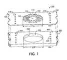
- FIG. 1is a perspective view of the upper surface of the stencil with multiple apertures in a circular pattern and the lower surface of the printed wiring board with a plated through-hole for the deposition of solder paste through the opposite surface of a printed wiring board for a component mounted on the upper surface of the printed wiring board of the present invention.
- FIG. 2is a side view of the printed wiring board with a plated through-hole for the deposition of solder paste through the opposite surface of a printed wiring board for a component mounted on the upper surface of the printed wiring board of FIG. 1.
- FIG. 3is a side view of deposition of solder paste through the stencil with multiple apertures from the opposite surface of the printed wiring board through the plated through-hole of the printed wiring board to the component mounted on the upper surface of the printed wiring board of the present invention.
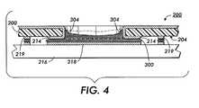
- FIG. 4is a side view of the component mounted on the upper surface of the printed wiring board of the present invention.
- FIG. 1wherein there is illustrated the stencil 100 with multiple apertures 102 for the deposition of solder paste through a through-hole to the opposite surface of a printed wiring board for mounting an electronic component in accordance with this invention.
- the stencil 100includes a thin metal sheet 104 having a plurality of apertures 102 therethrough arranged in a circular pattern corresponding to the pattern of solder paste to be deposited through a through-hole on the printed wiring board 200 .
- the thin metal sheet 104may be a sheet or membrane of brass, steel, stainless steel (magnetic or non-magnetic), carbon steel, nickel alloy, iron alloy molybdenum, titanium or other high-strength metal, their alloys, and laminates of sheets thereof.
- the plurality of apertures 102are arranged in a circular symmetrical pattern on the stencil 100 around a center point 108 and each aperture extends from the upper surface 106 of the stencil 100 through the stencil to the lower surface 110 of the stencil 100 .
- the apertures 102are identical isosceles triangular in shape with the narrow point 112 of the aperture closest to the center point 108 .
- the triangular apertureincreasing in width with radial distance from the center point.
- the widest point 114 of the aperture 102is farthest from the center point 108 .
- Each aperture in the circular patternis equidistant radially from the center point 108 and each aperture is equally spaced from the adjacent apertures.
- the circular pattern of apertures 102will have a diameter 116 at the widest point 114 of the triangular apertures 102 which is the farthest radial distance from the center point 108 of the circular pattern.
- the metal sheet 104 of stencil 100may be fabricated by at least three methods that are capable of producing apertures 102 from thin metal stencils with suitable resolution to produce fine features at fine pitch over areas as large as a printed wiring board. In general, the fabrication method producing the finest feature dimension will ordinarily also produce the lowest tolerance dimension associated with physical position over the area of the stencil.
- the lowest cost method for fabricating apertures 102 in the metal sheet 104 of stencil 100is conventional photo-etching of the sort commonly employed for fabricating thick film circuits and depositing solder paste.
- a photosensitive layeris first deposited onto a thin metal sheet, such as brass or stainless steel sheet, and is then exposed to form, for example, a cross-linked polymer.
- a pattern of openings, corresponding to the pattern of apertures 102is made in the photosensitive layer by areas which are left unexposed and are then washed away by a solvent to expose the metal sheet 104 underneath, leaving the rest of the metal sheet 104 protected by the exposed photosensitive layer.
- An acid or other etching chemicalis applied to etch away those exposed areas of metal sheet 104 to form apertures 102 therethrough in the pattern of apertures 102 .
- the current state of photo-etching technologyis able to produce a pattern of 125-micron openings in metal sheets having a thickness of 50 microns or more.
- a second method of fabricating apertures 102 in metal sheet 104 of stencil 100that is cost effective employs laser machining.
- a beam produced by a high power laser having a fine beam focusis used to heat up those areas of the metal sheet 104 at which openings, corresponding to the pattern of apertures 102 , are to be made and the energy of the laser beam vaporizes or evaporates away the metal to form apertures in the metal sheet 104 .
- the energy level of the laser beamis selected to be sufficient to vaporize the material to be removed in a controlled fashion, but is not so high as to damage surrounding areas of the material of the metal sheet 104 of stencil 100 .
- Laser machining technologycan currently machine apertures having dimensions of less than 10 microns, but at higher cost than that of photo-etching.
- the most precise aperturesmay be achieved by a third method known as electroforming.
- electroformingthe same photo-resist materials that are used in conventional semiconductor wafer processing are used to form the fine apertures 102 , and electroplating or electroforming or electro-depositing is used to build up a thin metal sheet 104 .
- Precision openings having a dimension as fine as 2.5 micronshave been fabricated by electroforming.
- the printed wiring board 200has a lower surface 202 and an upper surface 204 .
- the lower surface 202 of the printed wiring board 200is adjacent to the lower surface 110 of the stencil 100 .
- a circular through-hole 206extends from the lower surface 202 of the printed wiring board 200 through the printed wiring board to the upper surface 204 of the printed wiring board 200 .
- the through-hole 206is plated on the hole walls 208 with a metal coating 210 , preferably copper, and the coating 210 extends along the lower surface 202 of the printed wiring board 200 to form a lower pad 212 .
- the coating 210also extends along the upper surface 204 of the printed wiring board 200 to form an upper pad 214 .
- the electronic component 216 to be mounted on the lower surface 204 of the printed wiring board 200has a heat sink 218 on its lower surface.
- the heat sink 218aligns with the upper pad 214 of the printed wiring board.
- the electronic component 216is centered around the through-hole 206 .
- the electronic component 216 and the upper surface 204 of the printed wiring board 200may have additional pads 219 to be connected the printed wiring board 200 .
- the diameter 220 of the through-hole 206 of the printed wiring board 200is approximately the same as the diameter 116 of the circular pattern of the apertures 102 of the stencil 100 , specifically the widest points 114 of the apertures 102 farthest from the center point 106 of the circular pattern.
- the circular pattern of apertures 102 of the stencil 100will be aligned with the through-hole 206 of the printed wiring board 200 by alignment holes 118 on the stencil 100 and alignment holes 222 on the printed wiring board 200 .
- the stencil 100is aligned and placed in physical contact with the printed wiring board 200 at their edges by a frame (not shown) in FIG. 3.
- the lower surface 110 of the stencil 100will be in physical contact with the lower surface 202 of the printed wiring board 200 .
- the other contact pads 219 for the electronic component 216can already be bonded to the upper surface 204 of the printed wiring board 200 .
- Solder paste 300is applied to the upper surface 106 of the stencil 100 .
- a squeegee blade 302moves across the upper surface 106 forcing the solder paste 300 into the apertures 102 of the stencil 100 .
- the solder paste 300flows through the apertures 102 out the lower surface 110 of the stencil 100 , to be deposited along the walls 208 of the through-hole 206 in the printed wiring board 200 and to be deposited between the lower pad 214 on the upper surface 204 of the printed wiring board 200 and the heat sink 218 of the electronic component 216 .
- the size and shape of the aperture 102 and the movement of the squeegee blade 302controls the amount of solder paste 300 deposited between the lower pad 214 on the upper surface 204 of the printed wiring board 200 and the heat sink 218 of the electronic component 216 .
- the aperturesact as an extruding orifice through which a defined amount of solder paste is extruded between the contact pads of the printed wiring board and the electronic component.
- the length of the aperture 102 along the radial distance towards the center point 108 and the decreasing width of the aperture 102provides additional solder paste 300 along the wall 208 of the through-hole 206 and between the printed wiring board 200 and the electronic component 216 .
- the solder paste 300 along the narrower width of the aperture 102 farther away from the wall 208 of the through-hole 206will be forced through the aperture 102 by the squeegee blade 302 and droop back against the wall 208 and between the printed wiring board 200 and the electronic component 216 .
- the deposited solder paste of the present inventiondoes not take the shape of the aperture.
- a simple circular apertureinstead of the present invention, would deposit solder paste through the through-hole onto the electronic component with an excessive amount of solder paste providing an ineffective bond between the component and the printed wiring board.
- the circular symmetrical pattern of multiple identical apertures arranged at a fixed radial distance in a fixed angular configurationprovides an effective secure bond between the electronic component and the printed wiring board.
- the apertures 102need not be triangular in shape. The only shape requirement is that the apertures be identical and symmetrical around the center point to provide a uniform deposition of solder paste.
- the shape of the aperturescan be tear-drop, elliptical, rectangular or even circular.
- the diameter 116 of the circular pattern of the multiple apertures 102should match the diameter 220 of the circular through-hole 206 .
- solder paste 300melts and reflows into position.
- the solder paste 300fuses the lower pad 214 on the lower surface 204 of the printed wiring board 200 and the heat sink 218 of the electronic component 216 and forms an annular ring 304 around the circular wall of the through-hole and the electronic component.
- the screening deposition equipment suitable for use in conjunction with the present inventionincludes a mechanism for supporting the printed wiring board and the stencil and the electronic components to be mounted, for deposition of the solder paste, for driving the squeegee blade, and for heating and reflow of the solder paste in mounting the electronic component.
- the present inventionprovides an even application of solder paste to securely fasten a surface mounted electronic component to a printed wiring board.
- the solder pasteis deposited through a stencil with a circular symmetrical pattern of identical triangular apertures through a through-hole on the surface of the printed wiring board opposite the surface of the printed wiring board that the electronic components is to be mounted.
- surface mounted electronic componentsare more firmly and securely held to the printed wiring board.
- the annular solder ring 304 through the through-hole 206 to the lower surface 202 of the printed wiring board 200provides a superior thermal path for heat dissipation from the heat sink 218 of the surface mounted component 216 .
- the annular solder ring 304 through the through-hole 206 from the lower surface 202 of the printed wiring board 200 to the upper surface 204 of the printed wiring board 200also provides a low inductance electrical path to the ground layer (not shown in Figure) within a multiple layer printed wiring board 200 for the surface mounted component 216 .
Landscapes
- Engineering & Computer Science (AREA)
- Manufacturing & Machinery (AREA)
- Microelectronics & Electronic Packaging (AREA)
- Mechanical Engineering (AREA)
- Electric Connection Of Electric Components To Printed Circuits (AREA)
Abstract
Description
- The present invention relates to deposition of solder paste for surface mounted components on a printed wiring board (PWB) and, more particularly, to an aperture pattern for the deposition of solder paste through the opposite surface of a printed wiring board for surface mounted components.[0001]
- A printed wiring board is a flat plate or base of insulating material containing a pattern of conducting material. The patterned conducting material form traces which electrically connect electronic components mounted on the surface of the printed wiring board to form circuits. The surface mounted components are any of the basic electronic parts used in forming a circuit such as resistors, capacitors, DIP, integrated circuits and the like.[0002]
- The patterned conducting material in addition to forming connective traces also forms pads, conductive areas on the surface of the printing wiring board. Pads are provided on the printed wiring board so that connection can be made to the surface mounted components. The electronic components are then mounted to the appropriate pre-determined points on the conductive trace and pad pattern on the surface of the printed wiring board. Single layer printed wiring boards have all the conductors, the traces, pads and surface mounted components on one side of the board.[0003]
- In one method of mounting the electronic components on the surface of the printed wiring board, the pads can have through-holes formed from the pad through the printed wiring board. Each through-hole is coated with a conductive material along the walls of the hole. The electronic components will have connection pins which are inserted in the through-holes on the pads and then reflow soldered into position on the pads with their connective traces to the rest of the circuit.[0004]
- Alternately, electronic components can be mounted on the surface of the printed wiring board using solder paste deposited through a stencil in a desired pattern on the printed wiring board.[0005]
- The solder paste is deposited by a screen printing process using the stencil. A typical stencil will be fabricated from stainless steel foil having a thickness of the order of 0.005 or 0.006 inches (5 or 6 mils). Apertures are formed in the stencil at positions and shapes corresponding to the required component mounting pads on the printed wiring board. The stencil is precisely aligned in physical contact with the upper surface of the printed wiring board and held firmly together with the printed wiring board.[0006]
- Solder paste is applied to the upper surface of the stencil. A squeegee is then drawn through the solder paste and over the entire stencil and the solder paste is pushed into each of the apertures of the stencil and forced through the apertures onto the printed wiring board to form the solder component mounting pads on the upper surface of the printed wiring board.[0007]
- The surface mounted component itself will have contact pads or contact points. The electronic components are subsequently placed onto the printed wiring board with their contact pads mating with printed wiring board pad patterns onto which the solder paste has been precisely stenciled. The printed wiring board with electronic components thereon, then passes through an oven where the solder is melted or reflowed, thereby fusing the electronic component contact pads with the mating printed wiring board pads.[0008]
- Although use of surface mounted components generally offers high circuit densities, such components generally have significantly less mechanical strength in terms of their physical connection to the printed wiring board than components mounted by means of plated through-holes.[0009]
- An additional problem with components mounted on the surface of a printed wiring board is the heat sink for a component is typically mounted on the component between the component and the printed wiring board. This heat sink position provides a poor thermal path for dissipation of heat from the heat sink.[0010]
- A further problem for components mounted on the surface of a printed wiring board is providing a low inductance electrical path to ground within the printed wiring board.[0011]
- It is an object of this invention to provide a method and apparatus for deposition of solder paste for securely mounting electronic components on a printed wiring board.[0012]
- It is another object of this invention to provide a method and apparatus for deposition of solder paste from the opposite surface of a printed wiring board for securely mounting electronic components on a surface of the printed wiring board.[0013]
- It is yet another object of this invention to provide a thermal path for dissipation of heat from a heat sink attached to a surface mounted component from the opposite surface of a printed wiring board.[0014]
- It is yet another object of this invention to provide a low inductance electrical path to ground within the printed wiring board for the component mounted on teh surface of the printed wiring board.[0015]
- According to the present invention, a method and apparatus for depositing solder paste on a printed wiring board has a stencil with a pattern of multiple apertures. The pattern aligns with a through-hole in the printed wiring board when the stencil is in physical contact with the printed wiring board. A squeegee arrangement applies solder paste through the multiple apertures in the stencil through the through-hole of the printed wiring board to the lower surface of the printed wiring board for mounting electronic components to the lower surface of the printed wiring board.[0016]
- The circular pattern of the multiple apertures aligns with the circular through-hole. The identical triangular shape and symmetrical pattern of the apertures forces the solder paste against the wall of the through-hole.[0017]
- The resulting annular ring solder pattern in the through-hole from the opposite surface of the printed wiring board securely mounts the component to the printed wiring board, provides a low inductance electrical path to ground in the printed wiring board, and provides a superior thermal path for the heat sink of a surface mounted component.[0018]
- Other objects and attainments together with a fuller understanding of the invention will become apparent and appreciated by referring to the following description and claims taken in conjunction with the accompanying drawings.[0019]
- FIG. 1 is a perspective view of the upper surface of the stencil with multiple apertures in a circular pattern and the lower surface of the printed wiring board with a plated through-hole for the deposition of solder paste through the opposite surface of a printed wiring board for a component mounted on the upper surface of the printed wiring board of the present invention.[0020]
- FIG. 2 is a side view of the printed wiring board with a plated through-hole for the deposition of solder paste through the opposite surface of a printed wiring board for a component mounted on the upper surface of the printed wiring board of FIG. 1.[0021]
- FIG. 3 is a side view of deposition of solder paste through the stencil with multiple apertures from the opposite surface of the printed wiring board through the plated through-hole of the printed wiring board to the component mounted on the upper surface of the printed wiring board of the present invention.[0022]
- FIG. 4 is a side view of the component mounted on the upper surface of the printed wiring board of the present invention.[0023]
- Reference is now made to FIG. 1, wherein there is illustrated the[0024]
stencil 100 withmultiple apertures 102 for the deposition of solder paste through a through-hole to the opposite surface of a printed wiring board for mounting an electronic component in accordance with this invention. - In the perspective view of FIG. 1, the[0025]
stencil 100 includes athin metal sheet 104 having a plurality ofapertures 102 therethrough arranged in a circular pattern corresponding to the pattern of solder paste to be deposited through a through-hole on the printedwiring board 200. Thethin metal sheet 104 may be a sheet or membrane of brass, steel, stainless steel (magnetic or non-magnetic), carbon steel, nickel alloy, iron alloy molybdenum, titanium or other high-strength metal, their alloys, and laminates of sheets thereof. The single layerplain surface stencil 100 is fabricated from a suitable material such as rolled stainless steel foil having a thickness of typically 5 to 6 mils (1 mil=0.001 inches). The rolling process used to form such stencils produces a hard flat polishedupper surface 106 and uniform stencil thickness. - The plurality of[0026]
apertures 102 are arranged in a circular symmetrical pattern on thestencil 100 around acenter point 108 and each aperture extends from theupper surface 106 of thestencil 100 through the stencil to thelower surface 110 of thestencil 100. Theapertures 102 are identical isosceles triangular in shape with thenarrow point 112 of the aperture closest to thecenter point 108. The triangular aperture increasing in width with radial distance from the center point. Thewidest point 114 of theaperture 102 is farthest from thecenter point 108. Each aperture in the circular pattern is equidistant radially from thecenter point 108 and each aperture is equally spaced from the adjacent apertures. The circular pattern ofapertures 102 will have adiameter 116 at thewidest point 114 of thetriangular apertures 102 which is the farthest radial distance from thecenter point 108 of the circular pattern. - The[0027]
metal sheet 104 ofstencil 100 may be fabricated by at least three methods that are capable of producingapertures 102 from thin metal stencils with suitable resolution to produce fine features at fine pitch over areas as large as a printed wiring board. In general, the fabrication method producing the finest feature dimension will ordinarily also produce the lowest tolerance dimension associated with physical position over the area of the stencil. - The lowest cost method for fabricating[0028]
apertures 102 in themetal sheet 104 ofstencil 100 is conventional photo-etching of the sort commonly employed for fabricating thick film circuits and depositing solder paste. In this method, a photosensitive layer is first deposited onto a thin metal sheet, such as brass or stainless steel sheet, and is then exposed to form, for example, a cross-linked polymer. A pattern of openings, corresponding to the pattern ofapertures 102, is made in the photosensitive layer by areas which are left unexposed and are then washed away by a solvent to expose themetal sheet 104 underneath, leaving the rest of themetal sheet 104 protected by the exposed photosensitive layer. An acid or other etching chemical is applied to etch away those exposed areas ofmetal sheet 104 to formapertures 102 therethrough in the pattern ofapertures 102. The current state of photo-etching technology is able to produce a pattern of 125-micron openings in metal sheets having a thickness of 50 microns or more. - A second method of fabricating[0029]
apertures 102 inmetal sheet 104 ofstencil 100 that is cost effective employs laser machining. A beam produced by a high power laser having a fine beam focus is used to heat up those areas of themetal sheet 104 at which openings, corresponding to the pattern ofapertures 102, are to be made and the energy of the laser beam vaporizes or evaporates away the metal to form apertures in themetal sheet 104. The energy level of the laser beam is selected to be sufficient to vaporize the material to be removed in a controlled fashion, but is not so high as to damage surrounding areas of the material of themetal sheet 104 ofstencil 100. Laser machining technology can currently machine apertures having dimensions of less than 10 microns, but at higher cost than that of photo-etching. - The most precise apertures may be achieved by a third method known as electroforming. In this technique, the same photo-resist materials that are used in conventional semiconductor wafer processing are used to form the[0030]
fine apertures 102, and electroplating or electroforming or electro-depositing is used to build up athin metal sheet 104. Precision openings having a dimension as fine as 2.5 microns have been fabricated by electroforming. - Other methods, such as screen emulsion and die cutting, may also be employed. Combinations of two or three of the foregoing techniques may be employed for better cost effectiveness, such as where both fine and larger apertures are to be formed in the same metal sheet.[0031]
- As shown in the perspective view of FIG. 1 and the side view of FIG. 2, the printed[0032]
wiring board 200 has alower surface 202 and anupper surface 204. Thelower surface 202 of the printedwiring board 200 is adjacent to thelower surface 110 of thestencil 100. A circular through-hole 206 extends from thelower surface 202 of the printedwiring board 200 through the printed wiring board to theupper surface 204 of the printedwiring board 200. The through-hole 206 is plated on thehole walls 208 with ametal coating 210, preferably copper, and thecoating 210 extends along thelower surface 202 of the printedwiring board 200 to form alower pad 212. Thecoating 210 also extends along theupper surface 204 of the printedwiring board 200 to form anupper pad 214. - The[0033]
electronic component 216 to be mounted on thelower surface 204 of the printedwiring board 200 has aheat sink 218 on its lower surface. Theheat sink 218 aligns with theupper pad 214 of the printed wiring board. Theelectronic component 216 is centered around the through-hole 206. Theelectronic component 216 and theupper surface 204 of the printedwiring board 200 may haveadditional pads 219 to be connected the printedwiring board 200. - As shown in FIG. 1, the[0034]
diameter 220 of the through-hole 206 of the printedwiring board 200 is approximately the same as thediameter 116 of the circular pattern of theapertures 102 of thestencil 100, specifically thewidest points 114 of theapertures 102 farthest from thecenter point 106 of the circular pattern. The circular pattern ofapertures 102 of thestencil 100 will be aligned with the through-hole 206 of the printedwiring board 200 byalignment holes 118 on thestencil 100 andalignment holes 222 on the printedwiring board 200. - The[0035]
stencil 100 is aligned and placed in physical contact with the printedwiring board 200 at their edges by a frame (not shown) in FIG. 3. Thelower surface 110 of thestencil 100 will be in physical contact with thelower surface 202 of the printedwiring board 200. Theother contact pads 219 for theelectronic component 216 can already be bonded to theupper surface 204 of the printedwiring board 200. - [0036]
Solder paste 300 is applied to theupper surface 106 of thestencil 100. Asqueegee blade 302 moves across theupper surface 106 forcing thesolder paste 300 into theapertures 102 of thestencil 100. Thesolder paste 300 flows through theapertures 102 out thelower surface 110 of thestencil 100, to be deposited along thewalls 208 of the through-hole 206 in the printedwiring board 200 and to be deposited between thelower pad 214 on theupper surface 204 of the printedwiring board 200 and theheat sink 218 of theelectronic component 216. - The size and shape of the[0037]
aperture 102 and the movement of thesqueegee blade 302 controls the amount ofsolder paste 300 deposited between thelower pad 214 on theupper surface 204 of the printedwiring board 200 and theheat sink 218 of theelectronic component 216. In effect, the apertures act as an extruding orifice through which a defined amount of solder paste is extruded between the contact pads of the printed wiring board and the electronic component. - The triangular shape of the[0038]
aperture 102 with thewidest side 114 of thetriangular aperture 102 closest to thewall 208 of the through-hole 206 forces the depositedsolder paste 300 down thewall 208 and between the printedwiring board 200 and theelectronic component 216. - The length of the[0039]
aperture 102 along the radial distance towards thecenter point 108 and the decreasing width of theaperture 102 providesadditional solder paste 300 along thewall 208 of the through-hole 206 and between the printedwiring board 200 and theelectronic component 216. Thesolder paste 300 along the narrower width of theaperture 102 farther away from thewall 208 of the through-hole 206 will be forced through theaperture 102 by thesqueegee blade 302 and droop back against thewall 208 and between the printedwiring board 200 and theelectronic component 216. - Unlike the prior art solder deposition methods and apparatuses, the deposited solder paste of the present invention does not take the shape of the aperture. A simple circular aperture, instead of the present invention, would deposit solder paste through the through-hole onto the electronic component with an excessive amount of solder paste providing an ineffective bond between the component and the printed wiring board.[0040]
- The circular symmetrical pattern of multiple identical apertures arranged at a fixed radial distance in a fixed angular configuration provides an effective secure bond between the electronic component and the printed wiring board.[0041]
- The[0042]
apertures 102 need not be triangular in shape. The only shape requirement is that the apertures be identical and symmetrical around the center point to provide a uniform deposition of solder paste. The shape of the apertures can be tear-drop, elliptical, rectangular or even circular. Thediameter 116 of the circular pattern of themultiple apertures 102 should match thediameter 220 of the circular through-hole 206. - As shown in FIG. 4, after the[0043]
stencil 100 is removed, the printedwiring board 200 and thecomponent 216 are then heated, thesolder paste 300 melts and reflows into position. Thesolder paste 300 fuses thelower pad 214 on thelower surface 204 of the printedwiring board 200 and theheat sink 218 of theelectronic component 216 and forms anannular ring 304 around the circular wall of the through-hole and the electronic component. - The screening deposition equipment suitable for use in conjunction with the present invention includes a mechanism for supporting the printed wiring board and the stencil and the electronic components to be mounted, for deposition of the solder paste, for driving the squeegee blade, and for heating and reflow of the solder paste in mounting the electronic component.[0044]
- The present invention provides an even application of solder paste to securely fasten a surface mounted electronic component to a printed wiring board. The solder paste is deposited through a stencil with a circular symmetrical pattern of identical triangular apertures through a through-hole on the surface of the printed wiring board opposite the surface of the printed wiring board that the electronic components is to be mounted. As a result of this apparatus and method, surface mounted electronic components are more firmly and securely held to the printed wiring board.[0045]
- The[0046]
annular solder ring 304 through the through-hole 206 to thelower surface 202 of the printedwiring board 200 provides a superior thermal path for heat dissipation from theheat sink 218 of the surface mountedcomponent 216. - The[0047]
annular solder ring 304 through the through-hole 206 from thelower surface 202 of the printedwiring board 200 to theupper surface 204 of the printedwiring board 200 also provides a low inductance electrical path to the ground layer (not shown in Figure) within a multiple layer printedwiring board 200 for the surface mountedcomponent 216. - While the invention has been described in conjunction with specific embodiments, it is evident to those skilled in the art that many alternatives, modifications and variations will be apparent in light of the foregoing description. Accordingly, the invention is intended to embrace all such alternatives, modifications and variations as fall within the spirit and scope of the appended claims.[0048]
Claims (10)
Priority Applications (1)
| Application Number | Priority Date | Filing Date | Title |
|---|---|---|---|
| US10/017,598US6659328B2 (en) | 2001-12-18 | 2001-12-18 | Method and apparatus for deposition of solder paste for surface mount components on a printed wiring board |
Applications Claiming Priority (1)
| Application Number | Priority Date | Filing Date | Title |
|---|---|---|---|
| US10/017,598US6659328B2 (en) | 2001-12-18 | 2001-12-18 | Method and apparatus for deposition of solder paste for surface mount components on a printed wiring board |
Publications (2)
| Publication Number | Publication Date |
|---|---|
| US20030111518A1true US20030111518A1 (en) | 2003-06-19 |
| US6659328B2 US6659328B2 (en) | 2003-12-09 |
Family
ID=21783476
Family Applications (1)
| Application Number | Title | Priority Date | Filing Date |
|---|---|---|---|
| US10/017,598Expired - Fee RelatedUS6659328B2 (en) | 2001-12-18 | 2001-12-18 | Method and apparatus for deposition of solder paste for surface mount components on a printed wiring board |
Country Status (1)
| Country | Link |
|---|---|
| US (1) | US6659328B2 (en) |
Cited By (13)
| Publication number | Priority date | Publication date | Assignee | Title |
|---|---|---|---|---|
| WO2007077235A1 (en)* | 2005-12-30 | 2007-07-12 | Robert Bosch Gmbh | Method for producing printing masks, in particular for squeegee printing and mask |
| US20100116871A1 (en)* | 2008-11-12 | 2010-05-13 | International Business Machines Corporation | Injection molded solder method for forming solder bumps on substrates |
| US20120067412A1 (en)* | 2010-09-16 | 2012-03-22 | Weibezahn Karl S | Solder bonding entities to solid material |
| US20130025922A1 (en)* | 2011-07-29 | 2013-01-31 | Weibezahn Karl S | Bonding entities to conjoined strips of conductive material |
| US20130092721A1 (en)* | 2011-10-12 | 2013-04-18 | General Electric | Patterning method and apparatus for component boards |
| CN103085451A (en)* | 2011-11-03 | 2013-05-08 | 北大方正集团有限公司 | Silk screen printing board and preparation method thereof and printed circuit board and preparation method thereof |
| US20140367453A1 (en)* | 2011-12-21 | 2014-12-18 | Kabushiki Kaisha Nihon Micronics | Method for aligning plate-like members and method for manufacturing electrical connecting apparatus |
| US9296056B2 (en)* | 2014-07-08 | 2016-03-29 | International Business Machines Corporation | Device for thermal management of surface mount devices during reflow soldering |
| CN106624254A (en)* | 2016-12-14 | 2017-05-10 | 柳州振业焊接机电设备制造有限公司 | Automatic soldering machine |
| CN107278050A (en)* | 2017-08-07 | 2017-10-20 | 郑州云海信息技术有限公司 | A kind of asymmetric pad steel mesh windowing methods of PCBA and system |
| WO2019029920A1 (en)* | 2017-08-08 | 2019-02-14 | Continental Automotive Gmbh | METHOD FOR CONTACTING A PCB AND SUCH A PCB |
| US20190283190A1 (en)* | 2018-03-19 | 2019-09-19 | Asia Vital Components Co., Ltd. | Soldering method of soldering jig |
| CN111052882A (en)* | 2017-08-08 | 2020-04-21 | 纬湃技术有限公司 | Printing stencil for use in a method for applying a through-hole coating to a circuit board and use of the printing stencil in such a method |
Families Citing this family (6)
| Publication number | Priority date | Publication date | Assignee | Title |
|---|---|---|---|---|
| US6118080A (en)* | 1998-01-13 | 2000-09-12 | Micron Technology, Inc. | Z-axis electrical contact for microelectronic devices |
| DE10196262T1 (en)* | 2000-05-31 | 2003-05-15 | Honeywell Int Inc | filling system |
| US6843407B2 (en)* | 2001-10-12 | 2005-01-18 | Asustek Computer, Inc. | Solder bump fabrication method and apparatus |
| JP2004273438A (en)* | 2003-02-17 | 2004-09-30 | Pioneer Electronic Corp | Etching mask |
| US8916781B2 (en)* | 2011-11-15 | 2014-12-23 | Invensas Corporation | Cavities containing multi-wiring structures and devices |
| US20130133193A1 (en)* | 2011-11-28 | 2013-05-30 | Mediatek Singapore Pte. Ltd. | Surface mount technology process for advanced quad flat no-lead package process and stencil used therewith |
Family Cites Families (11)
| Publication number | Priority date | Publication date | Assignee | Title |
|---|---|---|---|---|
| US4135020A (en)* | 1975-02-24 | 1979-01-16 | Elevations/Design, Inc. | Process for producing art works and resulting product |
| US4891738A (en)* | 1988-07-26 | 1990-01-02 | Morpheus Lights, Inc. | Selectable aperture module |
| US4953460A (en)* | 1989-10-02 | 1990-09-04 | At&T Bell Laboratories | Method and apparatus for screen printing |
| US5254362A (en) | 1992-10-23 | 1993-10-19 | Motorola, Inc. | Method and apparatus for deposition of solder paste on a printed wiring board |
| DE69632537T2 (en)* | 1995-08-30 | 2005-06-02 | Matsushita Electric Industrial Co., Ltd., Kadoma | SCREEN PRINTING METHOD AND SCREEN PRINTING DEVICE |
| US5740730A (en)* | 1996-09-03 | 1998-04-21 | Micron Electronics, Inc. | Apparatus for depositing solder and adhesive materials onto a printed circuit board |
| JP3558463B2 (en)* | 1996-09-06 | 2004-08-25 | 松下電器産業株式会社 | Printing method and printing machine |
| US6276055B1 (en)* | 1998-09-02 | 2001-08-21 | Hadco Santa Clara, Inc. | Method and apparatus for forming plugs in vias of a circuit board layer |
| US6316289B1 (en) | 1998-11-12 | 2001-11-13 | Amerasia International Technology Inc. | Method of forming fine-pitch interconnections employing a standoff mask |
| TW409490B (en)* | 1998-12-31 | 2000-10-21 | World Wiser Electronics Inc | The equipment for plug hole process and the method thereof |
| US6095041A (en)* | 1999-07-22 | 2000-08-01 | International Business Corporation | Stencil mask with channels including depressions |
- 2001
- 2001-12-18USUS10/017,598patent/US6659328B2/ennot_activeExpired - Fee Related
Cited By (25)
| Publication number | Priority date | Publication date | Assignee | Title |
|---|---|---|---|---|
| WO2007077235A1 (en)* | 2005-12-30 | 2007-07-12 | Robert Bosch Gmbh | Method for producing printing masks, in particular for squeegee printing and mask |
| JP2009522762A (en)* | 2005-12-30 | 2009-06-11 | ローベルト ボツシユ ゲゼルシヤフト ミツト ベシユレンクテル ハフツング | Method and stencil apparatus for producing a printing stencil especially for gravure printing |
| US20090288566A1 (en)* | 2005-12-30 | 2009-11-26 | Robert Bosch Gmbh | Method for Producing Printing Stencils, Particularly for Screen Printing Methods, and a Stencil Device |
| US20100116871A1 (en)* | 2008-11-12 | 2010-05-13 | International Business Machines Corporation | Injection molded solder method for forming solder bumps on substrates |
| US7931187B2 (en)* | 2008-11-12 | 2011-04-26 | International Business Machines Corporation | Injection molded solder method for forming solder bumps on substrates |
| US20110127312A1 (en)* | 2008-11-12 | 2011-06-02 | International Business Machines Corporation | Injection Molded Solder Method for Forming Solder Bumps on Substrates |
| US8381962B2 (en) | 2008-11-12 | 2013-02-26 | International Business Machines Corporation | Injection molded solder method for forming solder bumps on substrates |
| US20120067412A1 (en)* | 2010-09-16 | 2012-03-22 | Weibezahn Karl S | Solder bonding entities to solid material |
| US8210424B2 (en)* | 2010-09-16 | 2012-07-03 | Hewlett-Packard Development Company, L.P. | Soldering entities to a monolithic metallic sheet |
| US20130025922A1 (en)* | 2011-07-29 | 2013-01-31 | Weibezahn Karl S | Bonding entities to conjoined strips of conductive material |
| US10028392B2 (en) | 2011-10-12 | 2018-07-17 | General Electric Company | Stencil set and system for printing solder paste for printed circuit boards |
| US20130092721A1 (en)* | 2011-10-12 | 2013-04-18 | General Electric | Patterning method and apparatus for component boards |
| US9426901B2 (en)* | 2011-10-12 | 2016-08-23 | General Electric Company | Patterning method for component boards |
| CN103085451A (en)* | 2011-11-03 | 2013-05-08 | 北大方正集团有限公司 | Silk screen printing board and preparation method thereof and printed circuit board and preparation method thereof |
| US20140367453A1 (en)* | 2011-12-21 | 2014-12-18 | Kabushiki Kaisha Nihon Micronics | Method for aligning plate-like members and method for manufacturing electrical connecting apparatus |
| US9116169B2 (en)* | 2011-12-21 | 2015-08-25 | Kabushiki Kaisha Nihon Micronics | Method for aligning plate-like members and method for manufacturing electrical connecting apparatus |
| US9296056B2 (en)* | 2014-07-08 | 2016-03-29 | International Business Machines Corporation | Device for thermal management of surface mount devices during reflow soldering |
| CN106624254A (en)* | 2016-12-14 | 2017-05-10 | 柳州振业焊接机电设备制造有限公司 | Automatic soldering machine |
| CN107278050A (en)* | 2017-08-07 | 2017-10-20 | 郑州云海信息技术有限公司 | A kind of asymmetric pad steel mesh windowing methods of PCBA and system |
| WO2019029920A1 (en)* | 2017-08-08 | 2019-02-14 | Continental Automotive Gmbh | METHOD FOR CONTACTING A PCB AND SUCH A PCB |
| CN111052882A (en)* | 2017-08-08 | 2020-04-21 | 纬湃技术有限公司 | Printing stencil for use in a method for applying a through-hole coating to a circuit board and use of the printing stencil in such a method |
| CN111052886A (en)* | 2017-08-08 | 2020-04-21 | 纬湃技术有限公司 | Method for applying a through-hole plating to a circuit board and such a circuit board |
| US10842030B2 (en)* | 2017-08-08 | 2020-11-17 | Vitesco Technologies GmbH | Method for through-plating a printed circuit board and such a printed circuit board |
| US20190283190A1 (en)* | 2018-03-19 | 2019-09-19 | Asia Vital Components Co., Ltd. | Soldering method of soldering jig |
| US10695875B2 (en)* | 2018-03-19 | 2020-06-30 | Asia Vital Components Co., Ltd. | Soldering method of soldering jig |
Also Published As
| Publication number | Publication date |
|---|---|
| US6659328B2 (en) | 2003-12-09 |
Similar Documents
| Publication | Publication Date | Title |
|---|---|---|
| US6659328B2 (en) | Method and apparatus for deposition of solder paste for surface mount components on a printed wiring board | |
| US6316289B1 (en) | Method of forming fine-pitch interconnections employing a standoff mask | |
| US4985601A (en) | Circuit boards with recessed traces | |
| KR100188625B1 (en) | Fine pitch solder deposits on printed circuit board process and product | |
| US6406988B1 (en) | Method of forming fine pitch interconnections employing magnetic masks | |
| US6902660B2 (en) | Method of manufacturing printed circuit board and multi-layered PCB | |
| WO1991014015A1 (en) | Method and materials for forming multi-layer circuits by an additive process | |
| KR19980064450A (en) | Process of forming metal stand-offs in electronic circuits | |
| CN114222445A (en) | Circuit board manufacturing method and circuit board | |
| EP1855515A1 (en) | Printed board and method for manufacturing same | |
| JP3017752B2 (en) | Printing metal mask and manufacturing method thereof | |
| KR100714774B1 (en) | Printed Circuit Board with Alloy Solder Bump and Manufacturing Method Thereof | |
| GB2247361A (en) | Conductive through-holes in printed wiring boards | |
| KR20080012310A (en) | How to Form Via Holes in Substrates for Flexible Printed Circuit Boards | |
| JPH1032371A (en) | Composite circuit board and method of manufacturing the same | |
| JPH08107263A (en) | Manufacturing method of printed wiring board | |
| JP2001196746A (en) | Printed wiring substrate and method for manufacturing printed wiring substrate | |
| JP3527965B2 (en) | Printed wiring board | |
| WO2002085081A1 (en) | Printed circuit board and production method therefor, and laminated printed circuit board | |
| JP2004064022A (en) | Printed wiring board and manufacturing method thereof | |
| US20050062587A1 (en) | Method and structure of a substrate with built-in via hole resistors | |
| KR100855808B1 (en) | Electrolytic plating equipment | |
| JPH036096A (en) | Circuit board | |
| JP3560334B2 (en) | Printed circuit board and manufacturing method thereof | |
| JPH09307201A (en) | Printed wiring board |
Legal Events
| Date | Code | Title | Description |
|---|---|---|---|
| AS | Assignment | Owner name:XEROX CORPORATION, CONNECTICUT Free format text:ASSIGNMENT OF ASSIGNORS INTEREST;ASSIGNOR:DANCES, ROBERT J.;REEL/FRAME:012385/0128 Effective date:20011212 | |
| AS | Assignment | Owner name:BANK ONE, NA, AS ADMINISTRATIVE AGENT, ILLINOIS Free format text:SECURITY AGREEMENT;ASSIGNOR:XEROX CORPORATION;REEL/FRAME:013111/0001 Effective date:20020621 Owner name:BANK ONE, NA, AS ADMINISTRATIVE AGENT,ILLINOIS Free format text:SECURITY AGREEMENT;ASSIGNOR:XEROX CORPORATION;REEL/FRAME:013111/0001 Effective date:20020621 | |
| AS | Assignment | Owner name:JPMORGAN CHASE BANK, AS COLLATERAL AGENT, TEXAS Free format text:SECURITY AGREEMENT;ASSIGNOR:XEROX CORPORATION;REEL/FRAME:015134/0476 Effective date:20030625 Owner name:JPMORGAN CHASE BANK, AS COLLATERAL AGENT,TEXAS Free format text:SECURITY AGREEMENT;ASSIGNOR:XEROX CORPORATION;REEL/FRAME:015134/0476 Effective date:20030625 | |
| AS | Assignment | Owner name:JPMORGAN CHASE BANK, AS COLLATERAL AGENT, TEXAS Free format text:SECURITY AGREEMENT;ASSIGNOR:XEROX CORPORATION;REEL/FRAME:015722/0119 Effective date:20030625 Owner name:JPMORGAN CHASE BANK, AS COLLATERAL AGENT,TEXAS Free format text:SECURITY AGREEMENT;ASSIGNOR:XEROX CORPORATION;REEL/FRAME:015722/0119 Effective date:20030625 | |
| FPAY | Fee payment | Year of fee payment:4 | |
| FPAY | Fee payment | Year of fee payment:8 | |
| REMI | Maintenance fee reminder mailed | ||
| LAPS | Lapse for failure to pay maintenance fees | ||
| STCH | Information on status: patent discontinuation | Free format text:PATENT EXPIRED DUE TO NONPAYMENT OF MAINTENANCE FEES UNDER 37 CFR 1.362 | |
| FP | Lapsed due to failure to pay maintenance fee | Effective date:20151209 | |
| AS | Assignment | Owner name:XEROX CORPORATION, CONNECTICUT Free format text:RELEASE BY SECURED PARTY;ASSIGNOR:JPMORGAN CHASE BANK, N.A. AS SUCCESSOR-IN-INTEREST ADMINISTRATIVE AGENT AND COLLATERAL AGENT TO BANK ONE, N.A.;REEL/FRAME:061360/0501 Effective date:20220822 | |
| AS | Assignment | Owner name:XEROX CORPORATION, CONNECTICUT Free format text:RELEASE BY SECURED PARTY;ASSIGNOR:JPMORGAN CHASE BANK, N.A. AS SUCCESSOR-IN-INTEREST ADMINISTRATIVE AGENT AND COLLATERAL AGENT TO BANK ONE, N.A.;REEL/FRAME:061388/0388 Effective date:20220822 Owner name:XEROX CORPORATION, CONNECTICUT Free format text:RELEASE BY SECURED PARTY;ASSIGNOR:JPMORGAN CHASE BANK, N.A. AS SUCCESSOR-IN-INTEREST ADMINISTRATIVE AGENT AND COLLATERAL AGENT TO JPMORGAN CHASE BANK;REEL/FRAME:066728/0193 Effective date:20220822 |