US20030111437A1 - Process for packaging electronic devices using thin bonding regions - Google Patents
Process for packaging electronic devices using thin bonding regionsDownload PDFInfo
- Publication number
- US20030111437A1 US20030111437A1US10/017,942US1794201AUS2003111437A1US 20030111437 A1US20030111437 A1US 20030111437A1US 1794201 AUS1794201 AUS 1794201AUS 2003111437 A1US2003111437 A1US 2003111437A1
- Authority
- US
- United States
- Prior art keywords
- cap wafer
- frit
- raised
- wafer surface
- perimeter
- Prior art date
- Legal status (The legal status is an assumption and is not a legal conclusion. Google has not performed a legal analysis and makes no representation as to the accuracy of the status listed.)
- Granted
Links
- 238000000034methodMethods0.000titleclaimsabstractdescription24
- 238000004806packaging method and processMethods0.000titleclaimsdescription5
- 239000000463materialSubstances0.000claimsabstractdescription20
- 239000011521glassSubstances0.000claimsdescription11
- 239000000758substrateSubstances0.000claimsdescription10
- 238000005530etchingMethods0.000claimsdescription6
- XLYOFNOQVPJJNP-UHFFFAOYSA-NwaterSubstancesOXLYOFNOQVPJJNP-UHFFFAOYSA-N0.000claims1
- 235000012431wafersNutrition0.000abstractdescription53
- 239000003566sealing materialSubstances0.000abstractdescription14
- 238000004519manufacturing processMethods0.000abstractdescription5
- 230000003071parasitic effectEffects0.000description4
- YCKRFDGAMUMZLT-UHFFFAOYSA-NFluorine atomChemical compound[F]YCKRFDGAMUMZLT-UHFFFAOYSA-N0.000description3
- 229910052731fluorineInorganic materials0.000description3
- 239000011737fluorineSubstances0.000description3
- XUIMIQQOPSSXEZ-UHFFFAOYSA-NSiliconChemical compound[Si]XUIMIQQOPSSXEZ-UHFFFAOYSA-N0.000description2
- 238000007789sealingMethods0.000description2
- 230000001953sensory effectEffects0.000description2
- 229910052710siliconInorganic materials0.000description2
- 239000010703siliconSubstances0.000description2
- 239000010409thin filmSubstances0.000description2
- 238000010923batch productionMethods0.000description1
- 238000000151depositionMethods0.000description1
- 230000008021depositionEffects0.000description1
- 230000000694effectsEffects0.000description1
- 230000007613environmental effectEffects0.000description1
- 238000001914filtrationMethods0.000description1
- 238000010438heat treatmentMethods0.000description1
- 230000001939inductive effectEffects0.000description1
- 238000002955isolationMethods0.000description1
- 230000000873masking effectEffects0.000description1
- 238000012986modificationMethods0.000description1
- 230000004048modificationEffects0.000description1
- 239000005022packaging materialSubstances0.000description1
- 238000005498polishingMethods0.000description1
- 239000002861polymer materialSubstances0.000description1
- 238000007650screen-printingMethods0.000description1
- 238000000926separation methodMethods0.000description1
- 239000007787solidSubstances0.000description1
- 238000000427thin-film depositionMethods0.000description1
- IGELFKKMDLGCJO-UHFFFAOYSA-Nxenon difluorideChemical compoundF[Xe]FIGELFKKMDLGCJO-UHFFFAOYSA-N0.000description1
Images


Classifications
- H—ELECTRICITY
- H03—ELECTRONIC CIRCUITRY
- H03H—IMPEDANCE NETWORKS, e.g. RESONANT CIRCUITS; RESONATORS
- H03H9/00—Networks comprising electromechanical or electro-acoustic elements; Electromechanical resonators
- H03H9/02—Details
- H03H9/05—Holders or supports
- H03H9/10—Mounting in enclosures
- H03H9/1007—Mounting in enclosures for bulk acoustic wave [BAW] devices
- H03H9/105—Mounting in enclosures for bulk acoustic wave [BAW] devices the enclosure being defined by a cover cap mounted on an element forming part of the BAW device
- H—ELECTRICITY
- H01—ELECTRIC ELEMENTS
- H01L—SEMICONDUCTOR DEVICES NOT COVERED BY CLASS H10
- H01L21/00—Processes or apparatus adapted for the manufacture or treatment of semiconductor or solid state devices or of parts thereof
- H01L21/02—Manufacture or treatment of semiconductor devices or of parts thereof
- H01L21/04—Manufacture or treatment of semiconductor devices or of parts thereof the devices having potential barriers, e.g. a PN junction, depletion layer or carrier concentration layer
- H01L21/50—Assembly of semiconductor devices using processes or apparatus not provided for in a single one of the groups H01L21/18 - H01L21/326 or H10D48/04 - H10D48/07 e.g. sealing of a cap to a base of a container
Definitions
- the present inventiongenerally relates to electronic devices and more particularly to a method for packaging devices using thin bonding regions.
- these cavitiesare formed at the wafer scale, such that a multitude of devices are made in a batch process, lowering the cost per part.
- One way to do thisis to prepare a capping wafer to be bonded to a wafer that is prepared with devices. These wafers can then be bonded together, and thereafter the devices can be singulated (e.g., separated into individual devices).
- TFRthin film resonator
- electrical signalsare transformed into acoustic waves in a piezoelectric material, the acoustic waves resonate in a prepared structure where certain frequencies are reinforced, and electrical signals are again produced by the now changed acoustic waves to produce a filtering function.
- TFRthin film resonator
- FIGS. 1 - 2 of U.S. Pat. No. 6,106,735 to Kurle et alwhere a cap wafer 3 is fabricated with webs 4 and contact holes 9 . These webs 4 are sealingly bonded to a substrate surface containing sensor components, such that gaps (caverns) are formed between adjacent webs.
- Each of these webshave bonding strips 5 (e.g., frit glass seal strips) deposited on webs 4 . These strips 5 are used for bonding the cap wafer 3 to a substrate wafer 1 .
- these frit glass seal strips 5have a line width 21 of about 500 micrometers, which corresponds to the header width of a particular web 4 .
- the frit strips shown in the prior artare typically applied with a screen printed process, and a resulting minimal linewidth is typically quite large, greater than 125 microns, as indicated in Kurle et al. This is undesirable, since these substrate surfaces (to which the cap wafer is to be attached to) contain many electrical components or sensors such as thin film resonator (TFR) components and/or filter components. From these components or devices, interconnects must be run under the frit seal in the cap wafer, and in the above example in Kurle et al., an additional 500 extra microns of “runner” are needed in order to get underneath the frit. This introduces resistive losses and additional inductive and capacitive parasitics that limit device performance. Additionally, the excessive frit width of the prior art also introduces a significant increase in die size; thus there are fewer sensory devices produced per wafer.
- TFRthin film resonator
- the present inventionprovides a method of packaging sensory devices such as RF components, where raised areas are formed on a cap wafer surface near the perimeter of a desired cavity region, such that the cap wafer surface may be bonded to a substrate surface containing RF sensor components. These raised areas can form an entire perimeter around the capping region if the cavity is desired to be sealed, and specific sealing material such as glass frit can be used, if an impervious or hermetic seal is desired.
- the cap wafer surfaceis lithographically etched at time of fabrication, so that a raised ridge is formed near the perimeter of the desired cavity region.
- the cap wafer surfaceis lithographically etched to form recesses or trenches at the cavity perimeter, each recess being filled with a sealing material, and polished if necessary to be flush with the cap wafer surface. Thereafter, the cap wafer surface (except for the filled recesses) is etched so as to form the aforementioned raised ridges.
- Etchingcan be used to remove material from a silicon capping wafer using fluorine-based chemistry XeF2 for example, which would not affect a glass-based frit material.
- the resultant cap wafer surfaceresults in a finer frit line width, much narrower than what is currently achievable.
- the raised ridge featurecan be made to any desired height and/or width so that the frit linewidth alone does not set the stand-off distance between the cap wafer surface and the substrate surface to which it is bonded.
- FIGS. 1 ( a ) and 1 ( b )illustrate bottom and side views of a capping wafer and device wafer surface in accordance with the invention
- FIG. 2illustrates an enlarged view of a raised ridge formed by the method in accordance with one embodiment of the invention
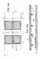
- FIGS. 3 ( a ) and 3 ( b )illustrate exemplary frit linewidth dimensions in accordance with the present invention.
- FIGS. 4 ( a )- 4 ( c )illustrate the steps of forming a raised ridge in accordance with another embodiment with the present invention.
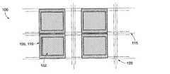
- FIGS. 1 ( a ) and 1 ( b )illustrate bottom and side views of a section of a capping wafer in accordance with the invention. It is understood that this region can be repeated to fill the area of the capping wafer 100 .
- a desired cavity region 102is defined by thin bonding strips or ridges 105 near the cavity's perimeter. As shown, the bonding strips or ridges 105 enclose the cavity region 102 entirely, but it may be desirable to only place bonding material partially around the perimeter of the cavity region 102 .
- a sealing material 110is placed on top of the bonding strips (or ridges) 105 .
- the sealing material 110bonds cap 100 to an electronic device wafer 125 upon which sits electrical connection (runner) 130 , as shown in FIG. 1( b ).
- sealing material 110is a glass frit which is screen printed on the cap wafer 100 .
- the cavity regions 102 thereby formed between cap wafer 100 and device wafer 130are then singulated, or diced as is known in the art along a cut line 115 .
- theseare cut with a diamond-tipped wet saw along saw streets 120 .
- the saw streets 120are defined by the dashed lines in FIG. 1( a ) around a cut line 115 , and similarly in the vertical direction. Saw streets 120 preferably are about 100 micrometers wide with the cut line 115 preferably about 30 micrometers wide.
- FIG. 2illustrates an enlarged view of a raised ridge formed by the method in accordance with one embodiment of the invention.
- a raised ridge 220is formed inboard from the edge of the desired cavity region 200 . Both the height and width of the ridge 220 may be adjusted to any desired dimension during initial fabrication of the cap wafer surface 202 .
- This flexibility in adjusting height and width of ridge 220encourages a different separation between the surface of a device wafer (not shown) and the cap wafer surface 202 than would be possible if the designer was strictly relying on the thickness of deposited sealing (frit) material. Also, if that height is also a critical parameter, a more reproducible standoff could be produced if the frit material is applied so as to be a small fraction of the total height, where a greater ridge definition is utilized as the majority of the total height of the ridge 220 . Further, the position of the ridge 220 on the cap wafer surface 202 can also be adjusted during fabrication of the cap wafer 200 .
- the raised ridges 220may be lithographically formed by masking the surface and then performing an etching process during time of fabrication, as is known in the art.
- the capping waferis silicon
- photo-definable resistcan be patterned in the shape of the ridges, and then fluorine-based etches can be used to remove material not masked by the resist.
- the resistcan be removed after the etch, leaving the desired ridge pattern.
- These ridges 220can then act as the bonding regions (or ridges) 105 onto which sealing material 110 is applied.
- FIGS. 3 ( a ) and 3 ( b )illustrate exemplary frit linewidth dimensions in accordance with the present invention.
- the glass frit 310is merely deposited on the flat surface 302 and has a frit linewidth of X which may be undesirably greater than 125 microns due to screen printing limitations.
- the frit linewidth of Xmay increase after frit deposition due to the lateral flow of the low-viscosity frit material.
- FIG. 3( a ) and 3 ( b )illustrate exemplary frit linewidth dimensions in accordance with the present invention.
- the glass frit 310is merely deposited on the flat surface 302 and has a frit linewidth of X which may be undesirably greater than 125 microns due to screen printing limitations.
- the frit linewidth of Xmay increase after frit deposition due to the lateral flow of the low-viscosity frit material.
- the frit linewidth dimensionis reduced to a value less than X( ⁇ X). Therefore the sealing material 310 that is printed on the raised ridge 304 is subject to a surface tension to “hold” the sealing material 310 into higher, thinner line dimensions.
- any excess materialwill flow off of the ridge 304 .
- Thisis advantageous with respect to minimizing the frit linewidth ( ⁇ X) and reducing capacitive parasitics, since not much of the surface area of the cap wafer surface 302 is in contact with the substrate surface and electrical components (not sown) attached thereto.
- shorter electrical runners(not shown in FIGS. 3 ( a ) and 3 ( b ) are needed, and therefore less of the runner is subjected to undesirable parasitics. These runners are required to go underneath the sealing material 310 to provide electrical signals to and from these components.
- FIGS. 4 ( a )- 4 ( c )illustrate process steps of forming a raised ridge 420 in a second embodiment of the present application.
- a cap wafer surface 402is trenched or etched in order to form recesses 404 .
- These recesses 404are preferably formed near the perimeter of the desired cavity region (containing the electrical devices to be capped) on cap wafer 400 , as shown in FIG. 4( a ).
- sealing material 410such as glass frit is printed into the recesses 404 , and is made flush (i.e., planarized) with the surface 402 of the cap wafer 400 , preferably by polishing if necessary.
- the fritcould be applied everywhere on the capping wafer or just spanning the recessed regions as long as material is placed into the recesses.
- the frit materialis then semi-cured to a solid state via a heating process. Thereafter in FIG.
- the areas of the cap wafer surface 402are selectively etched away (see dotted line), with the exception of the printed sealing material 410 at recesses 404 , so as to form the desired raised ridges 420 at the ends of the cap wafer surface 402 .
- surrounding wafer materialmay be etched away to a selected depth, leaving any desired standoff height, regardless of frit material height.
- a low clearance cavitycan be made if only a fraction of the recessed sealing material (glass frit) is exposed, and a deep cavity can be made by etching the cap wafer beyond the original depth of the recess by using the frit material as the etch mask, i.e. removing Si with fluorine-based chemistries that will not attack the frit.
- the method(s) of the present inventionprovide a finer frit linewidth than what than what is presently available, in order to limit the effects of capacitive parasitics, and in order to provide a device requiring smaller die such that more can be made on a wafer, and to provide a way of determining a capping cavity depth independent of frit material thickness.
Landscapes
- Physics & Mathematics (AREA)
- Engineering & Computer Science (AREA)
- Condensed Matter Physics & Semiconductors (AREA)
- General Physics & Mathematics (AREA)
- Manufacturing & Machinery (AREA)
- Computer Hardware Design (AREA)
- Microelectronics & Electronic Packaging (AREA)
- Power Engineering (AREA)
- Acoustics & Sound (AREA)
- Piezo-Electric Or Mechanical Vibrators, Or Delay Or Filter Circuits (AREA)
- Micromachines (AREA)
Abstract
Description
- 1. Field of the Invention[0001]
- The present invention generally relates to electronic devices and more particularly to a method for packaging devices using thin bonding regions.[0002]
- 2. Description of Related Art[0003]
- Electronic devices fabricated in a large scale integrated (LSI) manner by thin film deposition, etching, etc., need to be packaged so as to be easily handled, and so as to be reliable in the variety of environmental conditions that are typically present in electronic systems. In the case of most simple electronic devices, polymer materials may be applied directly on the surface of a finished device for packaging. In the case of devices that are based on acoustic waves or mechanical motion, the part of the device that contains these acoustic waves must be isolated from intimate contact with packaging material, or the acoustic wave may be corrupted. The isolation can be achieved by forming a desired sized cavity of desired depth over the devices. It is preferred to form these cavities at the wafer scale, such that a multitude of devices are made in a batch process, lowering the cost per part. One way to do this is to prepare a capping wafer to be bonded to a wafer that is prepared with devices. These wafers can then be bonded together, and thereafter the devices can be singulated (e.g., separated into individual devices).[0004]
- One such type of device is a thin film resonator (TFR). In these devices, electrical signals are transformed into acoustic waves in a piezoelectric material, the acoustic waves resonate in a prepared structure where certain frequencies are reinforced, and electrical signals are again produced by the now changed acoustic waves to produce a filtering function. For example, such a TFR is disclosed in U.S. Pat. No. 6,323,744 to Barber et al. entitled “GROUNDING OF TFR LADDER FILTERS”, the entire contents of which are hereby incorporated herein by reference.[0005]
- A conventional wafer stack is described in FIGS.[0006]1-2 of U.S. Pat. No. 6,106,735 to Kurle et al, where a cap wafer3 is fabricated with webs4 and contact holes9. These webs4 are sealingly bonded to a substrate surface containing sensor components, such that gaps (caverns) are formed between adjacent webs.
- Each of these webs have bonding strips[0007]5 (e.g., frit glass seal strips) deposited on webs4. These strips5 are used for bonding the cap wafer3 to a substrate wafer1. In particular, these frit glass seal strips5 have a line width21 of about 500 micrometers, which corresponds to the header width of a particular web4.
- The frit strips shown in the prior art are typically applied with a screen printed process, and a resulting minimal linewidth is typically quite large, greater than 125 microns, as indicated in Kurle et al. This is undesirable, since these substrate surfaces (to which the cap wafer is to be attached to) contain many electrical components or sensors such as thin film resonator (TFR) components and/or filter components. From these components or devices, interconnects must be run under the frit seal in the cap wafer, and in the above example in Kurle et al., an additional 500 extra microns of “runner” are needed in order to get underneath the frit. This introduces resistive losses and additional inductive and capacitive parasitics that limit device performance. Additionally, the excessive frit width of the prior art also introduces a significant increase in die size; thus there are fewer sensory devices produced per wafer.[0008]
- To overcome the aforementioned problems, the present invention provides a method of packaging sensory devices such as RF components, where raised areas are formed on a cap wafer surface near the perimeter of a desired cavity region, such that the cap wafer surface may be bonded to a substrate surface containing RF sensor components. These raised areas can form an entire perimeter around the capping region if the cavity is desired to be sealed, and specific sealing material such as glass frit can be used, if an impervious or hermetic seal is desired.[0009]
- In one aspect, the cap wafer surface is lithographically etched at time of fabrication, so that a raised ridge is formed near the perimeter of the desired cavity region. In another aspect, the cap wafer surface is lithographically etched to form recesses or trenches at the cavity perimeter, each recess being filled with a sealing material, and polished if necessary to be flush with the cap wafer surface. Thereafter, the cap wafer surface (except for the filled recesses) is etched so as to form the aforementioned raised ridges.[0010]
- Etching can be used to remove material from a silicon capping wafer using fluorine-based chemistry XeF2 for example, which would not affect a glass-based frit material. The resultant cap wafer surface results in a finer frit line width, much narrower than what is currently achievable. Moreover, in either aspect the raised ridge feature can be made to any desired height and/or width so that the frit linewidth alone does not set the stand-off distance between the cap wafer surface and the substrate surface to which it is bonded.[0011]
- The present invention will become more fully understood from the detailed description given hereinbelow and the accompanying drawings, wherein like elements are represented by like reference numerals, which are given by way of illustration only and thus are not limitative of the present invention and wherein:[0012]
- FIGS.[0013]1(a) and1(b) illustrate bottom and side views of a capping wafer and device wafer surface in accordance with the invention;
- FIG. 2 illustrates an enlarged view of a raised ridge formed by the method in accordance with one embodiment of the invention;[0014]
- FIGS.[0015]3(a) and3(b) illustrate exemplary frit linewidth dimensions in accordance with the present invention; and
- FIGS.[0016]4(a)-4(c) illustrate the steps of forming a raised ridge in accordance with another embodiment with the present invention.
- FIGS.[0017]1(a) and1(b) illustrate bottom and side views of a section of a capping wafer in accordance with the invention. It is understood that this region can be repeated to fill the area of the
capping wafer 100. As shown in FIG. 1(a), a desiredcavity region 102, is defined by thin bonding strips orridges 105 near the cavity's perimeter. As shown, the bonding strips orridges 105 enclose thecavity region 102 entirely, but it may be desirable to only place bonding material partially around the perimeter of thecavity region 102. - A[0018]
sealing material 110 is placed on top of the bonding strips (or ridges)105. The sealingmaterial 110bonds cap 100 to an electronic device wafer125 upon which sits electrical connection (runner)130, as shown in FIG. 1(b). Preferably sealingmaterial 110 is a glass frit which is screen printed on thecap wafer 100. Once thebonding strips 105 and sealingmaterial 110 are formed, thecavity regions 102 thereby formed betweencap wafer 100 anddevice wafer 130, are then singulated, or diced as is known in the art along acut line 115. Preferably, these are cut with a diamond-tipped wet saw alongsaw streets 120. Thesaw streets 120 are defined by the dashed lines in FIG. 1(a) around acut line 115, and similarly in the vertical direction. Sawstreets 120 preferably are about 100 micrometers wide with thecut line 115 preferably about 30 micrometers wide. - FIG. 2 illustrates an enlarged view of a raised ridge formed by the method in accordance with one embodiment of the invention. In this cross-sectional view, and specifically as shown in the enlarged view, a raised[0019]
ridge 220 is formed inboard from the edge of the desiredcavity region 200. Both the height and width of theridge 220 may be adjusted to any desired dimension during initial fabrication of thecap wafer surface 202. - This flexibility in adjusting height and width of[0020]
ridge 220 encourages a different separation between the surface of a device wafer (not shown) and thecap wafer surface 202 than would be possible if the designer was strictly relying on the thickness of deposited sealing (frit) material. Also, if that height is also a critical parameter, a more reproducible standoff could be produced if the frit material is applied so as to be a small fraction of the total height, where a greater ridge definition is utilized as the majority of the total height of theridge 220. Further, the position of theridge 220 on thecap wafer surface 202 can also be adjusted during fabrication of thecap wafer 200. - Specifically, the[0021]
raised ridges 220 may be lithographically formed by masking the surface and then performing an etching process during time of fabrication, as is known in the art. For example, if the capping wafer is silicon, photo-definable resist can be patterned in the shape of the ridges, and then fluorine-based etches can be used to remove material not masked by the resist. The resist can be removed after the etch, leaving the desired ridge pattern. Theseridges 220 can then act as the bonding regions (or ridges)105 onto which sealingmaterial 110 is applied. - FIGS.[0022]3(a) and3(b) illustrate exemplary frit linewidth dimensions in accordance with the present invention. As shown in FIG. 3(a), on a surface of a
conventional cap wafer 300, theglass frit 310 is merely deposited on theflat surface 302 and has a frit linewidth of X which may be undesirably greater than 125 microns due to screen printing limitations. Also, the frit linewidth of X may increase after frit deposition due to the lateral flow of the low-viscosity frit material. However, and as seen in FIG. 3(b), by providing acap wafer surface 302 that has been etched so as to form raisedridges 304 onto which the sealing310 is applied, the frit linewidth dimension is reduced to a value less than X(<X). Therefore the sealingmaterial 310 that is printed on the raisedridge 304 is subject to a surface tension to “hold” the sealingmaterial 310 into higher, thinner line dimensions. - Additionally, any excess material will flow off of the[0023]
ridge 304. This is advantageous with respect to minimizing the frit linewidth (<X) and reducing capacitive parasitics, since not much of the surface area of thecap wafer surface 302 is in contact with the substrate surface and electrical components (not sown) attached thereto. Thus, shorter electrical runners (not shown in FIGS.3(a) and3(b) are needed, and therefore less of the runner is subjected to undesirable parasitics. These runners are required to go underneath the sealingmaterial 310 to provide electrical signals to and from these components. - FIGS.[0024]4(a)-4(c) illustrate process steps of forming a raised
ridge 420 in a second embodiment of the present application. As shown in FIG. 4(a), initially acap wafer surface 402 is trenched or etched in order to form recesses404. Theserecesses 404 are preferably formed near the perimeter of the desired cavity region (containing the electrical devices to be capped) oncap wafer 400, as shown in FIG. 4(a). - In FIG. 4([0025]b), sealing
material 410 such as glass frit is printed into therecesses 404, and is made flush (i.e., planarized) with thesurface 402 of thecap wafer 400, preferably by polishing if necessary. The frit could be applied everywhere on the capping wafer or just spanning the recessed regions as long as material is placed into the recesses. The frit material is then semi-cured to a solid state via a heating process. Thereafter in FIG. 4(c), the areas of thecap wafer surface 402 are selectively etched away (see dotted line), with the exception of the printedsealing material 410 atrecesses 404, so as to form the desired raisedridges 420 at the ends of thecap wafer surface 402. - Using this trench fill process in accordance with the invention, after the trench is filled, surrounding wafer material may be etched away to a selected depth, leaving any desired standoff height, regardless of frit material height. For example, a low clearance cavity can be made if only a fraction of the recessed sealing material (glass frit) is exposed, and a deep cavity can be made by etching the cap wafer beyond the original depth of the recess by using the frit material as the etch mask, i.e. removing Si with fluorine-based chemistries that will not attack the frit.[0026]
- Accordingly, the method(s) of the present invention provide a finer frit linewidth than what than what is presently available, in order to limit the effects of capacitive parasitics, and in order to provide a device requiring smaller die such that more can be made on a wafer, and to provide a way of determining a capping cavity depth independent of frit material thickness.[0027]
- The invention being thus described, it will be obvious that the same may be varied in many ways. Such variations are not to be regarded as departure from the spirit and scope of the invention, and all such modifications as would be obvious to one skilled in the art are intended to be included within the scope of the following claims.[0028]
Claims (12)
Priority Applications (1)
| Application Number | Priority Date | Filing Date | Title |
|---|---|---|---|
| US10/017,942US6890445B2 (en) | 2001-12-13 | 2001-12-13 | Process for packaging electronic devices using thin bonding regions |
Applications Claiming Priority (1)
| Application Number | Priority Date | Filing Date | Title |
|---|---|---|---|
| US10/017,942US6890445B2 (en) | 2001-12-13 | 2001-12-13 | Process for packaging electronic devices using thin bonding regions |
Publications (2)
| Publication Number | Publication Date |
|---|---|
| US20030111437A1true US20030111437A1 (en) | 2003-06-19 |
| US6890445B2 US6890445B2 (en) | 2005-05-10 |
Family
ID=21785395
Family Applications (1)
| Application Number | Title | Priority Date | Filing Date |
|---|---|---|---|
| US10/017,942Expired - LifetimeUS6890445B2 (en) | 2001-12-13 | 2001-12-13 | Process for packaging electronic devices using thin bonding regions |
Country Status (1)
| Country | Link |
|---|---|
| US (1) | US6890445B2 (en) |
Cited By (3)
| Publication number | Priority date | Publication date | Assignee | Title |
|---|---|---|---|---|
| US20050000933A1 (en)* | 2003-02-17 | 2005-01-06 | Pioneer Corporation | Etching mask |
| US20070126072A1 (en)* | 2005-12-07 | 2007-06-07 | Honeywell International Inc. | Surface acoustic wave pressure sensors |
| US20140028155A1 (en)* | 2011-04-11 | 2014-01-30 | Murata Manufacturing Co., Ltd. | Electronic component and manufacturing method for the electronic component |
Citations (4)
| Publication number | Priority date | Publication date | Assignee | Title |
|---|---|---|---|---|
| US5604160A (en)* | 1996-07-29 | 1997-02-18 | Motorola, Inc. | Method for packaging semiconductor devices |
| US5891751A (en)* | 1995-06-02 | 1999-04-06 | Kulite Semiconductor Products, Inc . | Hermetically sealed transducers and methods for producing the same |
| US6062461A (en)* | 1998-06-03 | 2000-05-16 | Delphi Technologies, Inc. | Process for bonding micromachined wafers using solder |
| US20020096421A1 (en)* | 2000-11-29 | 2002-07-25 | Cohn Michael B. | MEMS device with integral packaging |
Family Cites Families (6)
| Publication number | Priority date | Publication date | Assignee | Title |
|---|---|---|---|---|
| US4622574A (en)* | 1985-07-29 | 1986-11-11 | The Perkin-Elmer Corporation | Semiconductor chip with recessed bond pads |
| US6353287B1 (en)* | 1996-12-16 | 2002-03-05 | Matsushita Electric Industrial Co., Ltd. | Gaseous discharge panel and manufacturing method therefor |
| DE19700734B4 (en)* | 1997-01-11 | 2006-06-01 | Robert Bosch Gmbh | Method for producing sensors and non-isolated wafer stacks |
| US6400440B1 (en)* | 1999-06-23 | 2002-06-04 | International Business Machines Corporation | Passive liquid crystal display having pre-tilt control structure and light absorbent material at a center |
| KR100342047B1 (en)* | 1999-07-02 | 2002-06-27 | 김순택 | Plasma display device and manufacturing method therefor |
| US6323744B1 (en)* | 2000-02-04 | 2001-11-27 | Agere Systems Guardian Corp. | Grounding of TFR ladder filters |
- 2001
- 2001-12-13USUS10/017,942patent/US6890445B2/ennot_activeExpired - Lifetime
Patent Citations (4)
| Publication number | Priority date | Publication date | Assignee | Title |
|---|---|---|---|---|
| US5891751A (en)* | 1995-06-02 | 1999-04-06 | Kulite Semiconductor Products, Inc . | Hermetically sealed transducers and methods for producing the same |
| US5604160A (en)* | 1996-07-29 | 1997-02-18 | Motorola, Inc. | Method for packaging semiconductor devices |
| US6062461A (en)* | 1998-06-03 | 2000-05-16 | Delphi Technologies, Inc. | Process for bonding micromachined wafers using solder |
| US20020096421A1 (en)* | 2000-11-29 | 2002-07-25 | Cohn Michael B. | MEMS device with integral packaging |
Cited By (5)
| Publication number | Priority date | Publication date | Assignee | Title |
|---|---|---|---|---|
| US20050000933A1 (en)* | 2003-02-17 | 2005-01-06 | Pioneer Corporation | Etching mask |
| US20070126072A1 (en)* | 2005-12-07 | 2007-06-07 | Honeywell International Inc. | Surface acoustic wave pressure sensors |
| US7651879B2 (en)* | 2005-12-07 | 2010-01-26 | Honeywell International Inc. | Surface acoustic wave pressure sensors |
| US20140028155A1 (en)* | 2011-04-11 | 2014-01-30 | Murata Manufacturing Co., Ltd. | Electronic component and manufacturing method for the electronic component |
| US9735340B2 (en)* | 2011-04-11 | 2017-08-15 | Murata Manufacturing Co., Ltd. | Method of manufacturing an electronic component |
Also Published As
| Publication number | Publication date |
|---|---|
| US6890445B2 (en) | 2005-05-10 |
Similar Documents
| Publication | Publication Date | Title |
|---|---|---|
| US20050104204A1 (en) | Wafer-level package and its manufacturing method | |
| US5731222A (en) | Externally connected thin electronic circuit having recessed bonding pads | |
| EP2697159B1 (en) | Out-of-plane spacer defined electrode | |
| US7539003B2 (en) | Capacitive micro-electro-mechanical sensors with single crystal silicon electrodes | |
| US6552404B1 (en) | Integratable transducer structure | |
| US6913941B2 (en) | SOI polysilicon trench refill perimeter oxide anchor scheme | |
| US7161283B1 (en) | Method for placing metal contacts underneath FBAR resonators | |
| US20100044808A1 (en) | method of manufacturing a mems element | |
| US9194882B2 (en) | Inertial and pressure sensors on single chip | |
| US6462392B1 (en) | Micromechanical cap structure and the respective manufacturing method | |
| US7478562B2 (en) | High temperature LC pressure transducer and methods for making the same | |
| JP2006147995A (en) | Variable capacitance element and manufacturing method thereof | |
| US10843920B2 (en) | Suspended microelectromechanical system (MEMS) devices | |
| US6225140B1 (en) | CMOS compatable surface machined pressure sensor and method of fabricating the same | |
| US11516596B2 (en) | MEMS device and manufacturing method thereof | |
| EP2776298B1 (en) | Method of forming wide trenches using a sacrificial silicon slab | |
| KR20010072390A (en) | Micromechanical sensor and corresponding production method | |
| US6794958B2 (en) | Method of fabricating a semiconductor device and an apparatus embodying the method | |
| US6890445B2 (en) | Process for packaging electronic devices using thin bonding regions | |
| JP2006351591A (en) | Micro device and packaging method thereof | |
| US11706987B2 (en) | Semiconductor device and method of forming a semiconductor device | |
| JP6813058B2 (en) | Oscillator manufacturing method | |
| US7063796B2 (en) | Micromechanical component and method for producing the same | |
| US6975010B2 (en) | MEMS structure having a blocked-sacrificial layer support/anchor and a fabrication method of the same | |
| US7531424B1 (en) | Vacuum wafer-level packaging for SOI-MEMS devices |
Legal Events
| Date | Code | Title | Description |
|---|---|---|---|
| AS | Assignment | Owner name:AGERE SYSTEMS, INC., PENNSYLVANIA Free format text:ASSIGNMENT OF ASSIGNORS INTEREST;ASSIGNORS:BARBER, BRADLEY PAUL;DUNKLEBERGER, LARUE N.;GOODELLE, JASON PAUL;AND OTHERS;REEL/FRAME:012396/0549 Effective date:20011210 | |
| STCF | Information on status: patent grant | Free format text:PATENTED CASE | |
| FPAY | Fee payment | Year of fee payment:4 | |
| FPAY | Fee payment | Year of fee payment:8 | |
| AS | Assignment | Owner name:DEUTSCHE BANK AG NEW YORK BRANCH, AS COLLATERAL AG Free format text:PATENT SECURITY AGREEMENT;ASSIGNORS:LSI CORPORATION;AGERE SYSTEMS LLC;REEL/FRAME:032856/0031 Effective date:20140506 | |
| AS | Assignment | Owner name:AGERE SYSTEMS LLC, PENNSYLVANIA Free format text:CERTIFICATE OF CONVERSION;ASSIGNOR:AGERE SYSTEMS INC.;REEL/FRAME:033663/0948 Effective date:20120730 | |
| AS | Assignment | Owner name:AVAGO TECHNOLOGIES GENERAL IP (SINGAPORE) PTE. LTD Free format text:ASSIGNMENT OF ASSIGNORS INTEREST;ASSIGNOR:AGERE SYSTEMS LLC;REEL/FRAME:035365/0634 Effective date:20140804 | |
| AS | Assignment | Owner name:LSI CORPORATION, CALIFORNIA Free format text:TERMINATION AND RELEASE OF SECURITY INTEREST IN PATENT RIGHTS (RELEASES RF 032856-0031);ASSIGNOR:DEUTSCHE BANK AG NEW YORK BRANCH, AS COLLATERAL AGENT;REEL/FRAME:037684/0039 Effective date:20160201 Owner name:AGERE SYSTEMS LLC, PENNSYLVANIA Free format text:TERMINATION AND RELEASE OF SECURITY INTEREST IN PATENT RIGHTS (RELEASES RF 032856-0031);ASSIGNOR:DEUTSCHE BANK AG NEW YORK BRANCH, AS COLLATERAL AGENT;REEL/FRAME:037684/0039 Effective date:20160201 | |
| AS | Assignment | Owner name:BANK OF AMERICA, N.A., AS COLLATERAL AGENT, NORTH CAROLINA Free format text:PATENT SECURITY AGREEMENT;ASSIGNOR:AVAGO TECHNOLOGIES GENERAL IP (SINGAPORE) PTE. LTD.;REEL/FRAME:037808/0001 Effective date:20160201 Owner name:BANK OF AMERICA, N.A., AS COLLATERAL AGENT, NORTH Free format text:PATENT SECURITY AGREEMENT;ASSIGNOR:AVAGO TECHNOLOGIES GENERAL IP (SINGAPORE) PTE. LTD.;REEL/FRAME:037808/0001 Effective date:20160201 | |
| FPAY | Fee payment | Year of fee payment:12 | |
| AS | Assignment | Owner name:AVAGO TECHNOLOGIES GENERAL IP (SINGAPORE) PTE. LTD., SINGAPORE Free format text:TERMINATION AND RELEASE OF SECURITY INTEREST IN PATENTS;ASSIGNOR:BANK OF AMERICA, N.A., AS COLLATERAL AGENT;REEL/FRAME:041710/0001 Effective date:20170119 Owner name:AVAGO TECHNOLOGIES GENERAL IP (SINGAPORE) PTE. LTD Free format text:TERMINATION AND RELEASE OF SECURITY INTEREST IN PATENTS;ASSIGNOR:BANK OF AMERICA, N.A., AS COLLATERAL AGENT;REEL/FRAME:041710/0001 Effective date:20170119 | |
| AS | Assignment | Owner name:AVAGO TECHNOLOGIES INTERNATIONAL SALES PTE. LIMITE Free format text:MERGER;ASSIGNOR:AVAGO TECHNOLOGIES GENERAL IP (SINGAPORE) PTE. LTD.;REEL/FRAME:047196/0097 Effective date:20180509 | |
| AS | Assignment | Owner name:AVAGO TECHNOLOGIES INTERNATIONAL SALES PTE. LIMITE Free format text:CORRECTIVE ASSIGNMENT TO CORRECT THE EXECUTION DATE PREVIOUSLY RECORDED AT REEL: 047196 FRAME: 0097. ASSIGNOR(S) HEREBY CONFIRMS THE MERGER;ASSIGNOR:AVAGO TECHNOLOGIES GENERAL IP (SINGAPORE) PTE. LTD.;REEL/FRAME:048555/0510 Effective date:20180905 | |
| AS | Assignment | Owner name:BROADCOM INTERNATIONAL PTE. LTD., SINGAPORE Free format text:ASSIGNMENT OF ASSIGNORS INTEREST;ASSIGNOR:AVAGO TECHNOLOGIES INTERNATIONAL SALES PTE. LIMITED;REEL/FRAME:053771/0901 Effective date:20200826 |