US20030107118A1 - Stacked packages - Google Patents
Stacked packagesDownload PDFInfo
- Publication number
- US20030107118A1 US20030107118A1US10/267,450US26745002AUS2003107118A1US 20030107118 A1US20030107118 A1US 20030107118A1US 26745002 AUS26745002 AUS 26745002AUS 2003107118 A1US2003107118 A1US 2003107118A1
- Authority
- US
- United States
- Prior art keywords
- terminals
- units
- unit
- chip
- traces
- Prior art date
- Legal status (The legal status is an assumption and is not a legal conclusion. Google has not performed a legal analysis and makes no representation as to the accuracy of the status listed.)
- Granted
Links
Images


Classifications
- H—ELECTRICITY
- H01—ELECTRIC ELEMENTS
- H01L—SEMICONDUCTOR DEVICES NOT COVERED BY CLASS H10
- H01L23/00—Details of semiconductor or other solid state devices
- H01L23/52—Arrangements for conducting electric current within the device in operation from one component to another, i.e. interconnections, e.g. wires, lead frames
- H01L23/522—Arrangements for conducting electric current within the device in operation from one component to another, i.e. interconnections, e.g. wires, lead frames including external interconnections consisting of a multilayer structure of conductive and insulating layers inseparably formed on the semiconductor body
- H01L23/528—Layout of the interconnection structure
- H—ELECTRICITY
- H01—ELECTRIC ELEMENTS
- H01L—SEMICONDUCTOR DEVICES NOT COVERED BY CLASS H10
- H01L25/00—Assemblies consisting of a plurality of semiconductor or other solid state devices
- H01L25/03—Assemblies consisting of a plurality of semiconductor or other solid state devices all the devices being of a type provided for in a single subclass of subclasses H10B, H10D, H10F, H10H, H10K or H10N, e.g. assemblies of rectifier diodes
- H01L25/04—Assemblies consisting of a plurality of semiconductor or other solid state devices all the devices being of a type provided for in a single subclass of subclasses H10B, H10D, H10F, H10H, H10K or H10N, e.g. assemblies of rectifier diodes the devices not having separate containers
- H01L25/065—Assemblies consisting of a plurality of semiconductor or other solid state devices all the devices being of a type provided for in a single subclass of subclasses H10B, H10D, H10F, H10H, H10K or H10N, e.g. assemblies of rectifier diodes the devices not having separate containers the devices being of a type provided for in group H10D89/00
- H01L25/0657—Stacked arrangements of devices
- H—ELECTRICITY
- H01—ELECTRIC ELEMENTS
- H01L—SEMICONDUCTOR DEVICES NOT COVERED BY CLASS H10
- H01L2224/00—Indexing scheme for arrangements for connecting or disconnecting semiconductor or solid-state bodies and methods related thereto as covered by H01L24/00
- H01L2224/01—Means for bonding being attached to, or being formed on, the surface to be connected, e.g. chip-to-package, die-attach, "first-level" interconnects; Manufacturing methods related thereto
- H01L2224/02—Bonding areas; Manufacturing methods related thereto
- H01L2224/04—Structure, shape, material or disposition of the bonding areas prior to the connecting process
- H01L2224/05—Structure, shape, material or disposition of the bonding areas prior to the connecting process of an individual bonding area
- H01L2224/0554—External layer
- H01L2224/05599—Material
- H—ELECTRICITY
- H01—ELECTRIC ELEMENTS
- H01L—SEMICONDUCTOR DEVICES NOT COVERED BY CLASS H10
- H01L2224/00—Indexing scheme for arrangements for connecting or disconnecting semiconductor or solid-state bodies and methods related thereto as covered by H01L24/00
- H01L2224/01—Means for bonding being attached to, or being formed on, the surface to be connected, e.g. chip-to-package, die-attach, "first-level" interconnects; Manufacturing methods related thereto
- H01L2224/42—Wire connectors; Manufacturing methods related thereto
- H01L2224/44—Structure, shape, material or disposition of the wire connectors prior to the connecting process
- H01L2224/45—Structure, shape, material or disposition of the wire connectors prior to the connecting process of an individual wire connector
- H01L2224/45001—Core members of the connector
- H01L2224/45099—Material
- H—ELECTRICITY
- H01—ELECTRIC ELEMENTS
- H01L—SEMICONDUCTOR DEVICES NOT COVERED BY CLASS H10
- H01L2224/00—Indexing scheme for arrangements for connecting or disconnecting semiconductor or solid-state bodies and methods related thereto as covered by H01L24/00
- H01L2224/01—Means for bonding being attached to, or being formed on, the surface to be connected, e.g. chip-to-package, die-attach, "first-level" interconnects; Manufacturing methods related thereto
- H01L2224/42—Wire connectors; Manufacturing methods related thereto
- H01L2224/47—Structure, shape, material or disposition of the wire connectors after the connecting process
- H01L2224/48—Structure, shape, material or disposition of the wire connectors after the connecting process of an individual wire connector
- H01L2224/481—Disposition
- H01L2224/48151—Connecting between a semiconductor or solid-state body and an item not being a semiconductor or solid-state body, e.g. chip-to-substrate, chip-to-passive
- H01L2224/48221—Connecting between a semiconductor or solid-state body and an item not being a semiconductor or solid-state body, e.g. chip-to-substrate, chip-to-passive the body and the item being stacked
- H01L2224/48225—Connecting between a semiconductor or solid-state body and an item not being a semiconductor or solid-state body, e.g. chip-to-substrate, chip-to-passive the body and the item being stacked the item being non-metallic, e.g. insulating substrate with or without metallisation
- H01L2224/4824—Connecting between the body and an opposite side of the item with respect to the body
- H—ELECTRICITY
- H01—ELECTRIC ELEMENTS
- H01L—SEMICONDUCTOR DEVICES NOT COVERED BY CLASS H10
- H01L2224/00—Indexing scheme for arrangements for connecting or disconnecting semiconductor or solid-state bodies and methods related thereto as covered by H01L24/00
- H01L2224/80—Methods for connecting semiconductor or other solid state bodies using means for bonding being attached to, or being formed on, the surface to be connected
- H01L2224/85—Methods for connecting semiconductor or other solid state bodies using means for bonding being attached to, or being formed on, the surface to be connected using a wire connector
- H01L2224/8538—Bonding interfaces outside the semiconductor or solid-state body
- H01L2224/85399—Material
- H—ELECTRICITY
- H01—ELECTRIC ELEMENTS
- H01L—SEMICONDUCTOR DEVICES NOT COVERED BY CLASS H10
- H01L2225/00—Details relating to assemblies covered by the group H01L25/00 but not provided for in its subgroups
- H01L2225/03—All the devices being of a type provided for in the same main group of the same subclass of class H10, e.g. assemblies of rectifier diodes
- H01L2225/04—All the devices being of a type provided for in the same main group of the same subclass of class H10, e.g. assemblies of rectifier diodes the devices not having separate containers
- H01L2225/065—All the devices being of a type provided for in the same main group of the same subclass of class H10
- H01L2225/06503—Stacked arrangements of devices
- H01L2225/0651—Wire or wire-like electrical connections from device to substrate
- H—ELECTRICITY
- H01—ELECTRIC ELEMENTS
- H01L—SEMICONDUCTOR DEVICES NOT COVERED BY CLASS H10
- H01L2225/00—Details relating to assemblies covered by the group H01L25/00 but not provided for in its subgroups
- H01L2225/03—All the devices being of a type provided for in the same main group of the same subclass of class H10, e.g. assemblies of rectifier diodes
- H01L2225/04—All the devices being of a type provided for in the same main group of the same subclass of class H10, e.g. assemblies of rectifier diodes the devices not having separate containers
- H01L2225/065—All the devices being of a type provided for in the same main group of the same subclass of class H10
- H01L2225/06503—Stacked arrangements of devices
- H01L2225/0652—Bump or bump-like direct electrical connections from substrate to substrate
- H—ELECTRICITY
- H01—ELECTRIC ELEMENTS
- H01L—SEMICONDUCTOR DEVICES NOT COVERED BY CLASS H10
- H01L2225/00—Details relating to assemblies covered by the group H01L25/00 but not provided for in its subgroups
- H01L2225/03—All the devices being of a type provided for in the same main group of the same subclass of class H10, e.g. assemblies of rectifier diodes
- H01L2225/04—All the devices being of a type provided for in the same main group of the same subclass of class H10, e.g. assemblies of rectifier diodes the devices not having separate containers
- H01L2225/065—All the devices being of a type provided for in the same main group of the same subclass of class H10
- H01L2225/06503—Stacked arrangements of devices
- H01L2225/06527—Special adaptation of electrical connections, e.g. rewiring, engineering changes, pressure contacts, layout
- H—ELECTRICITY
- H01—ELECTRIC ELEMENTS
- H01L—SEMICONDUCTOR DEVICES NOT COVERED BY CLASS H10
- H01L2225/00—Details relating to assemblies covered by the group H01L25/00 but not provided for in its subgroups
- H01L2225/03—All the devices being of a type provided for in the same main group of the same subclass of class H10, e.g. assemblies of rectifier diodes
- H01L2225/04—All the devices being of a type provided for in the same main group of the same subclass of class H10, e.g. assemblies of rectifier diodes the devices not having separate containers
- H01L2225/065—All the devices being of a type provided for in the same main group of the same subclass of class H10
- H01L2225/06503—Stacked arrangements of devices
- H01L2225/06541—Conductive via connections through the device, e.g. vertical interconnects, through silicon via [TSV]
- H—ELECTRICITY
- H01—ELECTRIC ELEMENTS
- H01L—SEMICONDUCTOR DEVICES NOT COVERED BY CLASS H10
- H01L2225/00—Details relating to assemblies covered by the group H01L25/00 but not provided for in its subgroups
- H01L2225/03—All the devices being of a type provided for in the same main group of the same subclass of class H10, e.g. assemblies of rectifier diodes
- H01L2225/04—All the devices being of a type provided for in the same main group of the same subclass of class H10, e.g. assemblies of rectifier diodes the devices not having separate containers
- H01L2225/065—All the devices being of a type provided for in the same main group of the same subclass of class H10
- H01L2225/06503—Stacked arrangements of devices
- H01L2225/06572—Auxiliary carrier between devices, the carrier having an electrical connection structure
- H—ELECTRICITY
- H01—ELECTRIC ELEMENTS
- H01L—SEMICONDUCTOR DEVICES NOT COVERED BY CLASS H10
- H01L2225/00—Details relating to assemblies covered by the group H01L25/00 but not provided for in its subgroups
- H01L2225/03—All the devices being of a type provided for in the same main group of the same subclass of class H10, e.g. assemblies of rectifier diodes
- H01L2225/04—All the devices being of a type provided for in the same main group of the same subclass of class H10, e.g. assemblies of rectifier diodes the devices not having separate containers
- H01L2225/065—All the devices being of a type provided for in the same main group of the same subclass of class H10
- H01L2225/06503—Stacked arrangements of devices
- H01L2225/06582—Housing for the assembly, e.g. chip scale package [CSP]
- H01L2225/06586—Housing with external bump or bump-like connectors
- H—ELECTRICITY
- H01—ELECTRIC ELEMENTS
- H01L—SEMICONDUCTOR DEVICES NOT COVERED BY CLASS H10
- H01L24/00—Arrangements for connecting or disconnecting semiconductor or solid-state bodies; Methods or apparatus related thereto
- H01L24/01—Means for bonding being attached to, or being formed on, the surface to be connected, e.g. chip-to-package, die-attach, "first-level" interconnects; Manufacturing methods related thereto
- H01L24/42—Wire connectors; Manufacturing methods related thereto
- H01L24/47—Structure, shape, material or disposition of the wire connectors after the connecting process
- H01L24/48—Structure, shape, material or disposition of the wire connectors after the connecting process of an individual wire connector
- H—ELECTRICITY
- H01—ELECTRIC ELEMENTS
- H01L—SEMICONDUCTOR DEVICES NOT COVERED BY CLASS H10
- H01L2924/00—Indexing scheme for arrangements or methods for connecting or disconnecting semiconductor or solid-state bodies as covered by H01L24/00
- H01L2924/0001—Technical content checked by a classifier
- H01L2924/00014—Technical content checked by a classifier the subject-matter covered by the group, the symbol of which is combined with the symbol of this group, being disclosed without further technical details
- H—ELECTRICITY
- H01—ELECTRIC ELEMENTS
- H01L—SEMICONDUCTOR DEVICES NOT COVERED BY CLASS H10
- H01L2924/00—Indexing scheme for arrangements or methods for connecting or disconnecting semiconductor or solid-state bodies as covered by H01L24/00
- H01L2924/01—Chemical elements
- H01L2924/01078—Platinum [Pt]
- H—ELECTRICITY
- H01—ELECTRIC ELEMENTS
- H01L—SEMICONDUCTOR DEVICES NOT COVERED BY CLASS H10
- H01L2924/00—Indexing scheme for arrangements or methods for connecting or disconnecting semiconductor or solid-state bodies as covered by H01L24/00
- H01L2924/01—Chemical elements
- H01L2924/01079—Gold [Au]
- H—ELECTRICITY
- H01—ELECTRIC ELEMENTS
- H01L—SEMICONDUCTOR DEVICES NOT COVERED BY CLASS H10
- H01L2924/00—Indexing scheme for arrangements or methods for connecting or disconnecting semiconductor or solid-state bodies as covered by H01L24/00
- H01L2924/01—Chemical elements
- H01L2924/01087—Francium [Fr]
- H—ELECTRICITY
- H01—ELECTRIC ELEMENTS
- H01L—SEMICONDUCTOR DEVICES NOT COVERED BY CLASS H10
- H01L2924/00—Indexing scheme for arrangements or methods for connecting or disconnecting semiconductor or solid-state bodies as covered by H01L24/00
- H01L2924/10—Details of semiconductor or other solid state devices to be connected
- H01L2924/11—Device type
- H01L2924/12—Passive devices, e.g. 2 terminal devices
- H01L2924/1204—Optical Diode
- H01L2924/12042—LASER
- H—ELECTRICITY
- H01—ELECTRIC ELEMENTS
- H01L—SEMICONDUCTOR DEVICES NOT COVERED BY CLASS H10
- H01L2924/00—Indexing scheme for arrangements or methods for connecting or disconnecting semiconductor or solid-state bodies as covered by H01L24/00
- H01L2924/10—Details of semiconductor or other solid state devices to be connected
- H01L2924/11—Device type
- H01L2924/14—Integrated circuits
- H01L2924/143—Digital devices
- H01L2924/1433—Application-specific integrated circuit [ASIC]
- H—ELECTRICITY
- H01—ELECTRIC ELEMENTS
- H01L—SEMICONDUCTOR DEVICES NOT COVERED BY CLASS H10
- H01L2924/00—Indexing scheme for arrangements or methods for connecting or disconnecting semiconductor or solid-state bodies as covered by H01L24/00
- H01L2924/15—Details of package parts other than the semiconductor or other solid state devices to be connected
- H01L2924/181—Encapsulation
- H—ELECTRICITY
- H01—ELECTRIC ELEMENTS
- H01L—SEMICONDUCTOR DEVICES NOT COVERED BY CLASS H10
- H01L2924/00—Indexing scheme for arrangements or methods for connecting or disconnecting semiconductor or solid-state bodies as covered by H01L24/00
- H01L2924/19—Details of hybrid assemblies other than the semiconductor or other solid state devices to be connected
- H01L2924/1901—Structure
- H01L2924/1904—Component type
- H01L2924/19041—Component type being a capacitor
- H—ELECTRICITY
- H01—ELECTRIC ELEMENTS
- H01L—SEMICONDUCTOR DEVICES NOT COVERED BY CLASS H10
- H01L2924/00—Indexing scheme for arrangements or methods for connecting or disconnecting semiconductor or solid-state bodies as covered by H01L24/00
- H01L2924/30—Technical effects
- H01L2924/301—Electrical effects
- H01L2924/30107—Inductance
- H—ELECTRICITY
- H01—ELECTRIC ELEMENTS
- H01L—SEMICONDUCTOR DEVICES NOT COVERED BY CLASS H10
- H01L2924/00—Indexing scheme for arrangements or methods for connecting or disconnecting semiconductor or solid-state bodies as covered by H01L24/00
- H01L2924/30—Technical effects
- H01L2924/301—Electrical effects
- H01L2924/3011—Impedance
- H—ELECTRICITY
- H01—ELECTRIC ELEMENTS
- H01L—SEMICONDUCTOR DEVICES NOT COVERED BY CLASS H10
- H01L2924/00—Indexing scheme for arrangements or methods for connecting or disconnecting semiconductor or solid-state bodies as covered by H01L24/00
- H01L2924/30—Technical effects
- H01L2924/301—Electrical effects
- H01L2924/3025—Electromagnetic shielding
Definitions
- Semiconductor chipstypically are thin and flat, with relatively large front and rear surfaces and small edge surfaces. The chips have contacts on their front surfaces.
- chipsare provided as packaged chips having terminals suitable for connection to an external circuit.
- Packaged chipstypically are also in the form of flat bodies. Ordinarily, the packaged chips are arranged in an array on a surface of a circuit board.
- the circuit boardhas electrical conductors, normally referred to as “traces” extending in horizontal directions parallel to the surface of the circuit board and also has contact pads or other electrically conductive elements connected to the traces.
- the packaged chipsare mounted with their terminal-bearing faces confronting the surface of the circuit board and the terminals on each packaged chip are electrically connected to the contact pads of the circuit board.
- Memory chipstypically are mounted in this manner.
- An unpackaged memory chiptypically has numerous data contacts and one or a few select contacts. The chip is arranged to ignore data or commands appearing at the data terminals unless the appropriate signals are applied to the select contact or contacts.
- a conventional packaged memory chiphas data terminals connected to the data contacts and has select terminals connected to the select contacts. In a conventional system, numerous identical packaged memory chips can be connected in an array with the corresponding data terminals of the various packaged chips connected to common traces and with the select terminals of the various chips connected to unique conductors, so that each conductor is associated with one, and only one, chip.
- Datacan be written onto an individual chip by supplying the data on the common traces and by applying a selection signal on the unique trace associated with the particular chip where the data is to be written. The remaining chips will ignore the data.
- the reverse processis employed to read data from a particular chip.
- Such a circuitcan be built readily using the conventional horizontal chip array and using identical chip packages for all of the chips in the array.
- the theoretical minimum area of the circuit boardis equal to the aggregate areas of all of the terminal-bearing surfaces of the individual chip packages.
- the circuit boardIn practice, the circuit board must be somewhat larger than this theoretical minimum.
- the traces on the circuit boardtypically have significant length and impedance so that appreciable time is required for propagation of signals along the traces. This limits the speed of operation of the circuit.
- the stacked packages shown in certain embodiments of these patentsare made by providing individual units, each including a single chip and a package element having unit terminals. Within each unit, the contacts of the chip are connected to the unit terminals. The units are stacked one atop the other. Unit terminals of each unit are connected to the corresponding unit terminals of other units. The connected unit terminals form vertical conductors of the stacked package, also referred to as buses.
- 4,956,694describes units having chip carriers with a set of intermediate terminals in each unit. These intermediate terminals are connected to the contacts on the chip and are also connected to the terminals of the unit. The interconnections are made by wire bonds. The pattern of wire bonds differs from unit to unit. This arrangement inherently requires a relatively large chip carrier, which adds to the cost and bulk of the package. Moreover, the manufacturer must handle and stock multiple different wire bonded units. Sugano et al., U.S. Pat. No. 5,198,888, uses individualized chip carriers in the various units. These chip carriers have leads defining different interconnect patterns for the select contacts and the associated terminals. This, again, adds to the cost and complexity of the manufacturing process. U.S. Pat. Nos. 6,268,649 and 6,072,233 use customized units as well. It would be desirable to reduce the cost and complexity associated with providing customized units in a stacked package.
- One aspect of the inventionprovides semiconductor chip assemblies incorporating a plurality of units.
- Each unitdesirably includes a semiconductor chip having at least one select contact and a plurality of other contacts and also includes a circuit panel having a plurality of chip select terminals and a plurality of other terminals, as well as traces extending on or in the panel.
- the tracesare electrically connected between the contacts of the chip and the terminals.
- the trace electrically connected to each chip select contact of the chipdesirably is a multi-branched trace including a common section connected to the select contact of the chip and also including a plurality of branches connected to different ones of the chip select terminals on the circuit panel.
- At least one branch, but less than all of the branches of each such multi-branch tracehave an interruption therein so that the select contact is connected to less than all of the chip select terminals on the panel and most preferably so that each chip select contact is connected to only one chip select terminal of the panel in the unit.
- the unitsare disposed one above the other in a stack of superposed units.
- the assemblyfurther includes vertical conductors, each connecting the corresponding terminals of the units in the stack to one another so as to form a plurality of vertical buses. Due to the selective connections within individual units provided by the multi-branch traces and interrupted branches, the chip select contacts of chips in different units are electrically connected to different ones of the vertical buses.
- This arrangementprovides selective routing of chip select signals and other signals which must be conveyed to individual chips.
- the remaining contacts on each chipare connected in parallel with corresponding contacts on chips in other units so that signals can be conveyed to the remaining contacts of the various chips in parallel. This provides the required selective routing.
- the chips, traces and terminals of different units in the stackare identical to one another, except that different ones of the units have different branches of their multi-branch traces interrupted so that different chip select contacts of different units are connected to different terminals on the circuit panels of such units.
- the circuit panel of each unitincludes a dielectric layer, desirably less than about 100 ⁇ m thick.
- the vertical spacing distance between corresponding features in adjacent ones of the unitsdesirably is no more than about 250 ⁇ m and preferably no more than about 200 ⁇ m greater than the thickness of the chip in each unit.
- the assemblythus, has a relatively low overall height.
- the dielectric layer in each circuit panelmay have a disconnection aperture or opening, and the interruptions in the branches of the multi-branch traces may be formed at such disconnection apertures.
- the disconnection aperturescan be formed in the dielectric layers when the units are manufactured or when the branches are interrupted, typically at a later stage in the process.
- the circuit panel of each unithas edges, and the disconnection apertures are provided in the form of notches extending inwardly from one or more of the edges.
- the terminals of such a unitmay include an outer row disposed adjacent to an edge of the circuit panel and the branches of the multi-branch traces may have portions extending outwardly to or beyond the outer row of terminals. In this instance, the notches need not extend inwardly beyond the outer row of terminals, so that the interruptions in the multi-branch leads can be formed readily.
- a further aspect of the inventionprovides methods of making a semiconductor chip assembly.
- a method according to this aspect of the inventionincludes the step of providing a plurality of units.
- each unitdesirably includes at least one semiconductor chip having at least one chip select contact and a plurality of other contacts and also includes a circuit panel having chip select terminals, other terminals and traces extending on or in the panel connected to the terminals.
- each trace of each paneldesirably is a multi-branch trace including a common section and plural branches connected to different ones of the chip select terminals
- the contacts of the at least one chip in each unitdesirably are connected to the traces of the circuit panel in that unit so that the chip select contacts are connected to the common sections of the multi-branch traces.
- the method according to this aspect of the inventiondesirably includes the step of selectively interrupting the branches of the multi-branch traces so that the common section of a multi-branch trace in each unit is connected to less than all of the chip select terminals of that unit.
- the methodpreferably includes the step of stacking the units and interconnecting terminals of different units to one another to form vertical buses.
- the selectively interrupting stepdesirably is performed so that the chip select terminals of chips in different units are connected to different ones of the vertical buses.
- the unitsare substantially identical to one another.
- the step of selectively interrupting the multi-branch tracesmay be performed at any time during or after formation of the units.
- the step of providing the unitsincludes connecting the chips to the traces using a tool such as a thermosonic bonding tool, and the step of selectively interrupting the branches is performed by engaging the same tool with the branches as part of the same processing operation.
- the step of selectively interrupting the branchesis performed later as, for example, just prior to the stacking step.
- the unitsmay be provided as substantially identical elements which may be handled and stocked as mutually interchangeable parts.
- the dielectric layers of the various unitsmay include interruption openings extending through the dielectric layers, and the branches of the multi-branch traces may extend across these interruption openings prior to the severing step.
- the step of selectively interrupting the branchesmay include breaking the branches at these interruption openings.
- the interruption openingsmay be formed at the same time as the branches are broken as, for example, by removing small regions of each multi-branch trace and portions of the dielectric layers underlying these regions, such as by punching the circuit panels to form the interruption openings while also breaking the branches of the traces.
- the unitsare substantially identical to one another and can be treated as parts interchangeable with one another up to and including the step of severing the branches, handling and stocking of the units in commerce is substantially simplified.
- the unitscan be fabricated at a chip packing plant arranged to handle bare semiconductor chips and to mount the bare semiconductor chips to the circuit panels of the individual units.
- the stacking operationcan be performed in a circuit board stuffing plant having tools and equipment adapted for surface-mounting packaged chips to circuit boards. Indeed, the stacking operation can be performed concomitantly with mounting the assembly to a circuit board.
- the unitscan be stacked and the solder balls joining the various units can be reflowed at the same time as the solder balls joining the bottom unit in the stack to the circuit board are reflowed.
- a further aspect of the inventionprovides an in-process collection of interchangeable semi-finished units usable in a stacking process and assembly as discussed above.
- a further aspect of the inventionprovides additional semiconductor chip assemblies.
- a chip assembly according to this aspect of the inventionalso includes a plurality of units, each including a semiconductor chip having contacts on a front surface, and including a circuit panel having a central region and a peripheral region.
- the paneldesirably includes a dielectric layer having first and second surfaces and at least one bond window extending between the first and second surfaces in the central region.
- the panelalso includes a plurality of terminals in the peripheral region, the terminals being exposed at both the first and second surfaces.
- the dielectric layerhas a plurality of terminal apertures extending between the first and second surfaces in the peripheral region and the terminals are pads aligned with the terminal apertures.
- the chipis disposed with the front surface of the chip facing toward a surface of the panel in the central region and the contacts of the chip are connected to the traces on the panel in the at least one bond window.
- the unitsare superposed on one another in a stack so that the rear surface of a chip in one unit faces toward a surface of the dielectric layer in a next adjacent unit.
- the unitsmost preferably bear on one another in at least those portions of the central regions occupied by the traces.
- a plurality of conductive massesare disposed between the terminals of the units and connect the terminals of the adjacent units to one another.
- the traces of each unitextend along the first surface of the dielectric layer in that unit, and the front surface of the chip in each unit faces toward the second surface of the dielectric layer in that unit.
- at least some of the unitsdesirably include heat transfer layers overlying the traces of such units, and these units bear on one another through the heat transfer layers.
- the heat transfer layer of each such unitdesirably abuts the rear surface of the chip in the next adjacent unit.
- the heat transfer layers of these unitsdesirably extend across the bond windows in the dielectric layers of these units and are substantially flat, at least in the region extending across the bond windows.
- Such unitsdesirably further include an encapsulant at least partially filling the bond windows.
- the heat transfer layersmay serve as masking layers which confine the encapsulant so that the encapsulant does not protrude beyond the dielectric layer.
- the flat heat transfer layersallow close engagement of the units with one another and good thermal contact between adjoining units.
- the heat transfer layermay be present or may be omitted, but the encapsulant defines a surface substantially flush with the first surface of the dielectric layer or recessed relative to such surface. Where the heat transfer layer is omitted, the dielectric layer of each unit may bear directly on the rear surface of the chip in the next adjoining unit.
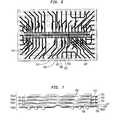
- FIG. 1is a top plan view of a circuit panel used in one embodiment of the invention.
- FIG. 2is a diagrammatic elevational view of a stacked package using the circuit panel of FIG. 1.
- FIG. 3is a diagrammatic sectional view of a stacked package in accordance with a further embodiment of the invention in conjunction with a circuit board.
- FIG. 4is a view similar to FIG. 1, but depicting a circuit panel in accordance with a further embodiment of the invention.
- FIG. 5is a view similar to FIG. 2, but depicting a stacked package using the circuit panel of FIG. 4.
- FIG. 6is a diagrammatic plan view of a circuit panel used in yet another embodiment of the invention.
- FIG. 7is a diagrammatic sectional view of a stacked package made using the circuit panel of FIG. 6.
- FIG. 8is a diagrammatic plan view of a translation panel used in a further embodiment of the invention.
- FIG. 9is a diagrammatic sectional view of a package using the translation panel of FIG. 8.
- FIG. 10is a diagrammatic sectional view of a stacked package according to a further embodiment of the invention.
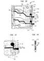
- FIG. 11is a fragmentary view of a portion of a package element in accordance with another embodiment of the invention.
- FIG. 12is a fragmentary, diagrammatic plan view of a package unit in accordance with a further embodiment of the invention.
- FIG. 13is a fragmentary plan view on an enlarged scale of the unit shown in FIG. 12.
- FIG. 14is a fragmentary, sectional elevational view taken along line 14 - 14 in FIG. 13.
- FIG. 15is a fragmentary, diagrammatic plan view of a circuit panel in accordance with yet another embodiment of the invention.
- FIG. 16is a fragmentary, diagrammatic perspective view of an in-process assemblage including a plurality of units formed using the circuit panels of FIG. 15.
- FIG. 17is a diagrammatic elevational view of a cutting tool usable with the circuit panel and units of FIGS. 15 and 16.
- FIG. 18is a fragmentary, diagrammatic plan view of a circuit panel in accordance with yet another embodiment of the invention.
- FIG. 19is a fragmentary, diagrammatic elevational view of an assembly formed from the circuit panel of FIG. 18.
- FIG. 20is a fragmentary, diagrammatic sectional view of a unit in accordance with yet another embodiment of the invention.
- a package in accordance with one embodiment of the inventionuses a plurality of package elements 20 , each such element being in the form of a circuit panel.
- Each such circuit panelmay include a dielectric layer in the form of a thin, flexible dielectric tape as, for example, a layer of reinforced or unreinforced polyimide, BT resin or the like on the order of 25-100 ⁇ m thick, most preferably 25-75 ⁇ m thick.
- each panelmay include a dielectric such as a fiberglass-reinforced epoxy as, for example, an FR-4 or FR-5 board.
- the panelhas numerous terminals 22 disposed in rows within a peripheral region of the panel, adjacent the edges 24 of the panel. In the embodiment illustrated, rows of terminals are provided along all four edges.
- each terminal 22may be in the form of a flat, relatively thin disc of copper or other suitable metallic material on a first surface 26 of the panel (the surface visible in FIG. 1). As best seen in FIG. 2, the panel also has holes 28 extending through it in alignment with terminals 22 . Each such hole extends between the first surface 26 of the panel and the opposite, second surface 30 .
- Each panel 20further has an elongated bond window 32 extending adjacent the center of the panel.
- the panelfurther has a large number of leads 36 .
- Each leadincludes a trace 38 extending along the first surface 32 of the panel and a connection section 40 formed integrally with the trace projecting from the trace across the bond window.
- each connection sectionis connected by a frangible element 42 to an anchor section 44 projecting from the side of the bond window opposite trace 38 .
- the traces and anchor portionsare arranged in a row extending along the length of the bond window. Different traces extend to opposite sides of the bond window, so that some of the connection sections 40 project into the bond window from one side, whereas others project into the bond window from the opposite side.
- the arrangement of the traces and their connection sectionsmay be substantially as shown in U.S. Pat. No. 5,489,749, the disclosure of which is hereby incorporated by reference herein.
- the terminals 22include a first set of select terminals 22 A- 22 D; a second set of select terminals 22 E- 22 H; as well as other terminals, referred to herein as non-select terminals, as, for example, terminals 22 J and 22 K.
- Each trace 38includes a common section 46 adjacent to and connected to a connection section 40 . Some of the traces are connected to the non-select terminals. These traces have common sections 46 which extend all the way to the associated terminals, such as to terminals 22 J and 22 K, so that the common section 46 of each such trace is connected directly with a non-select terminal.
- traces 38 associated with the select terminalsare multi-branched traces 50 .
- Each such multi-branched tracehas a plurality of branches connected to its common section 46 and connected to one of the associated select terminals.
- trace 38 Aincludes branch 50 A connected to select terminal 22 A; branch 50 B connected to select terminal 22 B; branch 50 C connected to select terminal 22 C; and branch 50 D connected to select terminal 22 D.
- Trace 38 Aalso includes a distribution section 52 A extending transverse to the common section 46 A and interconnecting the various branches 50 A- 50 D with the common section.
- Trace 38 E associated with terminals 22 E- 22 His also a multi-branched trace and has a similar set of branches 50 E- 50 H and distribution section 52 E, so that all of the branches 50 E- 50 H are connected to the common section 46 E of the trace and to its connection section 40 E.
- the dielectric of panel 20has disconnection apertures 54 aligned with the branches 50 of each multi-branched trace 38 , so that each such branch extends across a disconnection aperture. The disconnection apertures are disposed adjacent to the select terminals 22 A, 22 B, etc.
- the terminals and the leads, including the traces and connection sections,are formed as a single layer of metallic features on the first surface of the panel. These metallic features desirably are less than about 30 ⁇ m thick, typically about 5-25 ⁇ m thick as, for example, about 20 ⁇ m thick.
- a thin adhesive layer(not shown) optionally may be provided between the dielectric layer 20 and the metal layer. This adhesive layer should also be as thin as practicable, desirably about 15 ⁇ m or less thick.
- the terminals and tracescan be formed by conventional processes used in manufacture of tape automated bonding tapes and the like as, for example, by etching a laminate including a layer of copper or other metal and the dielectric material which forms the panel so as to remove portions of the metallic layer.
- the terminals and tracescan be formed by a deposition process such as electroless plating and/or electroplating.
- the bond window, the holes associated with the terminals and the disconnection aperturesmay be formed by etching or ablating the dielectric material.
- the stacked chip assemblyincludes a plurality of units 56 (FIG. 2). Except as otherwise stated, each unit 56 is identical to each other unit 56 in the stack. Each such unit includes a panel or chip carrier 20 as discussed above with reference to FIG. 1 and a chip 58 associated with that panel. Each such chip has a front or contact bearing surface 60 and a rear surface 62 . The front surface 60 of each chip has contacts 64 arranged in rows adjacent the center of the chip. The chip also has edges 66 bounding the front and rear surfaces 62 . The thickness t of the chip (the dimension between the front surface 60 and back surface 62 ) typically is substantially smaller than the other dimensions of the chip. For example, a typical chip may be about 100-500 microns thick and may have horizontal dimensions (in the plane of the front and rear surfaces) of about 0.5 cm or more. The front surface 60 of the chip faces towards the second surface 30 of the associated panel 20 .
- a layer of adhesive 68is disposed between the chip and the panel of each unit.
- the adhesive layer 68defines an aperture in alignment with the bond window.
- Adhesive layer 68may be provided by applying a liquid or gel material between the chip and the panel at the time of assembly or by providing a porous layer such as an array of small resilient elements between the layers and injecting a flowable material into such layer as taught, for example, in certain embodiments of U.S. Pat. Nos. 5,659,952 and 5,834,339, the disclosures of which are hereby incorporated by reference herein.
- the adhesive layeris provided as one or more solid or semi-solid pads having substantially the same horizontal extent as the desired adhesive layer in the final product.
- padsare placed between the chip and panel during assembly.
- the padmay be pre-assembled to the panel or to the chip before the chip is juxtaposed with the panel.
- Such a solid or semi-solid padcan be placed quite accurately in relation to the chip and the panel. This helps to assure that the pad does not cover terminals 22 , even where there is only a small clearance between the nominal position of the pad edge and the terminals.
- Such a padmay include an uncured or partially cured layer and other adhesion-promoting features as discussed, for example, in U.S. Pat. No. 6,030,856, the disclosure of which is hereby incorporated by reference herein.
- the padmay be provided with a thin layer of a flowable adhesive on one or both surfaces, and this layer may be a non-uniform layer as described in U.S. Pat. No. 5,548,091, the disclosure of which is hereby incorporated by reference herein, to help prevent gas entrapment in the layer during assembly.
- Adhesive layer 68desirably is as thin as practicable as, for example, about 10-125 ⁇ m thick, most preferably about 25-75 ⁇ m.
- connection section 40 of each leadis connected to a contact 64 of the chip.
- the connection section of each leadis detached from the anchor section 44 of the lead by breaking the frangible section 42 of the lead.
- This processmay be performed as described in the aforementioned U.S. Pat. No. 5,489,749 by advancing a tool (not shown) such as a thermal, thermosonic or ultrasonic bonding tool into the bond window of the panel in alignment with each connection section so that the tool captures the connection section and forces it into engagement with the appropriate contact.
- the common section 46 of the trace 38 in each leadis connected by a connection section 40 to a contact on the chip.
- the arrangement of the contacts and connection sectionsis selected so that the common sections 46 A and 46 E of multi-branched traces 38 A and 38 E are connected to select contacts on the chip, i.e., to contacts of the chip which are not to be connected in parallel with corresponding contacts on all of the other chips in the stack.
- the common sections of the other tracesare connected to the non-select contacts, i.e., contacts of the chip which are to be connected in parallel with corresponding contacts of the other chips in the stack.
- Each unit 56further includes a solder mask layer 70 (FIG. 2) overlying the traces and terminals in the peripheral region of the panel.
- the solder mask layerhas apertures aligned with the terminals 22 .
- the solder mask layercan be applied as a conformal coating or sheet by conventional processes.
- Each unitfurther includes a heat transfer layer 76 overlying the traces 38 and the first surface 26 of the panel in the central region of the panel aligned with the chip 58 . As further discussed below, the heat transfer layer will establish intimate contact with the rear surface of the chip in the next adjacent unit of the stack.
- the heat transfer layermay be formed from a material such as a gel or grease loaded with a thermally conductive filler, or from a material which can be brought to a deformable condition during assembly as, for example, a thermoplastic material or an uncured or partially cured epoxy or other reactive resin.
- the heat transfer layeris a dielectric material and hence does not electrically short the various traces to one another.
- the heat transfer layermay be formed integrally with the solder mask layer so that a central portion of the solder mask layer, aligned with chip 58 , forms the heat transfer layer.
- the heat transfer layerdesirably is as thin as practicable as, for example, about 40 ⁇ m thick or less, and desirably about 30 ⁇ m thick or less.
- An integral solder mask layer and heat transfer layermay be provided as a conformal coating having a thickness of about 5-20 ⁇ m in those regions of the coating overlying the traces and about 10-40 ⁇ m thick in those regions disposed between the traces. Such a coating adds only about 5-20 ⁇ m to the overall thickness of the unit.
- the central portion of the heat transfer layer or solder mask layerbridges across the aperture 32 in the dielectric layer.
- the central portion of the heat transfer layer or solder mask layeris substantially planar, and does not bulge substantially away from dielectric layer 20 .
- An encapsulant 33may be provided in aperture 32 , surrounding the connection sections 40 of the leads.
- the encapsulantmay be separate from the adhesive layer 68 and may be introduced using the techniques disclosed in U.S. Pat. Nos. 6,232,152 and 5,834,339, the disclosures of which are incorporated by reference herein.
- the layer attaching the chip to the dielectric layermay define a channel extending to one or both edges of the chip, and the encapsulant may be introduced into this channel at the edges of the chip.
- the encapsulantmay be formed by the flowable material.
- the heat transfer layer 76(or internal heat transfer and solder mask layer) covers the bond window in the dielectric layer so that the encapsulant cannot project beyond the first surface 76 of the dielectric layer.
- each unitDuring assembly of each unit, some of the branches of each multi-branched trace are broken so as to disconnect the terminals associated with those particular branches from the common section of the multi-branched trace. Preferably, all but one branch of each multi-branched trace is broken, leaving only one select terminal connected to the common section of each multi-branched trace.
- the branchesmay be broken by advancing a tool into the disconnection apertures 54 associated with the branches to be broken. The tool may be the same tool used to perform the bonding operation on the connection sections of the leads.
- the branchesmay be provided with frangible sections weaker than the remainder of the branch, such as narrowed sections (not shown), in alignment with the disconnection apertures.
- the terminals 22 adjacent to the branches to be brokenserve as anchors for the branches so that the branches tend to break rather than becoming detached from the dielectric of panel 20 .
- the broken ends of the branchesare not connected to any portion of the chip.
- the adhesive layer 68preferably does not include apertures aligned with the disconnection apertures and the broken ends of the branches become buried in the adhesive.
- the broken ends of the branchesmay contact the dielectric passivation layer (not shown) on the surface of the chip.
- the top unit 56 Amay have the common section 46 A of multi-branched trace 38 A connected only to terminal 22 A of set 22 A- 22 D and has the common section 46 E of trace 38 E connected only to terminal 22 E of set 22 E- 22 H.
- common section 46 Ais connected only to terminal 22 B whereas common section 46 E is connected to terminal 22 F.
- the next unit 56 Chas sections 46 A and 46 E connected to terminals 22 C and 22 G respectively, whereas the bottom unit 56 D has the same common sections connected to terminals 22 D and 22 H.
- the unitsare stacked one on top of the other as illustrated in FIG. 2.
- Each terminal 22is connected to the corresponding terminal of the next adjacent unit via a solder ball 78 .
- the solder balls 78serve as conductive elements which join the corresponding terminals of the various units into vertical conductive buses.
- terminal 22 J (FIG. 1) of each unitis connected on the same vertical bus with the corresponding terminals 22 J of the other unit.
- Each solder ballmakes contact with the terminal of one unit through an aperture in the solder mask layer 74 and with a terminal of the other unit through an aperture 28 in the dielectric layer of the panel 20 in that unit.
- the heat transfer layer 76(or the combined heat transfer and solder mask layer, where such a combined layer is employed) on each unit other than bottom unit 56 D makes intimate contact with the rear surface 62 of the chip in the next lower unit in the stack.
- the solder ballsare partially or entirely melted or “reflowed”.
- the solder mask layer 74 and the dielectric layers of the panelsprevent spreading of the solder along the lengths of the traces 38 during the reflow operation.
- the heat transfer 76 layersmay be momentarily softened during the assembly process to assure intimate contact.
- the heat transfer layersmay be cured during assembly after being brought into intimate contact with the chip of the next lower assembly.
- the individual unitsPrior to assembly of the stack, the individual units can be tested in a test socket having contacts corresponding to the locations of the terminals.
- the solder ballsare bonded to the terminals of each unit so that they project from the first surface 26 of the panel and the unit is tested with the solder balls in place.
- the test socketmay have openings adapted to engage the solder balls. Because all of the units have terminals and solder balls in the same pattern, the single test socket can be used to test all of the units.
- the resulting packagemay be assembled to a circuit board using conventional surface mounting techniques.
- the solder balls 78 of the lower most unit 56 Dcan be reflowed and bonded to contact pads 80 of a circuit board 82 , partially depicted in FIG. 2.
- each vertical busis placed in electrical contact with an individual contact pad 80 of the circuit board.
- the heat transfer layer 76 of the bottom unit 56 Dmay be in contact with a feature of circuit board 82 as, for example, a large thermal pad 84 .
- a metallic plate 86may be provided as part of the package or mounted to the circuit board prior to assembly of the package. This plate serves as a heat conductor between the thermal layer 76 and the circuit board.
- the plate or the padmay carry a layer of solder (not shown) so that the plate is reflow-bonded to the pad 84 when the solder balls are bonded to the contact pads.
- the heat transfer layer 76 of the lower-most unitmay be thick enough so that it makes direct contact with a feature of the circuit board itself.
- the heat transfer layer of the lower-most unitmay be omitted.
- the completed packageprovides numerous advantages. As discussed above, the select contacts of chips in different units are connected to different select terminals and therefore connected to different vertical buses. By routing selection signals to the contact pads of the circuit board associated with these buses, it is possible to apply a selection signal to a select contact in a chip of only one unit.
- the vertical buses formed by the interconnected solder padsare quite short and provide low electrical impedance.
- the tracesprovide a relatively lower impedance path. Typical traces have an inductance of about 5 nanohenries or less.
- signal propagation delays between the contact pads of the circuit board and the contacts of any given chipare nearly the same as the signal propagation delays between the contact pads of the circuit board and the contacts of any other chip in the package.
- the unitscan be made economically, using “single-metal”, circuit panels having conductive features on only one side.
- the entire packagehas a height which is determined in part by the thicknesses of the individual chips.
- one package which incorporates four units, each having a chip about 125 microns thick,has an overall height of about 1.5 mm.
- the low overall height of a packageis due in part to the small thickness of the elements other than the chips which determine the spacing between adjacent chips in the stack.
- the unitdesirably includes only the adhesive layer 68 , the leads or traces 38 and the heat transfer or solder mask layer and, optionally, a further adhesive layer between the dielectric layer and the metallization forming the leads.
- the distance d between corresponding features of adjacent unitsas, for example, the distance d between the second surface 30 of the dielectric layer 20 in unit 56 A and the corresponding surface of the dielectric layer in unit 56 B will be equal to the thickness t of chip 58 B disposed between these layers plus the aggregate thickness of the aforementioned layers constituting the central portion of each unit. Most preferably, the distance d between adjacent units is equal to the thickness t of the chip plus about 250 ⁇ m or less, most preferably about 200 ⁇ m or less. Still smaller distance d can be achieved when the various layers are selected to provide the minimum height.
- the heat transfer layer or combined solder mask layer and heat transfer layeris substantially flat, it can make good, intimate contact with the rear surface of the chip. This helps to provide both a low overall height and good heat transfer between units. Heat evolved in the chips of units in the middle of the stack can be dissipated by heat transfer to adjacent units through the top or bottom of the stack and from the top or bottom of the stack to the environment as, for example, to the circuit board 82 or to the surrounding atmosphere. To assure good heat transfer, and to provide the minimum overall height, it is desirable to assure that the central region of each unit is brought into abutting contact with the chip in the next adjacent unit during the stacking and reflow operations.
- the unitsalign with one another in the horizontal direction during the stacking and reflow process, using the self-centering action provided by the surface tension effects of the solder balls. If the height of the solder balls is selected to provide a nominal clearance of about 10-15 ⁇ m prior to reflowing, then upon reflowing the solder balls will initially align the units with one another and, additionally, the solder will collapse to bring the units into abutment with one another. Alternatively or additionally, the units may be pressed together during reflow to assure abutment, and may be aligned with one another using appropriate fixturing or robotic systems as, for example, systems equipped with robotic vision components.
- the unitscan be fabricated without breaking the branches 50 of the multi-branched traces. These units can be handled and stocked as interchangeable parts prior to assembly with one another and with the circuit board.
- the branchesare broken in a separate operation, desirably immediately prior to assembly.
- the step of selectively interrupting the branchesdesirably is performed in the same production plant or facility as the step of stacking the units.
- the separate branch-breaking operationdoes not require the same degree of precision required for bonding the connection sections of the leads and hence can be performed by less-precise equipment.
- units having identical chips, traces and terminals, prior to breaking the branchesare interchangeable with one another and can be provided in bulk, as a collection of interchangeable semi-finished articles.
- identicalrefers to the nominal configuration of the chips, traces and terminals, without regard for unit-to-unit variations which necessarily occur in any manufactured article.
- the stacking and branch-breaking operationsdesirably are performed in a production plant adapted for attaching packaged semiconductor chips, modules and other components to the circuit board, an operation commonly referred to in the industry as “board stuffing.”
- Board stuffing plantswhich employ surface mounting technology are commonly equipped with facilities for handling and placing components onto the circuit board, and with reflow equipment for momentarily heating the circuit board with the components thereon to fuse solder or otherwise activate bonding materials between the components and the contacts of the circuit board.
- the stacking operationcan be performed using substantially the same techniques and procedures used for mounting elements to circuit panels. Only the minimal additional operation of breaking the branches is required.
- the stacking operationcan be performed concomitantly with assembly of the stack to the board. That is, the individual units can be stacked on the circuit board, one above the other and temporarily held in place on the board as, for example, by a temporary clamping fixture, gravity, by adhesion between units, by flux at the terminals, or by some combination of these.
- the solder balls or conductive elements 78 associated with the bottom unit 56 doverly the contact pads of the circuit board and the solder balls of the other units overlies the terminals of the next lower unit in the stack.
- the entire stack and circuit panelare subjected to a reflow operation sufficient to fuse the bottom solder balls to the contact pads of the circuit board and to fuse the solder balls of the other units to the terminals of the adjacent units.
- This reflow operationmay be performed in conjunction with the reflow operation used to attach other components to the board.
- a package according to a further embodiment of the invention depicted in FIG. 3is similar to the embodiment of FIGS. 1 and 2 discussed above except that the units 156 are inverted so that the chip 158 incorporated in each unit is disposed towards the bottom of the unit whereas the circuit panel or package element 120 of each unit is disposed above the chip of that unit. Also, the solder balls 178 associated with each unit are disposed on the second or chip-facing side 130 of the panel rather than on the first or chip-remote side 126 of the panel. Stated another way, in this arrangement the solder balls are disposed on the same side of the panel as the chip. This arrangement provides lower overall height in the completed assembly.
- a thermal spreader 190is mounted to the top unit 156 A, in contact with the heat transfer layer 176 A of the top unit.
- the thermal spreader 190may be formed from a metal or other thermally conductive material and may incorporate features such as ribs or fins (not shown) for dissipating heat into the surroundings. Also, the thermal spreader may have walls extending downwardly adjacent the edges of the package toward the circuit board 182 to promote the heat transfer between the spreader and the circuit board.
- the heat transfer layer 176 provided on the first or chip-remote surface 126 of the top most unit 156 Aconforms closely to the surface of the panel 120 in such unit and to the traces 156 .
- this layermay be a dielectric layer to maintain electrical insulation between the traces of the top unit and the spreader.
- the solder mask layer 174 of the top-most unitmay extend over the traces, into the central region of the panel to provide electrical insulation for the traces.
- Similar thermal conductive layers 176are provided over the central regions of the panels in the other units.
- the solder mask layer or other dielectric layercan be used to insulate the traces if the heat transfer layer is electrically conductive. As discussed above in connection with FIGS. 1 and 2, these thermally conductive layers promote intimate contact and heat transfer between the various units in the stack. This, in turn enhances heat dissipation from the inner units of the stack.
- solder balls 178are provided on the same side of the tape as the chip, the solder balls may be surrounded wholly or partially by a stiffening layer (not shown) as disclosed in a co-pending, commonly assigned U.S. patent application Ser. No. 60/314,042, filed Aug. 22, 2001, and in the PCT international application claiming priority of same, Serial No. PCT/US02/26805, the disclosures of which are hereby incorporated by reference herein.
- a stiffening layercan be formed by a flowable material as, for example, an epoxy or encapsulant such as an epoxy or encapsulant injected between the chip and the panel of a unit to form the adhesive layer 168 .
- the stiffening layerextends towards the periphery of the panel and desirably surrounds the solder balls where the stiffening layer reinforces the panels for ease of handling during assembly. Because this layer is disposed outside of the central region, beyond the area occupied by the chips, it does not add to the height of the stack.
- the rear surface 162 of the chip in the bottom unit 156 Dfaces toward the circuit board 182 .
- Rear surface 162may be physically attached to the circuit board and placed in more intimate thermal communication with the circuit board by a thermal layer 192 provided between the rear surface of the chip and the board.
- a thermal layermay be formed from a thermally conductive material such as a gel or grease with a conductive filler or from a solder which is reflowed when the solder balls of the bottom unit are reflowed to attach the terminals to the contact pads 180 of the circuit board.
- FIGS. 4 and 5The embodiment of FIGS. 4 and 5 is similar to the embodiment discussed above with reference to FIGS. 1 and 2 except that the panel or chip carrier 320 of the lower most unit is provided with additional “dummy” terminals 323 .
- Dummy terminals 323are disposed in an array extending over the central region of the panel 320 D in the bottom unit 356 D.
- This panelalso has peripheral terminals 322 corresponding to the select terminals and non-select terminals discussed above with reference to FIG. 1.
- Solder balls 379are provided on the dummy terminals in the same manner as solder balls 378 are provided on the other terminals.
- solder ballsserve as heat conductors between the bottom unit and the circuit board when the package is mounted on a circuit board.
- the dummy terminals 323may be disconnected from the traces as shown for example at 323 B. In this arrangement, the traces 338 are routed around the dummy terminals. Alternatively or additionally as shown at 323 C, dummy terminals can be connected to the traces. This allows routing of the traces through the area occupied by the dummy terminals and hence simplifies layout of the traces on the panel.
- the panels 420 of all of the units 456 except the bottom unit 456 Dare identical to the panels discussed above with reference to FIGS. 1 and 2.
- Panel 420 D of the bottom unitis a so called “two metal” panel having a layer of metallic features 430 on the second or chip-facing side of the panel as well as separate layer of metallic features on the first or chip-remote side.
- the layer of metallic features on the chip-facing side 430includes peripheral terminals 425 and traces 439 corresponding to the terminals 422 and traces 438 of the other panels in the stack. These terminals and traces include terminals and traces essentially identical to the terminals and traces discussed above.
- the layer of metallic features on the first or chip-remote side 426 of the panelincludes an array of board connection terminals 423 disposed in a rectilinear grid extending on the central region of the panel.
- This metallic layeralso includes additional traces 433 extending from the board connection terminals 423 to vias 425 .
- the vias 425include holes extending through the panel and metallic structures such as via liners extending through these holes. Additional traces 433 are connected to traces 439 by the metallic features within the vias.
- each branch 450 of the multi-branched tracesmay be provided with a separate via 425 and linked to a separate interconnect trace 433 and board connection terminal 423 .
- FIGS. 8 and 9uses panels 520 identical to the panels discussed above with reference FIGS. 1 and 2 in all of the units 556 .
- the terminals 522 D, 556 Dare not connected directly to the circuit panel thus, the terminals of this unit are not provided with solder balls projecting downwardly.
- a further circuit panel or translator 501overlies the chip-remote or first surface of panel 520 D.
- the translatorhas board connection terminals 523 disposed in a grid like pattern similar to the pattern of board connection terminals 423 discussed above with reference to FIGS. 6 and 7.
- the translatoralso has peripheral terminals 527 in a pattern corresponding to the pattern of terminals 522 on the panels of the various units and connection traces 533 interconnecting the connection terminals 523 with the peripheral terminals 527 .
- the translatoris juxtaposed with the panel of the lower most unit so that the peripheral terminals of the translator are aligned with the peripheral terminals 522 D.
- each vertical bus defined by each set of aligned peripheral terminals on the various panels 520is electrically connected with one peripheral terminal 527 of the translator and hence with one contact pad on the circuit board. This arrangement allows fabrication of a structure with a standard or grid like terminal pattern for mounting on the circuit board with only a single metal element.
- the terminals 522 D of the bottom unitmay be solder bonded to the peripheral terminals 527 of the translator when the solder balls 578 of the next lower unit are reflowed.
- the translatormay include separate connections to separate board connection terminals 523 associated with those peripheral terminals 527 A- 527 D which will ultimately be connected to the buses associated with select terminals on the various units. This assures that each bus connected to select terminals will be connected to a unique contact pad on the circuit board.
- the translatoritself may include one or more semiconductor chips.
- the translatormay be a “bottom unit” of the type discussed in certain preferred embodiments of the co-pending, commonly assigned U.S. Provisional Patent Application Serial No. 60/408,644, entitled “Components, Methods and Assemblies For Stacked Packages,” filed on or about Sep. 6, 2002 and naming Kyong-Mo Bang as inventor, the disclosure of which is hereby incorporated by reference herein.
- a bottom unitincludes a bottom unit semiconductor chip and also includes top connections adapted to receive additional microelectronic devices.
- Such a bottom unitalso may be mounted to a circuit board in a circuit board stuffing plant and additional microelectronic devices, such as a stacked assembly as discussed herein may be mounted to the top connections of the bottom unit.
- the bottom unit chipmay be a microprocessor or other chip, whereas the chips in the stacked assembly mounted to the bottom unit may be memory chips which, in service, cooperate with the bottom unit chip.
- the package illustrated in FIG. 10is similar to the package shown in FIG. 3 except that the traces 638 of the panels 620 do not have integrally formed connection sections for bonding to the contacts 664 on the chip 658 . Instead, the traces terminate in bonding pads 637 adjacent the bond window 632 . Wire bonds 639 are provided between these bonding pads and the contacts 664 of the chip. Also, the package of FIG. 10 includes only two units rather than four units. Larger numbers and odd numbers of units also can be used in any of the foregoing structures. Wire bonded units also can be employed in the reverse orientation, i.e., with the chip of each unit disposed above the panel of the unit as discussed with reference to FIGS. 1 and 2. Also, an encapsulant 601 covers the wire bonds. The end caps may be integral with the thermally conductive layer 678 overlying the remainder of the unit.
- a multi-branched trace 639has a common section 646 which is adapted for connection to the chip contact 664 .
- the common sectionthus may have a bonding pad 637 for use with a wire bond connection to the contact or else may have a connection section which can be directly bonded to the contact.
- the branches 650 of the tracewhen initially fabricated, do not extend in an unbroken, continuous path from the common section 646 to the various select terminals 622 . Rather, each branch is initially fabricated with a gap 651 . These gaps can be selectively closed as, for example, by applying a short wire bond 653 across the gap 651 of one branch.
- the additional wire bondintroduces additional complexity and impedance and may lie above the plane of the surrounding panel.
- the gaps in the branchesare positioned in the peripheral region of the circuit panel, outside of the region occupied by the chip 658 (indicated in broken lines in FIG. 11), so that the wire bond 653 extending across the gap will lie outside of the area occupied by the chip.
- a protruding wire bond in one unit and an encapsulant which may optionally be applied over such a protruding wire bondmay project vertically beside the chip in that unit or alongside the chip in the next adjacent unit and, thus, will not add to the overall height of the stacked assembly.
- a unit in accordance with a further embodiment of the inventionincorporates a circuit panel or dielectric element 720 generally similar to the elements discussed above and having numerous terminals 722 disposed thereon and connected to numerous leads 738 .
- the terminalsinclude a first outer row 723 incorporating terminals 722 A- 722 F extending adjacent to a first edge 724 of the circuit panel. This row of terminals defines an inner border.
- Terminals 722may include additional terminals as, for example, terminals 722 G and 722 H disposed further from the edge 724 , as well as other terminals (not shown) on other parts of the circuit panel.
- the first outer row 723defines an inner border 725 at the edge of the terminals furthest from the first edge 724 of the circuit panel, a center line 726 and an outer border 731 at the edge closest to edge 724 .
- Terminals 722 C and 722 Dform a set of chip select terminals associated with a multi-branched lead 738 C having a common section 746 C adapted for connection to a chip select contact 764 and also having branches 750 C and 750 D connected to the common section.
- Branch 750 Cconnects the common section to a chip select terminal 722 C
- branch 750 Dconnects the common section 746 C to another chip select terminals 722 D.
- branches 750 C and 750 Dextend close to the first edge 724 of the circuit panel 720 .
- the branchesextend to within about 1 mm and preferably within about 0.5 mm or less of the first edge 724 , and most desirably within about 200 microns or less of the first edge.
- Branches 750 C and 750 Dare disposed outwardly of the inner border 725 of the first outer row of terminal 723 and are also disposed outwardly of the center line 727 of this row, near the outer border 731 of the row.
- the circuit panel 720has disconnection openings 754 C and 754 D in the form of notches extending inwardly from first edge 724 .
- circuit panel 720includes a structural dielectric layer 726 defining the bottom or inner surface of the circuit panel, a single layer of metallic features including the leads and terminals and, hence, including branch 750 C, and a solder mask layer 774 .
- the base dielectric layer 726 and solder mask layer 774are interrupted in the disconnection openings or notches 754 such that the branch 750 C bridges across the disconnection opening.
- Notches 754 C and 754 Dextend inwardly from edge 724 to and slightly beyond branches 750 C and 750 D. Because the branches are disposed close to the edge, the notches need not extend far into the circuit panel from the edge. Desirably, the notches extend less than about 1.5 mm and more desirably less than about 1.0 mm into the panel.
- the same structureis provided at branch 750 D and disconnection opening or notch 754 D.
- branches 750can be selectively broken by inserting a tool into the notch as, for example, a punch 702 (FIGS. 12 and 13) into the notches.
- the punchmay be moved in a direction perpendicular to the plane of the circuit panel or parallel to the plane.
- a matching die having an opening shaped to closely conform to the punchmay be provided beneath the circuit panel, and the punch may move downwardly through the notch into engagement with the die, breaking the branch lead in the process.
- branches 750 C or 750 Dcan be interrupted selectively so that the common section 746 C of lead 738 C can be connected selectively to either, both or neither of terminals 722 C and 722 D.
- An additional multi-branch lead 738 E(FIG.
- the assemblymay include additional electrical elements disposed at the top of the stack or, indeed, at any location within the stack. The additional vertical conductors formed by unconnected terminals can serve as additional conductors extending to these elements.
- the unit partially depicted in FIG. 15has a circuit panel 820 having a first edge 824 and having a first row of outer terminals 823 extending alongside of edge 824 , parallel to such edge, as well as an additional row 821 of terminals disposed inboard of the first outer row.
- a multi-branched lead 838has a common section 846 and branches 850 A, 850 B, 850 C and 850 D extending to select terminals 822 A, 822 B, 822 C and 822 D, respectively. Branches 850 are connected to the common section 846 by intermediate sections 851 .
- branches 850 A and 850 B with the common section 846connects branches 850 A and 850 B with the common section 846
- the other intermediate sectionconnects branches 850 C and 850 D with the common section.
- the branches 850extend in whole or in part outwardly beyond the center line 827 of the first outer row 823 of terminals.
- the circuit paneldoes not have disconnection openings. Instead, branches 850 are selectively severed by forming notches 854 (seen in broken lines in FIG. 15) and breaking the branches during such notch formation.
- the circuit panelmay be selectively cut by a punch to form notches 854 where the branches are to be severed, but not form notches in other locations.
- branch 850 Bwill remain unsevered and, hence, select terminal 822 B will remain connected to the common portion 846 of lead 838 , but the remaining select terminals will be disconnected.
- This operationdesirably is performed, as discussed above, prior to stacking and most desirably in the same plant where the stacking is performed as, for example, in a circuit board stuffing plant.
- a large number of unitsmay be provided as parts of a large sheet.
- one or more of the dielectric layers forming the circuit panels of the individual unitsform parts of continuous or semi-continuous dielectric layers extending throughout the sheet or tape 802 .
- the sheet or tapemay be provided with conventional registration features such as sprocket holes 804 .
- the borders of the circuit panels forming the individual unit 820are delineated in FIG. 16 for clarity of illustration, it should be appreciated that at this stage there may be no physical demarcation between adjacent units.
- the unitsare assembled in the manner discussed above by assembling semiconductor chips to the circuit panels of the individual units while leaving the units connected in the sheet 802 . At this stage, all of the units are substantially identical with one another.
- notches 854are formed in each unit in a pattern corresponding to the desired pattern of notches for that unit.
- the notches formed in different unitswill be formed in different patterns.
- a die 806has a blade portion 808 in the form of a rectangle so as to cut each unit from adjacent units and has teeth 810 adapted to cut individual notches and sever individual branches 850 (FIG. 15). Teeth 810 are arranged to sever the branches in the pattern shown in FIG. 15.
- a tooth 810 Ais provided to sever branch 850 A, and similar teeth 810 C and 810 D are provided to sever branches 850 C and 850 D.
- no toothis provided and, hence, this branch is not severed.
- the dies used to cut other units from the tapewould have a different pattern of teeth.
- Other arrangementscan be used for severing the units from the tape and concomitantly severing the branches to be used. For example, water jet, laser or other cutting devices may be used to cut individual units from the tape and also to sever the branches. Similar arrangements can be used with the other embodiments discussed above.
- the tool used to sever the unit from the sheetmay have a projection arranged to pass into such a disconnection opening and sever the branch.
- the branch-severing operationcan be performed while the various units remain connected in a sheet, desirably immediately before severing the individual units from the sheet.
- the sheetoptionally may be provided in the form of an elongated tape.
- the circuit panel 920has an edge 924 with projections 925 extending outwardly from such edge.
- a multi-branched lead 938has branches 950 extending outwardly onto the projections.
- Individual branchescan be interrupted by severing one or more of the projections as, for example, by severing projection 925 A so as to interrupt branch 950 a. This operation can be performed using a die or blade having recesses where projections are to remain attached.
- the remaining projections 925can be bent out of the plane of the circuit panel, as shown in FIG. 19 at 925 ′, so that the projections do not add substantially to the horizontal extent of the assembly.
- the various circuit panelsmay include additional features such as ground or power planes or additional layers of traces.
- the traces and other conductive features of each panelcan be placed on the second or chip-facing side of the panel rather than on the first side remote from the chip.
- the dielectric layer 1020has traces 1038 on the second or chip-facing side 1030 of dielectric layer 1020 .
- An additional solder mask layer 1002may be provided over the traces on side 1030 in addition to the solder mask layer 1076 , which also serves as the heat transfer or thermal layer of the unit.
- the encapsulant 1033 within opening 1034has a surface 1035 flush with the first surface 1026 of the dielectric layer or recessed relative to such surface, so that the first surface is substantially flat.
- the solder mask layer 1076 on the first surfacemay be removed after introduction of the encapsulant.
- the dielectric layer 1020serves as the thermal or heat transfer layer of the unit and abuts the next lower chip in the stack.
- the solder mask layer 1002 on the second or chip-facing side of the dielectric layermay be omitted or may be integrated with the adhesive layer 1068 .
- each unitcan include more than one chip.
- the chips included in the various unitsmay be memory chips as, for example, DRAM, Flash, ROM, PROM or EEPROM chips.
- the inventionalso can be employed in packaging other chips as, for example, processors or application-specific integrated circuits (ASICs).
- the “select” terminalsneed not convey a signal such as “chip select” commonly used in a memory array; any signal which is desirably routed to a specific chip or chips in a stack can be conveyed.
- the adhesive layers, leads and panelsmay be arranged to permit movement of the unit terminals of each unit with respect to the chip of that unit, so as to alleviate stresses due to thermal expansion. Also, the heat transfer layers may allow relative movement of adjacent units.
- the stacked assemblycan include one or more non-identical units in addition to the units substantially as described above.
- the different units in the stackmay include different chips.
- features discussed abovecan be used in a structure where each unit has the chip disposed in an orientation, with the rear face of the chip abutting the dielectric layer of such unit and with the contact-bearing, front face, facing away from the dielectric layer.
- the contactscan be connected to the traces by wire bonds or other conductors.
- the front face of each chip, or a layer of encapsulant overlying the front facemay abut the dielectric layer of the next adjacent unit.
- the conductive elements connecting the various units to one another and forming the vertical conductorsare conventional solder balls.
- Other conductive elementsmay be employed instead.
- so-called “solid core solder balls”can be used.
- Solid core solder ballsinclude cores formed from a material having a relatively high melting point and a solder having a melting temperature lower than the melting temperature of the core.
- Still other conductive elementscan be formed from masses of a conductive polymer composition.
Landscapes
- Engineering & Computer Science (AREA)
- Power Engineering (AREA)
- Physics & Mathematics (AREA)
- Microelectronics & Electronic Packaging (AREA)
- Condensed Matter Physics & Semiconductors (AREA)
- General Physics & Mathematics (AREA)
- Computer Hardware Design (AREA)
- Geometry (AREA)
- Structures For Mounting Electric Components On Printed Circuit Boards (AREA)
- Combinations Of Printed Boards (AREA)
Abstract
Description
- The present application claims benefit of U.S. Provisional Patent Application No. 60/328,038, filed Oct. 9, 2001, the disclosure of which is hereby incorporated by reference herein.[0001]
- Semiconductor chips typically are thin and flat, with relatively large front and rear surfaces and small edge surfaces. The chips have contacts on their front surfaces. Typically, chips are provided as packaged chips having terminals suitable for connection to an external circuit. Packaged chips typically are also in the form of flat bodies. Ordinarily, the packaged chips are arranged in an array on a surface of a circuit board. The circuit board has electrical conductors, normally referred to as “traces” extending in horizontal directions parallel to the surface of the circuit board and also has contact pads or other electrically conductive elements connected to the traces. The packaged chips are mounted with their terminal-bearing faces confronting the surface of the circuit board and the terminals on each packaged chip are electrically connected to the contact pads of the circuit board.[0002]
- Memory chips typically are mounted in this manner. An unpackaged memory chip typically has numerous data contacts and one or a few select contacts. The chip is arranged to ignore data or commands appearing at the data terminals unless the appropriate signals are applied to the select contact or contacts. A conventional packaged memory chip has data terminals connected to the data contacts and has select terminals connected to the select contacts. In a conventional system, numerous identical packaged memory chips can be connected in an array with the corresponding data terminals of the various packaged chips connected to common traces and with the select terminals of the various chips connected to unique conductors, so that each conductor is associated with one, and only one, chip. Data can be written onto an individual chip by supplying the data on the common traces and by applying a selection signal on the unique trace associated with the particular chip where the data is to be written. The remaining chips will ignore the data. The reverse process is employed to read data from a particular chip. Such a circuit can be built readily using the conventional horizontal chip array and using identical chip packages for all of the chips in the array.[0003]
- In the conventional arrangement, the theoretical minimum area of the circuit board is equal to the aggregate areas of all of the terminal-bearing surfaces of the individual chip packages. In practice, the circuit board must be somewhat larger than this theoretical minimum. The traces on the circuit board typically have significant length and impedance so that appreciable time is required for propagation of signals along the traces. This limits the speed of operation of the circuit.[0004]
- Various approaches have been proposed for alleviating these drawbacks. One such approach is to “stack” plural chips one above the other in a common package. The package itself has vertically-extending conductors that are connected to the contact pads of the circuit board. The individual chips within the package are connected to these vertically-extending conductors. Because the thickness of a chip is substantially smaller than its horizontal dimensions, the internal conductors can be shorter than the traces on a circuit board that would be required to connect the same number of chips in a conventional arrangement. Examples of stacked packages are shown, for example, in U.S. Pat. Nos. 5,861,666; 5,198,888; 4,956,694; 6,072,233; and 6,268,649. The stacked packages shown in certain embodiments of these patents are made by providing individual units, each including a single chip and a package element having unit terminals. Within each unit, the contacts of the chip are connected to the unit terminals. The units are stacked one atop the other. Unit terminals of each unit are connected to the corresponding unit terminals of other units. The connected unit terminals form vertical conductors of the stacked package, also referred to as buses.[0005]
- However, providing a circuit with individual select connections in a stacked package introduces additional complexities. Because the vertical conductors extend through the terminals of the various units, the interconnections between the contacts of the chip and the unit terminals of each unit in the stack should be different in order to provide connections to unique vertical conductors. For example, in a four-chip stack having four vertical buses for carrying selection signals, the bottom unit may have a select contact of its chip connected to a unit terminal that forms part of bus number[0006]1; the next unit may have a corresponding select contact of its chip connected to a terminal that forms bus number2; and so on. This need for customization of the units adds complexity to the manufacturing process. For example, U.S. Pat. No. 4,956,694 describes units having chip carriers with a set of intermediate terminals in each unit. These intermediate terminals are connected to the contacts on the chip and are also connected to the terminals of the unit. The interconnections are made by wire bonds. The pattern of wire bonds differs from unit to unit. This arrangement inherently requires a relatively large chip carrier, which adds to the cost and bulk of the package. Moreover, the manufacturer must handle and stock multiple different wire bonded units. Sugano et al., U.S. Pat. No. 5,198,888, uses individualized chip carriers in the various units. These chip carriers have leads defining different interconnect patterns for the select contacts and the associated terminals. This, again, adds to the cost and complexity of the manufacturing process. U.S. Pat. Nos. 6,268,649 and 6,072,233 use customized units as well. It would be desirable to reduce the cost and complexity associated with providing customized units in a stacked package.
- It would also be desirable to provide a compact stacked package and to provide a stacked package with good heat transfer from the chips within the stack to the external environment as, for example, to the circuit board or to a heat spreader overlying the top of the package. Further, it would be desirable to provide such a package using readily-available equipment and using components that can be fabricated readily.[0007]
- One aspect of the invention provides semiconductor chip assemblies incorporating a plurality of units. Each unit desirably includes a semiconductor chip having at least one select contact and a plurality of other contacts and also includes a circuit panel having a plurality of chip select terminals and a plurality of other terminals, as well as traces extending on or in the panel. The traces are electrically connected between the contacts of the chip and the terminals. The trace electrically connected to each chip select contact of the chip desirably is a multi-branched trace including a common section connected to the select contact of the chip and also including a plurality of branches connected to different ones of the chip select terminals on the circuit panel. In the assembly, desirably at least one branch, but less than all of the branches of each such multi-branch trace, have an interruption therein so that the select contact is connected to less than all of the chip select terminals on the panel and most preferably so that each chip select contact is connected to only one chip select terminal of the panel in the unit. The units are disposed one above the other in a stack of superposed units. The assembly further includes vertical conductors, each connecting the corresponding terminals of the units in the stack to one another so as to form a plurality of vertical buses. Due to the selective connections within individual units provided by the multi-branch traces and interrupted branches, the chip select contacts of chips in different units are electrically connected to different ones of the vertical buses. This arrangement provides selective routing of chip select signals and other signals which must be conveyed to individual chips. The remaining contacts on each chip are connected in parallel with corresponding contacts on chips in other units so that signals can be conveyed to the remaining contacts of the various chips in parallel. This provides the required selective routing.[0008]
- Most preferably, the chips, traces and terminals of different units in the stack are identical to one another, except that different ones of the units have different branches of their multi-branch traces interrupted so that different chip select contacts of different units are connected to different terminals on the circuit panels of such units. Most preferably, the circuit panel of each unit includes a dielectric layer, desirably less than about 100 μm thick. The vertical spacing distance between corresponding features in adjacent ones of the units desirably is no more than about 250 μm and preferably no more than about 200 μm greater than the thickness of the chip in each unit. The assembly, thus, has a relatively low overall height.[0009]
- The dielectric layer in each circuit panel may have a disconnection aperture or opening, and the interruptions in the branches of the multi-branch traces may be formed at such disconnection apertures. The disconnection apertures can be formed in the dielectric layers when the units are manufactured or when the branches are interrupted, typically at a later stage in the process. In one arrangement, the circuit panel of each unit has edges, and the disconnection apertures are provided in the form of notches extending inwardly from one or more of the edges. The terminals of such a unit may include an outer row disposed adjacent to an edge of the circuit panel and the branches of the multi-branch traces may have portions extending outwardly to or beyond the outer row of terminals. In this instance, the notches need not extend inwardly beyond the outer row of terminals, so that the interruptions in the multi-branch leads can be formed readily.[0010]
- A further aspect of the invention provides methods of making a semiconductor chip assembly. A method according to this aspect of the invention includes the step of providing a plurality of units. Here again, each unit desirably includes at least one semiconductor chip having at least one chip select contact and a plurality of other contacts and also includes a circuit panel having chip select terminals, other terminals and traces extending on or in the panel connected to the terminals. As discussed above, at least one trace of each panel desirably is a multi-branch trace including a common section and plural branches connected to different ones of the chip select terminals, and the contacts of the at least one chip in each unit desirably are connected to the traces of the circuit panel in that unit so that the chip select contacts are connected to the common sections of the multi-branch traces. The method according to this aspect of the invention desirably includes the step of selectively interrupting the branches of the multi-branch traces so that the common section of a multi-branch trace in each unit is connected to less than all of the chip select terminals of that unit. The method preferably includes the step of stacking the units and interconnecting terminals of different units to one another to form vertical buses.[0011]
- The selectively interrupting step desirably is performed so that the chip select terminals of chips in different units are connected to different ones of the vertical buses. Most preferably, prior to the step of selectively interrupting the multi-branch traces, the units are substantially identical to one another. The step of selectively interrupting the multi-branch traces may be performed at any time during or after formation of the units. In one arrangement, the step of providing the units includes connecting the chips to the traces using a tool such as a thermosonic bonding tool, and the step of selectively interrupting the branches is performed by engaging the same tool with the branches as part of the same processing operation.[0012]
- In another arrangement, the step of selectively interrupting the branches is performed later as, for example, just prior to the stacking step. Thus, the units may be provided as substantially identical elements which may be handled and stocked as mutually interchangeable parts. Here again, the dielectric layers of the various units may include interruption openings extending through the dielectric layers, and the branches of the multi-branch traces may extend across these interruption openings prior to the severing step. The step of selectively interrupting the branches may include breaking the branches at these interruption openings. Alternatively, the interruption openings may be formed at the same time as the branches are broken as, for example, by removing small regions of each multi-branch trace and portions of the dielectric layers underlying these regions, such as by punching the circuit panels to form the interruption openings while also breaking the branches of the traces.[0013]
- Because the units are substantially identical to one another and can be treated as parts interchangeable with one another up to and including the step of severing the branches, handling and stocking of the units in commerce is substantially simplified. For example, the units can be fabricated at a chip packing plant arranged to handle bare semiconductor chips and to mount the bare semiconductor chips to the circuit panels of the individual units. The stacking operation can be performed in a circuit board stuffing plant having tools and equipment adapted for surface-mounting packaged chips to circuit boards. Indeed, the stacking operation can be performed concomitantly with mounting the assembly to a circuit board. For example, the units can be stacked and the solder balls joining the various units can be reflowed at the same time as the solder balls joining the bottom unit in the stack to the circuit board are reflowed.[0014]
- A further aspect of the invention provides an in-process collection of interchangeable semi-finished units usable in a stacking process and assembly as discussed above.[0015]
- A further aspect of the invention provides additional semiconductor chip assemblies. A chip assembly according to this aspect of the invention also includes a plurality of units, each including a semiconductor chip having contacts on a front surface, and including a circuit panel having a central region and a peripheral region. The panel desirably includes a dielectric layer having first and second surfaces and at least one bond window extending between the first and second surfaces in the central region. The panel also includes a plurality of terminals in the peripheral region, the terminals being exposed at both the first and second surfaces. Preferably, the dielectric layer has a plurality of terminal apertures extending between the first and second surfaces in the peripheral region and the terminals are pads aligned with the terminal apertures. The chip is disposed with the front surface of the chip facing toward a surface of the panel in the central region and the contacts of the chip are connected to the traces on the panel in the at least one bond window. The units are superposed on one another in a stack so that the rear surface of a chip in one unit faces toward a surface of the dielectric layer in a next adjacent unit. The units most preferably bear on one another in at least those portions of the central regions occupied by the traces. A plurality of conductive masses are disposed between the terminals of the units and connect the terminals of the adjacent units to one another.[0016]
- In one arrangement, the traces of each unit extend along the first surface of the dielectric layer in that unit, and the front surface of the chip in each unit faces toward the second surface of the dielectric layer in that unit. In a chip assembly of this type, at least some of the units desirably include heat transfer layers overlying the traces of such units, and these units bear on one another through the heat transfer layers. Thus, the heat transfer layer of each such unit desirably abuts the rear surface of the chip in the next adjacent unit. The heat transfer layers of these units desirably extend across the bond windows in the dielectric layers of these units and are substantially flat, at least in the region extending across the bond windows. Such units desirably further include an encapsulant at least partially filling the bond windows. During manufacture, the heat transfer layers may serve as masking layers which confine the encapsulant so that the encapsulant does not protrude beyond the dielectric layer. As further discussed below, the flat heat transfer layers allow close engagement of the units with one another and good thermal contact between adjoining units. These features contribute to the low height of the assembly and promote effective heat dissipation from chips within the assembly.[0017]
- In an assembly according to a further aspect of the invention, the heat transfer layer may be present or may be omitted, but the encapsulant defines a surface substantially flush with the first surface of the dielectric layer or recessed relative to such surface. Where the heat transfer layer is omitted, the dielectric layer of each unit may bear directly on the rear surface of the chip in the next adjoining unit.[0018]
- These and other objects, features and advantages of the present invention will be more readily apparent from the detailed description of the preferred embodiments set forth below, taken in conjunction with the accompanying drawings.[0019]
- FIG. 1 is a top plan view of a circuit panel used in one embodiment of the invention.[0020]
- FIG. 2 is a diagrammatic elevational view of a stacked package using the circuit panel of FIG. 1.[0021]
- FIG. 3 is a diagrammatic sectional view of a stacked package in accordance with a further embodiment of the invention in conjunction with a circuit board.[0022]
- FIG. 4 is a view similar to FIG. 1, but depicting a circuit panel in accordance with a further embodiment of the invention.[0023]
- FIG. 5 is a view similar to FIG. 2, but depicting a stacked package using the circuit panel of FIG. 4.[0024]
- FIG. 6 is a diagrammatic plan view of a circuit panel used in yet another embodiment of the invention.[0025]
- FIG. 7 is a diagrammatic sectional view of a stacked package made using the circuit panel of FIG. 6.[0026]
- FIG. 8 is a diagrammatic plan view of a translation panel used in a further embodiment of the invention.[0027]
- FIG. 9 is a diagrammatic sectional view of a package using the translation panel of FIG. 8.[0028]
- FIG. 10 is a diagrammatic sectional view of a stacked package according to a further embodiment of the invention.[0029]
- FIG. 11 is a fragmentary view of a portion of a package element in accordance with another embodiment of the invention.[0030]
- FIG. 12 is a fragmentary, diagrammatic plan view of a package unit in accordance with a further embodiment of the invention.[0031]
- FIG. 13 is a fragmentary plan view on an enlarged scale of the unit shown in FIG. 12.[0032]
- FIG. 14 is a fragmentary, sectional elevational view taken along line[0033]14-14 in FIG. 13.
- FIG. 15 is a fragmentary, diagrammatic plan view of a circuit panel in accordance with yet another embodiment of the invention.[0034]
- FIG. 16 is a fragmentary, diagrammatic perspective view of an in-process assemblage including a plurality of units formed using the circuit panels of FIG. 15.[0035]
- FIG. 17 is a diagrammatic elevational view of a cutting tool usable with the circuit panel and units of FIGS. 15 and 16.[0036]
- FIG. 18 is a fragmentary, diagrammatic plan view of a circuit panel in accordance with yet another embodiment of the invention.[0037]
- FIG. 19 is a fragmentary, diagrammatic elevational view of an assembly formed from the circuit panel of FIG. 18.[0038]
- FIG. 20 is a fragmentary, diagrammatic sectional view of a unit in accordance with yet another embodiment of the invention.[0039]
- A package in accordance with one embodiment of the invention uses a plurality of[0040]
package elements 20, each such element being in the form of a circuit panel. Each such circuit panel may include a dielectric layer in the form of a thin, flexible dielectric tape as, for example, a layer of reinforced or unreinforced polyimide, BT resin or the like on the order of 25-100 μm thick, most preferably 25-75 μm thick. Alternatively, each panel may include a dielectric such as a fiberglass-reinforced epoxy as, for example, an FR-4 or FR-5 board. The panel hasnumerous terminals 22 disposed in rows within a peripheral region of the panel, adjacent theedges 24 of the panel. In the embodiment illustrated, rows of terminals are provided along all four edges. However, the terminals can be provided adjacent less than all of the edges as, for example, in two rows adjacent to two opposite edges of the panel. Each terminal22 may be in the form of a flat, relatively thin disc of copper or other suitable metallic material on afirst surface 26 of the panel (the surface visible in FIG. 1). As best seen in FIG. 2, the panel also hasholes 28 extending through it in alignment withterminals 22. Each such hole extends between thefirst surface 26 of the panel and the opposite,second surface 30. - Each[0041]
panel 20 further has anelongated bond window 32 extending adjacent the center of the panel. The panel further has a large number of leads36. Each lead includes atrace 38 extending along thefirst surface 32 of the panel and aconnection section 40 formed integrally with the trace projecting from the trace across the bond window. In the unassembled state depicted in FIG. 1, each connection section is connected by afrangible element 42 to ananchor section 44 projecting from the side of the bond window oppositetrace 38. The traces and anchor portions are arranged in a row extending along the length of the bond window. Different traces extend to opposite sides of the bond window, so that some of theconnection sections 40 project into the bond window from one side, whereas others project into the bond window from the opposite side. The arrangement of the traces and their connection sections may be substantially as shown in U.S. Pat. No. 5,489,749, the disclosure of which is hereby incorporated by reference herein. - The[0042]
terminals 22 include a first set of select terminals22A-22D; a second set of select terminals22E-22H; as well as other terminals, referred to herein as non-select terminals, as, for example, terminals22J and22K. Eachtrace 38 includes acommon section 46 adjacent to and connected to aconnection section 40. Some of the traces are connected to the non-select terminals. These traces havecommon sections 46 which extend all the way to the associated terminals, such as to terminals22J and22K, so that thecommon section 46 of each such trace is connected directly with a non-select terminal. - Those traces[0043]38 associated with the select terminals are multi-branched traces50. Each such multi-branched trace has a plurality of branches connected to its
common section 46 and connected to one of the associated select terminals. For example, trace38A includes branch50A connected to select terminal22A; branch50B connected to select terminal22B; branch50C connected to select terminal22C; and branch50D connected to select terminal22D. Trace38A also includes a distribution section52A extending transverse to the common section46A and interconnecting the various branches50A-50D with the common section. Trace38E associated with terminals22E-22H is also a multi-branched trace and has a similar set of branches50E-50H and distribution section52E, so that all of the branches50E-50H are connected to the common section46E of the trace and to its connection section40E. The dielectric ofpanel 20 hasdisconnection apertures 54 aligned with the branches50 of eachmulti-branched trace 38, so that each such branch extends across a disconnection aperture. The disconnection apertures are disposed adjacent to the select terminals22A,22B, etc. - The terminals and the leads, including the traces and connection sections, are formed as a single layer of metallic features on the first surface of the panel. These metallic features desirably are less than about 30 μm thick, typically about 5-25 μm thick as, for example, about 20 μm thick. A thin adhesive layer (not shown) optionally may be provided between the[0044]
dielectric layer 20 and the metal layer. This adhesive layer should also be as thin as practicable, desirably about 15 μm or less thick. The terminals and traces can be formed by conventional processes used in manufacture of tape automated bonding tapes and the like as, for example, by etching a laminate including a layer of copper or other metal and the dielectric material which forms the panel so as to remove portions of the metallic layer. Alternatively, the terminals and traces can be formed by a deposition process such as electroless plating and/or electroplating. The bond window, the holes associated with the terminals and the disconnection apertures may be formed by etching or ablating the dielectric material. - The stacked chip assembly includes a plurality of units[0045]56 (FIG. 2). Except as otherwise stated, each unit56 is identical to each other unit56 in the stack. Each such unit includes a panel or
chip carrier 20 as discussed above with reference to FIG. 1 and achip 58 associated with that panel. Each such chip has a front orcontact bearing surface 60 and arear surface 62. Thefront surface 60 of each chip hascontacts 64 arranged in rows adjacent the center of the chip. The chip also hasedges 66 bounding the front andrear surfaces 62. The thickness t of the chip (the dimension between thefront surface 60 and back surface62) typically is substantially smaller than the other dimensions of the chip. For example, a typical chip may be about 100-500 microns thick and may have horizontal dimensions (in the plane of the front and rear surfaces) of about 0.5 cm or more. Thefront surface 60 of the chip faces towards thesecond surface 30 of the associatedpanel 20. - A layer of adhesive[0046]68 is disposed between the chip and the panel of each unit. The
adhesive layer 68 defines an aperture in alignment with the bond window.Adhesive layer 68 may be provided by applying a liquid or gel material between the chip and the panel at the time of assembly or by providing a porous layer such as an array of small resilient elements between the layers and injecting a flowable material into such layer as taught, for example, in certain embodiments of U.S. Pat. Nos. 5,659,952 and 5,834,339, the disclosures of which are hereby incorporated by reference herein. Preferably, however, the adhesive layer is provided as one or more solid or semi-solid pads having substantially the same horizontal extent as the desired adhesive layer in the final product. These pads are placed between the chip and panel during assembly. For example, the pad may be pre-assembled to the panel or to the chip before the chip is juxtaposed with the panel. Such a solid or semi-solid pad can be placed quite accurately in relation to the chip and the panel. This helps to assure that the pad does not coverterminals 22, even where there is only a small clearance between the nominal position of the pad edge and the terminals. Such a pad may include an uncured or partially cured layer and other adhesion-promoting features as discussed, for example, in U.S. Pat. No. 6,030,856, the disclosure of which is hereby incorporated by reference herein. Alternatively or additionally, the pad may be provided with a thin layer of a flowable adhesive on one or both surfaces, and this layer may be a non-uniform layer as described in U.S. Pat. No. 5,548,091, the disclosure of which is hereby incorporated by reference herein, to help prevent gas entrapment in the layer during assembly.Adhesive layer 68 desirably is as thin as practicable as, for example, about 10-125 μm thick, most preferably about 25-75 μm. - The[0047]
chip 58 of each unit is aligned with the central region of the associated panel, so that the rows ofcontacts 64 are aligned with thebond window 32 in the panel. Theconnection section 40 of each lead is connected to acontact 64 of the chip. During this process, the connection section of each lead is detached from theanchor section 44 of the lead by breaking thefrangible section 42 of the lead. This process may be performed as described in the aforementioned U.S. Pat. No. 5,489,749 by advancing a tool (not shown) such as a thermal, thermosonic or ultrasonic bonding tool into the bond window of the panel in alignment with each connection section so that the tool captures the connection section and forces it into engagement with the appropriate contact. Thecommon section 46 of thetrace 38 in each lead (FIG. 1) is connected by aconnection section 40 to a contact on the chip. The arrangement of the contacts and connection sections is selected so that the common sections46A and46E of multi-branched traces38A and38E are connected to select contacts on the chip, i.e., to contacts of the chip which are not to be connected in parallel with corresponding contacts on all of the other chips in the stack. The common sections of the other traces are connected to the non-select contacts, i.e., contacts of the chip which are to be connected in parallel with corresponding contacts of the other chips in the stack. - Each unit[0048]56 further includes a solder mask layer70 (FIG. 2) overlying the traces and terminals in the peripheral region of the panel. The solder mask layer has apertures aligned with the
terminals 22. The solder mask layer can be applied as a conformal coating or sheet by conventional processes. Each unit further includes aheat transfer layer 76 overlying thetraces 38 and thefirst surface 26 of the panel in the central region of the panel aligned with thechip 58. As further discussed below, the heat transfer layer will establish intimate contact with the rear surface of the chip in the next adjacent unit of the stack. The heat transfer layer may be formed from a material such as a gel or grease loaded with a thermally conductive filler, or from a material which can be brought to a deformable condition during assembly as, for example, a thermoplastic material or an uncured or partially cured epoxy or other reactive resin. Desirably, the heat transfer layer is a dielectric material and hence does not electrically short the various traces to one another. The heat transfer layer may be formed integrally with the solder mask layer so that a central portion of the solder mask layer, aligned withchip 58, forms the heat transfer layer. - The heat transfer layer, whether formed integrally with the solder mask layer or separately from the solder mask layer, desirably is as thin as practicable as, for example, about 40 μm thick or less, and desirably about 30 μm thick or less. An integral solder mask layer and heat transfer layer may be provided as a conformal coating having a thickness of about 5-20 μm in those regions of the coating overlying the traces and about 10-40 μm thick in those regions disposed between the traces. Such a coating adds only about 5-20 μm to the overall thickness of the unit. As seen in FIG. 2, the central portion of the heat transfer layer or solder mask layer bridges across the[0049]
aperture 32 in the dielectric layer. Preferably, the central portion of the heat transfer layer or solder mask layer is substantially planar, and does not bulge substantially away fromdielectric layer 20. - An[0050]
encapsulant 33 may be provided inaperture 32, surrounding theconnection sections 40 of the leads. The encapsulant may be separate from theadhesive layer 68 and may be introduced using the techniques disclosed in U.S. Pat. Nos. 6,232,152 and 5,834,339, the disclosures of which are incorporated by reference herein. As disclosed in certain preferred embodiments taught in the '152 and '339 patents, the layer attaching the chip to the dielectric layer (adhesive layer68) may define a channel extending to one or both edges of the chip, and the encapsulant may be introduced into this channel at the edges of the chip. Alternatively, where the adhesive layer is formed in whole or in part by a flowable material introduced between the chip and the dielectric layer as discussed above, the encapsulant may be formed by the flowable material. In either process, the heat transfer layer76 (or internal heat transfer and solder mask layer) covers the bond window in the dielectric layer so that the encapsulant cannot project beyond thefirst surface 76 of the dielectric layer. - During assembly of each unit, some of the branches of each multi-branched trace are broken so as to disconnect the terminals associated with those particular branches from the common section of the multi-branched trace. Preferably, all but one branch of each multi-branched trace is broken, leaving only one select terminal connected to the common section of each multi-branched trace. The branches may be broken by advancing a tool into the[0051]
disconnection apertures 54 associated with the branches to be broken. The tool may be the same tool used to perform the bonding operation on the connection sections of the leads. To facilitate the breaking operation, the branches may be provided with frangible sections weaker than the remainder of the branch, such as narrowed sections (not shown), in alignment with the disconnection apertures. During the breaking process, theterminals 22 adjacent to the branches to be broken serve as anchors for the branches so that the branches tend to break rather than becoming detached from the dielectric ofpanel 20. The broken ends of the branches are not connected to any portion of the chip. Theadhesive layer 68 preferably does not include apertures aligned with the disconnection apertures and the broken ends of the branches become buried in the adhesive. Alternatively, the broken ends of the branches may contact the dielectric passivation layer (not shown) on the surface of the chip. - Different units have different ones of the branches connected to terminals after the breaking step. For example, in the four-unit assembly depicted in FIG. 2, the top unit[0052]56A may have the common section46A of multi-branched trace38A connected only to terminal22A of set22A-22D and has the common section46E of trace38E connected only to terminal22E of set22E-22H. In the next unit56B, common section46A is connected only to terminal22B whereas common section46E is connected to terminal22F. The next unit56C has sections46A and46E connected to terminals22C and22G respectively, whereas the bottom unit56D has the same common sections connected to terminals22D and22H.
- The units are stacked one on top of the other as illustrated in FIG. 2. Each terminal[0053]22 is connected to the corresponding terminal of the next adjacent unit via a
solder ball 78. Thesolder balls 78 serve as conductive elements which join the corresponding terminals of the various units into vertical conductive buses. For example, terminal22J (FIG. 1) of each unit is connected on the same vertical bus with the corresponding terminals22J of the other unit. Each solder ball makes contact with the terminal of one unit through an aperture in thesolder mask layer 74 and with a terminal of the other unit through anaperture 28 in the dielectric layer of thepanel 20 in that unit. The heat transfer layer76 (or the combined heat transfer and solder mask layer, where such a combined layer is employed) on each unit other than bottom unit56D makes intimate contact with therear surface 62 of the chip in the next lower unit in the stack. During assembly, the solder balls are partially or entirely melted or “reflowed”. Thesolder mask layer 74 and the dielectric layers of the panels prevent spreading of the solder along the lengths of thetraces 38 during the reflow operation. Theheat transfer 76 layers may be momentarily softened during the assembly process to assure intimate contact. Alternatively, where the heat transfer layers are formed from an initially soft or flowable material such as a curable epoxy, the heat transfer layers may be cured during assembly after being brought into intimate contact with the chip of the next lower assembly. - Prior to assembly of the stack, the individual units can be tested in a test socket having contacts corresponding to the locations of the terminals. Typically, the solder balls are bonded to the terminals of each unit so that they project from the[0054]
first surface 26 of the panel and the unit is tested with the solder balls in place. For example, the test socket may have openings adapted to engage the solder balls. Because all of the units have terminals and solder balls in the same pattern, the single test socket can be used to test all of the units. - The resulting package may be assembled to a circuit board using conventional surface mounting techniques. The[0055]
solder balls 78 of the lower most unit56D can be reflowed and bonded to contactpads 80 of acircuit board 82, partially depicted in FIG. 2. Thus, each vertical bus is placed in electrical contact with anindividual contact pad 80 of the circuit board. Theheat transfer layer 76 of the bottom unit56D may be in contact with a feature ofcircuit board 82 as, for example, a largethermal pad 84. Ametallic plate 86 may be provided as part of the package or mounted to the circuit board prior to assembly of the package. This plate serves as a heat conductor between thethermal layer 76 and the circuit board. Where theplate 86 is provided as a part of the package, the plate or the pad may carry a layer of solder (not shown) so that the plate is reflow-bonded to thepad 84 when the solder balls are bonded to the contact pads. Alternatively, theheat transfer layer 76 of the lower-most unit may be thick enough so that it makes direct contact with a feature of the circuit board itself. In a further variant, the heat transfer layer of the lower-most unit may be omitted. - The completed package provides numerous advantages. As discussed above, the select contacts of chips in different units are connected to different select terminals and therefore connected to different vertical buses. By routing selection signals to the contact pads of the circuit board associated with these buses, it is possible to apply a selection signal to a select contact in a chip of only one unit. The vertical buses formed by the interconnected solder pads are quite short and provide low electrical impedance. Also, the traces provide a relatively lower impedance path. Typical traces have an inductance of about 5 nanohenries or less. Moreover, signal propagation delays between the contact pads of the circuit board and the contacts of any given chip are nearly the same as the signal propagation delays between the contact pads of the circuit board and the contacts of any other chip in the package. The units can be made economically, using “single-metal”, circuit panels having conductive features on only one side. The entire package has a height which is determined in part by the thicknesses of the individual chips. Merely by way of example, one package which incorporates four units, each having a chip about 125 microns thick, has an overall height of about 1.5 mm.[0056]
- The low overall height of a package is due in part to the small thickness of the elements other than the chips which determine the spacing between adjacent chips in the stack. As discussed above, within the central region of each unit aligned with the chip of such unit, the unit desirably includes only the[0057]
adhesive layer 68, the leads or traces38 and the heat transfer or solder mask layer and, optionally, a further adhesive layer between the dielectric layer and the metallization forming the leads. The distance d between corresponding features of adjacent units as, for example, the distance d between thesecond surface 30 of thedielectric layer 20 in unit56A and the corresponding surface of the dielectric layer in unit56B will be equal to the thickness t of chip58B disposed between these layers plus the aggregate thickness of the aforementioned layers constituting the central portion of each unit. Most preferably, the distance d between adjacent units is equal to the thickness t of the chip plus about 250 μm or less, most preferably about 200 μm or less. Still smaller distance d can be achieved when the various layers are selected to provide the minimum height. - Because the heat transfer layer or combined solder mask layer and heat transfer layer is substantially flat, it can make good, intimate contact with the rear surface of the chip. This helps to provide both a low overall height and good heat transfer between units. Heat evolved in the chips of units in the middle of the stack can be dissipated by heat transfer to adjacent units through the top or bottom of the stack and from the top or bottom of the stack to the environment as, for example, to the[0058]
circuit board 82 or to the surrounding atmosphere. To assure good heat transfer, and to provide the minimum overall height, it is desirable to assure that the central region of each unit is brought into abutting contact with the chip in the next adjacent unit during the stacking and reflow operations. It is also desirable to assure that the units align with one another in the horizontal direction during the stacking and reflow process, using the self-centering action provided by the surface tension effects of the solder balls. If the height of the solder balls is selected to provide a nominal clearance of about 10-15 μm prior to reflowing, then upon reflowing the solder balls will initially align the units with one another and, additionally, the solder will collapse to bring the units into abutment with one another. Alternatively or additionally, the units may be pressed together during reflow to assure abutment, and may be aligned with one another using appropriate fixturing or robotic systems as, for example, systems equipped with robotic vision components. - In a variant of the assembly method discussed above, the units can be fabricated without breaking the branches[0059]50 of the multi-branched traces. These units can be handled and stocked as interchangeable parts prior to assembly with one another and with the circuit board. The branches are broken in a separate operation, desirably immediately prior to assembly. Thus, the step of selectively interrupting the branches desirably is performed in the same production plant or facility as the step of stacking the units. The separate branch-breaking operation does not require the same degree of precision required for bonding the connection sections of the leads and hence can be performed by less-precise equipment. Moreover, the ability to handle and stock only one type of unit throughout the entire supply chain up to assembly simplifies handling and distribution. Thus, units having identical chips, traces and terminals, prior to breaking the branches, are interchangeable with one another and can be provided in bulk, as a collection of interchangeable semi-finished articles. As used in this context, the term “identical” refers to the nominal configuration of the chips, traces and terminals, without regard for unit-to-unit variations which necessarily occur in any manufactured article.
- The stacking and branch-breaking operations desirably are performed in a production plant adapted for attaching packaged semiconductor chips, modules and other components to the circuit board, an operation commonly referred to in the industry as “board stuffing.” Board stuffing plants which employ surface mounting technology are commonly equipped with facilities for handling and placing components onto the circuit board, and with reflow equipment for momentarily heating the circuit board with the components thereon to fuse solder or otherwise activate bonding materials between the components and the contacts of the circuit board. The stacking operation can be performed using substantially the same techniques and procedures used for mounting elements to circuit panels. Only the minimal additional operation of breaking the branches is required.[0060]
- In yet another variant, the stacking operation can be performed concomitantly with assembly of the stack to the board. That is, the individual units can be stacked on the circuit board, one above the other and temporarily held in place on the board as, for example, by a temporary clamping fixture, gravity, by adhesion between units, by flux at the terminals, or by some combination of these. In this assembled condition, the solder balls or[0061]
conductive elements 78 associated with the bottom unit56doverly the contact pads of the circuit board and the solder balls of the other units overlies the terminals of the next lower unit in the stack. After stacking, the entire stack and circuit panel are subjected to a reflow operation sufficient to fuse the bottom solder balls to the contact pads of the circuit board and to fuse the solder balls of the other units to the terminals of the adjacent units. This reflow operation may be performed in conjunction with the reflow operation used to attach other components to the board. - A package according to a further embodiment of the invention depicted in FIG. 3 is similar to the embodiment of FIGS. 1 and 2 discussed above except that the units[0062]156 are inverted so that the
chip 158 incorporated in each unit is disposed towards the bottom of the unit whereas the circuit panel orpackage element 120 of each unit is disposed above the chip of that unit. Also, thesolder balls 178 associated with each unit are disposed on the second or chip-facingside 130 of the panel rather than on the first or chip-remote side 126 of the panel. Stated another way, in this arrangement the solder balls are disposed on the same side of the panel as the chip. This arrangement provides lower overall height in the completed assembly. - A[0063]
thermal spreader 190 is mounted to the top unit156A, in contact with theheat transfer layer 176A of the top unit. Thethermal spreader 190 may be formed from a metal or other thermally conductive material and may incorporate features such as ribs or fins (not shown) for dissipating heat into the surroundings. Also, the thermal spreader may have walls extending downwardly adjacent the edges of the package toward thecircuit board 182 to promote the heat transfer between the spreader and the circuit board. Theheat transfer layer 176 provided on the first or chip-remote surface 126 of the top most unit156A conforms closely to the surface of thepanel 120 in such unit and to the traces156. As discussed above, this layer may be a dielectric layer to maintain electrical insulation between the traces of the top unit and the spreader. Alternatively or additionally, the solder mask layer174 of the top-most unit may extend over the traces, into the central region of the panel to provide electrical insulation for the traces. Similar thermalconductive layers 176 are provided over the central regions of the panels in the other units. Here again, the solder mask layer or other dielectric layer can be used to insulate the traces if the heat transfer layer is electrically conductive. As discussed above in connection with FIGS. 1 and 2, these thermally conductive layers promote intimate contact and heat transfer between the various units in the stack. This, in turn enhances heat dissipation from the inner units of the stack. - Where[0064]
solder balls 178 are provided on the same side of the tape as the chip, the solder balls may be surrounded wholly or partially by a stiffening layer (not shown) as disclosed in a co-pending, commonly assigned U.S. patent application Ser. No. 60/314,042, filed Aug. 22, 2001, and in the PCT international application claiming priority of same, Serial No. PCT/US02/26805, the disclosures of which are hereby incorporated by reference herein. As disclosed in the '042 application, a stiffening layer can be formed by a flowable material as, for example, an epoxy or encapsulant such as an epoxy or encapsulant injected between the chip and the panel of a unit to form theadhesive layer 168. The stiffening layer extends towards the periphery of the panel and desirably surrounds the solder balls where the stiffening layer reinforces the panels for ease of handling during assembly. Because this layer is disposed outside of the central region, beyond the area occupied by the chips, it does not add to the height of the stack. - The[0065]
rear surface 162 of the chip in the bottom unit156D faces toward thecircuit board 182.Rear surface 162 may be physically attached to the circuit board and placed in more intimate thermal communication with the circuit board by athermal layer 192 provided between the rear surface of the chip and the board. Such a thermal layer may be formed from a thermally conductive material such as a gel or grease with a conductive filler or from a solder which is reflowed when the solder balls of the bottom unit are reflowed to attach the terminals to thecontact pads 180 of the circuit board. - The embodiment of FIGS. 4 and 5 is similar to the embodiment discussed above with reference to FIGS. 1 and 2 except that the panel or[0066]
chip carrier 320 of the lower most unit is provided with additional “dummy”terminals 323. Here again, all of the terminals and traces are provided as elements of a single metallic layer.Dummy terminals 323 are disposed in an array extending over the central region of the panel320D in the bottom unit356D. This panel also hasperipheral terminals 322 corresponding to the select terminals and non-select terminals discussed above with reference to FIG. 1.Solder balls 379 are provided on the dummy terminals in the same manner assolder balls 378 are provided on the other terminals. These solder balls serve as heat conductors between the bottom unit and the circuit board when the package is mounted on a circuit board. As best seen in FIG. 4, thedummy terminals 323 may be disconnected from the traces as shown for example at323B. In this arrangement, the traces338 are routed around the dummy terminals. Alternatively or additionally as shown at323C, dummy terminals can be connected to the traces. This allows routing of the traces through the area occupied by the dummy terminals and hence simplifies layout of the traces on the panel. - In the embodiment depicted in FIGS. 6 and 7, the[0067]
panels 420 of all of the units456 except the bottom unit456D are identical to the panels discussed above with reference to FIGS. 1 and 2. Panel420D of the bottom unit is a so called “two metal” panel having a layer ofmetallic features 430 on the second or chip-facing side of the panel as well as separate layer of metallic features on the first or chip-remote side. The layer of metallic features on the chip-facingside 430 includesperipheral terminals 425 and traces439 corresponding to theterminals 422 and traces438 of the other panels in the stack. These terminals and traces include terminals and traces essentially identical to the terminals and traces discussed above. The layer of metallic features on the first or chip-remote side 426 of the panel includes an array ofboard connection terminals 423 disposed in a rectilinear grid extending on the central region of the panel. This metallic layer also includesadditional traces 433 extending from theboard connection terminals 423 tovias 425. Thevias 425 include holes extending through the panel and metallic structures such as via liners extending through these holes.Additional traces 433 are connected totraces 439 by the metallic features within the vias. When the package is mounted to the circuit board, theboard connection terminals 423 are connected to the contact pads of the circuit board, thus connecting thetraces 439 andperipheral terminals 425 to the circuit board. This in turn connects the vertical buses formed from theperipheral terminals 425 and thecorresponding terminals 422 of the other panels with the contact pads of the circuit board. In a variant of this approach, eachbranch 450 of the multi-branched traces may be provided with a separate via425 and linked to aseparate interconnect trace 433 andboard connection terminal 423. - The embodiment of FIGS. 8 and 9 uses panels[0068]520 identical to the panels discussed above with reference FIGS. 1 and 2 in all of the units556. However, the terminals522D,556D are not connected directly to the circuit panel thus, the terminals of this unit are not provided with solder balls projecting downwardly. A further circuit panel or
translator 501 overlies the chip-remote or first surface of panel520D. The translator hasboard connection terminals 523 disposed in a grid like pattern similar to the pattern ofboard connection terminals 423 discussed above with reference to FIGS. 6 and 7. The translator also hasperipheral terminals 527 in a pattern corresponding to the pattern of terminals522 on the panels of the various units and connection traces533 interconnecting theconnection terminals 523 with theperipheral terminals 527. The translator is juxtaposed with the panel of the lower most unit so that the peripheral terminals of the translator are aligned with the peripheral terminals522D. Thus, each vertical bus defined by each set of aligned peripheral terminals on the various panels520 is electrically connected with oneperipheral terminal 527 of the translator and hence with one contact pad on the circuit board. This arrangement allows fabrication of a structure with a standard or grid like terminal pattern for mounting on the circuit board with only a single metal element. The terminals522D of the bottom unit may be solder bonded to theperipheral terminals 527 of the translator when thesolder balls 578 of the next lower unit are reflowed. In a variant, the translator may include separate connections to separateboard connection terminals 523 associated with those peripheral terminals527A-527D which will ultimately be connected to the buses associated with select terminals on the various units. This assures that each bus connected to select terminals will be connected to a unique contact pad on the circuit board. - In a further variant, the translator itself may include one or more semiconductor chips. For example, the translator may be a “bottom unit” of the type discussed in certain preferred embodiments of the co-pending, commonly assigned U.S. Provisional Patent Application Serial No. 60/408,644, entitled “Components, Methods and Assemblies For Stacked Packages,” filed on or about Sep. 6, 2002 and naming Kyong-Mo Bang as inventor, the disclosure of which is hereby incorporated by reference herein. As further discussed in the '644 application, such a bottom unit includes a bottom unit semiconductor chip and also includes top connections adapted to receive additional microelectronic devices. Such a bottom unit also may be mounted to a circuit board in a circuit board stuffing plant and additional microelectronic devices, such as a stacked assembly as discussed herein may be mounted to the top connections of the bottom unit. Merely by way of example, the bottom unit chip may be a microprocessor or other chip, whereas the chips in the stacked assembly mounted to the bottom unit may be memory chips which, in service, cooperate with the bottom unit chip.[0069]
- The package illustrated in FIG. 10 is similar to the package shown in FIG. 3 except that the[0070]
traces 638 of thepanels 620 do not have integrally formed connection sections for bonding to thecontacts 664 on thechip 658. Instead, the traces terminate inbonding pads 637 adjacent thebond window 632.Wire bonds 639 are provided between these bonding pads and thecontacts 664 of the chip. Also, the package of FIG. 10 includes only two units rather than four units. Larger numbers and odd numbers of units also can be used in any of the foregoing structures. Wire bonded units also can be employed in the reverse orientation, i.e., with the chip of each unit disposed above the panel of the unit as discussed with reference to FIGS. 1 and 2. Also, anencapsulant 601 covers the wire bonds. The end caps may be integral with the thermallyconductive layer 678 overlying the remainder of the unit. - In a further variant (FIG. 11), a[0071]
multi-branched trace 639 has acommon section 646 which is adapted for connection to thechip contact 664. The common section thus may have abonding pad 637 for use with a wire bond connection to the contact or else may have a connection section which can be directly bonded to the contact. Thebranches 650 of the trace, when initially fabricated, do not extend in an unbroken, continuous path from thecommon section 646 to the various select terminals622. Rather, each branch is initially fabricated with agap 651. These gaps can be selectively closed as, for example, by applying ashort wire bond 653 across thegap 651 of one branch. This embodiment is less preferred, as the additional wire bond introduces additional complexity and impedance and may lie above the plane of the surrounding panel. Desirably, the gaps in the branches are positioned in the peripheral region of the circuit panel, outside of the region occupied by the chip658 (indicated in broken lines in FIG. 11), so that thewire bond 653 extending across the gap will lie outside of the area occupied by the chip. Thus, a protruding wire bond in one unit and an encapsulant which may optionally be applied over such a protruding wire bond may project vertically beside the chip in that unit or alongside the chip in the next adjacent unit and, thus, will not add to the overall height of the stacked assembly. - A unit in accordance with a further embodiment of the invention (FIG. 12) incorporates a circuit panel or[0072]
dielectric element 720 generally similar to the elements discussed above and having numerous terminals722 disposed thereon and connected to numerous leads738. The terminals include a firstouter row 723 incorporating terminals722A-722F extending adjacent to afirst edge 724 of the circuit panel. This row of terminals defines an inner border. Terminals722 may include additional terminals as, for example, terminals722G and722H disposed further from theedge 724, as well as other terminals (not shown) on other parts of the circuit panel. The firstouter row 723 defines aninner border 725 at the edge of the terminals furthest from thefirst edge 724 of the circuit panel, acenter line 726 and anouter border 731 at the edge closest to edge724. - Terminals[0073]722C and722D form a set of chip select terminals associated with a multi-branched lead738C having a common section746C adapted for connection to a chip
select contact 764 and also having branches750C and750D connected to the common section. Branch750C connects the common section to a chip select terminal722C, whereas branch750D connects the common section746C to another chip select terminals722D. As best seen in FIG. 13, branches750C and750D extend close to thefirst edge 724 of thecircuit panel 720. Desirably, the branches extend to within about 1 mm and preferably within about 0.5 mm or less of thefirst edge 724, and most desirably within about 200 microns or less of the first edge. Branches750C and750D are disposed outwardly of theinner border 725 of the first outer row ofterminal 723 and are also disposed outwardly of thecenter line 727 of this row, near theouter border 731 of the row. Thecircuit panel 720 has disconnection openings754C and754D in the form of notches extending inwardly fromfirst edge 724. - As best seen in FIG. 14,[0074]
circuit panel 720 includes astructural dielectric layer 726 defining the bottom or inner surface of the circuit panel, a single layer of metallic features including the leads and terminals and, hence, including branch750C, and asolder mask layer 774. Thebase dielectric layer 726 andsolder mask layer 774 are interrupted in the disconnection openings or notches754 such that the branch750C bridges across the disconnection opening. Notches754C and754D extend inwardly fromedge 724 to and slightly beyond branches750C and750D. Because the branches are disposed close to the edge, the notches need not extend far into the circuit panel from the edge. Desirably, the notches extend less than about 1.5 mm and more desirably less than about 1.0 mm into the panel. The same structure is provided at branch750D and disconnection opening or notch754D. - Thus, the branches[0075]750 can be selectively broken by inserting a tool into the notch as, for example, a punch702 (FIGS. 12 and 13) into the notches. The punch may be moved in a direction perpendicular to the plane of the circuit panel or parallel to the plane. A matching die having an opening shaped to closely conform to the punch may be provided beneath the circuit panel, and the punch may move downwardly through the notch into engagement with the die, breaking the branch lead in the process. Thus, branches750C or750D can be interrupted selectively so that the common section746C of lead738C can be connected selectively to either, both or neither of terminals722C and722D. An additional multi-branch lead738E (FIG. 12) is associated with a similar pair of chip select terminals722E and722F and has a similar structure of branches and similar notches associated with the branches. As also seen in FIG. 12, some of the leads as, for example, lead738A, are associated with two or more terminals722A and722H and permanently connected to these terminals. Also, lead738A is a wide, planar structure covering a significant area on
circuit panel 720. Further, some of the terminals are unconnected to leads. Such unconnected terminals may be provided, for example, to provide a symmetrical pattern of terminals and, hence, a symmetrical structure of vertical conductors in the finished assembly. Also, in addition to the various units, the assembly may include additional electrical elements disposed at the top of the stack or, indeed, at any location within the stack. The additional vertical conductors formed by unconnected terminals can serve as additional conductors extending to these elements. - The unit partially depicted in FIG. 15 has a[0076]
circuit panel 820 having afirst edge 824 and having a first row ofouter terminals 823 extending alongside ofedge 824, parallel to such edge, as well as anadditional row 821 of terminals disposed inboard of the first outer row. Amulti-branched lead 838 has a common section846 and branches850A,850B,850C and850D extending to select terminals822A,822B,822C and822D, respectively. Branches850 are connected to the common section846 byintermediate sections 851. One such intermediate section connects branches850A and850B with the common section846, whereas the other intermediate section connects branches850C and850D with the common section. Here again, the branches850 extend in whole or in part outwardly beyond thecenter line 827 of the firstouter row 823 of terminals. However, as initially manufactured and as connected in a semi-finished unit with a chip, the circuit panel does not have disconnection openings. Instead, branches850 are selectively severed by forming notches854 (seen in broken lines in FIG. 15) and breaking the branches during such notch formation. For example, the circuit panel may be selectively cut by a punch to formnotches 854 where the branches are to be severed, but not form notches in other locations. For example, ifnotches 854 are formed in the pattern indicated in FIG. 15, branch850B will remain unsevered and, hence, select terminal822B will remain connected to the common portion846 oflead 838, but the remaining select terminals will be disconnected. This operation desirably is performed, as discussed above, prior to stacking and most desirably in the same plant where the stacking is performed as, for example, in a circuit board stuffing plant. - As seen in FIG. 16, a large number of units may be provided as parts of a large sheet. Thus, one or more of the dielectric layers forming the circuit panels of the individual units form parts of continuous or semi-continuous dielectric layers extending throughout the sheet or[0077]
tape 802. The sheet or tape may be provided with conventional registration features such as sprocket holes804. Although the borders of the circuit panels forming theindividual unit 820 are delineated in FIG. 16 for clarity of illustration, it should be appreciated that at this stage there may be no physical demarcation between adjacent units. The units are assembled in the manner discussed above by assembling semiconductor chips to the circuit panels of the individual units while leaving the units connected in thesheet 802. At this stage, all of the units are substantially identical with one another. The assembly of these identical units can be handled and stocked in sheet form. The individual units are severed from the sheet, desirably immediately prior to the stacking operation. During the severing operation, notches854 (FIG. 15) are formed in each unit in a pattern corresponding to the desired pattern of notches for that unit. The notches formed in different units will be formed in different patterns. For example, a die806 has ablade portion 808 in the form of a rectangle so as to cut each unit from adjacent units and has teeth810 adapted to cut individual notches and sever individual branches850 (FIG. 15). Teeth810 are arranged to sever the branches in the pattern shown in FIG. 15. Thus, a tooth810A is provided to sever branch850A, and similar teeth810C and810D are provided to sever branches850C and850D. However, at alocation 812 corresponding to branch850B, no tooth is provided and, hence, this branch is not severed. The dies used to cut other units from the tape would have a different pattern of teeth. Other arrangements can be used for severing the units from the tape and concomitantly severing the branches to be used. For example, water jet, laser or other cutting devices may be used to cut individual units from the tape and also to sever the branches. Similar arrangements can be used with the other embodiments discussed above. For example, in those structures which have a pre-formed disconnection openings associated with the branches, the tool used to sever the unit from the sheet may have a projection arranged to pass into such a disconnection opening and sever the branch. In a further alternative, the branch-severing operation can be performed while the various units remain connected in a sheet, desirably immediately before severing the individual units from the sheet. The sheet optionally may be provided in the form of an elongated tape. - In yet another variant, the[0078]
circuit panel 920 has anedge 924 withprojections 925 extending outwardly from such edge. Amulti-branched lead 938 hasbranches 950 extending outwardly onto the projections. Individual branches can be interrupted by severing one or more of the projections as, for example, by severing projection925A so as to interruptbranch 950a.This operation can be performed using a die or blade having recesses where projections are to remain attached. In the completed, stacked assembly, the remainingprojections 925 can be bent out of the plane of the circuit panel, as shown in FIG. 19 at925′, so that the projections do not add substantially to the horizontal extent of the assembly. - Numerous variations and combinations of the features discussed above can be utilized without departing from the present invention. For example, the various circuit panels may include additional features such as ground or power planes or additional layers of traces. The traces and other conductive features of each panel can be placed on the second or chip-facing side of the panel rather than on the first side remote from the chip. For example, as shown in FIG. 20, the[0079]
dielectric layer 1020 hastraces 1038 on the second or chip-facingside 1030 ofdielectric layer 1020. An additionalsolder mask layer 1002 may be provided over the traces onside 1030 in addition to thesolder mask layer 1076, which also serves as the heat transfer or thermal layer of the unit. Here again, theencapsulant 1033 within opening1034 has asurface 1035 flush with thefirst surface 1026 of the dielectric layer or recessed relative to such surface, so that the first surface is substantially flat. In a variant, thesolder mask layer 1076 on the first surface may be removed after introduction of the encapsulant. In this instance, thedielectric layer 1020 serves as the thermal or heat transfer layer of the unit and abuts the next lower chip in the stack. In a further variant, thesolder mask layer 1002 on the second or chip-facing side of the dielectric layer may be omitted or may be integrated with theadhesive layer 1068. Also, each unit can include more than one chip. The chips included in the various units may be memory chips as, for example, DRAM, Flash, ROM, PROM or EEPROM chips. The invention also can be employed in packaging other chips as, for example, processors or application-specific integrated circuits (ASICs). Also, the “select” terminals need not convey a signal such as “chip select” commonly used in a memory array; any signal which is desirably routed to a specific chip or chips in a stack can be conveyed. The adhesive layers, leads and panels may be arranged to permit movement of the unit terminals of each unit with respect to the chip of that unit, so as to alleviate stresses due to thermal expansion. Also, the heat transfer layers may allow relative movement of adjacent units. Further, the stacked assembly can include one or more non-identical units in addition to the units substantially as described above. For example, the different units in the stack may include different chips. In yet another variant, features discussed above can be used in a structure where each unit has the chip disposed in an orientation, with the rear face of the chip abutting the dielectric layer of such unit and with the contact-bearing, front face, facing away from the dielectric layer. In such an embodiment, the contacts can be connected to the traces by wire bonds or other conductors. In such an embodiment, the front face of each chip, or a layer of encapsulant overlying the front face, may abut the dielectric layer of the next adjacent unit. - In the embodiments discussed above, the conductive elements connecting the various units to one another and forming the vertical conductors are conventional solder balls. Other conductive elements may be employed instead. For example, so-called “solid core solder balls” can be used. Solid core solder balls include cores formed from a material having a relatively high melting point and a solder having a melting temperature lower than the melting temperature of the core. Still other conductive elements can be formed from masses of a conductive polymer composition.[0080]
- As these and other variations and combinations of the features set forth above can be utilized, the foregoing description of the preferred embodiment should be taken by way of illustration rather than by limitation of the invention.[0081]
Claims (44)
Priority Applications (5)
| Application Number | Priority Date | Filing Date | Title |
|---|---|---|---|
| US10/267,450US6897565B2 (en) | 2001-10-09 | 2002-10-09 | Stacked packages |
| US10/454,029US6977440B2 (en) | 2001-10-09 | 2003-06-04 | Stacked packages |
| US10/834,342US6913949B2 (en) | 2001-10-09 | 2004-04-28 | Stacked packages |
| US11/062,413US7335995B2 (en) | 2001-10-09 | 2005-02-22 | Microelectronic assembly having array including passive elements and interconnects |
| US11/252,305US20060033216A1 (en) | 2001-10-09 | 2005-10-17 | Stacked packages |
Applications Claiming Priority (2)
| Application Number | Priority Date | Filing Date | Title |
|---|---|---|---|
| US32803801P | 2001-10-09 | 2001-10-09 | |
| US10/267,450US6897565B2 (en) | 2001-10-09 | 2002-10-09 | Stacked packages |
Related Child Applications (2)
| Application Number | Title | Priority Date | Filing Date |
|---|---|---|---|
| US10/454,029Continuation-In-PartUS6977440B2 (en) | 2001-10-09 | 2003-06-04 | Stacked packages |
| US10/834,342DivisionUS6913949B2 (en) | 2001-10-09 | 2004-04-28 | Stacked packages |
Publications (2)
| Publication Number | Publication Date |
|---|---|
| US20030107118A1true US20030107118A1 (en) | 2003-06-12 |
| US6897565B2 US6897565B2 (en) | 2005-05-24 |
Family
ID=23279231
Family Applications (2)
| Application Number | Title | Priority Date | Filing Date |
|---|---|---|---|
| US10/267,450Expired - LifetimeUS6897565B2 (en) | 2001-10-09 | 2002-10-09 | Stacked packages |
| US10/834,342Expired - LifetimeUS6913949B2 (en) | 2001-10-09 | 2004-04-28 | Stacked packages |
Family Applications After (1)
| Application Number | Title | Priority Date | Filing Date |
|---|---|---|---|
| US10/834,342Expired - LifetimeUS6913949B2 (en) | 2001-10-09 | 2004-04-28 | Stacked packages |
Country Status (5)
| Country | Link |
|---|---|
| US (2) | US6897565B2 (en) |
| JP (1) | JP2005506690A (en) |
| AU (1) | AU2002337834A1 (en) |
| DE (1) | DE10297316T5 (en) |
| WO (1) | WO2003032370A2 (en) |
Cited By (78)
| Publication number | Priority date | Publication date | Assignee | Title |
|---|---|---|---|---|
| US20040229402A1 (en)* | 2001-10-26 | 2004-11-18 | Staktek Group, L.P. | Low profile chip scale stacking system and method |
| US20050062144A1 (en)* | 2001-10-26 | 2005-03-24 | Staktek Group, L.P. | Memory expansion and chip scale stacking system and method |
| US20050173805A1 (en)* | 2003-12-30 | 2005-08-11 | Tessera, Inc. | Micro pin grid array with pin motion isolation |
| US20050181655A1 (en)* | 2003-12-30 | 2005-08-18 | Tessera, Inc. | Micro pin grid array with wiping action |
| US20050194672A1 (en)* | 2003-11-04 | 2005-09-08 | Tessera, Inc. | Stacked packages and systems incorporating the same |
| US20050266701A1 (en)* | 2004-05-26 | 2005-12-01 | Akiyoshi Aoyagi | Semiconductor device, method for manufacturing the same, circuit board, and electronic equipment |
| US20050280134A1 (en)* | 2004-06-18 | 2005-12-22 | Tessera, Inc. | Multi-frequency noise suppression capacitor set |
| US20050284658A1 (en)* | 2003-10-06 | 2005-12-29 | Tessera, Inc. | Components with posts and pads |
| US7033861B1 (en) | 2005-05-18 | 2006-04-25 | Staktek Group L.P. | Stacked module systems and method |
| US7053478B2 (en) | 2001-10-26 | 2006-05-30 | Staktek Group L.P. | Pitch change and chip scale stacking system |
| US20060125067A1 (en)* | 2004-09-03 | 2006-06-15 | Staktek Group L.P. | Flex circuit constructions for high capacity circuit module systems and methods |
| US7081373B2 (en) | 2001-12-14 | 2006-07-25 | Staktek Group, L.P. | CSP chip stack with flex circuit |
| US20060220259A1 (en)* | 2005-01-25 | 2006-10-05 | Ke-Hung Chen | Multi-chip structure and method of assembling chips |
| US7126829B1 (en) | 2004-02-09 | 2006-10-24 | Pericom Semiconductor Corp. | Adapter board for stacking Ball-Grid-Array (BGA) chips |
| US7180167B2 (en) | 2001-10-26 | 2007-02-20 | Staktek Group L. P. | Low profile stacking system and method |
| US20070040261A1 (en)* | 2004-02-23 | 2007-02-22 | Wolfgang Hetzel | Semiconductor component comprising an interposer substrate and method for the production thereof |
| US20070077677A1 (en)* | 2003-12-30 | 2007-04-05 | Tessera, Inc. | Microelectronic packages and methods therefor |
| US7202555B2 (en) | 2001-10-26 | 2007-04-10 | Staktek Group L.P. | Pitch change and chip scale stacking system and method |
| USRE39628E1 (en) | 1999-05-05 | 2007-05-15 | Stakick Group, L.P. | Stackable flex circuit IC package and method of making same |
| US20070176297A1 (en)* | 2006-01-31 | 2007-08-02 | Tessera, Inc. | Reworkable stacked chip assembly |
| US7310458B2 (en) | 2001-10-26 | 2007-12-18 | Staktek Group L.P. | Stacked module systems and methods |
| US7309914B2 (en) | 2005-01-20 | 2007-12-18 | Staktek Group L.P. | Inverted CSP stacking system and method |
| US7335975B2 (en) | 2001-10-26 | 2008-02-26 | Staktek Group L.P. | Integrated circuit stacking system and method |
| US7371609B2 (en) | 2001-10-26 | 2008-05-13 | Staktek Group L.P. | Stacked module systems and methods |
| US20080185736A1 (en)* | 1999-02-08 | 2008-08-07 | Megica Corporation | Multiple selectable function integrated circuit module |
| US7417310B2 (en) | 2006-11-02 | 2008-08-26 | Entorian Technologies, Lp | Circuit module having force resistant construction |
| US7462936B2 (en) | 2003-10-06 | 2008-12-09 | Tessera, Inc. | Formation of circuitry with modification of feature height |
| US7485951B2 (en) | 2001-10-26 | 2009-02-03 | Entorian Technologies, Lp | Modularized die stacking system and method |
| US20090046431A1 (en)* | 2004-09-03 | 2009-02-19 | Staktek Group L.P. | High Capacity Thin Module System |
| US20090057900A1 (en)* | 2005-05-03 | 2009-03-05 | Megica Corporation | Stacked Chip Package With Redistribution Lines |
| US7524703B2 (en) | 2001-10-26 | 2009-04-28 | Entorian Technologies, Lp | Integrated circuit stacking system and method |
| US7542304B2 (en) | 2003-09-15 | 2009-06-02 | Entorian Technologies, Lp | Memory expansion and integrated circuit stacking system and method |
| USRE41039E1 (en) | 2000-01-13 | 2009-12-15 | Entorian Technologies, Lp | Stackable chip package with flex carrier |
| US7656678B2 (en) | 2001-10-26 | 2010-02-02 | Entorian Technologies, Lp | Stacked module systems |
| US20100044860A1 (en)* | 2008-08-21 | 2010-02-25 | Tessera Interconnect Materials, Inc. | Microelectronic substrate or element having conductive pads and metal posts joined thereto using bond layer |
| WO2012012321A2 (en) | 2010-07-19 | 2012-01-26 | Tessera, Inc. | Stackable molded microelectronic packages with area array unit connectors |
| US8148806B2 (en) | 2000-05-19 | 2012-04-03 | Megica Corporation | Multiple chips bonded to packaging structure with low noise and multiple selectable functions |
| US8330272B2 (en) | 2010-07-08 | 2012-12-11 | Tessera, Inc. | Microelectronic packages with dual or multiple-etched flip-chip connectors |
| US8580607B2 (en) | 2010-07-27 | 2013-11-12 | Tessera, Inc. | Microelectronic packages with nanoparticle joining |
| US8641913B2 (en) | 2003-10-06 | 2014-02-04 | Tessera, Inc. | Fine pitch microcontacts and method for forming thereof |
| US20140110832A1 (en)* | 2012-08-27 | 2014-04-24 | Invensas Corporation | Co-support circuit panel and microelectronic packages |
| US8853558B2 (en) | 2010-12-10 | 2014-10-07 | Tessera, Inc. | Interconnect structure |
| US8884448B2 (en) | 2007-09-28 | 2014-11-11 | Tessera, Inc. | Flip chip interconnection with double post |
| US9224431B2 (en) | 2011-10-03 | 2015-12-29 | Invensas Corporation | Stub minimization using duplicate sets of signal terminals |
| US9281296B2 (en) | 2014-07-31 | 2016-03-08 | Invensas Corporation | Die stacking techniques in BGA memory package for small footprint CPU and memory motherboard design |
| US9281271B2 (en) | 2011-10-03 | 2016-03-08 | Invensas Corporation | Stub minimization using duplicate sets of signal terminals having modulo-x symmetry in assemblies without wirebonds to package substrate |
| US9287216B2 (en) | 2011-07-12 | 2016-03-15 | Invensas Corporation | Memory module in a package |
| US9287195B2 (en) | 2011-10-03 | 2016-03-15 | Invensas Corporation | Stub minimization using duplicate sets of terminals having modulo-x symmetry for wirebond assemblies without windows |
| US9373565B2 (en) | 2011-10-03 | 2016-06-21 | Invensas Corporation | Stub minimization for assemblies without wirebonds to package substrate |
| US9377824B2 (en) | 2011-10-03 | 2016-06-28 | Invensas Corporation | Microelectronic assembly including memory packages connected to circuit panel, the memory packages having stub minimization for wirebond assemblies without windows |
| US9423824B2 (en) | 2011-10-03 | 2016-08-23 | Invensas Corporation | Stub minimization for multi-die wirebond assemblies with parallel windows |
| US9460758B2 (en) | 2013-06-11 | 2016-10-04 | Invensas Corporation | Single package dual channel memory with co-support |
| US9484080B1 (en) | 2015-11-09 | 2016-11-01 | Invensas Corporation | High-bandwidth memory application with controlled impedance loading |
| US9570416B2 (en) | 2004-11-03 | 2017-02-14 | Tessera, Inc. | Stacked packaging improvements |
| US9583411B2 (en) | 2014-01-17 | 2017-02-28 | Invensas Corporation | Fine pitch BVA using reconstituted wafer with area array accessible for testing |
| US9601454B2 (en) | 2013-02-01 | 2017-03-21 | Invensas Corporation | Method of forming a component having wire bonds and a stiffening layer |
| US9615456B2 (en) | 2012-12-20 | 2017-04-04 | Invensas Corporation | Microelectronic assembly for microelectronic packaging with bond elements to encapsulation surface |
| US9633971B2 (en) | 2015-07-10 | 2017-04-25 | Invensas Corporation | Structures and methods for low temperature bonding using nanoparticles |
| US9659848B1 (en) | 2015-11-18 | 2017-05-23 | Invensas Corporation | Stiffened wires for offset BVA |
| US9679613B1 (en) | 2016-05-06 | 2017-06-13 | Invensas Corporation | TFD I/O partition for high-speed, high-density applications |
| US9685365B2 (en) | 2013-08-08 | 2017-06-20 | Invensas Corporation | Method of forming a wire bond having a free end |
| US9691437B2 (en) | 2014-09-25 | 2017-06-27 | Invensas Corporation | Compact microelectronic assembly having reduced spacing between controller and memory packages |
| US9691679B2 (en) | 2012-02-24 | 2017-06-27 | Invensas Corporation | Method for package-on-package assembly with wire bonds to encapsulation surface |
| US9691731B2 (en) | 2011-05-03 | 2017-06-27 | Tessera, Inc. | Package-on-package assembly with wire bonds to encapsulation surface |
| US9761558B2 (en) | 2011-10-17 | 2017-09-12 | Invensas Corporation | Package-on-package assembly with wire bond vias |
| US9917073B2 (en) | 2012-07-31 | 2018-03-13 | Invensas Corporation | Reconstituted wafer-level package dram with conductive interconnects formed in encapsulant at periphery of the package |
| US9984901B2 (en) | 2005-12-23 | 2018-05-29 | Tessera, Inc. | Method for making a microelectronic assembly having conductive elements |
| US10008477B2 (en) | 2013-09-16 | 2018-06-26 | Invensas Corporation | Microelectronic element with bond elements to encapsulation surface |
| US10128216B2 (en) | 2010-07-19 | 2018-11-13 | Tessera, Inc. | Stackable molded microelectronic packages |
| US10297582B2 (en) | 2012-08-03 | 2019-05-21 | Invensas Corporation | BVA interposer |
| US10332854B2 (en) | 2015-10-23 | 2019-06-25 | Invensas Corporation | Anchoring structure of fine pitch bva |
| US10460958B2 (en) | 2013-08-07 | 2019-10-29 | Invensas Corporation | Method of manufacturing embedded packaging with preformed vias |
| US10535626B2 (en) | 2015-07-10 | 2020-01-14 | Invensas Corporation | Structures and methods for low temperature bonding using nanoparticles |
| US11119615B2 (en)* | 2012-10-14 | 2021-09-14 | Synaptics Incorporated | Fingerprint sensor and button combinations and methods of making same |
| US20230378043A1 (en)* | 2022-05-20 | 2023-11-23 | Micron Technology, Inc. | Three dimensional semiconductor trace length matching and associated systems and methods |
| US11973056B2 (en) | 2016-10-27 | 2024-04-30 | Adeia Semiconductor Technologies Llc | Methods for low temperature bonding using nanoparticles |
| US12211809B2 (en) | 2020-12-30 | 2025-01-28 | Adeia Semiconductor Bonding Technologies Inc. | Structure with conductive feature and method of forming same |
| US12429988B2 (en) | 2012-10-14 | 2025-09-30 | Synaptics Incorporated | Fingerprint sensor and button combinations and methods of making same |
Families Citing this family (48)
| Publication number | Priority date | Publication date | Assignee | Title |
|---|---|---|---|---|
| US20060255446A1 (en) | 2001-10-26 | 2006-11-16 | Staktek Group, L.P. | Stacked modules and method |
| US20040245617A1 (en)* | 2003-05-06 | 2004-12-09 | Tessera, Inc. | Dense multichip module |
| US6998703B2 (en)* | 2003-12-04 | 2006-02-14 | Palo Alto Research Center Inc. | Thin package for stacking integrated circuits |
| TWI245397B (en)* | 2004-06-29 | 2005-12-11 | Advanced Semiconductor Eng | Leadframe with a chip pad for double side stacking and method for manufacturing the same |
| US7183638B2 (en)* | 2004-12-30 | 2007-02-27 | Intel Corporation | Embedded heat spreader |
| US7446396B2 (en)* | 2005-02-10 | 2008-11-04 | Stats Chippac Ltd. | Stacked integrated circuit leadframe package system |
| JP2008535273A (en) | 2005-03-31 | 2008-08-28 | スタッツ・チップパック・リミテッド | Semiconductor stacked package assembly having substrate surfaces exposed on top and bottom surfaces |
| KR101213661B1 (en)* | 2005-03-31 | 2012-12-17 | 스태츠 칩팩, 엘티디. | Semiconductor assembly including chip scale package and second substrate and having exposed substrate surfaces on upper and lower sides |
| US7364945B2 (en) | 2005-03-31 | 2008-04-29 | Stats Chippac Ltd. | Method of mounting an integrated circuit package in an encapsulant cavity |
| US7429786B2 (en) | 2005-04-29 | 2008-09-30 | Stats Chippac Ltd. | Semiconductor package including second substrate and having exposed substrate surfaces on upper and lower sides |
| US20060286717A1 (en)* | 2005-05-06 | 2006-12-21 | Tessera, Inc. | Stacked microelectronic assemblies having basal compliant layers |
| US7429785B2 (en) | 2005-10-19 | 2008-09-30 | Littelfuse, Inc. | Stacked integrated circuit chip assembly |
| US7576995B2 (en) | 2005-11-04 | 2009-08-18 | Entorian Technologies, Lp | Flex circuit apparatus and method for adding capacitance while conserving circuit board surface area |
| US7605454B2 (en) | 2006-01-11 | 2009-10-20 | Entorian Technologies, Lp | Memory card and method for devising |
| US7508069B2 (en) | 2006-01-11 | 2009-03-24 | Entorian Technologies, Lp | Managed memory component |
| US7608920B2 (en) | 2006-01-11 | 2009-10-27 | Entorian Technologies, Lp | Memory card and method for devising |
| US7304382B2 (en) | 2006-01-11 | 2007-12-04 | Staktek Group L.P. | Managed memory component |
| US7508058B2 (en) | 2006-01-11 | 2009-03-24 | Entorian Technologies, Lp | Stacked integrated circuit module |
| DE102006033702B3 (en)* | 2006-07-20 | 2007-12-20 | Infineon Technologies Ag | Producing package-on-package electronic circuits, involves sticking a chip on a bottom package to an interposer using radiation-curable thermoplastic adhesive, soldering on a top package and irradiating the adhesive |
| US7732912B2 (en)* | 2006-08-11 | 2010-06-08 | Tessera, Inc. | Semiconductor chip packages and assemblies with chip carrier units |
| US7648856B2 (en)* | 2006-08-28 | 2010-01-19 | Micron Technology, Inc. | Methods for attaching microfeature dies to external devices |
| US7468553B2 (en) | 2006-10-20 | 2008-12-23 | Entorian Technologies, Lp | Stackable micropackages and stacked modules |
| US7683468B2 (en)* | 2006-12-21 | 2010-03-23 | Tessera, Inc. | Enabling uniformity of stacking process through bumpers |
| US7820483B2 (en) | 2007-02-02 | 2010-10-26 | International Business Machines Corporation | Injection molded soldering process and arrangement for three-dimensional structures |
| KR100895818B1 (en)* | 2007-09-10 | 2009-05-08 | 주식회사 하이닉스반도체 | Semiconductor package |
| JP2009147058A (en)* | 2007-12-13 | 2009-07-02 | Panasonic Corp | Impedance matching filter and mounting board |
| US20090151992A1 (en)* | 2007-12-18 | 2009-06-18 | Broadcom Corporation | Formation and integration of passive structures using silicon and package substrate |
| US8390083B2 (en) | 2009-09-04 | 2013-03-05 | Analog Devices, Inc. | System with recessed sensing or processing elements |
| US8946757B2 (en) | 2012-02-17 | 2015-02-03 | Invensas Corporation | Heat spreading substrate with embedded interconnects |
| US8835228B2 (en) | 2012-05-22 | 2014-09-16 | Invensas Corporation | Substrate-less stackable package with wire-bond interconnect |
| US9847462B2 (en) | 2013-10-29 | 2017-12-19 | Point Engineering Co., Ltd. | Array substrate for mounting chip and method for manufacturing the same |
| US9583456B2 (en) | 2013-11-22 | 2017-02-28 | Invensas Corporation | Multiple bond via arrays of different wire heights on a same substrate |
| US9379074B2 (en) | 2013-11-22 | 2016-06-28 | Invensas Corporation | Die stacks with one or more bond via arrays of wire bond wires and with one or more arrays of bump interconnects |
| US9263394B2 (en) | 2013-11-22 | 2016-02-16 | Invensas Corporation | Multiple bond via arrays of different wire heights on a same substrate |
| US10381326B2 (en) | 2014-05-28 | 2019-08-13 | Invensas Corporation | Structure and method for integrated circuits packaging with increased density |
| US9412714B2 (en) | 2014-05-30 | 2016-08-09 | Invensas Corporation | Wire bond support structure and microelectronic package including wire bonds therefrom |
| US9735084B2 (en) | 2014-12-11 | 2017-08-15 | Invensas Corporation | Bond via array for thermal conductivity |
| US9888579B2 (en) | 2015-03-05 | 2018-02-06 | Invensas Corporation | Pressing of wire bond wire tips to provide bent-over tips |
| US9502372B1 (en) | 2015-04-30 | 2016-11-22 | Invensas Corporation | Wafer-level packaging using wire bond wires in place of a redistribution layer |
| US9761554B2 (en) | 2015-05-07 | 2017-09-12 | Invensas Corporation | Ball bonding metal wire bond wires to metal pads |
| US9666558B2 (en) | 2015-06-29 | 2017-05-30 | Point Engineering Co., Ltd. | Substrate for mounting a chip and chip package using the substrate |
| US9490222B1 (en) | 2015-10-12 | 2016-11-08 | Invensas Corporation | Wire bond wires for interference shielding |
| US10490528B2 (en) | 2015-10-12 | 2019-11-26 | Invensas Corporation | Embedded wire bond wires |
| US10181457B2 (en) | 2015-10-26 | 2019-01-15 | Invensas Corporation | Microelectronic package for wafer-level chip scale packaging with fan-out |
| US10043779B2 (en) | 2015-11-17 | 2018-08-07 | Invensas Corporation | Packaged microelectronic device for a package-on-package device |
| US9984992B2 (en) | 2015-12-30 | 2018-05-29 | Invensas Corporation | Embedded wire bond wires for vertical integration with separate surface mount and wire bond mounting surfaces |
| US9935075B2 (en) | 2016-07-29 | 2018-04-03 | Invensas Corporation | Wire bonding method and apparatus for electromagnetic interference shielding |
| US10299368B2 (en) | 2016-12-21 | 2019-05-21 | Invensas Corporation | Surface integrated waveguides and circuit structures therefor |
Citations (95)
| Publication number | Priority date | Publication date | Assignee | Title |
|---|---|---|---|---|
| US3390308A (en)* | 1966-03-31 | 1968-06-25 | Itt | Multiple chip integrated circuit assembly |
| US3614832A (en)* | 1966-03-09 | 1971-10-26 | Ibm | Decal connectors and methods of forming decal connections to solid state devices |
| US3683105A (en)* | 1970-10-13 | 1972-08-08 | Westinghouse Electric Corp | Microcircuit modular package |
| US3832769A (en)* | 1971-05-26 | 1974-09-03 | Minnesota Mining & Mfg | Circuitry and method |
| US3868724A (en)* | 1973-11-21 | 1975-02-25 | Fairchild Camera Instr Co | Multi-layer connecting structures for packaging semiconductor devices mounted on a flexible carrier |
| US4216577A (en)* | 1975-12-31 | 1980-08-12 | Compagnie Internationale Pour L'informatique Cii-Honeywell Bull (Societe Anonyme) | Portable standardized card adapted to provide access to a system for processing electrical signals and a method of manufacturing such a card |
| US4371744A (en)* | 1977-10-03 | 1983-02-01 | Compagnie Internationale Pour L'informatique Cii-Honeywell Bull (Societe Anonyme) | Substrate for interconnecting electronic integrated circuit components having a repair arrangement enabling modification of connections to a mounted chip device |
| US4371912A (en)* | 1980-10-01 | 1983-02-01 | Motorola, Inc. | Method of mounting interrelated components |
| US4638348A (en)* | 1982-08-10 | 1987-01-20 | Brown David F | Semiconductor chip carrier |
| US4681654A (en)* | 1986-05-21 | 1987-07-21 | International Business Machines Corporation | Flexible film semiconductor chip carrier |
| US4701999A (en)* | 1985-12-17 | 1987-10-27 | Pnc, Inc. | Method of making sealed housings containing delicate structures |
| US4734825A (en)* | 1986-09-05 | 1988-03-29 | Motorola Inc. | Integrated circuit stackable package |
| US4746392A (en)* | 1982-12-28 | 1988-05-24 | Gao Gesellschaft Fur Automation Und Organisation Mbh | Method for producing an identification card with an integrated circuit |
| US4754316A (en)* | 1982-06-03 | 1988-06-28 | Texas Instruments Incorporated | Solid state interconnection system for three dimensional integrated circuit structures |
| US4761681A (en)* | 1982-09-08 | 1988-08-02 | Texas Instruments Incorporated | Method for fabricating a semiconductor contact and interconnect structure using orientation dependent etching and thermomigration |
| US4772936A (en)* | 1984-09-24 | 1988-09-20 | United Technologies Corporation | Pretestable double-sided tab design |
| US4812421A (en)* | 1987-10-26 | 1989-03-14 | Motorola, Inc. | Tab-type semiconductor process |
| US4823234A (en)* | 1985-08-16 | 1989-04-18 | Dai-Ichi Seiko Co., Ltd. | Semiconductor device and its manufacture |
| US4829666A (en)* | 1980-05-20 | 1989-05-16 | Gao Gesellschaft Fur Automation Und Organisation Mbh | Method for producing a carrier element for an IC-chip |
| US4837184A (en)* | 1988-01-04 | 1989-06-06 | Motorola Inc. | Process of making an electronic device package with peripheral carrier structure of low-cost plastic |
| US4841355A (en)* | 1988-02-10 | 1989-06-20 | Amdahl Corporation | Three-dimensional microelectronic package for semiconductor chips |
| US4855867A (en)* | 1987-02-02 | 1989-08-08 | International Business Machines Corporation | Full panel electronic packaging structure |
| US4855868A (en)* | 1987-01-20 | 1989-08-08 | Harding Ade Yemi S K | Preformed packaging arrangement for energy dissipating devices |
| US4868712A (en)* | 1987-02-04 | 1989-09-19 | Woodman John K | Three dimensional integrated circuit package |
| US4878098A (en)* | 1986-09-16 | 1989-10-31 | Kabushiki Kaisha Toshiba | Semiconductor integrated circuit device |
| US4893172A (en)* | 1987-01-19 | 1990-01-09 | Hitachi, Ltd. | Connecting structure for electronic part and method of manufacturing the same |
| US4897534A (en)* | 1986-11-20 | 1990-01-30 | Gao Gesellschaft Fur Automation Und Organisation Mbh | Data carrier having an integrated circuit and a method for producing the same |
| US4897918A (en)* | 1985-07-16 | 1990-02-06 | Nippon Telegraph And Telephone | Method of manufacturing an interboard connection terminal |
| US4918811A (en)* | 1986-09-26 | 1990-04-24 | General Electric Company | Multichip integrated circuit packaging method |
| US4937203A (en)* | 1986-09-26 | 1990-06-26 | General Electric Company | Method and configuration for testing electronic circuits and integrated circuit chips using a removable overlay layer |
| US4956694A (en)* | 1988-11-04 | 1990-09-11 | Dense-Pac Microsystems, Inc. | Integrated circuit chip stacking |
| US4982265A (en)* | 1987-06-24 | 1991-01-01 | Hitachi, Ltd. | Semiconductor integrated circuit device and method of manufacturing the same |
| US4994902A (en)* | 1988-11-30 | 1991-02-19 | Hitachi, Ltd. | Semiconductor devices and electronic system incorporating them |
| US4996587A (en)* | 1989-04-10 | 1991-02-26 | International Business Machines Corporation | Integrated semiconductor chip package |
| US4996583A (en)* | 1989-02-15 | 1991-02-26 | Matsushita Electric Industrial Co., Ltd. | Stack type semiconductor package |
| US4999319A (en)* | 1986-03-19 | 1991-03-12 | Fujitsu Limited | Method of manufacturing semiconductor device having package structure |
| US5028986A (en)* | 1987-12-28 | 1991-07-02 | Hitachi, Ltd. | Semiconductor device and semiconductor module with a plurality of stacked semiconductor devices |
| US5029325A (en)* | 1990-08-31 | 1991-07-02 | Motorola, Inc. | TAB tape translator for use with semiconductor devices |
| US5037779A (en)* | 1989-05-19 | 1991-08-06 | Whalley Peter D | Method of encapsulating a sensor device using capillary action and the device so encapsulated |
| US5045921A (en)* | 1989-12-26 | 1991-09-03 | Motorola, Inc. | Pad array carrier IC device using flexible tape |
| US5117282A (en)* | 1990-10-29 | 1992-05-26 | Harris Corporation | Stacked configuration for integrated circuit devices |
| US5127570A (en)* | 1990-06-28 | 1992-07-07 | Cray Research, Inc. | Flexible automated bonding method and apparatus |
| US5128831A (en)* | 1991-10-31 | 1992-07-07 | Micron Technology, Inc. | High-density electronic package comprising stacked sub-modules which are electrically interconnected by solder-filled vias |
| US5138438A (en)* | 1987-06-24 | 1992-08-11 | Akita Electronics Co. Ltd. | Lead connections means for stacked tab packaged IC chips |
| US5148266A (en)* | 1990-09-24 | 1992-09-15 | Ist Associates, Inc. | Semiconductor chip assemblies having interposer and flexible lead |
| US5148265A (en)* | 1990-09-24 | 1992-09-15 | Ist Associates, Inc. | Semiconductor chip assemblies with fan-in leads |
| US5198888A (en)* | 1987-12-28 | 1993-03-30 | Hitachi, Ltd. | Semiconductor stacked device |
| US5222014A (en)* | 1992-03-02 | 1993-06-22 | Motorola, Inc. | Three-dimensional multi-chip pad array carrier |
| US5247423A (en)* | 1992-05-26 | 1993-09-21 | Motorola, Inc. | Stacking three dimensional leadless multi-chip module and method for making the same |
| US5281852A (en)* | 1991-12-10 | 1994-01-25 | Normington Peter J C | Semiconductor device including stacked die |
| US5289346A (en)* | 1991-02-26 | 1994-02-22 | Microelectronics And Computer Technology Corporation | Peripheral to area adapter with protective bumper for an integrated circuit chip |
| US5304512A (en)* | 1991-12-25 | 1994-04-19 | Hitachi, Ltd. | Process for manufacturing semiconductor integrated circuit device, and molding apparatus and molding material for the process |
| US5304252A (en)* | 1989-04-06 | 1994-04-19 | Oliver Sales Company | Method of removing a permanent photoimagable film from a printed circuit board |
| US5311401A (en)* | 1991-07-09 | 1994-05-10 | Hughes Aircraft Company | Stacked chip assembly and manufacturing method therefor |
| US5313096A (en)* | 1992-03-16 | 1994-05-17 | Dense-Pac Microsystems, Inc. | IC chip package having chip attached to and wire bonded within an overlying substrate |
| US5336077A (en)* | 1991-12-18 | 1994-08-09 | G. Siempelkamp Gmbh & Co. | Roller for continuous belt press |
| US5350947A (en)* | 1991-11-12 | 1994-09-27 | Nec Corporation | Film carrier semiconductor device |
| US5379191A (en)* | 1991-02-26 | 1995-01-03 | Microelectronics And Computer Technology Corporation | Compact adapter package providing peripheral to area translation for an integrated circuit chip |
| US5384689A (en)* | 1993-12-20 | 1995-01-24 | Shen; Ming-Tung | Integrated circuit chip including superimposed upper and lower printed circuit boards |
| US5390844A (en)* | 1993-07-23 | 1995-02-21 | Tessera, Inc. | Semiconductor inner lead bonding tool |
| US5394009A (en)* | 1993-07-30 | 1995-02-28 | Sun Microsystems, Inc. | Tab semiconductor package with cushioned land grid array outer lead bumps |
| US5397916A (en)* | 1991-12-10 | 1995-03-14 | Normington; Peter J. C. | Semiconductor device including stacked die |
| US5397921A (en)* | 1993-09-03 | 1995-03-14 | Advanced Semiconductor Assembly Technology | Tab grid array |
| US5412247A (en)* | 1989-07-28 | 1995-05-02 | The Charles Stark Draper Laboratory, Inc. | Protection and packaging system for semiconductor devices |
| US5489749A (en)* | 1992-07-24 | 1996-02-06 | Tessera, Inc. | Semiconductor connection components and method with releasable lead support |
| US5543664A (en)* | 1990-08-01 | 1996-08-06 | Staktek Corporation | Ultra high density integrated circuit package |
| US5548091A (en)* | 1993-10-26 | 1996-08-20 | Tessera, Inc. | Semiconductor chip connection components with adhesives and methods for bonding to the chip |
| US5552963A (en)* | 1994-03-07 | 1996-09-03 | Staktek Corporation | Bus communication system for stacked high density integrated circuit packages |
| US5552631A (en)* | 1992-06-04 | 1996-09-03 | Lsi Logic Corporation | Semiconductor device assembly including power or ground plane which is provided on opposite surface of insulating layer from signal traces, and is exposed to central opening in insulating layer for interconnection to semiconductor die |
| US5600541A (en)* | 1993-12-08 | 1997-02-04 | Hughes Aircraft Company | Vertical IC chip stack with discrete chip carriers formed from dielectric tape |
| US5616958A (en)* | 1995-01-25 | 1997-04-01 | International Business Machines Corporation | Electronic package |
| US5625221A (en)* | 1994-03-03 | 1997-04-29 | Samsung Electronics Co., Ltd. | Semiconductor assembly for a three-dimensional integrated circuit package |
| US5637536A (en)* | 1993-08-13 | 1997-06-10 | Thomson-Csf | Method for interconnecting semiconductor chips in three dimensions, and component resulting therefrom |
| US5639695A (en)* | 1994-11-02 | 1997-06-17 | Motorola, Inc. | Low-profile ball-grid array semiconductor package and method |
| US5642261A (en)* | 1993-12-20 | 1997-06-24 | Sgs-Thomson Microelectronics, Inc. | Ball-grid-array integrated circuit package with solder-connected thermal conductor |
| US5656856A (en)* | 1994-06-09 | 1997-08-12 | Samsung Electronics Co., Ltd. | Reduced noise semiconductor package stack |
| US5659952A (en)* | 1994-09-20 | 1997-08-26 | Tessera, Inc. | Method of fabricating compliant interface for semiconductor chip |
| US5663106A (en)* | 1994-05-19 | 1997-09-02 | Tessera, Inc. | Method of encapsulating die and chip carrier |
| US5666405A (en)* | 1995-07-14 | 1997-09-09 | At&T | True family telecommunication service |
| US5783870A (en)* | 1995-03-16 | 1998-07-21 | National Semiconductor Corporation | Method for connecting packages of a stacked ball grid array structure |
| US5801439A (en)* | 1994-04-20 | 1998-09-01 | Fujitsu Limited | Semiconductor device and semiconductor device unit for a stack arrangement |
| US5804874A (en)* | 1996-03-08 | 1998-09-08 | Samsung Electronics Co., Ltd. | Stacked chip package device employing a plurality of lead on chip type semiconductor chips |
| US5861666A (en)* | 1995-08-30 | 1999-01-19 | Tessera, Inc. | Stacked chip assembly |
| US5883426A (en)* | 1996-04-18 | 1999-03-16 | Nec Corporation | Stack module |
| US6030856A (en)* | 1996-06-10 | 2000-02-29 | Tessera, Inc. | Bondable compliant pads for packaging of a semiconductor chip and method therefor |
| US6072233A (en)* | 1998-05-04 | 2000-06-06 | Micron Technology, Inc. | Stackable ball grid array package |
| US6180881B1 (en)* | 1998-05-05 | 2001-01-30 | Harlan Ruben Isaak | Chip stack and method of making same |
| US6218848B1 (en)* | 1998-02-25 | 2001-04-17 | Micron Technology, Inc. | Semiconductor probe card having resistance measuring circuitry and method of fabrication |
| US6232152B1 (en)* | 1994-05-19 | 2001-05-15 | Tessera, Inc. | Method of manufacturing a plurality of semiconductor packages and the resulting semiconductor package structures |
| US6272744B1 (en)* | 1992-07-24 | 2001-08-14 | Tessera, Inc. | Semiconductor connection components and methods with releasable lead support |
| US6335565B1 (en)* | 1996-12-04 | 2002-01-01 | Hitachi, Ltd. | Semiconductor device |
| US6342728B2 (en)* | 1996-03-22 | 2002-01-29 | Hitachi, Ltd. | Semiconductor device and manufacturing method thereof |
| US6369445B1 (en)* | 2000-06-19 | 2002-04-09 | Advantest Corporation | Method and apparatus for edge connection between elements of an integrated circuit |
| US6388264B1 (en)* | 1997-03-28 | 2002-05-14 | Benedict G Pace | Optocoupler package being hermetically sealed |
| US6555918B2 (en)* | 1997-09-29 | 2003-04-29 | Hitachi, Ltd. | Stacked semiconductor device including improved lead frame arrangement |
Family Cites Families (62)
| Publication number | Priority date | Publication date | Assignee | Title |
|---|---|---|---|---|
| GB1356632A (en) | 1971-07-09 | 1974-06-12 | Plessey Co Ltd | Multiplayer printed-circuit boards |
| JPS5275981A (en) | 1975-12-22 | 1977-06-25 | Hitachi Ltd | Multichip device |
| JPS5840776Y2 (en) | 1979-10-16 | 1983-09-13 | 日本ビクター株式会社 | AC motor |
| JPS5661151A (en) | 1979-10-23 | 1981-05-26 | Mitsubishi Electric Corp | Package semiconductor integrated circuit |
| JPS5731166A (en) | 1980-07-31 | 1982-02-19 | Fujitsu Ltd | Semiconductor device |
| JPS57134528A (en) | 1981-02-09 | 1982-08-19 | Tenneco Chem | Treatment of cuprous halide-containing used organic complexing agent solution |
| JPS6318654Y2 (en) | 1981-05-08 | 1988-05-25 | ||
| US4472876A (en) | 1981-08-13 | 1984-09-25 | Minnesota Mining And Manufacturing Company | Area-bonding tape |
| US4489364A (en) | 1981-12-31 | 1984-12-18 | International Business Machines Corporation | Chip carrier with embedded engineering change lines with severable periodically spaced bridging connectors on the chip supporting surface |
| JPS58178529A (en) | 1982-04-13 | 1983-10-19 | Mitsubishi Electric Corp | Hybrid integrated circuit device |
| US4551746A (en) | 1982-10-05 | 1985-11-05 | Mayo Foundation | Leadless chip carrier apparatus providing an improved transmission line environment and improved heat dissipation |
| US4540226A (en) | 1983-01-03 | 1985-09-10 | Texas Instruments Incorporated | Intelligent electronic connection socket |
| JPS58212139A (en) | 1983-02-22 | 1983-12-09 | Semiconductor Res Found | Iii-v group compound semiconductor element |
| JPS6077446U (en) | 1983-10-31 | 1985-05-30 | 木村新株式会社 | Furniture height adjustment device |
| US4558397A (en) | 1983-12-19 | 1985-12-10 | Amp Incorporated | Interposer connector for surface mounting a ceramic chip carrier to a printed circuit board |
| JPS60194548A (en) | 1984-03-16 | 1985-10-03 | Nec Corp | Chip carrier |
| US4627151A (en) | 1984-03-22 | 1986-12-09 | Thomson Components-Mostek Corporation | Automatic assembly of integrated circuits |
| US4685998A (en)* | 1984-03-22 | 1987-08-11 | Thomson Components - Mostek Corp. | Process of forming integrated circuits with contact pads in a standard array |
| JPS60194548U (en) | 1984-05-31 | 1985-12-25 | 株式会社島津製作所 | printer device in computer |
| JPS6129140A (en) | 1984-07-20 | 1986-02-10 | Hitachi Ltd | semiconductor equipment |
| JPS61101067A (en) | 1984-10-24 | 1986-05-19 | Nec Corp | Memory module |
| JPS61120454A (en) | 1984-11-16 | 1986-06-07 | Sony Corp | Package of integrated circuit for data memory |
| JPS61137335A (en) | 1984-12-10 | 1986-06-25 | Toshiba Corp | Semiconductor device |
| JPS61101067U (en) | 1984-12-11 | 1986-06-27 | ||
| JPS61120454U (en) | 1985-01-11 | 1986-07-29 | ||
| JPH022266Y2 (en) | 1985-02-18 | 1990-01-19 | ||
| JPS61255046A (en) | 1985-05-08 | 1986-11-12 | Seiko Epson Corp | Composite semiconductor storage device |
| US4628406A (en) | 1985-05-20 | 1986-12-09 | Tektronix, Inc. | Method of packaging integrated circuit chips, and integrated circuit package |
| CA1226966A (en) | 1985-09-10 | 1987-09-15 | Gabriel Marcantonio | Integrated circuit chip package |
| JPS62226307A (en) | 1986-03-28 | 1987-10-05 | Toshiba Corp | robot equipment |
| JPS63311732A (en) | 1987-06-15 | 1988-12-20 | Seiko Epson Corp | Method of packaging semiconductor element |
| JP2642359B2 (en) | 1987-09-11 | 1997-08-20 | 株式会社日立製作所 | Semiconductor device |
| US4967261A (en) | 1987-07-30 | 1990-10-30 | Mitsubishi Denki Kabushiki Kaisha | Tape carrier for assembling an IC chip on a substrate |
| US5072283A (en) | 1988-04-12 | 1991-12-10 | Bolger Justin C | Pre-formed chip carrier cavity package |
| IL90601A0 (en) | 1988-06-24 | 1990-01-18 | Unistructure Inc | Protected lead frames for inter-connecting semiconductor devices and their fabrication |
| JPH02220468A (en) | 1989-02-21 | 1990-09-03 | Oki Electric Ind Co Ltd | Lead frame for semiconductor device |
| SG52794A1 (en) | 1990-04-26 | 1998-09-28 | Hitachi Ltd | Semiconductor device and method for manufacturing same |
| US5258330A (en) | 1990-09-24 | 1993-11-02 | Tessera, Inc. | Semiconductor chip assemblies with fan-in leads |
| JP2876773B2 (en) | 1990-10-22 | 1999-03-31 | セイコーエプソン株式会社 | Program instruction word length variable type computing device and data processing device |
| US5172303A (en) | 1990-11-23 | 1992-12-15 | Motorola, Inc. | Electronic component assembly |
| US5337077A (en) | 1992-03-20 | 1994-08-09 | Mark Iv Industries Limited | Electromagnetic shutter |
| US5266912A (en) | 1992-08-19 | 1993-11-30 | Micron Technology, Inc. | Inherently impedance matched multiple integrated circuit module |
| JPH06268101A (en) | 1993-03-17 | 1994-09-22 | Hitachi Ltd | Semiconductor device and manufacturing method thereof, electronic device, lead frame and mounting substrate |
| US5734555A (en) | 1994-03-30 | 1998-03-31 | Intel Corporation | Shared socket multi-chip module and/or piggyback pin grid array package |
| US5834339A (en) | 1996-03-07 | 1998-11-10 | Tessera, Inc. | Methods for providing void-free layers for semiconductor assemblies |
| JP2595909B2 (en) | 1994-09-14 | 1997-04-02 | 日本電気株式会社 | Semiconductor device |
| JP2570637B2 (en) | 1994-11-28 | 1997-01-08 | 日本電気株式会社 | MCM carrier |
| US5564181A (en) | 1995-04-18 | 1996-10-15 | Draper Laboratory, Inc. | Method of fabricating a laminated substrate assembly chips-first multichip module |
| US5677566A (en) | 1995-05-08 | 1997-10-14 | Micron Technology, Inc. | Semiconductor chip package |
| JP2914242B2 (en) | 1995-09-18 | 1999-06-28 | 日本電気株式会社 | Multi-chip module and manufacturing method thereof |
| US5844315A (en) | 1996-03-26 | 1998-12-01 | Motorola Corporation | Low-profile microelectronic package |
| JPH09260568A (en) | 1996-03-27 | 1997-10-03 | Mitsubishi Electric Corp | Semiconductor device and manufacturing method thereof |
| US6195268B1 (en) | 1997-06-09 | 2001-02-27 | Floyd K. Eide | Stacking layers containing enclosed IC chips |
| KR100260997B1 (en) | 1998-04-08 | 2000-07-01 | 마이클 디. 오브라이언 | Semiconductor package |
| KR100266693B1 (en) | 1998-05-30 | 2000-09-15 | 김영환 | Stackable ball grid array semiconductor package and fabrication method thereof |
| US6313522B1 (en) | 1998-08-28 | 2001-11-06 | Micron Technology, Inc. | Semiconductor structure having stacked semiconductor devices |
| US6093029A (en) | 1998-09-08 | 2000-07-25 | S3 Incorporated | Vertically stackable integrated circuit |
| US6496026B1 (en)* | 2000-02-25 | 2002-12-17 | Microconnect, Inc. | Method of manufacturing and testing an electronic device using a contact device having fingers and a mechanical ground |
| JP3980807B2 (en)* | 2000-03-27 | 2007-09-26 | 株式会社東芝 | Semiconductor device and semiconductor module |
| US6462421B1 (en) | 2000-04-10 | 2002-10-08 | Advanced Semicondcutor Engineering, Inc. | Multichip module |
| US6515870B1 (en) | 2000-11-27 | 2003-02-04 | Intel Corporation | Package integrated faraday cage to reduce electromagnetic emissions from an integrated circuit |
| US7605479B2 (en) | 2001-08-22 | 2009-10-20 | Tessera, Inc. | Stacked chip assembly with encapsulant layer |
- 2002
- 2002-10-09WOPCT/US2002/032251patent/WO2003032370A2/enactiveApplication Filing
- 2002-10-09DEDE10297316Tpatent/DE10297316T5/ennot_activeWithdrawn
- 2002-10-09USUS10/267,450patent/US6897565B2/ennot_activeExpired - Lifetime
- 2002-10-09JPJP2003535240Apatent/JP2005506690A/ennot_activeWithdrawn
- 2002-10-09AUAU2002337834Apatent/AU2002337834A1/ennot_activeAbandoned
- 2004
- 2004-04-28USUS10/834,342patent/US6913949B2/ennot_activeExpired - Lifetime
Patent Citations (99)
| Publication number | Priority date | Publication date | Assignee | Title |
|---|---|---|---|---|
| US3614832A (en)* | 1966-03-09 | 1971-10-26 | Ibm | Decal connectors and methods of forming decal connections to solid state devices |
| US3390308A (en)* | 1966-03-31 | 1968-06-25 | Itt | Multiple chip integrated circuit assembly |
| US3683105A (en)* | 1970-10-13 | 1972-08-08 | Westinghouse Electric Corp | Microcircuit modular package |
| US3832769A (en)* | 1971-05-26 | 1974-09-03 | Minnesota Mining & Mfg | Circuitry and method |
| US3868724A (en)* | 1973-11-21 | 1975-02-25 | Fairchild Camera Instr Co | Multi-layer connecting structures for packaging semiconductor devices mounted on a flexible carrier |
| US4216577A (en)* | 1975-12-31 | 1980-08-12 | Compagnie Internationale Pour L'informatique Cii-Honeywell Bull (Societe Anonyme) | Portable standardized card adapted to provide access to a system for processing electrical signals and a method of manufacturing such a card |
| US4371744A (en)* | 1977-10-03 | 1983-02-01 | Compagnie Internationale Pour L'informatique Cii-Honeywell Bull (Societe Anonyme) | Substrate for interconnecting electronic integrated circuit components having a repair arrangement enabling modification of connections to a mounted chip device |
| US4829666A (en)* | 1980-05-20 | 1989-05-16 | Gao Gesellschaft Fur Automation Und Organisation Mbh | Method for producing a carrier element for an IC-chip |
| US4371912A (en)* | 1980-10-01 | 1983-02-01 | Motorola, Inc. | Method of mounting interrelated components |
| US4754316A (en)* | 1982-06-03 | 1988-06-28 | Texas Instruments Incorporated | Solid state interconnection system for three dimensional integrated circuit structures |
| US4638348A (en)* | 1982-08-10 | 1987-01-20 | Brown David F | Semiconductor chip carrier |
| US4761681A (en)* | 1982-09-08 | 1988-08-02 | Texas Instruments Incorporated | Method for fabricating a semiconductor contact and interconnect structure using orientation dependent etching and thermomigration |
| US4746392A (en)* | 1982-12-28 | 1988-05-24 | Gao Gesellschaft Fur Automation Und Organisation Mbh | Method for producing an identification card with an integrated circuit |
| US4772936A (en)* | 1984-09-24 | 1988-09-20 | United Technologies Corporation | Pretestable double-sided tab design |
| US4897918A (en)* | 1985-07-16 | 1990-02-06 | Nippon Telegraph And Telephone | Method of manufacturing an interboard connection terminal |
| US4823234A (en)* | 1985-08-16 | 1989-04-18 | Dai-Ichi Seiko Co., Ltd. | Semiconductor device and its manufacture |
| US4701999A (en)* | 1985-12-17 | 1987-10-27 | Pnc, Inc. | Method of making sealed housings containing delicate structures |
| US4999319A (en)* | 1986-03-19 | 1991-03-12 | Fujitsu Limited | Method of manufacturing semiconductor device having package structure |
| US4681654A (en)* | 1986-05-21 | 1987-07-21 | International Business Machines Corporation | Flexible film semiconductor chip carrier |
| US4734825A (en)* | 1986-09-05 | 1988-03-29 | Motorola Inc. | Integrated circuit stackable package |
| US4878098A (en)* | 1986-09-16 | 1989-10-31 | Kabushiki Kaisha Toshiba | Semiconductor integrated circuit device |
| US4937203A (en)* | 1986-09-26 | 1990-06-26 | General Electric Company | Method and configuration for testing electronic circuits and integrated circuit chips using a removable overlay layer |
| US4918811A (en)* | 1986-09-26 | 1990-04-24 | General Electric Company | Multichip integrated circuit packaging method |
| US4897534A (en)* | 1986-11-20 | 1990-01-30 | Gao Gesellschaft Fur Automation Und Organisation Mbh | Data carrier having an integrated circuit and a method for producing the same |
| US4893172A (en)* | 1987-01-19 | 1990-01-09 | Hitachi, Ltd. | Connecting structure for electronic part and method of manufacturing the same |
| US4855868A (en)* | 1987-01-20 | 1989-08-08 | Harding Ade Yemi S K | Preformed packaging arrangement for energy dissipating devices |
| US4855867A (en)* | 1987-02-02 | 1989-08-08 | International Business Machines Corporation | Full panel electronic packaging structure |
| US4868712A (en)* | 1987-02-04 | 1989-09-19 | Woodman John K | Three dimensional integrated circuit package |
| US4982265A (en)* | 1987-06-24 | 1991-01-01 | Hitachi, Ltd. | Semiconductor integrated circuit device and method of manufacturing the same |
| US5138438A (en)* | 1987-06-24 | 1992-08-11 | Akita Electronics Co. Ltd. | Lead connections means for stacked tab packaged IC chips |
| US4812421A (en)* | 1987-10-26 | 1989-03-14 | Motorola, Inc. | Tab-type semiconductor process |
| US5028986A (en)* | 1987-12-28 | 1991-07-02 | Hitachi, Ltd. | Semiconductor device and semiconductor module with a plurality of stacked semiconductor devices |
| US5334875A (en)* | 1987-12-28 | 1994-08-02 | Hitachi, Ltd. | Stacked semiconductor memory device and semiconductor memory module containing the same |
| US5198888A (en)* | 1987-12-28 | 1993-03-30 | Hitachi, Ltd. | Semiconductor stacked device |
| US4837184A (en)* | 1988-01-04 | 1989-06-06 | Motorola Inc. | Process of making an electronic device package with peripheral carrier structure of low-cost plastic |
| US4841355A (en)* | 1988-02-10 | 1989-06-20 | Amdahl Corporation | Three-dimensional microelectronic package for semiconductor chips |
| US4956694A (en)* | 1988-11-04 | 1990-09-11 | Dense-Pac Microsystems, Inc. | Integrated circuit chip stacking |
| US4994902A (en)* | 1988-11-30 | 1991-02-19 | Hitachi, Ltd. | Semiconductor devices and electronic system incorporating them |
| US4996583A (en)* | 1989-02-15 | 1991-02-26 | Matsushita Electric Industrial Co., Ltd. | Stack type semiconductor package |
| US5304252A (en)* | 1989-04-06 | 1994-04-19 | Oliver Sales Company | Method of removing a permanent photoimagable film from a printed circuit board |
| US4996587A (en)* | 1989-04-10 | 1991-02-26 | International Business Machines Corporation | Integrated semiconductor chip package |
| US5037779A (en)* | 1989-05-19 | 1991-08-06 | Whalley Peter D | Method of encapsulating a sensor device using capillary action and the device so encapsulated |
| US5412247A (en)* | 1989-07-28 | 1995-05-02 | The Charles Stark Draper Laboratory, Inc. | Protection and packaging system for semiconductor devices |
| US5045921A (en)* | 1989-12-26 | 1991-09-03 | Motorola, Inc. | Pad array carrier IC device using flexible tape |
| US5127570A (en)* | 1990-06-28 | 1992-07-07 | Cray Research, Inc. | Flexible automated bonding method and apparatus |
| US5543664A (en)* | 1990-08-01 | 1996-08-06 | Staktek Corporation | Ultra high density integrated circuit package |
| US5029325A (en)* | 1990-08-31 | 1991-07-02 | Motorola, Inc. | TAB tape translator for use with semiconductor devices |
| US5148266A (en)* | 1990-09-24 | 1992-09-15 | Ist Associates, Inc. | Semiconductor chip assemblies having interposer and flexible lead |
| US5148265A (en)* | 1990-09-24 | 1992-09-15 | Ist Associates, Inc. | Semiconductor chip assemblies with fan-in leads |
| US5346861A (en)* | 1990-09-24 | 1994-09-13 | Tessera, Inc. | Semiconductor chip assemblies and methods of making same |
| US5117282A (en)* | 1990-10-29 | 1992-05-26 | Harris Corporation | Stacked configuration for integrated circuit devices |
| US5289346A (en)* | 1991-02-26 | 1994-02-22 | Microelectronics And Computer Technology Corporation | Peripheral to area adapter with protective bumper for an integrated circuit chip |
| US5379191A (en)* | 1991-02-26 | 1995-01-03 | Microelectronics And Computer Technology Corporation | Compact adapter package providing peripheral to area translation for an integrated circuit chip |
| US5311401A (en)* | 1991-07-09 | 1994-05-10 | Hughes Aircraft Company | Stacked chip assembly and manufacturing method therefor |
| US5128831A (en)* | 1991-10-31 | 1992-07-07 | Micron Technology, Inc. | High-density electronic package comprising stacked sub-modules which are electrically interconnected by solder-filled vias |
| US5350947A (en)* | 1991-11-12 | 1994-09-27 | Nec Corporation | Film carrier semiconductor device |
| US5281852A (en)* | 1991-12-10 | 1994-01-25 | Normington Peter J C | Semiconductor device including stacked die |
| US5397916A (en)* | 1991-12-10 | 1995-03-14 | Normington; Peter J. C. | Semiconductor device including stacked die |
| US5336077A (en)* | 1991-12-18 | 1994-08-09 | G. Siempelkamp Gmbh & Co. | Roller for continuous belt press |
| US5304512A (en)* | 1991-12-25 | 1994-04-19 | Hitachi, Ltd. | Process for manufacturing semiconductor integrated circuit device, and molding apparatus and molding material for the process |
| US5222014A (en)* | 1992-03-02 | 1993-06-22 | Motorola, Inc. | Three-dimensional multi-chip pad array carrier |
| US5313096A (en)* | 1992-03-16 | 1994-05-17 | Dense-Pac Microsystems, Inc. | IC chip package having chip attached to and wire bonded within an overlying substrate |
| US5247423A (en)* | 1992-05-26 | 1993-09-21 | Motorola, Inc. | Stacking three dimensional leadless multi-chip module and method for making the same |
| US5552631A (en)* | 1992-06-04 | 1996-09-03 | Lsi Logic Corporation | Semiconductor device assembly including power or ground plane which is provided on opposite surface of insulating layer from signal traces, and is exposed to central opening in insulating layer for interconnection to semiconductor die |
| US5489749A (en)* | 1992-07-24 | 1996-02-06 | Tessera, Inc. | Semiconductor connection components and method with releasable lead support |
| US6272744B1 (en)* | 1992-07-24 | 2001-08-14 | Tessera, Inc. | Semiconductor connection components and methods with releasable lead support |
| US5390844A (en)* | 1993-07-23 | 1995-02-21 | Tessera, Inc. | Semiconductor inner lead bonding tool |
| US5394009A (en)* | 1993-07-30 | 1995-02-28 | Sun Microsystems, Inc. | Tab semiconductor package with cushioned land grid array outer lead bumps |
| US5637536A (en)* | 1993-08-13 | 1997-06-10 | Thomson-Csf | Method for interconnecting semiconductor chips in three dimensions, and component resulting therefrom |
| US5397921A (en)* | 1993-09-03 | 1995-03-14 | Advanced Semiconductor Assembly Technology | Tab grid array |
| US5409865A (en)* | 1993-09-03 | 1995-04-25 | Advanced Semiconductor Assembly Technology | Process for assembling a TAB grid array package for an integrated circuit |
| US5548091A (en)* | 1993-10-26 | 1996-08-20 | Tessera, Inc. | Semiconductor chip connection components with adhesives and methods for bonding to the chip |
| US5600541A (en)* | 1993-12-08 | 1997-02-04 | Hughes Aircraft Company | Vertical IC chip stack with discrete chip carriers formed from dielectric tape |
| US5642261A (en)* | 1993-12-20 | 1997-06-24 | Sgs-Thomson Microelectronics, Inc. | Ball-grid-array integrated circuit package with solder-connected thermal conductor |
| US5384689A (en)* | 1993-12-20 | 1995-01-24 | Shen; Ming-Tung | Integrated circuit chip including superimposed upper and lower printed circuit boards |
| US5625221A (en)* | 1994-03-03 | 1997-04-29 | Samsung Electronics Co., Ltd. | Semiconductor assembly for a three-dimensional integrated circuit package |
| US5552963A (en)* | 1994-03-07 | 1996-09-03 | Staktek Corporation | Bus communication system for stacked high density integrated circuit packages |
| US5801439A (en)* | 1994-04-20 | 1998-09-01 | Fujitsu Limited | Semiconductor device and semiconductor device unit for a stack arrangement |
| US6232152B1 (en)* | 1994-05-19 | 2001-05-15 | Tessera, Inc. | Method of manufacturing a plurality of semiconductor packages and the resulting semiconductor package structures |
| US5663106A (en)* | 1994-05-19 | 1997-09-02 | Tessera, Inc. | Method of encapsulating die and chip carrier |
| US5656856A (en)* | 1994-06-09 | 1997-08-12 | Samsung Electronics Co., Ltd. | Reduced noise semiconductor package stack |
| US5659952A (en)* | 1994-09-20 | 1997-08-26 | Tessera, Inc. | Method of fabricating compliant interface for semiconductor chip |
| US5639695A (en)* | 1994-11-02 | 1997-06-17 | Motorola, Inc. | Low-profile ball-grid array semiconductor package and method |
| US5616958A (en)* | 1995-01-25 | 1997-04-01 | International Business Machines Corporation | Electronic package |
| US5783870A (en)* | 1995-03-16 | 1998-07-21 | National Semiconductor Corporation | Method for connecting packages of a stacked ball grid array structure |
| US5666405A (en)* | 1995-07-14 | 1997-09-09 | At&T | True family telecommunication service |
| US5861666A (en)* | 1995-08-30 | 1999-01-19 | Tessera, Inc. | Stacked chip assembly |
| US5804874A (en)* | 1996-03-08 | 1998-09-08 | Samsung Electronics Co., Ltd. | Stacked chip package device employing a plurality of lead on chip type semiconductor chips |
| US6342728B2 (en)* | 1996-03-22 | 2002-01-29 | Hitachi, Ltd. | Semiconductor device and manufacturing method thereof |
| US5883426A (en)* | 1996-04-18 | 1999-03-16 | Nec Corporation | Stack module |
| US6030856A (en)* | 1996-06-10 | 2000-02-29 | Tessera, Inc. | Bondable compliant pads for packaging of a semiconductor chip and method therefor |
| US6335565B1 (en)* | 1996-12-04 | 2002-01-01 | Hitachi, Ltd. | Semiconductor device |
| US6388264B1 (en)* | 1997-03-28 | 2002-05-14 | Benedict G Pace | Optocoupler package being hermetically sealed |
| US6555918B2 (en)* | 1997-09-29 | 2003-04-29 | Hitachi, Ltd. | Stacked semiconductor device including improved lead frame arrangement |
| US6218848B1 (en)* | 1998-02-25 | 2001-04-17 | Micron Technology, Inc. | Semiconductor probe card having resistance measuring circuitry and method of fabrication |
| US6268649B1 (en)* | 1998-05-04 | 2001-07-31 | Micron Technology, Inc. | Stackable ball grid array package |
| US6072233A (en)* | 1998-05-04 | 2000-06-06 | Micron Technology, Inc. | Stackable ball grid array package |
| US6180881B1 (en)* | 1998-05-05 | 2001-01-30 | Harlan Ruben Isaak | Chip stack and method of making same |
| US6369445B1 (en)* | 2000-06-19 | 2002-04-09 | Advantest Corporation | Method and apparatus for edge connection between elements of an integrated circuit |
Cited By (144)
| Publication number | Priority date | Publication date | Assignee | Title |
|---|---|---|---|---|
| US8013448B2 (en) | 1999-02-08 | 2011-09-06 | Megica Corporation | Multiple selectable function integrated circuit module |
| US20080185736A1 (en)* | 1999-02-08 | 2008-08-07 | Megica Corporation | Multiple selectable function integrated circuit module |
| US8471389B2 (en) | 1999-02-08 | 2013-06-25 | Megica Corporation | Multiple selectable function integrated circuit module |
| USRE39628E1 (en) | 1999-05-05 | 2007-05-15 | Stakick Group, L.P. | Stackable flex circuit IC package and method of making same |
| USRE41039E1 (en) | 2000-01-13 | 2009-12-15 | Entorian Technologies, Lp | Stackable chip package with flex carrier |
| US8148806B2 (en) | 2000-05-19 | 2012-04-03 | Megica Corporation | Multiple chips bonded to packaging structure with low noise and multiple selectable functions |
| US7626273B2 (en) | 2001-10-26 | 2009-12-01 | Entorian Technologies, L.P. | Low profile stacking system and method |
| US20050062144A1 (en)* | 2001-10-26 | 2005-03-24 | Staktek Group, L.P. | Memory expansion and chip scale stacking system and method |
| US7026708B2 (en) | 2001-10-26 | 2006-04-11 | Staktek Group L.P. | Low profile chip scale stacking system and method |
| US7371609B2 (en) | 2001-10-26 | 2008-05-13 | Staktek Group L.P. | Stacked module systems and methods |
| US7053478B2 (en) | 2001-10-26 | 2006-05-30 | Staktek Group L.P. | Pitch change and chip scale stacking system |
| US7485951B2 (en) | 2001-10-26 | 2009-02-03 | Entorian Technologies, Lp | Modularized die stacking system and method |
| US7586758B2 (en) | 2001-10-26 | 2009-09-08 | Entorian Technologies, Lp | Integrated circuit stacking system |
| US7094632B2 (en) | 2001-10-26 | 2006-08-22 | Staktek Group L.P. | Low profile chip scale stacking system and method |
| US7335975B2 (en) | 2001-10-26 | 2008-02-26 | Staktek Group L.P. | Integrated circuit stacking system and method |
| US7656678B2 (en) | 2001-10-26 | 2010-02-02 | Entorian Technologies, Lp | Stacked module systems |
| US7180167B2 (en) | 2001-10-26 | 2007-02-20 | Staktek Group L. P. | Low profile stacking system and method |
| US20040229402A1 (en)* | 2001-10-26 | 2004-11-18 | Staktek Group, L.P. | Low profile chip scale stacking system and method |
| US7495334B2 (en) | 2001-10-26 | 2009-02-24 | Entorian Technologies, Lp | Stacking system and method |
| US7310458B2 (en) | 2001-10-26 | 2007-12-18 | Staktek Group L.P. | Stacked module systems and methods |
| US7606048B2 (en) | 2001-10-26 | 2009-10-20 | Enthorian Technologies, LP | Integrated circuit stacking system |
| US7202555B2 (en) | 2001-10-26 | 2007-04-10 | Staktek Group L.P. | Pitch change and chip scale stacking system and method |
| US7524703B2 (en) | 2001-10-26 | 2009-04-28 | Entorian Technologies, Lp | Integrated circuit stacking system and method |
| US7595550B2 (en) | 2001-10-26 | 2009-09-29 | Entorian Technologies, Lp | Flex-based circuit module |
| US7256484B2 (en) | 2001-10-26 | 2007-08-14 | Staktek Group L.P. | Memory expansion and chip scale stacking system and method |
| US7193310B2 (en) | 2001-12-14 | 2007-03-20 | Stuktek Group L.P. | Stacking system and method |
| US7081373B2 (en) | 2001-12-14 | 2006-07-25 | Staktek Group, L.P. | CSP chip stack with flex circuit |
| US7542304B2 (en) | 2003-09-15 | 2009-06-02 | Entorian Technologies, Lp | Memory expansion and integrated circuit stacking system and method |
| US20090133254A1 (en)* | 2003-10-06 | 2009-05-28 | Tessera, Inc. | Components with posts and pads |
| US7816251B2 (en) | 2003-10-06 | 2010-10-19 | Tessera, Inc. | Formation of circuitry with modification of feature height |
| US8046912B2 (en) | 2003-10-06 | 2011-11-01 | Tessera, Inc. | Method of making a connection component with posts and pads |
| US20050284658A1 (en)* | 2003-10-06 | 2005-12-29 | Tessera, Inc. | Components with posts and pads |
| US8604348B2 (en) | 2003-10-06 | 2013-12-10 | Tessera, Inc. | Method of making a connection component with posts and pads |
| US7462936B2 (en) | 2003-10-06 | 2008-12-09 | Tessera, Inc. | Formation of circuitry with modification of feature height |
| US8641913B2 (en) | 2003-10-06 | 2014-02-04 | Tessera, Inc. | Fine pitch microcontacts and method for forming thereof |
| US7495179B2 (en) | 2003-10-06 | 2009-02-24 | Tessera, Inc. | Components with posts and pads |
| US8704351B2 (en) | 2003-11-04 | 2014-04-22 | Tessera, Inc. | Stacked microelectronic assemblies |
| US7589409B2 (en) | 2003-11-04 | 2009-09-15 | Tessera, Inc. | Stacked packages and microelectronic assemblies incorporating the same |
| US9437582B2 (en) | 2003-11-04 | 2016-09-06 | Tessera, Inc. | Stacked microelectronic assemblies |
| US20050194672A1 (en)* | 2003-11-04 | 2005-09-08 | Tessera, Inc. | Stacked packages and systems incorporating the same |
| US20100013108A1 (en)* | 2003-11-04 | 2010-01-21 | Tessera, Inc. | Stacked packages and microelectronic assemblies incorporating the same |
| US20070290316A1 (en)* | 2003-11-04 | 2007-12-20 | Tessera, Inc. | Stacked packages and systems incorporating the same |
| US7183643B2 (en) | 2003-11-04 | 2007-02-27 | Tessera, Inc. | Stacked packages and systems incorporating the same |
| US7709968B2 (en) | 2003-12-30 | 2010-05-04 | Tessera, Inc. | Micro pin grid array with pin motion isolation |
| US20050181655A1 (en)* | 2003-12-30 | 2005-08-18 | Tessera, Inc. | Micro pin grid array with wiping action |
| US20050173805A1 (en)* | 2003-12-30 | 2005-08-11 | Tessera, Inc. | Micro pin grid array with pin motion isolation |
| US20070077677A1 (en)* | 2003-12-30 | 2007-04-05 | Tessera, Inc. | Microelectronic packages and methods therefor |
| US8207604B2 (en) | 2003-12-30 | 2012-06-26 | Tessera, Inc. | Microelectronic package comprising offset conductive posts on compliant layer |
| US8531039B2 (en) | 2003-12-30 | 2013-09-10 | Tessera, Inc. | Micro pin grid array with pin motion isolation |
| US7554206B2 (en) | 2003-12-30 | 2009-06-30 | Tessera, Inc. | Microelectronic packages and methods therefor |
| US7126829B1 (en) | 2004-02-09 | 2006-10-24 | Pericom Semiconductor Corp. | Adapter board for stacking Ball-Grid-Array (BGA) chips |
| DE102004009056B4 (en)* | 2004-02-23 | 2010-04-22 | Infineon Technologies Ag | A method of manufacturing a semiconductor module from a plurality of stackable semiconductor devices having a redistribution substrate |
| US20070040261A1 (en)* | 2004-02-23 | 2007-02-22 | Wolfgang Hetzel | Semiconductor component comprising an interposer substrate and method for the production thereof |
| US8624372B2 (en)* | 2004-02-23 | 2014-01-07 | Infineon Technologies Ag | Semiconductor component comprising an interposer substrate |
| US20050266701A1 (en)* | 2004-05-26 | 2005-12-01 | Akiyoshi Aoyagi | Semiconductor device, method for manufacturing the same, circuit board, and electronic equipment |
| US20050280134A1 (en)* | 2004-06-18 | 2005-12-22 | Tessera, Inc. | Multi-frequency noise suppression capacitor set |
| US20090046431A1 (en)* | 2004-09-03 | 2009-02-19 | Staktek Group L.P. | High Capacity Thin Module System |
| US7626259B2 (en) | 2004-09-03 | 2009-12-01 | Entorian Technologies, Lp | Heat sink for a high capacity thin module system |
| US20060125067A1 (en)* | 2004-09-03 | 2006-06-15 | Staktek Group L.P. | Flex circuit constructions for high capacity circuit module systems and methods |
| US7616452B2 (en) | 2004-09-03 | 2009-11-10 | Entorian Technologies, Lp | Flex circuit constructions for high capacity circuit module systems and methods |
| US9570416B2 (en) | 2004-11-03 | 2017-02-14 | Tessera, Inc. | Stacked packaging improvements |
| US7309914B2 (en) | 2005-01-20 | 2007-12-18 | Staktek Group L.P. | Inverted CSP stacking system and method |
| US20060220259A1 (en)* | 2005-01-25 | 2006-10-05 | Ke-Hung Chen | Multi-chip structure and method of assembling chips |
| US8294279B2 (en) | 2005-01-25 | 2012-10-23 | Megica Corporation | Chip package with dam bar restricting flow of underfill |
| US8426958B2 (en) | 2005-05-03 | 2013-04-23 | Megica Corporation | Stacked chip package with redistribution lines |
| US7973401B2 (en) | 2005-05-03 | 2011-07-05 | Megica Corporation | Stacked chip package with redistribution lines |
| US20090057900A1 (en)* | 2005-05-03 | 2009-03-05 | Megica Corporation | Stacked Chip Package With Redistribution Lines |
| US7033861B1 (en) | 2005-05-18 | 2006-04-25 | Staktek Group L.P. | Stacked module systems and method |
| US7323364B2 (en) | 2005-05-18 | 2008-01-29 | Staktek Group L.P. | Stacked module systems and method |
| US9984901B2 (en) | 2005-12-23 | 2018-05-29 | Tessera, Inc. | Method for making a microelectronic assembly having conductive elements |
| US20070176297A1 (en)* | 2006-01-31 | 2007-08-02 | Tessera, Inc. | Reworkable stacked chip assembly |
| US7417310B2 (en) | 2006-11-02 | 2008-08-26 | Entorian Technologies, Lp | Circuit module having force resistant construction |
| US8884448B2 (en) | 2007-09-28 | 2014-11-11 | Tessera, Inc. | Flip chip interconnection with double post |
| US20100044860A1 (en)* | 2008-08-21 | 2010-02-25 | Tessera Interconnect Materials, Inc. | Microelectronic substrate or element having conductive pads and metal posts joined thereto using bond layer |
| US8723318B2 (en) | 2010-07-08 | 2014-05-13 | Tessera, Inc. | Microelectronic packages with dual or multiple-etched flip-chip connectors |
| US8330272B2 (en) | 2010-07-08 | 2012-12-11 | Tessera, Inc. | Microelectronic packages with dual or multiple-etched flip-chip connectors |
| WO2012012321A2 (en) | 2010-07-19 | 2012-01-26 | Tessera, Inc. | Stackable molded microelectronic packages with area array unit connectors |
| US10128216B2 (en) | 2010-07-19 | 2018-11-13 | Tessera, Inc. | Stackable molded microelectronic packages |
| US8580607B2 (en) | 2010-07-27 | 2013-11-12 | Tessera, Inc. | Microelectronic packages with nanoparticle joining |
| US9030001B2 (en) | 2010-07-27 | 2015-05-12 | Tessera, Inc. | Microelectronic packages with nanoparticle joining |
| US9397063B2 (en) | 2010-07-27 | 2016-07-19 | Tessera, Inc. | Microelectronic packages with nanoparticle joining |
| US8853558B2 (en) | 2010-12-10 | 2014-10-07 | Tessera, Inc. | Interconnect structure |
| US9496236B2 (en) | 2010-12-10 | 2016-11-15 | Tessera, Inc. | Interconnect structure |
| US9691731B2 (en) | 2011-05-03 | 2017-06-27 | Tessera, Inc. | Package-on-package assembly with wire bonds to encapsulation surface |
| US11424211B2 (en) | 2011-05-03 | 2022-08-23 | Tessera Llc | Package-on-package assembly with wire bonds to encapsulation surface |
| US9287216B2 (en) | 2011-07-12 | 2016-03-15 | Invensas Corporation | Memory module in a package |
| US9508629B2 (en) | 2011-07-12 | 2016-11-29 | Invensas Corporation | Memory module in a package |
| US9530458B2 (en) | 2011-10-03 | 2016-12-27 | Invensas Corporation | Stub minimization using duplicate sets of signal terminals |
| US9515053B2 (en) | 2011-10-03 | 2016-12-06 | Invensas Corporation | Microelectronic packaging without wirebonds to package substrate having terminals with signal assignments that mirror each other with respect to a central axis |
| US9423824B2 (en) | 2011-10-03 | 2016-08-23 | Invensas Corporation | Stub minimization for multi-die wirebond assemblies with parallel windows |
| US10090280B2 (en) | 2011-10-03 | 2018-10-02 | Invensas Corporation | Microelectronic package including microelectronic elements having stub minimization for wirebond assemblies without windows |
| US9377824B2 (en) | 2011-10-03 | 2016-06-28 | Invensas Corporation | Microelectronic assembly including memory packages connected to circuit panel, the memory packages having stub minimization for wirebond assemblies without windows |
| US9496243B2 (en) | 2011-10-03 | 2016-11-15 | Invensas Corporation | Microelectronic assembly with opposing microelectronic packages each having terminals with signal assignments that mirror each other with respect to a central axis |
| US9373565B2 (en) | 2011-10-03 | 2016-06-21 | Invensas Corporation | Stub minimization for assemblies without wirebonds to package substrate |
| US9679838B2 (en) | 2011-10-03 | 2017-06-13 | Invensas Corporation | Stub minimization for assemblies without wirebonds to package substrate |
| US10032752B2 (en) | 2011-10-03 | 2018-07-24 | Invensas Corporation | Microelectronic package having stub minimization using symmetrically-positioned duplicate sets of terminals for wirebond assemblies without windows |
| US9287195B2 (en) | 2011-10-03 | 2016-03-15 | Invensas Corporation | Stub minimization using duplicate sets of terminals having modulo-x symmetry for wirebond assemblies without windows |
| US9224431B2 (en) | 2011-10-03 | 2015-12-29 | Invensas Corporation | Stub minimization using duplicate sets of signal terminals |
| US10643977B2 (en) | 2011-10-03 | 2020-05-05 | Invensas Corporation | Microelectronic package having stub minimization using symmetrically-positioned duplicate sets of terminals for wirebond assemblies without windows |
| US10692842B2 (en) | 2011-10-03 | 2020-06-23 | Invensas Corporation | Microelectronic package including microelectronic elements having stub minimization for wirebond assemblies without windows |
| US9281271B2 (en) | 2011-10-03 | 2016-03-08 | Invensas Corporation | Stub minimization using duplicate sets of signal terminals having modulo-x symmetry in assemblies without wirebonds to package substrate |
| US9679876B2 (en) | 2011-10-03 | 2017-06-13 | Invensas Corporation | Microelectronic package having at least two microelectronic elements that are horizontally spaced apart from each other |
| US9761558B2 (en) | 2011-10-17 | 2017-09-12 | Invensas Corporation | Package-on-package assembly with wire bond vias |
| US11189595B2 (en) | 2011-10-17 | 2021-11-30 | Invensas Corporation | Package-on-package assembly with wire bond vias |
| US11735563B2 (en) | 2011-10-17 | 2023-08-22 | Invensas Llc | Package-on-package assembly with wire bond vias |
| US10756049B2 (en) | 2011-10-17 | 2020-08-25 | Invensas Corporation | Package-on-package assembly with wire bond vias |
| US9691679B2 (en) | 2012-02-24 | 2017-06-27 | Invensas Corporation | Method for package-on-package assembly with wire bonds to encapsulation surface |
| US9917073B2 (en) | 2012-07-31 | 2018-03-13 | Invensas Corporation | Reconstituted wafer-level package dram with conductive interconnects formed in encapsulant at periphery of the package |
| US10297582B2 (en) | 2012-08-03 | 2019-05-21 | Invensas Corporation | BVA interposer |
| US20140110832A1 (en)* | 2012-08-27 | 2014-04-24 | Invensas Corporation | Co-support circuit panel and microelectronic packages |
| US9368477B2 (en)* | 2012-08-27 | 2016-06-14 | Invensas Corporation | Co-support circuit panel and microelectronic packages |
| US12429988B2 (en) | 2012-10-14 | 2025-09-30 | Synaptics Incorporated | Fingerprint sensor and button combinations and methods of making same |
| US11119615B2 (en)* | 2012-10-14 | 2021-09-14 | Synaptics Incorporated | Fingerprint sensor and button combinations and methods of making same |
| US11829565B2 (en) | 2012-10-14 | 2023-11-28 | Synaptics Incorporated | Fingerprint sensor and button combinations and methods of making same |
| US9615456B2 (en) | 2012-12-20 | 2017-04-04 | Invensas Corporation | Microelectronic assembly for microelectronic packaging with bond elements to encapsulation surface |
| US9601454B2 (en) | 2013-02-01 | 2017-03-21 | Invensas Corporation | Method of forming a component having wire bonds and a stiffening layer |
| US9460758B2 (en) | 2013-06-11 | 2016-10-04 | Invensas Corporation | Single package dual channel memory with co-support |
| US10460958B2 (en) | 2013-08-07 | 2019-10-29 | Invensas Corporation | Method of manufacturing embedded packaging with preformed vias |
| US9685365B2 (en) | 2013-08-08 | 2017-06-20 | Invensas Corporation | Method of forming a wire bond having a free end |
| US10008477B2 (en) | 2013-09-16 | 2018-06-26 | Invensas Corporation | Microelectronic element with bond elements to encapsulation surface |
| US9583411B2 (en) | 2014-01-17 | 2017-02-28 | Invensas Corporation | Fine pitch BVA using reconstituted wafer with area array accessible for testing |
| US11990382B2 (en) | 2014-01-17 | 2024-05-21 | Adeia Semiconductor Technologies Llc | Fine pitch BVA using reconstituted wafer with area array accessible for testing |
| US9837330B2 (en) | 2014-01-17 | 2017-12-05 | Invensas Corporation | Fine pitch BVA using reconstituted wafer with area array accessible for testing |
| US10529636B2 (en) | 2014-01-17 | 2020-01-07 | Invensas Corporation | Fine pitch BVA using reconstituted wafer with area array accessible for testing |
| US11404338B2 (en) | 2014-01-17 | 2022-08-02 | Invensas Corporation | Fine pitch bva using reconstituted wafer with area array accessible for testing |
| US9281296B2 (en) | 2014-07-31 | 2016-03-08 | Invensas Corporation | Die stacking techniques in BGA memory package for small footprint CPU and memory motherboard design |
| US9691437B2 (en) | 2014-09-25 | 2017-06-27 | Invensas Corporation | Compact microelectronic assembly having reduced spacing between controller and memory packages |
| US10886250B2 (en) | 2015-07-10 | 2021-01-05 | Invensas Corporation | Structures and methods for low temperature bonding using nanoparticles |
| US10892246B2 (en) | 2015-07-10 | 2021-01-12 | Invensas Corporation | Structures and methods for low temperature bonding using nanoparticles |
| US9818713B2 (en) | 2015-07-10 | 2017-11-14 | Invensas Corporation | Structures and methods for low temperature bonding using nanoparticles |
| US10535626B2 (en) | 2015-07-10 | 2020-01-14 | Invensas Corporation | Structures and methods for low temperature bonding using nanoparticles |
| US9633971B2 (en) | 2015-07-10 | 2017-04-25 | Invensas Corporation | Structures and methods for low temperature bonding using nanoparticles |
| US11710718B2 (en) | 2015-07-10 | 2023-07-25 | Adeia Semiconductor Technologies Llc | Structures and methods for low temperature bonding using nanoparticles |
| US10332854B2 (en) | 2015-10-23 | 2019-06-25 | Invensas Corporation | Anchoring structure of fine pitch bva |
| US9484080B1 (en) | 2015-11-09 | 2016-11-01 | Invensas Corporation | High-bandwidth memory application with controlled impedance loading |
| US10026467B2 (en) | 2015-11-09 | 2018-07-17 | Invensas Corporation | High-bandwidth memory application with controlled impedance loading |
| US9659848B1 (en) | 2015-11-18 | 2017-05-23 | Invensas Corporation | Stiffened wires for offset BVA |
| US9679613B1 (en) | 2016-05-06 | 2017-06-13 | Invensas Corporation | TFD I/O partition for high-speed, high-density applications |
| US9928883B2 (en) | 2016-05-06 | 2018-03-27 | Invensas Corporation | TFD I/O partition for high-speed, high-density applications |
| US11973056B2 (en) | 2016-10-27 | 2024-04-30 | Adeia Semiconductor Technologies Llc | Methods for low temperature bonding using nanoparticles |
| US12027487B2 (en) | 2016-10-27 | 2024-07-02 | Adeia Semiconductor Technologies Llc | Structures for low temperature bonding using nanoparticles |
| US12211809B2 (en) | 2020-12-30 | 2025-01-28 | Adeia Semiconductor Bonding Technologies Inc. | Structure with conductive feature and method of forming same |
| US20230378043A1 (en)* | 2022-05-20 | 2023-11-23 | Micron Technology, Inc. | Three dimensional semiconductor trace length matching and associated systems and methods |
| US12431418B2 (en)* | 2022-05-20 | 2025-09-30 | Micron Technology, Inc. | Three dimensional semiconductor trace length matching and associated systems and methods |
Also Published As
| Publication number | Publication date |
|---|---|
| US6913949B2 (en) | 2005-07-05 |
| DE10297316T5 (en) | 2004-12-09 |
| WO2003032370A3 (en) | 2003-11-06 |
| US20040203190A1 (en) | 2004-10-14 |
| JP2005506690A (en) | 2005-03-03 |
| AU2002337834A1 (en) | 2003-04-22 |
| WO2003032370A2 (en) | 2003-04-17 |
| US6897565B2 (en) | 2005-05-24 |
Similar Documents
| Publication | Publication Date | Title |
|---|---|---|
| US6897565B2 (en) | Stacked packages | |
| US6977440B2 (en) | Stacked packages | |
| US6020629A (en) | Stacked semiconductor package and method of fabrication | |
| US6900077B2 (en) | Methods of forming board-on-chip packages | |
| US6462273B1 (en) | Semiconductor card and method of fabrication | |
| US6780746B2 (en) | Method for fabricating a chip scale package using wafer level processing and devices resulting therefrom | |
| EP0704895B1 (en) | Process for manufacturing semiconductor device and semiconductor wafer | |
| CN101587869B (en) | Reversible leadless package and methods of making and using same | |
| US8133761B2 (en) | Packaged system of semiconductor chips having a semiconductor interposer | |
| US5640760A (en) | Method for the 3D interconnection of packages of electronic components using printed circuit boards | |
| EP0179577B1 (en) | Method for making a semiconductor device having conductor pins | |
| EP0747952A2 (en) | Thermally enhanced ball grid array package | |
| US20040229401A1 (en) | Method for fabricating semiconductor component having stacked, encapsulated dice | |
| US6174751B1 (en) | Method of manufacturing resin encapsulated semiconductor device | |
| EP1076915A1 (en) | Chip stack and method of making same | |
| KR20020027233A (en) | A semiconductor device and method of manufacturing the same | |
| CN102768962A (en) | Integrated circuit package and assembling method therefor | |
| WO1998018162A1 (en) | Film carrier tape and semiconductor device, method for manufacturing them, and circuit board | |
| JP2977557B1 (en) | Semiconductor package and method of manufacturing the same | |
| US20010038150A1 (en) | Semiconductor device manufactured by package group molding and dicing method | |
| KR100198682B1 (en) | Semiconductor device manufacturing method | |
| CN114420676B (en) | Chip-scale packaging structure capable of reducing warpage and preparation method thereof | |
| US20010042916A1 (en) | Semiconductor device and method of manufacturing the same | |
| US20230178515A1 (en) | Double-sided package structure and manufacturing method thereof | |
| US6534392B1 (en) | Methods of making microelectronic assemblies using bonding stage and bonding stage therefor |
Legal Events
| Date | Code | Title | Description |
|---|---|---|---|
| AS | Assignment | Owner name:TESSERA, INC., CALIFORNIA Free format text:ASSIGNMENT OF ASSIGNORS INTEREST;ASSIGNORS:PFLUGHAUPT, L. ELLIOTT;GIBSON, DAVID;KIM, YOUNG-GON;AND OTHERS;REEL/FRAME:013730/0205;SIGNING DATES FROM 20030117 TO 20030128 | |
| STCF | Information on status: patent grant | Free format text:PATENTED CASE | |
| CC | Certificate of correction | ||
| FPAY | Fee payment | Year of fee payment:4 | |
| FPAY | Fee payment | Year of fee payment:8 | |
| FPAY | Fee payment | Year of fee payment:12 | |
| SULP | Surcharge for late payment | Year of fee payment:11 | |
| AS | Assignment | Owner name:ROYAL BANK OF CANADA, AS COLLATERAL AGENT, CANADA Free format text:SECURITY INTEREST;ASSIGNORS:INVENSAS CORPORATION;TESSERA, INC.;TESSERA ADVANCED TECHNOLOGIES, INC.;AND OTHERS;REEL/FRAME:040797/0001 Effective date:20161201 | |
| AS | Assignment | Owner name:BANK OF AMERICA, N.A., NORTH CAROLINA Free format text:SECURITY INTEREST;ASSIGNORS:ROVI SOLUTIONS CORPORATION;ROVI TECHNOLOGIES CORPORATION;ROVI GUIDES, INC.;AND OTHERS;REEL/FRAME:053468/0001 Effective date:20200601 | |
| AS | Assignment | Owner name:DTS, INC., CALIFORNIA Free format text:RELEASE BY SECURED PARTY;ASSIGNOR:ROYAL BANK OF CANADA;REEL/FRAME:052920/0001 Effective date:20200601 Owner name:FOTONATION CORPORATION (F/K/A DIGITALOPTICS CORPORATION AND F/K/A DIGITALOPTICS CORPORATION MEMS), CALIFORNIA Free format text:RELEASE BY SECURED PARTY;ASSIGNOR:ROYAL BANK OF CANADA;REEL/FRAME:052920/0001 Effective date:20200601 Owner name:TESSERA ADVANCED TECHNOLOGIES, INC, CALIFORNIA Free format text:RELEASE BY SECURED PARTY;ASSIGNOR:ROYAL BANK OF CANADA;REEL/FRAME:052920/0001 Effective date:20200601 Owner name:IBIQUITY DIGITAL CORPORATION, MARYLAND Free format text:RELEASE BY SECURED PARTY;ASSIGNOR:ROYAL BANK OF CANADA;REEL/FRAME:052920/0001 Effective date:20200601 Owner name:INVENSAS CORPORATION, CALIFORNIA Free format text:RELEASE BY SECURED PARTY;ASSIGNOR:ROYAL BANK OF CANADA;REEL/FRAME:052920/0001 Effective date:20200601 Owner name:PHORUS, INC., CALIFORNIA Free format text:RELEASE BY SECURED PARTY;ASSIGNOR:ROYAL BANK OF CANADA;REEL/FRAME:052920/0001 Effective date:20200601 Owner name:TESSERA, INC., CALIFORNIA Free format text:RELEASE BY SECURED PARTY;ASSIGNOR:ROYAL BANK OF CANADA;REEL/FRAME:052920/0001 Effective date:20200601 Owner name:INVENSAS BONDING TECHNOLOGIES, INC. (F/K/A ZIPTRONIX, INC.), CALIFORNIA Free format text:RELEASE BY SECURED PARTY;ASSIGNOR:ROYAL BANK OF CANADA;REEL/FRAME:052920/0001 Effective date:20200601 Owner name:DTS LLC, CALIFORNIA Free format text:RELEASE BY SECURED PARTY;ASSIGNOR:ROYAL BANK OF CANADA;REEL/FRAME:052920/0001 Effective date:20200601 |