US20030106213A1 - Angled flying lead wire bonding process - Google Patents
Angled flying lead wire bonding processDownload PDFInfo
- Publication number
- US20030106213A1 US20030106213A1US10/342,167US34216703AUS2003106213A1US 20030106213 A1US20030106213 A1US 20030106213A1US 34216703 AUS34216703 AUS 34216703AUS 2003106213 A1US2003106213 A1US 2003106213A1
- Authority
- US
- United States
- Prior art keywords
- wire
- flying lead
- structure according
- sheet
- electronic circuit
- Prior art date
- Legal status (The legal status is an assumption and is not a legal conclusion. Google has not performed a legal analysis and makes no representation as to the accuracy of the status listed.)
- Granted
Links
Images


Classifications
- B—PERFORMING OPERATIONS; TRANSPORTING
- B23—MACHINE TOOLS; METAL-WORKING NOT OTHERWISE PROVIDED FOR
- B23K—SOLDERING OR UNSOLDERING; WELDING; CLADDING OR PLATING BY SOLDERING OR WELDING; CUTTING BY APPLYING HEAT LOCALLY, e.g. FLAME CUTTING; WORKING BY LASER BEAM
- B23K20/00—Non-electric welding by applying impact or other pressure, with or without the application of heat, e.g. cladding or plating
- B23K20/002—Non-electric welding by applying impact or other pressure, with or without the application of heat, e.g. cladding or plating specially adapted for particular articles or work
- B23K20/004—Wire welding
- B23K20/005—Capillary welding
- B23K20/007—Ball bonding
- B—PERFORMING OPERATIONS; TRANSPORTING
- B23—MACHINE TOOLS; METAL-WORKING NOT OTHERWISE PROVIDED FOR
- B23K—SOLDERING OR UNSOLDERING; WELDING; CLADDING OR PLATING BY SOLDERING OR WELDING; CUTTING BY APPLYING HEAT LOCALLY, e.g. FLAME CUTTING; WORKING BY LASER BEAM
- B23K20/00—Non-electric welding by applying impact or other pressure, with or without the application of heat, e.g. cladding or plating
- B23K20/002—Non-electric welding by applying impact or other pressure, with or without the application of heat, e.g. cladding or plating specially adapted for particular articles or work
- B23K20/004—Wire welding
- G—PHYSICS
- G01—MEASURING; TESTING
- G01R—MEASURING ELECTRIC VARIABLES; MEASURING MAGNETIC VARIABLES
- G01R1/00—Details of instruments or arrangements of the types included in groups G01R5/00 - G01R13/00 and G01R31/00
- G01R1/02—General constructional details
- G01R1/06—Measuring leads; Measuring probes
- G01R1/067—Measuring probes
- G01R1/073—Multiple probes
- G01R1/07307—Multiple probes with individual probe elements, e.g. needles, cantilever beams or bump contacts, fixed in relation to each other, e.g. bed of nails fixture or probe card
- G01R1/07364—Multiple probes with individual probe elements, e.g. needles, cantilever beams or bump contacts, fixed in relation to each other, e.g. bed of nails fixture or probe card with provisions for altering position, number or connection of probe tips; Adapting to differences in pitch
- G01R1/07371—Multiple probes with individual probe elements, e.g. needles, cantilever beams or bump contacts, fixed in relation to each other, e.g. bed of nails fixture or probe card with provisions for altering position, number or connection of probe tips; Adapting to differences in pitch using an intermediate card or back card with apertures through which the probes pass
- G—PHYSICS
- G01—MEASURING; TESTING
- G01R—MEASURING ELECTRIC VARIABLES; MEASURING MAGNETIC VARIABLES
- G01R3/00—Apparatus or processes specially adapted for the manufacture or maintenance of measuring instruments, e.g. of probe tips
- H—ELECTRICITY
- H01—ELECTRIC ELEMENTS
- H01L—SEMICONDUCTOR DEVICES NOT COVERED BY CLASS H10
- H01L21/00—Processes or apparatus adapted for the manufacture or treatment of semiconductor or solid state devices or of parts thereof
- H01L21/02—Manufacture or treatment of semiconductor devices or of parts thereof
- H01L21/04—Manufacture or treatment of semiconductor devices or of parts thereof the devices having potential barriers, e.g. a PN junction, depletion layer or carrier concentration layer
- H01L21/48—Manufacture or treatment of parts, e.g. containers, prior to assembly of the devices, using processes not provided for in a single one of the groups H01L21/18 - H01L21/326 or H10D48/04 - H10D48/07
- H01L21/4814—Conductive parts
- H01L21/4846—Leads on or in insulating or insulated substrates, e.g. metallisation
- H01L21/4853—Connection or disconnection of other leads to or from a metallisation, e.g. pins, wires, bumps
- H—ELECTRICITY
- H01—ELECTRIC ELEMENTS
- H01L—SEMICONDUCTOR DEVICES NOT COVERED BY CLASS H10
- H01L21/00—Processes or apparatus adapted for the manufacture or treatment of semiconductor or solid state devices or of parts thereof
- H01L21/02—Manufacture or treatment of semiconductor devices or of parts thereof
- H01L21/04—Manufacture or treatment of semiconductor devices or of parts thereof the devices having potential barriers, e.g. a PN junction, depletion layer or carrier concentration layer
- H01L21/48—Manufacture or treatment of parts, e.g. containers, prior to assembly of the devices, using processes not provided for in a single one of the groups H01L21/18 - H01L21/326 or H10D48/04 - H10D48/07
- H01L21/4814—Conductive parts
- H01L21/4885—Wire-like parts or pins
- H01L21/4896—Mechanical treatment, e.g. cutting, bending
- H—ELECTRICITY
- H01—ELECTRIC ELEMENTS
- H01L—SEMICONDUCTOR DEVICES NOT COVERED BY CLASS H10
- H01L24/00—Arrangements for connecting or disconnecting semiconductor or solid-state bodies; Methods or apparatus related thereto
- H01L24/01—Means for bonding being attached to, or being formed on, the surface to be connected, e.g. chip-to-package, die-attach, "first-level" interconnects; Manufacturing methods related thereto
- H01L24/10—Bump connectors ; Manufacturing methods related thereto
- H01L24/11—Manufacturing methods
- H—ELECTRICITY
- H01—ELECTRIC ELEMENTS
- H01L—SEMICONDUCTOR DEVICES NOT COVERED BY CLASS H10
- H01L24/00—Arrangements for connecting or disconnecting semiconductor or solid-state bodies; Methods or apparatus related thereto
- H01L24/01—Means for bonding being attached to, or being formed on, the surface to be connected, e.g. chip-to-package, die-attach, "first-level" interconnects; Manufacturing methods related thereto
- H01L24/10—Bump connectors ; Manufacturing methods related thereto
- H01L24/12—Structure, shape, material or disposition of the bump connectors prior to the connecting process
- H01L24/13—Structure, shape, material or disposition of the bump connectors prior to the connecting process of an individual bump connector
- H—ELECTRICITY
- H01—ELECTRIC ELEMENTS
- H01L—SEMICONDUCTOR DEVICES NOT COVERED BY CLASS H10
- H01L24/00—Arrangements for connecting or disconnecting semiconductor or solid-state bodies; Methods or apparatus related thereto
- H01L24/01—Means for bonding being attached to, or being formed on, the surface to be connected, e.g. chip-to-package, die-attach, "first-level" interconnects; Manufacturing methods related thereto
- H01L24/10—Bump connectors ; Manufacturing methods related thereto
- H01L24/12—Structure, shape, material or disposition of the bump connectors prior to the connecting process
- H01L24/14—Structure, shape, material or disposition of the bump connectors prior to the connecting process of a plurality of bump connectors
- H—ELECTRICITY
- H01—ELECTRIC ELEMENTS
- H01L—SEMICONDUCTOR DEVICES NOT COVERED BY CLASS H10
- H01L24/00—Arrangements for connecting or disconnecting semiconductor or solid-state bodies; Methods or apparatus related thereto
- H01L24/74—Apparatus for manufacturing arrangements for connecting or disconnecting semiconductor or solid-state bodies
- H01L24/78—Apparatus for connecting with wire connectors
- H—ELECTRICITY
- H01—ELECTRIC ELEMENTS
- H01L—SEMICONDUCTOR DEVICES NOT COVERED BY CLASS H10
- H01L24/00—Arrangements for connecting or disconnecting semiconductor or solid-state bodies; Methods or apparatus related thereto
- H01L24/80—Methods for connecting semiconductor or other solid state bodies using means for bonding being attached to, or being formed on, the surface to be connected
- H01L24/85—Methods for connecting semiconductor or other solid state bodies using means for bonding being attached to, or being formed on, the surface to be connected using a wire connector
- B—PERFORMING OPERATIONS; TRANSPORTING
- B23—MACHINE TOOLS; METAL-WORKING NOT OTHERWISE PROVIDED FOR
- B23K—SOLDERING OR UNSOLDERING; WELDING; CLADDING OR PLATING BY SOLDERING OR WELDING; CUTTING BY APPLYING HEAT LOCALLY, e.g. FLAME CUTTING; WORKING BY LASER BEAM
- B23K2101/00—Articles made by soldering, welding or cutting
- B23K2101/36—Electric or electronic devices
- B23K2101/40—Semiconductor devices
- G—PHYSICS
- G01—MEASURING; TESTING
- G01R—MEASURING ELECTRIC VARIABLES; MEASURING MAGNETIC VARIABLES
- G01R1/00—Details of instruments or arrangements of the types included in groups G01R5/00 - G01R13/00 and G01R31/00
- G01R1/02—General constructional details
- G01R1/06—Measuring leads; Measuring probes
- G01R1/067—Measuring probes
- G01R1/06711—Probe needles; Cantilever beams; "Bump" contacts; Replaceable probe pins
- G01R1/06733—Geometry aspects
- G01R1/0675—Needle-like
- G—PHYSICS
- G01—MEASURING; TESTING
- G01R—MEASURING ELECTRIC VARIABLES; MEASURING MAGNETIC VARIABLES
- G01R1/00—Details of instruments or arrangements of the types included in groups G01R5/00 - G01R13/00 and G01R31/00
- G01R1/02—General constructional details
- G01R1/06—Measuring leads; Measuring probes
- G01R1/067—Measuring probes
- G01R1/073—Multiple probes
- G01R1/07307—Multiple probes with individual probe elements, e.g. needles, cantilever beams or bump contacts, fixed in relation to each other, e.g. bed of nails fixture or probe card
- H—ELECTRICITY
- H01—ELECTRIC ELEMENTS
- H01L—SEMICONDUCTOR DEVICES NOT COVERED BY CLASS H10
- H01L2224/00—Indexing scheme for arrangements for connecting or disconnecting semiconductor or solid-state bodies and methods related thereto as covered by H01L24/00
- H01L2224/01—Means for bonding being attached to, or being formed on, the surface to be connected, e.g. chip-to-package, die-attach, "first-level" interconnects; Manufacturing methods related thereto
- H01L2224/02—Bonding areas; Manufacturing methods related thereto
- H01L2224/04—Structure, shape, material or disposition of the bonding areas prior to the connecting process
- H01L2224/0401—Bonding areas specifically adapted for bump connectors, e.g. under bump metallisation [UBM]
- H—ELECTRICITY
- H01—ELECTRIC ELEMENTS
- H01L—SEMICONDUCTOR DEVICES NOT COVERED BY CLASS H10
- H01L2224/00—Indexing scheme for arrangements for connecting or disconnecting semiconductor or solid-state bodies and methods related thereto as covered by H01L24/00
- H01L2224/01—Means for bonding being attached to, or being formed on, the surface to be connected, e.g. chip-to-package, die-attach, "first-level" interconnects; Manufacturing methods related thereto
- H01L2224/02—Bonding areas; Manufacturing methods related thereto
- H01L2224/04—Structure, shape, material or disposition of the bonding areas prior to the connecting process
- H01L2224/06—Structure, shape, material or disposition of the bonding areas prior to the connecting process of a plurality of bonding areas
- H01L2224/0601—Structure
- H01L2224/0603—Bonding areas having different sizes, e.g. different heights or widths
- H—ELECTRICITY
- H01—ELECTRIC ELEMENTS
- H01L—SEMICONDUCTOR DEVICES NOT COVERED BY CLASS H10
- H01L2224/00—Indexing scheme for arrangements for connecting or disconnecting semiconductor or solid-state bodies and methods related thereto as covered by H01L24/00
- H01L2224/01—Means for bonding being attached to, or being formed on, the surface to be connected, e.g. chip-to-package, die-attach, "first-level" interconnects; Manufacturing methods related thereto
- H01L2224/10—Bump connectors; Manufacturing methods related thereto
- H01L2224/11—Manufacturing methods
- H01L2224/113—Manufacturing methods by local deposition of the material of the bump connector
- H01L2224/1133—Manufacturing methods by local deposition of the material of the bump connector in solid form
- H01L2224/1134—Stud bumping, i.e. using a wire-bonding apparatus
- H—ELECTRICITY
- H01—ELECTRIC ELEMENTS
- H01L—SEMICONDUCTOR DEVICES NOT COVERED BY CLASS H10
- H01L2224/00—Indexing scheme for arrangements for connecting or disconnecting semiconductor or solid-state bodies and methods related thereto as covered by H01L24/00
- H01L2224/01—Means for bonding being attached to, or being formed on, the surface to be connected, e.g. chip-to-package, die-attach, "first-level" interconnects; Manufacturing methods related thereto
- H01L2224/10—Bump connectors; Manufacturing methods related thereto
- H01L2224/12—Structure, shape, material or disposition of the bump connectors prior to the connecting process
- H01L2224/13—Structure, shape, material or disposition of the bump connectors prior to the connecting process of an individual bump connector
- H01L2224/13001—Core members of the bump connector
- H01L2224/1301—Shape
- H01L2224/13016—Shape in side view
- H—ELECTRICITY
- H01—ELECTRIC ELEMENTS
- H01L—SEMICONDUCTOR DEVICES NOT COVERED BY CLASS H10
- H01L2224/00—Indexing scheme for arrangements for connecting or disconnecting semiconductor or solid-state bodies and methods related thereto as covered by H01L24/00
- H01L2224/01—Means for bonding being attached to, or being formed on, the surface to be connected, e.g. chip-to-package, die-attach, "first-level" interconnects; Manufacturing methods related thereto
- H01L2224/10—Bump connectors; Manufacturing methods related thereto
- H01L2224/12—Structure, shape, material or disposition of the bump connectors prior to the connecting process
- H01L2224/14—Structure, shape, material or disposition of the bump connectors prior to the connecting process of a plurality of bump connectors
- H01L2224/1401—Structure
- H01L2224/1403—Bump connectors having different sizes, e.g. different diameters, heights or widths
- H—ELECTRICITY
- H01—ELECTRIC ELEMENTS
- H01L—SEMICONDUCTOR DEVICES NOT COVERED BY CLASS H10
- H01L2224/00—Indexing scheme for arrangements for connecting or disconnecting semiconductor or solid-state bodies and methods related thereto as covered by H01L24/00
- H01L2224/01—Means for bonding being attached to, or being formed on, the surface to be connected, e.g. chip-to-package, die-attach, "first-level" interconnects; Manufacturing methods related thereto
- H01L2224/10—Bump connectors; Manufacturing methods related thereto
- H01L2224/15—Structure, shape, material or disposition of the bump connectors after the connecting process
- H01L2224/16—Structure, shape, material or disposition of the bump connectors after the connecting process of an individual bump connector
- H—ELECTRICITY
- H01—ELECTRIC ELEMENTS
- H01L—SEMICONDUCTOR DEVICES NOT COVERED BY CLASS H10
- H01L2224/00—Indexing scheme for arrangements for connecting or disconnecting semiconductor or solid-state bodies and methods related thereto as covered by H01L24/00
- H01L2224/01—Means for bonding being attached to, or being formed on, the surface to be connected, e.g. chip-to-package, die-attach, "first-level" interconnects; Manufacturing methods related thereto
- H01L2224/42—Wire connectors; Manufacturing methods related thereto
- H01L2224/44—Structure, shape, material or disposition of the wire connectors prior to the connecting process
- H01L2224/45—Structure, shape, material or disposition of the wire connectors prior to the connecting process of an individual wire connector
- H01L2224/45001—Core members of the connector
- H01L2224/4501—Shape
- H01L2224/45012—Cross-sectional shape
- H01L2224/45015—Cross-sectional shape being circular
- H—ELECTRICITY
- H01—ELECTRIC ELEMENTS
- H01L—SEMICONDUCTOR DEVICES NOT COVERED BY CLASS H10
- H01L2224/00—Indexing scheme for arrangements for connecting or disconnecting semiconductor or solid-state bodies and methods related thereto as covered by H01L24/00
- H01L2224/01—Means for bonding being attached to, or being formed on, the surface to be connected, e.g. chip-to-package, die-attach, "first-level" interconnects; Manufacturing methods related thereto
- H01L2224/42—Wire connectors; Manufacturing methods related thereto
- H01L2224/44—Structure, shape, material or disposition of the wire connectors prior to the connecting process
- H01L2224/45—Structure, shape, material or disposition of the wire connectors prior to the connecting process of an individual wire connector
- H01L2224/45001—Core members of the connector
- H01L2224/45099—Material
- H01L2224/451—Material with a principal constituent of the material being a metal or a metalloid, e.g. boron (B), silicon (Si), germanium (Ge), arsenic (As), antimony (Sb), tellurium (Te) and polonium (Po), and alloys thereof
- H01L2224/45138—Material with a principal constituent of the material being a metal or a metalloid, e.g. boron (B), silicon (Si), germanium (Ge), arsenic (As), antimony (Sb), tellurium (Te) and polonium (Po), and alloys thereof the principal constituent melting at a temperature of greater than or equal to 950°C and less than 1550°C
- H01L2224/45144—Gold (Au) as principal constituent
- H—ELECTRICITY
- H01—ELECTRIC ELEMENTS
- H01L—SEMICONDUCTOR DEVICES NOT COVERED BY CLASS H10
- H01L2224/00—Indexing scheme for arrangements for connecting or disconnecting semiconductor or solid-state bodies and methods related thereto as covered by H01L24/00
- H01L2224/74—Apparatus for manufacturing arrangements for connecting or disconnecting semiconductor or solid-state bodies and for methods related thereto
- H01L2224/78—Apparatus for connecting with wire connectors
- H01L2224/7825—Means for applying energy, e.g. heating means
- H01L2224/783—Means for applying energy, e.g. heating means by means of pressure
- H01L2224/78301—Capillary
- H—ELECTRICITY
- H01—ELECTRIC ELEMENTS
- H01L—SEMICONDUCTOR DEVICES NOT COVERED BY CLASS H10
- H01L2224/00—Indexing scheme for arrangements for connecting or disconnecting semiconductor or solid-state bodies and methods related thereto as covered by H01L24/00
- H01L2224/74—Apparatus for manufacturing arrangements for connecting or disconnecting semiconductor or solid-state bodies and for methods related thereto
- H01L2224/78—Apparatus for connecting with wire connectors
- H01L2224/7855—Mechanical means, e.g. for severing, pressing, stamping
- H—ELECTRICITY
- H01—ELECTRIC ELEMENTS
- H01L—SEMICONDUCTOR DEVICES NOT COVERED BY CLASS H10
- H01L2224/00—Indexing scheme for arrangements for connecting or disconnecting semiconductor or solid-state bodies and methods related thereto as covered by H01L24/00
- H01L2224/80—Methods for connecting semiconductor or other solid state bodies using means for bonding being attached to, or being formed on, the surface to be connected
- H01L2224/85—Methods for connecting semiconductor or other solid state bodies using means for bonding being attached to, or being formed on, the surface to be connected using a wire connector
- H01L2224/852—Applying energy for connecting
- H01L2224/85201—Compression bonding
- H01L2224/85205—Ultrasonic bonding
- H—ELECTRICITY
- H01—ELECTRIC ELEMENTS
- H01L—SEMICONDUCTOR DEVICES NOT COVERED BY CLASS H10
- H01L24/00—Arrangements for connecting or disconnecting semiconductor or solid-state bodies; Methods or apparatus related thereto
- H01L24/01—Means for bonding being attached to, or being formed on, the surface to be connected, e.g. chip-to-package, die-attach, "first-level" interconnects; Manufacturing methods related thereto
- H01L24/42—Wire connectors; Manufacturing methods related thereto
- H01L24/44—Structure, shape, material or disposition of the wire connectors prior to the connecting process
- H01L24/45—Structure, shape, material or disposition of the wire connectors prior to the connecting process of an individual wire connector
- H—ELECTRICITY
- H01—ELECTRIC ELEMENTS
- H01L—SEMICONDUCTOR DEVICES NOT COVERED BY CLASS H10
- H01L2924/00—Indexing scheme for arrangements or methods for connecting or disconnecting semiconductor or solid-state bodies as covered by H01L24/00
- H01L2924/0001—Technical content checked by a classifier
- H01L2924/00013—Fully indexed content
- H—ELECTRICITY
- H01—ELECTRIC ELEMENTS
- H01L—SEMICONDUCTOR DEVICES NOT COVERED BY CLASS H10
- H01L2924/00—Indexing scheme for arrangements or methods for connecting or disconnecting semiconductor or solid-state bodies as covered by H01L24/00
- H01L2924/0001—Technical content checked by a classifier
- H01L2924/00014—Technical content checked by a classifier the subject-matter covered by the group, the symbol of which is combined with the symbol of this group, being disclosed without further technical details
- H—ELECTRICITY
- H01—ELECTRIC ELEMENTS
- H01L—SEMICONDUCTOR DEVICES NOT COVERED BY CLASS H10
- H01L2924/00—Indexing scheme for arrangements or methods for connecting or disconnecting semiconductor or solid-state bodies as covered by H01L24/00
- H01L2924/01—Chemical elements
- H01L2924/01006—Carbon [C]
- H—ELECTRICITY
- H01—ELECTRIC ELEMENTS
- H01L—SEMICONDUCTOR DEVICES NOT COVERED BY CLASS H10
- H01L2924/00—Indexing scheme for arrangements or methods for connecting or disconnecting semiconductor or solid-state bodies as covered by H01L24/00
- H01L2924/01—Chemical elements
- H01L2924/01014—Silicon [Si]
- H—ELECTRICITY
- H01—ELECTRIC ELEMENTS
- H01L—SEMICONDUCTOR DEVICES NOT COVERED BY CLASS H10
- H01L2924/00—Indexing scheme for arrangements or methods for connecting or disconnecting semiconductor or solid-state bodies as covered by H01L24/00
- H01L2924/01—Chemical elements
- H01L2924/01027—Cobalt [Co]
- H—ELECTRICITY
- H01—ELECTRIC ELEMENTS
- H01L—SEMICONDUCTOR DEVICES NOT COVERED BY CLASS H10
- H01L2924/00—Indexing scheme for arrangements or methods for connecting or disconnecting semiconductor or solid-state bodies as covered by H01L24/00
- H01L2924/01—Chemical elements
- H01L2924/01028—Nickel [Ni]
- H—ELECTRICITY
- H01—ELECTRIC ELEMENTS
- H01L—SEMICONDUCTOR DEVICES NOT COVERED BY CLASS H10
- H01L2924/00—Indexing scheme for arrangements or methods for connecting or disconnecting semiconductor or solid-state bodies as covered by H01L24/00
- H01L2924/01—Chemical elements
- H01L2924/01029—Copper [Cu]
- H—ELECTRICITY
- H01—ELECTRIC ELEMENTS
- H01L—SEMICONDUCTOR DEVICES NOT COVERED BY CLASS H10
- H01L2924/00—Indexing scheme for arrangements or methods for connecting or disconnecting semiconductor or solid-state bodies as covered by H01L24/00
- H01L2924/01—Chemical elements
- H01L2924/01032—Germanium [Ge]
- H—ELECTRICITY
- H01—ELECTRIC ELEMENTS
- H01L—SEMICONDUCTOR DEVICES NOT COVERED BY CLASS H10
- H01L2924/00—Indexing scheme for arrangements or methods for connecting or disconnecting semiconductor or solid-state bodies as covered by H01L24/00
- H01L2924/01—Chemical elements
- H01L2924/01033—Arsenic [As]
- H—ELECTRICITY
- H01—ELECTRIC ELEMENTS
- H01L—SEMICONDUCTOR DEVICES NOT COVERED BY CLASS H10
- H01L2924/00—Indexing scheme for arrangements or methods for connecting or disconnecting semiconductor or solid-state bodies as covered by H01L24/00
- H01L2924/01—Chemical elements
- H01L2924/01042—Molybdenum [Mo]
- H—ELECTRICITY
- H01—ELECTRIC ELEMENTS
- H01L—SEMICONDUCTOR DEVICES NOT COVERED BY CLASS H10
- H01L2924/00—Indexing scheme for arrangements or methods for connecting or disconnecting semiconductor or solid-state bodies as covered by H01L24/00
- H01L2924/01—Chemical elements
- H01L2924/01044—Ruthenium [Ru]
- H—ELECTRICITY
- H01—ELECTRIC ELEMENTS
- H01L—SEMICONDUCTOR DEVICES NOT COVERED BY CLASS H10
- H01L2924/00—Indexing scheme for arrangements or methods for connecting or disconnecting semiconductor or solid-state bodies as covered by H01L24/00
- H01L2924/01—Chemical elements
- H01L2924/01045—Rhodium [Rh]
- H—ELECTRICITY
- H01—ELECTRIC ELEMENTS
- H01L—SEMICONDUCTOR DEVICES NOT COVERED BY CLASS H10
- H01L2924/00—Indexing scheme for arrangements or methods for connecting or disconnecting semiconductor or solid-state bodies as covered by H01L24/00
- H01L2924/01—Chemical elements
- H01L2924/01046—Palladium [Pd]
- H—ELECTRICITY
- H01—ELECTRIC ELEMENTS
- H01L—SEMICONDUCTOR DEVICES NOT COVERED BY CLASS H10
- H01L2924/00—Indexing scheme for arrangements or methods for connecting or disconnecting semiconductor or solid-state bodies as covered by H01L24/00
- H01L2924/01—Chemical elements
- H01L2924/01075—Rhenium [Re]
- H—ELECTRICITY
- H01—ELECTRIC ELEMENTS
- H01L—SEMICONDUCTOR DEVICES NOT COVERED BY CLASS H10
- H01L2924/00—Indexing scheme for arrangements or methods for connecting or disconnecting semiconductor or solid-state bodies as covered by H01L24/00
- H01L2924/01—Chemical elements
- H01L2924/01077—Iridium [Ir]
- H—ELECTRICITY
- H01—ELECTRIC ELEMENTS
- H01L—SEMICONDUCTOR DEVICES NOT COVERED BY CLASS H10
- H01L2924/00—Indexing scheme for arrangements or methods for connecting or disconnecting semiconductor or solid-state bodies as covered by H01L24/00
- H01L2924/01—Chemical elements
- H01L2924/01078—Platinum [Pt]
- H—ELECTRICITY
- H01—ELECTRIC ELEMENTS
- H01L—SEMICONDUCTOR DEVICES NOT COVERED BY CLASS H10
- H01L2924/00—Indexing scheme for arrangements or methods for connecting or disconnecting semiconductor or solid-state bodies as covered by H01L24/00
- H01L2924/01—Chemical elements
- H01L2924/01079—Gold [Au]
- H—ELECTRICITY
- H01—ELECTRIC ELEMENTS
- H01L—SEMICONDUCTOR DEVICES NOT COVERED BY CLASS H10
- H01L2924/00—Indexing scheme for arrangements or methods for connecting or disconnecting semiconductor or solid-state bodies as covered by H01L24/00
- H01L2924/01—Chemical elements
- H01L2924/01082—Lead [Pb]
- H—ELECTRICITY
- H01—ELECTRIC ELEMENTS
- H01L—SEMICONDUCTOR DEVICES NOT COVERED BY CLASS H10
- H01L2924/00—Indexing scheme for arrangements or methods for connecting or disconnecting semiconductor or solid-state bodies as covered by H01L24/00
- H01L2924/10—Details of semiconductor or other solid state devices to be connected
- H01L2924/11—Device type
- H01L2924/14—Integrated circuits
- Y—GENERAL TAGGING OF NEW TECHNOLOGICAL DEVELOPMENTS; GENERAL TAGGING OF CROSS-SECTIONAL TECHNOLOGIES SPANNING OVER SEVERAL SECTIONS OF THE IPC; TECHNICAL SUBJECTS COVERED BY FORMER USPC CROSS-REFERENCE ART COLLECTIONS [XRACs] AND DIGESTS
- Y10—TECHNICAL SUBJECTS COVERED BY FORMER USPC
- Y10T—TECHNICAL SUBJECTS COVERED BY FORMER US CLASSIFICATION
- Y10T29/00—Metal working
- Y10T29/49—Method of mechanical manufacture
- Y10T29/49002—Electrical device making
- Y10T29/49117—Conductor or circuit manufacturing
- Y10T29/49124—On flat or curved insulated base, e.g., printed circuit, etc.
- Y10T29/4913—Assembling to base an electrical component, e.g., capacitor, etc.
- Y10T29/49144—Assembling to base an electrical component, e.g., capacitor, etc. by metal fusion
- Y—GENERAL TAGGING OF NEW TECHNOLOGICAL DEVELOPMENTS; GENERAL TAGGING OF CROSS-SECTIONAL TECHNOLOGIES SPANNING OVER SEVERAL SECTIONS OF THE IPC; TECHNICAL SUBJECTS COVERED BY FORMER USPC CROSS-REFERENCE ART COLLECTIONS [XRACs] AND DIGESTS
- Y10—TECHNICAL SUBJECTS COVERED BY FORMER USPC
- Y10T—TECHNICAL SUBJECTS COVERED BY FORMER US CLASSIFICATION
- Y10T29/00—Metal working
- Y10T29/49—Method of mechanical manufacture
- Y10T29/49002—Electrical device making
- Y10T29/49117—Conductor or circuit manufacturing
- Y10T29/49124—On flat or curved insulated base, e.g., printed circuit, etc.
- Y10T29/49147—Assembling terminal to base
- Y10T29/49149—Assembling terminal to base by metal fusion bonding
- Y—GENERAL TAGGING OF NEW TECHNOLOGICAL DEVELOPMENTS; GENERAL TAGGING OF CROSS-SECTIONAL TECHNOLOGIES SPANNING OVER SEVERAL SECTIONS OF THE IPC; TECHNICAL SUBJECTS COVERED BY FORMER USPC CROSS-REFERENCE ART COLLECTIONS [XRACs] AND DIGESTS
- Y10—TECHNICAL SUBJECTS COVERED BY FORMER USPC
- Y10T—TECHNICAL SUBJECTS COVERED BY FORMER US CLASSIFICATION
- Y10T29/00—Metal working
- Y10T29/49—Method of mechanical manufacture
- Y10T29/49002—Electrical device making
- Y10T29/49117—Conductor or circuit manufacturing
- Y10T29/49174—Assembling terminal to elongated conductor
- Y10T29/49179—Assembling terminal to elongated conductor by metal fusion bonding
- Y—GENERAL TAGGING OF NEW TECHNOLOGICAL DEVELOPMENTS; GENERAL TAGGING OF CROSS-SECTIONAL TECHNOLOGIES SPANNING OVER SEVERAL SECTIONS OF THE IPC; TECHNICAL SUBJECTS COVERED BY FORMER USPC CROSS-REFERENCE ART COLLECTIONS [XRACs] AND DIGESTS
- Y10—TECHNICAL SUBJECTS COVERED BY FORMER USPC
- Y10T—TECHNICAL SUBJECTS COVERED BY FORMER US CLASSIFICATION
- Y10T29/00—Metal working
- Y10T29/49—Method of mechanical manufacture
- Y10T29/49002—Electrical device making
- Y10T29/49117—Conductor or circuit manufacturing
- Y10T29/49194—Assembling elongated conductors, e.g., splicing, etc.
- Y—GENERAL TAGGING OF NEW TECHNOLOGICAL DEVELOPMENTS; GENERAL TAGGING OF CROSS-SECTIONAL TECHNOLOGIES SPANNING OVER SEVERAL SECTIONS OF THE IPC; TECHNICAL SUBJECTS COVERED BY FORMER USPC CROSS-REFERENCE ART COLLECTIONS [XRACs] AND DIGESTS
- Y10—TECHNICAL SUBJECTS COVERED BY FORMER USPC
- Y10T—TECHNICAL SUBJECTS COVERED BY FORMER US CLASSIFICATION
- Y10T29/00—Metal working
- Y10T29/49—Method of mechanical manufacture
- Y10T29/49002—Electrical device making
- Y10T29/49117—Conductor or circuit manufacturing
- Y10T29/49204—Contact or terminal manufacturing
- Y10T29/49208—Contact or terminal manufacturing by assembling plural parts
- Y10T29/4921—Contact or terminal manufacturing by assembling plural parts with bonding
Definitions
- the present inventionis directed to a process for bonding wires to surfaces, for example, to form electronic device probes, or to form electrical connections on electronic circuit devices and particularly to wires that are bonded at one end with the other end free.
- Wire bonding techniqueswere first developed back in the 1950's for connecting germanium transistors to other electronic devices. Wire bonding techniques continue to be used for the vast majority of integrated circuit device connections. Thermal energy, mechanical force and ultrasonic vibrations are used to bond the tiny wires to the device terminals.
- the Angled Flying Lead (AFL) wire bonding process disclosed hereinuses the same basic processes that are used for a standard thermosonic ball bonding operation and it was developed for fabricating a variety of area array and peripheral interconnections including high density land grid array connectors and high density IC probes.
- a free end of a wireis ball bonded to a contact pad on a surface.
- the wireis bent over and wedge bonded to another pad.
- the wire joining the two padsis curved.
- the shape of the curveis determined by the distance between the two pads which are joined. If the wire joining the two pads are severed, two wires having different shapes are formed. If it is desired that the wires bonded to the surface be used as an electronic device probe (as described herein) or to interconnect an array of contact pads on a first surface toa nother array of contact pads on a second surface which is facing the first surface, the conventional wire bonding process is not useful to fabricate such structures.
- one end of the wireis bonded to contact pads on a support substrate for the probe wires.
- the other ends of the probe wiresmust be positioned so as to be able to contact the contact pads on device being tested.
- the probe wirespreferably flex so that the free end (probe tip) of the wires wipe across the surface of the contact pad being probed. The wiping action permits the probe tip to make good electrical contact to a contact pad.
- the probe tips of the probe wiresmake many thousands (preferably greater than 1000, more preferably greater than 10,000, most preferably greater than 100,000) engagements and disengagements with contact pads on devices under test resulting in many repeated bendings.
- the probe tipalso must be flexible enough to achieve the desired degree of wiping, withstand many engagements without deforming and be sufficiently compressible to without deformation.
- Applicants inventionprovides a method and approach which can reliable form many probe wires to a desired predetermined shape to satisfy all these requirements.
- wires bonded to surfaceswhere the wires can be formed to have any desired shape to provide certain desired properties.
- the wirescan be bonded to electrical contact pads on a surface drawn away from the surface and cut to have a free end.
- the wiresare bent so that the free ends are placed in a predetermined shape which provide advantageous properties, such as a desired flexibility.
- Another object of the present inventionis to provide a process for bonding wires to an electronic circuit device with the wires formed at an angle to the surface of the device.
- a further object of the present inventionis to provide a process for bonding wires to an electronic circuit device with the wires having curved features.
- FIG. 1shows the standard wire bonding process steps.
- FIGS. 2 - 6show the preferred embodiment of the angled flying lead wire bonding process.
- FIGS. 7 - 8show the alternate embodiments of the angle flying lead wire bonding process.
- FIGS. 9 - 12show various configurations of flying lead wire geometries.
- FIG. 13shows a variety of shapes of the wire tip ends created to facilitate the engagement of wire tips with electronic device pads.
- FIG. 14schematically shows a frame structure to be used to control the wire position accuracy and, in the mean time, provide matched thermal coefficient to that of silicon at elevated wafer testing temperatures.
- FIG. 15is a schematic diagram showing the structures according to the present invention in testing apparatus.
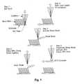
- the standard wire bonding operationis shown in FIG. 1 and starts by forming a ball on the end of a (preferably) gold wire 110 that is threaded through a hollow pointed ceramic tool called a capillary 115 .
- the ball 112is pressed against the first bonding surface 116 of substrate 118 while the substrate 118 is heated from below and ultrasonic energy is applied through the capillary 115 as shown in step 1 of FIG. 1.
- the metallurgy on the surface of the substrateis critical to the wire bonding process.
- the capillary 115is raised while the substrate is moved (shown by arrow 120 ) to create a loop shape in the wire (FIG. 1—step 2 ).
- the capillary 115is then lowered to press the side 124 of the wire against the second substrate 126 surface 128 to form the second bond or wedge bond 130 (FIG. 1—step 3 ).
- the capillaryis raised slightly indicated by arrow 132 and a mechanical clamp is actuated to hold the wire in place while the capillary is raised again to break the wire at the end of the wedge bond 134 (FIG. 1—step 4 ).
- the ballis formed on the end of the gold bond wire by placing an electrode below the tip 136 of the wire and using a high voltage electrical discharge to melt the end of the wire (FIG. 1—step 5 ).
- FIG. 2shows a cross section of an electronic circuit component ( 11 ) and several angled flying leads ( 10 ) attached to the first surface ( 12 ) of the component ( 11 ) according to the present invention.
- the angled flying leads ( 10 )can be attached to a variety of different electronic circuit components ( 11 ).
- the angled flying leads ( 10 )are bonded to metallized circuit pads ( 13 ) on the first surface ( 12 ) of the electronic circuit component ( 11 ).
- the electronic circuit component ( 11 )must provide a rigid base for the thermosonic wire bonding process to be successful.
- FIGS. 1, 2, and 3 of the angled flying lead wire bonding processare essentially the same as a standard thermosonic wire bonding process.
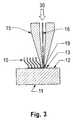
- An electrical discharge ( 22 ) from an electronic flame off (EFO) unit ( 21 )is used to melt the end of the bond wire ( 16 ) extending through the tip of a ceramic capillary tool ( 15 ).
- the electrical discharge ( 22 )is controlled to provide a consistent sized ball ( 14 ) on the end of the bond wire ( 16 ).
- FIG. 3shows the ceramic capillary tool ( 15 ) used to press the ball shaped end of the bond wire ( 16 ) against the metallized pad ( 13 ) on the surface of the electronic circuit component ( 11 ).
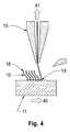
- FIG. 4shows the movement of the electronic circuit component ( 40 ) and the movement of the ceramic capillary tool ( 41 ).
- the movement of the electronic circuit component ( 40 )is used to define the offset between the free end ( 18 ) of the angled flying lead ( 10 ) and the ball bond ( 19 ) attached to the electronic circuit component ( 11 ).
- the movement of the ceramic capillary tool ( 15 )provides sufficient slack in the bond wire to minimize stress to the ball bond ( 19 ) during the subsequent operations.
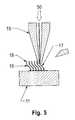
- FIG. 5shows additional movement of the ceramic capillary tool ( 50 ) that is used to form the angled and curved geometry ( 17 ) of the angled flying lead ( 10 ).
- the movement of the capillary tool ( 50 )must be controlled to prevent deformation of the adjacent angled flying leads ( 10 ).
- FIG. 6shows the shear blade ( 60 ) that is used to sever the bond wire ( 62 ) to form the free end ( 18 ) of the angled flying lead ( 10 ).
- the shear blade ( 60 )is precisely located ( 61 ) to ensure accurate positioning of the free end ( 18 ) of the angled flying lead ( 10 ).
- a clampis used to hold the bond wire while the ceramic capillary tool ( 15 ) is raised ( 62 ) and the bond wire is severed at the tip of the shear blade ( 60 ).
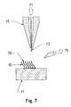
- FIG. 7shows the retraction of the shear blade ( 70 ) and the upward movement of the ceramic capillary tool ( 71 ).
- the end of the bond wire ( 72 ) extending through the tip of the ceramic capillary toolis used for the next ball bond and the process is repeated to form the desired number of angled flying leads ( 10 ) on the electronic circuit component ( 11 ).
- FIG. 8shows an alternate embodiment of the wire cutting process shown in FIG. 5.
- the alternate wire cutting process shown in FIG. 7uses two shear blades ( 80 , 83 ) instead of a single blade.
- the movement and positioning ( 81 , 84 ) of the two blades ( 80 , 83 )is synchronized to nick the wire on opposites sides and allow the wire to fracture at this point.
- the double-blade configurationcan be used for cutting wires that have a high tensile strength.
- the two blade configurationalso significantly improves wire positioning accuracy.
- FIG. 9shows a second alternate embodiment of the wire cutting process similar to the two blade process shown in FIG. 8.
- the second alternate wire cutting process shown in FIG. 9is used for creating straight wires ( 100 ) attached to an electronic circuit component ( 11 ).
- the movement and positioning ( 91 , 94 ) of the two blades ( 90 , 93 )is controlled to nick the opposite sides of the wire and allow the wire to fracture at this point.
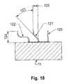
- FIG. 10shows three wire configurations ( 120 , 121 , 122 ) attached to an electronic circuit component ( 11 ) using the angled flying lead wire bonding process. All three of the wires ( 120 , 121 , 122 ) are created with the height ( 124 ) from the surface of the electronic circuit component ( 11 ).
- the three wire configurationsinclude a straight wire ( 120 ), an angled wire ( 121 ), and a wire ( 122 ) with a section parallel to the surface of the electronic circuit component ( 11 ). Variations of these three wire configurations ( 120 , 121 , 122 ) can be created including wires with different angles ( 123 ) and different wire offset ( 125 ) dimensions as shown on the angled wire ( 121 ).
- FIG. 11shows four wire configurations ( 130 , 131 , 133 , 134 ) attached to an electronic circuit component ( 11 ) using the angled flying lead wire bonding process.
- the four wire configurationsinclude two straight wires ( 130 , 131 ) with different wire heights ( 132 , 136 ) and two angled wires ( 133 , 134 ) with two different wire heights ( 135 , 137 ).
- FIGS. 12 and 13schematically show a variety of wire shapes ( 141 , 142 , 143 , 144 , 145 , 146 , 147 , 148 ) practiced by the present invention.
- the different wire shapesare created by controlling both the down-movement of the capillary tip and the off-set move of the wire bonding stage.
- the shapescontinuously curved, piece wire curved, piece wire linear and combinations thereof.
- FIG. 13schematically shows several shapes and geometries of the wire tip ends, such as straight ( 167 ), straight with pointed contact ( 166 ), straight with point contact deposited with a suitable contact metallurgy ( 165 ), straight end with sharp spikes ( 164 ) and deposited with a suitable contact metal ( 163 ), ball-shaped ( 162 ), ball-shaped deposited with a suitable contact metallurgy ( 161 ) and deposited with sharp spikes ( 160 ) at the contact ends.
- FIG. 14schematically shows a frame structure ( 150 , 153 ) which can be tailored to match the thermal expansion coefficient of silicon and other materials.
- the wire tip ends ( 152 )need to be maintained in precise position before and after engagement with electronic device pads at up to 180° C.
- the various contact geometries as shown in the figureare fabricated at the end of wires to facilitate various contact and test applications.
- FIG. 15is a schematic diagram showing the structures according to the present invention in testing apparatus.
- the testing apparatus 208has a measn 207 for disposing the probe tip ends 210 in contact with contact locations 212 on the device under test 204 which is disposed on support 206 .
- the minimum spacing between angled flying leadsis dependent on the diameter of the bond wire that is used and the size and geometry of the capillary tip used for bonding the wires. Smaller diameter wires can be bonded closer together. The capillary tip geometry can be modified using a bottleneck configuration or a side relief to allow closer bonding of the flying leads.
- the maximum height for an angled flying leadis also determined by the diameter and material properties of the bond wire and the offset distance between the ball bond and the free end of the wire. Small diameter wires (0.001 to 0.002 inch) are better suited to shorter leads and larger diameter wires (0.002 to 0.003 inch) are better suited to longer leads.
- the key material properties of the wireinclude the stiffness and the tensile strength. The wire properties can be controlled by the alloys used in the wire material and the elongation factor used for forming the wire. The structures fabricated according to the methods of the present invention.
Landscapes
- Engineering & Computer Science (AREA)
- Computer Hardware Design (AREA)
- Microelectronics & Electronic Packaging (AREA)
- Power Engineering (AREA)
- Physics & Mathematics (AREA)
- General Physics & Mathematics (AREA)
- Manufacturing & Machinery (AREA)
- Mechanical Engineering (AREA)
- Condensed Matter Physics & Semiconductors (AREA)
- Ceramic Engineering (AREA)
- Wire Bonding (AREA)
Abstract
Description
- The present invention is directed to a process for bonding wires to surfaces, for example, to form electronic device probes, or to form electrical connections on electronic circuit devices and particularly to wires that are bonded at one end with the other end free.[0001]
- Wire bonding techniques were first developed back in the 1950's for connecting germanium transistors to other electronic devices. Wire bonding techniques continue to be used for the vast majority of integrated circuit device connections. Thermal energy, mechanical force and ultrasonic vibrations are used to bond the tiny wires to the device terminals.[0002]
- The Angled Flying Lead (AFL) wire bonding process disclosed herein uses the same basic processes that are used for a standard thermosonic ball bonding operation and it was developed for fabricating a variety of area array and peripheral interconnections including high density land grid array connectors and high density IC probes.[0003]
- In conventional wire bonding, schematically shown in FIG. 1, a free end of a wire is ball bonded to a contact pad on a surface. The wire is bent over and wedge bonded to another pad. The wire joining the two pads is curved. The shape of the curve is determined by the distance between the two pads which are joined. If the wire joining the two pads are severed, two wires having different shapes are formed. If it is desired that the wires bonded to the surface be used as an electronic device probe (as described herein) or to interconnect an array of contact pads on a first surface toa nother array of contact pads on a second surface which is facing the first surface, the conventional wire bonding process is not useful to fabricate such structures. To fabricate a probe for an electronic device using wires (probe wires) bonded to a surface, one end of the wire is bonded to contact pads on a support substrate for the probe wires. The other ends of the probe wires must be positioned so as to be able to contact the contact pads on device being tested. When an electronic device probe is moved into engagement with the contact pads of the device under test, the probe wires preferably flex so that the free end (probe tip) of the wires wipe across the surface of the contact pad being probed. The wiping action permits the probe tip to make good electrical contact to a contact pad. Since a probe is used many times, the probe tips of the probe wires make many thousands (preferably greater than 1000, more preferably greater than 10,000, most preferably greater than 100,000) engagements and disengagements with contact pads on devices under test resulting in many repeated bendings. The probe tip also must be flexible enough to achieve the desired degree of wiping, withstand many engagements without deforming and be sufficiently compressible to without deformation. Applicants invention provides a method and approach which can reliable form many probe wires to a desired predetermined shape to satisfy all these requirements.[0004]
- There is a need for a technique to form wires bonded to surfaces where the wires can be formed to have any desired shape to provide certain desired properties. The wires can be bonded to electrical contact pads on a surface drawn away from the surface and cut to have a free end. The wires are bent so that the free ends are placed in a predetermined shape which provide advantageous properties, such as a desired flexibility.[0005]
- It is the object of the present invention to provide a process for bonding wires to an electronic circuit device with one end of the wire attached to the surface of the device and the other end of the wire extending away from the surface of the device.[0006]
- Another object of the present invention is to provide a process for bonding wires to an electronic circuit device with the wires formed at an angle to the surface of the device.[0007]
- A further object of the present invention is to provide a process for bonding wires to an electronic circuit device with the wires having curved features.[0008]
- These and other objects, features, and advantages of the present invention will become apparent upon further consideration of the following detailed description of the invention when read in conjunction with the drawing figures, in which:[0009]
- FIG. 1 shows the standard wire bonding process steps.[0010]
- FIGS.[0011]2-6 show the preferred embodiment of the angled flying lead wire bonding process.
- FIGS.[0012]7-8 show the alternate embodiments of the angle flying lead wire bonding process.
- FIGS.[0013]9-12 show various configurations of flying lead wire geometries.
- FIG. 13 shows a variety of shapes of the wire tip ends created to facilitate the engagement of wire tips with electronic device pads.[0014]
- FIG. 14 schematically shows a frame structure to be used to control the wire position accuracy and, in the mean time, provide matched thermal coefficient to that of silicon at elevated wafer testing temperatures.[0015]
- FIG. 15 is a schematic diagram showing the structures according to the present invention in testing apparatus.[0016]
- The standard wire bonding operation is shown in FIG. 1 and starts by forming a ball on the end of a (preferably) gold wire[0017]110 that is threaded through a hollow pointed ceramic tool called a capillary115. The ball112 is pressed against the first bonding surface116 of substrate118 while the substrate118 is heated from below and ultrasonic energy is applied through the capillary115 as shown in
step 1 of FIG. 1. The metallurgy on the surface of the substrate is critical to the wire bonding process. After ball bonding the wire to the first substrate surface116, the capillary115 is raised while the substrate is moved (shown by arrow120) to create a loop shape in the wire (FIG. 1—step2). The capillary115 is then lowered to press theside 124 of the wire against the second substrate126 surface128 to form the second bond or wedge bond130 (FIG. 1—step3). The capillary is raised slightly indicated byarrow 132 and a mechanical clamp is actuated to hold the wire in place while the capillary is raised again to break the wire at the end of the wedge bond134 (FIG. 1—step4). The ball is formed on the end of the gold bond wire by placing an electrode below thetip 136 of the wire and using a high voltage electrical discharge to melt the end of the wire (FIG. 1—step5). - FIG. 2 shows a cross section of an electronic circuit component ([0018]11) and several angled flying leads (10) attached to the first surface (12) of the component (11) according to the present invention. The angled flying leads (10) can be attached to a variety of different electronic circuit components (11). The angled flying leads (10) are bonded to metallized circuit pads (13) on the first surface (12) of the electronic circuit component (11). The electronic circuit component (11) must provide a rigid base for the thermosonic wire bonding process to be successful. FIGS. 1, 2, and3 of the angled flying lead wire bonding process are essentially the same as a standard thermosonic wire bonding process. An electrical discharge (22) from an electronic flame off (EFO) unit (21) is used to melt the end of the bond wire (16) extending through the tip of a ceramic capillary tool (15). The electrical discharge (22) is controlled to provide a consistent sized ball (14) on the end of the bond wire (16).
- FIG. 3 shows the ceramic capillary tool ([0019]15) used to press the ball shaped end of the bond wire (16) against the metallized pad (13) on the surface of the electronic circuit component (11). Ultrasonic energy (30) applied through the ceramic capillary tool (15) and thermal energy applied through the base holding the electronic circuit component (11) in used to form a ball bond (19) between the bond wire (16) and the metallized pad (13) on the surface of the electronic circuit component (11).
- FIG. 4 shows the movement of the electronic circuit component ([0020]40) and the movement of the ceramic capillary tool (41). The movement of the electronic circuit component (40) is used to define the offset between the free end (18) of the angled flying lead (10) and the ball bond (19) attached to the electronic circuit component (11). The movement of the ceramic capillary tool (15) provides sufficient slack in the bond wire to minimize stress to the ball bond (19) during the subsequent operations.
- FIG. 5 shows additional movement of the ceramic capillary tool ([0021]50) that is used to form the angled and curved geometry (17) of the angled flying lead (10). The movement of the capillary tool (50) must be controlled to prevent deformation of the adjacent angled flying leads (10).
- FIG. 6 shows the shear blade ([0022]60) that is used to sever the bond wire (62) to form the free end (18) of the angled flying lead (10). The shear blade (60) is precisely located (61) to ensure accurate positioning of the free end (18) of the angled flying lead (10). A clamp is used to hold the bond wire while the ceramic capillary tool (15) is raised (62) and the bond wire is severed at the tip of the shear blade (60).
- FIG. 7 shows the retraction of the shear blade ([0023]70) and the upward movement of the ceramic capillary tool (71). The end of the bond wire (72) extending through the tip of the ceramic capillary tool is used for the next ball bond and the process is repeated to form the desired number of angled flying leads (10) on the electronic circuit component (11).
- FIG. 8 shows an alternate embodiment of the wire cutting process shown in FIG. 5. The alternate wire cutting process shown in FIG. 7 uses two shear blades ([0024]80,83) instead of a single blade. The movement and positioning (81,84) of the two blades (80,83) is synchronized to nick the wire on opposites sides and allow the wire to fracture at this point. The double-blade configuration can be used for cutting wires that have a high tensile strength. The two blade configuration also significantly improves wire positioning accuracy.
- FIG. 9 shows a second alternate embodiment of the wire cutting process similar to the two blade process shown in FIG. 8. The second alternate wire cutting process shown in FIG. 9 is used for creating straight wires ([0025]100) attached to an electronic circuit component (11). The movement and positioning (91,94) of the two blades (90,93) is controlled to nick the opposite sides of the wire and allow the wire to fracture at this point.
- FIG. 10 shows three wire configurations ([0026]120,121,122) attached to an electronic circuit component (11) using the angled flying lead wire bonding process. All three of the wires (120,121,122) are created with the height (124) from the surface of the electronic circuit component (11). The three wire configurations include a straight wire (120), an angled wire (121), and a wire (122) with a section parallel to the surface of the electronic circuit component (11). Variations of these three wire configurations (120,121,122) can be created including wires with different angles (123) and different wire offset (125) dimensions as shown on the angled wire (121).
- FIG. 11 shows four wire configurations ([0027]130,131,133,134) attached to an electronic circuit component (11) using the angled flying lead wire bonding process. The four wire configurations include two straight wires (130,131) with different wire heights (132,136) and two angled wires (133,134) with two different wire heights (135,137).
- FIGS. 12 and 13 schematically show a variety of wire shapes ([0028]141,142,143,144,145,146,147,148) practiced by the present invention. The different wire shapes are created by controlling both the down-movement of the capillary tip and the off-set move of the wire bonding stage. The shapes continuously curved, piece wire curved, piece wire linear and combinations thereof.
- FIG. 13 schematically shows several shapes and geometries of the wire tip ends, such as straight ([0029]167), straight with pointed contact (166), straight with point contact deposited with a suitable contact metallurgy (165), straight end with sharp spikes (164) and deposited with a suitable contact metal (163), ball-shaped (162), ball-shaped deposited with a suitable contact metallurgy (161) and deposited with sharp spikes (160) at the contact ends.
- FIG. 14 schematically shows a frame structure ([0030]150,153) which can be tailored to match the thermal expansion coefficient of silicon and other materials. The wire tip ends (152) need to be maintained in precise position before and after engagement with electronic device pads at up to 180° C. The various contact geometries as shown in the figure are fabricated at the end of wires to facilitate various contact and test applications.
- FIG. 15 is a schematic diagram showing the structures according to the present invention in testing apparatus. The[0031]
testing apparatus 208 has a measn207 for disposing the probe tip ends210 in contact withcontact locations 212 on the device undertest 204 which is disposed onsupport 206. - The minimum spacing between angled flying leads is dependent on the diameter of the bond wire that is used and the size and geometry of the capillary tip used for bonding the wires. Smaller diameter wires can be bonded closer together. The capillary tip geometry can be modified using a bottleneck configuration or a side relief to allow closer bonding of the flying leads. The maximum height for an angled flying lead is also determined by the diameter and material properties of the bond wire and the offset distance between the ball bond and the free end of the wire. Small diameter wires (0.001 to 0.002 inch) are better suited to shorter leads and larger diameter wires (0.002 to 0.003 inch) are better suited to longer leads. The key material properties of the wire include the stiffness and the tensile strength. The wire properties can be controlled by the alloys used in the wire material and the elongation factor used for forming the wire. The structures fabricated according to the methods of the present invention.[0032]
- The teachings of copending U.S. application Ser. No. 09/088,394 filed Jun. 1, 1998 and U.S. Pat. No. 5,371,654 are incorporated herein by reference.[0033]
- While we have described our preferred embodiments of our invention, it will be understood that those skilled in the art, both now and in the future, may make various improvements and enhancements which fall within the scope of the claims which follow. These claims should be construed to maintain the proper protection for the invention first disclosed.[0034]
Claims (28)
Priority Applications (3)
| Application Number | Priority Date | Filing Date | Title |
|---|---|---|---|
| US10/342,167US6708403B2 (en) | 1992-10-19 | 2003-01-14 | Angled flying lead wire bonding process |
| US10/736,890US7495342B2 (en) | 1992-10-19 | 2003-12-16 | Angled flying lead wire bonding process |
| US12/357,453US20090189288A1 (en) | 1992-10-19 | 2009-01-22 | Angled flying lead wire bonding process |
Applications Claiming Priority (8)
| Application Number | Priority Date | Filing Date | Title |
|---|---|---|---|
| US07/963,346US5371654A (en) | 1992-10-19 | 1992-10-19 | Three dimensional high performance interconnection package |
| US08/055,485US5635846A (en) | 1992-10-19 | 1993-04-30 | Test probe having elongated conductor embedded in an elostomeric material which is mounted on a space transformer |
| US08/754,869US5821763A (en) | 1992-10-19 | 1996-11-22 | Test probe for high density integrated circuits, methods of fabrication thereof and methods of use thereof |
| US6087797P | 1997-10-02 | 1997-10-02 | |
| US09/088,394US6300780B1 (en) | 1992-10-19 | 1998-06-01 | High density integrated circuit apparatus, test probe and methods of use thereof |
| US09/164,470US6295729B1 (en) | 1992-10-19 | 1998-10-01 | Angled flying lead wire bonding process |
| US09/871,536US6526655B2 (en) | 1992-10-19 | 2001-05-31 | Angled flying lead wire bonding process |
| US10/342,167US6708403B2 (en) | 1992-10-19 | 2003-01-14 | Angled flying lead wire bonding process |
Related Parent Applications (1)
| Application Number | Title | Priority Date | Filing Date |
|---|---|---|---|
| US09/871,536ContinuationUS6526655B2 (en) | 1992-10-19 | 2001-05-31 | Angled flying lead wire bonding process |
Related Child Applications (1)
| Application Number | Title | Priority Date | Filing Date |
|---|---|---|---|
| US10/736,890DivisionUS7495342B2 (en) | 1992-10-19 | 2003-12-16 | Angled flying lead wire bonding process |
Publications (2)
| Publication Number | Publication Date |
|---|---|
| US20030106213A1true US20030106213A1 (en) | 2003-06-12 |
| US6708403B2 US6708403B2 (en) | 2004-03-23 |
Family
ID=46203455
Family Applications (5)
| Application Number | Title | Priority Date | Filing Date |
|---|---|---|---|
| US09/164,470Expired - LifetimeUS6295729B1 (en) | 1992-10-19 | 1998-10-01 | Angled flying lead wire bonding process |
| US09/871,536Expired - LifetimeUS6526655B2 (en) | 1992-10-19 | 2001-05-31 | Angled flying lead wire bonding process |
| US10/342,167Expired - LifetimeUS6708403B2 (en) | 1992-10-19 | 2003-01-14 | Angled flying lead wire bonding process |
| US10/736,890Expired - Fee RelatedUS7495342B2 (en) | 1992-10-19 | 2003-12-16 | Angled flying lead wire bonding process |
| US12/357,453AbandonedUS20090189288A1 (en) | 1992-10-19 | 2009-01-22 | Angled flying lead wire bonding process |
Family Applications Before (2)
| Application Number | Title | Priority Date | Filing Date |
|---|---|---|---|
| US09/164,470Expired - LifetimeUS6295729B1 (en) | 1992-10-19 | 1998-10-01 | Angled flying lead wire bonding process |
| US09/871,536Expired - LifetimeUS6526655B2 (en) | 1992-10-19 | 2001-05-31 | Angled flying lead wire bonding process |
Family Applications After (2)
| Application Number | Title | Priority Date | Filing Date |
|---|---|---|---|
| US10/736,890Expired - Fee RelatedUS7495342B2 (en) | 1992-10-19 | 2003-12-16 | Angled flying lead wire bonding process |
| US12/357,453AbandonedUS20090189288A1 (en) | 1992-10-19 | 2009-01-22 | Angled flying lead wire bonding process |
Country Status (1)
| Country | Link |
|---|---|
| US (5) | US6295729B1 (en) |
Cited By (38)
| Publication number | Priority date | Publication date | Assignee | Title |
|---|---|---|---|---|
| US8372741B1 (en)* | 2012-02-24 | 2013-02-12 | Invensas Corporation | Method for package-on-package assembly with wire bonds to encapsulation surface |
| US8482111B2 (en) | 2010-07-19 | 2013-07-09 | Tessera, Inc. | Stackable molded microelectronic packages |
| US8525314B2 (en) | 2004-11-03 | 2013-09-03 | Tessera, Inc. | Stacked packaging improvements |
| US8618659B2 (en) | 2011-05-03 | 2013-12-31 | Tessera, Inc. | Package-on-package assembly with wire bonds to encapsulation surface |
| US8623706B2 (en) | 2010-11-15 | 2014-01-07 | Tessera, Inc. | Microelectronic package with terminals on dielectric mass |
| US8728865B2 (en) | 2005-12-23 | 2014-05-20 | Tessera, Inc. | Microelectronic packages and methods therefor |
| US8836136B2 (en) | 2011-10-17 | 2014-09-16 | Invensas Corporation | Package-on-package assembly with wire bond vias |
| US8835228B2 (en) | 2012-05-22 | 2014-09-16 | Invensas Corporation | Substrate-less stackable package with wire-bond interconnect |
| US8878353B2 (en) | 2012-12-20 | 2014-11-04 | Invensas Corporation | Structure for microelectronic packaging with bond elements to encapsulation surface |
| US8883563B1 (en) | 2013-07-15 | 2014-11-11 | Invensas Corporation | Fabrication of microelectronic assemblies having stack terminals coupled by connectors extending through encapsulation |
| US8975738B2 (en) | 2012-11-12 | 2015-03-10 | Invensas Corporation | Structure for microelectronic packaging with terminals on dielectric mass |
| US9023691B2 (en) | 2013-07-15 | 2015-05-05 | Invensas Corporation | Microelectronic assemblies with stack terminals coupled by connectors extending through encapsulation |
| US9034696B2 (en) | 2013-07-15 | 2015-05-19 | Invensas Corporation | Microelectronic assemblies having reinforcing collars on connectors extending through encapsulation |
| US9082753B2 (en) | 2013-11-12 | 2015-07-14 | Invensas Corporation | Severing bond wire by kinking and twisting |
| US9087815B2 (en) | 2013-11-12 | 2015-07-21 | Invensas Corporation | Off substrate kinking of bond wire |
| CN105070666A (en)* | 2015-07-17 | 2015-11-18 | 北京中电科电子装备有限公司 | Chip, lead bonding method and device for packaging chip, and separating device for packaging chip |
| US9214454B2 (en) | 2014-03-31 | 2015-12-15 | Invensas Corporation | Batch process fabrication of package-on-package microelectronic assemblies |
| US9224717B2 (en) | 2011-05-03 | 2015-12-29 | Tessera, Inc. | Package-on-package assembly with wire bonds to encapsulation surface |
| US9324681B2 (en) | 2010-12-13 | 2016-04-26 | Tessera, Inc. | Pin attachment |
| US9349706B2 (en) | 2012-02-24 | 2016-05-24 | Invensas Corporation | Method for package-on-package assembly with wire bonds to encapsulation surface |
| US9391008B2 (en) | 2012-07-31 | 2016-07-12 | Invensas Corporation | Reconstituted wafer-level package DRAM |
| US9412714B2 (en) | 2014-05-30 | 2016-08-09 | Invensas Corporation | Wire bond support structure and microelectronic package including wire bonds therefrom |
| US9502390B2 (en) | 2012-08-03 | 2016-11-22 | Invensas Corporation | BVA interposer |
| US9530749B2 (en) | 2015-04-28 | 2016-12-27 | Invensas Corporation | Coupling of side surface contacts to a circuit platform |
| US9553076B2 (en) | 2010-07-19 | 2017-01-24 | Tessera, Inc. | Stackable molded microelectronic packages with area array unit connectors |
| US9583411B2 (en) | 2014-01-17 | 2017-02-28 | Invensas Corporation | Fine pitch BVA using reconstituted wafer with area array accessible for testing |
| US9601454B2 (en) | 2013-02-01 | 2017-03-21 | Invensas Corporation | Method of forming a component having wire bonds and a stiffening layer |
| US9646917B2 (en) | 2014-05-29 | 2017-05-09 | Invensas Corporation | Low CTE component with wire bond interconnects |
| US9659848B1 (en) | 2015-11-18 | 2017-05-23 | Invensas Corporation | Stiffened wires for offset BVA |
| US9685365B2 (en) | 2013-08-08 | 2017-06-20 | Invensas Corporation | Method of forming a wire bond having a free end |
| US9728527B2 (en) | 2013-11-22 | 2017-08-08 | Invensas Corporation | Multiple bond via arrays of different wire heights on a same substrate |
| CN107275243A (en)* | 2017-06-06 | 2017-10-20 | 潮州三环(集团)股份有限公司 | Weld chopper and preparation method thereof |
| US9831155B2 (en)* | 2016-03-11 | 2017-11-28 | Nanya Technology Corporation | Chip package having tilted through silicon via |
| US9852969B2 (en) | 2013-11-22 | 2017-12-26 | Invensas Corporation | Die stacks with one or more bond via arrays of wire bond wires and with one or more arrays of bump interconnects |
| US10008477B2 (en) | 2013-09-16 | 2018-06-26 | Invensas Corporation | Microelectronic element with bond elements to encapsulation surface |
| US10026717B2 (en) | 2013-11-22 | 2018-07-17 | Invensas Corporation | Multiple bond via arrays of different wire heights on a same substrate |
| US10332854B2 (en) | 2015-10-23 | 2019-06-25 | Invensas Corporation | Anchoring structure of fine pitch bva |
| US10460958B2 (en) | 2013-08-07 | 2019-10-29 | Invensas Corporation | Method of manufacturing embedded packaging with preformed vias |
Families Citing this family (66)
| Publication number | Priority date | Publication date | Assignee | Title |
|---|---|---|---|---|
| US6295729B1 (en)* | 1992-10-19 | 2001-10-02 | International Business Machines Corporation | Angled flying lead wire bonding process |
| US6232789B1 (en) | 1997-05-28 | 2001-05-15 | Cascade Microtech, Inc. | Probe holder for low current measurements |
| US5729150A (en) | 1995-12-01 | 1998-03-17 | Cascade Microtech, Inc. | Low-current probe card with reduced triboelectric current generating cables |
| US5914613A (en)* | 1996-08-08 | 1999-06-22 | Cascade Microtech, Inc. | Membrane probing system with local contact scrub |
| US6034533A (en) | 1997-06-10 | 2000-03-07 | Tervo; Paul A. | Low-current pogo probe card |
| JPH11224679A (en)* | 1998-02-06 | 1999-08-17 | Matsushita Electric Ind Co Ltd | Polymer electrolyte fuel cell and method of manufacturing the same |
| DE19823623A1 (en)* | 1998-05-27 | 1999-12-02 | Bosch Gmbh Robert | Method and contact point for establishing an electrical connection |
| US6256882B1 (en) | 1998-07-14 | 2001-07-10 | Cascade Microtech, Inc. | Membrane probing system |
| US6578264B1 (en) | 1999-06-04 | 2003-06-17 | Cascade Microtech, Inc. | Method for constructing a membrane probe using a depression |
| US6838890B2 (en) | 2000-02-25 | 2005-01-04 | Cascade Microtech, Inc. | Membrane probing system |
| DE20114544U1 (en) | 2000-12-04 | 2002-02-21 | Cascade Microtech, Inc., Beaverton, Oreg. | wafer probe |
| US7355420B2 (en) | 2001-08-21 | 2008-04-08 | Cascade Microtech, Inc. | Membrane probing system |
| KR100864916B1 (en) | 2002-05-23 | 2008-10-22 | 캐스케이드 마이크로테크 인코포레이티드 | Probes for Testing Devices Under Test |
| US6724205B1 (en) | 2002-11-13 | 2004-04-20 | Cascade Microtech, Inc. | Probe for combined signals |
| US7271497B2 (en)* | 2003-03-10 | 2007-09-18 | Fairchild Semiconductor Corporation | Dual metal stud bumping for flip chip applications |
| US8896397B2 (en)* | 2003-04-16 | 2014-11-25 | Intellectual Ventures Fund 77 Llc | Surface acoustic wave device and method of adjusting LC component of surface acoustic wave device |
| JP4381714B2 (en)* | 2003-04-16 | 2009-12-09 | Okiセミコンダクタ株式会社 | Surface acoustic wave device, surface acoustic wave device, and method of manufacturing surface acoustic wave device |
| US7057404B2 (en) | 2003-05-23 | 2006-06-06 | Sharp Laboratories Of America, Inc. | Shielded probe for testing a device under test |
| US20040249825A1 (en)* | 2003-06-05 | 2004-12-09 | International Business Machines Corporation | Administering devices with dynamic action lists |
| US20050051600A1 (en)* | 2003-09-10 | 2005-03-10 | Texas Instruments Incorporated | Method and system for stud bumping |
| US20050067382A1 (en)* | 2003-09-26 | 2005-03-31 | Gary Gillotti | Fine pitch electronic flame-off wand electrode |
| DE10357822A1 (en)* | 2003-12-09 | 2005-07-07 | Hesse & Knipps Gmbh | cutter |
| WO2005065258A2 (en) | 2003-12-24 | 2005-07-21 | Cascade Microtech, Inc. | Active wafer probe |
| US7407080B2 (en)* | 2004-04-02 | 2008-08-05 | Chippac, Inc. | Wire bond capillary tip |
| KR101157449B1 (en) | 2004-07-07 | 2012-06-22 | 캐스케이드 마이크로테크 인코포레이티드 | Probe head having a membrane suspended probe |
| US7172431B2 (en) | 2004-08-27 | 2007-02-06 | International Business Machines Corporation | Electrical connector design and contact geometry and method of use thereof and methods of fabrication thereof |
| EP1789812A2 (en) | 2004-09-13 | 2007-05-30 | Cascade Microtech, Inc. | Double sided probing structures |
| CN101288205B (en)* | 2004-12-16 | 2011-09-21 | 国际商业机器公司 | Metallized Elastomer Electrical Contacts |
| US7771208B2 (en) | 2004-12-16 | 2010-08-10 | International Business Machines Corporation | Metalized elastomeric electrical contacts |
| US7464854B2 (en)* | 2005-01-25 | 2008-12-16 | Kulicke And Soffa Industries, Inc. | Method and apparatus for forming a low profile wire loop |
| US7535247B2 (en) | 2005-01-31 | 2009-05-19 | Cascade Microtech, Inc. | Interface for testing semiconductors |
| US7656172B2 (en) | 2005-01-31 | 2010-02-02 | Cascade Microtech, Inc. | System for testing semiconductors |
| US7449899B2 (en) | 2005-06-08 | 2008-11-11 | Cascade Microtech, Inc. | Probe for high frequency signals |
| JP5080459B2 (en) | 2005-06-13 | 2012-11-21 | カスケード マイクロテック インコーポレイテッド | Wideband active / passive differential signal probe |
| US7609077B2 (en) | 2006-06-09 | 2009-10-27 | Cascade Microtech, Inc. | Differential signal probe with integral balun |
| US7403028B2 (en) | 2006-06-12 | 2008-07-22 | Cascade Microtech, Inc. | Test structure and probe for differential signals |
| US7764072B2 (en) | 2006-06-12 | 2010-07-27 | Cascade Microtech, Inc. | Differential signal probing system |
| US7443186B2 (en) | 2006-06-12 | 2008-10-28 | Cascade Microtech, Inc. | On-wafer test structures for differential signals |
| US7723999B2 (en) | 2006-06-12 | 2010-05-25 | Cascade Microtech, Inc. | Calibration structures for differential signal probing |
| US8832936B2 (en)* | 2007-04-30 | 2014-09-16 | International Business Machines Corporation | Method of forming metallized elastomeric electrical contacts |
| US7876114B2 (en) | 2007-08-08 | 2011-01-25 | Cascade Microtech, Inc. | Differential waveguide probe |
| JP5164490B2 (en)* | 2007-09-13 | 2013-03-21 | ルネサスエレクトロニクス株式会社 | Semiconductor device and manufacturing method thereof |
| US7888957B2 (en) | 2008-10-06 | 2011-02-15 | Cascade Microtech, Inc. | Probing apparatus with impedance optimized interface |
| JP2010123817A (en)* | 2008-11-21 | 2010-06-03 | Fujitsu Ltd | Wire bonding method, electronic apparatus, and method of manufacturing the same |
| US8410806B2 (en) | 2008-11-21 | 2013-04-02 | Cascade Microtech, Inc. | Replaceable coupon for a probing apparatus |
| US8476538B2 (en)* | 2010-03-08 | 2013-07-02 | Formfactor, Inc. | Wiring substrate with customization layers |
| US7918378B1 (en)* | 2010-08-06 | 2011-04-05 | National Semiconductor Corporation | Wire bonding deflector for a wire bonder |
| US9043179B2 (en)* | 2011-01-06 | 2015-05-26 | International Business Machines Corporation | Voltage-driven intelligent characterization bench for semiconductor |
| US9021682B2 (en)* | 2011-12-29 | 2015-05-05 | Taiwan Semiconductor Manufacturing Company, Ltd. | Apparatus for stud bump formation |
| US8946757B2 (en) | 2012-02-17 | 2015-02-03 | Invensas Corporation | Heat spreading substrate with embedded interconnects |
| US9502371B2 (en)* | 2012-07-17 | 2016-11-22 | Kulicke And Soffa Industries, Inc. | Methods of forming wire interconnect structures |
| US8540136B1 (en)* | 2012-09-06 | 2013-09-24 | Taiwan Semiconductor Manufacturing Company, Ltd. | Methods for stud bump formation and apparatus for performing the same |
| DE102013211405B4 (en)* | 2013-06-18 | 2020-06-04 | Infineon Technologies Ag | METHOD FOR PRODUCING A SEMICONDUCTOR MODULE |
| GB2521619A (en)* | 2013-12-23 | 2015-07-01 | Nokia Technologies Oy | An apparatus and associated methods for flexible carrier substrates |
| US10381326B2 (en) | 2014-05-28 | 2019-08-13 | Invensas Corporation | Structure and method for integrated circuits packaging with increased density |
| US9735084B2 (en) | 2014-12-11 | 2017-08-15 | Invensas Corporation | Bond via array for thermal conductivity |
| US9888579B2 (en) | 2015-03-05 | 2018-02-06 | Invensas Corporation | Pressing of wire bond wire tips to provide bent-over tips |
| US9502372B1 (en) | 2015-04-30 | 2016-11-22 | Invensas Corporation | Wafer-level packaging using wire bond wires in place of a redistribution layer |
| US9761554B2 (en) | 2015-05-07 | 2017-09-12 | Invensas Corporation | Ball bonding metal wire bond wires to metal pads |
| US9490222B1 (en) | 2015-10-12 | 2016-11-08 | Invensas Corporation | Wire bond wires for interference shielding |
| US10490528B2 (en) | 2015-10-12 | 2019-11-26 | Invensas Corporation | Embedded wire bond wires |
| US10181457B2 (en) | 2015-10-26 | 2019-01-15 | Invensas Corporation | Microelectronic package for wafer-level chip scale packaging with fan-out |
| US10043779B2 (en) | 2015-11-17 | 2018-08-07 | Invensas Corporation | Packaged microelectronic device for a package-on-package device |
| US9984992B2 (en) | 2015-12-30 | 2018-05-29 | Invensas Corporation | Embedded wire bond wires for vertical integration with separate surface mount and wire bond mounting surfaces |
| US9935075B2 (en) | 2016-07-29 | 2018-04-03 | Invensas Corporation | Wire bonding method and apparatus for electromagnetic interference shielding |
| US10299368B2 (en) | 2016-12-21 | 2019-05-21 | Invensas Corporation | Surface integrated waveguides and circuit structures therefor |
Family Cites Families (18)
| Publication number | Priority date | Publication date | Assignee | Title |
|---|---|---|---|---|
| US3357090A (en)* | 1963-05-23 | 1967-12-12 | Transitron Electronic Corp | Vibratory welding tip and method of welding |
| US3605813A (en) | 1968-04-10 | 1971-09-20 | Nippon Denso Co | Control valve means of the negative pressure differential type |
| US3648354A (en)* | 1969-11-17 | 1972-03-14 | Gen Motors Corp | Tailless bonder for filamentary wire leads |
| GB1460146A (en) | 1973-02-13 | 1976-12-31 | Girling Ltd | Control valve assemblies for air braking systems |
| DE2403770A1 (en) | 1974-01-26 | 1975-08-14 | Bosch Gmbh Robert | ELECTROMAGNETIC 3-WAY VALVE ARRANGEMENT |
| US5476211A (en)* | 1993-11-16 | 1995-12-19 | Form Factor, Inc. | Method of manufacturing electrical contacts, using a sacrificial member |
| US5917707A (en)* | 1993-11-16 | 1999-06-29 | Formfactor, Inc. | Flexible contact structure with an electrically conductive shell |
| JPS62176138A (en)* | 1986-01-29 | 1987-08-01 | Toshiba Corp | Wire bonding device |
| US5285949A (en)* | 1987-01-26 | 1994-02-15 | Hitachi, Ltd. | Wire-bonding method, wire-bonding apparatus, and semiconductor device produced by the wire-bonding method |
| US5152450A (en)* | 1987-01-26 | 1992-10-06 | Hitachi, Ltd. | Wire-bonding method, wire-bonding apparatus,and semiconductor device produced by the wire-bonding method |
| EP0276928B1 (en)* | 1987-01-26 | 1994-10-26 | Hitachi, Ltd. | Wire Bonding |
| US5098305A (en)* | 1987-05-21 | 1992-03-24 | Cray Research, Inc. | Memory metal electrical connector |
| US5031821A (en)* | 1988-08-19 | 1991-07-16 | Hitachi, Ltd. | Semiconductor integrated circuit device, method for producing or assembling same, and producing or assembling apparatus for use in the method |
| US5223741A (en)* | 1989-09-01 | 1993-06-29 | Tactical Fabs, Inc. | Package for an integrated circuit structure |
| US5422435A (en)* | 1992-05-22 | 1995-06-06 | National Semiconductor Corporation | Stacked multi-chip modules and method of manufacturing |
| US6295729B1 (en)* | 1992-10-19 | 2001-10-02 | International Business Machines Corporation | Angled flying lead wire bonding process |
| US5371654A (en)* | 1992-10-19 | 1994-12-06 | International Business Machines Corporation | Three dimensional high performance interconnection package |
| US5495667A (en)* | 1994-11-07 | 1996-03-05 | Micron Technology, Inc. | Method for forming contact pins for semiconductor dice and interconnects |
- 1998
- 1998-10-01USUS09/164,470patent/US6295729B1/ennot_activeExpired - Lifetime
- 2001
- 2001-05-31USUS09/871,536patent/US6526655B2/ennot_activeExpired - Lifetime
- 2003
- 2003-01-14USUS10/342,167patent/US6708403B2/ennot_activeExpired - Lifetime
- 2003-12-16USUS10/736,890patent/US7495342B2/ennot_activeExpired - Fee Related
- 2009
- 2009-01-22USUS12/357,453patent/US20090189288A1/ennot_activeAbandoned
Cited By (78)
| Publication number | Priority date | Publication date | Assignee | Title |
|---|---|---|---|---|
| US9570416B2 (en) | 2004-11-03 | 2017-02-14 | Tessera, Inc. | Stacked packaging improvements |
| US9153562B2 (en) | 2004-11-03 | 2015-10-06 | Tessera, Inc. | Stacked packaging improvements |
| US8525314B2 (en) | 2004-11-03 | 2013-09-03 | Tessera, Inc. | Stacked packaging improvements |
| US8531020B2 (en) | 2004-11-03 | 2013-09-10 | Tessera, Inc. | Stacked packaging improvements |
| US8927337B2 (en) | 2004-11-03 | 2015-01-06 | Tessera, Inc. | Stacked packaging improvements |
| US8728865B2 (en) | 2005-12-23 | 2014-05-20 | Tessera, Inc. | Microelectronic packages and methods therefor |
| US9984901B2 (en) | 2005-12-23 | 2018-05-29 | Tessera, Inc. | Method for making a microelectronic assembly having conductive elements |
| US9218988B2 (en) | 2005-12-23 | 2015-12-22 | Tessera, Inc. | Microelectronic packages and methods therefor |
| US10128216B2 (en) | 2010-07-19 | 2018-11-13 | Tessera, Inc. | Stackable molded microelectronic packages |
| US9570382B2 (en) | 2010-07-19 | 2017-02-14 | Tessera, Inc. | Stackable molded microelectronic packages |
| US9553076B2 (en) | 2010-07-19 | 2017-01-24 | Tessera, Inc. | Stackable molded microelectronic packages with area array unit connectors |
| US8907466B2 (en) | 2010-07-19 | 2014-12-09 | Tessera, Inc. | Stackable molded microelectronic packages |
| US9123664B2 (en) | 2010-07-19 | 2015-09-01 | Tessera, Inc. | Stackable molded microelectronic packages |
| US8482111B2 (en) | 2010-07-19 | 2013-07-09 | Tessera, Inc. | Stackable molded microelectronic packages |
| US8637991B2 (en) | 2010-11-15 | 2014-01-28 | Tessera, Inc. | Microelectronic package with terminals on dielectric mass |
| US8623706B2 (en) | 2010-11-15 | 2014-01-07 | Tessera, Inc. | Microelectronic package with terminals on dielectric mass |
| US8957527B2 (en) | 2010-11-15 | 2015-02-17 | Tessera, Inc. | Microelectronic package with terminals on dielectric mass |
| US8659164B2 (en) | 2010-11-15 | 2014-02-25 | Tessera, Inc. | Microelectronic package with terminals on dielectric mass |
| US9324681B2 (en) | 2010-12-13 | 2016-04-26 | Tessera, Inc. | Pin attachment |
| US11424211B2 (en) | 2011-05-03 | 2022-08-23 | Tessera Llc | Package-on-package assembly with wire bonds to encapsulation surface |
| US9093435B2 (en) | 2011-05-03 | 2015-07-28 | Tessera, Inc. | Package-on-package assembly with wire bonds to encapsulation surface |
| US9224717B2 (en) | 2011-05-03 | 2015-12-29 | Tessera, Inc. | Package-on-package assembly with wire bonds to encapsulation surface |
| US9691731B2 (en) | 2011-05-03 | 2017-06-27 | Tessera, Inc. | Package-on-package assembly with wire bonds to encapsulation surface |
| US8618659B2 (en) | 2011-05-03 | 2013-12-31 | Tessera, Inc. | Package-on-package assembly with wire bonds to encapsulation surface |
| US9041227B2 (en) | 2011-10-17 | 2015-05-26 | Invensas Corporation | Package-on-package assembly with wire bond vias |
| US9252122B2 (en) | 2011-10-17 | 2016-02-02 | Invensas Corporation | Package-on-package assembly with wire bond vias |
| US9761558B2 (en) | 2011-10-17 | 2017-09-12 | Invensas Corporation | Package-on-package assembly with wire bond vias |
| US10756049B2 (en) | 2011-10-17 | 2020-08-25 | Invensas Corporation | Package-on-package assembly with wire bond vias |
| US11735563B2 (en) | 2011-10-17 | 2023-08-22 | Invensas Llc | Package-on-package assembly with wire bond vias |
| US11189595B2 (en) | 2011-10-17 | 2021-11-30 | Invensas Corporation | Package-on-package assembly with wire bond vias |
| US8836136B2 (en) | 2011-10-17 | 2014-09-16 | Invensas Corporation | Package-on-package assembly with wire bond vias |
| US9105483B2 (en) | 2011-10-17 | 2015-08-11 | Invensas Corporation | Package-on-package assembly with wire bond vias |
| US9691679B2 (en) | 2012-02-24 | 2017-06-27 | Invensas Corporation | Method for package-on-package assembly with wire bonds to encapsulation surface |
| US8372741B1 (en)* | 2012-02-24 | 2013-02-12 | Invensas Corporation | Method for package-on-package assembly with wire bonds to encapsulation surface |
| US9349706B2 (en) | 2012-02-24 | 2016-05-24 | Invensas Corporation | Method for package-on-package assembly with wire bonds to encapsulation surface |
| US8772152B2 (en) | 2012-02-24 | 2014-07-08 | Invensas Corporation | Method for package-on-package assembly with wire bonds to encapsulation surface |
| US9953914B2 (en) | 2012-05-22 | 2018-04-24 | Invensas Corporation | Substrate-less stackable package with wire-bond interconnect |
| US8835228B2 (en) | 2012-05-22 | 2014-09-16 | Invensas Corporation | Substrate-less stackable package with wire-bond interconnect |
| US9917073B2 (en) | 2012-07-31 | 2018-03-13 | Invensas Corporation | Reconstituted wafer-level package dram with conductive interconnects formed in encapsulant at periphery of the package |
| US9391008B2 (en) | 2012-07-31 | 2016-07-12 | Invensas Corporation | Reconstituted wafer-level package DRAM |
| US9502390B2 (en) | 2012-08-03 | 2016-11-22 | Invensas Corporation | BVA interposer |
| US10297582B2 (en) | 2012-08-03 | 2019-05-21 | Invensas Corporation | BVA interposer |
| US8975738B2 (en) | 2012-11-12 | 2015-03-10 | Invensas Corporation | Structure for microelectronic packaging with terminals on dielectric mass |
| US8878353B2 (en) | 2012-12-20 | 2014-11-04 | Invensas Corporation | Structure for microelectronic packaging with bond elements to encapsulation surface |
| US9615456B2 (en) | 2012-12-20 | 2017-04-04 | Invensas Corporation | Microelectronic assembly for microelectronic packaging with bond elements to encapsulation surface |
| US9095074B2 (en) | 2012-12-20 | 2015-07-28 | Invensas Corporation | Structure for microelectronic packaging with bond elements to encapsulation surface |
| US9601454B2 (en) | 2013-02-01 | 2017-03-21 | Invensas Corporation | Method of forming a component having wire bonds and a stiffening layer |
| US9023691B2 (en) | 2013-07-15 | 2015-05-05 | Invensas Corporation | Microelectronic assemblies with stack terminals coupled by connectors extending through encapsulation |
| US8883563B1 (en) | 2013-07-15 | 2014-11-11 | Invensas Corporation | Fabrication of microelectronic assemblies having stack terminals coupled by connectors extending through encapsulation |
| US9034696B2 (en) | 2013-07-15 | 2015-05-19 | Invensas Corporation | Microelectronic assemblies having reinforcing collars on connectors extending through encapsulation |
| US9633979B2 (en) | 2013-07-15 | 2017-04-25 | Invensas Corporation | Microelectronic assemblies having stack terminals coupled by connectors extending through encapsulation |
| US10460958B2 (en) | 2013-08-07 | 2019-10-29 | Invensas Corporation | Method of manufacturing embedded packaging with preformed vias |
| US9685365B2 (en) | 2013-08-08 | 2017-06-20 | Invensas Corporation | Method of forming a wire bond having a free end |
| US10008477B2 (en) | 2013-09-16 | 2018-06-26 | Invensas Corporation | Microelectronic element with bond elements to encapsulation surface |
| US9087815B2 (en) | 2013-11-12 | 2015-07-21 | Invensas Corporation | Off substrate kinking of bond wire |
| US9082753B2 (en) | 2013-11-12 | 2015-07-14 | Invensas Corporation | Severing bond wire by kinking and twisting |
| US9893033B2 (en) | 2013-11-12 | 2018-02-13 | Invensas Corporation | Off substrate kinking of bond wire |
| US10026717B2 (en) | 2013-11-22 | 2018-07-17 | Invensas Corporation | Multiple bond via arrays of different wire heights on a same substrate |
| US9728527B2 (en) | 2013-11-22 | 2017-08-08 | Invensas Corporation | Multiple bond via arrays of different wire heights on a same substrate |
| US9852969B2 (en) | 2013-11-22 | 2017-12-26 | Invensas Corporation | Die stacks with one or more bond via arrays of wire bond wires and with one or more arrays of bump interconnects |
| US9837330B2 (en) | 2014-01-17 | 2017-12-05 | Invensas Corporation | Fine pitch BVA using reconstituted wafer with area array accessible for testing |
| US10529636B2 (en) | 2014-01-17 | 2020-01-07 | Invensas Corporation | Fine pitch BVA using reconstituted wafer with area array accessible for testing |
| US11990382B2 (en) | 2014-01-17 | 2024-05-21 | Adeia Semiconductor Technologies Llc | Fine pitch BVA using reconstituted wafer with area array accessible for testing |
| US11404338B2 (en) | 2014-01-17 | 2022-08-02 | Invensas Corporation | Fine pitch bva using reconstituted wafer with area array accessible for testing |
| US9583411B2 (en) | 2014-01-17 | 2017-02-28 | Invensas Corporation | Fine pitch BVA using reconstituted wafer with area array accessible for testing |
| US9812433B2 (en) | 2014-03-31 | 2017-11-07 | Invensas Corporation | Batch process fabrication of package-on-package microelectronic assemblies |
| US9214454B2 (en) | 2014-03-31 | 2015-12-15 | Invensas Corporation | Batch process fabrication of package-on-package microelectronic assemblies |
| US9356006B2 (en) | 2014-03-31 | 2016-05-31 | Invensas Corporation | Batch process fabrication of package-on-package microelectronic assemblies |
| US10032647B2 (en) | 2014-05-29 | 2018-07-24 | Invensas Corporation | Low CTE component with wire bond interconnects |
| US10475726B2 (en) | 2014-05-29 | 2019-11-12 | Invensas Corporation | Low CTE component with wire bond interconnects |
| US9646917B2 (en) | 2014-05-29 | 2017-05-09 | Invensas Corporation | Low CTE component with wire bond interconnects |
| US9412714B2 (en) | 2014-05-30 | 2016-08-09 | Invensas Corporation | Wire bond support structure and microelectronic package including wire bonds therefrom |
| US9530749B2 (en) | 2015-04-28 | 2016-12-27 | Invensas Corporation | Coupling of side surface contacts to a circuit platform |
| CN105070666A (en)* | 2015-07-17 | 2015-11-18 | 北京中电科电子装备有限公司 | Chip, lead bonding method and device for packaging chip, and separating device for packaging chip |
| US10332854B2 (en) | 2015-10-23 | 2019-06-25 | Invensas Corporation | Anchoring structure of fine pitch bva |
| US9659848B1 (en) | 2015-11-18 | 2017-05-23 | Invensas Corporation | Stiffened wires for offset BVA |
| US9831155B2 (en)* | 2016-03-11 | 2017-11-28 | Nanya Technology Corporation | Chip package having tilted through silicon via |
| CN107275243A (en)* | 2017-06-06 | 2017-10-20 | 潮州三环(集团)股份有限公司 | Weld chopper and preparation method thereof |
Also Published As
| Publication number | Publication date |
|---|---|
| US7495342B2 (en) | 2009-02-24 |
| US6708403B2 (en) | 2004-03-23 |
| US20040148773A1 (en) | 2004-08-05 |
| US6526655B2 (en) | 2003-03-04 |
| US20090189288A1 (en) | 2009-07-30 |
| US20010045012A1 (en) | 2001-11-29 |
| US6295729B1 (en) | 2001-10-02 |
Similar Documents
| Publication | Publication Date | Title |
|---|---|---|
| US6708403B2 (en) | Angled flying lead wire bonding process | |
| JP3262531B2 (en) | Bent flying lead wire bonding process | |
| US6332270B2 (en) | Method of making high density integral test probe | |
| US7276919B1 (en) | High density integral test probe | |
| EP1482314B1 (en) | Microelectronic spring contact element | |
| US5838160A (en) | Integral rigid chip test probe | |
| US6442831B1 (en) | Method for shaping spring elements | |
| US6722032B2 (en) | Method of forming a structure for electronic devices contact locations | |
| US6062879A (en) | High density test probe with rigid surface structure | |
| US5811982A (en) | High density cantilevered probe for electronic devices | |
| US6104201A (en) | Method and apparatus for passive characterization of semiconductor substrates subjected to high energy (MEV) ion implementation using high-injection surface photovoltage | |
| US5914614A (en) | High density cantilevered probe for electronic devices | |
| US9030222B2 (en) | Sharpened, oriented contact tip structures | |
| US6836962B2 (en) | Method and apparatus for shaping spring elements | |
| US7172431B2 (en) | Electrical connector design and contact geometry and method of use thereof and methods of fabrication thereof | |
| US20080030215A1 (en) | High density cantilevered probe for electronic devices | |
| EP1782077A1 (en) | Stacked tip cantilever electrical connector | |
| JP2003294787A (en) | Contactor, manufacturing method thereof and test method using contactor | |
| US6523733B2 (en) | Controlled attenuation capillary | |
| US6321969B1 (en) | Efficient energy transfer capillary | |
| US6525551B1 (en) | Probe structures for testing electrical interconnections to integrated circuit electronic devices | |
| WO1996037333A1 (en) | Ribbon-like core interconnection elements | |
| WO1996037334A1 (en) | Method and apparatus for shaping spring elements | |
| JP2000223526A (en) | Combined system, method and apparatus for wire-bonding and testing |
Legal Events
| Date | Code | Title | Description |
|---|---|---|---|
| FEPP | Fee payment procedure | Free format text:PAYOR NUMBER ASSIGNED (ORIGINAL EVENT CODE: ASPN); ENTITY STATUS OF PATENT OWNER: LARGE ENTITY | |
| STCF | Information on status: patent grant | Free format text:PATENTED CASE | |
| AS | Assignment | Owner name:TOUCHDOWN TECHNOLOGIES, INC., CALIFORNIA Free format text:ASSIGNMENT OF ASSIGNORS INTEREST;ASSIGNOR:INTERNATIONAL BUSINESS MACHINES CORPORATION;REEL/FRAME:018720/0121 Effective date:20061229 | |
| CC | Certificate of correction | ||
| FPAY | Fee payment | Year of fee payment:4 | |
| FEPP | Fee payment procedure | Free format text:PAYER NUMBER DE-ASSIGNED (ORIGINAL EVENT CODE: RMPN); ENTITY STATUS OF PATENT OWNER: LARGE ENTITY Free format text:PAYOR NUMBER ASSIGNED (ORIGINAL EVENT CODE: ASPN); ENTITY STATUS OF PATENT OWNER: LARGE ENTITY | |
| AS | Assignment | Owner name:MERITECH CAPITAL PARTNERS III L.P., CALIFORNIA Free format text:SECURITY AGREEMENT;ASSIGNOR:TOUCHDOWN TECHNOLOGIES, INC.;REEL/FRAME:022619/0478 Effective date:20090420 Owner name:MERITECH CAPITAL AFFILIATES III L.P., CALIFORNIA Free format text:SECURITY AGREEMENT;ASSIGNOR:TOUCHDOWN TECHNOLOGIES, INC.;REEL/FRAME:022619/0478 Effective date:20090420 Owner name:FIRSTMARK III, L.P., NEW YORK Free format text:SECURITY AGREEMENT;ASSIGNOR:TOUCHDOWN TECHNOLOGIES, INC.;REEL/FRAME:022619/0478 Effective date:20090420 Owner name:FIRSTMARK III OFFSHORE PARTNERS, L.P., NEW YORK Free format text:SECURITY AGREEMENT;ASSIGNOR:TOUCHDOWN TECHNOLOGIES, INC.;REEL/FRAME:022619/0478 Effective date:20090420 Owner name:ADAMS CAPITAL MANAGEMENT II, L.P., PENNSYLVANIA Free format text:SECURITY AGREEMENT;ASSIGNOR:TOUCHDOWN TECHNOLOGIES, INC.;REEL/FRAME:022619/0478 Effective date:20090420 Owner name:ADAMS CAPITAL MANAGEMENT III, L.P., PENNSYLVANIA Free format text:SECURITY AGREEMENT;ASSIGNOR:TOUCHDOWN TECHNOLOGIES, INC.;REEL/FRAME:022619/0478 Effective date:20090420 Owner name:CHANCELLOR V, L.P., CALIFORNIA Free format text:SECURITY AGREEMENT;ASSIGNOR:TOUCHDOWN TECHNOLOGIES, INC.;REEL/FRAME:022619/0478 Effective date:20090420 Owner name:CHANCELLOR V-A, L.P., CALIFORNIA Free format text:SECURITY AGREEMENT;ASSIGNOR:TOUCHDOWN TECHNOLOGIES, INC.;REEL/FRAME:022619/0478 Effective date:20090420 Owner name:CITIVENTURE 2000, L.P., CALIFORNIA Free format text:SECURITY AGREEMENT;ASSIGNOR:TOUCHDOWN TECHNOLOGIES, INC.;REEL/FRAME:022619/0478 Effective date:20090420 Owner name:E-INVEST LIMITED, SINGAPORE Free format text:SECURITY AGREEMENT;ASSIGNOR:TOUCHDOWN TECHNOLOGIES, INC.;REEL/FRAME:022619/0478 Effective date:20090420 Owner name:FALCON FUND, CALIFORNIA Free format text:SECURITY AGREEMENT;ASSIGNOR:TOUCHDOWN TECHNOLOGIES, INC.;REEL/FRAME:022619/0478 Effective date:20090420 Owner name:THE ROBERT AND ANNE POCHOWSKI LIVING TRUST DATED M Free format text:SECURITY AGREEMENT;ASSIGNOR:TOUCHDOWN TECHNOLOGIES, INC.;REEL/FRAME:022619/0478 Effective date:20090420 Owner name:FORT WASHINGTON PRIVATE EQUITY INVESTORS IV, L.P., Free format text:SECURITY AGREEMENT;ASSIGNOR:TOUCHDOWN TECHNOLOGIES, INC.;REEL/FRAME:022619/0478 Effective date:20090420 Owner name:KENTUCKY CO-INVESTMENT PARTNERS, L.P., OHIO Free format text:SECURITY AGREEMENT;ASSIGNOR:TOUCHDOWN TECHNOLOGIES, INC.;REEL/FRAME:022619/0478 Effective date:20090420 Owner name:J.F. SHEA CO., AS NOMINEE 2000-129, CALIFORNIA Free format text:SECURITY AGREEMENT;ASSIGNOR:TOUCHDOWN TECHNOLOGIES, INC.;REEL/FRAME:022619/0478 Effective date:20090420 Owner name:3VS1 ASIA GROWTH FUND LTD., SINGAPORE Free format text:SECURITY AGREEMENT;ASSIGNOR:TOUCHDOWN TECHNOLOGIES, INC.;REEL/FRAME:022619/0478 Effective date:20090420 Owner name:MERITECH CAPITAL PARTNERS III L.P.,CALIFORNIA Free format text:SECURITY AGREEMENT;ASSIGNOR:TOUCHDOWN TECHNOLOGIES, INC.;REEL/FRAME:022619/0478 Effective date:20090420 Owner name:MERITECH CAPITAL AFFILIATES III L.P.,CALIFORNIA Free format text:SECURITY AGREEMENT;ASSIGNOR:TOUCHDOWN TECHNOLOGIES, INC.;REEL/FRAME:022619/0478 Effective date:20090420 Owner name:FIRSTMARK III, L.P.,NEW YORK Free format text:SECURITY AGREEMENT;ASSIGNOR:TOUCHDOWN TECHNOLOGIES, INC.;REEL/FRAME:022619/0478 Effective date:20090420 Owner name:FIRSTMARK III OFFSHORE PARTNERS, L.P.,NEW YORK Free format text:SECURITY AGREEMENT;ASSIGNOR:TOUCHDOWN TECHNOLOGIES, INC.;REEL/FRAME:022619/0478 Effective date:20090420 Owner name:ADAMS CAPITAL MANAGEMENT II, L.P.,PENNSYLVANIA Free format text:SECURITY AGREEMENT;ASSIGNOR:TOUCHDOWN TECHNOLOGIES, INC.;REEL/FRAME:022619/0478 Effective date:20090420 Owner name:ADAMS CAPITAL MANAGEMENT III, L.P.,PENNSYLVANIA Free format text:SECURITY AGREEMENT;ASSIGNOR:TOUCHDOWN TECHNOLOGIES, INC.;REEL/FRAME:022619/0478 Effective date:20090420 Owner name:CHANCELLOR V, L.P.,CALIFORNIA Free format text:SECURITY AGREEMENT;ASSIGNOR:TOUCHDOWN TECHNOLOGIES, INC.;REEL/FRAME:022619/0478 Effective date:20090420 Owner name:CHANCELLOR V-A, L.P.,CALIFORNIA Free format text:SECURITY AGREEMENT;ASSIGNOR:TOUCHDOWN TECHNOLOGIES, INC.;REEL/FRAME:022619/0478 Effective date:20090420 Owner name:CITIVENTURE 2000, L.P.,CALIFORNIA Free format text:SECURITY AGREEMENT;ASSIGNOR:TOUCHDOWN TECHNOLOGIES, INC.;REEL/FRAME:022619/0478 Effective date:20090420 Owner name:E-INVEST LIMITED,SINGAPORE Free format text:SECURITY AGREEMENT;ASSIGNOR:TOUCHDOWN TECHNOLOGIES, INC.;REEL/FRAME:022619/0478 Effective date:20090420 Owner name:FALCON FUND,CALIFORNIA Free format text:SECURITY AGREEMENT;ASSIGNOR:TOUCHDOWN TECHNOLOGIES, INC.;REEL/FRAME:022619/0478 Effective date:20090420 Owner name:KENTUCKY CO-INVESTMENT PARTNERS, L.P.,OHIO Free format text:SECURITY AGREEMENT;ASSIGNOR:TOUCHDOWN TECHNOLOGIES, INC.;REEL/FRAME:022619/0478 Effective date:20090420 Owner name:J.F. SHEA CO., AS NOMINEE 2000-129,CALIFORNIA Free format text:SECURITY AGREEMENT;ASSIGNOR:TOUCHDOWN TECHNOLOGIES, INC.;REEL/FRAME:022619/0478 Effective date:20090420 Owner name:3VS1 ASIA GROWTH FUND LTD.,SINGAPORE Free format text:SECURITY AGREEMENT;ASSIGNOR:TOUCHDOWN TECHNOLOGIES, INC.;REEL/FRAME:022619/0478 Effective date:20090420 | |
| AS | Assignment | Owner name:TOUCHDOWN TECHNOLOGIES, INC., CALIFORNIA Free format text:RELEASE BY SECURED PARTY;ASSIGNORS:MERITECH CAPITAL PARTNERS III L.P.;MERITECH CAPITAL AFFILIATES III L.P.;FIRSTMARK III, L.P.;AND OTHERS;REEL/FRAME:022824/0902 Effective date:20090615 Owner name:TOUCHDOWN TECHNOLOGIES, INC.,CALIFORNIA Free format text:RELEASE BY SECURED PARTY;ASSIGNORS:MERITECH CAPITAL PARTNERS III L.P.;MERITECH CAPITAL AFFILIATES III L.P.;FIRSTMARK III, L.P.;AND OTHERS;REEL/FRAME:022824/0902 Effective date:20090615 | |
| AS | Assignment | Owner name:LAKE ACQUISITION, INC., CALIFORNIA Free format text:ASSIGNMENT OF ASSIGNORS INTEREST;ASSIGNOR:TOUCHDOWN TECHNOLOGIES, INC.;REEL/FRAME:022868/0913 Effective date:20090615 Owner name:LAKE ACQUISITION, INC.,CALIFORNIA Free format text:ASSIGNMENT OF ASSIGNORS INTEREST;ASSIGNOR:TOUCHDOWN TECHNOLOGIES, INC.;REEL/FRAME:022868/0913 Effective date:20090615 | |
| AS | Assignment | Owner name:TOUCHDOWN TECHNOLOGIES, INC., CALIFORNIA Free format text:CHANGE OF NAME;ASSIGNOR:LAKE ACQUISITION, INC.;REEL/FRAME:023003/0771 Effective date:20090624 Owner name:TOUCHDOWN TECHNOLOGIES, INC.,CALIFORNIA Free format text:CHANGE OF NAME;ASSIGNOR:LAKE ACQUISITION, INC.;REEL/FRAME:023003/0771 Effective date:20090624 | |
| FPAY | Fee payment | Year of fee payment:8 | |
| AS | Assignment | Owner name:VERIGY US, INC., CALIFORNIA Free format text:ASSIGNMENT OF ASSIGNORS INTEREST;ASSIGNOR:TOUCHDOWN TECHNOLOGIES, INC.;REEL/FRAME:027906/0497 Effective date:20120321 | |
| AS | Assignment | Owner name:ADVANTEST AMERICA, INC, CALIFORNIA Free format text:CHANGE OF NAME;ASSIGNOR:VERIGY US, INC;REEL/FRAME:028054/0852 Effective date:20120331 | |
| FPAY | Fee payment | Year of fee payment:12 | |
| AS | Assignment | Owner name:FORMFACTOR, INC., CALIFORNIA Free format text:ASSIGNMENT OF ASSIGNORS INTEREST;ASSIGNOR:ADVANTEST AMERICA, INC.;REEL/FRAME:057219/0246 Effective date:20201126 | |
| AS | Assignment | Owner name:WELLS FARGO BANK, NATIONAL ASSOCIATION, AS ADMINISTRATIVE AGENT, TEXAS Free format text:SECURITY INTEREST;ASSIGNOR:FORMFACTOR, INC.;REEL/FRAME:072263/0272 Effective date:20250729 |